chapter 2 the physics of solids
TRANSCRIPT

8/14/2019 Chapter 2 THE PHYSICS OF SOLIDS
http://slidepdf.com/reader/full/chapter-2-the-physics-of-solids 1/122
Electronic Materials and
Processing IChapter 2
THE PHYSICS OF SOLIDS

8/14/2019 Chapter 2 THE PHYSICS OF SOLIDS
http://slidepdf.com/reader/full/chapter-2-the-physics-of-solids 2/122
Chapter 2
THE PHYSICS OF SOLIDS2.1 ELECTRONIC BAND STRUCTURES OF SOLIDS
-Two approaches considering how the weakly bound
(valence) electrons interact with the positively charged
atomic cores and with other valence electrons in a solid.
First the direct approach of solutions of the
Schrödinger equation, which governs the motion of
electrons in an arbitrary potentialThe second approach is to follow the electronic
orbitals of the atoms as they mix themselves into
molecular states and then join to form bonding and
antibonding combinations and finally bands of states

8/14/2019 Chapter 2 THE PHYSICS OF SOLIDS
http://slidepdf.com/reader/full/chapter-2-the-physics-of-solids 3/122
-Specific states of electrons described by quantum numbers:
principle number n, angular momentum number l, magnetic
quantum number ml and spin moment number ms .-Each set of quantum numbers results in a set of “wave
functions” ψn,j,m which describe the probability of finding an
electron around a given location at a given time.
- s state: spherical shape; p state: dumbbel shape
-Quantum mechanics:Electrons behave as both
waves and particles
-The particle must be
described by a probability
distribution (its wave
function) rather than by
indicating a specific
position

8/14/2019 Chapter 2 THE PHYSICS OF SOLIDS
http://slidepdf.com/reader/full/chapter-2-the-physics-of-solids 4/122
-The total energy, Etot, of an electron is the sum of its
potential and kinetic energies.
-In classical terms :
Etot = p2 /2m + U(r) 2.1
where U(r) describes the local potential energy of theparticle at position r and Ekin (Ekin= p2 /2m) is the kinetic
energy in which m is the particle mass and p is the
momentum.
- Object is small enough, quantum mechanical behavior
becom dominant, 2.1 should be described in quantum
mechanics
-Uncertainty principle: the exact energy (E) can not be
described at any specific time (t) within an accuracy better
than :
where is Plank’s constant divided by 2π.
E t ∆ ∆ =

8/14/2019 Chapter 2 THE PHYSICS OF SOLIDS
http://slidepdf.com/reader/full/chapter-2-the-physics-of-solids 5/122
-Electron total energy is given by the change in the wave
function, Ψ(r,t), per unit time multipled by , where i
2
=-1 (i:imaginary unit).
-The momentum of a quantum particle is the spatial derivative
of the wave function multiplied by .
-The kinetic energy: the second derivative of the wave function
times
-Equation 2.1 in quantum mechanical terms:
2.2( )2
2
2
d i U r
dt m
Ψ= − ∇ Ψ + Ψ
i
i
2
2m−
where is the Laplacian and is the second spatial derivative2∇

8/14/2019 Chapter 2 THE PHYSICS OF SOLIDS
http://slidepdf.com/reader/full/chapter-2-the-physics-of-solids 6/122
- Equation 2.2 is the full time dependent Schrödinger
Equation and describes not only the steady-state behavior of an electron but also the way in which the electron
changes energy as a function of time.
-When the potential does not change with time, the timevariable can be separated from the space variable.
-In this case, the energy of the particle cannot change with
time, and the spatial-portion of the Schrödinger Equation
becomes:
( ) ( ) ( )
2
2
2 E r U r r mΨ = − ∇ Ψ + Ψ
2.2 b

8/14/2019 Chapter 2 THE PHYSICS OF SOLIDS
http://slidepdf.com/reader/full/chapter-2-the-physics-of-solids 7/122
2.1.1 Free electrons in solids
-The special case : U(r)=0, no potential affecting the motion of electrons.
-Considering a one-dimensional problem.
2.4-The general solution to this equation is a linear combination of
two waves moving in the positive and negative x directions:
ψ ( x ) = A+eikx ± A−e
−ikx 2.5
where A+ and A- are the amplitudes of the two waves, and k =2π /λ is the wavenumber of the waves (electrons) with
wavelength λ.
As d2ψ(x)/dx2 = k2ψ(x)
from which
The ψ(x) are known as eigenvectors and the energies are theeigenvalues.
2.6

8/14/2019 Chapter 2 THE PHYSICS OF SOLIDS
http://slidepdf.com/reader/full/chapter-2-the-physics-of-solids 8/122

8/14/2019 Chapter 2 THE PHYSICS OF SOLIDS
http://slidepdf.com/reader/full/chapter-2-the-physics-of-solids 9/122
Figure 2.1: The energy vs. momentum diagram for a free
electron in the absence of a periodic potential.

8/14/2019 Chapter 2 THE PHYSICS OF SOLIDS
http://slidepdf.com/reader/full/chapter-2-the-physics-of-solids 10/122
2.1.2 Free electrons in a periodic potential
-In a crystal, the spacing of atoms is defined by the translation
vectors of the Bravais lattice (R)
-Positions of atoms are separated by lattice translation
vectors R,R=n1a1+n2a2+n3a3 ni: integer
-The potential energy of a particle will be periodic as lattice:
U(r) = U(r+R).
- Periodicity on the wave functions: The wave function musthave the same value at equivalent positions in the solid:
ψ(r) = ψ(r+R).
-The periodicity of ψ requires that:
2.7
where has the same periodicity as the periodic
potential
-This results from the Bloch’s Theorem.
ck(r)=ck(r+R)
Plane wave times afuntion ck

8/14/2019 Chapter 2 THE PHYSICS OF SOLIDS
http://slidepdf.com/reader/full/chapter-2-the-physics-of-solids 11/122
The reciprocal lattice is defined by the set of points hb1,kb2, and lb3 with the basis vectors defined by Equations:
2 3
1
1 2 3
3 2
2
1 2 3
1 2
3
1 2 3
2.
2.
2
.
a xab
a a xa
a xab
a a xa
a xab
a a xa
π
π
π
=
=
=
a1,a2,a3 are primitive vectors of the crystal lattice
b1,b2.b3 are primitive vectors
of the reciprocal lattice
1 2 3
G hb kb lb= + +
Reciprocal lattice vector: G
-The electron wave vector :
k=G/Nwhere G is a reciprocal lattice vector of the crystal
N is the number of unit cells in the real-space lattice.

8/14/2019 Chapter 2 THE PHYSICS OF SOLIDS
http://slidepdf.com/reader/full/chapter-2-the-physics-of-solids 12/122
Figure 4.6: Shows the relationships among the incident, ki, and
scattered, ko, wave vectors, the change in wave vector, ∆k, the extrapath lengths, xi and xo, of one part of the scattered wave front along
the incident and outgoing waves, and the distance between two
scattering centers (atoms) in real space, R. Also shown is the
equivalent reciprocal space construction based on the Ewald sphere
concept showing that diffraction occurs when ∆k begins and endson a reciprocal lattice point.
-Any change in k must be by a unit vector of the reciprocal
lattice,as in any diffraction problem.k G∆ =

8/14/2019 Chapter 2 THE PHYSICS OF SOLIDS
http://slidepdf.com/reader/full/chapter-2-the-physics-of-solids 13/122
-The symmetry of this plot : all of the necessary information
is contained within the space between 0 < k < π /a.
Figure 2.2: The periodic structure of the free electron energy vs. wave
number in a periodic solid. The minimum section of the plot needed to
descript the relationship of E to k is shaded gray.
-Electron wave behaviors (2.7 expression) are reproduced
whenever the wave vector k is changed by a translation vector
of the reciprocal lattice, 2π /a,
where a is the one dimensional lattice constant along a givendirection.

8/14/2019 Chapter 2 THE PHYSICS OF SOLIDS
http://slidepdf.com/reader/full/chapter-2-the-physics-of-solids 14/122
2.1.3 Nearly free electrons
- Nearly free electron behavior : U(r) is not zero or constant butvaries weakly with position. U(r): periodic potential
-The solutions to the Schödinger equation can be
but now the ck must account for the effect of the periodic
potential
- The Schödinger equation can be approximately :
where the Uk terms are the Fourier components of the potential
U for wavevector k:
2.8
-The free electron behavior is what given inside the squarebrackets of Equation 2.8.
-Because the periodic potential is assumed to be small, the
second term in Equation 2.8 represents only a minor
perturbation on the result.
8/14/2019 Chapter 2 THE PHYSICS OF SOLIDS
http://slidepdf.com/reader/full/chapter-2-the-physics-of-solids 15/122
The Uk terms serve to mix the free electron plane waves
producing interference effects.
The closer the plane wave is to the periodicity of the latticethe more strongly
it will interact with the crystal and, likewise, the stronger the
component of the
Fourier transform of Uk.When the energy difference between different branches of the
E(k) diagram (different curves in Figure 2.2) is large on a
scale of the potential energy, then the behavior is essentially
free electron like.However, near the intersection of two curves the energies are
modified.
Approximating the periodic potential with only its first Fourier
component, thenEquation 2.8 yields two equations for the two curves, which
can be represented in

8/14/2019 Chapter 2 THE PHYSICS OF SOLIDS
http://slidepdf.com/reader/full/chapter-2-the-physics-of-solids 16/122
-Consider the interaction of two waves with the samewave vectors and energies.
-Graphically, the interactions occur near the points of
intersection of curves in Figure 2.2.
- When the energy difference between different branchesof the E(k) diagram (different curves in Figure 2.2) is
large on a scale of the potential energy, then the
behavior is essentially free electron like.
-However, near the intersection of two curves the
energies are modified.
Figure 2.2: The periodic structure of
the free electron energy vs. wave
number in a periodic solid. The
minimum section of the plot needed
to describe the relationship of E to
k is shaded gray.

8/14/2019 Chapter 2 THE PHYSICS OF SOLIDS
http://slidepdf.com/reader/full/chapter-2-the-physics-of-solids 17/122
where E1 and E2 are the free-electron-like behaviors for the two
curves (subscripts 1 and 2) near the meeting point, E is the energy
at the meeting point, and U is the first Fourier component of the
periodic potential
-At the intersection, k1=k2 so that E1=E2. This condition
results to the solution
Figure 2.3: A schematic diagram showing the modification of
the E(k) relationship near the zone boundary.
- Approximating the periodic potential with only its first
Fourier component, equation 2.8 yields two equations for the
two curves, which can be represented in matrix form as:
2.9

8/14/2019 Chapter 2 THE PHYSICS OF SOLIDS
http://slidepdf.com/reader/full/chapter-2-the-physics-of-solids 18/122
Two important points:
-Waves interact with each other to raise or lower their
combined energies in comparison to kinetic energy
portion . This results to the energy gap of 2Uk
- When the periodicity of the electron wave matches the
periodicity of the lattice, the electrons are diffracted by
the lattice (the waves interact strongly with the periodic
potential and the Fourier component of U is large).

8/14/2019 Chapter 2 THE PHYSICS OF SOLIDS
http://slidepdf.com/reader/full/chapter-2-the-physics-of-solids 19/122
Figure 2.4: A schematic of the amplitudes of the wave
functions of two waves. The top wave function shows the
resonance of the zone boundary. The bottom wave function
has a 90% shorter wavelength. The interaction of the wavewith the atomic potential changes the electron energy.

8/14/2019 Chapter 2 THE PHYSICS OF SOLIDS
http://slidepdf.com/reader/full/chapter-2-the-physics-of-solids 20/122
The wave vector k of the electron wave ψ(k) exactlymatches the periodicity of the reciprocal lattice at any
diffraction condition in a given direction (i.e.: it is a
translation vector of the reciprocal lattice).
As the wave approaches resonance with the lattice, theelectrons interact increasingly strongly with the lattice
potential. The magnitude of the lattice potential, U, then
becomes critical. A strong potential affects the energy of
the electron waves more, forcing a greater change in wavevector (or momentum) for a given change in kinetic energy.
Thus, the parabolic band stretching away from the
resonance curves more gradually.

8/14/2019 Chapter 2 THE PHYSICS OF SOLIDS
http://slidepdf.com/reader/full/chapter-2-the-physics-of-solids 21/122
-To determine the volume of reciprocal space closest to a given
reciprocal lattice point (origin):
Drawing lines (reciprocal lattice vectors) from the point
at the origin of reciprocal space to all other pointsEach line is then bisected by a plane perpendicular to it.
The volume of a given unit cell of reciprocal space is
defined by the smallest volume contained within any
combination of planes: the first Brillouin zone.
Figure 2.5a: The method for
constructing the Brillouin zone
for a square planar lattice
2.1.4 Energy vs. momentum in 3d+ The first problem is to decide what are the wavelengths for
diffraction from the lattice in multiple directions.+ To construct the Brillouin zone representation of the lattice:
- To calculate the reciprocal lattice of a given crystal structure ;

8/14/2019 Chapter 2 THE PHYSICS OF SOLIDS
http://slidepdf.com/reader/full/chapter-2-the-physics-of-solids 22/122
Regular rhombic dodecahedron

8/14/2019 Chapter 2 THE PHYSICS OF SOLIDS
http://slidepdf.com/reader/full/chapter-2-the-physics-of-solids 23/122
Figure 2.5: the first Brillouin zone for a face-
centered cubic crystal

8/14/2019 Chapter 2 THE PHYSICS OF SOLIDS
http://slidepdf.com/reader/full/chapter-2-the-physics-of-solids 24/122
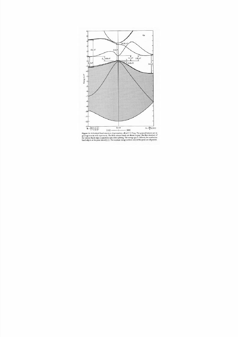
Figure 2.7: Energy vs. momentum diagram in three dimensions for
(a) GaAs and (b) Ge. The directions in the Brillouin zone are shown
in the inset and the letters indicate the position in momentum
space.
Note that the X point is the zone boundary along [100],
the L point along [111] and the K point along [110]. Γ is
the zero momentum point at the center of the Brillouin
zone where the electron wave has no momentum
8/14/2019 Chapter 2 THE PHYSICS OF SOLIDS
http://slidepdf.com/reader/full/chapter-2-the-physics-of-solids 25/122
8/14/2019 Chapter 2 THE PHYSICS OF SOLIDS
http://slidepdf.com/reader/full/chapter-2-the-physics-of-solids 26/122
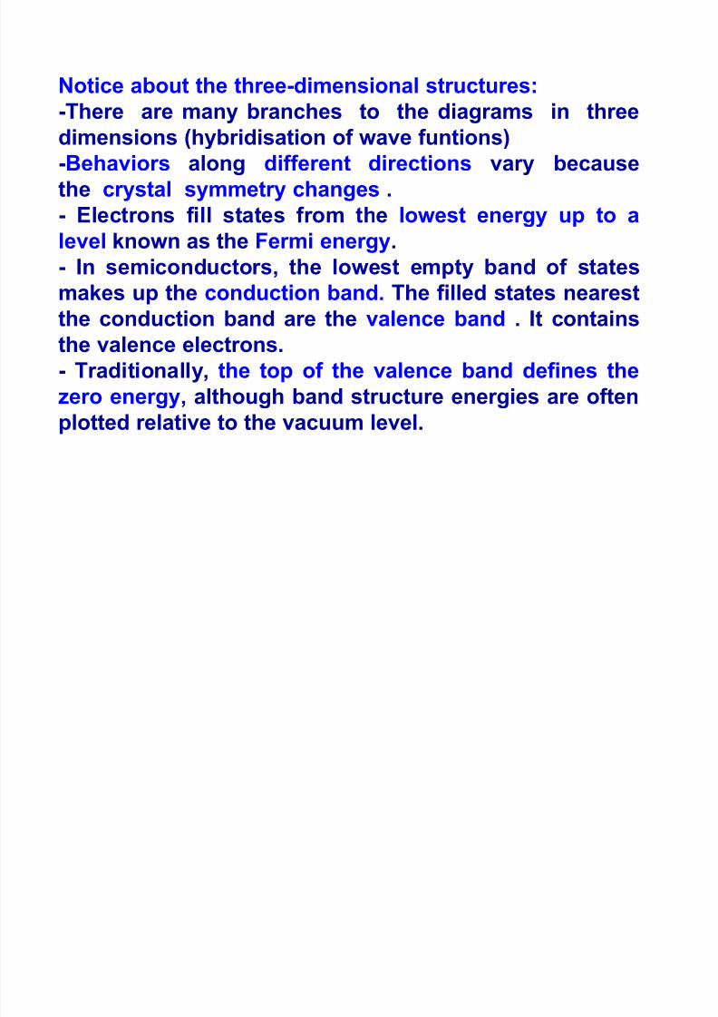
Notice about the three-dimensional structures:
-There are many branches to the diagrams in three
dimensions (hybridisation of wave funtions)
-Behaviors along different directions vary because
the crystal symmetry changes .- Electrons fill states from the lowest energy up to a
level known as the Fermi energy.
- In semiconductors, the lowest empty band of states
makes up the conduction band. The filled states nearestthe conduction band are the valence band . It contains
the valence electrons.
- Traditionally, the top of the valence band defines the
zero energy, although band structure energies are oftenplotted relative to the vacuum level.

8/14/2019 Chapter 2 THE PHYSICS OF SOLIDS
http://slidepdf.com/reader/full/chapter-2-the-physics-of-solids 27/122
• The minimum energy in the conduction band does not
necessarily occur at the same momentum as themaximum energy in the valence band. Therefore, an
electron at the conduction band minimum may not have
the same momentum as the electron in the valence band
maximum.
• When the conduction band minimum occurs at the same
momentum as the valence band maximum thesemiconductor is termed “direct” (Figure 2.7a)
• An “indirect” semiconductor has these extrema at
different momenta (Figure 2.7b).

8/14/2019 Chapter 2 THE PHYSICS OF SOLIDS
http://slidepdf.com/reader/full/chapter-2-the-physics-of-solids 28/122
2.1.5 Electrons and holes
Semiconductor or insulator: a gap between the filled andempty electronic states.
Charge can be carried either by electrons moving in the
normally empty states of the conduction band or by thehole moving in the normally filled states of the valence
band.
Holes are referred to as “quasi-particles” because they donot exist in isolation;
In a solid, holes appear to have charge and mass. Holes
can be treated as if they were real particles.
8/14/2019 Chapter 2 THE PHYSICS OF SOLIDS
http://slidepdf.com/reader/full/chapter-2-the-physics-of-solids 29/122
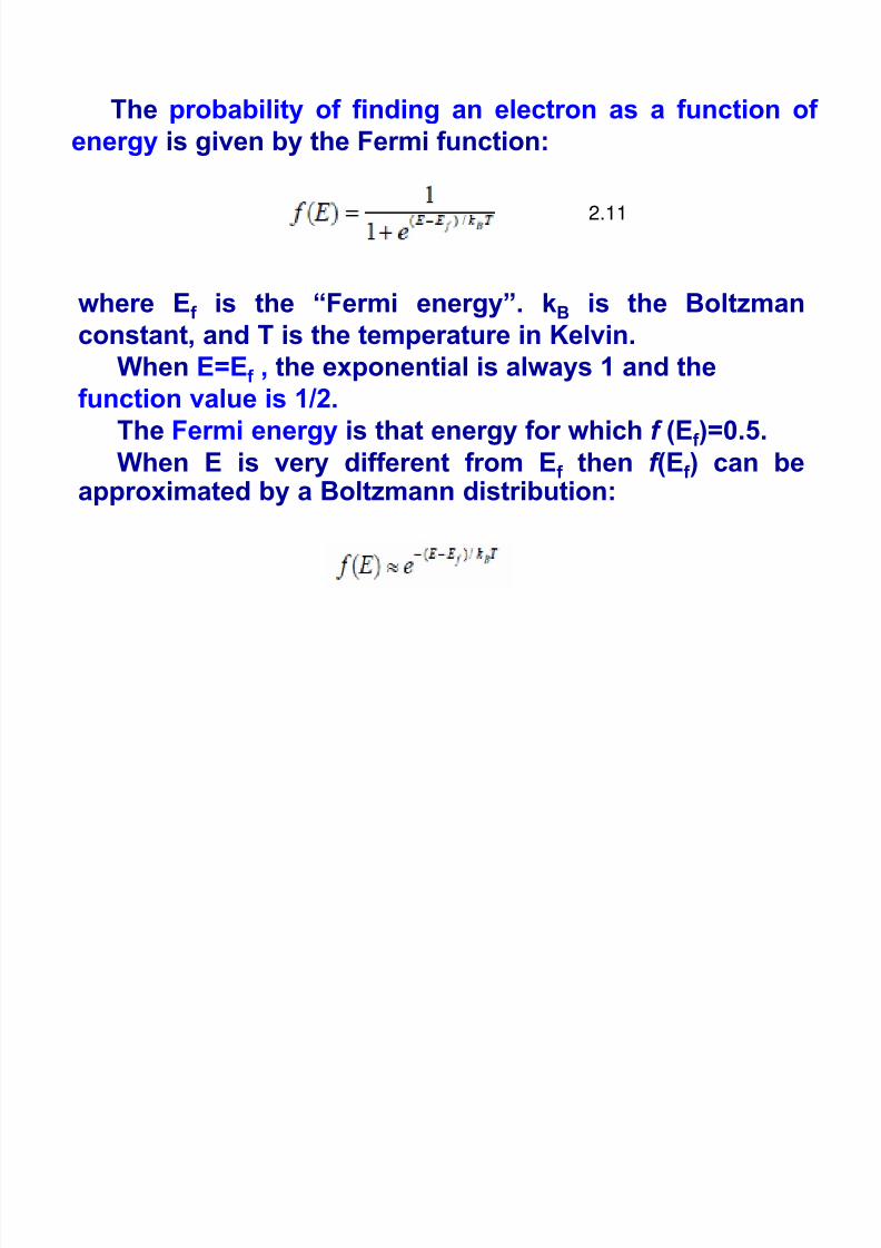
The probability of finding an electron as a function of
energy is given by the Fermi function:
where Ef is the “Fermi energy”. kB is the Boltzman
constant, and T is the temperature in Kelvin.
When E=Ef , the exponential is always 1 and thefunction value is 1/2.
The Fermi energy is that energy for which f (Ef )=0.5.
When E is very different from Ef then f (Ef ) can beapproximated by a Boltzmann distribution:
2.11

8/14/2019 Chapter 2 THE PHYSICS OF SOLIDS
http://slidepdf.com/reader/full/chapter-2-the-physics-of-solids 30/122

8/14/2019 Chapter 2 THE PHYSICS OF SOLIDS
http://slidepdf.com/reader/full/chapter-2-the-physics-of-solids 31/122
If the distribution of states were the same in the
conduction and valence bands and no states existed
within the energy gap, then charge neutrality would
require that the Fermi energy be near the gap center,
Generation of free carriers: Electrons are constantly
being transferred from the valence band to the conduction
band by energy absorption.
Thermal generation by absorption of energy from the
solid
Optical generation by absorption of external lightshining on the material

8/14/2019 Chapter 2 THE PHYSICS OF SOLIDS
http://slidepdf.com/reader/full/chapter-2-the-physics-of-solids 32/122
Recombination: Carriers (electrons) falling back
into the holes created by the earlier band- to-band
transfer
Radiative recombination releases lightHeat recombination (non-radiative recombination).
The thermal generation rate, gth,:
gth = Ce−(Eg / kB
T), 2.13
where Eg is energy gap of the material, C is a
proportionality constant.

8/14/2019 Chapter 2 THE PHYSICS OF SOLIDS
http://slidepdf.com/reader/full/chapter-2-the-physics-of-solids 33/122
Optical generation rate:
where G(ν) is the optical intensity at frequency ν, and Q(ν) function
of frequency related to the band structure and the optical
absorption coeffcient
Recombination depends upon the product of electron and hole densities and a factor of the
probability of a given recombination mechanism (for
example, radiative or non-radiative).
The recombination rate :
r rec = Q'np, 2.15
where Q’ is the a recombination rate per electron-hole
pair.Recombination occurs rapidly in direct-gap
semiconductors (Q’ large) and slowly in indirect-gap
semiconductors (Q’ small).
2.14

8/14/2019 Chapter 2 THE PHYSICS OF SOLIDS
http://slidepdf.com/reader/full/chapter-2-the-physics-of-solids 34/122
2.1.6 Direct and indirect semiconductors-The energy band structures of direct and indirect types of
semiconductor :
Figure 2.8: A schematic of the difference between a direct gap and an
indirect gap semiconductor.

8/14/2019 Chapter 2 THE PHYSICS OF SOLIDS
http://slidepdf.com/reader/full/chapter-2-the-physics-of-solids 35/122
The minimum energy of the conduction band in indirect
materials is at a different momentum than that of the
maximum energy of the valence band.
Electrons in the conduction band rapidly relax to the
minimum band energy.
Holes equally rapidly move to the maximum energy of the valence band.
Electrons and holes do not normally have the same
momentum in an indirect semiconductor while in a direct-
gap material these momenta are equal.Optical absorption /emission involves
absorption/creation of a photon with a consequent change
in energy of an electron, usually resulting in the transfer
of that electron to/from the conduction band from/to thevalence band.

8/14/2019 Chapter 2 THE PHYSICS OF SOLIDS
http://slidepdf.com/reader/full/chapter-2-the-physics-of-solids 36/122
For practical purposes one can assume that photons lead to
vertical transitions among bands on the E(k) diagram while
phonons make horizontal transitions
2121K K K qK phot ≈→=+
21E h E phot =+ ν
0 K
E
EC
EV
gE∆
0 K
gE∆
EC
E
EV
a b
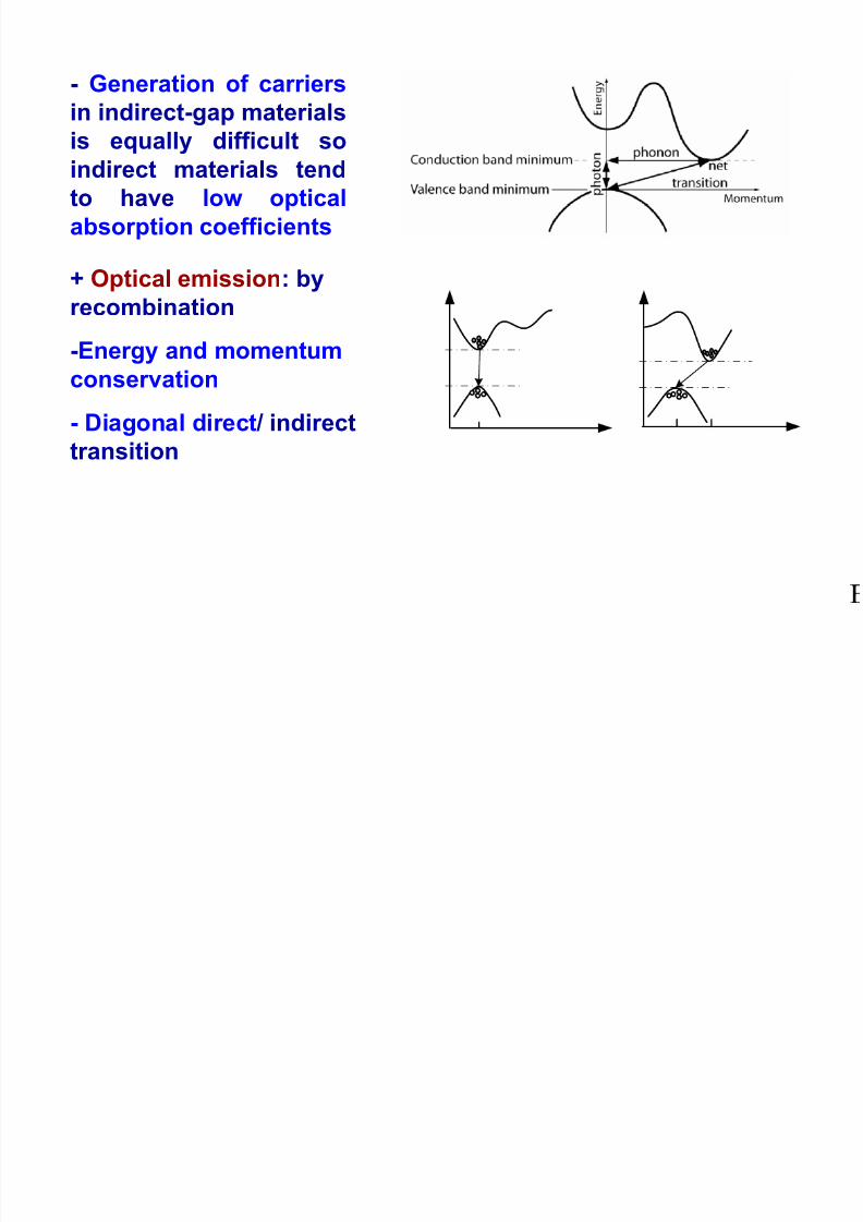
+ Optical absorption:
-Direct transition / Verticaltransition for direct
semiconductor
-Indirect transition /non-vertical transition for indirect
semiconductor: three particles (electron, phonon, andphoton) participating
21K qqK phon phot
=±+
21K qK phon
=±
21E h E phon phot =±+ ω ν
(photons have almost no momentum)
Phonons have a large momentum
gE∆
8/14/2019 Chapter 2 THE PHYSICS OF SOLIDS
http://slidepdf.com/reader/full/chapter-2-the-physics-of-solids 37/122
- Generation of carriers
in indirect-gap materials
is equally difficult so
indirect materials tend
to have low optical
absorption coefficients
+ Optical emission: by
recombination
-Energy and momentumconservation
- Diagonal direct / indirect
transition

8/14/2019 Chapter 2 THE PHYSICS OF SOLIDS
http://slidepdf.com/reader/full/chapter-2-the-physics-of-solids 38/122
2.1.7 Effective mass
The nearly-free electron model of solids shows thatelectrons are strongly affected by the lattice in which they
move.
The interaction of the electron with a solid modifies the
relationship between energy and momentum.
The change in kinetic energy with wavelength changes from
one material to another. In some materials the energy gain is
small for a given momentum increase. In others, it is larger for
the same added momentum.
The change in proportionality constant between energy and
momentum appears as a change in the effective mass of the
electron.
The energy of a free electron in the crystal is related to the
wave vector as:
where m* is the effective electron mass
Diff i i b h id i h k

8/14/2019 Chapter 2 THE PHYSICS OF SOLIDS
http://slidepdf.com/reader/full/chapter-2-the-physics-of-solids 39/122
Differentiating both sides with respect to k
Differentiating a second time
The effective mass of an electron Bloch wave is inverselyrelated to the curvature of the E(k) diagram.
Strong curvatures mean small effective masses and vice
versa.
The effective mass is generally expressed in units of electron mass in a vacuum, i.e. m*/m0.
The effective mass concept is only defined near a band
maximum or minimum where the energy can be approximated
as a quadratic function of wave vector, k.
Near a minimum in energy bands the E(k) function is
concave up and 1/m*>0
Near a maximum, 1/m*<0.
The effective mass near a maximum for holes is negative

8/14/2019 Chapter 2 THE PHYSICS OF SOLIDS
http://slidepdf.com/reader/full/chapter-2-the-physics-of-solids 40/122
2.1.8 Density of statesDensity of states: the number of states per unit energy in
the band structure.
For a free electron in three dimensions the energy is
given by
where kx, ky, and kz are the components of the wave vector k
along the three coordinate directions.
The longest wavelength or lowest energy state would
be a half wavelength across the entire width of the crystal, L.
Higher energy modes are integer multiples of this state.
The separation of states along any given direction: π /Li
The wave vector : ki=niπ /Li.
The energy can be rewritten :
where nx, ny and nz are the indices of the reciprocal lattice
points inside a sphere of radius kF

8/14/2019 Chapter 2 THE PHYSICS OF SOLIDS
http://slidepdf.com/reader/full/chapter-2-the-physics-of-solids 41/122
Sphere radius kF:
The lowest energy state of the system
The number of electrons that can be accommodated in states
with energy E:
Here the factor of two is because each state has two possibleelectron spins and the 1/8 is because we must take only
positive values of nx, ny, and nz.

8/14/2019 Chapter 2 THE PHYSICS OF SOLIDS
http://slidepdf.com/reader/full/chapter-2-the-physics-of-solids 42/122
The density of states g(E) per unit volume in an
energy interval dE :
g(E)= (1/V)(dN/dE),where V=L3 is the crystal volume (for a cube-shaped solid)
This density of states will apply to any band extremum
where the band has a quadratic dependence of energy
on momentum. It means for near a band edge.
The importance of the density of states:

8/14/2019 Chapter 2 THE PHYSICS OF SOLIDS
http://slidepdf.com/reader/full/chapter-2-the-physics-of-solids 43/122
-The importance of the density of states:
The calculation of the rate of any process in a solid, ;
Exam: absorption and emission of light.For any process to occur, an electron must be
present in an initial state with energy Ei and there must be
an empty state with energy Ef
Ef =Ei+∆E ∆E: energy change-The rate of such a process is given by “Fermi’s Golden Rule”.
-The rate of a process (H) moving an electron from state ψi to
state ψf :
where Ei and Ef are the initial and final state energies,
∆E is the change in energy of the process,gi and gf are the density of states at energies Ei and Ef ,
f(Ei) and f(Ef ) are the corresponding Fermi functions,
δ(Ei-Ef +∆E) is a Kroniker delta function
The expression <ψi|H|ψf > is a mathematical function which
enforces the conservation of momentum of the electrons .
2 2 INTRINSIC AND EXTRINSIC SEMICONDUCTORS

8/14/2019 Chapter 2 THE PHYSICS OF SOLIDS
http://slidepdf.com/reader/full/chapter-2-the-physics-of-solids 44/122
2.2 INTRINSIC AND EXTRINSIC SEMICONDUCTORS
-Semiconductors are called semiconductors because their
ability to conduct electricity is neither very great nor very small.-A semiconductor free of significant impurities is termed
“intrinsic” while those doped with impurities are termed
“extrinsic”.
2.2.1 Intrinsic semiconductors-An intrinsic semiconductor :
no impurities
the number of electrons, n, in the conduction band
exactly matches the number of holes, p, in the valence band:
n=p.-Intrinsic carrier concentration ni.
-Carrier concentration is given by the probability that a state at
energy E is filled , multiplied by the density of states at that
energy integrated over all energies at or above the conduction
band edge:
S b tit ti f E ti 2 11 d 2 22

8/14/2019 Chapter 2 THE PHYSICS OF SOLIDS
http://slidepdf.com/reader/full/chapter-2-the-physics-of-solids 45/122
Substituting from Equations 2.11 and 2.22:
The band edge energy is typically far from the Fermi energy
in units of kBT, in an intrinsic material , the Boltzmannapproximation can be used, then:
Where Nc is the effective density of states at the conduction band edge:
A similar for hole
ni=p,
NV : the effective valence-band density of states,

8/14/2019 Chapter 2 THE PHYSICS OF SOLIDS
http://slidepdf.com/reader/full/chapter-2-the-physics-of-solids 46/122
Taking the square-root gives a value for ni which does not depend
upon EF:
ni depends exponentially with temperature on half of thesemiconductor energy gap.
Narrow gap semiconductors will have large intrinsic carrier
concentrations while wide-gap materials will have fewer mobile
carriers at a given temperature.
As n=p=ni, the Fermi energy of an instrinsic semiconductor can be
derived:
The Fermi energy is near the middle of the energy gap and deviates
from the exact center by a factor that depends logarithmically on the
ratio of effective masses of the two bands and linearly on
temperature.
2.31
2.30
2.29

8/14/2019 Chapter 2 THE PHYSICS OF SOLIDS
http://slidepdf.com/reader/full/chapter-2-the-physics-of-solids 47/122
Figure 2.10: A plot of the electron concentration in a piece of silicon
doped with 1015 cm-3 donor atoms having an ionization energy of 0.04 eV.
The steep slope at high temperature (low inverse temperature)
corresponds to the intrinsic behavior for carriers crossing the energy
gap.
The lower temperature behavior occurs in the presence of the 1015 cm-3
electron donors. The slopes of the two curves correspond to the 1.1 eV
energy gap and the 0.04 eV donor ionization energies, respectively.
2 2 2 Extrinsic semiconductors

8/14/2019 Chapter 2 THE PHYSICS OF SOLIDS
http://slidepdf.com/reader/full/chapter-2-the-physics-of-solids 48/122
2.2.2 Extrinsic semiconductors
-When impurities are added to a semiconductor the
bonding pattern in that semiconductor is modified.
-Impurities that are added intentionally to control the
carrier concentrations are called “dopants”.-When a dopant has the same basic electronic structure as
the atom it replaces (for example, partially-filled “s” and
“p” orbitals for dopants in Si), the bonding behavior is
substantially unchanged.-The extra electron or hole can often escape the impurity
atom and move freely through the semiconductor causing
a change in conductivity
-Acceptor dopant : the dopant atom has one fewer electronthan the host
-Donor dopant: the dopant atom has one extra electron
than the host.
8/14/2019 Chapter 2 THE PHYSICS OF SOLIDS
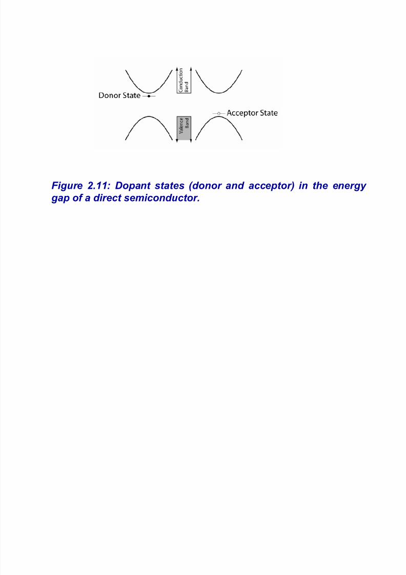
http://slidepdf.com/reader/full/chapter-2-the-physics-of-solids 49/122
Figure 2.11: Dopant states (donor and acceptor) in the energy
gap of a direct semiconductor.
-Electrons or holes in these dopant states can be easily

8/14/2019 Chapter 2 THE PHYSICS OF SOLIDS
http://slidepdf.com/reader/full/chapter-2-the-physics-of-solids 50/122
-Electrons or holes in these dopant states can be easily
released into the bands : energy to transfer a carrier from
the dopant state to the band edge is small
-The probability of finding a carrier is calculated based on the
Fermi function and the separation of the dopant state from the
band edge.
For donors:
For hole:
Assuming the Fermi energy is at EA or ED,
ED and EA are the donor and acceptor energies,
EC and EV are the conduction and valence band edge energies,
ND and NA are the concentrations of donors and acceptors,
respectively.

8/14/2019 Chapter 2 THE PHYSICS OF SOLIDS
http://slidepdf.com/reader/full/chapter-2-the-physics-of-solids 51/122
-It is typical to assume that all dopant atoms areionized in a semiconductor at room temperature.
However, this is not the case.
-From the above equations, Dopant level lies kBT
from the band edge, only 27% of dopant atoms are
typically ionized.
Energy difference is half of kBT, only 38% are
ionized.

8/14/2019 Chapter 2 THE PHYSICS OF SOLIDS
http://slidepdf.com/reader/full/chapter-2-the-physics-of-solids 52/122
-When one adds dopant to a pure semiconductor theFermi level shifts, approaching the doping state
energy.
-if the Fermi energy rises in the band gap, the
concentration of holes in the valence band mustshrink.
-The intrinsic condition : n=p
np=ni
2
-Doping a semiconductor with an electron donor
increases the concentration of free electrons and
decreases the concentration of free holes by the
same factor.Electrons are called “majority carriers”
Holes are “minority carriers”.
-Acceptor doping : holes are the majority carrier

8/14/2019 Chapter 2 THE PHYSICS OF SOLIDS
http://slidepdf.com/reader/full/chapter-2-the-physics-of-solids 53/122
2.3 PROPERTIES AND THE BAND STRUCTURE
8/14/2019 Chapter 2 THE PHYSICS OF SOLIDS
http://slidepdf.com/reader/full/chapter-2-the-physics-of-solids 54/122
2.3 PROPERTIES AND THE BAND STRUCTURE
2.3.1 Resistance, capacitance, and inductance-Resistance, R, capacitance, C, and inductance, L, are
used in circuit elements.
-They result from the motion of electrons in solids andtheir interaction with each other and with the atoms
surrounding them.
-Each also depends upon the geometry of the circuit
element producing the effect.- The basic materials properties, however, are
dependent only upon the electronic structure in that
material and not on the geometry:
The resistivity, ρ, of a conducting material in a resistor,
The dielectric constant, ε, of the insulating material in a
capacitor
The permeability, µΒ, in an inductor
The relationships :

8/14/2019 Chapter 2 THE PHYSICS OF SOLIDS
http://slidepdf.com/reader/full/chapter-2-the-physics-of-solids 55/122
p
Where l is the length of the conductor and A is its cross-
sectional area.
The resistivity, ρ, of a conductor is inversely related toits conductivity, σ as ρ=1/σ.
A is the area of the capacitor plates and d is their
separation or the thickness of the insulating
(dielectric) material between them.
Th i d t lt f th fl f t d

8/14/2019 Chapter 2 THE PHYSICS OF SOLIDS
http://slidepdf.com/reader/full/chapter-2-the-physics-of-solids 56/122
-The inductance results from the flow of current around
a loop or coil of wire.-The magnetic field produced depends upon the
permeability of the material inside the wire coil.
-The greater the energy stored in the magnetic field, the
higher the inductance of the coil.The inductance of a solenoid depends upon the
permeability as:
where N is the number of turns of wire in the coil, A
is the coil area, and l is the coil length.
2.3.1.1 Mobility and electrical conductivityConduction in solids can occur by motion of electrons or

8/14/2019 Chapter 2 THE PHYSICS OF SOLIDS
http://slidepdf.com/reader/full/chapter-2-the-physics-of-solids 57/122
-Conduction in solids can occur by motion of electrons or
ions: Electronic conduction
Ionic conduction.
-Ionic conduction occurs by diffusion ionized atoms, generally
at high temperatures,Fast ionic conductors are used as solid electrolytes in
fuel cells (replacements for batteries) and sensors.
-Electronic conductivity: motion of electrons ands holes
When a material is placed in an electric field, E, acurrent density, J, is given:
J=σE,The electrical conductivity σ of semiconductor:
where q is the moving carrier charge, µn and µp are the electron and
hole mobilities, and n and p are the electron and hole mobile carrier
concentrations.
-In a metal, the number of carriers moving depends upon the
d it f i th F i

8/14/2019 Chapter 2 THE PHYSICS OF SOLIDS
http://slidepdf.com/reader/full/chapter-2-the-physics-of-solids 58/122
density of carriers near the Fermi energy.
-The effective density of mobile carriers in a metal : thenumber of carriers within kBT of the Fermi energy, of the order
of one per atom or >>1022 cm-3.
-When an electron is placed in an electric field, it accelerates.
The acceleration:a = qE/m
where m is the mass of the moving carrier.
-The “drift” velocity
vd = aττ : the average time between collisions
- The quantity qτ /m* is the carrier mobility, µn or µp.
-The two variable components of mobility

8/14/2019 Chapter 2 THE PHYSICS OF SOLIDS
http://slidepdf.com/reader/full/chapter-2-the-physics-of-solids 59/122
the mean time between collisions
the effective mass of the moving charge.-Three primary scattering centers
The electrons,
The atoms of the solid,
Defects in a crystal.
-The first two are generally determined by fundamental
properties of the material,
-The latter is controlled by the density of imperfections.-Scattering of electrons may be estimated from Fermi’s
Golden Rule
The more electrons scattering into the moving charge and
the larger the number of states the moving carrier canscatter into, the higher the scattering rate and the shorter
the mean time between scattering events.

8/14/2019 Chapter 2 THE PHYSICS OF SOLIDS
http://slidepdf.com/reader/full/chapter-2-the-physics-of-solids 60/122
-In metal, when g(Ef ) is high there are many carriers toscatter from with energies just below Ef and many states
to scatter into just above Ef .
-Metals such as Mo have low conductivities because
they have high densities of states around Ef .
-Metals such as Cu, Ag, and Au have high enough
carrier densities for good conduction but low enough
densities of states to keep the mean scattering timeslong (less scattering)

8/14/2019 Chapter 2 THE PHYSICS OF SOLIDS
http://slidepdf.com/reader/full/chapter-2-the-physics-of-solids 61/122

8/14/2019 Chapter 2 THE PHYSICS OF SOLIDS
http://slidepdf.com/reader/full/chapter-2-the-physics-of-solids 62/122
- The mobility can be connected to the diffusivity of a
carrier.Einstein showed that the mobility multiplied by the
thermal energy (kBT) is equal to the charge multiplied by
the diffusivity.
For electron:
This relationship is most useful in balancing the
diffusion current of electrons or holes due to the
concentration gradient against a drift current due to an
electric field and is essential to understanding the
behavior of diodes.
2.3.1.2 Dielectric constant, piezoelectric response, and
bilit

8/14/2019 Chapter 2 THE PHYSICS OF SOLIDS
http://slidepdf.com/reader/full/chapter-2-the-physics-of-solids 63/122
permeability
The dielectric constant of materials directly is related totheir ability to be polarized
Polarizability is related to the magnitude of the motion of
charge in a material resulting in the accumulation of
negative charge in the material at the positive end of the
external electric field and positive charge at the negative
end .
This increases the field strength outside and decreasesit inside the dielectric.
The increased field strength around the edges of the
dielectric increases charge accumulation in surrounding
materials, resulting in more capacitance.

8/14/2019 Chapter 2 THE PHYSICS OF SOLIDS
http://slidepdf.com/reader/full/chapter-2-the-physics-of-solids 64/122
Figure 2.12: A schematic diagram showing the
response of a dielectric material to an applied
electric field.
The redistribution of charge resulting from the applied

8/14/2019 Chapter 2 THE PHYSICS OF SOLIDS
http://slidepdf.com/reader/full/chapter-2-the-physics-of-solids 65/122
g g
field, E, results in a “displacement” field, D within amaterial :D = E + 4πP =εE ,
where ε is dielectric constant:
ε=ε0εr ,ε0=8.85x10⁻¹⁴ F cm-1 is the permittivity of free space and
εr is the relative dielectric constant of the material .
P is the polarizability of the material.
The dielectric constant can be written in terms of the
polarizability of the solid as:
ε = (1+ 4πP /E ).

8/14/2019 Chapter 2 THE PHYSICS OF SOLIDS
http://slidepdf.com/reader/full/chapter-2-the-physics-of-solids 66/122
The total polarizability is represented in terms of the
polarization, p, of a unit cell volume v , as:
More field produces more polarization.
The field-independent materials property is the
polarizability per unit cell, α, :
p = αElocal.
Elocal is the electric field inside the material that produces
the polarization of the unit cell.
P = p/v
Two contributions to the polarizability, α, :
atomic polarizability

8/14/2019 Chapter 2 THE PHYSICS OF SOLIDS
http://slidepdf.com/reader/full/chapter-2-the-physics-of-solids 67/122
atomic polarizability
displacement polarizability.The atomic polarizability is caused by the motion of the electron cloud
in the material with respect to the ionic cores of the atoms on lattice
sites.
The displacement polarizability is the motions of charged atoms with
respect to one another. There be two or more types of atoms in thelattice having a net polarity or difference in electric charge and results
from motion of the negative atoms with respect to the positive atoms.
Figure 2.13: A schematic diagram
showing the two major components to
polarizability. In atomic polarizability, the
electron cloud is displaced with respect to
the remaining positive components of the
atoms (the protons and the non-valence
electrons). In displacement polarizability,
atoms of different charge (positive or
negative) with respect to their average
charge.
The polarization behavior resulting from atomic polarizability can be
estimated by representing the electron cloud as a negatively-charged
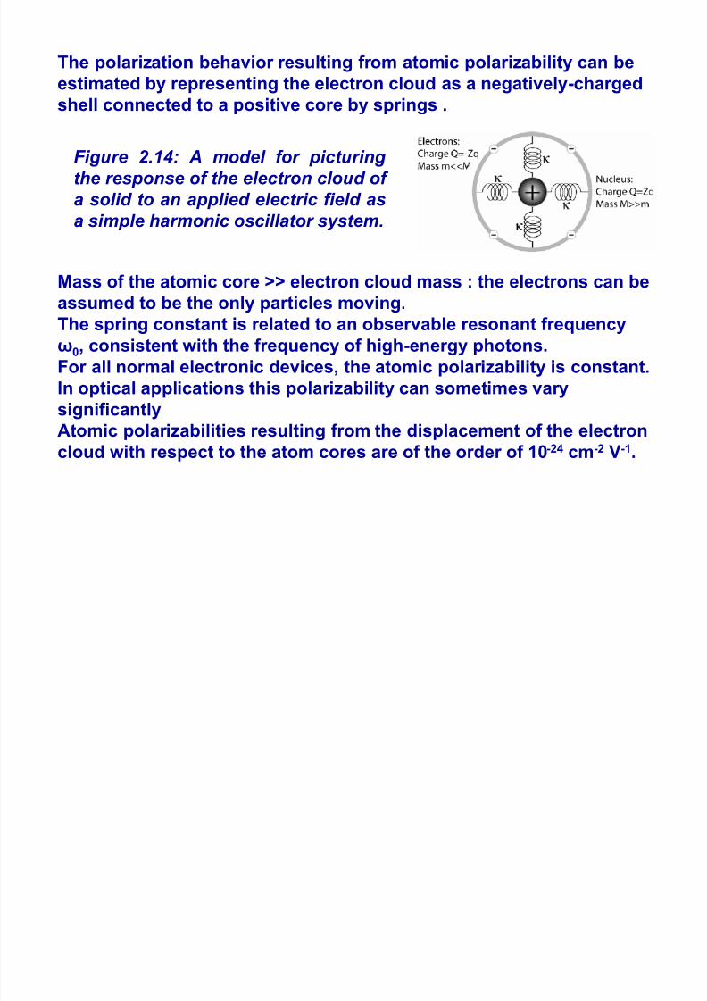
8/14/2019 Chapter 2 THE PHYSICS OF SOLIDS
http://slidepdf.com/reader/full/chapter-2-the-physics-of-solids 68/122
y p g g y g
shell connected to a positive core by springs .
Mass of the atomic core >> electron cloud mass : the electrons can be
assumed to be the only particles moving.The spring constant is related to an observable resonant frequency
ω0, consistent with the frequency of high-energy photons.
For all normal electronic devices, the atomic polarizability is constant.
In optical applications this polarizability can sometimes varysignificantly
Atomic polarizabilities resulting from the displacement of the electron
cloud with respect to the atom cores are of the order of 10-24 cm-2 V-1.
Figure 2.14: A model for picturing
the response of the electron cloud of
a solid to an applied electric field asa simple harmonic oscillator system.
The displacement polarizability results from motion of heavy atoms
with respect to each other.

8/14/2019 Chapter 2 THE PHYSICS OF SOLIDS
http://slidepdf.com/reader/full/chapter-2-the-physics-of-solids 69/122
p
These particles being much more massive than electronsThey respond to fields much more slowly.
The same general model of masses connected by springs can be
applied.
The displacement polarizability :
M+ and M- are the masses of the positively and negatively-charged
ions, Z is the average ionic charge in units of electron charge (q), ω is
the frequency of the applied electric field, and is the resonantfrequency of the system.
When : very large polarizability and consequently a large
change in dielectric constant.
For normal materials the resonant frequency is near the “Debyefrequency” . The resonant energy of these vibrations is typically 10-
100 meV, or of the order of kBT at room temperature.
Thus, the displacement polarizability of partially ionic crystals
becomes frequency-dependent for photons in the infrared portion of
the optical spectrum.
The general trends in dielectric response of materials:
The atomic polarizability:

8/14/2019 Chapter 2 THE PHYSICS OF SOLIDS
http://slidepdf.com/reader/full/chapter-2-the-physics-of-solids 70/122
The atomic polarizability:
• increases with the number of valence electrons;• increases with decreasing binding energy for valence
electrons around atoms (this changes the “spring constant”
and lowers the resonant frequency).
The displacement polarizability:
• requires charge transfer among atoms in the unit cell (atomic
solids and those without charge transfer show no displacement
polarizability) so more ionic materials have a larger
polarizability;• larger displacements and “softer” crystals increase
displacement dielectric
constant.
-Piezoelectric materials:

8/14/2019 Chapter 2 THE PHYSICS OF SOLIDS
http://slidepdf.com/reader/full/chapter-2-the-physics-of-solids 71/122
-Piezoelectric materials:
Partially ionic material that lacks a center of inversionsymmetry,
Displacement of atoms of one polarity with respect to
atoms of another polarity results in a change in shape of the
material ( an applied field induces a shape change)- A relationship between shape and applied electric field is
termed a “piezoelectric” response.
- An example: all zincblende-structure materials are
piezoelectric.
In these materials, a cation and anion lie at opposite ends of each bond and the structure is not symmetric around this bond.
All bond pairs are oriented in the same way. Therefore, the
structure lacks an inversion symmetry.
-Piezoelectric behavior can work as a shape change canproduce an electric field.
8/14/2019 Chapter 2 THE PHYSICS OF SOLIDS
http://slidepdf.com/reader/full/chapter-2-the-physics-of-solids 72/122
The permeability of a material is tied to its ability to be magnetized .
The magnetic response of a material depends upon the arrangement

8/14/2019 Chapter 2 THE PHYSICS OF SOLIDS
http://slidepdf.com/reader/full/chapter-2-the-physics-of-solids 73/122
The magnetic response of a material depends upon the arrangement
of electrons in the atoms of that material.Electrons have a “spin” of which is related to their intrinsic
magnetic moment of .
When the spin vectors of the electrons in an atom align, the atom
has a higher magnetic moment.The ability of electron spins to align is limited by quantum state
availability.
Half-filled states allow any combination of spins and high magnetic
response, while completely filled states allow only one combination
of antiparallel spins.When the spins of separate atoms align parallel to each other the
system develops a net magnetization in local domains.
A sufficiently large applied field can align the magnetic fields of the
domains with the external field resulting in a net magnetization.If this field persists after removal of the applied field the material is a
ferromagnet.
-Paramagnet material : the spins within atoms or molecules do not
align spontaneously from atom/molecule to atom/molecule . Such
alignment can be induced by an applied field

8/14/2019 Chapter 2 THE PHYSICS OF SOLIDS
http://slidepdf.com/reader/full/chapter-2-the-physics-of-solids 74/122
alignment can be induced by an applied field.
-Antiferromagnetic materials: spins among atoms are spontaneously
align opposite to one another.
-The permeability of ferromagnets is of the order of hundreds to
hundreds of thousands,
-Paramagnets have values greater than unity by 10-10,000 parts per million,
-Diamagnets have permeabilities smaller than unity by one to 200
parts per million.
2.3.2 Optical properties-The absorption, transmission, and reflection of light all depend

8/14/2019 Chapter 2 THE PHYSICS OF SOLIDS
http://slidepdf.com/reader/full/chapter-2-the-physics-of-solids 75/122
critically on the density of states and Fermi energy in a material.-Transparent materials have a gap in the density of states around the
Fermi energy such that there are no states available into which an
electron absorbing a photon could move.
Figure 2.15: A schematic representation of the density of states of a
metal which would lead to strong absorption in a limited range of
energies and weak absorption at other energies.
A large density of electrons and states available near Ef , allows
electrons to move in response to electromagnetic waves causing
their reflection In this case the material appears colored (as in Cu or

8/14/2019 Chapter 2 THE PHYSICS OF SOLIDS
http://slidepdf.com/reader/full/chapter-2-the-physics-of-solids 76/122
their reflection. In this case the material appears colored (as in Cu or
Au).
Material has an energy gap (or very low density of states) between
filled and empty levels, allows light with energy below the gap
energy to pass through the material. Transparent materials have
very large energy gaps.Examples of transparent materials : silicon dioxide (as in window
glass) and aluminum oxide (which is colored by impurities to make
ruby and several other gemstones).
The emission of light: a large density of electrons in a band with
high energy (for example the conduction band) and holes at a lower
energy (such as in the valence band).
The liberated energy may be emitted in the form of light.
The dielectric constant has a strong effect on optical properties
2.3.3 Thermal properties
- Variety of thermal properties of materials : heat capacity, thermal

8/14/2019 Chapter 2 THE PHYSICS OF SOLIDS
http://slidepdf.com/reader/full/chapter-2-the-physics-of-solids 77/122
conductivity, thermal expansion coefficient, etc..To focus on the thermal conductivity as it is critical to many
electronic devices.
The thermal conductivity, κ, of a material results from transport of
energy via electrons or via lattice vibrations (phonons).
The total thermal conductivity :
2.3.3.1 Heat Conduction by Phonons
"Phonon" is the name given to a cooperative vibration of atoms in
a crystalline lattice

8/14/2019 Chapter 2 THE PHYSICS OF SOLIDS
http://slidepdf.com/reader/full/chapter-2-the-physics-of-solids 78/122
a crystalline lattice
Phonons for making transitions between minimum-energy
states of indirect-gap semiconductors.
Phonon: Primary reservoir of thermal energy in most solids and
therefore contribute to thermal conduction.
Phonons are sound waves with a wavelength of the order of the lattice constant in the solid.
The number of phonon modes is limited by the physical
dimensions of the solid and the number of atoms
A typical phonon dispersion relation for a one-dimensional
solid : Figure 2.16: Phonon dispersion
relation for a one-dimensional lattice
of balls connected by springs. On the
long-wavelength “acoustic” branch
atoms move as groups in one directionor another with the direction varying
over relatively long distances. For the
higher-energy “optical” branch atoms
move in opposite directions over
very short distances.
The energy of the average phonon in a solid at equilibrium is the
average thermal energy of an atom in that solid, kBT.

8/14/2019 Chapter 2 THE PHYSICS OF SOLIDS
http://slidepdf.com/reader/full/chapter-2-the-physics-of-solids 79/122
Therefore, the distribution of phonons estimated by the modeenergies and the temperature of the solid.
Phonons travel at the speed of sound.
To conduct heat by phonon motion, the phonons scatter in the
solid and come to equilibrium with the local temperature of the
lattice.The phonon (lattice vibration) contribution to thermal conductivity:
CV is the heat capacity of the solid at constant volume, is the
average speed of sound, and Λ is the mean free path of phonons
between scattering events.The mean free path for phonons decreases as the number of
phonons present in the solid increases due to a higher scattering
probability.

8/14/2019 Chapter 2 THE PHYSICS OF SOLIDS
http://slidepdf.com/reader/full/chapter-2-the-physics-of-solids 80/122
Figure 2.17: The phonon dispersion relations for (a) GaN and (b) Si
TA, LA, LO, and TO refer to transverse acoustic, longitudinal
acoustic, longitudinal optical and transverse optical phonons,
respectively. Longitudinal modes run along bonds as in Figure 2.16,while for transverse modes the vibration velocity is
perpendicular to the bonds.
There are two transverse modes because there are two axes
perpendicular to a bond direction.
-The phonon mean free path in a typical solid :

8/14/2019 Chapter 2 THE PHYSICS OF SOLIDS
http://slidepdf.com/reader/full/chapter-2-the-physics-of-solids 81/122
where c is a constant.
Phonon-related contributions to the thermal conductivity through Λ
and through CV.
At higher temperatures , the heat capacity is simply determined
by vibrations of individual atoms.Each atom has three independent vibrational modes, one for
each direction in space, and each mode has an average
energy kBT.
The heat capacity is, by definition, ∂E/∂T from which:
where Θ is called the Debye temperature.
- At low temperatures the heat capacity is also related to the Debye
temperature :
N is the number of particles vibrating per unit volume (the atomic
density) and the factor of three results from the three independent
coordinates of vibration direction.
-Insulators: no free electrons
only phonons transmit heat.

8/14/2019 Chapter 2 THE PHYSICS OF SOLIDS
http://slidepdf.com/reader/full/chapter-2-the-physics-of-solids 82/122
y p
-Thermal conductivity of such a material is relatively low value
-Most electrical insulators are relatively good thermal insulators.
-The notable exception is diamond with the highest thermal
conductivity of any material.
In common applications, electrical insulators are also used as heatinsulators.
The best thermal insulators are amorphous materials, which have
lower thermal conductivities because phonons cannot exist over
extended ranges.
The scattering distance for phonons becomes one atomic spacing.
In this case the transmission of heat in the material becomes a
process of diffusion of energy among loosely coupled harmonic
oscillators.
In the high temperature, the minimum thermal conductivity :

8/14/2019 Chapter 2 THE PHYSICS OF SOLIDS
http://slidepdf.com/reader/full/chapter-2-the-physics-of-solids 83/122
-The value for SiO2 is ~0.01 W/cm•K,
-Thus, amorphous silica (glass) is a nearly perfect
thermal insulator.
-Improvement of thermal insulator : to decrease thedensity of the glass.
-For example: The heat shielding tiles on the space
shuttle make use of underdense fiberous silica to
achieve an exceptionally low thermal conductivity.
2.3.3.2 Heat Conduction by Electrons
Electrons come to thermal equilibrium with the lattice when they
scatter.

8/14/2019 Chapter 2 THE PHYSICS OF SOLIDS
http://slidepdf.com/reader/full/chapter-2-the-physics-of-solids 84/122
Electrons transport heat well:They easily move through the lattice of a conductive solid
with relatively long mean-free path lengths.
The electron contribution to thermal conductivity is:
where Celec, νelec, and Λelec are the heat capacity, mean velocity, and
mean free path of electrons near the Fermi energy in the solid.
The thermal conductivity of electrons depends in thetemperature, T, and the electrical conductivity, σ, of the material:
the Wiedemann-Franz law. L is a constant.
For a free electron solid L~2.45x10⁻⁸ WΩ /K2
In real metals, L ranges from ~2.2 to 3.0 x10⁻⁸ WΩ /K2
In general, the thermal conductivity of electrons is much greater than
for phonons.
-Artificial-potential-barrier structures appear in a number of
2.4 QUANTUM WELLS & CONFINED CARRIERS

8/14/2019 Chapter 2 THE PHYSICS OF SOLIDS
http://slidepdf.com/reader/full/chapter-2-the-physics-of-solids 85/122
important microelectronic device applications: the laser diode.-Laser diodes consist of a series of layers that are designed to
collect electrons and holes.
-Recombination of the free carriers in the trap leads to exceptionally
efficient laser light emission.
-The trap is a potential well resulting from the sandwiching of anarrow-gap semiconductor between two layers of wider-gap
material.
-Discontinuities in the valence and conduction band edges
produce a lower-potential region where the carriers tend tocollect.
-Because these wells are of the size scale of an electron wave
function, the quantum nature of the system determines its
properties.
-Such structures are known as quantum wells.
To consider a potential well with infinite side walls

8/14/2019 Chapter 2 THE PHYSICS OF SOLIDS
http://slidepdf.com/reader/full/chapter-2-the-physics-of-solids 86/122
The potential :
U=0 for |x| < L
U=∞
for |x|≥
L.
The solution to Schrödinger for |x| ≥ L must be ψ(x) = 0.
For |x| < L the equation is (in one dimension):
Figure 2.18: (a) a potential
well with infinite walls.
where
The solutions are proportional to sin(κx) and cos(κx).
Wave function is zero outside the well
Th f ti i id d t id t t h t th b d i

8/14/2019 Chapter 2 THE PHYSICS OF SOLIDS
http://slidepdf.com/reader/full/chapter-2-the-physics-of-solids 87/122
The wave function inside and outside must match at the boundariesκL = nπ, where n=1,2,3,… for the sin(κx) solution
κL = (n-1/2)π for cos(κx)
Nodes at the walls of the well
Figure 2.19: Electron states in an infinite-depth quantum well. Note
that these are simply harmonics of the fundamental mode with nodes
at the edges of the well.
A finite well :
Figure 2.18: (b) a well
f d th U ll h

8/14/2019 Chapter 2 THE PHYSICS OF SOLIDS
http://slidepdf.com/reader/full/chapter-2-the-physics-of-solids 88/122
To consider the solutions of the Schrödinger equation for particleswith energies below the energy of the edges of the well.
U=0 for |x|≥L
U=-U0 for |x|<L.
The solutions:
of depth, U 0 . well has awidth of 2L.
The two exponential relationships describe the decay of the wave
function outside of the well,
The middle relationship describes the wave function within the well.
-The wave function and its first derivative must be continuous
across the well boundaries.
-The boundary conditions yield four equations (two boundaries,
hi di i ) i f k (A B C D)

8/14/2019 Chapter 2 THE PHYSICS OF SOLIDS
http://slidepdf.com/reader/full/chapter-2-the-physics-of-solids 89/122
two matching conditions) in four unknowns (A,B,C,D)
The second two formulas in Equation 2.57 are from boundary conditionmatching.
The first part is the bound state requirement and can be rewritten:

8/14/2019 Chapter 2 THE PHYSICS OF SOLIDS
http://slidepdf.com/reader/full/chapter-2-the-physics-of-solids 90/122
The bound state energy lies below the well boundary
and is harmonic-oscillator-like.
the energy to be zero at the bottom of the well: the solutions become
simple free-electron waves within the well as in Equation 2.16.Because the bound states must be standing waves in the well (must
have a maximum or a zero at the well center), the values of k are
linked to the well half-width, L.
The constraint:
This equation: connection between the wave length, the well width,
the well depth
The well dimenssion determines the wavelength and energy of the
states within the welll
2.59

8/14/2019 Chapter 2 THE PHYSICS OF SOLIDS
http://slidepdf.com/reader/full/chapter-2-the-physics-of-solids 91/122
Figure 2.20: Solutions to the Schrödinger equation given by
2.55 and subject to the additional conditions of Equations 2.56-
2.59.
The important points from these equations:
-Equation 2.59 shows that the possible values of the wavelength, k
are coupled to the well half width L and to the depth of the well

8/14/2019 Chapter 2 THE PHYSICS OF SOLIDS
http://slidepdf.com/reader/full/chapter-2-the-physics-of-solids 92/122
are coupled to the well half width, L, and to the depth of the well.-Deeper wells produce more bound states with slightly shorter
wavelengths (as the wave function is less inclined to penetrate the
well sides).
-Wider wells produce more bound states for a given well depth.-There are very few states in the well and these have discrete
energies.
-There are no states at the bottom of the well as would be judged
from the band edges. Therefore, the band gap of the well is greater
than the minimum gap of the semiconductor from which it isproduced.
-The wave function decays exponentially in the barriers with a
decay length κ that increases with decreasing well depth.
-The wave function penetrates the surrounding barriers asignificant distance. This gives rise to coupling between adjacent
quantum wells.
Two quantum wells close enough to each other :
the tails of their wave functions can overlap significantly

8/14/2019 Chapter 2 THE PHYSICS OF SOLIDS
http://slidepdf.com/reader/full/chapter-2-the-physics-of-solids 93/122
the tails of their wave functions can overlap significantlyThey can be coupled together.
The interaction of their wave functions alters the energies of
states in the wells.
This interaction produces:bonding-like pairs and raised in energy
antibonding-like pairs of states, lowered in energy.
An infinite number of coupled wells would produce a band of
states in each well associated with each quantum state for a
single well.The widths of the bands are directly related to the well-to-well
coupling.
Well coupling depends upon the depth of the well and
exponentially upon the distance between the wells.

8/14/2019 Chapter 2 THE PHYSICS OF SOLIDS
http://slidepdf.com/reader/full/chapter-2-the-physics-of-solids 94/122
Figure 2.21: An example semiconductor superlattice structure
resulting in quantum wells as shown for the conduction band
edge. Similar but shallower wells occur in the valence
band. The bound states in the wells are also indicated.
These states overlap producing splitting and multiple levels in
each well
A wells depth U0=200 meV, a well width 2L = 4 nm, a well
separation s = 4 nm.
A series of quantum wells produced by growth of 4 nm thick

8/14/2019 Chapter 2 THE PHYSICS OF SOLIDS
http://slidepdf.com/reader/full/chapter-2-the-physics-of-solids 95/122
A series of quantum wells produced by growth of 4 nm thickAl0.19Ga0.81As layers alternating with 4 nm thick GaAs layers in a
superlattice.
The GaAs layers produce the wells
The Al0.19
Ga0.81
As provides the barriers.
The states in the quantum wells couple with each other such that
the first-nearest neighbor wells have two states rather than the
single state that a single well would have.
These states change their energies by ~10 meV relative to the
single well.Second nearest neighbor interactions when three or more wells are
present cause additional splitting with a further change of energy
of ~4.5 meV, and so on.
The result is a series of states in the quantum well at the center of
the superlattice with energies
The more quantum wells that are coupled together the more
states occur in each well and the closer together these states are.

8/14/2019 Chapter 2 THE PHYSICS OF SOLIDS
http://slidepdf.com/reader/full/chapter-2-the-physics-of-solids 96/122
Figure 2.22: A plot of the number of states and their energies in a
quantum well which interacts with the specified number of other identical wells. An essentially infinite superlattice produces a band
of states as indicated.
-Impotant points to notice about Figure 2.22. :
First, the states increase in energy more than they decrease
because as a state drops in the quantum well, the energy barrierseparating those states from their neighbors rises Consequently
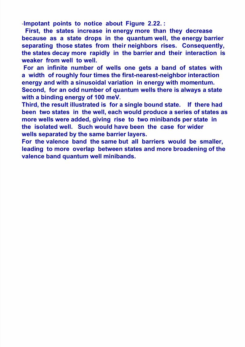
8/14/2019 Chapter 2 THE PHYSICS OF SOLIDS
http://slidepdf.com/reader/full/chapter-2-the-physics-of-solids 97/122
because as a state drops in the quantum well, the energy barrier separating those states from their neighbors rises. Consequently,
the states decay more rapidly in the barrier and their interaction is
weaker from well to well.
For an infinite number of wells one gets a band of states with
a width of roughly four times the first-nearest-neighbor interactionenergy and with a sinusoidal variation in energy with momentum.
Second, for an odd number of quantum wells there is always a state
with a binding energy of 100 meV.
Third, the result illustrated is for a single bound state. If there hadbeen two states in the well, each would produce a series of states as
more wells were added, giving rise to two minibands per state in
the isolated well. Such would have been the case for wider
wells separated by the same barrier layers.
For the valence band the same but all barriers would be smaller,leading to more overlap between states and more broadening of the
valence band quantum well minibands.
Each state in the quantum well can accommodate electrons
or holes and can give rise to absorption and emission of

8/14/2019 Chapter 2 THE PHYSICS OF SOLIDS
http://slidepdf.com/reader/full/chapter-2-the-physics-of-solids 98/122
g plight.
In laser diodes : advantage of single quantum wells to trap
electrons and holes to enhance recombination.
It is important to use only single quantum wells or widely-separated wells to prevent broadening of the states
Such broadening would give rise to a range of emission
wavelengths.

8/14/2019 Chapter 2 THE PHYSICS OF SOLIDS
http://slidepdf.com/reader/full/chapter-2-the-physics-of-solids 99/122

8/14/2019 Chapter 2 THE PHYSICS OF SOLIDS
http://slidepdf.com/reader/full/chapter-2-the-physics-of-solids 100/122

8/14/2019 Chapter 2 THE PHYSICS OF SOLIDS
http://slidepdf.com/reader/full/chapter-2-the-physics-of-solids 101/122

8/14/2019 Chapter 2 THE PHYSICS OF SOLIDS
http://slidepdf.com/reader/full/chapter-2-the-physics-of-solids 102/122

8/14/2019 Chapter 2 THE PHYSICS OF SOLIDS
http://slidepdf.com/reader/full/chapter-2-the-physics-of-solids 103/122

8/14/2019 Chapter 2 THE PHYSICS OF SOLIDS
http://slidepdf.com/reader/full/chapter-2-the-physics-of-solids 104/122

8/14/2019 Chapter 2 THE PHYSICS OF SOLIDS
http://slidepdf.com/reader/full/chapter-2-the-physics-of-solids 105/122

8/14/2019 Chapter 2 THE PHYSICS OF SOLIDS
http://slidepdf.com/reader/full/chapter-2-the-physics-of-solids 106/122

8/14/2019 Chapter 2 THE PHYSICS OF SOLIDS
http://slidepdf.com/reader/full/chapter-2-the-physics-of-solids 107/122

8/14/2019 Chapter 2 THE PHYSICS OF SOLIDS
http://slidepdf.com/reader/full/chapter-2-the-physics-of-solids 108/122

8/14/2019 Chapter 2 THE PHYSICS OF SOLIDS
http://slidepdf.com/reader/full/chapter-2-the-physics-of-solids 109/122

8/14/2019 Chapter 2 THE PHYSICS OF SOLIDS
http://slidepdf.com/reader/full/chapter-2-the-physics-of-solids 110/122

8/14/2019 Chapter 2 THE PHYSICS OF SOLIDS
http://slidepdf.com/reader/full/chapter-2-the-physics-of-solids 111/122

8/14/2019 Chapter 2 THE PHYSICS OF SOLIDS
http://slidepdf.com/reader/full/chapter-2-the-physics-of-solids 112/122

8/14/2019 Chapter 2 THE PHYSICS OF SOLIDS
http://slidepdf.com/reader/full/chapter-2-the-physics-of-solids 113/122

8/14/2019 Chapter 2 THE PHYSICS OF SOLIDS
http://slidepdf.com/reader/full/chapter-2-the-physics-of-solids 114/122

8/14/2019 Chapter 2 THE PHYSICS OF SOLIDS
http://slidepdf.com/reader/full/chapter-2-the-physics-of-solids 115/122

8/14/2019 Chapter 2 THE PHYSICS OF SOLIDS
http://slidepdf.com/reader/full/chapter-2-the-physics-of-solids 116/122

8/14/2019 Chapter 2 THE PHYSICS OF SOLIDS
http://slidepdf.com/reader/full/chapter-2-the-physics-of-solids 117/122

8/14/2019 Chapter 2 THE PHYSICS OF SOLIDS
http://slidepdf.com/reader/full/chapter-2-the-physics-of-solids 118/122

8/14/2019 Chapter 2 THE PHYSICS OF SOLIDS
http://slidepdf.com/reader/full/chapter-2-the-physics-of-solids 119/122

8/14/2019 Chapter 2 THE PHYSICS OF SOLIDS
http://slidepdf.com/reader/full/chapter-2-the-physics-of-solids 120/122

8/14/2019 Chapter 2 THE PHYSICS OF SOLIDS
http://slidepdf.com/reader/full/chapter-2-the-physics-of-solids 121/122

8/14/2019 Chapter 2 THE PHYSICS OF SOLIDS
http://slidepdf.com/reader/full/chapter-2-the-physics-of-solids 122/122