chapter 2: structural modelingocw.snu.ac.kr/sites/default/files/note/6627.pdf · chapter 2:...
TRANSCRIPT
Chapter 2: Structural Modeling
Digital System Designs and Practices Using Verilog HDL and FPGAs @ 2008, John Wiley 2-1
Chapter 2: Structural Modeling
Prof. Soo-Ik Chae

Chapter 2: Structural Modeling
Digital System Designs and Practices Using Verilog HDL and FPGAs @ 2008, John Wiley 2-2
Objectives
After completing this chapter, you will be able to:
Describe what is the structural modeling
Describe how to instantiate gate primitives
Describe how to model a design in gate primitives
Describe inertial and transport delays
Describe how to specify delays in gates
Describe hazards and their effects in gate networks
Chapter 2: Structural Modeling
Digital System Designs and Practices Using Verilog HDL and FPGAs @ 2008, John Wiley 2-3
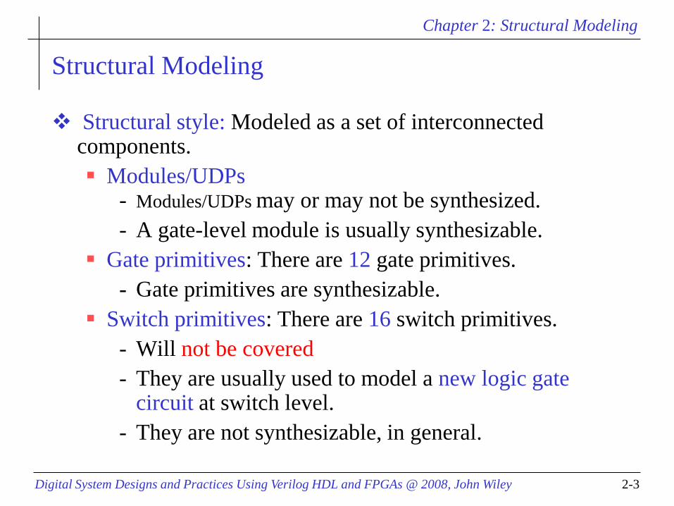
Structural Modeling
Structural style: Modeled as a set of interconnected components.
Modules/UDPs- Modules/UDPs may or may not be synthesized.
- A gate-level module is usually synthesizable.
Gate primitives: There are 12 gate primitives.
- Gate primitives are synthesizable.
Switch primitives: There are 16 switch primitives.
- Will not be covered
- They are usually used to model a new logic gate circuit at switch level.
- They are not synthesizable, in general.
Chapter 2: Structural Modeling
Digital System Designs and Practices Using Verilog HDL and FPGAs @ 2008, John Wiley 2-4
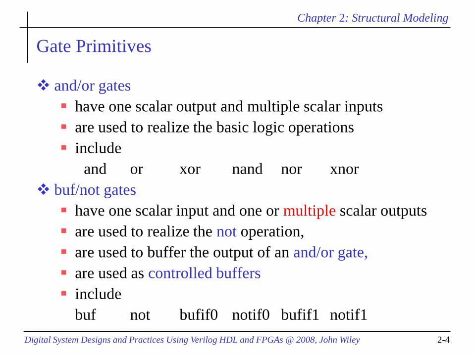
Gate Primitives
and/or gates
have one scalar output and multiple scalar inputs
are used to realize the basic logic operations
include
and or xor nand nor xnor
buf/not gates
have one scalar input and one or multiple scalar outputs
are used to realize the not operation,
are used to buffer the output of an and/or gate,
are used as controlled buffers
include
buf not bufif0 notif0 bufif1 notif1

Chapter 2: Structural Modeling
Digital System Designs and Practices Using Verilog HDL and FPGAs @ 2008, John Wiley 2-5
and/nand Gates
0 1 x z
0
1
x
z
i2and
i1
0 0 0 0
0 1 x x
0 x x x
0 x x x
0 1 x z
0
1
x
z
i2nand
i1
1 1 1 1
1 0 x x
1 x x x
1 x x x
i1i2
i1i2out out

Chapter 2: Structural Modeling
Digital System Designs and Practices Using Verilog HDL and FPGAs @ 2008, John Wiley 2-6
or/nor Gates
0 1 x z
0
1
x
z
i2or
i1
0 1 x x
1 1 1 1
x 1 x x
x 1 x x
0 1 x z
0
1
x
z
i2nor
i1
1 0 x x
0 0 0 0
x 0 x x
x 0 x x
i1i2
i1i2out out
Chapter 2: Structural Modeling
Digital System Designs and Practices Using Verilog HDL and FPGAs @ 2008, John Wiley 2-7
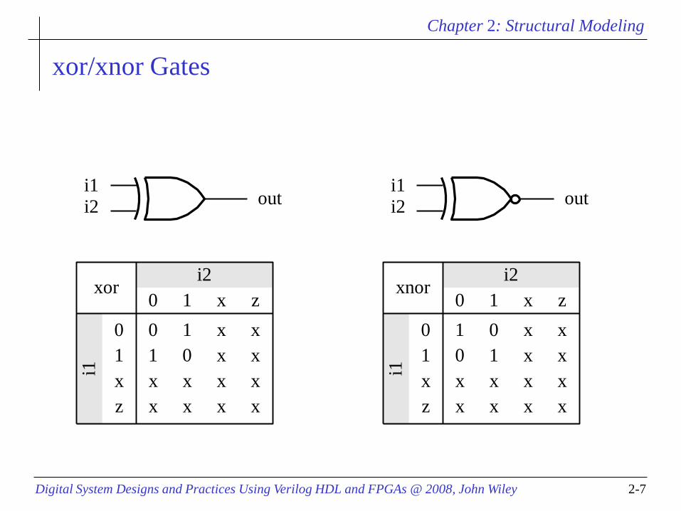
xor/xnor Gates
0 1 x z
0
1
x
z
i2xor
i1
0 1 x x
1 0 x x
x x x x
x x x x
0 1 x z
0
1
x
z
i2xnor
i1
1 0 x x
0 1 x x
x x x x
x x x x
i1i2
i1i2out out
Chapter 2: Structural Modeling
Digital System Designs and Practices Using Verilog HDL and FPGAs @ 2008, John Wiley 2-8
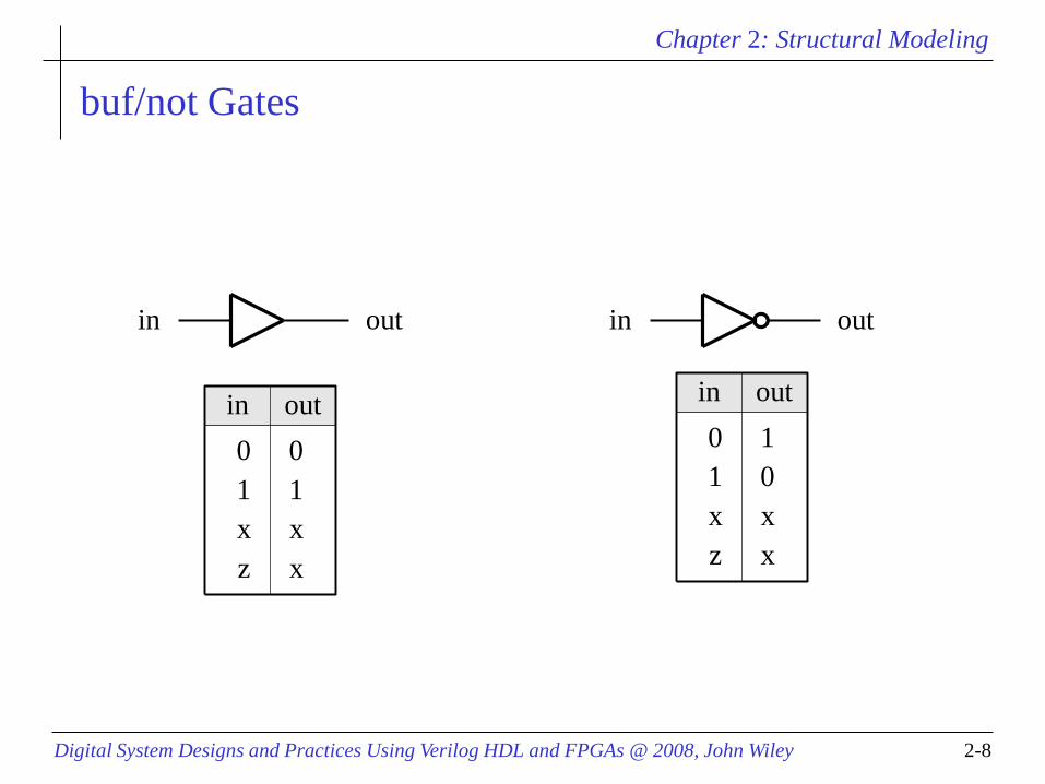
buf/not Gates
in outin out
0
1
x
z
outin
0
1
x
x
0
1
x
z
outin
1
0
x
x
Chapter 2: Structural Modeling
Digital System Designs and Practices Using Verilog HDL and FPGAs @ 2008, John Wiley 2-9
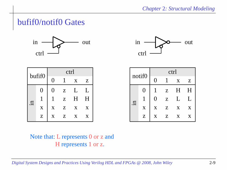
bufif0/notif0 Gates
in out
ctrl
in out
ctrl
0 1 x z
0
1
x
z
ctrlnotif0
in
1 z H H
0 z L L
x z x x
x z x x
0 1 x z
0
1
x
z
ctrlbufif0
in
0 z L L
1 z H H
x z x x
x z x x
Note that: L represents 0 or z and
H represents 1 or z.
Chapter 2: Structural Modeling
Digital System Designs and Practices Using Verilog HDL and FPGAs @ 2008, John Wiley 2-10
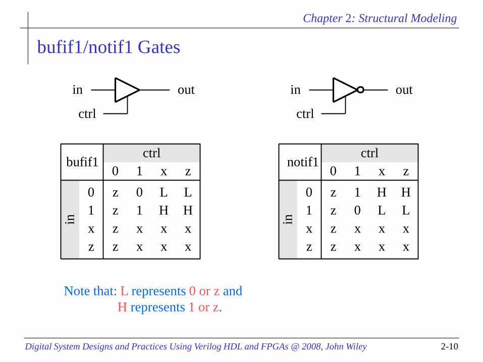
bufif1/notif1 Gates
0 1 x z
0
1
x
z
ctrlnotif1
in
z 1 H H
z 0 L L
z x x x
z x x x
in out
ctrl
in out
ctrl
0 1 x z
0
1
x
z
ctrlbufif1
in
z 0 L L
z 1 H H
z x x x
z x x x
Note that: L represents 0 or z and
H represents 1 or z.

Chapter 2: Structural Modeling
Digital System Designs and Practices Using Verilog HDL and FPGAs @ 2008, John Wiley 2-11
Instantiation of Basic Gates
To instantiate and/or gates
instance_name is optional.
gatename [instance_name](output, input1, input2, ..., inputn);
x
y
z
fa
b
c
g1
g2
g3
g4
module basic_gates (x, y, z, f) ;
input x, y, z;
output f ;
wire a, b, c; // internal nets
// Structural modeling using basic gates.
nor g1 (b, x, y);
not g2 (a, x);
and g3 (c, a, z);
nor g4 (f, b, c);
endmodule

Chapter 2: Structural Modeling
Digital System Designs and Practices Using Verilog HDL and FPGAs @ 2008, John Wiley 2-12
Array of Instances
Array instantiations may be a synthesizer dependent!
Suggestion: you had better to check this feature before
using the synthesizer.
wire [3:0] out, in1, in2;
// basic array instantiations of nand gate.
nand n_gate[3:0] (out, in1, in2);
// this is equivalent to the following:
nand n_gate0 (out[0], in1[0], in2[0]);
nand n_gate1 (out[1], in1[1], in2[1]);
nand n_gate2 (out[2], in1[2], in2[2]);
nand n_gate3 (out[3], in1[3], in2[3]);

Chapter 2: Structural Modeling
Digital System Designs and Practices Using Verilog HDL and FPGAs @ 2008, John Wiley 2-13
An Example --- A 1-Bit Full Adder
module full_adder_structural(x, y, c_in, s, c_out);
// I/O port declarations
input x, y, c_in;
output s, c_out;
wire s1, c1, c2, c3;
// Structural modeling of the 1-bit full adder.
xor xor_s1(s1, x, y); // compute sum.
xor xor_s2(s, s1, c_in);
and and_c1(c1, x, y); // compute carry out.
and and_c2(c2, x, c_in);
and and_c3(c3, y, c_in);
or or_cout(c_out, c1, c2, c3);
endmodule
y
c_ins
x
c_out
s1
c1
c2
c3
Chapter 2: Structural Modeling
Digital System Designs and Practices Using Verilog HDL and FPGAs @ 2008, John Wiley 2-14
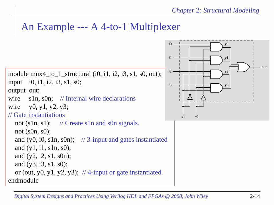
An Example --- A 4-to-1 Multiplexer
module mux4_to_1_structural (i0, i1, i2, i3, s1, s0, out);
input i0, i1, i2, i3, s1, s0;
output out;
wire s1n, s0n; // Internal wire declarations
wire y0, y1, y2, y3;
// Gate instantiations
not (s1n, s1); // Create s1n and s0n signals.
not (s0n, s0);
and (y0, i0, s1n, s0n); // 3-input and gates instantiated
and (y1, i1, s1n, s0);
and (y2, i2, s1, s0n);
and (y3, i3, s1, s0);
or (out, y0, y1, y2, y3); // 4-input or gate instantiated
endmodule
i0
i1
outi2
i3
s1 s0
y0
y1
y2
y3
Chapter 2: Structural Modeling
Digital System Designs and Practices Using Verilog HDL and FPGAs @ 2008, John Wiley 2-15
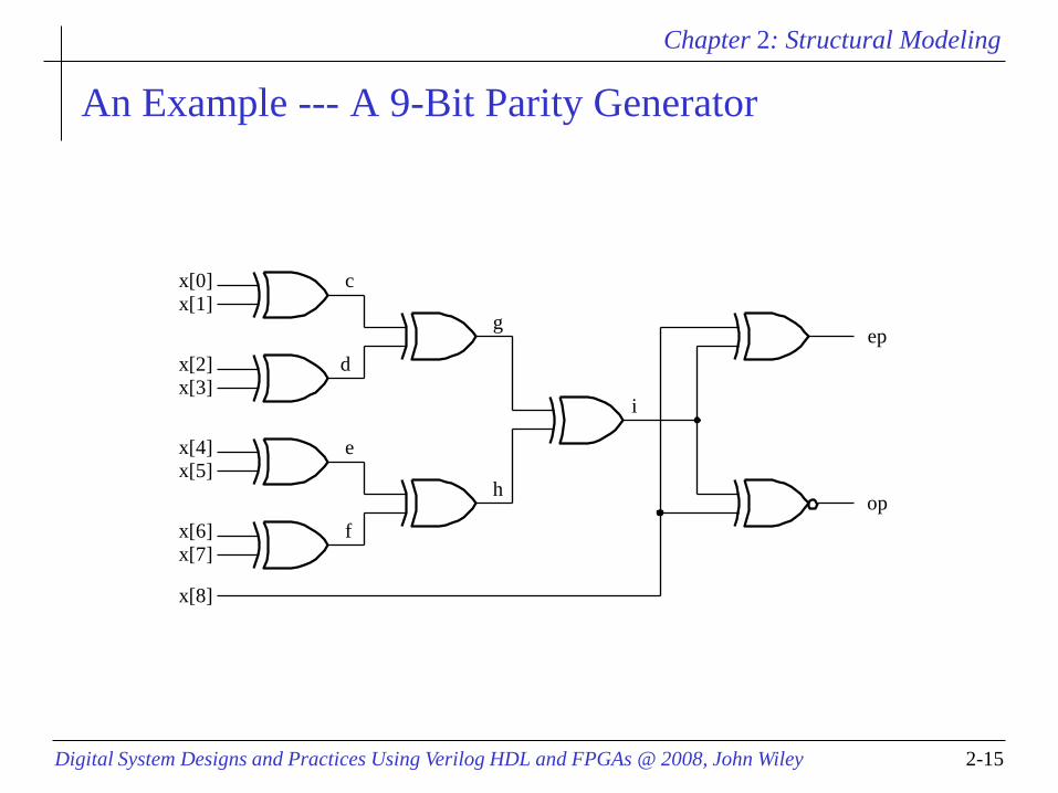
An Example --- A 9-Bit Parity Generator
cx[0]
ep
op
x[1]
x[2]
x[3]
x[4]
x[5]
x[6]
x[7]
x[8]
d
e
f
g
h
i

Chapter 2: Structural Modeling
Digital System Designs and Practices Using Verilog HDL and FPGAs @ 2008, John Wiley 2-16
An Example --- A 9-Bit Parity Generator
module parity_gen_9b_structural(x, ep, op);
// I/O port declarations
input [8:0] x;
output ep, op;
wire c, d, e, f, g, h, j;
xor xor_11(c, x[0], x[1]); // first level
xor xor_12(d, x[2], x[3]);
xor xor_13(e, x[4], x[5]);
xor xor_14(f, x[6], x[7]);
xor xor_21(g, c, d); // second level
xor xor_22(h, e, f);
xor xor_31(i, g, h); // third level
xor xor_ep(ep, i, x[8]); // fourth level
xnor xnor_op(op, i, x[8]);
endmodule
Chapter 2: Structural Modeling
Digital System Designs and Practices Using Verilog HDL and FPGAs @ 2008, John Wiley 2-17
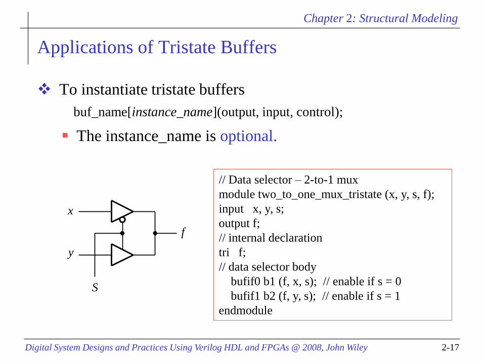
Applications of Tristate Buffers
To instantiate tristate buffers
The instance_name is optional.
// Data selector – 2-to-1 mux
module two_to_one_mux_tristate (x, y, s, f);
input x, y, s;
output f;
// internal declaration
tri f;
// data selector body
bufif0 b1 (f, x, s); // enable if s = 0
bufif1 b2 (f, y, s); // enable if s = 1
endmodule
x
f
y
S
buf_name[instance_name](output, input, control);

Chapter 2: Structural Modeling
Digital System Designs and Practices Using Verilog HDL and FPGAs @ 2008, John Wiley 2-18
Inertial and Transport Delay Models
Inertial delay model
The signal events do not persist long enough will not be
propagated to the output.
It is used to model gate delays (RC delays).
It is the default delay model for HDL (Verilog HDL and
VHDL).
Transport delay model
Any signal events will be propagated to the output.
It is used to model net (i.e. wires) delays.
The default delay of a net is zero.

Chapter 2: Structural Modeling
Digital System Designs and Practices Using Verilog HDL and FPGAs @ 2008, John Wiley 2-19
The Effects of Inertial Delays
wire a;
and #4 (b, x, y); // Inertial delay
and #4 (a, x, y);
not #1 (f, a);
x
yf
a
b
a
b
f
x
y
42 6 8 10 12 14 16 18 20
42 6 8 10 12 14 16 18 20
42 6 8 10 12 14 16 18 20
42 6 8 10 12 14 16 18 20
42 6 8 10 12 14 16 18 20Inertial delay
Chapter 2: Structural Modeling
Digital System Designs and Practices Using Verilog HDL and FPGAs @ 2008, John Wiley 2-20
The Effects of Transport and Inertial Delays
x
yf
a
b
wire #2 a; // Transport delay
and #4 (b, x, y); // Inertial delay
and #4 (a, x, y);
not #1 (f, a); a
b
f
x
y
42 6 8 10 12 14 16 18 20
42 6 8 10 12 14 16 18 20
42 6 8 10 12 14 16 18 20
42 6 8 10 12 14 16 18 20
42 6 8 10 12 14 16 18 20
Inertial delay
Transport delay

Chapter 2: Structural Modeling
Digital System Designs and Practices Using Verilog HDL and FPGAs @ 2008, John Wiley 2-21
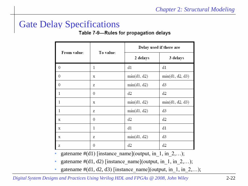
Gate Delay Specifications
Gate Delay Specifications
Specify propagation delay only:
• gatename #(prop_delay) [instance_name](output, in_1, in_2,…);
Specify both rise and fall times:
• gatename #(t_rise, t_fall) [instance_name](output, in_1, in_2,…);
Specify rise, fall, and turn-off times:
• gatename #(t_rise, t_fall, t_off) [instance_name](output, in_1,
in_2,…);
• Turn-off time: transition to high-impedance value
• When a value changes to x, the delay is the smallest of the two or
three delays
Delay specifier: min:typ:max
Chapter 2: Structural Modeling
Digital System Designs and Practices Using Verilog HDL and FPGAs @ 2008, John Wiley 2-22
Gate Delay Specifications
• gatename #(d1) [instance_name](output, in_1, in_2,…);
• gatename #(d1, d2) [instance_name](output, in_1, in_2,…);
• gatename #(d1, d2, d3) [instance_name](output, in_1, in_2,…);

Chapter 2: Structural Modeling
Digital System Designs and Practices Using Verilog HDL and FPGAs @ 2008, John Wiley 2-23
Gate Delays Specifications
// Only specify one delay
and #(5) a1 (b, x, y);
// Only specify one delay using min:typ:max
not #(10:12:15) n1 (a, x);
// Specify two delays using min:typ:max
and #(10:12:15, 12:15:20) a2 (c, a, z);
// Specify three delays using min:typ:max
or #(10:12:15, 12:15:20, 12:13:16) o2 (f, b, c);

Chapter 2: Structural Modeling
Digital System Designs and Practices Using Verilog HDL and FPGAs @ 2008, John Wiley 2-24
Hazards and Their Effects
A hazard is an unwanted short-width output signal when the
inputs to a combinational circuit changes.
These unwanted signals are generated when different paths
from input to output have different propagation delays.
Static hazard
Dynamic hazard
(b)static-0 hazard
10 01
(a) static-1 hazard
0 1
(c) dynamic hazard
0 1 0 1 1 0 1 0

Chapter 2: Structural Modeling
Digital System Designs and Practices Using Verilog HDL and FPGAs @ 2008, John Wiley 2-25
A Static Hazard Example
module hazard_static (x, y, z, f);
input x, y, z;
output f;
// internal declaration
wire a, b, c; // internal net
// logic circuit body
and #5 a1 (a, x, y);
not #5 n1 (c, x);
and #5 a2 (b, c, z);
or #5 o2 (f, b, a);
endmodule
x
y
x'
z
a
b
f
t pd
t pd
t pd
t pd
t pd
t pd
t pd
t pd
t pd
t pd
t pd
Hazard
x
y
z
f
a
bc

Chapter 2: Structural Modeling
Digital System Designs and Practices Using Verilog HDL and FPGAs @ 2008, John Wiley 2-26
A Dynamic Hazard Example
w
a
b
f
c
d
e
dynamic hazard
x = y = z = 1
x
z
f
2
1w
y
3
a
b
c
d
e