chapter 2 characteristics of physical op-amps - ece users pages
TRANSCRIPT

Chapter 2
Characteristics of Physical Op-Amps
In the preceding chapter, the op-amp is treated as an ideal circuit element. Because the waveform of theoutput voltage from a physical op-amp is never exactly the same as the waveform that would be expectedfrom an ideal op-amp, this assumption is never true in practice. Although most op-amp circuits can bedesigned by assuming that the op-amps are ideal, the circuits never perform exactly as predicted becauseof the non-ideal characteristics of the op-amps. Some of these characteristics are discussed in this chapter.In addition, a linear controlled-source model of the op-amp is developed which can be used in computersimulation programs such as SPICE.
2.1 Effects of Finite Gain and Bandwidth
2.1.1 Open-Loop Transfer Function
In our analysis of op-amp circuits this far, we have considered the op-amps to have an infinite gain andan infinite bandwidth. This is not true for physical op-amps. In this section, we examine the effects of anon-infinite gain and non-infinite bandwidth on the inverting and the non-inverting amplifier circuits. Fig.2.1 shows the circuit symbol of an op-amp having an open-loop voltage-gain transfer function A (s). Theoutput voltage is given by
Vo = A (s) (V+ − V−) (2.1)
where complex variable notation is used. We assume here that A (s) can be modeled by a single-pole low-passtransfer function of the form
A (s) =A0
1 + s/ω0(2.2)
where A0 is the dc gain constant and ω0 is the pole frequency. Most general purpose op-amps have avoltage-gain transfer function of this form for frequencies such that |A (jω)| ≥ 1.
Figure 2.1: Op-amp symbol.
i

ii CHAPTER 2 CHARACTERISTICS OF PHYSICAL OP-AMPS
2.1.2 Gain-Bandwidth Product
Figure 2.2 shows the Bode magnitude plot for A (jω). The radian gain-bandwidth product is defined as thefrequency ωx for which |A (jω)| = 1. It is given by
ωx = ω0
√A20 − 1 A0ω0 (2.3)
where we assume that A0 >> 1. This equation illustrates why ωx is called a gain-bandwidth product.It is given by the product of the dc gain constant A0 and the radian bandwidth ω0. It is commonlyspecified in Hz with the symbol fx, where fx = ωx/2π. Many general purpose op-amps have a gain-bandwidth product fx 1MHz and a dc gain constant A0 2 × 10⁵. It follows from Eq. (2.3) thatthe corresponding pole frequency in the voltage-gain transfer function for the general purpose op-amp isf0 1× 10⁶/
(2× 10⁵
)= 5Hz.
Figure 2.2: Bode plot of |A (jω)|.
2.1.3 Non-Inverting Amplifier
Figure 2.3 shows the circuit diagram of a non-inverting amplifier. For this circuit, we can write by inspection
Vo = A (s) (Vi − V−) (2.4)
V− = VoR1
R1 +RF(2.5)
Simultaneous solution for the voltage-gain transfer function yields
VoVi
=A (s)
1 +A (s)R1/ (R1 +RF )=
1 +RF/R11 + (1 +RF /R1) /A (s)
(2.6)
For s = jω and |(1 +RF/R1) /A (jω)| << 1, this reduces to Vo/Vi (1 +RF/R1). This is the gain whichwould be predicted if the op-amp is assumed to be ideal.
When Eq. (2.2) is used for A (s), it is straightforward to show that Eq. (2.6) can be written
VoVi
=A0f
1 + s/ω0f(2.7)
where A0f is the gain constant with feedback and ω0f is the radian pole frequency with feedback. These aregiven by
A0f =A0
1 +A0R1/ (R1 +RF )=
1 +RF/R11 + (1 +RF/R1) /A0
(2.8)

2.1. EFFECTS OF FINITE GAIN AND BANDWIDTH iii
Figure 2.3: Non-inverting amplifier.
ω0f = ω0
(1 +
A0R1R1 +RF
)(2.9)
It follows from these two equations that the radian gain-bandwidth product of the non-inverting amplifierwith feedback is given by A0fω0f = A0ω0 = ωx. This is the same as for the op-amp without feedback. Fig.2.4 shows the Bode magnitude plots for both Vo/Vi and A (jω). The figure shows that the break frequencyon the plot for Vo/Vi lies on the negative-slope asymptote of the plot for A (jω).
Figure 2.4: Bode plot for |Vo/Vi|.
Example 1 At very low frequencies, an op-amp has the frequency independent open-loop gain A (s) = A0 =2× 10⁵. The op-amp is to be used in a non-inverting amplifier. The theoretical gain is calculated assumingthat the op-amp is ideal. What is the highest theoretical gain that gives an error between the theoretical gainand the actual gain that is less than 1%?
Solution. The theoretical gain is given by (1 +RF /R1). The actual gain is always less than the theoreticalgain. For an error less than 1%, we can use Eq. (2.6) to write
1− 0.01 <1
1 + (1 +RF/R1) / (2× 10⁵)
This can be solved for the upper bound on the theoretical gain to obtain
1 +RFR1
< 2× 10⁵(
1
0.99− 1
)= 2020

iv CHAPTER 2 CHARACTERISTICS OF PHYSICAL OP-AMPS
Example 2 An op-amp has a gain-bandwidth product of 1MHz. The op-amp is to be used in a non-invertingamplifier circuit. Calculate the highest gain that the amplifier can have if the half-power or −3 dB bandwidthis to be 20 kHz or more.
Solution. The minimum bandwidth occurs at the highest gain. For a bandwidth of 20 kHz, we can writeA0f × 20× 103 = 106. Solution for A0f yields A0f = 50.
Example 3 Two non-inverting op-amp amplifiers are operated in cascade. Each amplifier has a gain of 10.If each op-amp has a gain-bandwidth product of 1MHz, calculate the half-power or −3dB bandwidth of thecascade amplifier.
Solution. Each amplifier by itself has a pole frequency of 106/10 = 100 kHz, corresponding to a radianfrequency ω0f = 2π × 100, 000. The cascade combination has the voltage-gain transfer function given by
VoVi
= 100
(1
1 + s/ω0f
)2
The half-power frequency is obtained by setting s = jω and solving for the frequency for which |Vo/Vi|2 =1002/2. If we let x = ω/ω0f , the resulting equation is
1002(
1
1 + x2
)2=
1002
2
This equation reduces to 1 + x2 =√2. Solution for x yields x = 0.644. It follows that the half-power
frequency is 0.644× 100 kHz = 64.4 kHz.
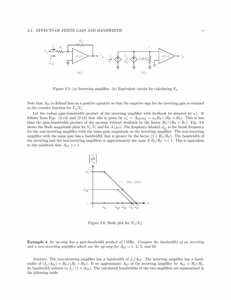
2.1.4 Inverting Amplifier
Figure 2.5(a) shows the circuit diagram of an inverting amplifier. Fig. 2.5(b) shows an equivalent circuitwhich can be used to solve for V−. By inspection, we can write
Vo = −A (s)V− (2.10)
V− =
(ViR1
+VoRF
)(R1‖RF ) (2.11)
These equations can be solved for the voltage-gain transfer function to obtain
VoVi
=− (1/R1)A (s) (R1‖RF )1 + (1/RF )A (s) (R1‖RF )
=−RF/R1
1 + (1 +RF /R1) /A (s)(2.12)
For s = jω and |(1 +RF/R1) /A (jω)| << 1, the voltage-gain transfer function reduces to Vo/Vi −RF/R1.This is the gain which would be predicted if the op-amp is assumed to be ideal.
When Eq. (2.2) is used for A (s), it is straightforward to show that the voltage-gain transfer functionreduces to
VoVi
=−A0f
1 + s/ω0f(2.13)
where A0f is the gain constant with feedback and ω0f is the radian pole frequency with feedback. These aregiven by
A0f =(1/R1)A0 (R1‖RF )
1 + (1/RF )A0 (R1‖RF )=
RF/R11 + (1 +RF/R1) /A0
(2.14)
ω0f = ω0
(1 +A0
R1‖RFRF
)= ω0
(1 +A0
R1R1 +RF
)(2.15)
2.1. EFFECTS OF FINITE GAIN AND BANDWIDTH v
Figure 2.5: (a) Inverting amplifier. (b) Equivalent circuit for calculating Vo.
Note that A0f is defined here as a positive quantity so that the negative sign for the inverting gain is retainedin the transfer function for Vo/Vi.
Let the radian gain-bandwidth product of the inverting amplifier with feedback be denoted by ω′x. Itfollows from Eqs. (2.14) and (2.15) that this is given by ω′x = A0fω0f = ωxRF/ (RF +R1). This is lessthan the gain-bandwidth product of the op-amp without feedback by the factor RF/ (RF +R1). Fig. 2.6shows the Bode magnitude plots for Vo/Vi and for A (jω). The frequency labeled ω′0f is the break frequencyfor the non-inverting amplifier with the same gain magnitude as the inverting amplifier. The non-invertingamplifier with the same gain has a bandwidth that is greater by the factor (1 +R1/RF ). The bandwidth ofthe inverting and the non-inverting amplifiers is approximately the same if R1/RF << 1. This is equivalentto the condition that A0f >> 1.
Figure 2.6: Bode plot for |Vo/Vi|.
Example 4 An op-amp has a gain-bandwidth product of 1MHz. Compare the bandwidths of an invertingand a non-inverting amplifier which use the op-amp for A0f = 1, 2, 5, and 10.
Solution. The non-inverting amplifier has a bandwidth of fx/A0f . The inverting amplifier has a band-width of (fx/A0f ) × RF/ (R1 +RF ). If we approximate A0f of the inverting amplifier by A0f RF/R1,its bandwidth reduces to fx/ (1 +A0f ). The calculated bandwidths of the two amplifiers are summarized inthe following table.

vi CHAPTER 2 CHARACTERISTICS OF PHYSICAL OP-AMPS
A0f Non-Inverting Inverting1 1MHz 500 kHz2 500 kHz 333 kHz5 200 kHz 167 kHz10 100 kHz 91 kHz
For the case of the ideal op-amp, the V− input to the inverting amplifier is a virtual ground so that theinput impedance Zin is resistive and equal to R1. For the op-amp with finite gain and bandwidth, the V−terminal is not a virtual ground so that the input impedance differs from R1. We use the circuit in Fig.2.5(a) to solve for the input impedance as follows:
Zin =ViI1
=Vi
(Vi − V−) /R1=
R11− (V−/Vo) (Vo/Vi)
(2.16)
To put this into the desired form, we let V−/Vo = −1/A (s) and use Eq. (2.12) for Vo/Vi. The equation forZin reduces to
Zin = R1 +RF
1 +A (s)= R1 +
[1
RF+
(RFA0
+RFA0ω0
s
)−1]−1(2.17)
where Eq. (2.2) has been used. It follows from this equation that Zin consists of the resistor R1 in serieswith an impedance that consists of the resistor RF in parallel with the series combination of a resistor R2and an inductor L given by
R2 =RFA0
(2.18)
L =RFA0ω0
(2.19)
The equivalent circuit for Zin is shown in Fig. 2.7(a). If A0 → ∞, it follows that R2 → 0 and L2 → 0so that Zin → R1. The impedance transfer function for Zin is of the form of a high-pass shelving transferfunction given by
Zin (s) = RDC1 + s/ωz1 + s/ωp
(2.20)
where RDC is the dc resistance, ωp is the pole frequency, and ωz is the zero frequency. These are given by
RDC = R1 +RF
1 +A0(2.21)
ωp =R2 +RF
L= ω0 (1 +A0) (2.22)
ωz =R2 +RF‖R1
L= ω0
(1 +
A0R1R1 +RF
)(2.23)
The Bode magnitude plot for Zin is shown in Fig. 2.7(b).
Example 5 At very low frequencies, an op-amp has the frequency independent open-loop gain A (s) = A0 =2× 10⁵. The op-amp is to be used in an inverting amplifier with a gain of −1000. What is the required ratioRF/R1? For the value of RF/R1, how much larger is the input resistance than R1?
Solution. By Eq. (2.12), we have
−1000 = − RF/R11 + (1 +RF /R1) / (2× 10⁵)

2.1. EFFECTS OF FINITE GAIN AND BANDWIDTH vii
Figure 2.7: (a) Equivalent input impedance. (b) Bode plot for |Zin|.
This can be solved for RF/R1 to obtain
RFR1
=2× 10⁵ + 1
(2× 10⁵/1000)− 1= 1005
By Eq. (2.17), the input resistance can be written
Rin = R1
(1 +
RF/R11 +A0
)= R1
(1 +
1005
1 + 2× 10⁵
)= 1.005R1
Example 6 An op-amp has a dc gain A0 = 2×10⁵ and a gain bandwidth product fx = 1MHz. The op-ampis used in the inverting amplifier of Fig. 2.5(a). The circuit element values are R1 = 1kΩ and RF = 100 kΩ.Calculate the dc gain of the amplifier, the upper cutoff frequency, and the value of the elements in theequivalent circuit for the input impedance. In addition, calculate the zero and the pole frequencies in Hz forthe impedance Bode plot of Fig. 2.7(b).
Solution. The dc voltage gain is −A0f . Eq. (2.14) can be used to calculate A0f to obtain
A0f =2× 105 × (1k‖100k) /1k
1 + 2× 105 × (1k‖100k) /100k = 99.95
By Eqs. (2.3) and (2.15), the upper cutoff frequency f0f is given by
fof =ω0f2π
=106
2× 10⁵
(1 + 2× 10⁵
1k‖100k100k
)= 9.91 kHz
The element values in the equivalent circuit of Fig. 2.7(a) for the input impedance are as follows:
R1 = 1 kΩ, RF = 100 kΩ, R2 = 0.5 Ω, and L = 15.9 mH
where Eqs. (2.18) and (2.19) have been used for R2 and L. The pole and zero frequencies in the Bodeimpedance plot are
fp = f0 (1 +A0) =fxA0
(1 +A0) = 1.00 MHz
fz = f0
(1 +A0
R1R1 +RF
)= 9.91 kHz

viii CHAPTER 2 CHARACTERISTICS OF PHYSICAL OP-AMPS
2.2 Effects of Finite Input Resistance
2.2.1 Differential Input Resistance
Because no signal currents flow in the input leads of the ideal op-amp, the input resistance to either leadis infinite. For a physical op-amp, the input resistance is not infinite. To a first approximation, the signalcurrents which flow in the input leads can be modeled by placing a resistor RI between the two leads. Fig.2.8 shows the op-amp symbol with such a resistor added as an external element. The resistor is called thedifferential input resistance. A typical value for RI is 1 MΩ or greater. In the following, we calculate theeffects of RI on the non-inverting and the inverting amplifiers.
Figure 2.8: Op amp with its internal input resistance modeled by an external resistor.
2.2.2 Non-Inverting Amplifier
Figure 2.9(a) shows the circuit diagram of a non-inverting amplifier with the differential input resistancemodeled by an external resistor. Fig. 2.9(b) shows an equivalent circuit which can be used to solve for V−.By inspection, we can write
Vo = A (s) (Vi − V−) (2.24)
V− = VoR1
R1 +RF× RIRI +R1‖RF
+ ViR1‖RF
RI +R1‖RF(2.25)
where A (s) is the op-amp open-loop voltage-gain transfer function. Simultaneous solution of these equationsfor Vo/Vi yields
VoVi
=A′ (s)
1 +A′ (s)R1/ (R1 +RF )=
1 +RF/R11 + (1 +RF /R1) /A′ (s)
(2.26)
where A′ (s) is given by
A′ (s) =RI
RI +R1‖RFA (s) (2.27)
Equation (2.6) gives the voltage-gain transfer function for RI =∞. When this equation is compared toEq. (2.26), it can be concluded that the effect of RI on the voltage gain is to reduce the open-loop transferfunction A (s) by the factor RI/ (RI +R1‖RF ). The effective transfer function is denoted by A′ (s). WhenEq. (2.2) is used for A (s), A′ (s) can be written
A′ (s) =A′0
1 + s/ω0(2.28)
where A′0 is given by
A′0 =RI
RI +R1‖RFA0 (2.29)
We see that the effect of RI is to reduce the dc gain constant of A (s) by the factor RI/ (RI +R1‖RF ).Because the pole frequency is unchanged, it follows that the gain bandwidth product is reduced by thefactor RI/ (RI +R1‖RF ).

2.2. EFFECTS OF FINITE INPUT RESISTANCE ix
Figure 2.9: (a) Non-inverting amplifier. (b) Equivalent circuit for calculating Zin and Vo/Vi.
It follows from Fig. 2.9(b) that the input impedance of the non-inverting amplifier is given by
Zin =ViI1
=Vi(
Vi−VoR1/(R1+RF )RI+R1‖RF
) =RI +R1‖RF
1− (Vo/Vi)R1/ (R1 +RF )(2.30)
When Eq. (2.26) is used for Vo/Vi, this expression reduces to
Zin =
(1 +
R1A (s)
R1 +RF
)RI +R1‖RF (2.31)
Fig. 2.10(a) shows the equivalent circuit for Zin, where Eq. (2.2) is assumed for A (s). The resistor R andthe capacitor C in the figure are given by
R =R1
R1 +RFA0RI (2.32)
C =1
ω0R=
1 +RF/R1A0ω0RI
(2.33)
Figure 2.10: (a) Equivalent circuit for Zin. (b) Bode plot for |Zin|.
At low frequencies where the capacitor is an open circuit, Zin is resistive and equal to RI +R+R1‖RF .At high frequencies where the capacitor is a short circuit, Zin is resistive and equal to RI + R1‖RF . It

x CHAPTER 2 CHARACTERISTICS OF PHYSICAL OP-AMPS
follows that the input impedance function is a low-pass shelving function. The transfer function for Zin canbe written
Zin = (RI +R+R1‖RF )1 + s/ωz1 + s/ω0
(2.34)
where ωz is given by
ωz =
(1 +
R
RI +R1‖RF
)ω0 (2.35)
The Bode magnitude plot for Zin is shown in Fig. 2.10(b). Because |Zin| ≥ RI and RI is usually very large,it follows that Zin can be approximated by an open circuit in most applications.
2.2.3 Inverting Amplifier
Figure 2.11(a) shows the circuit diagram of an inverting amplifier with the differential input resistance ofthe op-amp modeled as an external resistor. Fig. 2.11(b) shows an equivalent circuit which can be used tosolve for V−. By inspection, we can write
Vo = −A (s)V− (2.36)
V− =
(ViR1
+VoRF
)(RI‖R1‖RF ) =
RIRI +R1‖RF
(ViR1
+VoRF
)(R1‖RF ) (2.37)
where A (s) is the op-amp open-loop voltage-gain transfer function. These equations can be solved for thevoltage gain of the circuit to obtain
VoVi
= − (1/R1)A′ (s) (R1‖RF )1 + (1/RF )A′ (s) (R1‖RF )
= − RF/R11 + (1 +RF/R1) /A′ (s)
(2.38)
where A′ (s) is the effective open-loop gain given by Eq. (2.27).
Figure 2.11: (a) Inverting amplifier. (b) Equivalent circuit for calculating Vo/Vi.
Equation (2.12) gives the voltage-gain transfer function for RI = ∞. When this equation is comparedto Eq. (2.38), it can be seen that the effect of RI on the voltage gain is to reduce the open-loop transferfunction A (s) by the factor RI/ (RI +R1‖RF ). This is the same as the effect of RI on the non-invertingamplifier.

2.3. EFFECTS OF NON-ZERO OUTPUT RESISTANCE xi
It follows from Fig. 2.11(a) that the input impedance of the inverting amplifier is given by
Zin =ViI1
=Vi
(Vi − V−) /R1=
R11− (V−/Vo) (Vo/Vi)
(2.39)
To put this in the desired form, we let V−/Vo = −1/A (s) and use Eq. (2.38) for Vo/Vi. The equation forZin reduces to
Zin = R1 +RI‖(
RF1 +A (s)
)
= R1 +RI‖[
1
RF+
(RFA0
+RFA0ω0
s
)−1]−1(2.40)
The analogous circuit for Zin is shown in Fig. 2.12(a), where R2 and L are given by Eqs. (2.18) and (2.19).
Figure 2.12: (a) Equivalent circuit for Zin. (b) Bode plot for |Zin|.
The impedance transfer function for Zin is of the form of a high-pass shelving transfer function given by
Zin (s) = RDC1 + s/ωz1 + s/ωp
(2.41)
where RDC is the dc resistance, ωp is the pole frequency, and ωz is the zero frequency. These are given by
RDC = R1 +RI‖(
RF1 +A0
)(2.42)
ωp =R2 +RI‖RF‖R1
L= ω0
(1 +
A0R1‖RIR1‖RI +RF
)(2.43)
ωz =R2 +RI‖RF
L= ω0
(1 +
A0RIRI +RF
)(2.44)
The Bode magnitude plot for Zin is shown in Fig. 2.12(b).
2.3 Effects of Non-Zero Output Resistance
2.3.1 Open-Loop Output Resistance
The output impedance of the ideal op-amp is zero. For a physical op-amp, the output impedance is not zero.To model it, we place a resistor RO in series with the op-amp output. Fig. 2.13 shows the op-amp symbolwith such a resistor added as an external element. The resistor is called the open-loop output resistance. Atypical value for RO is 100Ω. We use the model in Fig. 2.13 to calculate the effects of RO on the invertingand the non-inverting amplifiers in the following. In the analyses, we assume that the differential inputresistance can be neglected, i.e. replaced by an open circuit.

xii CHAPTER 2 CHARACTERISTICS OF PHYSICAL OP-AMPS
Figure 2.13: Op-amp symbol with the output resistance modeled by an external resistor.
2.3.2 Non-Inverting Amplifier
Figure 2.14 shows the circuit diagram of a non-inverting amplifier with the op-amp output resistance modeledas an external resistor. To solve for the voltage gain of the circuit, we can write by inspection
Vo = A (s) (Vi − V−)RF +R1
RO +RF +R1(2.45)
V− = VoR1
RF +R1(2.46)
where a voltage divider relation is used in the former equation. These equations can be solved for the voltagegain to obtain
VoVi
=A′ (s)
1 +A′ (s)R1/ (R1 +RF )=
1 +RF/R11 + (1 +RF /R1) /A′ (s)
(2.47)
where A′ (s) is given by
A′ (s) = A (s)RF +R1
RO +RF +R1(2.48)
(The A′ (s) here is not the same as that defined in Sec. 2.2.)
Figure 2.14: Non-inverting amplifier.
It can be concluded that the effect of RO is to reduce the effective open-loop voltage-gain transfer functionby the factor (RF +R1) / (RO +RF +R1). When A (s) is modeled by the transfer function in Eq. (2.2), itfollows that the dc gain constant A0 is reduced by the same factor, the pole frequency is not changed, andthe gain-bandwidth product is reduced by the factor (RF +R1) / (RO +RF +R1).
The output impedance of the non-inverting amplifier is given by the ratio of the open-circuit outputvoltage Vo(oc) to the short-circuit output current Io(sc), or equivalently the ratio of Vo(oc)/Vi to Io(sc)/Vi. Eq.(2.47) gives Vo(oc)/Vi. To solve for the short-circuit output current, we connect the Vo node in Fig. 2.14 toground. The current which flows in the ground connection is the short-circuit output current. When the Vonode is grounded, there is no feedback voltage, i.e. V− = 0. It follows that the current which flows in the

2.3. EFFECTS OF NON-ZERO OUTPUT RESISTANCE xiii
ground connection is Io(sc) = A (s)Vi/RO so that Io(sc)/Vi = A (s) /RO. Thus the output impedance of theamplifier is obtained by dividing Eq. (2.47) by A (s) /RO. It is given by
Zout =Vo(oc)Io(sc)
=RO‖ (R1 +RF )
1 +A′ (s)R1/ (R1 +RF )(2.49)
When the transfer function in Eq. (2.2) is used for A (s), the expression for Zout reduces to
Zout = RDC1 + s/ω01 + s/ωp
(2.50)
where RDC and ωp are given by
RDC =RO‖ (R1 +RF )
1 +A0R1/ (RO +RF +R1)(2.51)
ωp =
(1 +A0
R1RO +RF +R1
)ω0 (2.52)
The equivalent circuit for Zout is given in Fig. 2.15(a), where R2 and L are given by
R2 = [RO‖ (RF +R1)]A0R1/ (RO +RF +R1)
1 +A0R1/ (RO +RF +R1)(2.53)
L =R2ωp
(2.54)
Figure 2.15: (a) Equivalent circuit for Zout. (b) Bode plot for |Zout|.
Example 7 At very low frequencies, an op-amp has the frequency independent open-loop gain A (s) = A0 =2 × 10⁵ and an open-loop output resistance RO = 100Ω. The op-amp is to be used in a non-invertingamplifier having a voltage gain of 100. If the amplifier is designed with the assumption that the op-amp isideal, calculate the actual gain of the circuit and its output resistance.
Solution. To obtain a voltage gain of 100 with an ideal op-amp, we require 1+RF/R1 = 100. To satisfythis, we can choose R1 = 100Ω and RF = 9.9 kΩ. The voltage gain is calculated from Eqs. (2.48) and (2.47)as follows:
A′ = 2× 1059.9k+ 100
100 + 9.9k+ 100= 1.98× 10⁵
VoVi
=1.98× 10⁵
1 + 1.98× 105 × 100/ (100 + 9.9k)= 99.95
The output resistance is calculate from Eq. (2.51) to obtain
RDC =100‖ (100 + 9.9k)
1 + 1.98× 105 × 100/ (100 + 9.9k)= 0.05Ω

xiv CHAPTER 2 CHARACTERISTICS OF PHYSICAL OP-AMPS
2.3.3 Inverting Amplifier
Figure 2.16(a) shows the circuit diagram of an inverting amplifier with RO shown as an external resistor.Fig. 2.16(b) shows an equivalent circuit which can be used to calculate V− and Vo. By inspection, we canwrite
V− =
(ViR1
+VoRF
)(R1‖RF ) (2.55)
Vo = −A (s)V−RF
RO +RF+ V−
RORO +RF
(2.56)
where two voltage divider relations are used in the latter equation. These equations can be solved for thevoltage gain to obtain
VoVi
= − (1/R1)A′′ (s) (R1‖RF )
1 + (1/RF )A′′ (s) (R1‖RF )= − RF /R1
1 + (1 +RF/R1) /A′′ (s)(2.57)
where A′′ (s) is given by
A′′ (s) = A (s)RF
RO +RF− RORO +RF
(2.58)
Figure 2.16: (a) Inverting amplifier. (b) Equivalent circuit for calculating Vo/Vi.
Equation (2.12) gives the voltage-gain transfer function for the inverting amplifier for the case RO = 0.When this equation is compared to Eq. (2.57), it can be seen that the effect of RO is to cause the open looptransfer function A (s) to be changed to A′′ (s) given by Eq. (2.58). When Eq. (2.2) is used for A (s), A′′ (s)can be written
A′′ (s) = A′′01− s/ωz1 + s/ω0
(2.59)
where A0 and ωz are given by
A′′0 =RF
RO +RF
(A0 −
RORF
)(2.60)
ωz =
(A0RFRO
− 1
)ω0 (2.61)
2.4. OUTPUT WAVEFORM DISTORTION xv
Thus the effect of RO is to reduce the gain constant from A0 to A′′0 and to introduce a right-half-plane zero
into the transfer function.When Eq. (2.59) is used in Eq. (2.57), it follows that the voltage-gain transfer function for the inverting
amplifier reduces toVoVi
= A0f1− s/ωz1 + s/ω0f
(2.62)
where A0f and ω0f are given by
A0f =A′′0RF/ (R1 +RF )
1 +A′′0R1/ (R1 +RF )=
RF/R11 + (1 +RF/R1) /A′′0
(2.63)
ω0f =1 +A′′0R1/ (R1 +RF )
1− (ω0/ω1)R1/ (R1 +RF )ω0 (2.64)
The output impedance of the inverting amplifier is the same as that for the non-inverting amplifier givenby Eq. (2.50). This follows because the circuit seen looking into the output terminal with the source zeroedis the same for both configurations.
2.4 Output Waveform Distortion
2.4.1 Types of Distortion
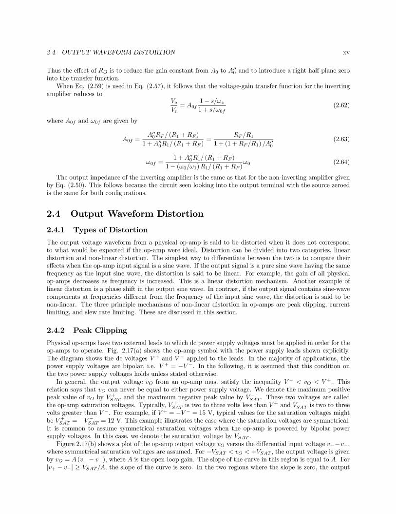
The output voltage waveform from a physical op-amp is said to be distorted when it does not correspondto what would be expected if the op-amp were ideal. Distortion can be divided into two categories, lineardistortion and non-linear distortion. The simplest way to differentiate between the two is to compare theireffects when the op-amp input signal is a sine wave. If the output signal is a pure sine wave having the samefrequency as the input sine wave, the distortion is said to be linear. For example, the gain of all physicalop-amps decreases as frequency is increased. This is a linear distortion mechanism. Another example oflinear distortion is a phase shift in the output sine wave. In contrast, if the output signal contains sine-wavecomponents at frequencies different from the frequency of the input sine wave, the distortion is said to benon-linear. The three principle mechanisms of non-linear distortion in op-amps are peak clipping, currentlimiting, and slew rate limiting. These are discussed in this section.
2.4.2 Peak Clipping
Physical op-amps have two external leads to which dc power supply voltages must be applied in order for theop-amps to operate. Fig. 2.17(a) shows the op-amp symbol with the power supply leads shown explicitly.The diagram shows the dc voltages V + and V − applied to the leads. In the majority of applications, thepower supply voltages are bipolar, i.e. V + = −V −. In the following, it is assumed that this condition onthe two power supply voltages holds unless stated otherwise.
In general, the output voltage vO from an op-amp must satisfy the inequality V − < vO < V +. Thisrelation says that vO can never be equal to either power supply voltage. We denote the maximum positivepeak value of vO by V +SAT and the maximum negative peak value by V −SAT . These two voltages are calledthe op-amp saturation voltages. Typically, V +SAT is two to three volts less than V
+ and V −SAT is two to threevolts greater than V −. For example, if V + = −V − = 15 V, typical values for the saturation voltages mightbe V +SAT = −V −SAT = 12 V. This example illustrates the case where the saturation voltages are symmetrical.It is common to assume symmetrical saturation voltages when the op-amp is powered by bipolar powersupply voltages. In this case, we denote the saturation voltage by VSAT .
Figure 2.17(b) shows a plot of the op-amp output voltage vO versus the differential input voltage v+−v−,where symmetrical saturation voltages are assumed. For −VSAT < vO < +VSAT , the output voltage is givenby vO = A (v+ − v−), where A is the open-loop gain. The slope of the curve in this region is equal to A. For|v+ − v−| ≥ VSAT/A, the slope of the curve is zero. In the two regions where the slope is zero, the output

xvi CHAPTER 2 CHARACTERISTICS OF PHYSICAL OP-AMPS
Figure 2.17: (a) Op amp with power supply connections shown. (b) vO versus v+−v−. (c) Output waveforms.
voltage does not change when the input voltage is changed. Fig. 2.17(c) shows the effect of clipping on asine wave output signal. For the larger amplitude waveform, it can be seen that the maximum value of |vO|is limited to VSAT . The output is said to be peak clipped at this value. The smaller amplitude waveform isnot clipped.
Peak clipping is a non-linear distortion mechanism. For a sine-wave input signal, a Fourier series analysiscan be used to show that a peak clipped output signal contains frequency components that are not at thefrequency of the input signal. If the clipping voltages are symmetrical, it can be shown that the distortioncomponents in the output signal are at odd harmonics of the input signal. For example, a 1 kHz inputsignal would generate a 1 kHz output signal plus distortion components at 3 kHz, 5 kHz, 7 kHz, etc. Whenthe clipping voltages are not symmetrical, it can be shown that both even and odd order harmonics aregenerated by the clipping. We have illustrated peak clipping here for an op-amp with no feedback. Iffeedback is added, the peak clipping voltages are not changed. Thus the graph of the output voltage versusinput voltage is the same as that shown in Fig. 2.17(b) except that the slope of the curve in the centerregion is reduced by the feedback. To prevent peak clipping from occurring, either the peak value of theinput signal or the gain of the op-amp must be reduced.
2.4.3 Current Limiting
All physical op-amps have internal current limiting circuits which limit the maximum output current toprevent failure of the internal transistors that supply the current. Fig. 2.18(a) shows an op-amp with a loadresistor connected to its output. The output current is given by iO = vO/RL. For a given output voltage,the output current varies inversely with the load resistance. If the resistance is decreased, the output currentwill increase until the internal protection circuits are activated to limit the current. When this occurs, theop-amp exhibits peak clipping at its output. Current limiting causes the op-amp to clip at an output voltage

2.4. OUTPUT WAVEFORM DISTORTION xvii
that is less than its saturation voltage.
Figure 2.18: (a) Op amp with a load resistor. (b) Plots of vO versus v+ − v− showing effects of currentlimiting.
Let the maximum value of the op-amp output current be denoted by IM . For a given load resistance RL,the magnitude of the peak output voltage is limited to IMRL. If RL > VSAT /IM , the op-amp clips beforecurrent limiting occurs. If RL < VSAT /IM , the op-amp exhibits current limiting before clipping occurs.Fig. 2.18(b) shows the graph of the op-amp output voltage versus differential input voltage for three cases.One case corresponds to no load resistor so that the graph is identical to that shown in Fig. 2.17(b). Theother cases illustrate the effects of current limiting for two values of load resistance. The graph assumes thatRL1 > RL2.
Example 8 An op-amp has the saturation voltages V +SAT = V + − 2.5 V and V −SAT = V − + 2.5 V. Thecurrent limited output current is IM = 25 mA. The op-amp is powered by bipolar supply voltages of +15 Vand −15 V. Determine the lowest load resistance that can be driven without current limiting. Determine thepeak output voltage for a load resistance of 100Ω.
Solution. The magnitude of the peak output voltage is 15− 2.5 = 12.5 V. For a current limit of 25 mA,the minimum load resistance that can be driven to a peak voltage of 12.5 V is RL(min) = 12.5/0.025 = 500Ω.For RL = 100Ω, the magnitude of the peak output voltage is 100× 0.025 = 2.5 V.
Example 9 Figure 2.19(a) shows a non-inverting amplifier with a capacitive load. The input signal to theamplifier is a square wave. The magnitude of the output current is limited to the value IM . Determine thewaveform of the amplifier output voltage.
Solution. A voltage step applied to a capacitor causes an impulse of current to flow. Because the op-ampis current limited, it cannot supply an impulse of current to the load capacitor. Each time the input squarewave switches states, the op-amp is driven into current limiting. For an output current iO = ±IMAX , thecapacitor voltage has a time derivative given by dvO/dt = ±IM/CL, where we assume that the current inRF can be neglected. Thus current limiting has the effect of limiting the maximum time derivative of vOwith the capacitive load. Fig. 2.19(b) shows plot of the output voltage waveform, where it is assumed thatthe frequency of the square wave is low enough so that the output voltage reaches its final peak value eachhalf cycle of the signal. The dotted lines in the figure represent the waveform for the case of no currentlimiting.
2.4.4 Slew Rate Limiting
An op-amp amplifier is said to be unstable if it puts out an ac signal with no input signal. To preventinstability problems, the internal circuits of most op-amps contain a capacitor that is called the compensation

xviii CHAPTER 2 CHARACTERISTICS OF PHYSICAL OP-AMPS
Figure 2.19: (a) Non-inverting amplifier with capacitive load. (b) Square wave response showing the effectsof current limiting.
capacitor. The op-amp output voltage is proportional to the voltage across this capacitor. The circuits whichcharge and discharge the capacitor are current limited. As is illustrated by Example 9, the time derivativeof the voltage across a capacitor is limited by the current available to charge it. Thus the compensationcapacitor and the current available to charge it set the maximum time derivative of the op-amp outputvoltage. This maximum time derivative is called the op-amp slew rate.
The basic units of slew rate are volts per second (V/s). In op-amp specifications, it is usually specifiedin volts per microsecond (V/µs). The slew rate is related to the compensation capacitor and the maximumcurrent available to charge it by the equation
SR =I1Cc
(2.65)
where Cc is the capacitor and I1 is the peak value of the charging current. A typical general purpose op-ampmight have a compensation capacitor with a value of 30 pF and a slew rate of 1 V/µs. Eq. (2.65) can be usedto calculate I1 = 106× 30p = 30 µA. This calculation illustrates how small the internal currents in op-ampscan be. Most op-amps have symmetrical slew rates. That is the slew rate is the same for an increasing ora decreasing output voltage. The slew rates are not symmetrical if the peak positive current available tocharge the compensation capacitor is not the same as the peak negative current.
If an op-amp does not exhibit slewing, the time derivative of the output voltage is proportional to thetime derivative of the input voltage. This is not true when the op-amp slews. Fig. 2.20(a) illustrates theeffect of slewing on the sine-wave response of an op-amp. The figure shows the waveforms of the outputvoltage when the op-amp is slewing and when it is not slewing. The waveform with slewing is a trianglewave having a peak voltage obtained by multiplying the slew rate by one-fourth the period. It is given by
VP = SR× T4=
I14fCc
(2.66)
where the period T is related to the frequency f by T = 1/f . It can be seen from this expression that thepeak output voltage is not a function of the amplitude the input voltage. Thus the output voltage does notincrease if the input voltage is increased. This means that slewing is a non-linear phenomenon.
The non-linear distortion generated when an op-amp slews is referred to as slewing induced distortion.With a sine wave input signal, a Fourier series analysis can be used to show that the distortion componentsin the output signal are at odd harmonics of the signal frequency. This assumes symmetrical slew rates. Ifthe op-amp slew rates are not symmetrical, both even and odd harmonics are generated.
If an op-amp does not slew, the maximum peak output voltage is VSAT . For a sine-wave input signal,the corresponding output voltage is given by
vO (t) = VSAT sin (2πft) (2.67)

2.4. OUTPUT WAVEFORM DISTORTION xix
Figure 2.20: (a) Sine-wave output without slewing and with full slewing. (b) Peak sine-wave output voltageversus frequency.
The time derivative of this expression is
d
dtvO (t) = 2πfVSAT cos (2πft) (2.68)
The maximum value of the magnitude of the derivative is 2πfVSAT . This must be less than the slew rate ofthe op-amp if it is not to exhibit slewing. The frequency above which slewing occurs is given by
f1 =SR
2πVSAT(2.69)
For f < f1, the peak output voltage is limited by clipping. For f ≥ f1, the peak output voltage is limitedby slewing. The maximum undistorted peak sine-wave output voltage is given by
VP = VSAT for f ≤ f1=
SR
2πffor f > f1 (2.70)
Figure 2.20(b) shows a plot of VP as a function of frequency. Because the voltage decreases with increasingfrequency for f ≥ f1, f1 is called the large-signal bandwidth of the op-amp.
Example 10 The op-amp of Example 8 has a slew rate of 1 V/µs. Calculate the large-signal bandwidth ofthe op-amp. Calculate the peak value of the largest amplitude sine-wave that the op-amp can put out at afrequency of 20 kHz.
Solution. By Eq. (2.69), the large signal bandwidth is f1 = 106/ (2π × 12.5) = 12.7 kHz. By Eq. (2.70),the peak value of the largest amplitude output sine wave is VP = 106/ (2π × 20k) = 7.96 V.
xx CHAPTER 2 CHARACTERISTICS OF PHYSICAL OP-AMPS
2.5 DC Offsets
2.5.1 Offset Voltage
Although integrated-circuit op-amps are fabricated with precision, it is impossible to achieve circuits whichhave a zero dc output voltage when both input voltages are zero. The output offset voltage of a physicalop-amp is the dc voltage that is present at its output when both of its inputs are grounded. The expressionfor the op-amp output voltage when an offset voltage is present is written
vO = A (v+ − v− + VOS) (2.71)
With v+ = v− = 0, the dc offset voltage at the output is AVOS . The voltage VOS is defined as the inputoffset voltage. It is equivalent to the dc voltage at the input of an ideal op-amp that produces the same dcoffset voltage at its output. A typical value for VOS is 5 mV or less.
It can be seen from Eq. (2.71) that vO = 0 if v− − v+ = VOS. Thus an alternate definition of the inputoffset voltage is the differential dc voltage which must be applied across the op-amp inputs in order to achievea zero dc output voltage, where the positive reference node is the v− input. In op-amp specifications, VOS iscommonly specified without regard to its algebraic sign. The specified value represents the maximum valueof the magnitude of the offset voltage for that particular op-amp.
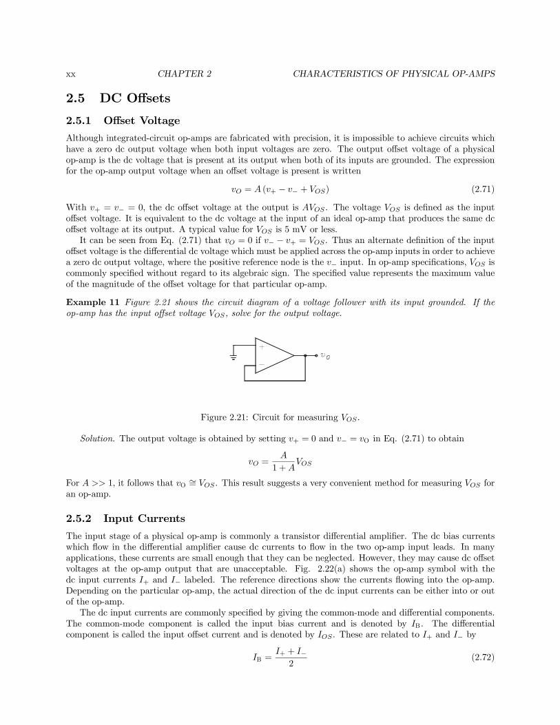
Example 11 Figure 2.21 shows the circuit diagram of a voltage follower with its input grounded. If theop-amp has the input offset voltage VOS, solve for the output voltage.
Figure 2.21: Circuit for measuring VOS.
Solution. The output voltage is obtained by setting v+ = 0 and v− = vO in Eq. (2.71) to obtain
vO =A
1 +AVOS
For A >> 1, it follows that vO ∼= VOS. This result suggests a very convenient method for measuring VOS foran op-amp.
2.5.2 Input Currents
The input stage of a physical op-amp is commonly a transistor differential amplifier. The dc bias currentswhich flow in the differential amplifier cause dc currents to flow in the two op-amp input leads. In manyapplications, these currents are small enough that they can be neglected. However, they may cause dc offsetvoltages at the op-amp output that are unacceptable. Fig. 2.22(a) shows the op-amp symbol with thedc input currents I+ and I− labeled. The reference directions show the currents flowing into the op-amp.Depending on the particular op-amp, the actual direction of the dc input currents can be either into or outof the op-amp.
The dc input currents are commonly specified by giving the common-mode and differential components.The common-mode component is called the input bias current and is denoted by IB . The differentialcomponent is called the input offset current and is denoted by IOS. These are related to I+ and I− by
IB =I+ + I−
2(2.72)

2.5. DC OFFSETS xxi
IOS = I+ − I− (2.73)
If I+ = I−, we note that IB = I+ = I− and IOS = 0. Typical values are 100 nA or less for IB and 20 nAor less for IOS. In op-amp specifications, IB and IOS are commonly specified without regard to algebraicsign. The specified values represents the maximum value of the magnitude of the currents for that particularop-amp. Fig. 2.22(b) shows an equivalent circuit of the op-amp with the input currents represented byexternal common-mode and differential current sources.
Figure 2.22: (a) Op amp with input currents labeled. (b) Equivalent circuit for input currents.
Example 12 Figure 2.23(a) shows an inverting op-amp amplifier with a resistor connected in series withits non-inverting input. The op-amp has the input bias current IB . Solve for the output voltage vO. Assumethat A→∞, IOS = 0, and VOS = 0.
Solution. Because IOS = 0, the dc input currents are I+ = I− = IB . Fig. 2.23(b) shows the equivalentcircuit which can be used to calculate V+ and V−. These are given by
V+ = −IBR2
V− =
(VIR1
+VORF
− IB)(R1‖RF )
Because A→∞, the output voltage can be solved for by setting V+ = V− to obtain
VO = −RFR1
[VI +
(1 +
R1RF
)(R2 −R1‖RF ) IB
]
It can be seen from this equation that the dc offset at the output caused by IB is zero if R2 = R1‖RF .This is equivalent to the condition that the resistance seen looking out of the V+ and V− inputs be equalwith VI and VO zeroed.
Example 13 Figure 2.24 shows the circuit diagram of a non-inverting amplifier with a resistor connected inseries with its input. The op-amp has the input bias current IIB. Solve for the output voltage VO . Assumethat A→∞, IOS = 0, and VOS = 0.
Solution. Figure 2.24(b) shows an equivalent circuit for calculating V+ and V−. By inspection, these aregiven by
V+ = VI − IBR2
V− = VOR1
R1 +RF− IB (R1‖RF )

xxii CHAPTER 2 CHARACTERISTICS OF PHYSICAL OP-AMPS
Figure 2.23: (a) Inverting amplifier. (b) Equivalent circuit for calculating v+ and v−.
Figure 2.24: (a) Non-inverting amplifier. (b) Equivalent circuit for calculating v+ and v−.

2.6. MISCELLANEOUS SPECIFICATIONS xxiii
The output voltage can be solved for by setting v+ = v− to obtain
VO =
(1 +
RFR1
)[VI + (R1‖RF −R2) IB ]
It can be seen from this equation that the dc offset at the output caused by IB is zero if R2 = R1‖RF . Thisis the same condition as for the inverting amplifier of Example 12.
2.5.3 Condition for Zero Offset Due to IB
Examples 12 and 13 show that the condition for zero offset voltage at the op-amp output due to IB arethe same for the inverting amplifier and the non-inverting amplifier. The condition is that the resistanceseen looking out of the v+ and v− inputs be equal, where the two resistances are calculated with vI and vOzeroed. Without resistor R2 in the circuits, the condition cannot be met. In circuits containing capacitors,each capacitor must be replaced with an open-circuit when calculating the resistance seen looking out of thev+ and v− inputs.
2.6 Miscellaneous Specifications
This section covers several specifications on physical op-amps that have not been covered in the precedingsections.
2.6.1 Common-Mode Rejection Ratio
The output voltage from an ideal op-amp is a function only of the difference or differential voltage across itstwo inputs. In contrast, physical op-amps have an output voltage that can be written
Vo = A (s) (V+ − V−) +A (s)
ρ× V+ + V−
2(2.74)
where A (s) is the differential voltage gain and A (s) /ρ is the common-mode voltage gain. The constant ρ isthe op-amp common-mode rejection ratio. It represents the ratio of the differential gain to the common-modegain. It is commonly expressed in dB by the equation 20 log ρ. A typical value for ρ is 105 (100 dB). In mostapplications, the common-mode rejection ratio is large enough so that the common-mode term in Eq. (2.74)can be neglected.
2.6.2 Input Common-Mode Range
In some applications of op-amps, the external circuits cause a common-mode voltage, e.g. a dc voltage, to bepresent at both inputs. If this common-mode voltage is out of range, the differential amplifier input stage tothe op-amp can cease to operate. The input common-mode range is the range on the common-mode inputvoltage over which the differential amplifier remains linear. For example, with the bipolar power supplyvoltages V + = −V − = 15 V, the input common-mode range might be from −10 V to +10 V. A dc common-mode voltage applied to the two op-amp input terminals that is outside this range can cause the op-amp tocease to operate.
2.6.3 Input Differential Range
The input differential range is the maximum difference voltage that can be safely applied between the twoop-amp inputs. When an op-amp is operated with negative feedback, the difference voltage between theinputs is very small. (It is zero for the ideal op-amp.) However, if the op-amp clips, current limits, or slews,it loses feedback and the differential input voltage can become large. Another example of a case where thedifferential input voltage might be large is when the op-amp is used as a comparator.

xxiv CHAPTER 2 CHARACTERISTICS OF PHYSICAL OP-AMPS
2.6.4 Power Supply Rejection Ratio
When either power supply voltage changes, the output offset voltage of a physical op-amp can change. Thischange in output offset voltage can be converted to a change in the input offset voltage by dividing by theopen-loop gain of the op-amp. The power supply rejection ratio (PSRR) is defined as the ratio of the changein input offset voltage to the change in the power supply voltage, where one power supply voltage is variedand the other is held constant. In general, a different value is obtained when each power supply voltage ischanged. A typical maximum value is 20 µV/V.
2.7 Linear Op-Amp Macromodels
2.7.1 Macromodels
A macromodel is a circuit model which is simpler than the original circuit but retains an accurate represen-tation of the performance of that circuit. In this section, we develop a linear macromodel of the op-amp.The macromodel can be used with computer simulation programs such as SPICE to predict the voltagegain, input impedance, and output impedance of op-amp circuits. More accurate macromodels which modelnon-linear effects such as clipping, current limiting, and slewing require the addition of diodes and transistorsto the model.
2.7.2 Modeling Input and Output Resistance
Figure 2.1(b) gives the simplest controlled-source model of the op-amp. The input resistance between thev+ and the v− terminals is infinite. The output resistance seen looking into the vO node is zero. We canmodel the differential input resistance by adding a resistor RI between the v+ and the v− nodes. In addition,we can model the open-loop output resistance by adding a resistor RO in series with the output lead. Themodified circuit is shown in Fig. 2.25. The next step in developing the macromodel circuit is to model thefinite bandwidth of the op-amp.
Figure 2.25: Simple macromodel with input and output resistances added.
2.7.3 Modeling the Open-Loop Transfer Function
The input stage of a typical op-amp operates as a voltage controlled current source with a load impedancethat consists of a parallel RC circuit. The current source is controlled by the differential voltage betweenthe op-amp input terminals. Such a circuit is shown in Fig. 2.26(a). The transconductance of the controlledsource in this figure is denoted by gm1. The voltage V1 is given by
V1 = −gm1 (V+ − V−)(R1‖
1
C1s
)= − gm1R1
1 +R1C1s(V+ − V−) (2.75)
The second stage of the typical op-amp operates as a voltage-controlled voltage source having the inputvoltage V1 and an open-circuit output voltage equal to the op-amp open-circuit output voltage. Such acircuit is shown in Fig. 2.26(b). The voltage gain of the controlled source is denoted by −AV , where AV is

2.7. LINEAR OP-AMP MACROMODELS xxv
a positive constant. The output resistance of the source is RO. The open-circuit output voltage is given byVo(oc) = −AV V1.
The op-amp macromodel consists of the two circuits of Fig. 2.26 in combination. Let the open-circuitvoltage gain of this circuit be denoted by A (s). It is given by
A (s) =Vo(oc)V+ − V−
=gm1R1AV1 +R1C1s
(2.76)
This is a single-pole low-pass transfer function having a dc gain constant A0 and a radian pole frequency ω0given by
A0 = gm1R1AV (2.77)
ω0 =1
R1C1(2.78)
Figure 2.26: (a) Input stage model. (b) Gain stage model.
Figure 2.27 shows a modification to the circuit of Fig. 2.26 which makes the circuit more closely agreewith the internal architecture of physical op-amps. The capacitor C1 from the V1 node to ground in theoriginal circuit is replaced by the capacitor Cc from the V1 node to the top of the voltage-controlled voltagesource. By the Miller theorem, the load capacitance on the voltage-controlled current source input stage isthe same if C1 and Cc satisfy the relation
C1 = (1 +AV )Cc (2.79)
Figure 2.27: Modified macromodel circuit.
2.7.4 Completed Model
The circuit of Fig. 2.27 is a better model of physical op-amps if the output resistor RO is broken into twoparts RO1 and RO2 as shown in Fig. 2.28, where RO = RO1+RO2. This circuit more accurately models theoutput impedance of a physical op-amp. In addition, it better models the variation in the op-amp gain withload impedance. This is the completed linear macromodel of the op-amp. A modification to this circuit thatis often used in computer simulations is to make a Norton equivalent circuit of the resistor RO2 in serieswith the voltage source AV V1. The circuit is shown in Fig. 2.29, where gm2 = AV /RO2.

xxvi CHAPTER 2 CHARACTERISTICS OF PHYSICAL OP-AMPS
Figure 2.28: Further modification to the macromodel.
Figure 2.29: Final macromodel circuit.
Example 14 Solve for the open-circuit voltage-gain transfer function of the op-amp macromodel in Fig.2.29. Compare it to the transfer function of Eq. (2.76).
Solution. It follows from Fig. 2.29 that
V1 = [−gm1 (V+ − V−) + V2Ccs](R1‖
1
Ccs
)
Vo(oc) = V2 = [−gm2V1 + V1Ccs](RO2‖
1
Ccs
)
These equations can be solved for the voltage gain of the circuit to obtain
Vo(oc)V+ − V−
= gm1R1gm2RO21− (Cc/gm2) s
1 + [R1 (1 + gm2RO2) +RO2]Ccs
The above equation is of the form of a dc gain constant multiplied by a low-pass shelving transfer function,where the zero in the transfer function is in the right-half complex plane. In contrast, the transfer functionof Eq. (2.76) is of the form of a dc gain constant multiplied by a low-pass transfer function.
Example 15 Solve for the output impedance transfer function for the op-amp macromodel in Fig. 2.29.Form the equivalent circuit which has this impedance transfer function.
Solution. To solve for the output impedance, we zero the differential input voltage and drive the outputnode with a test current source It. The circuit is shown in Fig. 2.30. For this circuit, we can write
Vo = ItRO1 + V2
V2 = (It − gm2V1)×RO2‖(RO1 +
1
Ccs
)
V1 = V2RO1
RO1 + 1/Ccs

2.7. LINEAR OP-AMP MACROMODELS xxvii
Figure 2.30: Circuit for solving for Zout.
These equations can be solved for the output impedance to obtain
Zout =VoIt
= RO1 +RO21 +R1Ccs
1 + [R1 (1 + gm2RO2) +RO2]Ccs
The above equation is of the form of a resistance (RO1) plus a resistance (RO2) multiplied by a low-passshelving transfer function. At low frequencies, the impedance has the value Zout = RO1 + RO2. At highfrequencies, it has the value Zout = RO1 +RO2R1/ [R1 (1 + gm2RO2) +RO2]. The equivalent circuit whichhas this same impedance is given in Fig. 2.31. The elements R and C in this circuit are given by
R =R1
1 + gm2R1
C = Cc (1 + gm2R1)
Figure 2.31: Equivalent circuit for Zout.
Example 16 The macromodel circuit of Fig. 2.29 can be used to model the 741 op-amp with the followingelement values: RI = 2 MΩ, gm1 = 1.38× 10⁻⁴ S, R1 = 100 kΩ, Cc = 20 pF, gm2 = 106S, RO1 = 150Ω,and RO2 = 150Ω. Calculate the dc gain A0, the pole frequency f0, the gain-bandwidth product fx, and thezero frequency fz in the voltage-gain transfer function for the 741 macromodel. Calculate the element valuesfor R and C in the equivalent circuit for the output impedance in Fig. 2.31.
Solution. It follows from Example 14 that the dc gain A0, the pole frequency f0, the gain bandwidthproduct fx, and the zero frequency fz for the 741 macromodel are given by
A0 = gm1R1gm2RO2 = 2.2× 10⁵
f0 =1
2π [R1 (1 + gm2RO2) +RO2]Cc = 5Hz
fx = A0f0 = 1.1MHz

xxviii CHAPTER 2 CHARACTERISTICS OF PHYSICAL OP-AMPS
fz =gm22πCc
= 8.4× 10⁵MHz
Because the zero frequency fz is so much higher than the gain-bandwidth product fx, the zero term inthe transfer function can be neglected for all practical purposes. The values for the elements R and C in theoutput impedance equivalent circuit are R = 9.43 mΩ and C = 212 µF.
2.7.5 Example SPICE Macromodel Subcircuits
The 741 and the LF351 are two general purpose integrated-circuit op-amps that are commonly used in analogdesign. The 741 is a bipolar op-amp, i.e. it is fabricated entirely with bipolar-junction transistors (BJTs).The LF351 is a bi-fet op-amp. It is fabricated with junction field-effect transistors (JFETs) in the inputdiff-amp stage and BJT’s in the following stages. The macromodels for these op-amps can be simulatedin SPICE with subcircuits. A subcircuit in SPICE is a group of statements that is referenced as a singleentity. It is defined by a block of statements starting with a .SUBCKT statement and ending with a .ENDSstatement. In between are one or more statements. Once a subcircuit is defined, it can be called as a devicehaving a name that starts with an “X”. The codes for the 741 and LF351 subcircuits are given below. TheSPICE node numbers for each code are labeled in Fig. 2.29.
*741 OP-AMP SUBCIRCUIT *LF351 OP-AMP SUBCIRCUIT
SUBCKT 741 1 2 3 SUBCKT LF351 1 2 3
RI 1 2 2E6 RI 1 2 2E12
GM1 4 0 1 2 1.38E-4 GM1 4 0 1 2 2.83E-4
R1 4 0 1E5 R1 4 0 1E5
CC 4 5 20E-12 CC 4 5 15E-12
GM2 5 0 4 0 106 GM2 5 0 4 0 283
R01 3 5 150 R01 3 5 50
R02 5 0 150 R02 5 0 25
.ENDS 741 .ENDS LF351