chapter 1 introduction - virginia tech · 2019-02-04 · incremental input resistance within the...
TRANSCRIPT

Stability Analysis of Three-phase AC Power Systems
Based on Measured D-Q Frame Impedances
Bo Wen
Dissertation submitted to the faculty of the Virginia Polytechnic Institute and State University in
partial fulfillment of the requirements for the degree of
Doctor of Philosophy
In
Electrical Engineering
Dushan Boroyevich Chair
Rolando Burgos Co-Chair
Paolo Mattavelli
Daniel J Stilwell
Christopher John Roy
Nov. 18, 2014
Blacksburg, Virginia
Keywords: Distributed power system, impedance, inverters, negative resistance circuits, Nyquist
stability, rectifiers, power system stability, stability, synchronization

Stability Analysis of Three-phase AC Power System
Based on Measured D-Q Frame Impedances
Bo Wen
ABSTRACT
Small-signal stability is of great concern for distributed power systems with a large number of
regulated power converters. These converters are constant-power loads (CPLs) exhibit a negative
incremental input resistance within the output voltage regulation bandwidth. In the case of dc
systems, design requirements for impedances that guarantee stability have been previously
developed and are used in the design and specification of these systems. In terms of three-phase
ac systems, a mathematical framework based on the generalized Nyquist stability criterion
(GNC), reference frame theory, and multivariable control is set forth for stability assessment.
However, this approach relies on the actual measurement of these impedances, which up to now
has severely hindered its applicability. Addressing this shortcoming, this research investigates
the small-signal stability of three-phase ac systems using measured d-q frame impedances. Prior
to this research, negative incremental resistance is only found in CPLs as a results of output
voltage regulation. In this research, negative incremental resistance is discovered in grid-tied
inverters as a consequence of grid synchronization and current injection, where the bandwidth of
the phase-locked loop determines the frequency range of the negative incremental resistance
behavior, and the power rating of inverter determines the magnitude of the resistance. Prior to
this research, grid synchronization stability issue and sub-synchronous oscillations between grid-
tied inverter and its nearby rectifier under weak grid condition are reported and analyzed using
characteristic equation of the system. This research proposes a more design oriented analysis
approach based on the negative incremental resistance concept of grid-tied inverters. Grid
synchronization stability issues are well explained under the framework of GNC. Although
stability and its margin of ac system can be addressed using source and load impedances in d-q
frame, method to specify the shape of load impedances to assure system stability is not reported.
This research finds out that under unity power factor condition, three-phase ac system is
decoupled. It can be simplified to two dc systems. Load impedances can be then specified to
guarantee system stability and less conservative design.

iii
To Prof. Dr. Jinjun Liu
To China Scholarship Council

iv
ACKNOWLEDGEMENTS
First of all, I want to thank Dr. Dushan Boroyevich for giving me the opportunity to do my
M.S. thesis and Ph.D. dissertation at the Center for Power Electronics Systems (CPES) at
Virginia Tech and the numerous valuable ideas and advices he provided to me. During my work,
I have learned a lot in the field of power electronics. He showed me how to conduct high quality
research. In addition, I want to thank him for the understanding and trust during my hard time.
I also want to thank Dr. Rolando Burgos and Dr. Paolo Mattavelli for their guidance on my
research and papers. Every discussion with them has always sparked unforeseen and fruitful
directions in the research.
I want to thank Dr. Christopher John Roy and Dr. Daniel J Stilwell for kindly accepting the
invitation to be my Ph.D. advisory committee and their interest in this work.
I want to thank Dr. Zhiyu Shen, Dr. Marko Jaksic, Dr. Gerald Francis, Mr Igor Cvetkovic, Dr.
Dong Dong, Mr Bo Zhou, Dr. Xuning Zhang, Dr. Ruixi Wang, Dr. Rixin Lai, Dr. Dong Jiang,
Dr. Di Zhang for helping me to grow up in laboratory.
I would like to acknowledge the work of the CPES staff, Ms Marianne Hawthorne, Ms Teresa
Shaw, Mr David Gilham, Ms Teresa Rose, Ms Linda Long, Dr. Wenli Zhang.
Many thanks to my friends: Dr. Yipeng Su, Dr. Weiyi Feng, Dr. Xiao Cao, Mr Feng Yu, Mr
Shuilin Tian, Dr. Daocheng Huang, Dr. Zhenyu Zhang, Dr. Bin Xue, Dr. Xinhao Ye, Mr
Xiucheng Huang, Mr Zhengyang Liu, Mr Yucheng Yang, Mr Yang Jiao, Mr Lingxiao Xue, Mr
Chao Fei, Ms Virginia Li and many others. They made the life in Blacksburg more enjoyable.
I want to express my sincere gratitude to my parents and sister for their worry and support to
my life in the US.

v
TABLE OF CONTENTS
Chapter 1 Introduction ............................................................................................................... 1
1.1 Background .......................................................................................................................... 1
1.1.1 Impedance-based dc system stability analysis .............................................................. 3
1.1.2 Impedance-based ac system stability analysis .............................................................. 7
1.2 Motivation and Objective ................................................................................................... 10
1.3 Disseration Outline and Summary of Contributions .......................................................... 12
Chapter 2 Modeling of Voltage Source Converters ................................................................. 14
2.1 Small-signal Models of VSCs ............................................................................................ 15
2.2 Design of feedback control system for VSCs .................................................................... 21
2.3 Input and output impedance of VSCs ................................................................................ 39
2.3.1 Open loop output impedances of VSI ......................................................................... 41
2.3.2 VSI Impedance with current feedback control ........................................................... 44
2.3.3 VSI Impedance with current and voltage feedback control ........................................ 46
2.3.4 AFE input impedances ................................................................................................ 49
2.4 D-Q Frame Impedance Measurement ................................................................................ 51
2.4.1 Algorithm .................................................................................................................... 52
2.4.2 Measurement Setup ..................................................................................................... 54
2.4.3 Experimental Results .................................................................................................. 55
2.5 Phase-Locked Loop ............................................................................................................ 57
Chapter 3 Small-signal Stability in the Presence of Constant Power Load ............................. 61
3.1 Introduction ........................................................................................................................ 61
3.2 System Setup and Parameters ............................................................................................ 62
vi
3.3 Description Of Experimental Tests Conducted.................................................................. 64
3.4 Experimental Results ......................................................................................................... 67
3.5 Discussion .......................................................................................................................... 74
Chapter 4 Modeling of Voltage Source Converters Including Phase-locked Loop ................. 77
4.1 Introduction ........................................................................................................................ 77
4.2 Power Stage Small-Signal Model ...................................................................................... 79
4.3 Influence of PLL ................................................................................................................ 81
4.4 Impedance with Current Control and PLL ......................................................................... 86
4.5 Influence of Power Flow Control Loop ............................................................................. 92
4.6 Influence of PLL on Input Impedance of AFE .................................................................. 96
4.7 Stability Analysis using the Proposed Model .................................................................... 99
4.7.1 Grid-tied inverter system ............................................................................................ 99
4.8 Experimental Verification ................................................................................................ 107
4.8.1 Grid-tied inverter system .......................................................................................... 107
4.8.2 AFE ........................................................................................................................... 117
Chapter 5 Synchronization Stability Issues Caused by PLL Dynamics ................................ 121
5.1 Introduction ...................................................................................................................... 121
5.2 Synchronization Instability between Parallele-Connected Three-Phase VSCs ............... 123
5.2.1 Components in the system and their parameters ....................................................... 123
5.2.2 Synchronization instability ....................................................................................... 127
5.3 PLL-Based Stability Analysis .......................................................................................... 129
5.4 Impedance-Based Analysis .............................................................................................. 131
5.4.1 Impedance of each components ................................................................................ 136

vii
5.4.2 Stability analysis ....................................................................................................... 137
5.4.3 Migration of synchronization instability ................................................................... 144
5.5 Experimental Results ....................................................................................................... 147
Chapter 6 Impedance-based Analysis of Islanding Dection for Grid-tied Inverter Systems . 155
6.1 AFD Islanding Detection Methods .................................................................................. 156
6.1.1 PLL-Based Method ................................................................................................... 156
6.1.2 SFS Method............................................................................................................... 157
6.2 Impedance-Based Analysis of Inverter System AFD Methods ....................................... 158
6.2.1 Impedance of local load ............................................................................................ 159
6.2.2 Output impedance of inverter with AFD method ..................................................... 159
6.2.3 Impedance-based analysis ......................................................................................... 168
6.3 Experimental Results of Islanding Detection ................................................................... 169
Chapter 7 Impedances Specification for Balanced Distributed Power Systems .................... 173
7.1 Introduction ...................................................................................................................... 173
7.2 Ac System Small-Signal Stability Analysis in d-q Frame ............................................... 173
7.3 Load Impedance Specification for Unity Power Factor Systems .................................... 174
7.3.1 Simplified stability analysis and load impedance specification for ac system ......... 175
7.3.2 Output impedance of VSI ......................................................................................... 176
7.3.3 Admittance of AFE ................................................................................................... 183
7.3.4 Influence of filter ...................................................................................................... 186
7.4 Experimental Results ....................................................................................................... 190
Chapter 8 Conclusions and Future Work ............................................................................... 199
REFERENCES ........................................................................................................................... 202

viii
LIST OF FIGURES
Fig. 1-1. Hybrid ac/dc distributed power system. ...................................................................... 1
Fig. 1-2. Dc-dc converter. .......................................................................................................... 4
Fig. 1-3. Static input characteristic of dc-dc converter. ............................................................. 4
Fig. 1-4. Small-signal representation of a dc system. ................................................................ 5
Fig. 1-5. (a) Polar plot of minor loop-gain; (b) Bode plot of source and load impedances. ...... 6
Fig. 1-6. Average models of boost rectifier. .............................................................................. 7
Fig. 1-7. Small-signal representation of a balanced three-phase system in d-q frame. .............. 8
Fig. 2-1. Three-phase boost rectifier. ....................................................................................... 14
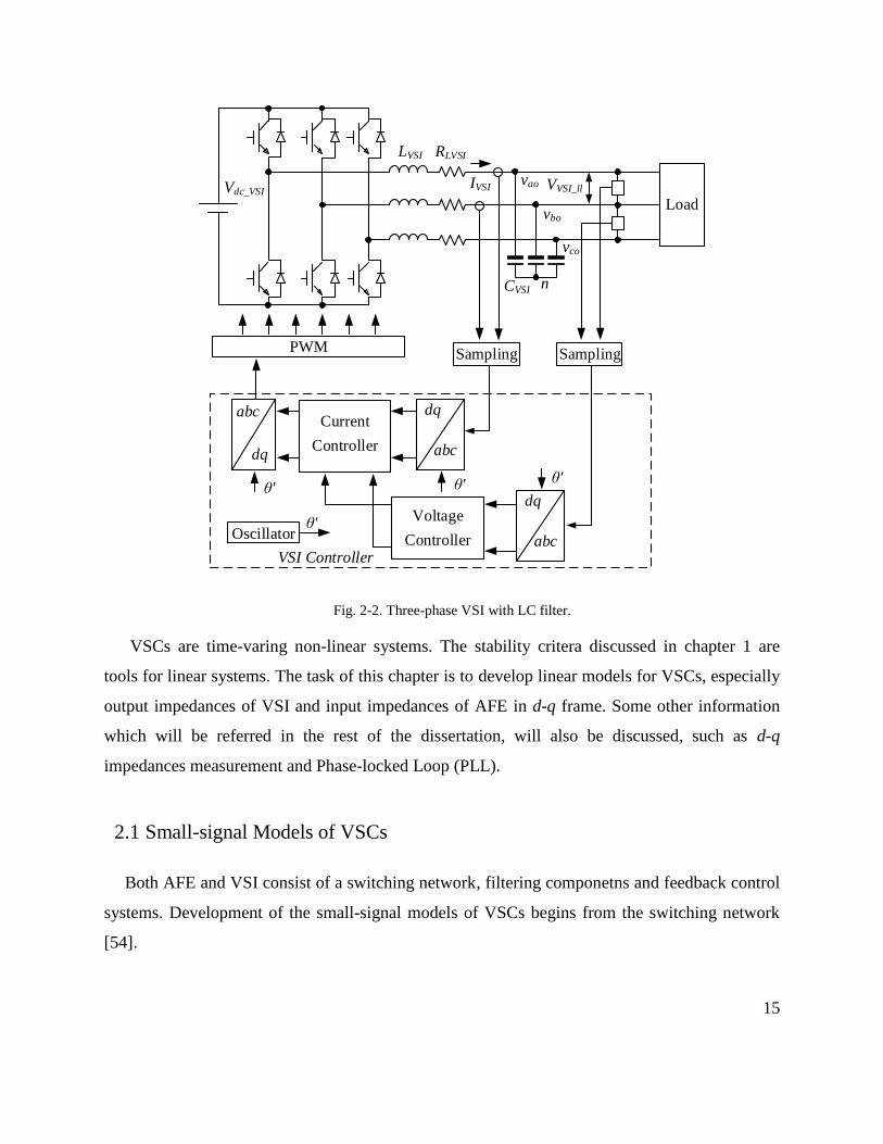
Fig. 2-2. Three-phase VSI with LC filter. ................................................................................ 15
Fig. 2-3. Switching network with ideal swtiches. .................................................................... 16
Fig. 2-4. Switching network with single-pole double-throw switches..................................... 17
Fig. 2-5. Average model of the switching network. ................................................................. 18
Fig. 2-6. Average model of the power stage of VSI. ............................................................... 18
Fig. 2-7. Average equivalent circuit model of VSI. ................................................................. 19
Fig. 2-8. Equivalent circuits of VSI in d-q frame for equilibrium point calculation. .............. 20
Fig. 2-9. Small-signal equivalent circuits model of VSI in d-q frame. .................................... 20
Fig. 2-10. Small-signal equivalent circuits model of AFE in d-q frame. ................................. 21
Fig. 2-11. Flow chart of interrupt function for VSI feedback control...................................... 22

ix
Fig. 2-12. Digital delay caused by digital control algorithm ................................................... 23
Fig. 2-13. Triangular-carrier modulation ................................................................................. 23
Fig. 2-14. Circuit diagram of on board signal conditioning filter. ........................................... 24
Fig. 2-15. Average model of VSI considering delay and signal conditioning filters............... 25
Fig. 2-16. Measurement setup transfer function from dd to id. ................................................. 27
Fig. 2-17. Model and measurement results for open loop transfer functions. ......................... 27
Fig. 2-18. Dead time for the switching network. ..................................................................... 28
Fig. 2-19. Output voltage and inductor current with 2µs dead time. ....................................... 28
Fig. 2-20. Output voltage and inductor current with 1µs dead time and compensation. ......... 29
Fig. 2-21. Influence of dead time to open loop transfer function. ........................................... 29
Fig. 2-22. Current loop-gain measurement setup. .................................................................... 30
Fig. 2-23. Current loop-gains with high BW low PM.............................................................. 31
Fig. 2-24. Output voltage and inductor current with high BW low PM current loop. ............. 31
Fig. 2-25. Current loop-gains with low BW high PM.............................................................. 32
Fig. 2-26. Current reference step responses with high BW low PM........................................ 32
Fig. 2-27. Current reference step responses with low BW high PM........................................ 33
Fig. 2-28. Output voltage and inductor current with low BW high PM current loop. ............. 33
Fig. 2-29. Transfer function from idref to id. ............................................................................. 34
Fig. 2-30. Transfer function from idref to iq. ............................................................................. 34

x
Fig. 2-31. Current controller with decoupling for VSI. ........................................................... 35
Fig. 2-32. Effects of current loop decoupoing control. ............................................................ 35
Fig. 2-33. Transfer function from idref to vd. ............................................................................. 36
Fig. 2-34. Voltage loop-gain. ................................................................................................... 37
Fig. 2-35. Output voltage and inductor with both current and voltage loops. ......................... 37
Fig. 2-36. Voltage reference step responses with both current and voltage loops. .................. 38
Fig. 2-37. Transfer function from vdref to vd. ............................................................................ 38
Fig. 2-38. Voltage controller with decoupling for VSI. ........................................................... 39
Fig. 2-39. Effects of voltage loop decouping control. ............................................................. 39
Fig. 2-40. Average model of VSI in d-q frame with feedback control. ................................... 40
Fig. 2-41. Small-signal circuit model of VSI power stage. ...................................................... 41
Fig. 2-42. VSI power stage small-signal model. ...................................................................... 42
Fig. 2-43. Open loop output impedance of VSI. ...................................................................... 43
Fig. 2-44. VSI small-signal model with current feedback control. .......................................... 44
Fig. 2-45. Inverter output impedance with and without feedback control. .............................. 45
Fig. 2-46. VSI small-signal model with both current and voltage feedback control loops. .... 46
Fig. 2-47. VSI output impedance with single and multiple feedback control loops. ............... 47
Fig. 2-48. Different voltage control loop designs. ................................................................... 48
Fig. 2-49. VSI output impedances with different voltage controllers. ..................................... 48
xi
Fig. 2-50. Small-signal model of AFE. .................................................................................... 49
Fig. 2-51. AFE input impedance in d-q frame. ........................................................................ 50
Fig. 2-52. D-q frame impedance tester..................................................................................... 51
Fig. 2-53. D-q frame impedance measurement. ....................................................................... 52
Fig. 2-54. Measurement setups: (a) output impedances, (b) input impedances. ...................... 55
Fig. 2-55. Measurement results compare with model for open loop. ...................................... 56
Fig. 2-56. Measurement results compare with model for current loop control........................ 56
Fig. 2-57. Measurement results compare with model for voltage control. .............................. 57
Fig. 2-58. SRF PLL. ................................................................................................................. 57
Fig. 2-59. Average model of SRF PLL. ................................................................................... 58
Fig. 2-60. Small-signal model of SRF PLL with ideal grid. .................................................... 58
Fig. 2-61. DDSRF PLL. ........................................................................................................... 59
Fig. 2-62. Average model of DDSRF PLL. ............................................................................. 59
Fig. 3-1. Experimental ac system used for stability analysis. .................................................. 62
Fig. 3-2. Experimental system setup and control scheme. ....................................................... 62
Fig. 3-3. Impedances of VSI and VSC for three cases from average model simulation. ........ 65
Fig. 3-4. Characteristic loci of three cases using simulated impedance from average model. 66
Fig. 3-5. Time domain simulation of interface voltage in d-q frame. ...................................... 67
Fig. 3-6. Test-bed hardware prototype for experimental system. ............................................ 67

xii
Fig. 3-7. Measurement results of case 1. .................................................................................. 70
Fig. 3-8. Measurement results of case 2. .................................................................................. 72
Fig. 3-9. Measurement results of case 3. .................................................................................. 74
Fig. 4-1. Grid-tied inverter with feedback control and PLL. ................................................... 78
Fig. 4-2. Small-signal circuit model of grid-tied inverter in system d-q frame. ...................... 79
Fig. 4-3. Power stage small-signal model. ............................................................................... 80
Fig. 4-4. System and controller d-q frames. ............................................................................. 81
Fig. 4-5. Small-signal model with PLL. ................................................................................... 82
Fig. 4-6. Small-signal model with PLL and current feedback control. .................................... 86
Fig. 4-7. Impedance with current control and different PLL bandwidth. ................................ 88
Fig. 4-8. Phasor diagram interpretation of negative resistor behavior of Zqq. .......................... 88
Fig. 4-9. Impedance with current control and different current ratings. .................................. 89
Fig. 4-10. Impedance with and without decoupling control. ................................................... 90
Fig. 4-11. Impedance with current control and different PLL strategies. ................................ 91
Fig. 4-12. Impedance with different reactive current injections. ............................................. 92
Fig. 4-13. Small-signal model with PLL, current and power feedback control. ...................... 92
Fig. 4-14. Impedance with PLL and power feedback control. ................................................. 94
Fig. 4-15. Impedance with power feedback control and different reactive power injections. . 95
Fig. 4-16. Small-signal model of AFE. .................................................................................... 96

xiii
Fig. 4-17. AFE input impedance with different PLL bandwidth. ............................................ 98
Fig. 4-18. Phasor diagram illustration of AFE Zqq(0). ............................................................. 99
Fig. 4-19. One line diagram of three-phase grid-tied inverter system with local load. ........... 99
Fig. 4-20. (a) PCC voltages; (b) output current of VSI; (c) PLL output frequency of VSI. .. 102
Fig. 4-21. One phase diagram of Zo in stationary frame. ....................................................... 103
Fig. 4-22. Impedances of the source and load. ....................................................................... 105
Fig. 4-23. GNC plots: (a) stable case (kpll = 1.5); (b) unstable case (kpll = 3). ....................... 107
Fig. 4-24. Experimental system. ............................................................................................ 108
Fig. 4-25. Model validation results for idref = -11.A, iqref = 0 A, fbw_PLL = 100 Hz. ................ 111
Fig. 4-26. Model validation results for idref = -11.A, iqref = 0 A. ............................................ 111
Fig. 4-27. Model validation results for idref = -11.A, iqref = 6 A, fbw_PLL = 100 Hz. ................ 113
Fig. 4-28. Model validation results for idref = -11.A, iqref = -6 A, fbw_PLL = 100 Hz. ............... 115
Fig. 4-29. Model validation results for Pdref = -1150 W, Qqref = 0 Var, fbw_PLL = 100 Hz. ..... 117
Fig. 4-30. Model validation results for ZdqAFE....................................................................... 119
Fig. 4-31. Model validation results for YdqAFE ...................................................................... 119
Fig. 4-32. Model validation results with different PLL bandwidth. ...................................... 120
Fig. 5-1. Distribution system with high penetration of VSCs. ............................................... 121
Fig. 5-2. Power stage and control system of VSI. .................................................................. 125
Fig. 5-3. Power stage and control system of AFE.................................................................. 125

xiv
Fig. 5-4. PLL loop-gains for VSI and AFE with ideal grid. .................................................. 127
Fig. 5-5. (a) Grid impedance Zg; (b) Load impedance ZL...................................................... 127
Fig. 5-6. (a) PLLs’ output frequencies; (b) PCC voltages. .................................................... 129
Fig. 5-7. Representations of VSI with local load connecting to the grid. .............................. 129
Fig. 5-8. Representations of VSI and AFE with local load connecting to the grid. ............... 130
Fig. 5-9. Small-signal representation of a dc system. ............................................................ 132
Fig. 5-10. Small-signal representation of a balanced three-phase system in d-q frame......... 132
Fig. 5-11. Small-signal representation of the system under study. ........................................ 134
Fig. 5-12. Grid and VSI impedances for PLL Design 1 and Design 2. ................................. 140
Fig. 5-13. Pole-zero map of VSI (ZVSIdq) and grid side impedances (Zgeqdq). ...................... 140
Fig. 5-14. Characteristic loci of L2 (a) VSI with Design 1; (b) VSI with Design 2............... 142
Fig. 5-15. (a) Standard D contour for L3; (b):Characteristic loci of L3. ................................ 143
Fig. 5-16. VSI PLL loop gains with different PI parameters and ideal grid. ......................... 144
Fig. 5-17. (a) Zqq of grid side and VSI; (b) characteristic loci of L2 with Design 3. ............. 145
Fig. 5-18. (a) PLLs’ output frequencies with Design 3; (b) PCC voltages with Design 3. ... 146
Fig. 5-19. Test-bed hardware prototype for experimental system ......................................... 147
Fig. 5-20. Experimental test results........................................................................................ 148
Fig. 5-21. Grid and VSI impedances for stable and unstable cases. ...................................... 150
Fig. 5-22. Zqq of grid and VSI for stable and unstable cases. ................................................. 152

xv
Fig. 5-23. Characteristic loci of L2 (a) VSI with Design 1; (b) VSI with Design 2............... 153
Fig. 6-1. Three-phase grid-tied PWM inverter system. ......................................................... 156
Fig. 6-2. PLL-based AFD islanding detection method. ......................................................... 156
Fig. 6-3. One line circuit of inverter system under islanding condition. ............................... 157
Fig. 6-4.PLL model under islanding condition. ..................................................................... 157
Fig. 6-5. Impedance-based analysis of inverter system under islanding condition. .............. 159
Fig. 6-6. Load configuration for unintentional islanding test. ............................................... 159
Fig. 6-7. Average model of grid-tied inverter with AFD method. ......................................... 160
Fig. 6-8. Inverter small-signal model with PLL-based AFD method. ................................... 161
Fig. 6-9. Average model of grid-tied inverter with AFD method. ......................................... 161
Fig. 6-10. Average model of SRF PLL. ................................................................................. 162
Fig. 6-11. Output impedance of grid-tied inverter without PLL-based AFD method. .......... 166
Fig. 6-12. Output impedance of grid-tied inverter with PLL-based AFD method. ............... 166
Fig. 6-13. Output impedance of grid-tied inverter with SFS AFD method. .......................... 167
Fig. 6-14. Impedance interaction in qq channel. .................................................................... 168
Fig. 6-15. Characteristic loci of inverter system. ................................................................... 169
Fig. 6-16 Measurement of Zqq for PLL-based AFD method with N = 0.0005. ...................... 170
Fig. 6-17. Measurement of Zqq for SFS AFD method with K = 0.0008. ............................... 171
Fig. 6-18. Islanding event (PLL with feed forward gain N = 0). ........................................... 172

xvi
Fig. 6-19. PLL with feed forward gain N = 0.015 when islanding event happens. ............... 172
Fig. 7-1. Small-signal representation of a balanced three-phase system in d-q frame. .......... 174
Fig. 7-2. Power stage and control system of VSI. .................................................................. 176
Fig. 7-3. Average model of VSI in d-q frame with feedback control. ................................... 177
Fig. 7-4. Non-diagonal feature of impedances matrix of VSI................................................ 178
Fig. 7-5. Capacitor with 1% damping resistor. ...................................................................... 180
Fig. 7-6. VSI open-loop impedances with damping resistor .................................................. 180
Fig. 7-7. Current controller with decoupling for VSI. ........................................................... 181
Fig. 7-8. Voltage controller with decoupling for VSI. ........................................................... 181
Fig. 7-9. VSI small-signal model with feedback control. ...................................................... 182
Fig. 7-10. Output impedances of VSI with and feedback decoupling control. ...................... 182
Fig. 7-11. Power stage and control system of AFE................................................................ 184
Fig. 7-12. AFE input admittances with different PLL bandwidth. ........................................ 185
Fig. 7-13. AFE with input filter. ............................................................................................ 186
Fig. 7-14. LC filter input admittance. ..................................................................................... 190
Fig. 7-15. AFE input impedance with input filter and unity power factor. ........................... 190
Fig. 7-16. Experimental system setup and control scheme. ................................................... 191
Fig. 7-17. Test-bed hardware prototype for experimental system ......................................... 191
Fig. 7-18. Time domain test results of VSI feeding AFE with unity power factor. ............... 192

xvii
Fig. 7-19. Meausred VSI output impedances. ........................................................................ 193
Fig. 7-20. Measured AFE input admittances with unity power factor. .................................. 193
Fig. 7-21. Eigenvalue loci over plotted with impedance ratios.............................................. 194
Fig. 7-22. Measured YdqAFE with input filter. ........................................................................ 194
Fig. 7-23. Eigenvalue loci over plotted with impedance ratios with input filter. .................. 195
Fig. 7-24. Measured YdqAFE (Iq = 90%Id)............................................................................... 196
Fig. 7-25. Eigenvalue loci over plotted with impedance ratios (Iq = 90% Id). ....................... 196
Fig. 7-26. Measured YdqAFE with Vdc_AFE = 320 V. ................................................................ 197
Fig. 7-27. Time domain test results of the system with Vdc_AFE = 320 V. .............................. 198
Fig. 7-28. Eigenvalue loci over plotted with impedance ratios for Test 1 and 4. ................. 198

xviii
LIST OF TABLES
Table 2-1. VSI power stage parameters ................................................................................... 26
Table 3-1. Experimental system parameters. ........................................................................... 63
Table 3-2. Feedback controller parameters for VSI and VSC. ................................................ 65
Table 4-1. Parameters of Grid-Tied Inverter Prototype ........................................................... 87
Table 4-2. Parameters of Current and Power Feedback Controller ......................................... 94
Table 4-3. Parameters of Inverter System for Stability Analysis........................................... 100
Table 4-4. Parameters of AFE system for measurement ....................................................... 118
Table 5-1. Parameters of simulation system .......................................................................... 124
Table 5-2. Parameters of experimental system ...................................................................... 151
Table 6-1. Parameters for simulation and Calculation ........................................................... 164
Table 6-2. Parameters for Experimental Verification ............................................................ 169
Table 7-1. Parameters of simulation system .......................................................................... 179
Table 7-2. Parameters of Test System ................................................................................... 197

1
Chapter 1 Introduction
1.1 Background
Instability was found in aircraft dc power system in the 1950’s. There have been
occasions when energizing a particular inverter has produced an unstable system [1]. In
the 1960’s, instability was found in the 400 Hz electric power system on board US
aircraft carries. A large number of line voltage regulatgors were installed at the aircraft
electric service stations to eliminate voltage losses due to long cables. Upon energization
of all the regulators, the ship power system went into unstable condition [3]. It was found
that the instability is from negative incremental input resistance at power input port of
switching-mode regulator, amplifier, dc-dc converter, or dc-ac inverter [5]. Instability can
be avoid by reducing the regulation bandwidth of the voltage regulator to decrease the
effect of the negative incremental input resistance. From that time, the designers of
distributed power system (DPS) with ac and dc subsystems, as shown in Fig. 1-1, on
various platforms, such as spacecraft [6], space station [7]–[10], more electric aircraft
[11]–[14], automotive system [15], ships [16]–[18], and microgrid [19]–[23], have all paid
close attention to the negative incremental input resistance of regulated converter loads
and its effect on system stability.
…
ac-dc
dc-dc
Ele
ctro
n.
dc-ac
Moto
r
ac-ac
Moto
r
ac bus dc bus
Sola
r
dc-ac
ac-ac
Win
d
dc-dc
Batt
ery
Grid
Zs ZlZs Zl
Pas
sive
Load
Fig. 1-1. Hybrid ac/dc distributed power system.

2
Negative incremental resistance is usually believed due to constant power loads
(CPLs) behavior of power converters. The fast progress of power semiconductors,
especially the wide-bandgap devices [24], [26], [27], enables high switching frequency
(over MHz) and high efficiency[25]–[27] (over 99%) power conversion techniques. With
high switching frequency, regulation bandwidth of power converters can easily reach 1 to
100 kHz range. With a constant output current, high-bandwidth voltage regulation leads
to constant output power. When combined with high conversion efficiency, this results
constant input power characteristic. These converters are then called CPLs. There input
impedances freatures negative incremental resistance [28].
The stability of power systems nonetheless is often analyzed using eigenvalues, which
are extracted from the system matrix “A” of the canonical state space model
representation of the system in question [29]. This approach requires the use of full
dynamic models for all the elements in the system, including physical and control
parameters. As such, DPS integrators need to manage an enormous amount of
information to derive these models; from converter topologies, to circuit parameters, to
control strategies, information that must also be updated every time any of the
components changes in the system. Naturally, the system model needs to be derived
again too. Using this approach, the sharing of proprietary information from different
system component vendors is not feasible, ultimately impeding the proper modeling of
the system.
Loop gain is also a useful stability analysis tool for analog circuit with feedback
control system [32]–[34]. When the phase margin of the loop gain is positive, then the
feedback system is stable. Moreover, increasing the phase margin (could be more than
60°) causes the system transient response to be better behaved, with less overshoot and
ringing. Loop gain can be measured.
However, both eigenvalue and loop gain based stability analysis need information of
components’ inner physical structure and parameters which usually are not available for
system integrator. When components in the system are acquired as “black boxes” for use

3
in bigger electrical system to deliver power from source to load, it may be found that the
system oscillates or becomes unstable because the particular source or load impedances
were not foreseen by the components’ designers; or, the components may have
inadequate input or output filters, so the system integrator has to provide external filters
which in turn may cause the system to oscillate. Under such condition, it is difficult to
use eigenvalue and loop gain based analysis.
As a more practical alternative to the above methods, impedance-based stability
analysis as previously mentioned has been successfully used in dc systems for a long time
[31], where the stability at each interface is determined using measured impedances and
Nyquist stability criterion. The main advantage of this approach is that the measured
impedances intrinsically model all circuit components, including physical components
and control systems. Stability criteria can be formulated then by establishing forbidden
regions in the complex plane where the locus of possible source and load impedance
ratios cannot reside thus ensuring a stable operation [35]–[38]. This allows for new loads
to be added to the system easily without knowing their internal parameters and without
requiring the re-modeling of the whole system to assess its impact on the system stability.
This approach is widely used in design of various dc DPSs, such as spacecraft [6], space
station [7]–[10], more electric aircraft [13], automotive system [15], ships [16]–[18], and
dc microgrid [21].
In terms of three-phase ac systems, negative incremental resistance of CPLs are also
found at the input port of ac-dc converters [3], [39]. Similar impedance-based stability
analysis are formulated in a mathematical framework based on the generalized Nyquist
stability criterion (GNC), reference frame theory, and multivariable control is set forth for
stability assessment [3].
1.1.1 Impedance-based dc system stability analysis
The negative input resistance can be shown to be the result of two properties of power
converters, namely the high regulation bandwidth and high efficiency. It is assumed that
4
the output voltage o
v of the dc-dc converter shown in Fig. 1-2 is maintained constant by
the feedback regulator. If the load current does not change, then o
P is constant. With the
high efficiency of dc-dc converter, i
P is also constant, even if the input voltage dc
v
varies. It follows that if dc
v increases, dc
i must decrease. Consequenctly, the regulator
exhibits a negative incremental input resistance as show in Fig. 1-3. Incombination with
the input filter or the source converter, the negative input resistance can under certain
condition constitute a negative resistance oscillator, and is the origin of the system
potential instability.
Zl
dc-dc
Load
idc
vdc PoPi
+
-
vo
+
-
Fig. 1-2. Dc-dc converter.
VmaxVmin vdc
idcLoad2
PiΔiΔv
ΔvΔi
<0Zl=
Load1
constant
Fig. 1-3. Static input characteristic of dc-dc converter.
5
Zs
Zl
Source Load
vs
vl
Fig. 1-4. Small-signal representation of a dc system.
For dc system, once the system is partitioned to source and load subsystems at an
interface (see Fig. 1-4), stability of the system can be predicted by applying Nyquist
stability criteria to the minor loop-gain (L=Zs/Zl) [28] that is defined by output impedance
(Zs) of the source subsystem and the input impedance (Zl) of load subsystem. Using this
concept, one possible design procedure for the dc subsystem in DPS shown in Fig. 1-1 is
to design the source converter (ac-dc converter in Fig. 1-1) using an unterminated
modeling approach [40]. Then, based on the output impedance characteristics of the
source converter, specification for the input impedance of load subsystem can be defined
to ensure the system stability. Ref. [31] proposes to keep the minor loop-gain loci inside
the unity circle on the complex plane, so that it never encircles the critical point (-1,0),
and the system is stable (if there’s no right half plane (RHP) pole). Transform to
impedance of the system, this concept force the magnitude of the input impedance of the
load subsystem to be larger than the magnitude of the output impedance of the source
subsystem [31]. However, this concept leads to too conservative impedance specification
and bulky input filter for the load subsystem.
To know how stable the system is or how much uncertainty the system design can take,
phase margin (PM) and gain margin (GM) are defined as pointed out in Fig. 1-5 (a). Ref.
[35] proposes a forbidden region concept based on desired PM and GM, as shown in Fig.
1-5 (a), on the complex plane out of which the minor loop-gain shall stay. (Actually,
concept from Ref. [31] is also a forbidden region concept that is the region outside the
unity circle.) The forbidden region shown in Fig. 1-5 (a) can be also transformed to load
impedances (Zl) specification on the Bode plot. As shown in Fig. 1-5 (b), under the

6
frequency range where the magnitude of the load impedance (|Zl|) is higher than the Gain
Limit, which is magnitude of source impedance (|Zs|) plus the GM, there will be no
limitation for the phase of load impedance (∠Zl). However, ∠Zl should stay inside its
valid region (see Fig. 1-5 (b)) in the frequency range where |Zl| is smaller than the Gain
Limit. Compare with the concept proposed by Ref. [31], this forbidden region concept is
less conservative. It allows minor loop-gain loci goes to the outside of unity circle, which
means |Zl| is bigger than |Zs|, but ensure the system stability with certain margin. Since
then, different forbidden region concepts were proposed [36]–[38], and they can be
transformed to certain load impedance specifications. This is a convenient and useful tool
for DPS integrators. Based on the output impedance of source converter, shapes of the
input impedance of load converters can be specified for the suppliers. In this way, not
only the information from suppliers can be protected, but also the system stability can be
assured when source and load are connected by the integrator. This also allows new loads
to be added to the system easily without knowing their internal parameters and without
requiring the re-modeling of the whole system to assess its impact on the system stability.
-1 -0.5 0 0.5 1
-1
-0.5
0
0.5
1
Real
Imag
PM=60°
1/GM
ForbiddenZs Zl/Region
Unity Circle
Mag
nit
ud
e (d
B)
Phas
e (d
eg)
Frequency (Hz)
6 dB
|Zs|
|Zl|
-120°
Valid
region for
-120°
ForbiddenregionZs
Zl
Gain Limit
(a) (b)
Fig. 1-5. (a) Polar plot of minor loop-gain; (b) Bode plot of source and load impedances.
7
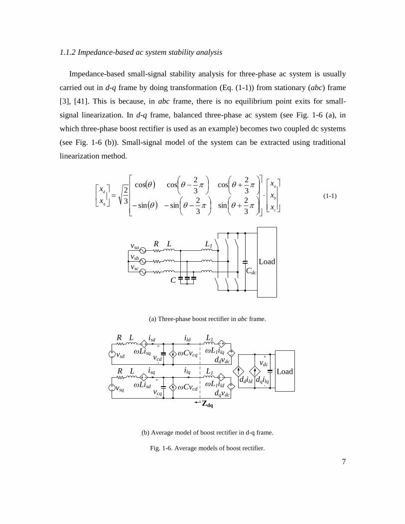
1.1.2 Impedance-based ac system stability analysis
Impedance-based small-signal stability analysis for three-phase ac system is usually
carried out in d-q frame by doing transformation (Eq. (1-1)) from stationary (abc) frame
[3], [41]. This is because, in abc frame, there is no equilibrium point exits for small-
signal linearization. In d-q frame, balanced three-phase ac system (see Fig. 1-6 (a), in
which three-phase boost rectifier is used as an example) becomes two coupled dc systems
(see Fig. 1-6 (b)). Small-signal model of the system can be extracted using traditional
linearization method.
c
b
a
q
d
x
x
x
x
x
3
2sin
3
2sinsin
3
2cos
3
2coscos
3
2 (1-1)
L1
Cdc
vsa
vsb
vsc
LR
C
Load
(a) Three-phase boost rectifier in abc frame.
vsd
vsq
isq
isd
ilq
ild
vcd
+
-
vcq
+
-
ωLisq
R
ωLisd ωCvcd
ωCvcq
L
R L L1
L1
Load
vdc
+
-
ωL1ilq
ωL1ild
ddvdc
dqvdc
ddild dqilq
Zdq
(b) Average model of boost rectifier in d-q frame.
Fig. 1-6. Average models of boost rectifier.

8
Different from impedances of dc-dc converters, impedances of three-phase ac
converters are 2×2 matrices as shown by Eq. (1-2). This is due to the coupling effect
between d-axis and q-axis.
sZsZ
sZsZs
qqqd
dqdd
dqZ (1-2)
In ac system, the negative resistor behavior is observed in the Zdd element of the
rectifier (Fig. 1-6 (b)) input impedance that also acts as a constant power load [39], as a
result of which instability can be induced in the ac system due to the negative resistance
of Zdd.
Similar to dc system, the balanced three-phase ac system can be then presented by
source and load subsystems as shown in Fig. 1-7.
Zsdq
Yldq
Source Load
vs→
vl→
Fig. 1-7. Small-signal representation of a balanced three-phase system in d-q frame.
Similar to dc system, the interface voltage (l
v
) can be derived as Eq. (1-3). Minor
loop-gain is defined as Eq. (1-4), which is the ratio between source and load impedances
in d-q frame.
)()()()( svsssvsl
1
ldqsdqYZI
(1-3)
)()()( sssldqsdq
YZL (1-4)
9
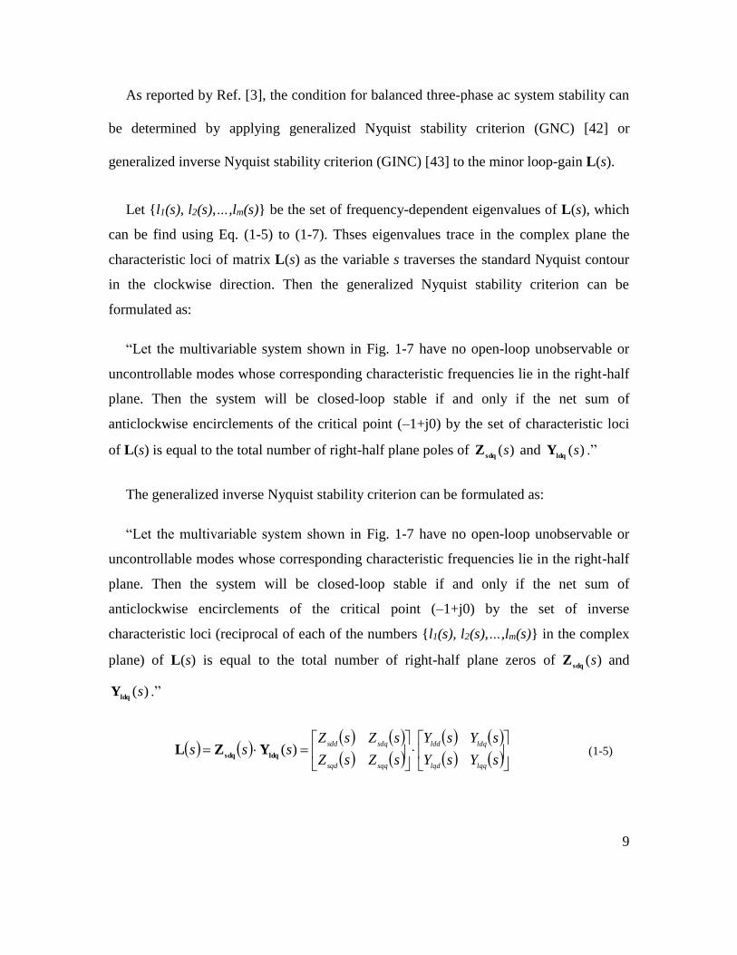
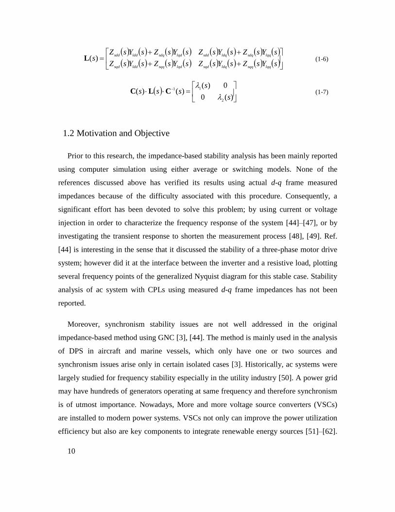
As reported by Ref. [3], the condition for balanced three-phase ac system stability can
be determined by applying generalized Nyquist stability criterion (GNC) [42] or
generalized inverse Nyquist stability criterion (GINC) [43] to the minor loop-gain L(s).
Let l1(s), l2(s),…,lm(s) be the set of frequency-dependent eigenvalues of L(s), which
can be find using Eq. (1-5) to (1-7). Thses eigenvalues trace in the complex plane the
characteristic loci of matrix L(s) as the variable s traverses the standard Nyquist contour
in the clockwise direction. Then the generalized Nyquist stability criterion can be
formulated as:
“Let the multivariable system shown in Fig. 1-7 have no open-loop unobservable or
uncontrollable modes whose corresponding characteristic frequencies lie in the right-half
plane. Then the system will be closed-loop stable if and only if the net sum of
anticlockwise encirclements of the critical point (–1+j0) by the set of characteristic loci
of L(s) is equal to the total number of right-half plane poles of )(ssdq
Z and )(sldq
Y .”
The generalized inverse Nyquist stability criterion can be formulated as:
“Let the multivariable system shown in Fig. 1-7 have no open-loop unobservable or
uncontrollable modes whose corresponding characteristic frequencies lie in the right-half
plane. Then the system will be closed-loop stable if and only if the net sum of
anticlockwise encirclements of the critical point (–1+j0) by the set of inverse
characteristic loci (reciprocal of each of the numbers l1(s), l2(s),…,lm(s) in the complex
plane) of L(s) is equal to the total number of right-half plane zeros of )(ssdq
Z and
)(sldq
Y .”
sYsY
sYsY
sZsZ
sZsZsss
lqqlqd
ldqldd
sqqsqd
sdqsdd)(
ldqsdqYZL (1-5)
10
sYsZsYsZsYsZsYsZ
sYsZsYsZsYsZsYsZs
lqqsqqldqsqdlqdsqqlddsqd
lqqsdqldqsddlqdsdqlddsdd)(L (1-6)
)(0
0)()()(
2
11
s
ssss
CLC (1-7)
1.2 Motivation and Objective
Prior to this research, the impedance-based stability analysis has been mainly reported
using computer simulation using either average or switching models. None of the
references discussed above has verified its results using actual d-q frame measured
impedances because of the difficulty associated with this procedure. Consequently, a
significant effort has been devoted to solve this problem; by using current or voltage
injection in order to characterize the frequency response of the system [44]–[47], or by
investigating the transient response to shorten the measurement process [48], [49]. Ref.
[44] is interesting in the sense that it discussed the stability of a three-phase motor drive
system; however did it at the interface between the inverter and a resistive load, plotting
several frequency points of the generalized Nyquist diagram for this stable case. Stability
analysis of ac system with CPLs using measured d-q frame impedances has not been
reported.
Moreover, synchronism stability issues are not well addressed in the original
impedance-based method using GNC [3], [44]. The method is mainly used in the analysis
of DPS in aircraft and marine vessels, which only have one or two sources and
synchronism issues arise only in certain isolated cases [3]. Historically, ac systems were
largely studied for frequency stability especially in the utility industry [50]. A power grid
may have hundreds of generators operating at same frequency and therefore synchronism
is of utmost importance. Nowadays, More and more voltage source converters (VSCs)
are installed to modern power systems. VSCs not only can improve the power utilization
efficiency but also are key components to integrate renewable energy sources [51]–[62].

11
VSCs should also synchronize with the grid. Phase-locked loops (PLLs) [63], [64] are
standard techniques for synchronization. Some literatures have reported that PLL has a
negative impact mainly in the inverter mode [65]–[67]. Synchronism issues between
parallel-connected VSCs with weak grid are also reported [68]. However, influence of
PLL on impedances of VSCs is not well discussed, and the synchronism issues caused by
PLL is not analyzed using impedance-based method.
Although GNC utilizes minor loop-gain L(s) defined by source and load impedances
matrices. Elements of L(s) are functions of both self-channel and cross-channel
impedances ratios as show in Eq. (1-5) and (1-6). Plus, stability condition is finally
judged by eigenvalues of L(s). If L(s) is non-diagonal, finding eigenvalues for non-
diagonal matrix will involve complicated computation, which makes indirect relationship
between system stability condition and impedances. This is the roadblock of doing load
impedance specification for ac system in d-q frame. Based on the relationship between a
matrix’s eigenvalues and its singular values, Ref. [69] proposes to limit the minimum
singular value of load input impedance matrix to be smaller than the maximum singular
value of the source output impedance. This concept is similar as the one in Ref. [28] for
dc system, which leads to conservative design. Load impedances specification, which can
greatly help system integration, in ac system that allows impedance interaction but still
keep the system stable with certain margin is not reported yet.
Addressing these unexplored issues, this research investigates the small-signal
stability of three-phase ac systems with CPLs using measured d-q frame impedances.
Prior to this research, negative incremental resistance is only found in CPLs as a results
of output voltage regulation. In this research, negative incremental resistance is
discovered in grid-tied inverters as a consequence of grid synchronization. Based on the
negative incremental resistance concept of grid-tied inverters, grid synchronization
stability issues are well explained under the framework of GNC. Moreover, this research
finds out that under unity power factor condition, three-phase ac system is diagonal. It
can be simplified to two decoupled dc systems. Load impedances can be then specificed
to guarantee system stability and less conservative design.
12
1.3 Disseration Outline and Summary of Contributions
Three-phase VSCs are basic building blocks for many DPS. Stability issues discussed
in this dissertation happen between different types of VSCs. Chapter 2 discusses the
small-signal models for different VSCs, such as inverters and rectifiers. Impedances
matrices in d-q frame are derived based on the results in the literature. Some VSCs need
PLL to synchronize with the ac bus, basic PLL structures and models for grid-tied VSCs
are also discussed in this chapter.
Chapter 3 presents, for the first time, the small-signal stability analysis of a balanced
three-phase ac system with constant power loads based on the GNC and measured
impedances in d-q frame. The results obtained show how the stability at the ac interface
can be easily and readily predicted using the measured impedances and the GNC; thus
illustrating the practicality of the approach, and validating the use of ac impedances as a
valuable dynamic analysis tool for ac system integration.
Chapter 4 proposes a full analytical model for the output impedance of the three-phase
grid-tied VSCs considering the effect of PLL. The result unveils an interesting and
important feature of three-phase grid-tied VSCs, namely that its q-q channel impedance
(Zqq) behaves as a negative incremental resistor for inverter and a positive incremental
resistor for rectifier. Moreover, this behavior is a consequence of grid synchronization,
where the bandwidth of the PLL determines the frequency range of the incremental
resistor behavior, and the power rating of VSCs determines the magnitude of the resistor.
In addition, PLL-based active frequency drift islanding detection (AFD) function makes
phase of Zqq of grid-tied inverter drops below -180°, which has worse impact than the
negative resistance in the system stability point of view.
Chapter 5 discusses the stability issues caused by PLL dynamics. Due to the PLL
dynamics, parallel connected VSCs could lose synchronization under weak grid
condition. This issue is well studied in this chapter within the frame work of impedance-
based analysis using GNC.

13
Chapter 6 presented an impedance-based analysis for active frequency drift islanding
detection methods. The output impedance of a grid-tied inverter was modeled with PLL-
based AFD method. With big feed forward gain N for islanding detection, the phase of
Zqq is shown to drop below –180°. Under islanding condition, the inverter system became
unstable with a frequency drift away from steady-state. Based on the impedance of the
inverter, it could be concluded that the grid-tied inverter with AFD islanding method has
the potential to destabilize the grid-connected inverter system when the grid is weak.
Chapter 7 proposes impedances specification for balanced three-phase ac DPSs. Under
unity power factor condition, three-phase ac system is diagonal. It can be simplified to
two decoupled dc systems. Load impedances can be then specificed to guarantee system
stability and less conservative design.
The last chapter summarizes the work and discusses some possible future work.

STABILITY ANALYSIS OF THREE-PHASE AC POWER SYSTEMS BASED ON MEASURED D-Q FRAME IMPEDANCES
14
Chapter 2 Modeling of Voltage Source Converters
More and more voltage source converters (VSCs) are installed to modern power systems.
VSCs not only can improve the power utilization efficiency but also are key components to
integrate new energy sources. For example, in the power distribution system with high
penetration of power electronics and renewable energy, as shown in Fig. 1-1, three-phase pulse-
width modulated (PWM) rectifiers, as shown in Fig. 2-1, which have better efficiency and power
quality performance [51], [52], are installed working as active front end (AFE) to replace
conventional line-commutated converters for motor drives. Three-phase voltage source inverters
(VSIs) with output voltage control, as shown in Fig. 2-2, are installed to provide power to the
factory and building when the grid is gone. Grid-tied VSIs with only current controllers are used
to delivery power from wind turbines or solar panels to the grid [62].
PWM
AFE ControllerPLLvabc
SamplingSampling
abc
dq
abc
dq
abc
dq
Voltage
Controller
Current
Controller
LAFERLAFE
Cdc_AFE
θ θθ
Vdc_AFE
IAFE
n Load
Fig. 2-1. Three-phase boost rectifier.
15
abc
dq
dq
abc
PWM
VSI Controller
Sampling Sampling
abc
dqVoltage
Controller
Current
Controller
Oscillator
LVSI RLVSI
Vdc_VSI
θ'
θ'
θ' θ'
IVSI
Load
CVSI
VVSI_ll
n
vao
vbo
vco
Fig. 2-2. Three-phase VSI with LC filter.
VSCs are time-varing non-linear systems. The stability critera discussed in chapter 1 are
tools for linear systems. The task of this chapter is to develop linear models for VSCs, especially
output impedances of VSI and input impedances of AFE in d-q frame. Some other information
which will be referred in the rest of the dissertation, will also be discussed, such as d-q
impedances measurement and Phase-locked Loop (PLL).
2.1 Small-signal Models of VSCs
Both AFE and VSI consist of a switching network, filtering componetns and feedback control
systems. Development of the small-signal models of VSCs begins from the switching network
[54].
STABILITY ANALYSIS OF THREE-PHASE AC POWER SYSTEMS BASED ON MEASURED D-Q FRAME IMPEDANCES
16
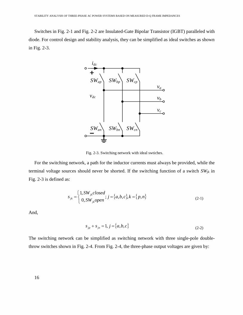
Switches in Fig. 2-1 and Fig. 2-2 are Insulated-Gate Bipolar Transistor (IGBT) paralleled with
diode. For control design and stability analysis, they can be simplified as ideal switches as shown
in Fig. 2-3.
vdc
idc
va
vb
vc
SWap SWbp SWcp
SWan SWbn SWcn
Fig. 2-3. Switching network with ideal swtiches.
For the switching network, a path for the inductor currents must always be provided, while the
terminal voltage sources should never be shorted. If the switching function of a switch SWjk in
Fig. 2-3 is defined as:
npkcbajopenSW
closedSWs
jk
jk
jk ,,,,;,0
,1
(2-1)
And,
cbajss jnjp ,,,1 (2-2)
The switching network can be simplified as switching network with three single-pole double-
throw switches shown in Fig. 2-4. From Fig. 2-4, the three-phase output voltages are given by:
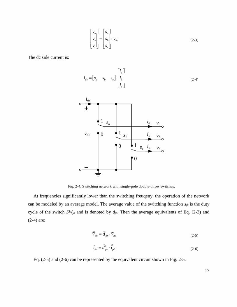
17
dc
c
b
a
c
b
a
v
s
s
s
v
v
v
(2-3)
The dc side current is:
c
b
a
cbadc
i
i
i
sssi (2-4)
vdc
idc
va
vb
vc
ia
ib
ic
1
0 1
0 1
0
sa
sb
sc
Fig. 2-4. Switching network with single-pole double-throw switches.
At frequencies significantly lower than the switching freuqeny, the operation of the network
can be modeled by an average model. The average value of the switching function sjk is the duty
cycle of the switch SWjk and is denoted by djk. Then the average equivalents of Eq. (2-3) and
(2-4) are:
dcphph vdv
(2-5)
phphdc idi (2-6)
Eq. (2-5) and (2-6) can be represented by the equivalent circuit shown in Fig. 2-5.

STABILITY ANALYSIS OF THREE-PHASE AC POWER SYSTEMS BASED ON MEASURED D-Q FRAME IMPEDANCES
18
idc
vdc
dc icdbibdaia
vdc da
ia
vdc db
ib
vdc dc
ic
Fig. 2-5. Average model of the switching network.
idc
vdc
dc icdb ibda ia
ia
ib
ic
CVSIRLVSILVSI
CVSI
CVSI
RLVSILVSI
RLVSILVSI
vdcda+db+dc
3
vdcda+db+dc
3
vdcda+db+dc
3dbvdc
davdc
dcvdc
RL
RL
RL
vao
vbo
vco
Fig. 2-6. Average model of the power stage of VSI.
To get the average model of VSCs’ power stage, just connect the average model of switching
network with the filters as shown in Fig. 2-6 for the case of VSI. In Fig. 2-6, the neutral point
voltage is modeled as:
dccbacba
n vdddvvv
v
3
1
3 (2-7)
19
The state-space equations of Fig. 2-6 are:
phophdc
phdcphLVSI
ph
VSI vdv
dviRdt
idL
111
111
111
3 (2-8)
pho
L
ph
pho
VSI vR
idt
vdC
1 (2-9)
phphdc idi (2-10)
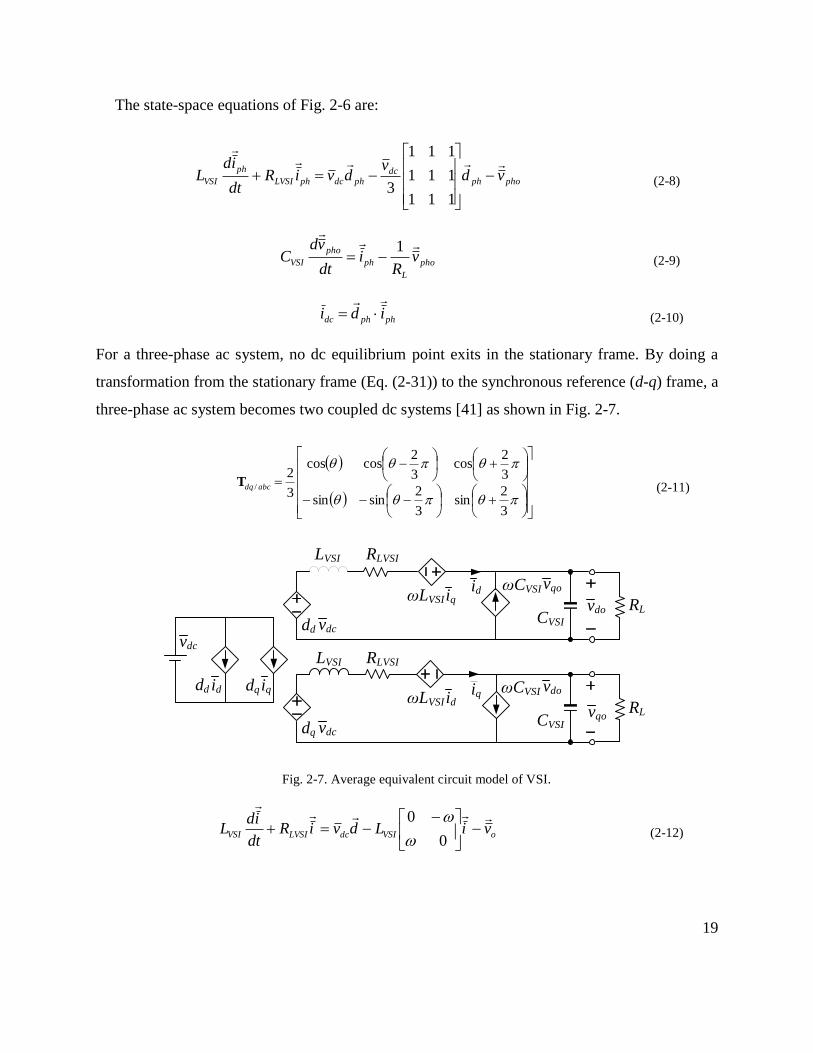
For a three-phase ac system, no dc equilibrium point exits in the stationary frame. By doing a
transformation from the stationary frame (Eq. (2-31)) to the synchronous reference (d-q) frame, a
three-phase ac system becomes two coupled dc systems [41] as shown in Fig. 2-7.
3
2sin
3
2sinsin
3
2cos
3
2coscos
3
2/ abcdqT
(2-11)
LVSI
iq
LVSI
id
CVSI
RLVSI
RLVSI
dd ωCVSI
CVSI
ωCVSI
vdo
vqo
dqωLVSI id
ωLVSIiq
id iq
vdc
dq vdc
dd vdc
vqo
vdo
RL
RL
Fig. 2-7. Average equivalent circuit model of VSI.
oVSIdcLVSIVSI viLdviRdt
idL
0
0
(2-12)
STABILITY ANALYSIS OF THREE-PHASE AC POWER SYSTEMS BASED ON MEASURED D-Q FRAME IMPEDANCES
20
oVSIo
L
oVSI vCv
Ri
dt
vdC
0
01
(2-13)
ididc
(2-14)
Iq
Id
RLVSI
RLVSI
Dd ωCVSI
ωCVSI
Vdo
Vqo
DqωLVSIId
ωLVSIIq
Id Iq
Vdc
DdVdc
Vqo
Vdo
RL
RL
DqVdc
Fig. 2-8. Equivalent circuits of VSI in d-q frame for equilibrium point calculation.
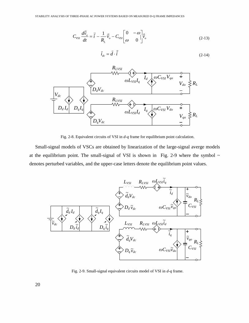
Small-signal models of VSCs are obtained by linearization of the large-signal averge models
at the equilibrium point. The small-signal of VSI is shown in Fig. 2-9 where the symbol ~
denotes perturbed variables, and the upper-case letters denote the equilibrium point values.
id~
iq
~
LVSI RLVSI
LVSI RLVSI
CVSI
CVSI
Vdcdq
~
Dq
~vdc
Iddd
~
Dd id~
Iqdq
~
Dq iq~
~vdc
vdo~
vqo~
Dd~vdc
Vdcdd
~
ωLVSIiq~
ωLVSIid~
ωCVSIvdo~
ωCVSIvqo~
RL
RL
Fig. 2-9. Small-signal equivalent circuits model of VSI in d-q frame.
21
LAFE
LAFE
idc
~
Cdc_AFE
Rdc
id~
iq
~ iqDq~
Iqdq
~idDd
~Iddd
~
Ddvdc_AFE~
Vdc_AFEdd
~
Dqvdc_AFE~
Vdc_AFEdq
~
RLAFE
RLAFE
ωLAFEiq~
ωLAFEid~
vdc_AFE~
vdo~
vqo~
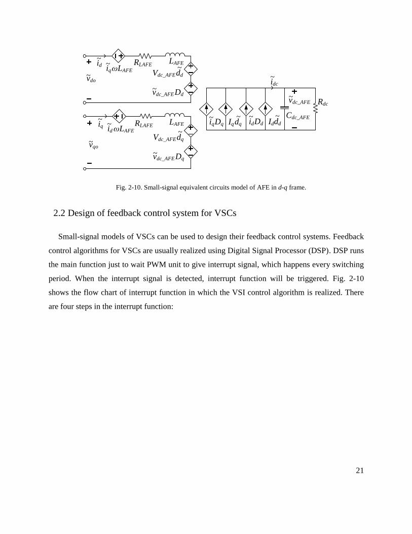
Fig. 2-10. Small-signal equivalent circuits model of AFE in d-q frame.
2.2 Design of feedback control system for VSCs
Small-signal models of VSCs can be used to design their feedback control systems. Feedback
control algorithms for VSCs are usually realized using Digital Signal Processor (DSP). DSP runs
the main function just to wait PWM unit to give interrupt signal, which happens every switching
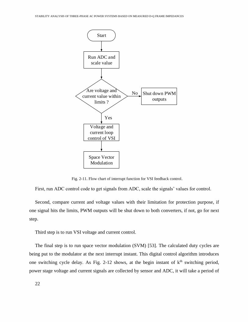
period. When the interrupt signal is detected, interrupt function will be triggered. Fig. 2-10
shows the flow chart of interrupt function in which the VSI control algorithm is realized. There
are four steps in the interrupt function:
STABILITY ANALYSIS OF THREE-PHASE AC POWER SYSTEMS BASED ON MEASURED D-Q FRAME IMPEDANCES
22
Start
Run ADC and
scale value
Are voltage and
current value within
limits ?
Voltage and
current loop
control of VSI
Shut down PWM
outputs
Space Vector
Modulation
No
Yes
Fig. 2-11. Flow chart of interrupt function for VSI feedback control.
First, run ADC control code to get signals from ADC, scale the signals’ values for control.
Second, compare current and voltage values with their limitation for protection purpose, if
one signal hits the limits, PWM outputs will be shut down to both converters, if not, go for next
step.
Third step is to run VSI voltage and current control.
The final step is to run space vector modulation (SVM) [53]. The calculated duty cycles are
being put to the modulator at the next interrupt instant. This digital control algorithm introduces
one switching cycle delay. As Fig. 2-12 shows, at the begin instant of kth switching period,
power stage voltage and current signals are collected by sensor and ADC, it will take a period of

23
time for ADC to finish conversion. The digital processor then take some time to run the feedback
control and SVM algorithm, the results of the computation will be updated to the modulator’s
registers at the beginning of (k+1)th switching period. In this process, the computation results of
kth switching instant is update at the (k+1)th switching instant, this yields a switching period
delay. The triangular-carrier modulation is used as being shows in Fig. 2-13. The modulator will
introduce additional half switching cycle (Tsw) delay according to [55].
(k+1)TskTs
Duty cycle
update
Sampling
instantAD
conversionComputation
Ts
Fig. 2-12. Digital delay caused by digital control algorithm
(k+1)Ts (k+2)Ts
da(,b,c)(t)
sa
sb
sc
Fig. 2-13. Triangular-carrier modulation
STABILITY ANALYSIS OF THREE-PHASE AC POWER SYSTEMS BASED ON MEASURED D-Q FRAME IMPEDANCES
24
The small-signal of the delay caused by digitial controller and PWM can be model as Eq.
(2-15) [56].
sT
sT
sT
sT
del
del
del
del
5.01
5.010
05.01
5.01
delG (2-15)
swdel TT 5.1 (2-16)
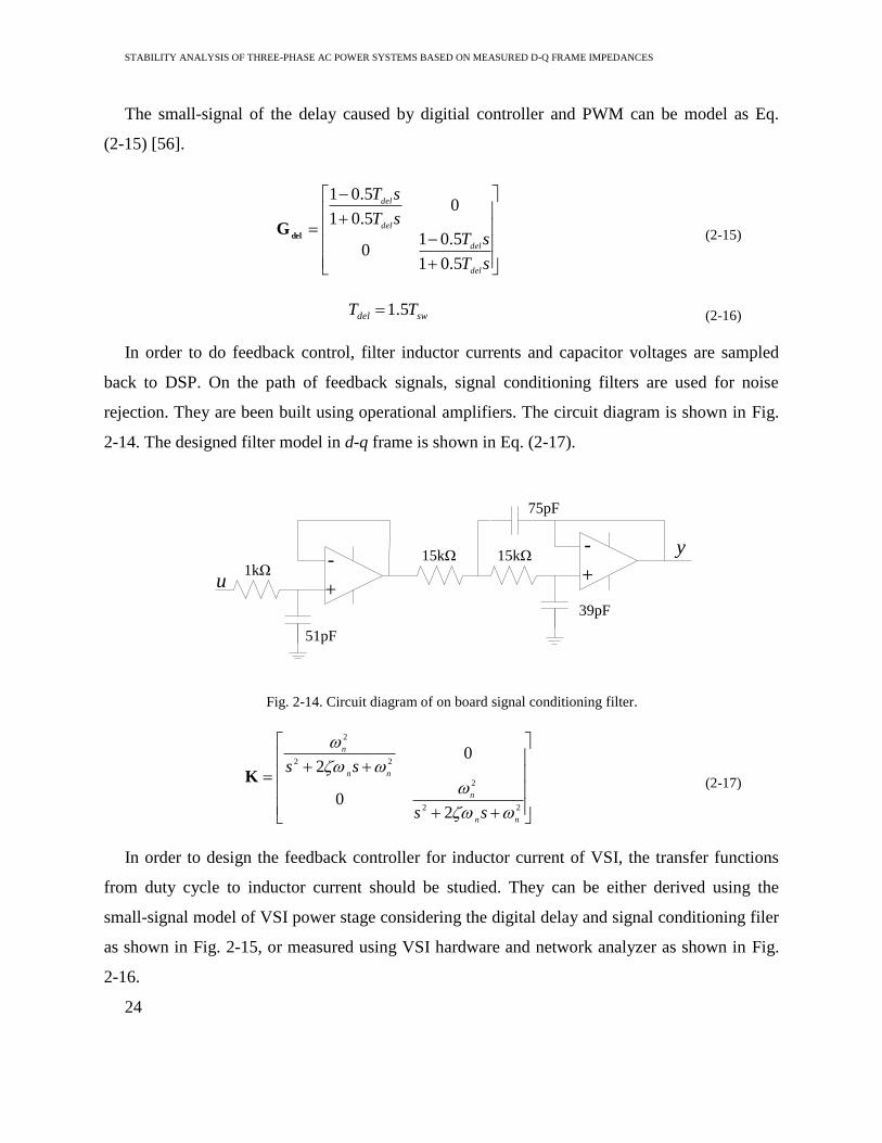
In order to do feedback control, filter inductor currents and capacitor voltages are sampled
back to DSP. On the path of feedback signals, signal conditioning filters are used for noise
rejection. They are been built using operational amplifiers. The circuit diagram is shown in Fig.
2-14. The designed filter model in d-q frame is shown in Eq. (2-17).
-
+
-
+1kΩ
51pF
15kΩ 15kΩ
75pF
39pF
u
y
Fig. 2-14. Circuit diagram of on board signal conditioning filter.
22
2
22
2
20
02
nn
n
nn
n
ss
ss
K (2-17)
In order to design the feedback controller for inductor current of VSI, the transfer functions
from duty cycle to inductor current should be studied. They can be either derived using the
small-signal model of VSI power stage considering the digital delay and signal conditioning filer
as shown in Fig. 2-15, or measured using VSI hardware and network analyzer as shown in Fig.
2-16.

25
id~
iq
~
LVSI RLVSI
LVSI RLVSI
CVSI
CVSI
Vdcdq
~
Dq
~vdc
Iddd
~
Dd id~
Iqdq
~
Dq iq~
~vdc
vdo~
vqo~
Dd~vdc
Vdcdd
~
ωLVSIiq~
ωLVSIid~
ωCVSIvdo~
ωCVSIvqo~
RL
RL
Gdel
dd
~
dq
~dq
~ c
cdd
~
Kiq
~id
~cid
~
iq
~ c
Fig. 2-15. Average model of VSI considering delay and signal conditioning filters.
Fig. 2-16 shows the measurement setups of VSI d channel duty cycle (dd) to d channel current
(id) transfer function. Network analyzer 4395A is being used for this measurement. First, 4395A
generate small signal perturbation, this perturbation is connected to digital controller, which is
used to control power stage of VSI, after analog to digital conversion, and the perturbation is
added to d channel duty cycle reference Dref. Duty ratios in d-q frame are then transferred to α-β
frame for SVM. Small-signal perturbation propagates to gate commands for the power module
and further to the voltage generated by the power module at the each phase-leg middle point.
When the perturbed voltage applied to the output LC filter and resistor load, the current of the
inductors are perturbed. These currents are collected back to digital processor and transferred to
d-q frame. The perturbed d channel duty ratio and d channel current are sent back to network
analyzer by digital to analog converter. Network analyzer then measures the transfer function
from dd to id. To measure the transfer function from dq to iq, same procedure can be followed.
The only change is to apply the perturbation to Dqref and collect perturbed dq and iq back to
network analyzer.

STABILITY ANALYSIS OF THREE-PHASE AC POWER SYSTEMS BASED ON MEASURED D-Q FRAME IMPEDANCES
26
Table 2-1. VSI power stage parameters
Symbol Description Value
Vdc VSI input dc voltage 270 V
VVSI_ll VSI output line-line rms voltage 99.6 V
f VSI output voltage frequency 400 Hz
LVSI Inductance of VSI output inductor 970 µH
RLVSI Output inductor self-resistor 120 mΩ
CVSI VSI output capacitor 32 µF
fsw Switching frequency 20 kHz
RL Load resistor 15 Ω
Tdel Control and PWM delay 1.5/fsw
ωn Natural frequency of signal conditioning filter 1.23e6 rad/s
ζ Damping factor of signal conditioning filter 4.74e-13
Ddref D channel duty cycle reference 0.2996
Dqref Q channel duty cycle reference 0.0662

27
LVSI
CVSI
RL
Vdc_VSI
ADC
DAC
4395A
abc
dq+
ADC
DAC
dq
abc
PWM
DdrefDqref
+
Filter
DSP
RLVSI
n
Fig. 2-16. Measurement setup transfer function from dd to id.
-20
0
20
40
-180
0
180
-20
0
20
40
-180
0
180
Frequency (Hz)10
410
310
210
410
310
2
Mag
.
(dB
)
Phas
e
(deg
)
Mag
.
(dB
)
Phas
e
(deg
)
tfid_dd tfid_dq
tfiq_dd tfiq_dq
ModelMeasurement
Fig. 2-17. Model and measurement results for open loop transfer functions.
STABILITY ANALYSIS OF THREE-PHASE AC POWER SYSTEMS BASED ON MEASURED D-Q FRAME IMPEDANCES
28
Using the VSI parameters list in Table 2-1, transfer functions from duty cycle to inductor
currents are calculated using the model discussed before. Also, they are measured using the
method described in Fig. 2-16. Comparison between results from small-signal model and
measured are shown in Fig. 2-17. They match with each other with good accuracy.
sap
san
Dead time1
0
1
0
Fig. 2-18. Dead time for the switching network.
vabo
ia
Fig. 2-19. Output voltage and inductor current with 2µs dead time.
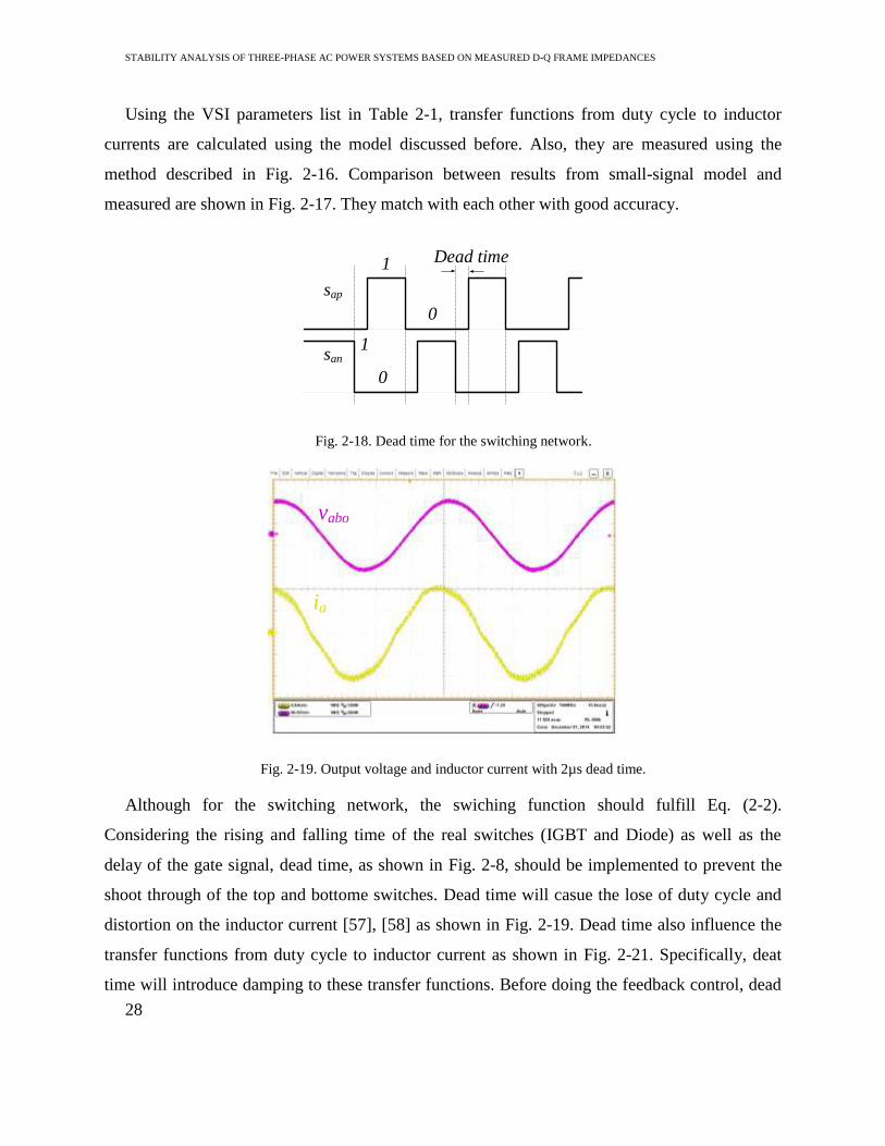
Although for the switching network, the swiching function should fulfill Eq. (2-2).
Considering the rising and falling time of the real switches (IGBT and Diode) as well as the
delay of the gate signal, dead time, as shown in Fig. 2-8, should be implemented to prevent the
shoot through of the top and bottome switches. Dead time will casue the lose of duty cycle and
distortion on the inductor current [57], [58] as shown in Fig. 2-19. Dead time also influence the
transfer functions from duty cycle to inductor current as shown in Fig. 2-21. Specifically, deat
time will introduce damping to these transfer functions. Before doing the feedback control, dead
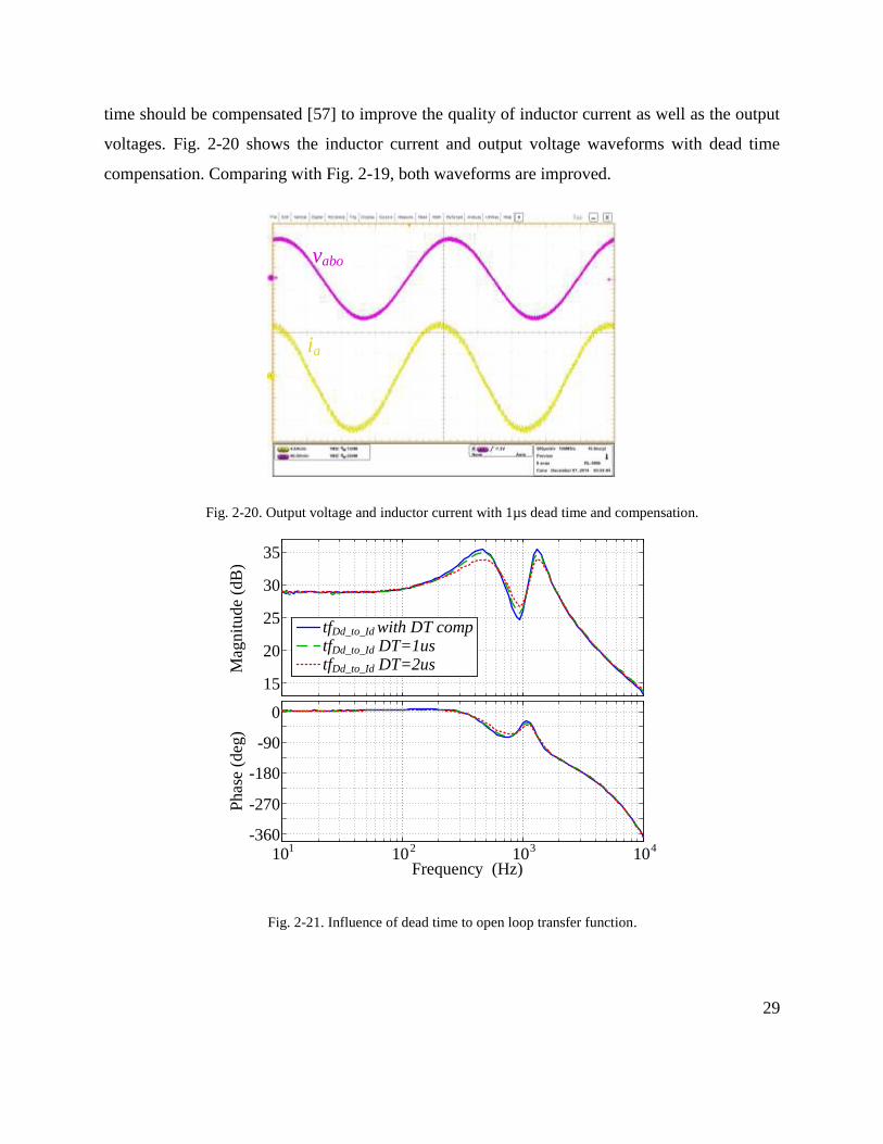
29
time should be compensated [57] to improve the quality of inductor current as well as the output
voltages. Fig. 2-20 shows the inductor current and output voltage waveforms with dead time
compensation. Comparing with Fig. 2-19, both waveforms are improved.
vabo
ia
Fig. 2-20. Output voltage and inductor current with 1µs dead time and compensation.
Frequency (Hz)10
110
210
410
3
Mag
nit
ud
e (d
B)
Phas
e (d
eg)
15
20
25
30
35
-360
-270
-180
-90
0
tfDd_to_Id DT=2ustfDd_to_Id DT=1ustfDd_to_Id with DT comp
Fig. 2-21. Influence of dead time to open loop transfer function.

STABILITY ANALYSIS OF THREE-PHASE AC POWER SYSTEMS BASED ON MEASURED D-Q FRAME IMPEDANCES
30
Based on the transfer functions been measured, PI controller (kpi = 0.0465; kii = 121.01) is
designed. Fig. 2-22 shows the d channel current feedback control loop-gain measurement setup.
Current loop-gain is measured by breaking the feedback control loop and injecting perturbation
using network analyzer. The breaking point is chosen at the feedback signal id, the signals before
and after adding perturbation are sent out to network analyzer to measure the loop-gain. Fig.
2-23 shows the small-signal model and measurement results of d and q channel current loop-
gains. The comparison shows the simulation results match the measurement results very well.
LVSI
CVSI
RL
Vdc_VSI
PWM
Filter
RLVSI
n
ADC
DAC
4395A
abc
dq+
+
ADC
PI
DAC
PI
idref
iqref
-
-+
dq
abc
DSP
Fig. 2-22. Current loop-gain measurement setup.
Notice that the current loop-gains in Fig. 2-23 have 2k Hz bandwidth (BW) and 21° phase
margin (PM). This design has small PM which is not enough for typical feedback control loop.
The inductor current can be distorted because of the small PM as shown in Fig. 2-24. To reduce
the resonance in the inductor current and improve the quality of the waveform, a current
regulator with high PM can help.
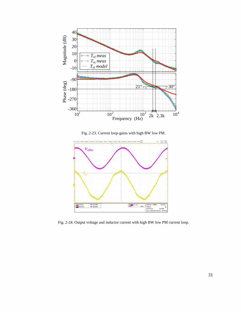
31
Tid meas
Tiq meas
Tid model-10
0
10
20
30
40
-360
-270
-180
-90
Frequency (Hz)10
110
210
410
3
Mag
nit
ud
e (d
B)
Phas
e (d
eg)
2k 2.3k
21° 30°
Fig. 2-23. Current loop-gains with high BW low PM.
vabo
ia
Fig. 2-24. Output voltage and inductor current with high BW low PM current loop.
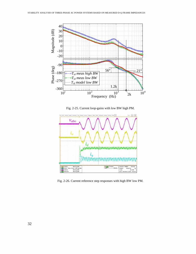
STABILITY ANALYSIS OF THREE-PHASE AC POWER SYSTEMS BASED ON MEASURED D-Q FRAME IMPEDANCES
32
-360
-270
-180
-90
-20
-10
0
10
20
30
40
Frequency (Hz)10
110
210
410
3
Mag
nit
ud
e (d
B)
Ph
ase
(deg
)
Tid model low BW
Tid meas low BW
Tid meas high BW
1.2k
2k
21°56°
Fig. 2-25. Current loop-gains with low BW high PM.
vabo
ia
id
iq
Fig. 2-26. Current reference step responses with high BW low PM.

33
vabo
ia
id
iq
Fig. 2-27. Current reference step responses with low BW high PM.
vabo
ia
Fig. 2-28. Output voltage and inductor current with low BW high PM current loop.
By reducing the value of current loop PI controller by half, the PM of the loop-gains can be
increased as shown in Fig. 2-25. In Fig. 2-25, the BW is still around 1k Hz, the PM is increased
to 56°. With this design, the current loop has more robustness and the quality of the current
waveform is improved as shown in Fig. 2-27 and Fig. 2-28.

STABILITY ANALYSIS OF THREE-PHASE AC POWER SYSTEMS BASED ON MEASURED D-Q FRAME IMPEDANCES
34
Frequency (Hz)10
110
210
410
3
Mag
nit
ude
(dB
)P
has
e (d
eg)
tfidref_to_id modeltfidref_to_id meas
-20
-15
-10
-5
0
-360
-270
-180
-90
0
Fig. 2-29. Transfer function from idref to id.
-40
-30
-20
-10
0
-630
-450
-270
-90
Frequency (Hz)10
110
210
410
3
Mag
nit
ude
(dB
)P
has
e (d
eg)
tfidref_to_iq meas
tfidref_to_iq model
Fig. 2-30. Transfer function from idref to iq.
Fig. 2-29 shows the closed-loop transfer function of d-channel current loop, it shows the
tracking performance of d-channel current (id) to its reference (idref). Fig. 2-30 shows the transfer
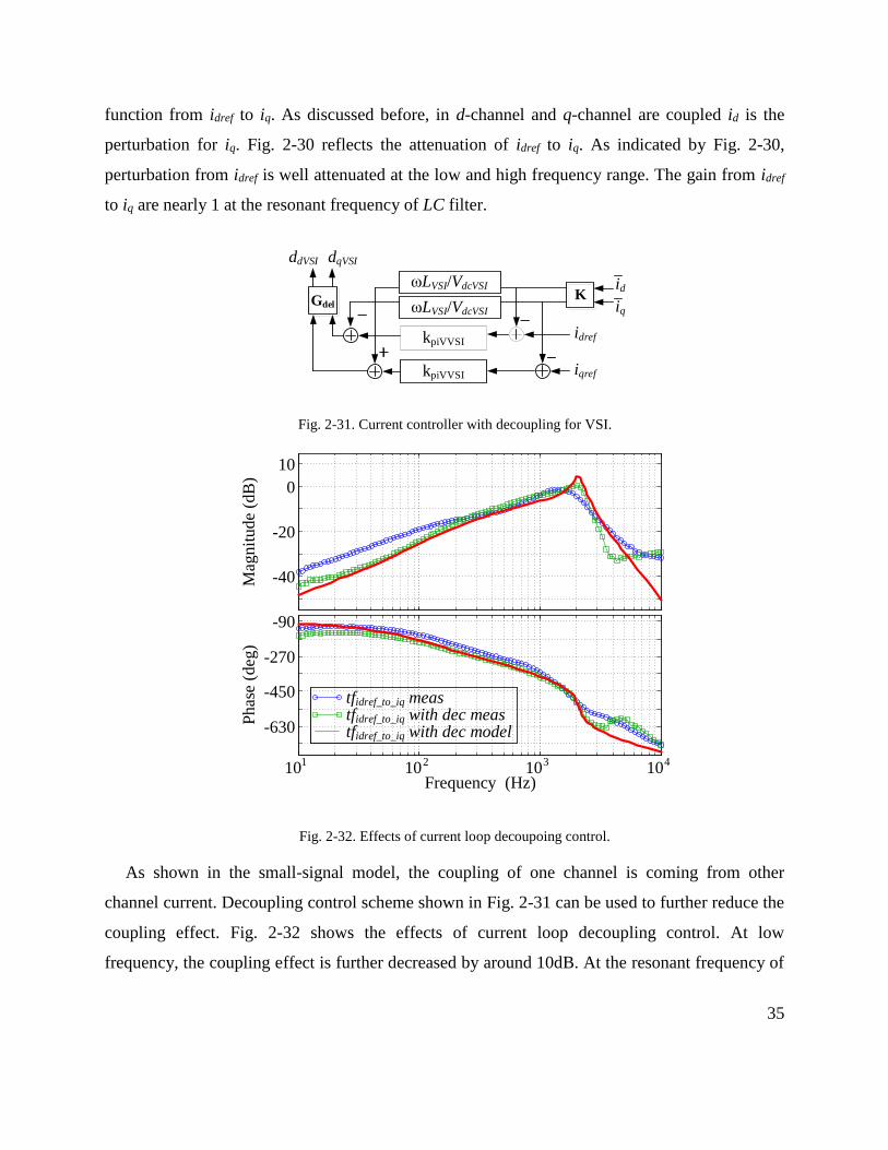
35
function from idref to iq. As discussed before, in d-channel and q-channel are coupled id is the
perturbation for iq. Fig. 2-30 reflects the attenuation of idref to iq. As indicated by Fig. 2-30,
perturbation from idref is well attenuated at the low and high frequency range. The gain from idref
to iq are nearly 1 at the resonant frequency of LC filter.
kpiVVSI
Kiq
id
Gdel
iqref
idref
dqVSIddVSI
ωLVSI/VdcVSI
ωLVSI/VdcVSI
kpiVVSI
Fig. 2-31. Current controller with decoupling for VSI.
Frequency (Hz)10
110
210
410
3
Mag
nit
ude
(dB
)P
has
e (d
eg)
tfidref_to_iq meastfidref_to_iq with dec meastfidref_to_iq with dec model
-40
-20
0
10
-630
-450
-270
-90
Fig. 2-32. Effects of current loop decoupoing control.
As shown in the small-signal model, the coupling of one channel is coming from other
channel current. Decoupling control scheme shown in Fig. 2-31 can be used to further reduce the
coupling effect. Fig. 2-32 shows the effects of current loop decoupling control. At low
frequency, the coupling effect is further decreased by around 10dB. At the resonant frequency of
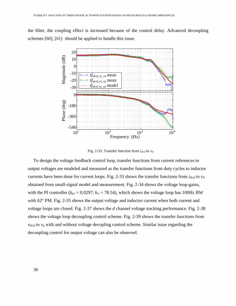
STABILITY ANALYSIS OF THREE-PHASE AC POWER SYSTEMS BASED ON MEASURED D-Q FRAME IMPEDANCES
36
the filter, the coupling effect is increased because of the control delay. Advanced decoupling
schemes [60], [61] should be applied to handle this issue.
Frequency (Hz)10
110
210
410
3
Mag
nit
ude
(dB
)P
has
e (d
eg)
-30
-20
-10
0
10
20
-540
-360
-180
0
tfidref_to_vd meas
tfiqref_to_vq meas
tfidref_to_vd model
Fig. 2-33. Transfer function from idref to vd.
To design the voltage feedback control loop, transfer functions from current references to
output voltages are modeled and measured as the transfer functions from duty cycles to inductor
currents have been done for current loops. Fig. 2-33 shows the transfer functions from idref to vd
obtained from small-signal model and measurement. Fig. 2-34 shows the voltage loop-gains,
with the PI controller (kpv = 0.0297; kiv = 78.54), which shows the voltage loop has 100Hz BW
with 62° PM. Fig. 2-35 shows the output voltage and inductor current when both current and
voltage loops are closed. Fig. 2-37 shows the d channel voltage tracking performance. Fig. 2-38
shows the voltage loop decoupling control scheme. Fig. 2-39 shows the transfer functions from
vdref to vq with and without voltage decopling control scheme. Similar issue regarding the
decoupling control for output voltage can also be observed.
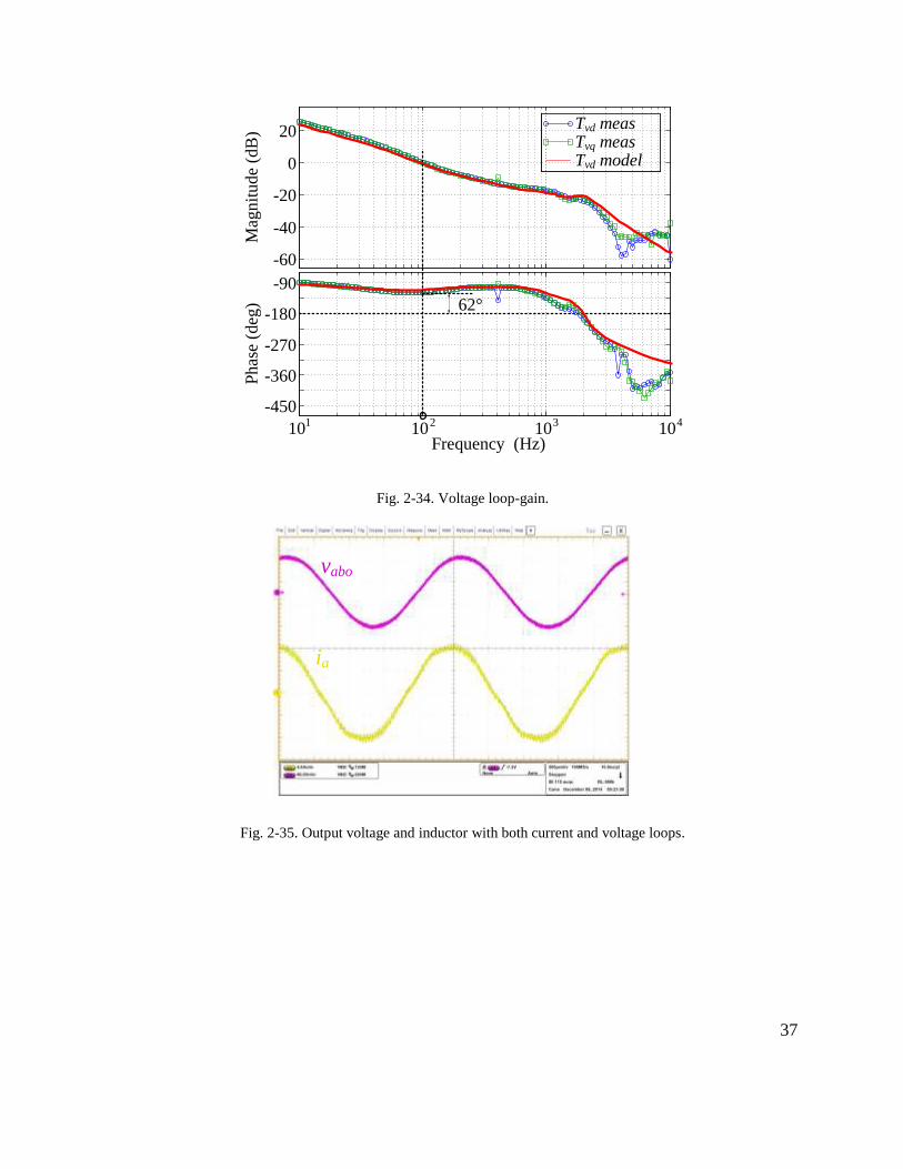
37
Frequency (Hz)10
110
210
410
3
Mag
nit
ude
(dB
)P
has
e (d
eg)
Tvd modelTvq measTvd meas
-60
-40
-20
0
20
-450
-360
-270
-180
-90
62°
Fig. 2-34. Voltage loop-gain.
vabo
ia
Fig. 2-35. Output voltage and inductor with both current and voltage loops.

STABILITY ANALYSIS OF THREE-PHASE AC POWER SYSTEMS BASED ON MEASURED D-Q FRAME IMPEDANCES
38
vabo
ia
vd
vq
Fig. 2-36. Voltage reference step responses with both current and voltage loops.
-60
-40
-20
0
-270
-180
-90
0
Frequency (Hz)10
110
210
410
3
Mag
nit
ude
(dB
)P
has
e (d
eg)
tfvdref_to_vd modeltfvdref_vd meas
Fig. 2-37. Transfer function from vdref to vd.

39
K
Vdref
Vqref
voq
vod
iqref
idref
ωCVSI
ωCVSI
kpvVVSI+kivVVSI/s
kpvVVSI+kivVVSI/s
Fig. 2-38. Voltage controller with decoupling for VSI.
Frequency (Hz)10
110
210
410
3
Mag
nit
ud
e (d
B)
Ph
ase
(deg
)
-80
-60
-40
-20
0
-360
-180
0
180
tfvdref_vq with dec model
tfvdref_to_vq meastfvdref_to_vq with dec meas
Fig. 2-39. Effects of voltage loop decouping control.
2.3 Input and output impedance of VSCs
GNC is an method to predict stability at ac interface using source and load impedances matrix
ratio in the d-q frame. Understanding the input and output impedances of AFE and VSI are
critical for stability analysis of the ac system consist of VSCs.
Small-signal impedance is derived by linearizing the average model around a dc operation
point. By doing d-q transformation, three-phase inverter circuit becomes dc circuit with two
coupled channels as been discussed in last section. The impedance in d-q frame is a 2×2 matrix,
perturbation on output current of one channel produces response from itself and the cross-

STABILITY ANALYSIS OF THREE-PHASE AC POWER SYSTEMS BASED ON MEASURED D-Q FRAME IMPEDANCES
40
coupling channel [41]. Using the small-signal discussed in las section, this section will discuss
the modeling process of output impedance of VSI. The average model of VSI with feedback
control is shown in Fig. 2-40. The modeling process follows the steps of modeling the output
impedance of inverter power stage in d-q frame, the influence of current feedback control, and
the influence of voltage feedback control.
kpi+kii/s kpv+kiv/s
kpv+kiv/skpi+kii/s
K Kiq
id
ZdqVSI
Vdref
Vqref
Gdel
dq
LVSI
iq
LVSI
id
CVSI
RLVSI
RLVSI
dd ωCVSI
CVSI
ωCVSI
vdo
vqo
dqωLVSI id
ωLVSIiq
id iq
vdc
dq vdc
dd vdc
vqo
vdo
vdo
vqo
dd
Fig. 2-40. Average model of VSI in d-q frame with feedback control.
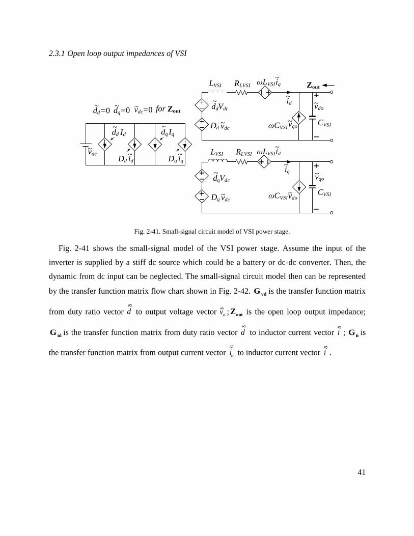
41
2.3.1 Open loop output impedances of VSI
for Zout
id~
iq
~
LVSI RLVSI
LVSI RLVSI
CVSI
CVSI
Vdcdq
~
Dq
~vdc
Iddd
~
Dd id~
Iqdq
~
Dq iq~
~vdc
vdo~
vqo~
Dd~vdc
Vdcdd
~
ωLVSIiq~
ωLVSIid~
ωCVSIvdo~
ωCVSIvqo~
=0dq~
=0~vdc=0dd
~
Zout
Fig. 2-41. Small-signal circuit model of VSI power stage.
Fig. 2-41 shows the small-signal model of the VSI power stage. Assume the input of the
inverter is supplied by a stiff dc source which could be a battery or dc-dc converter. Then, the
dynamic from dc input can be neglected. The small-signal circuit model then can be represented
by the transfer function matrix flow chart shown in Fig. 2-42. vdG is the transfer function matrix
from duty ratio vector d
~
to output voltage vector ov~ ; outZ is the open loop output impedance;
idG is the transfer function matrix from duty ratio vector d
~
to inductor current vector i~
; iiG is
the transfer function matrix from output current vector oi~
to inductor current vector i~
.

STABILITY ANALYSIS OF THREE-PHASE AC POWER SYSTEMS BASED ON MEASURED D-Q FRAME IMPEDANCES
42
+
+
++
Fig. 2-42. VSI power stage small-signal model.
The output impedance can be derived by forcing perturbations of the duty ratio and dc voltage
to zero as shown in Fig. 2-41. The expression of open loop output impedance is:
den
num
den
numden
num
den
num
ZZ
ZZ
qqqd
dqdd
2221
1211
3
1outZ (2-18)
Where,
22232
22222
)33(
)3(
VSILVSIVSIVSI
LVSILVSIVSI
CGLCL
GsCGsCLden
(2-19)
)3(
)3(
2222
2222
11
LVSILVSIVSI
LVSI
GsCGsCL
GLnum
(2-20)
)33(
)3(
2232
2222
12
VSILVSIVSIVSI
LVSI
CGLCL
GLnum
(2-21)
1221 numnum , 1122 numnum (2-22)
LVSIVSIL RsLG 33 (2-23)
Other transfer function matrix can be derived using the same methodology.
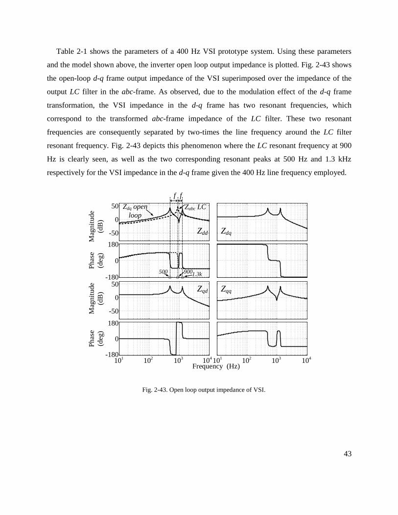
43
Table 2-1 shows the parameters of a 400 Hz VSI prototype system. Using these parameters
and the model shown above, the inverter open loop output impedance is plotted. Fig. 2-43 shows
the open-loop d-q frame output impedance of the VSI superimposed over the impedance of the
output LC filter in the abc-frame. As observed, due to the modulation effect of the d-q frame
transformation, the VSI impedance in the d-q frame has two resonant frequencies, which
correspond to the transformed abc-frame impedance of the LC filter. These two resonant
frequencies are consequently separated by two-times the line frequency around the LC filter
resonant frequency. Fig. 2-43 depicts this phenomenon where the LC resonant frequency at 900
Hz is clearly seen, as well as the two corresponding resonant peaks at 500 Hz and 1.3 kHz
respectively for the VSI impedance in the d-q frame given the 400 Hz line frequency employed.
-50
0
50
-180
0
180
-50
0
50
-180
0
180
101
102
103
101
102
103
104
104
Frequency (Hz)
Mag
nit
ud
e
(dB
)
Ph
ase
(deg
)
Mag
nit
ud
e
(dB
)
Ph
ase
(deg
)
Zabc LCZdq open
loop
f f
900500 1.3k
Zdd Zdq
Zqd Zqq
Fig. 2-43. Open loop output impedance of VSI.
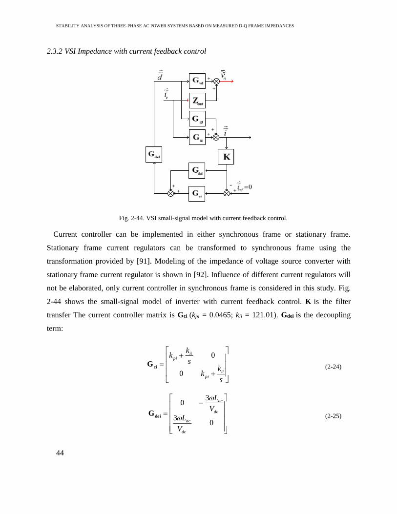
STABILITY ANALYSIS OF THREE-PHASE AC POWER SYSTEMS BASED ON MEASURED D-Q FRAME IMPEDANCES
44
2.3.2 VSI Impedance with current feedback control
+
+
++
++
+-
Fig. 2-44. VSI small-signal model with current feedback control.
Current controller can be implemented in either synchronous frame or stationary frame.
Stationary frame current regulators can be transformed to synchronous frame using the
transformation provided by [91]. Modeling of the impedance of voltage source converter with
stationary frame current regulator is shown in [92]. Influence of different current regulators will
not be elaborated, only current controller in synchronous frame is considered in this study. Fig.
2-44 shows the small-signal model of inverter with current feedback control. K is the filter
transfer The current controller matrix is Gci (kpi = 0.0465; kii = 121.01). Gdei is the decoupling
term:
s
kk
s
kk
iipi
iipi
0
0
ciG (2-24)
03
30
dc
ac
dc
ac
V
L
V
L
deiG (2-25)
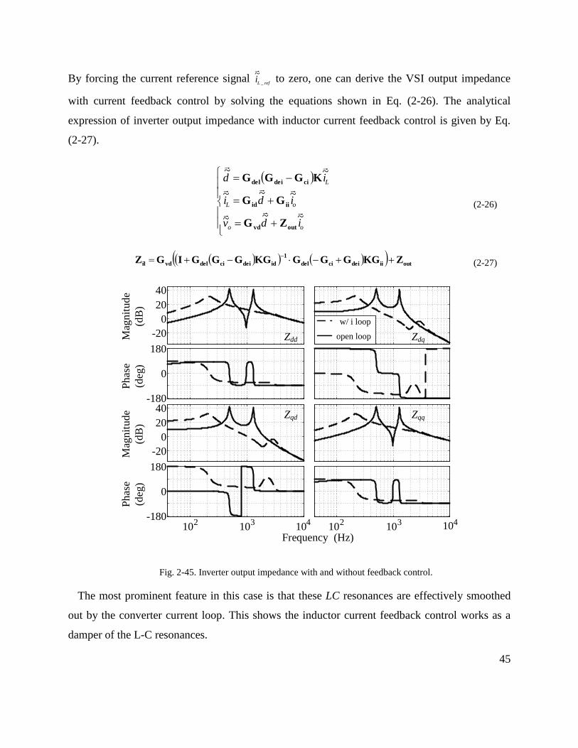
45
By forcing the current reference signal refL
i_
~
to zero, one can derive the VSI output impedance
with current feedback control by solving the equations shown in Eq. (2-26). The analytical
expression of inverter output impedance with inductor current feedback control is given by Eq.
(2-27).
oo
oL
L
idv
idi
id
~~~
~~~
~~
outvd
iiid
cideidel
ZG
GG
KGGG
(2-26)
outiideicidel
1
iddeicidelvdil ZKGGGGKGGGGIGZ (2-27)
-20
0
20
40
-180
0
180
-20
0
20
40
-180
0
180
w/ i loop
open loop
102
103
104
102
103 104
Frequency (Hz)
Mag
nit
ude
(dB
)
Phas
e
(deg
)
Mag
nit
ude
(dB
)
Phas
e
(deg
)
Zdd Zdq
Zqd Zqq
Fig. 2-45. Inverter output impedance with and without feedback control.
The most prominent feature in this case is that these LC resonances are effectively smoothed
out by the converter current loop. This shows the inductor current feedback control works as a
damper of the L-C resonances.
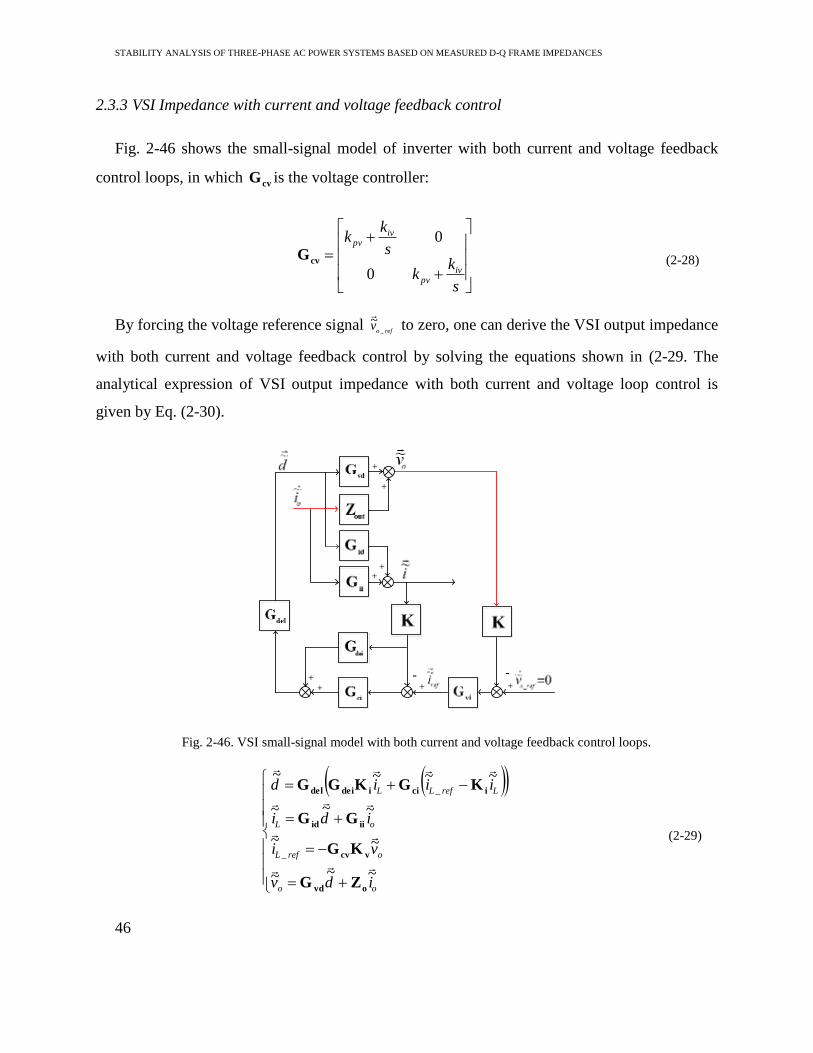
STABILITY ANALYSIS OF THREE-PHASE AC POWER SYSTEMS BASED ON MEASURED D-Q FRAME IMPEDANCES
46
2.3.3 VSI Impedance with current and voltage feedback control
Fig. 2-46 shows the small-signal model of inverter with both current and voltage feedback
control loops, in which cvG is the voltage controller:
s
kk
s
kk
ivpv
ivpv
0
0
cvG (2-28)
By forcing the voltage reference signal refo
v_
~
to zero, one can derive the VSI output impedance
with both current and voltage feedback control by solving the equations shown in (2-29. The
analytical expression of VSI output impedance with both current and voltage loop control is
given by Eq. (2-30).
+
+
++
++
+ +
--
Fig. 2-46. VSI small-signal model with both current and voltage feedback control loops.
oo
orefL
oL
LrefLL
idv
vi
idi
iiid
~~~
~~
~~~
~~~~
_
_
ovd
vcv
iiid
iciideidel
ZG
KG
GG
KGKGG
(2-29)
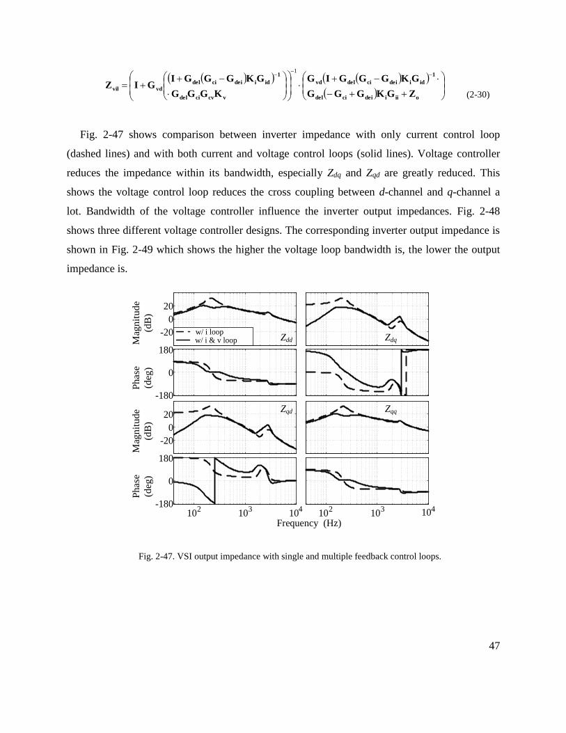
47
oiiideicidel
1
idideicidelvd
vcvcidel
1
idideicidel
vdvilZGKGGG
GKGGGIG
KGGG
GKGGGIGIZ
1
(2-30)
Fig. 2-47 shows comparison between inverter impedance with only current control loop
(dashed lines) and with both current and voltage control loops (solid lines). Voltage controller
reduces the impedance within its bandwidth, especially Zdq and Zqd are greatly reduced. This
shows the voltage control loop reduces the cross coupling between d-channel and q-channel a
lot. Bandwidth of the voltage controller influence the inverter output impedances. Fig. 2-48
shows three different voltage controller designs. The corresponding inverter output impedance is
shown in Fig. 2-49 which shows the higher the voltage loop bandwidth is, the lower the output
impedance is.
-20
0
20
-180
0
180
-20
0
20
-180
0
180
w/ i loopw/ i & v loop
102
103
104
102
103 104
Frequency (Hz)
Mag
nit
ude
(dB
)
Phase
(deg)
Mag
nit
ude
(dB
)
Phase
(deg)
Zdd Zdq
Zqd Zqq
Fig. 2-47. VSI output impedance with single and multiple feedback control loops.
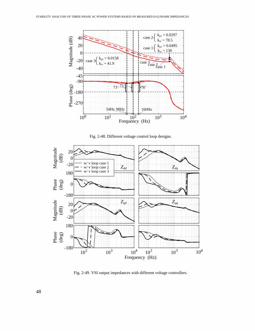
STABILITY ANALYSIS OF THREE-PHASE AC POWER SYSTEMS BASED ON MEASURED D-Q FRAME IMPEDANCES
48
104
-270
-180
-90
-45P
has
e (d
eg)
Frequency (Hz)
-40
-20
0
20
40
Mag
nit
ude
(dB
)
103102101100
54Hz
73°
98Hz
75°
160Hz
78°
case 3case 2
case 1
case 2kpv = 0.0297
kiv = 78.5
case 3kpv = 0.0158
kiv = 41.9
case 1kpv = 0.0495
kiv = 130
Fig. 2-48. Different voltage control loop designs.
-20
0
20
-180
0
180
-20
0
20
-180
0
180
w/ v loop case 1w/ v loop case 2w/ v loop case 3
102
103
104
102
103 104
Mag
nit
ud
e
(dB
)
Ph
ase
(deg
)
Mag
nit
ud
e
(dB
)
Ph
ase
(deg
)
Frequency (Hz)
Zdd Zdq
Zqd Zqq
Fig. 2-49. VSI output impedances with different voltage controllers.

49
2.3.4 AFE input impedances
Same d-q impedances modeling approach discussed for VSI can be used for three-phase AFE.
Fig. 2-50 shows the average model with feedback control. In this model, TΔθ is the d-q
transformation.
cossin
sincosT (2-31)
LAFE
Cdc_AFE
Rdc
ZdqAFE
id dd
vdc_AFE dd
dqvdc_AFE
iqdq
vd
vq
kppll+kipll/s 1/svd
vqK Kω Δθ
-1
kpv+kiv/s Kkpi+kii/s
kpi+kii/s
vdc_AFE
vdc_AFE
IqLref
VdcrefGdel
dd dq
ΔθT
ΔθT
ΔθT
RLAFE
LAFERLAFE
id
ωLAFEiq
iq
ωLAFEid
iq
id
Fig. 2-50. Small-signal model of AFE.

STABILITY ANALYSIS OF THREE-PHASE AC POWER SYSTEMS BASED ON MEASURED D-Q FRAME IMPEDANCES
50
-50
0
50
-180
0
180
-20
0
20
40
-180
0
180
101
102
103
101
102
103
104
104
Frequency (Hz)
Mag
nit
ud
e
(dB
)
Ph
ase
(deg
)
Mag
nit
ud
e
(dB
)
Ph
ase
(deg
)
Zdq open
loop
Zdq control
Zdd Zdq
Zqd Zqq
Fig. 2-51. AFE input impedance in d-q frame.
Fig. 2-51 shows the open-loop (black solid line) and closed-loop (red dash line) d-q frame
input impedance of the VSC. As it can be observed, the open-loop impedance is a combination
of the ac side inductor impedance (at high frequency) and the dc side impedance of capacitor and
resistor (at low frequency) weighted by d channel and q channel duty ratios. After the closed-
loop control (unity power factor control in this paper) is applied, the negative resistor impedance
effect can be observed in the d channel impedance Zdd, which is the main feature of the AFE
input impedance, a direct result of its constant power load dynamics. In this case the higher the
control bandwidth of the AFE voltage loop is, the wider the frequency range of the negative
resistor is.When dc voltage is controlled, with certain load, AFE is a constant power load [39]. In
the feedback control system shown in Fig. 2-50, output of dc voltage control loop gives the
reference of d channel current. Then, dc side power is delivered through d channel from ac side.
Eq. (2-32) reflects this relationship. After small-signal linearization process (Eq. (2-32) to Eq.
(2-34)), Eq. (2-34) shows that dd
Z is a negative incremental resistor.
s
d
s
d
s
d
s
d
s
d
s
d
dc
dcAFE vViIVIR
V ~~2
(2-32)
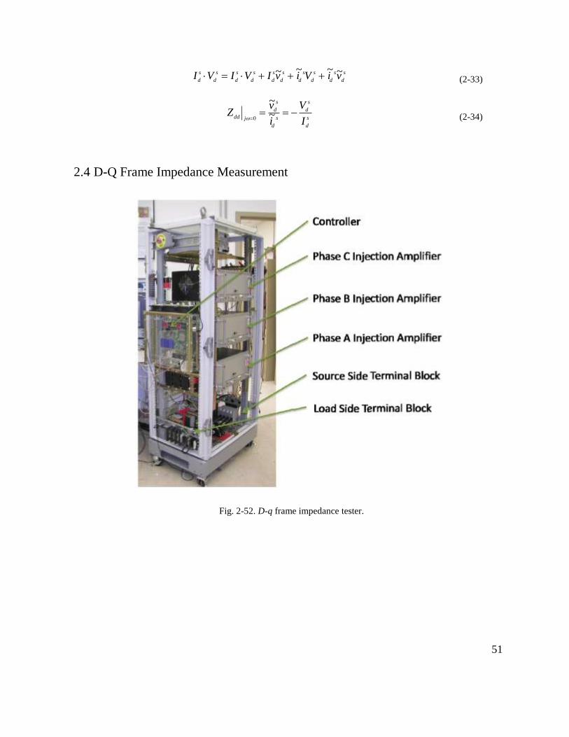
51
s
d
s
d
s
d
s
d
s
d
s
d
s
d
s
d
s
d
s
dviVivIVIVI ~~~~ (2-33)
s
d
s
d
s
d
s
d
jddI
V
i
vZ
~
~
0 (2-34)
2.4 D-Q Frame Impedance Measurement
Fig. 2-52. D-q frame impedance tester.
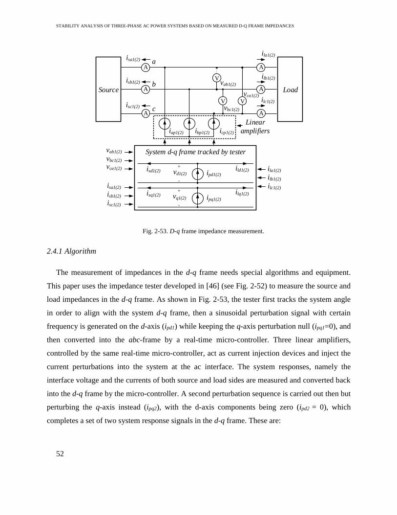
STABILITY ANALYSIS OF THREE-PHASE AC POWER SYSTEMS BASED ON MEASURED D-Q FRAME IMPEDANCES
52
iap1(2) ibp1(2) icp1(2)
ipd1(2)vd1(2)isd1(2) ild1(2)
System d-q frame tracked by tester
V
isc1(2)
ilc1(2)
cA A
isa1(2)
ila1(2)
aA A
isb1(2)ilb1(2)
bA A
+
-
+
-
V V
vab1(2)
vbc1(2)
vca1(2)
isq1(2) vq1(2) ipq1(2)
ilq1(2)
isa1(2)
isb1(2)
isc1(2)
vab1(2)
vbc1(2)
vca1(2) ila1(2)
ilb1(2)
ilc1(2)
Linear
amplifiers
LoadSource
Fig. 2-53. D-q frame impedance measurement.
2.4.1 Algorithm
The measurement of impedances in the d-q frame needs special algorithms and equipment.
This paper uses the impedance tester developed in [46] (see Fig. 2-52) to measure the source and
load impedances in the d-q frame. As shown in Fig. 2-53, the tester first tracks the system angle
in order to align with the system d-q frame, then a sinusoidal perturbation signal with certain
frequency is generated on the d-axis (ipd1) while keeping the q-axis perturbation null (ipq1=0), and
then converted into the abc-frame by a real-time micro-controller. Three linear amplifiers,
controlled by the same real-time micro-controller, act as current injection devices and inject the
current perturbations into the system at the ac interface. The system responses, namely the
interface voltage and the currents of both source and load sides are measured and converted back
into the d-q frame by the micro-controller. A second perturbation sequence is carried out then but
perturbing the q-axis instead (ipq2), with the d-axis components being zero (ipd2 = 0), which
completes a set of two system response signals in the d-q frame. These are:

53
2
2
2
2
2
2
1
1
1
1
1
1,,;,,
sq
sd
lq
ld
q
d
sq
sd
lq
ld
q
d
i
i
i
i
v
v
i
i
i
i
v
v (2-35)
lqqlqd
ldqldd
ZZ
ZZldq
Z (2-36)
sqqsqd
sdqsdd
ZZ
ZZsdq
Z (2-37)
Let the subscripts 1 and 2 denote the variables measured during the two independent
perturbations, and let (2-36) and (2-37) be the definition of the load and source impedance in the
d-q frame. Then when measuring the load impedance Zldq, the two perturbations yield:
1
1
1
1
lq
ld
lqqlqd
ldqldd
q
d
i
i
ZZ
ZZ
v
v (2-38)
2
2
2
2
lq
ld
lqqlqd
ldqldd
q
d
i
i
ZZ
ZZ
v
v (2-39)
Notice that since the system is the same, the impedance must remain unchanged. Then
equations (2-38) and (2-39) containing vd1 and vd2 can be regrouped as in (2-40), and the
equations containing vq1 and vq2 can be regrouped as in (2-41).
ldq
ldd
lqld
lqld
d
d
Z
Z
ii
ii
v
v
22
11
2
1 (2-40)
lqq
lqd
lqld
lqld
q
q
Z
Z
ii
ii
v
v
22
11
2
1
(2-41)
Eq. (2-40) and (2-41) in turn can similarly be regrouped as:
21
21
21
21
lqlq
ldld
lqqlqd
ldqldd
dd
ii
ii
ZZ
ZZ
vv
vv (2-42)
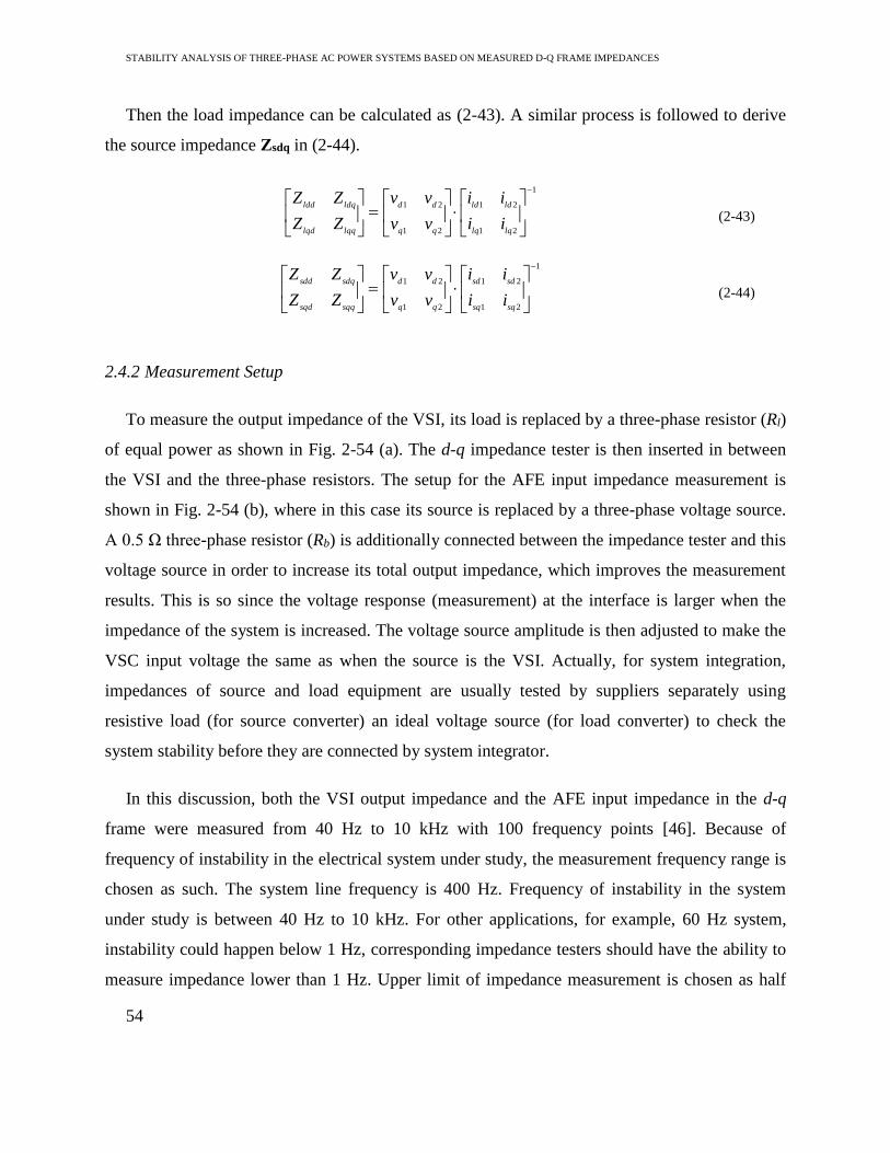
STABILITY ANALYSIS OF THREE-PHASE AC POWER SYSTEMS BASED ON MEASURED D-Q FRAME IMPEDANCES
54
Then the load impedance can be calculated as (2-43). A similar process is followed to derive
the source impedance Zsdq in (2-44).
1
21
21
21
21
lqlq
ldld
dd
lqqlqd
ldqldd
ii
ii
vv
vv
ZZ
ZZ (2-43)
1
21
21
21
21
sqsq
sdsd
dd
sqqsqd
sdqsdd
ii
ii
vv
vv
ZZ
ZZ (2-44)
2.4.2 Measurement Setup
To measure the output impedance of the VSI, its load is replaced by a three-phase resistor (Rl)
of equal power as shown in Fig. 2-54 (a). The d-q impedance tester is then inserted in between
the VSI and the three-phase resistors. The setup for the AFE input impedance measurement is
shown in Fig. 2-54 (b), where in this case its source is replaced by a three-phase voltage source.
A 0.5 Ω three-phase resistor (Rb) is additionally connected between the impedance tester and this
voltage source in order to increase its total output impedance, which improves the measurement
results. This is so since the voltage response (measurement) at the interface is larger when the
impedance of the system is increased. The voltage source amplitude is then adjusted to make the
VSC input voltage the same as when the source is the VSI. Actually, for system integration,
impedances of source and load equipment are usually tested by suppliers separately using
resistive load (for source converter) an ideal voltage source (for load converter) to check the
system stability before they are connected by system integrator.
In this discussion, both the VSI output impedance and the AFE input impedance in the d-q
frame were measured from 40 Hz to 10 kHz with 100 frequency points [46]. Because of
frequency of instability in the electrical system under study, the measurement frequency range is
chosen as such. The system line frequency is 400 Hz. Frequency of instability in the system
under study is between 40 Hz to 10 kHz. For other applications, for example, 60 Hz system,
instability could happen below 1 Hz, corresponding impedance testers should have the ability to
measure impedance lower than 1 Hz. Upper limit of impedance measurement is chosen as half
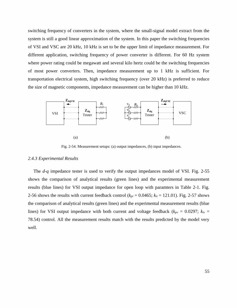
55
switching frequency of converters in the system, where the small-signal model extract from the
system is still a good linear approximation of the system. In this paper the switching frequencies
of VSI and VSC are 20 kHz, 10 kHz is set to be the upper limit of impedance measurement. For
different application, switching frequency of power converter is different. For 60 Hz system
where power rating could be megawatt and several kilo hertz could be the switching frequencies
of most power converters. Then, impedance measurement up to 1 kHz is sufficient. For
transportation electrical system, high switching frequency (over 20 kHz) is preferred to reduce
the size of magnetic components, impedance measurement can be higher than 10 kHz.
ZdqVSI
Zdq
Tester
Rl
VSI
ZdqVSC
Zdq
Tester
Rbva
vb
vcVSC
(a) (b)
Fig. 2-54. Measurement setups: (a) output impedances, (b) input impedances.
2.4.3 Experimental Results
The d-q impedance tester is used to verify the output impedances model of VSI. Fig. 2-55
shows the comparison of analytical results (green lines) and the experimental measurement
results (blue lines) for VSI output impedance for open loop with paramters in Table 2-1. Fig.
2-56 shows the results with current feedback control (kpi = 0.0465; kii = 121.01). Fig. 2-57 shows
the comparison of analytical results (green lines) and the experimental measurement results (blue
lines) for VSI output impedance with both current and voltage feedback (kpv = 0.0297; kiv =
78.54) control. All the measurement results match with the results predicted by the model very
well.
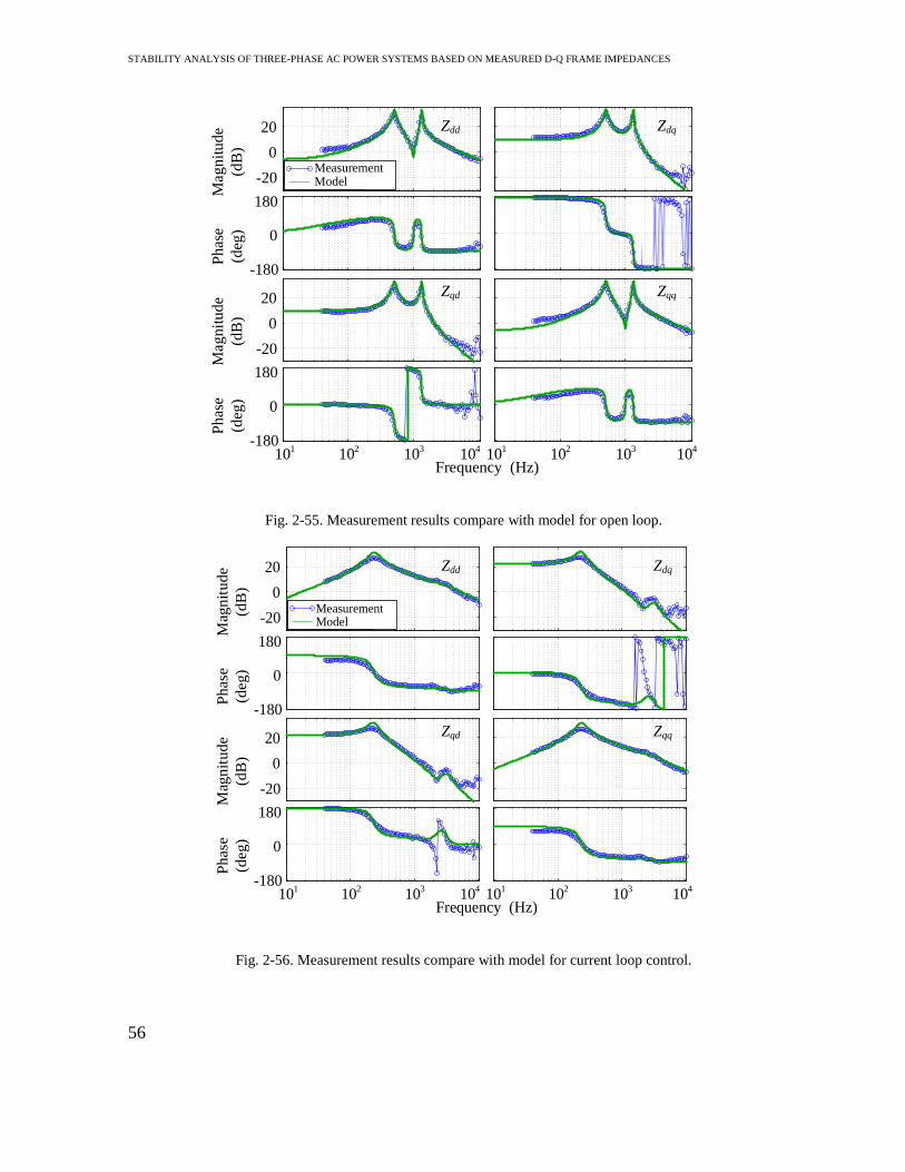
STABILITY ANALYSIS OF THREE-PHASE AC POWER SYSTEMS BASED ON MEASURED D-Q FRAME IMPEDANCES
56
-20
0
20
-20
0
20
Measurement Model
-180
0
180
-180
0
180
Frequency (Hz)
Mag
nit
ud
e
(dB
)
Ph
ase
(deg
)
Mag
nit
ud
e
(dB
)
Ph
ase
(deg
)
101
102
103
104
Zdd
Zqd
101
102
103
104
Zdq
Zqq
Fig. 2-55. Measurement results compare with model for open loop.
MeasurementModel-20
0
20
-20
0
20
-180
0
180
-180
0
180
Frequency (Hz)
Mag
nit
ud
e
(dB
)
Ph
ase
(deg)
Mag
nit
ud
e
(dB
)
Ph
ase
(deg)
101
102
103
104
Zdd
Zqd
101
102
103
104
Zdq
Zqq
Fig. 2-56. Measurement results compare with model for current loop control.
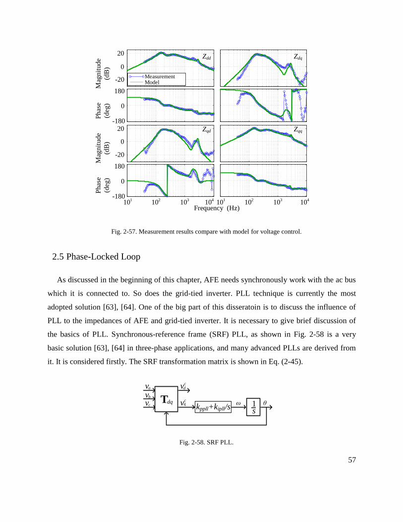
57
MeasurementModel-20
0
20
-20
0
20-180
0
180
-180
0
180
Frequency (Hz)
Mag
nit
ude
(dB
)
Phas
e
(deg
)
Mag
nit
ude
(dB
)
Phas
e
(deg
)
101
102
103
104
Zdd
Zqd
101
102
103
104
Zdq
Zqq
Fig. 2-57. Measurement results compare with model for voltage control.
2.5 Phase-Locked Loop
As discussed in the beginning of this chapter, AFE needs synchronously work with the ac bus
which it is connected to. So does the grid-tied inverter. PLL technique is currently the most
adopted solution [63], [64]. One of the big part of this disseratoin is to discuss the influence of
PLL to the impedances of AFE and grid-tied inverter. It is necessary to give brief discussion of
the basics of PLL. Synchronous-reference frame (SRF) PLL, as shown in Fig. 2-58 is a very
basic solution [63], [64] in three-phase applications, and many advanced PLLs are derived from
it. It is considered firstly. The SRF transformation matrix is shown in Eq. (2-45).
θω
vc
va
vb
1s
vdc
vqcTdq
kppll+kipll/s
Fig. 2-58. SRF PLL.
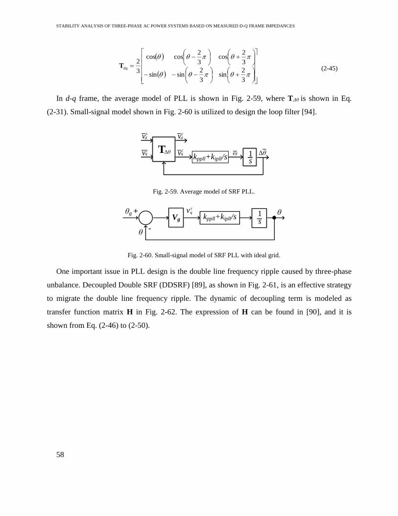
STABILITY ANALYSIS OF THREE-PHASE AC POWER SYSTEMS BASED ON MEASURED D-Q FRAME IMPEDANCES
58
3
2sin
3
2sinsin
3
2cos
3
2coscos
3
2dqT
(2-45)
In d-q frame, the average model of PLL is shown in Fig. 2-59, where TΔθ is shown in Eq.
(2-31). Small-signal model shown in Fig. 2-60 is utilized to design the loop filter [94].
1s
vdc
vqc
kppll+kipll/s
vds
vqs
Δθ ω
TΔθ
Fig. 2-59. Average model of SRF PLL.
θ
θg +
-
θ kppll+kipll/sVg
1s
vqc
Fig. 2-60. Small-signal model of SRF PLL with ideal grid.
One important issue in PLL design is the double line frequency ripple caused by three-phase
unbalance. Decoupled Double SRF (DDSRF) [89], as shown in Fig. 2-61, is an effective strategy
to migrate the double line frequency ripple. The dynamic of decoupling term is modeled as
transfer function matrix H in Fig. 2-62. The expression of H can be found in [90], and it is
shown from Eq. (2-46) to (2-50).
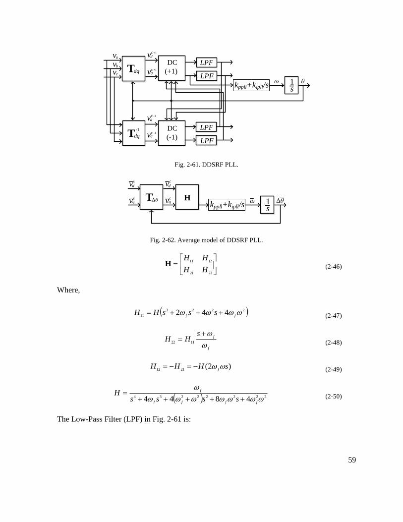
59
-1 DC
(-1)
LPF
LPF
LPF
LPF
DC
(+1)
θω
1s
kppll+kipll/s
va
vb
vcTdq
Tdq
+1vdc
vqc+1
-1vdc
vqc -1
Fig. 2-61. DDSRF PLL.
1s
vdc
vqc
kppll+kipll/s
vds
vqs
Δθ ω
TΔθ H
Fig. 2-62. Average model of DDSRF PLL.
2221
1211
HH
HHH (2-46)
Where,
2223
11442
ffsssHH (2-47)
f
fs
HH
1122
(2-48)
)2(2112
sHHHf (2-49)
22222234 4844
ffff
f
ssssH
(2-50)
The Low-Pass Filter (LPF) in Fig. 2-61 is:

STABILITY ANALYSIS OF THREE-PHASE AC POWER SYSTEMS BASED ON MEASURED D-Q FRAME IMPEDANCES
60
f
f
sLPF
(2-51)

61
Chapter 3 Small-signal Stability in the Presence of Constant
Power Load
3.1 Introduction
This chapter presents, for the first time, the small-signal stability analysis of a balanced three-
phase ac system with constant power loads based on the GNC and measured impedances in d-q
frame. To this end, three experiments are shown for stable, critical stable, and unstable
conditions, demonstrating the stability prediction accuracy of the approach. Furthermore, results
in the time and frequency domains are put side-by-side to show the effectiveness of the stability
analysis based on the measured impedances. This also validates the assumptions previously
made to study the stability of ac systems using the GNC and simulation-based analysis.
Specifically, using the d-q impedance measurement algorithm and equipment developed in [46],
this paper studies the small-signal stability of an ac system comprised of a voltage source
inverter (VSI) feeding a boost rectifier or voltage source converter (VSC) in this chapter, in what
is regarded a very generic system configuration. In effect, it could represent many applications,
for example, an uninterruptable power supply feeding an active load in a building, or an ac
subsystem within a microgrid as shown in Fig. 3-1. Accordingly, the analysis presented is kept as
generic as possible to be representative of any such ac system interface. Stable and unstable
conditions then are created by adjusting the voltage control bandwidth of the VSI, where by
measuring the source (VSI) output impedance and the load (VSC) input impedance the GNC is
applied characterizing the stability conditions at the ac interface.
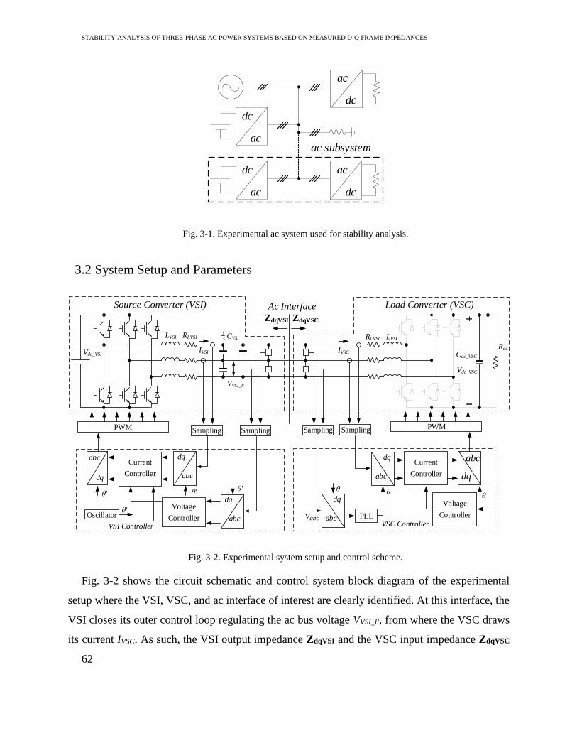
STABILITY ANALYSIS OF THREE-PHASE AC POWER SYSTEMS BASED ON MEASURED D-Q FRAME IMPEDANCES
62
ac
dc
dc
ac
ac
dc
dc
ac
ac subsystem
Fig. 3-1. Experimental ac system used for stability analysis.
3.2 System Setup and Parameters
Source Converter (VSI) Load Converter (VSC)
abc
dq
dq
abc
PWM
VSI Controller
Sampling SamplingPWM
VSC ControllerPLLvabc
SamplingSampling
abc
dqVoltage
Controller
Current
Controller
abc
dq
abc
dq
Voltage
ControllerOscillator
Current
Controller
LVSCRLVSCLVSI RLVSI
Vdc_VSI
Rdc
Cdc_VSC
VVSI_ll
θ'
θ'
θ' θ' θ θθ
ZdqVSI ZdqVSC
Vdc_VSC
IVSCIVSI
Ac Interface
abc
dq
CVSI13
Fig. 3-2. Experimental system setup and control scheme.
Fig. 3-2 shows the circuit schematic and control system block diagram of the experimental
setup where the VSI, VSC, and ac interface of interest are clearly identified. At this interface, the
VSI closes its outer control loop regulating the ac bus voltage VVSI_ll, from where the VSC draws
its current IVSC. As such, the VSI output impedance ZdqVSI and the VSC input impedance ZdqVSC

63
seen at this interface are solely of each converter’s parameters and do not depend on each other’s
components and control systems. Also, when performing the measurements this interface is a
common coupling point fully accessible from the exterior of the VSI and VSC cabinets.
The parameters of this system are listed in Table 3-1.
Table 3-1. Experimental system parameters.
Symbol Description Value
Vdc_VSI VSI input dc voltage 270 V
VVSI_ll VSI output line-line rms voltage 99.6 V
f VSI output voltage frequency 400 Hz
LVSI Inductance of VSI output inductor 970 µH
RLVSI Resistance of VSI output inductor self-resistor 120 mΩ
CVSI Capacitance of VSI output capacitor 31.8 µF
LVSC Inductance of VSC boost inductor 470 µH
RLVSC Resistance of VSC boost inductor self-resistor 90 mΩ
Vdc_VSC VSC output dc voltage 270 V
Cdc_VSC Capacitance of VSC output capacitor 100 µF
Rdc Resistance of VSC load resistor 96 Ω
Rl Resistances of resistor load for VSI output impedance test 13 Ω
Rb Resistances of resistor for VSC input impedance test 0.5 Ω
As seen, the control systems of both converters are implemented in the d-q frame. For the
VSI, the inductor currents are measured in the inner current control-loop, and the capacitor
voltages are measured in the outer voltage control-loop. For the VSC, the input terminal voltages
are measured by the Phase-Locked Loop (PLL) in order to estimate the phase of the ac bus
voltage and synchronize the converter operation. The PLL scheme implemented is based on the
positive-sequence d-q frame transformation [64]. The boost inductor currents are measured in the
inner current control-loop, and the output capacitor voltage is measured in the outer voltage
control-loop. All the regulators employed use a Proportional and Integral (PI) structure, and no
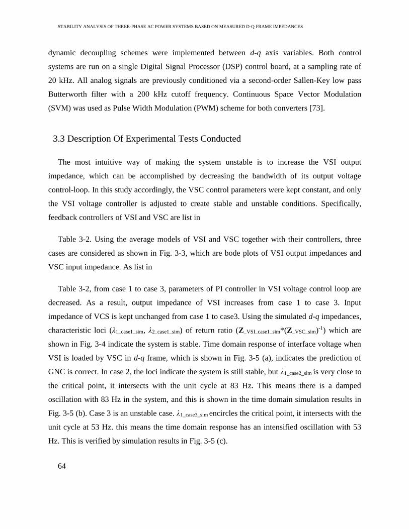
STABILITY ANALYSIS OF THREE-PHASE AC POWER SYSTEMS BASED ON MEASURED D-Q FRAME IMPEDANCES
64
dynamic decoupling schemes were implemented between d-q axis variables. Both control
systems are run on a single Digital Signal Processor (DSP) control board, at a sampling rate of
20 kHz. All analog signals are previously conditioned via a second-order Sallen-Key low pass
Butterworth filter with a 200 kHz cutoff frequency. Continuous Space Vector Modulation
(SVM) was used as Pulse Width Modulation (PWM) scheme for both converters [73].
3.3 Description Of Experimental Tests Conducted
The most intuitive way of making the system unstable is to increase the VSI output
impedance, which can be accomplished by decreasing the bandwidth of its output voltage
control-loop. In this study accordingly, the VSC control parameters were kept constant, and only
the VSI voltage controller is adjusted to create stable and unstable conditions. Specifically,
feedback controllers of VSI and VSC are list in
Table 3-2. Using the average models of VSI and VSC together with their controllers, three
cases are considered as shown in Fig. 3-3, which are bode plots of VSI output impedances and
VSC input impedance. As list in
Table 3-2, from case 1 to case 3, parameters of PI controller in VSI voltage control loop are
decreased. As a result, output impedance of VSI increases from case 1 to case 3. Input
impedance of VCS is kept unchanged from case 1 to case3. Using the simulated d-q impedances,
characteristic loci (λ1_case1_sim, λ2_case1_sim) of return ratio (Z_VSI_case1_sim*(Z_VSC_sim)-1) which are
shown in Fig. 3-4 indicate the system is stable. Time domain response of interface voltage when
VSI is loaded by VSC in d-q frame, which is shown in Fig. 3-5 (a), indicates the prediction of
GNC is correct. In case 2, the loci indicate the system is still stable, but λ1_case2_sim is very close to
the critical point, it intersects with the unit cycle at 83 Hz. This means there is a damped
oscillation with 83 Hz in the system, and this is shown in the time domain simulation results in
Fig. 3-5 (b). Case 3 is an unstable case. λ1_case3_sim encircles the critical point, it intersects with the
unit cycle at 53 Hz. this means the time domain response has an intensified oscillation with 53
Hz. This is verified by simulation results in Fig. 3-5 (c).

65
Table 3-2. Feedback controller parameters for VSI and VSC.
VSI VSC
Voltage loop Current loop Voltage loop Current loop
Case 1 0.0495 + 130/s
0.0465 + 121/s
0.0462 + 4.58/s
0.0116 + 46.5/s Case 2 0.0297 + 78.5/s
Case 3 0.0158 + 41.9/s
-20
0
20
-180
0
180
-20
0
20
-180
0
180
Z_VSC_simZ_VSI_case1_simZ_VSI_case2_simZ_VSI_case3_sim
102
103
104
102
103 104
Mag
nit
ud
e
(dB
)
Ph
ase
(deg
)
Mag
nit
ud
e
(dB
)
Ph
ase
(deg
)
Frequency (Hz)
Zdd Zdq
Zqd Zqq
Fig. 3-3. Impedances of VSI and VSC for three cases from average model simulation.
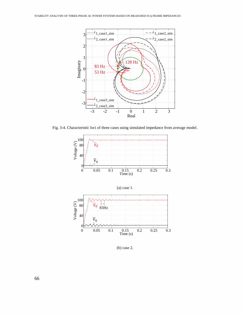
STABILITY ANALYSIS OF THREE-PHASE AC POWER SYSTEMS BASED ON MEASURED D-Q FRAME IMPEDANCES
66
1_case1_sim
2_case1_sim
1_case2_sim
2_case2_sim
1_case3_sim
2_case3_sim
-3 -2 -1 0 1 2 3
-3
-2
-1
0
1
2
3
Real
Imag
inar
y 128 Hz83 Hz
53 Hz
Fig. 3-4. Characteristic loci of three cases using simulated impedance from average model.
0 0.05 0.1 0.15 0.2 0.25 0.3
0
40
80
100
Time (s)
Volt
age
(V)
vq
vd
(a) case 1.
0 0.05 0.1 0.15 0.2 0.25 0.3
0
40
80
100
Time (s)
Volt
age
(V)
83Hz
vq
vd
(b) case 2.
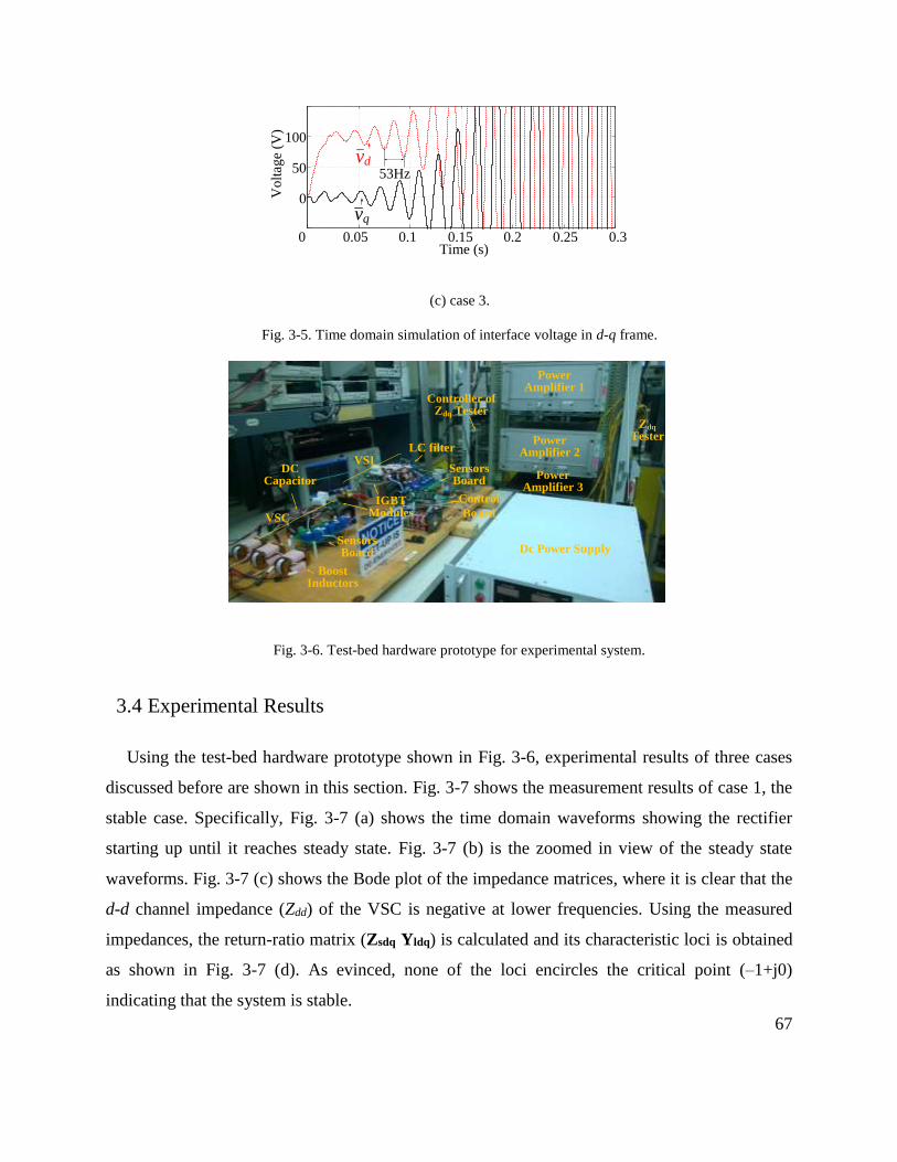
67
0
50
100
0 0.05 0.1 0.15 0.2 0.25 0.3Time (s)
Vo
ltag
e (V
)
53Hz
vq
vd
(c) case 3.
Fig. 3-5. Time domain simulation of interface voltage in d-q frame.
Dc Power Supply
VSI
VSC
Zdq
Tester
Power Amplifier 1
Power Amplifier 2
Power Amplifier 3
Controller of Zdq Tester
Control
Board
LC filter
Sensors Board
IGBT Modules
Sensors Board
Boost Inductors
DC Capacitor
Fig. 3-6. Test-bed hardware prototype for experimental system.
3.4 Experimental Results
Using the test-bed hardware prototype shown in Fig. 3-6, experimental results of three cases
discussed before are shown in this section. Fig. 3-7 shows the measurement results of case 1, the
stable case. Specifically, Fig. 3-7 (a) shows the time domain waveforms showing the rectifier
starting up until it reaches steady state. Fig. 3-7 (b) is the zoomed in view of the steady state
waveforms. Fig. 3-7 (c) shows the Bode plot of the impedance matrices, where it is clear that the
d-d channel impedance (Zdd) of the VSC is negative at lower frequencies. Using the measured
impedances, the return-ratio matrix (Zsdq Yldq) is calculated and its characteristic loci is obtained
as shown in Fig. 3-7 (d). As evinced, none of the loci encircles the critical point (–1+j0)
indicating that the system is stable.
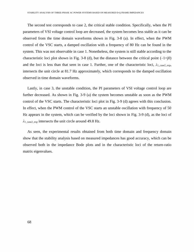
STABILITY ANALYSIS OF THREE-PHASE AC POWER SYSTEMS BASED ON MEASURED D-Q FRAME IMPEDANCES
68
The second test corresponds to case 2, the critical stable condition. Specifically, when the PI
parameters of VSI voltage control loop are decreased, the system becomes less stable as it can be
observed from the time domain waveforms shown in Fig. 3-8 (a). In effect, when the PWM
control of the VSC starts, a damped oscillation with a frequency of 80 Hz can be found in the
system. This was not observable in case 1. Nonetheless, the system is still stable according to the
characteristic loci plot shown in Fig. 3-8 (d), but the distance between the critical point (–1+j0)
and the loci is less than that seen in case 1. Further, one of the characteristic loci, λ1_case2_exp,
intersects the unit circle at 81.7 Hz approximately, which corresponds to the damped oscillation
observed in time domain waveforms.
Lastly, in case 3, the unstable condition, the PI parameters of VSI voltage control loop are
further decreased. As shown in Fig. 3-9 (a) the system becomes unstable as soon as the PWM
control of the VSC starts. The characteristic loci plot in Fig. 3-9 (d) agrees with this conclusion.
In effect, when the PWM control of the VSC starts an unstable oscillation with frequency of 50
Hz appears in the system, which can be verified by the loci shown in Fig. 3-9 (d), as the loci of
λ1_case2_exp intersects the unit circle around 49.8 Hz.
As seen, the experimental results obtained from both time domain and frequency domain
show that the stability analysis based on measured impedances has good accuracy, which can be
observed both in the impedance Bode plots and in the characteristic loci of the return-ratio
matrix eigenvalues.

69
Vdc_VSC
Ia_VSC
VVSI_ab
Diode rectification PWM rectification
50ms/div
(a) Time domain results.
Interface a to b voltage (VVSI_ab) (purple) [100 V/div], VSC phase a current (Ia_VSC) (yellow) [6 A/div], VSC
output voltage (Vdc_VSC) (green) [90 V/div]
Vdc_VSCIa_VSC
VVSI_ab2.5ms/div
(b) Zoomed in time domain results.
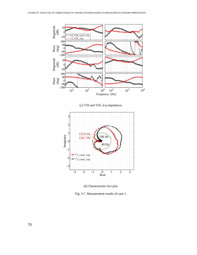
STABILITY ANALYSIS OF THREE-PHASE AC POWER SYSTEMS BASED ON MEASURED D-Q FRAME IMPEDANCES
70
Z_VSI_case1_exp
Z_VSC_exp-20
0
20
-180-90
090
180
-20
0
20
-180-90
090
180
Frequency (Hz)
102
103
104
102
103 104
Mag
nit
ud
e
(dB
)
Ph
ase
(deg
)
Mag
nit
ud
e
(dB
)
Ph
ase
(deg
)
(c) VSI and VSC d-q impedance.
-3 -2 -1 0 1 2 3
-3
-2
-1
0
1
2
3
133.8 Hz
126.7 Hz
40 Hz
10k Hz
Real
Imag
inar
y
1_case1_exp
2_case1_exp
(d) Characteristic loci plot.
Fig. 3-7. Measurement results of case 1.

71
Vdc_VSC
Ia_VSC
VVSI_ab
Diode rectification PWM rectification
50ms/div
80Hz
(a) Time domain results.
Interface a to b voltage (VVSI_ab) (purple) [100 V/div], VSC phase a current (Ia_VSC) (yellow) [6 A/div], VSC
output voltage (Vdc_VSC) (green) [90 V/div]
Vdc_VSCIa_VSC
VVSI_ab
5ms/div
(b) Zoomed in time domain results.
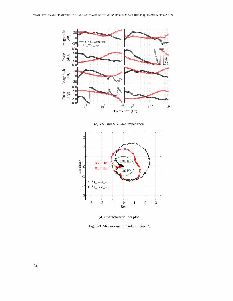
STABILITY ANALYSIS OF THREE-PHASE AC POWER SYSTEMS BASED ON MEASURED D-Q FRAME IMPEDANCES
72
Z_VSI_case2_exp
Z_VSC_exp-20
0
20
-180-90
090
180
-20
0
20
-180-90
090
180
Frequency (Hz)
102
103
104
102
103 104
Mag
nit
ude
(dB
)
Phas
e
(deg
)
Mag
nit
ude
(dB
)
Phas
e
(deg
)
(c) VSI and VSC d-q impedance.
86.3 Hz
81.7 Hz40 Hz
10k Hz
-3 -2 -1 0 1 2 3
-3
-2
-1
0
1
2
3
Real
Imag
inar
y
1_case2_exp
2_case2_exp
(d) Characteristic loci plot.
Fig. 3-8. Measurement results of case 2.
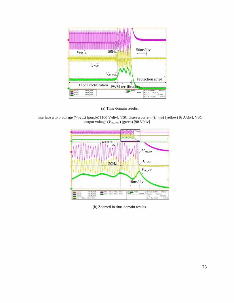
73
Vdc_VSC
Ia_VSC
VVSI_ab
50ms/div50Hz
Diode rectification PWM rectification
Protection acted
(a) Time domain results.
Interface a to b voltage (VVSI_ab) (purple) [100 V/div], VSC phase a current (Ia_VSC) (yellow) [6 A/div], VSC
output voltage (Vdc_VSC) (green) [90 V/div]
Vdc_VSC
Ia_VSC
VVSI_ab
400Hz
50Hz
10ms/div
(b) Zoomed in time domain results.

STABILITY ANALYSIS OF THREE-PHASE AC POWER SYSTEMS BASED ON MEASURED D-Q FRAME IMPEDANCES
74
Z_VSI_case3_exp
Z_VSC_exp-20
0
20
-180-90
090
180
-20
0
20
-180-90
090
180
Frequency (Hz)
102
103
104
102
103 104
Mag
nit
ud
e
(dB
)
Ph
ase
(deg
)
Mag
nit
ud
e
(dB
)
Ph
ase
(deg
)
(c) VSI and VSC d-q impedance.
47.2 Hz
49.8 Hz40 Hz
10k Hz
-3 -2 -1 0 1 2 3
-3
-2
-1
0
1
2
3
Real
Imag
inar
y
1_case3_exp
2_case3_exp
(d) Characteristic loci plot
Fig. 3-9. Measurement results of case 3.
3.5 Discussion
In section 3.3, impedances extracted from average models can predict system stability
accurately in simulation. This is shown by Fig. 3-3 and Fig. 3-4 in frequency domain and

75
verified by Fig. 3-5 in time domain both in d-q frame. These results represent the original theory
of stability analysis using GNC for balanced three-phase ac system. However, it has been
observed that in practice, a lot of uncertainties exit which can influence the robustness of the
analysis. GNC-based small-signal stability analysis for three-phase ac system requires: first, the
three-phase ac system is balanced, second, d-q impedances of the practical system are measured
accurately. Three is no ideal balanced three-phase ac system in practice. On the other hand, d-q
impedance tester relays on PLL to track the system d-q frame and measure impedances. The
accuracy of phase tracking influence the measurement accuracy of impedances and further the
stability analysis.
Unbalance of the experimental system in this paper is kept less than 1%. PLL bandwidth of d-
q impedance tester utilized in this paper is 1 Hz to assure a good phase tracking accuracy. Under
such condition, stability prediction using GNC in experiments shows very good accuracy for the
system under study. Still the paper does not study the robustness of the stability analysis using
GNC, it is an important topic to be explored in the future.
When comparing the simulation results with experimental results, it can be found that,
although they give same conclusion on the stability condition of the system under study, the
oscillation frequencies of the system are different in the two studies. When comparing
impedances of the system in high frequency, there are more differences between simulation and
experimental results. In order to achieve such agreement between simulation and experimental
results, a lot of model verification and validation work have been done. Model validation needs
measurement of from real hardware. This paper presents for the first time, the small-signal
stability analysis of three-phase ac system in the presence of constant power loads based on
measured d-q frame impedances. This work not only demonstrates the feasibility of using GNC
in practice, but also opens the door of model validation for stability analysis using GNC in three-
phase ac system.
The experimental results also demonstrate that three-phase PWM rectifiers with output
voltage control are constant power loads, when the source impedance is high, they can make the
system unstable. From the experimental study, simple design guidance can be provided regarding

STABILITY ANALYSIS OF THREE-PHASE AC POWER SYSTEMS BASED ON MEASURED D-Q FRAME IMPEDANCES
76
ac system with controlled PWM rectifiers. First, in order to make the system stable, source
impedance should be kept small. This can be achieved by increasing the voltage control
bandwidth of the source as shown in this paper. Also, reducing the output voltage control
bandwidth of the rectifier could also stabilized the system. Weak output voltage control reduces
the frequency range of constant power load behavior of three-phase PWM rectifier which
consequently stabilizes the system.
Stability analysis using GNC relies on plotting characteristic loci of the system. Characteristic
loci are calculated from impedances of source and load. Stability cannot be judged intuitively
from impedances interaction as what has been done in dc system. Although some initial work has
been reported to simplify stability analysis using GNC for three-phase system [72] under certain
condition, more efforts are needed before simple design guidance can be provided based on
impedances.
77
Chapter 4 Modeling of Voltage Source Converters Including
Phase-locked Loop
4.1 Introduction
As discussed in the previous chapter, grid-tied VSCs need PLL to synchroniously work with
the grid. These VSCs can be broadly divided as grid-tied inverter and acitive front-end (AFE)
rectifeirs.
Grid-tied inverters are the key components which deliver renewable energy to the grid [62],
[74]. They are typically controlled as current sources injecting current to the grid. With the
increasing penetration of renewable energy resources, power quality and stability issues induced
by grid-tied inverters becomes more and more important [75]–[79]. Harmonic pollution could
happen due to the interaction between inverter and grid impedance [75], [77], [79]. Large grid
impedance could destabilize the inverter system [66], [76]. In order to deliver power to the grid,
frequency and phase angle of inverter output current should synchronize with grid voltage which
is usually served by PLL [63], [64]. Some recent literatures discovered that PLL has negative
impact to the system stability [66], [80]–[84].
Both harmonic and stability issue can be studied using inverter small-signal impedance.
Small-signal impedances of power converters are the linearization around their dc operation
points. For three-phase ac system, no dc operation point exits in stationary frame. By doing
transformation from stationary frame to synchronous reference (d-q) frame, three-phase ac
system becomes two coupled dc system. Small-signal impedances in d-q frame can then be
derived by doing traditional linearization [66], [39], [41], [81]. Different from impedances of dc-
dc converters, impedances of three-phase ac converters are 2-by-2 matrices. Measurement
techniques and devices for d-q frame impedances are also developed [44]–[48]. Small-signal
stability of three-phase ac system can then be analysis based on d-q impedances and generalized
Nyquist Criterion. Recently, small-signal impedances and stability analysis of three-phase
converters are also developed in stationary frame using harmonic linearization on ac signals [67],

STABILITY ANALYSIS OF THREE-PHASE AC POWER SYSTEMS BASED ON MEASURED D-Q FRAME IMPEDANCES
78
[77], [71], [82]. This paper focuses on the traditional d-q impedance analysis in synchronous
reference frame.
D-q small-signal impedance analysis of three-phase grid-tied converters have been reported
for rectifiers without considering the effect of PLL [41], [39]. Ref. [66] models the effect of PLL
by introducing system and converter d-q frames. It shows that high bandwidth PLL increases the
negative real part of inverter output impedance which could destabilize the system [66], [67].
Ref. [81] models the influence of PLL on the input impedance of three-phase boost rectifier. Ref.
[81] gives the full impedance model of grid-tied inverter considering current feedback control
and PLL in d-q frame. The model shows that PLL shapes q-q channel output impedance of grid-
tied inverter as a negative resistor within its bandwidth. Later on, Ref. [85] also shows the same
conclusion using model which ignores the coupling effect between d-channel and q-channel.
This model predicts the inverter impedances well for unity power factor application where
coupling effect can be ignored. However, for three-phase system with reactive power, coupling
effect between d and q channels is significant, this model cannot predict the impedance under
this condition.
abc
dq
dq
abc
PWM
vabc
iabc
Sampling Sampling
Current
Controller
L RL
Vdc
θ
PLL
id
iq
Power
Controller
θ vd vq
idref iqrefθ
Power
Cal.
idiqvdvq
P
Q
Pref
Qref
va
vb
vc
Power Stage
Controller
Fig. 4-1. Grid-tied inverter with feedback control and PLL.
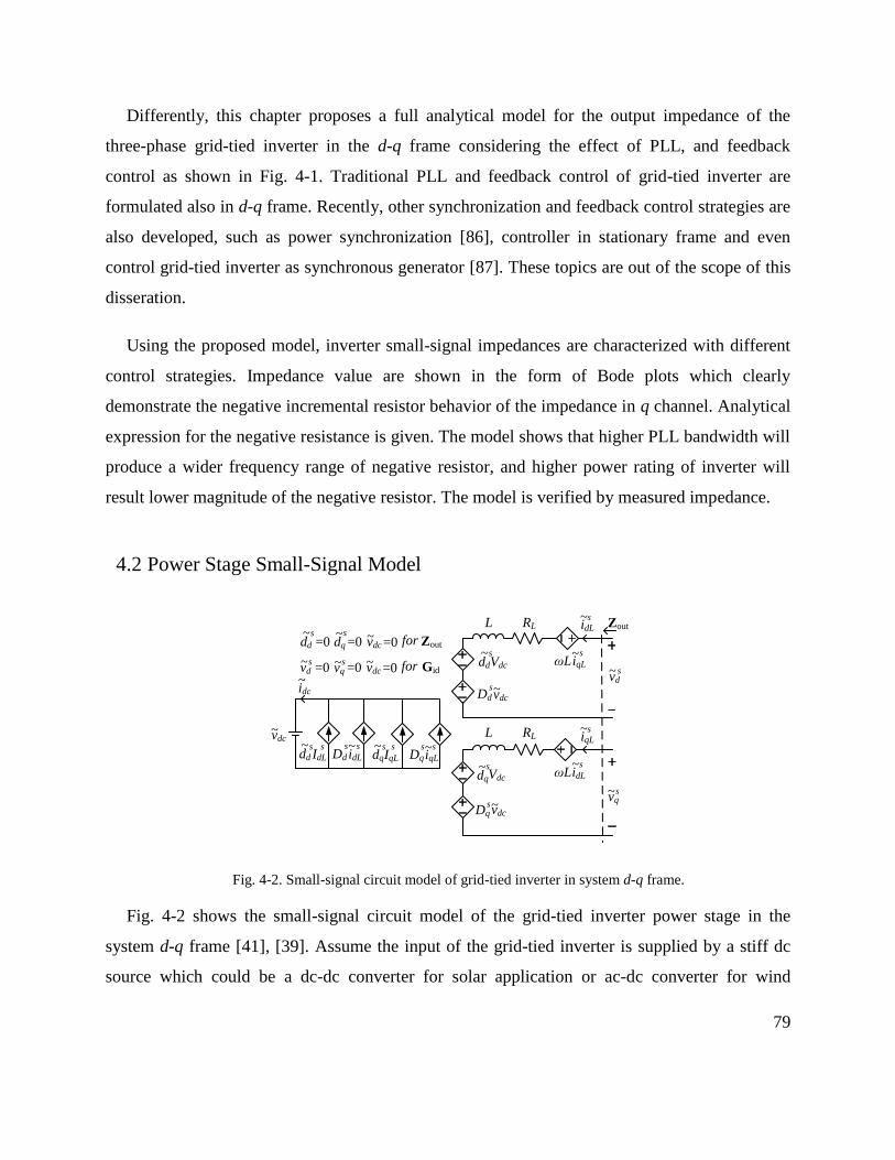
79
Differently, this chapter proposes a full analytical model for the output impedance of the
three-phase grid-tied inverter in the d-q frame considering the effect of PLL, and feedback
control as shown in Fig. 4-1. Traditional PLL and feedback control of grid-tied inverter are
formulated also in d-q frame. Recently, other synchronization and feedback control strategies are
also developed, such as power synchronization [86], controller in stationary frame and even
control grid-tied inverter as synchronous generator [87]. These topics are out of the scope of this
disseration.
Using the proposed model, inverter small-signal impedances are characterized with different
control strategies. Impedance value are shown in the form of Bode plots which clearly
demonstrate the negative incremental resistor behavior of the impedance in q channel. Analytical
expression for the negative resistance is given. The model shows that higher PLL bandwidth will
produce a wider frequency range of negative resistor, and higher power rating of inverter will
result lower magnitude of the negative resistor. The model is verified by measured impedance.
4.2 Power Stage Small-Signal Model
L
idc~
RL
dq
~sIqL
sDq
siqL~s
Dqsvdc~
dqVdc~s
ddVdc
~s
Dd vdc~s
ωLiqL~s
ωLidL~s
iqL~s
vq~s
vd~ s
Zout
vdc~ =0dq
~s=0dd
~s=0 Zoutfor
~vdc~
Dd
sidL
s~IdL
sdd
s
L RL
idL~s
vdc~ =0 Gidforvd
~s=0 vq
~s=0
Fig. 4-2. Small-signal circuit model of grid-tied inverter in system d-q frame.
Fig. 4-2 shows the small-signal circuit model of the grid-tied inverter power stage in the
system d-q frame [41], [39]. Assume the input of the grid-tied inverter is supplied by a stiff dc
source which could be a dc-dc converter for solar application or ac-dc converter for wind

STABILITY ANALYSIS OF THREE-PHASE AC POWER SYSTEMS BASED ON MEASURED D-Q FRAME IMPEDANCES
80
application. Then, the dynamic from dc input can be neglected. The small-signal circuit model
then can be represented by the transfer function matrix flow chart shown in Fig. 4-3. id
G is the
transfer function matrix from duty ratio vector sd
~
to inductor current vector s
Li~
,out
Z is the
output impedance of power stage.
+
+
Fig. 4-3. Power stage small-signal model.
The output impedance can be derived by forcing perturbations of the duty ratio and dc voltage
to zero as shown in Fig. 4-3. The expression of power stage output impedance is:
L
L
qqqd
dqdd
RLsL
LRLs
ZZ
ZZ
out
Z (4-1)
Notice that, impedance of three-phase converter in d-q frame is a 2-by-2 matrix. Zdd
represents the voltage response in d channel when d channel current is perturbed. Zqq represents
the q channel voltage response when q channel current is perturbed. Eq. (4-1) shows that Zdd and
Zqq are the same as the impedance of inverter ac inductor. Zdq and Zqd represent the coupling
effect between d and q channel.
Transfer function matrix between duty ratio vector and inductor current vector can be derived
by forcing perturbations of grid and dc voltage to zero as shown in Fig. 3-2. The expression of
idG is:
L
L
L
dc
RLsL
LRLs
LRLs
V
22id
G (4-2)

81
4.3 Influence of PLL
Output impedance of dc-dc converter is influenced by its power stage parameters and
feedback controller [29]. Different from dc-dc converter, grid-tied converter usually needs PLL
to synchronize with the grid [64]. Because of PLL, the inverter system has two d-q frames, one is
system d-q frame, and another is the controller d-q frame [66] as shown in Fig. 4-4. Grid voltage
defines the system d-q frame. Controller d-q frame is defined by the PLL, which estimates the
frequency and angle of grid voltage to find the position of system d-q frame. In steady state,
controller d-q frame is aligned with the system d-q frame. When small-signal perturbations are
added to the grid voltage, the position of system d-q frame is changed. The controller d-q frame
is no longer aligned with system d-q frame because of the PLL dynamics (PI regulator of PLL).
The angle between two d-q frames is as shown in Fig. 4-4. Voltage and current vectors in
system d-q frame are rotated to controller d-q frame for feedback control by matrix
T . The duty
cycle commands generated by feedback control are then rotated to system d-q frame by the
inverse of matrix
T to control the power semiconductors.
qs qc
ds
dcΔθ
Fig. 4-4. System and controller d-q frames.
cossin
sincosT
(4-3)
sc vv
T , sc ii
T , cs dd
1
T (4-4)
Small-signal perturbations of the system voltage propagate to the PLL output angle, and
further to the current and duty ratio vector in controller d-q frame. Perturbations then go to the
voltage generated by the inverter power stage and finally to the output current of the inverter
[81]. This means PLL dynamic influences the output impedance of grid-tied inverter.
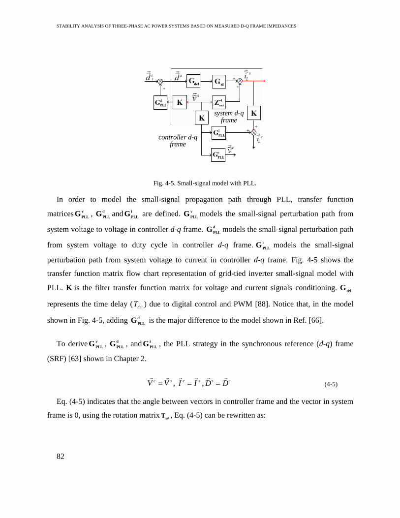
STABILITY ANALYSIS OF THREE-PHASE AC POWER SYSTEMS BASED ON MEASURED D-Q FRAME IMPEDANCES
82
+
++
+
+
+
system d-qframe
controller d-q frame
Fig. 4-5. Small-signal model with PLL.
In order to model the small-signal propagation path through PLL, transfer function
matrices v
PLLG , d
PLLG and i
PLLG are defined. v
PLLG models the small-signal perturbation path from
system voltage to voltage in controller d-q frame. d
PLLG models the small-signal perturbation path
from system voltage to duty cycle in controller d-q frame. i
PLLG models the small-signal
perturbation path from system voltage to current in controller d-q frame. Fig. 4-5 shows the
transfer function matrix flow chart representation of grid-tied inverter small-signal model with
PLL. K is the filter transfer function matrix for voltage and current signals conditioning. del
G
represents the time delay (del
T ) due to digital control and PWM [88]. Notice that, in the model
shown in Fig. 4-5, adding d
PLLG is the major difference to the model shown in Ref. [66].
To derive v
PLLG , d
PLLG , and i
PLLG , the PLL strategy in the synchronous reference (d-q) frame
(SRF) [63] shown in Chapter 2.
sc VV
, sc II
, cs DD
(4-5)
Eq. (4-5) indicates that the angle between vectors in controller frame and the vector in system
frame is 0, using the rotation matrix
T , Eq. (4-5) can be rewritten as:

83
sc VV
)0cos()0sin(
)0sin()0cos(, sc II
)0cos()0sin(
)0sin()0cos(,
cs DD
)0cos()0sin(
)0sin()0cos(
(4-6)
Add small-signal perturbation to Eq. (4-6):
s
q
s
q
s
d
s
d
c
q
c
q
c
d
c
d
vV
vV
vV
vV~
~
)~
0cos()~
0sin(
)~
0sin()~
0cos(~
~
(4-7)
By doing approximation of trigonometric functions, and canceling the steady state values,
relationship between voltage vectors in controller frame, system frame and PLL output angle can
be derived as:
s
q
s
q
s
d
s
d
c
q
c
q
c
d
c
d
vV
vV
vV
vV~
~
1~
~1
~
~
(4-8)
s
q
s
d
s
q
s
d
c
q
c
d
vV
Vv
v
v
~~
~~
~
~
(4-9)
Recall that PLL output angle is:
s
tfvPLL
c
q
1~~ (4-10)
Where,
s
kktfipllppllPLL
1 (4-11)
Substitute Eq. (4-10) to (4-9), Eq. (4-12) shows the equation represent the relation between
PLL output angle and q channel voltage.
s
q
PLL
s
d
PLL vtfVs
tf ~~
(4-12)
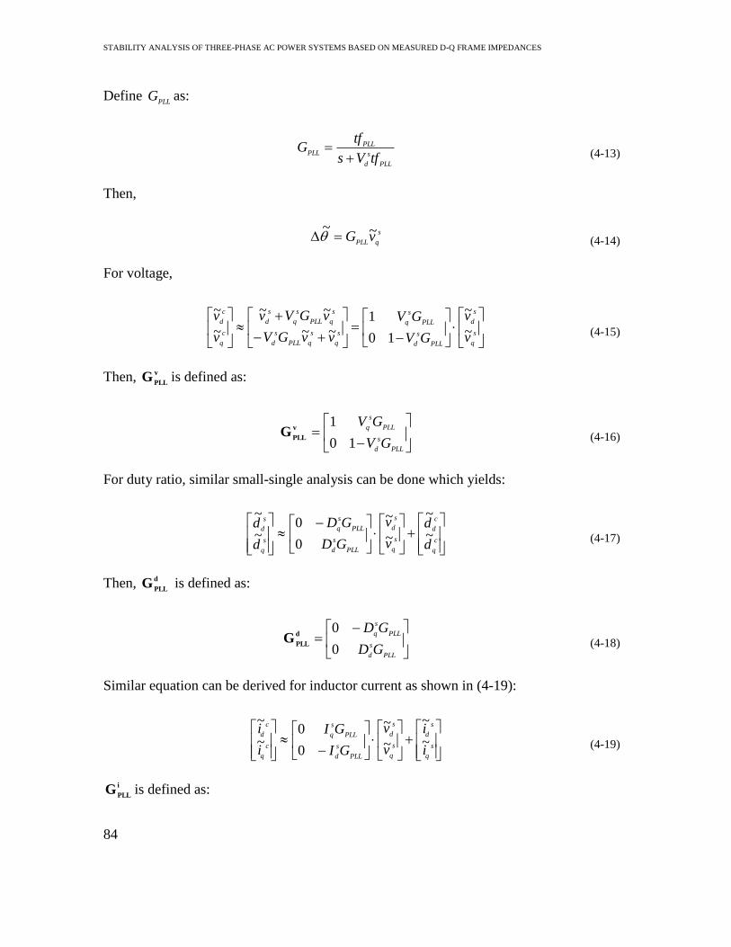
STABILITY ANALYSIS OF THREE-PHASE AC POWER SYSTEMS BASED ON MEASURED D-Q FRAME IMPEDANCES
84
Define PLL
G as:
PLL
s
d
PLL
PLLtfVs
tfG
(4-13)
Then,
s
qPLLvG ~~
(4-14)
For voltage,
s
q
s
d
PLL
s
d
PLL
s
q
s
q
s
qPLL
s
d
s
qPLL
s
q
s
d
c
q
c
d
v
v
GV
GV
vvGV
vGVv
v
v~
~
10
1~~
~~
~
~
(4-15)
Then, v
PLLG is defined as:
PLL
s
d
PLL
s
q
GV
GV
10
1v
PLLG (4-16)
For duty ratio, similar small-single analysis can be done which yields:
c
q
c
d
s
q
s
d
PLL
s
d
PLL
s
q
s
q
s
d
d
d
v
v
GD
GD
d
d~
~
~
~
0
0~
~
(4-17)
Then, d
PLLG is defined as:
PLL
s
d
PLL
s
q
GD
GD
0
0d
PLLG (4-18)
Similar equation can be derived for inductor current as shown in (4-19):
s
q
s
d
s
q
s
d
PLL
s
d
PLL
s
q
c
q
c
d
i
i
v
v
GI
GI
i
i~
~
~
~
0
0~
~
(4-19)
i
PLLG is defined as:
85
PLL
s
d
PLL
s
q
GI
GI
0
0i
PLLG (4-20)
Solving the equations represented by Fig. 4-5, the output impedance of inverter with PLL
working on open loop is:
1d
PLLdelid
1
outout_ol_PLLKGGGZZ
(4-21)
With DDSRF, the relation between PLL output angle and grid voltage is:
s
qPLL
s
dPLLvGvG ~~~
21 (4-22)
Where,
2122
21
1HVHVtfs
HtfG
s
q
s
dPLL
PLL
PLL
(4-23)
2122
22
2HVHVtfs
HtfG
s
q
s
dPLL
PLL
PLL
(4-24)
Then v
PLLG , d
PLLG , and i
PLLG become v
DDPLLG , d
DDPLLG , and i
DDPLLG with DDSRF PLL, and they
are:
21
21
1
1
PLL
s
dPLL
s
d
PLL
s
qPLL
s
q
GVGV
GVGVv
DDPLLG (4-25)
21
21
PLL
s
dPLL
s
d
PLL
s
qPLL
s
q
GDGD
GDGDd
DDPLLG (4-26)
21
21
PLL
s
dPLL
s
d
PLL
s
qPLL
s
q
GIGI
GIGIi
DDPLLG (4-27)
When DDSRF PLL is used, d
PLLG is replaced by d
DDPLLG in Eq. (4-21).
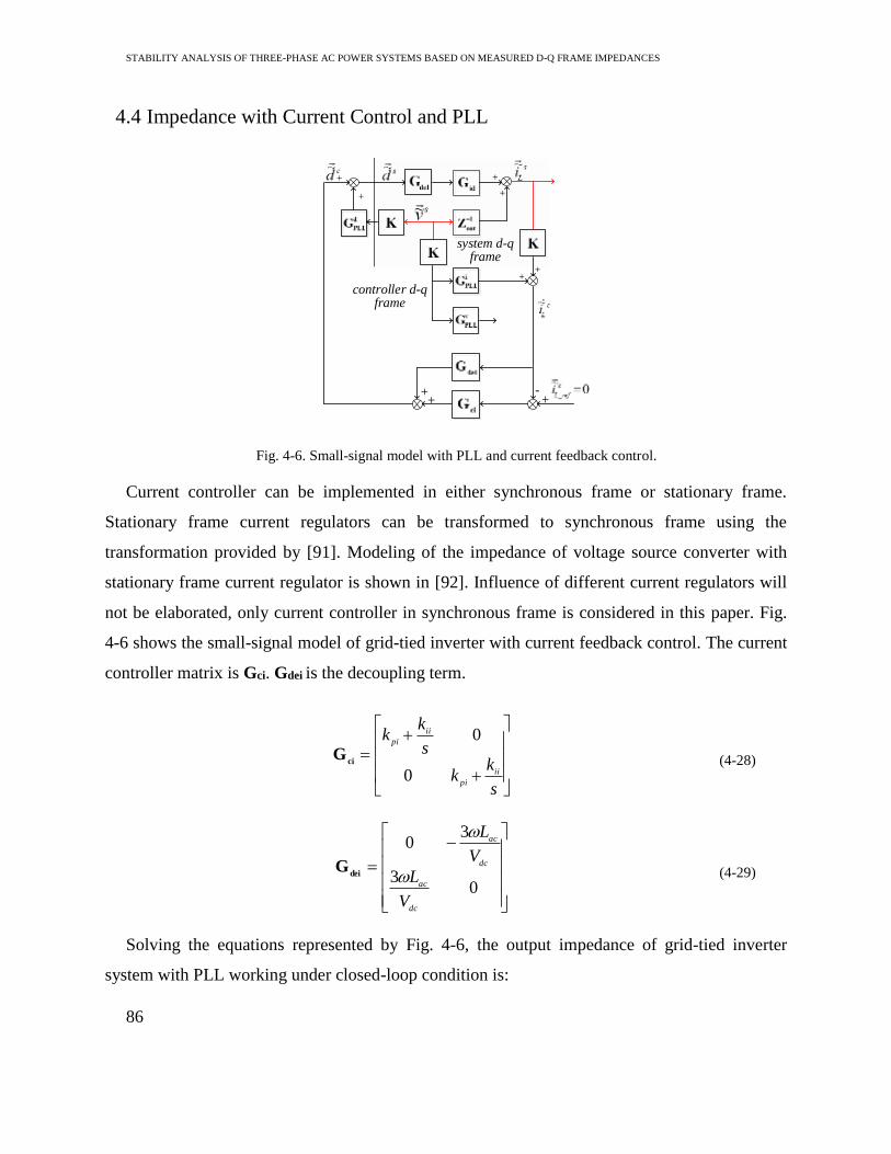
STABILITY ANALYSIS OF THREE-PHASE AC POWER SYSTEMS BASED ON MEASURED D-Q FRAME IMPEDANCES
86
4.4 Impedance with Current Control and PLL
+-
++
+
++
+
+
+
system d-qframe
controller d-q frame
Fig. 4-6. Small-signal model with PLL and current feedback control.
Current controller can be implemented in either synchronous frame or stationary frame.
Stationary frame current regulators can be transformed to synchronous frame using the
transformation provided by [91]. Modeling of the impedance of voltage source converter with
stationary frame current regulator is shown in [92]. Influence of different current regulators will
not be elaborated, only current controller in synchronous frame is considered in this paper. Fig.
4-6 shows the small-signal model of grid-tied inverter with current feedback control. The current
controller matrix is Gci. Gdei is the decoupling term.
s
kk
s
kk
ii
pi
ii
pi
0
0
ciG (4-28)
03
30
dc
ac
dc
ac
V
L
V
L
deiG (4-29)
Solving the equations represented by Fig. 4-6, the output impedance of grid-tied inverter
system with PLL working under closed-loop condition is:

87
KGGGGI
KGGGGGGZZ
deicidelid
1d
PLL
i
PLLdeicidelid
1
outout_il_PLL
(4-30)
When DDSRF PLL is used, d
PLLG is replaced by d
DDPLLG and i
PLLG is replaced by i
DDPLLG in Eq.
(4-30).
Table 4-1. Parameters of Grid-Tied Inverter Prototype
Symbol Description Value
Vdc Inverter input dc voltage 270 V
Vsd D channel grid voltage 99.6 V
Vsq Q channel grid voltage 0 V
idref D channel current reference -11 A
iqref Q channel current reference 0 A
ω Line frequency 2π×400 Hz
L Inductance of inverter output inductor 970 µH
RL Resistance of inverter output inductor self-resistor 120 mΩ
fsw Switching frequency 20 kHz
kpi Proportional gain of current controller 0.023
kii Integrator gain of current controller 25.59
ωn Natural frequency of signal conditioning filter 1.23e6 rad/s
ζ Damping factor of signal conditioning filter 4.74e-13
Tdel Time delay due to digital control and PWM 1.5/fsw
ωf Cut off frequency of LPF in DDSRF PLL 1777 rad/s
kppll Proportional gain of inverter PLL
kipll Integral gain of inverter PLL
Table 4-1 in shows the parameters of inverter prototype system. Using these parameters and
Eq. (4-30), Fig. 4-7 shows the Bode plot of inverter output impedances with current feedback
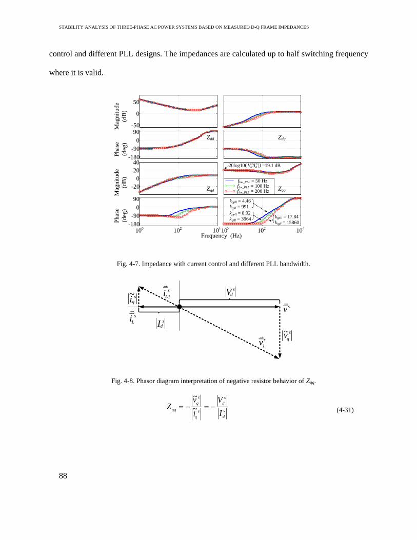
STABILITY ANALYSIS OF THREE-PHASE AC POWER SYSTEMS BASED ON MEASURED D-Q FRAME IMPEDANCES
88
control and different PLL designs. The impedances are calculated up to half switching frequency
where it is valid.
Frequency (Hz)
-50
0
50
-180
-90
0
90
-20
0
20
40
-180
-90
0
90
100
102
104
Mag
nit
ude
(dB
)
Phas
e
(deg
)
Mag
nit
ude
(dB
)
Phas
e
(deg
)
Zdd
Zqd
Zdq
Zqq
fbw_PLL = 50 Hzfbw_PLL = 100 Hzfbw_PLL = 200 Hz
100
102
104
kppll = 4.46
kipll = 991
kppll = 8.92
kipll = 3964kppll = 17.84
kipll = 15860
20log10 Is
dVs
d|( / |) =19.1 dB
Fig. 4-7. Impedance with current control and different PLL bandwidth.
sqi
~
s
qv~
sdV
sdI
sv_
1
sv_
s
Li_
1
s
Li_
Fig. 4-8. Phasor diagram interpretation of negative resistor behavior of Zqq.
s
d
s
d
s
q
s
q
qqI
V
i
vZ ~
~
(4-31)

89
-50
0
50
-180
-90
0
90
-20
0
20
40
-180
-90
0
90
Frequency (Hz)10
010
210
4
Mag
nit
ude
(dB
)
Phas
e
(deg
)
Mag
nit
ude
(dB
)
Phas
e
(deg
)
Zdd
Zqd
idref = -6A; iqref = 0Aidref = -11A; iqref = 0Aidref = -20A; iqref = 0A
100
102
104
Zdq
Zqq
Fig. 4-9. Impedance with current control and different current ratings.
As it can be observed in Fig. 4-7, Zdd shows the current source behavior. In low frequency
range, it is shaped by current controller integrator; in high frequency range, Zdd is the impedance
of ac inductor. Zdq and Zqd are very small within current controller bandwidth, because of unity
power factor control. In high frequency range, they behave as the power stage impedance value
as shown in Eq. (4-1). Zqq behaves as negative incremental resistance within PLL bandwidth.
Three different PLL designs which bandwidth (fbw_PLL) varies from 50 Hz to 200 Hz (line
frequency is set to be 400 Hz in order to allow a wide range of PLL bandwidth) are chosen to
show the influence of PLL. The results shows that higher PLL bandwidth case yields wider
frequency range of negative resistance behavior. The magnitude of the resistance related to
power rating of the inverter. Especially, as shown in Fig. 4-8, current vector of the inverter is
synchronized with grid voltage vector which is aligned in d channel to inject real power to the
grid. When voltage disturbance happens in q channel, the voltage vector sv
becomes sv1
. Because
of PLL, current vector will rotate to keep the synchronization with voltage vector. Meanwhile,
current controller keeps current magnitude in d channel unchanged. Then, current vector
s
Li
becomes s
Li
1
due to the q channel voltage perturbation. Notice that small-signal response of q
channel current is in the opposite direction of q channel voltage perturbation, so, from Fig. 4-8,
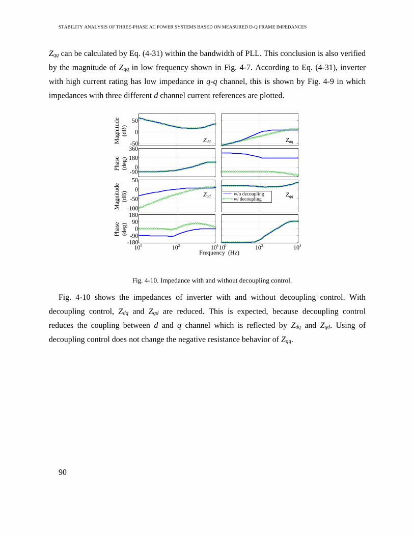
STABILITY ANALYSIS OF THREE-PHASE AC POWER SYSTEMS BASED ON MEASURED D-Q FRAME IMPEDANCES
90
Zqq can be calculated by Eq. (4-31) within the bandwidth of PLL. This conclusion is also verified
by the magnitude of Zqq in low frequency shown in Fig. 4-7. According to Eq. (4-31), inverter
with high current rating has low impedance in q-q channel, this is shown by Fig. 4-9 in which
impedances with three different d channel current references are plotted.
-50
0
50
-900
180
360
-100
-50
0
50
-180-90
090
180
Mag
nit
ud
e
(dB
)
Ph
ase
(deg
)
Mag
nit
ud
e
(dB
)
Ph
ase
(deg
)
w/o decouplingw/ decoupling
Frequency (Hz)10
010
210
410
010
210
4
Zdd
Zqd
Zdq
Zqq
Fig. 4-10. Impedance with and without decoupling control.
Fig. 4-10 shows the impedances of inverter with and without decoupling control. With
decoupling control, Zdq and Zqd are reduced. This is expected, because decoupling control
reduces the coupling between d and q channel which is reflected by Zdq and Zqd. Using of
decoupling control does not change the negative resistance behavior of Zqq.

91
-50
0
50
-180
-90
0
90
-20
0
20
40
-180
-90
0
90
SRF PLLDDSRF PLL
Frequency (Hz)10
010
210
410
010
210
4
Mag
nit
ude
(dB
)
Phas
e
(deg
)
Mag
nit
ude
(dB
)
Phas
e
(deg
)
Fig. 4-11. Impedance with current control and different PLL strategies.
Fig. 4-11 shows the impedance with different PLL strategies which indicates that using of
DDSRF PLL does not change the negative resistance behavior of Zqq.
Grid-tied inverter can inject reactive current to support the grid. Fig. 4-12 shows the
impedance of grid-tied inverter with different reactive power injections. Blue line shows the
impedance of capacitive power injection case; the green line shows the impedance of no reactive
power injection, and the red line shows the inductive power injection case. Notice that reactive
power injection will increase the impedance of cross coupling term Zdq, the rest impedances are
the same with unit power factor case. The negative resistance feature remains unchanged when
grid-tied inverter injects reactive power to the grid.
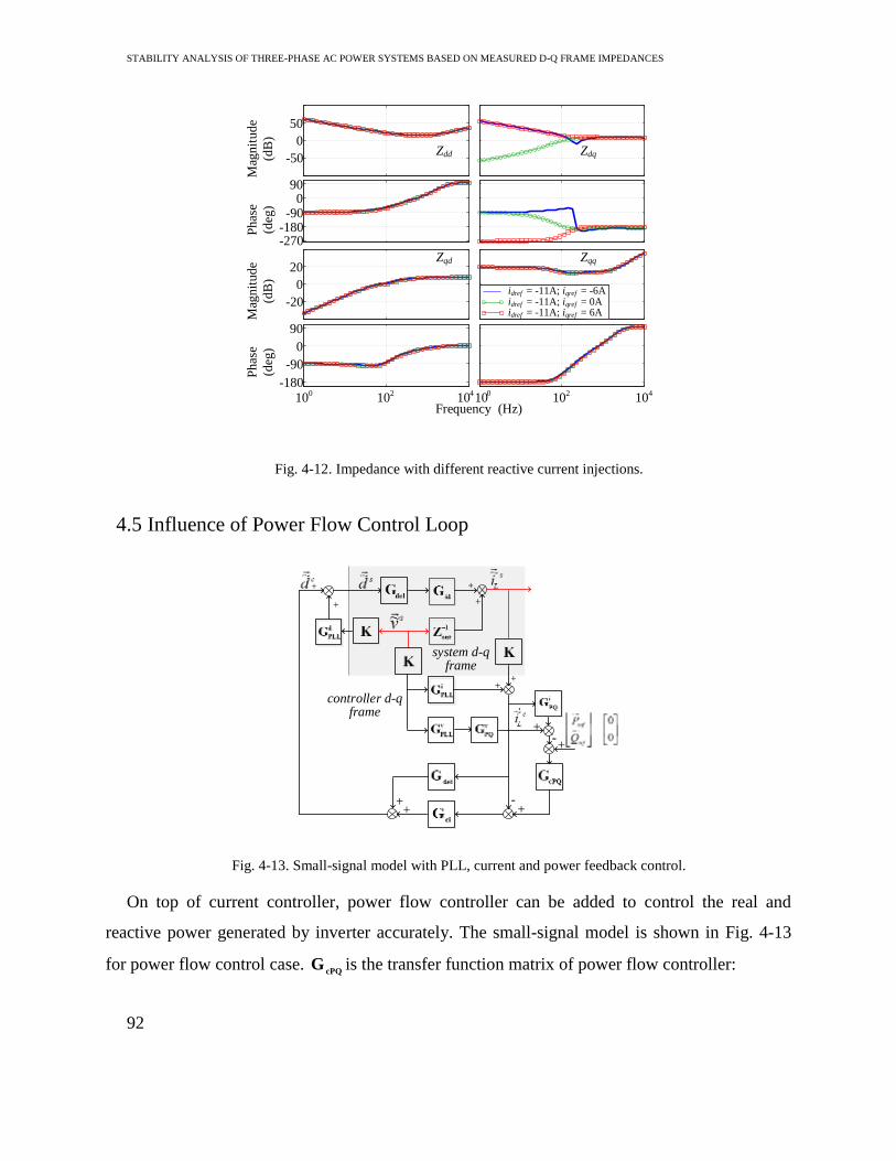
STABILITY ANALYSIS OF THREE-PHASE AC POWER SYSTEMS BASED ON MEASURED D-Q FRAME IMPEDANCES
92
-50
0
50
-270-180-90
090
-20
0
20
-180
-90
0
90
Frequency (Hz)10
010
210
4
Zdd
ZqdM
agn
itu
de
(dB
)
Ph
ase
(deg
)
Mag
nit
ud
e
(dB
)
Ph
ase
(deg
)
Zdq
Zqq
idref = -11A; iqref = -6Aidref = -11A; iqref = 0Aidref = -11A; iqref = 6A
100
102
104
Fig. 4-12. Impedance with different reactive current injections.
4.5 Influence of Power Flow Control Loop
+-
++
+
++
+
+
+
system d-qframe
controller d-q frame
+
+-
Fig. 4-13. Small-signal model with PLL, current and power feedback control.
On top of current controller, power flow controller can be added to control the real and
reactive power generated by inverter accurately. The small-signal model is shown in Fig. 4-13
for power flow control case. cPQ
G is the transfer function matrix of power flow controller:
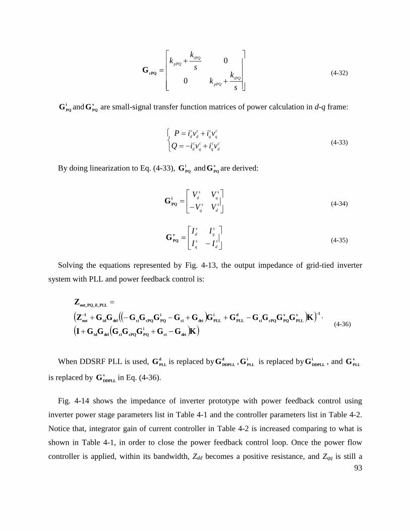
93
s
kk
s
kk
iPQ
pPQ
iPQ
pPQ
0
0
cPQG (4-32)
i
PQG and v
PQG are small-signal transfer function matrices of power calculation in d-q frame:
c
d
c
q
c
q
c
d
c
q
c
q
c
d
c
d
viviQ
viviP (4-33)
By doing linearization to Eq. (4-33), i
PQG and v
PQG are derived:
s
d
s
q
s
q
s
d
VV
VVi
PQG (4-34)
s
d
s
q
s
q
s
d
II
IIv
PQG
(4-35)
Solving the equations represented by Fig. 4-13, the output impedance of grid-tied inverter
system with PLL and power feedback control is:
KGGGGGGGI
KGGGGGGGGGGGGGZ
Z
deici
i
PQcPQcidelid
1v
PLL
v
PQcPQci
d
PLL
i
PLLdeici
i
PQcPQcidelid
1
out
PLLout_PQ_il_
(4-36)
When DDSRF PLL is used, d
PLLG is replaced by d
DDPLLG , i
PLLG is replaced by i
DDPLLG , and v
PLLG
is replaced by v
DDPLLG in Eq. (4-36).
Fig. 4-14 shows the impedance of inverter prototype with power feedback control using
inverter power stage parameters list in Table 4-1 and the controller parameters list in Table 4-2.
Notice that, integrator gain of current controller in Table 4-2 is increased comparing to what is
shown in Table 4-1, in order to close the power feedback control loop. Once the power flow
controller is applied, within its bandwidth, Zdd becomes a positive resistance, and Zqq is still a
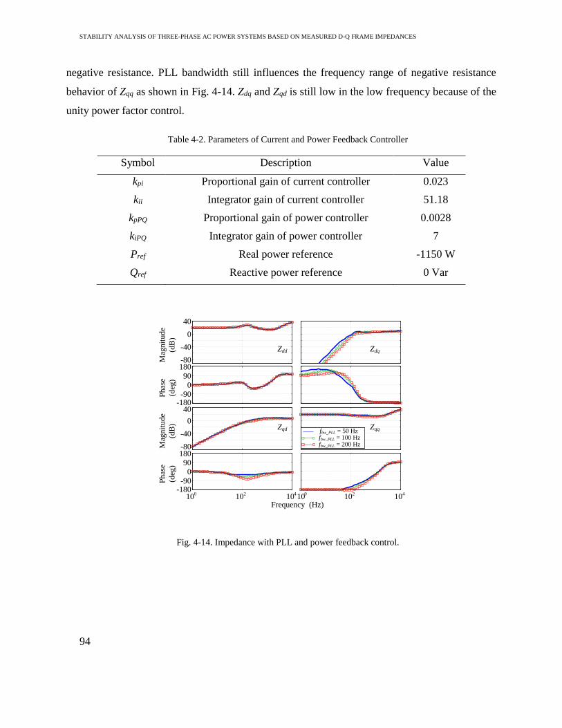
STABILITY ANALYSIS OF THREE-PHASE AC POWER SYSTEMS BASED ON MEASURED D-Q FRAME IMPEDANCES
94
negative resistance. PLL bandwidth still influences the frequency range of negative resistance
behavior of Zqq as shown in Fig. 4-14. Zdq and Zqd is still low in the low frequency because of the
unity power factor control.
Table 4-2. Parameters of Current and Power Feedback Controller
Symbol Description Value
kpi Proportional gain of current controller 0.023
kii Integrator gain of current controller 51.18
kpPQ Proportional gain of power controller 0.0028
kiPQ Integrator gain of power controller 7
Pref Real power reference -1150 W
Qref Reactive power reference 0 Var
-80
-40
0
40
-180-90
090
180
-80
-40
0
40
-180-90
090
180
Mag
nit
ud
e
(dB
)
Ph
ase
(deg
)
Mag
nit
ud
e
(dB
)
Ph
ase
(deg
)
Frequency (Hz)10
010
210
410
010
210
4
fbw_PLL = 50 Hzfbw_PLL = 100 Hzfbw_PLL = 200 Hz
Zdd
Zqd
Zdq
Zqq
Fig. 4-14. Impedance with PLL and power feedback control.
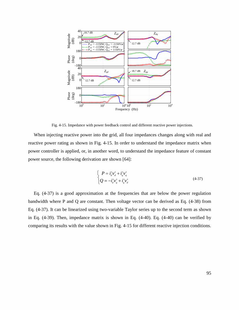
95
-180
0
180
0
20
40
-180
0
180
0
20
40
Frequency (Hz)10
010
210
410
010
210
4
Mag
nit
ud
e
(dB
)
Ph
ase
(deg
)
Mag
nit
ud
e
(dB
)
Ph
ase
(deg
) 18.7 dB
12.7 dB
12.7 dB
12.7 dB
18.7 dB
Pref = -1150W; Qref = -1150VarPref = -1150W; Qref = 0VarPref = -1150W; Qref = 1150Var
12.7 dB
Zdd
Zqd
Zdq
Zqq
Fig. 4-15. Impedance with power feedback control and different reactive power injections.
When injecting reactive power into the grid, all four impedances changes along with real and
reactive power rating as shown in Fig. 4-15. In order to understand the impedance matrix when
power controller is applied, or, in another word, to understand the impedance feature of constant
power source, the following derivation are shown [64]:
s
d
s
q
s
q
s
d
s
q
s
q
s
d
s
d
viviQ
viviP (4-37)
Eq. (4-37) is a good approximation at the frequencies that are below the power regulation
bandwidth where P and Q are constant. Then voltage vector can be derived as Eq. (4-38) from
Eq. (4-37). It can be linearized using two-variable Taylor series up to the second term as shown
in Eq. (4-39). Then, impedance matrix is shown in Eq. (4-40). Eq. (4-40) can be verified by
comparing its results with the value shown in Fig. 4-15 for different reactive injection conditions.
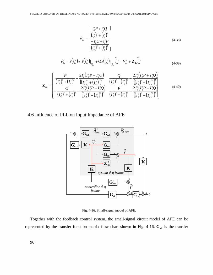
STABILITY ANALYSIS OF THREE-PHASE AC POWER SYSTEMS BASED ON MEASURED D-Q FRAME IMPEDANCES
96
22
22
s
q
s
d
s
q
s
d
s
q
s
d
s
q
s
d
s
dq
ii
PiQi
ii
QiPi
v
(4-38)
s
dq
s
dq
s
dqsdq
I
s
dqsdq
I
s
dq
s
dq
s
dqiViiiiv~~
|OF|FF
dqZ
(4-39)
2222222222
2222222222
22
22
s
q
s
d
s
d
s
q
s
q
s
q
s
ds
q
s
d
s
d
s
q
s
d
s
q
s
d
s
q
s
d
s
q
s
d
s
q
s
q
s
ds
q
s
d
s
q
s
d
s
d
s
q
s
d
II
QIPII
II
P
II
QIPII
II
Q
II
QIPII
II
Q
II
QIPII
II
P
dqZ (4-40)
4.6 Influence of PLL on Input Impedance of AFE
+
+
+
+
+-
+-
+
+
+
+
system d-q frame
controller d-q frame
Gvd
Gve
G id
Z in
-1
Gdel
K
K
KK
GPLL
i
GPLL
d
Gci Gcv
vdcAFE
s~dAFE
s~→
i s~→
0
ic~→
vs~→
Fig. 4-16. Small-signal model of AFE.
Together with the feedback control system, the small-signal circuit model of AFE can be
represented by the transfer function matrix flow chart shown in Fig. 4-16. vd
G is the transfer

97
function matrix from duty ratio vector s
AFEd
~
to output dc voltage s
dcAFEv~ ;
veG is the transfer
function matrix from PCC voltage vector sv~ to output dc voltage s
dcAFEv~ ;
idG is the transfer
function matrix from duty ratio vector s
AFEd
~
to inductor current vector si~
, in
Z is the output
impedance of power stage. d
PLLG is the transfer function matrix from system voltage sv
~ to system
d-q frame duty ratio vector s
AFEd
~
; i
PLLG is the transfer function matrix from system voltage sv
~ to
controller d-q frame current vector ci
~
. From Fig. 4-16, Eq. (4-45) can be derived to calculate the
input impedance of AFE with feedback control.
PLL
s
dAFE
PLL
s
qAFE
GD
GD
0
0d
PLLG
(4-41)
PLL
s
d
PLL
s
q
GI
GI
0
0i
PLLG
(4-42)
PLL
s
d
PLL
PLLtfVs
tfG
(4-43)
skktfipllAFEppllAFEPLL
/ (4-44)
KGGKGGGGIGI
KGKGGGKGG
GKGGGGIGZZ
cidel
1
vdcvcidelid
1
d
PLLvecvci
i
PLLci
del
1
vdcvcidelid
1
in
AFEdq
(4-45)
Using the parameters in Table 5-1, input impedances of AFE are plotted in Fig. 4-17.
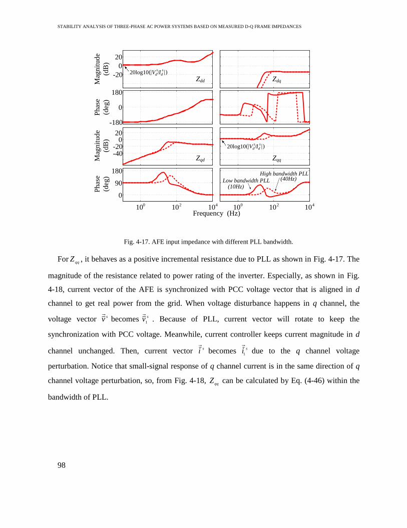
STABILITY ANALYSIS OF THREE-PHASE AC POWER SYSTEMS BASED ON MEASURED D-Q FRAME IMPEDANCES
98
-20
0
20
-180
0
180
-40-20
020
0
90
180
Frequency (Hz)10
010
210
410
410
210
0
Mag
nit
ude
(dB
)
Phas
e
(deg
)
Mag
nit
ude
(dB
)
Phas
e
(deg
)
High bandwidth PLL(40Hz)Low bandwidth PLL
(10Hz)
Zdd Zdq
Zqd Zqq
20log10 Is
dVs
d|( / |)
20log10 Is
dVs
d|( / |)
Fig. 4-17. AFE input impedance with different PLL bandwidth.
Forqq
Z , it behaves as a positive incremental resistance due to PLL as shown in Fig. 4-17. The
magnitude of the resistance related to power rating of the inverter. Especially, as shown in Fig.
4-18, current vector of the AFE is synchronized with PCC voltage vector that is aligned in d
channel to get real power from the grid. When voltage disturbance happens in q channel, the
voltage vector sv
becomes sv1
. Because of PLL, current vector will rotate to keep the
synchronization with PCC voltage. Meanwhile, current controller keeps current magnitude in d
channel unchanged. Then, current vector si
becomes si
1
due to the q channel voltage
perturbation. Notice that small-signal response of q channel current is in the same direction of q
channel voltage perturbation, so, from Fig. 4-18, qq
Z can be calculated by Eq. (4-46) within the
bandwidth of PLL.
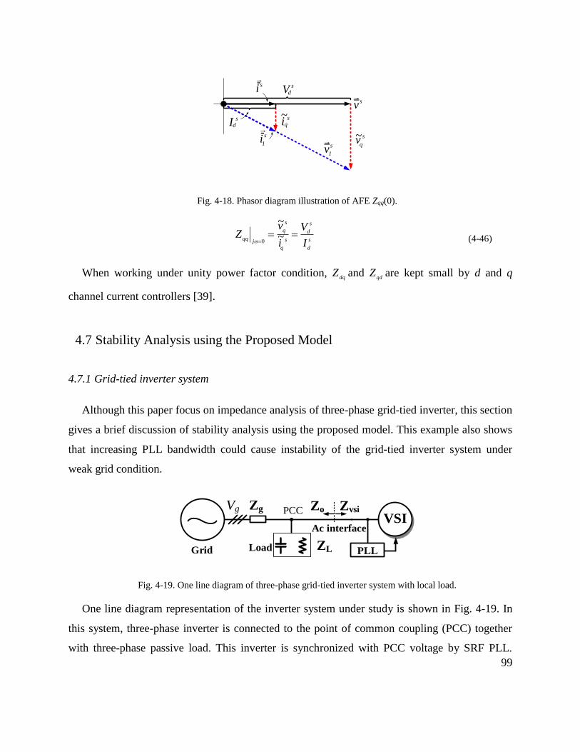
99
s
qv~
sdI
s
dV
sqi
~
si-1
s
i-
sv_
1
sv_
Fig. 4-18. Phasor diagram illustration of AFE Zqq(0).
s
d
s
d
s
q
s
q
jqqI
V
i
vZ
~
~
0 (4-46)
When working under unity power factor condition, dq
Z and qd
Z are kept small by d and q
channel current controllers [39].
4.7 Stability Analysis using the Proposed Model
4.7.1 Grid-tied inverter system
Although this paper focus on impedance analysis of three-phase grid-tied inverter, this section
gives a brief discussion of stability analysis using the proposed model. This example also shows
that increasing PLL bandwidth could cause instability of the grid-tied inverter system under
weak grid condition.
Grid ZL
ZgVg PCC Zo Zvsi
VSI
PLLLoad
Ac interface
Fig. 4-19. One line diagram of three-phase grid-tied inverter system with local load.
One line diagram representation of the inverter system under study is shown in Fig. 4-19. In
this system, three-phase inverter is connected to the point of common coupling (PCC) together
with three-phase passive load. This inverter is synchronized with PCC voltage by SRF PLL.

STABILITY ANALYSIS OF THREE-PHASE AC POWER SYSTEMS BASED ON MEASURED D-Q FRAME IMPEDANCES
100
Only current feedback control is applied to control the amount of power injection to PCC. Each
phase of the passive load consist of parallel connected resistor and capacitor. Grid is connected
to PCC through impedance consist of inductor and resistor. The detailed parameter of this system
is shown in Table 4-3.
Table 4-3. Parameters of Inverter System for Stability Analysis
Symbol Description Value
Vg Grid line-line peak voltage 6120 V
ωg Grid voltage frequency 2π×60 Hz
L Inductance of inverter 1 mH
Vdc Inverter dc voltage 600 V
fsw Switching frequency of inverter 20 kHz
Idref d channel current of inverter -190 A
Iqref q channel current of inverter 0 A
kpi Proportional gain of inverter current controller 0.0105
kii Integrator gain of inverter current controller 1.1519
kppll Proportional gain of inverter PLL 1.5 (stable);
3 (unstable)
kipll Integral gain of inverter PLL 3.2
ZL Local passive load RLoad: 10 Ω;
CLoad: 250 μF
Zg Grid impedance Rg: 0.2 Ω;
Lg: 2 mH
fpll PLL output frequency of inverter
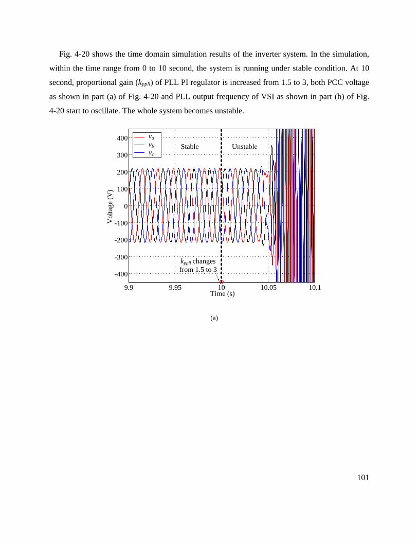
101
Fig. 4-20 shows the time domain simulation results of the inverter system. In the simulation,
within the time range from 0 to 10 second, the system is running under stable condition. At 10
second, proportional gain (kppll) of PLL PI regulator is increased from 1.5 to 3, both PCC voltage
as shown in part (a) of Fig. 4-20 and PLL output frequency of VSI as shown in part (b) of Fig.
4-20 start to oscillate. The whole system becomes unstable.
-400
-300
-200
-100
0
100
200
300
400
Volt
age
(V)
va
vb
vc
kppll changes
from 1.5 to 3
9.9 9.95 10 10.05 10.1Time (s)
Stable Unstable
(a)

STABILITY ANALYSIS OF THREE-PHASE AC POWER SYSTEMS BASED ON MEASURED D-Q FRAME IMPEDANCES
102
9.9 9.95 10 10.05 10.1
-400
-300
-200
-100
0
100
200
300
400
Time (s)
Cu
rren
t (A
)
ia
ib
ic
kppll changes
from 1.5 to 3
Stable Unstable
(b)
9.9 9.95 10 10.05 10.1
45
50
55
60
65
70
75
Time (s)
Fre
quen
cy (
Hz)
fpll
kppll changes
from 1.5 to 3
Stable Unstable
(b)
Fig. 4-20. (a) PCC voltages; (b) output current of VSI; (c) PLL output frequency of VSI.
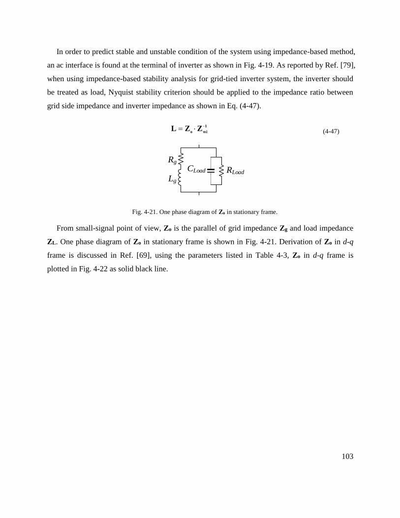
103
In order to predict stable and unstable condition of the system using impedance-based method,
an ac interface is found at the terminal of inverter as shown in Fig. 4-19. As reported by Ref. [79],
when using impedance-based stability analysis for grid-tied inverter system, the inverter should
be treated as load, Nyquist stability criterion should be applied to the impedance ratio between
grid side impedance and inverter impedance as shown in Eq. (4-47).
1
vsioZZL
(4-47)
CLoad RLoad
Lg
Rg
Fig. 4-21. One phase diagram of Zo in stationary frame.
From small-signal point of view, Zo is the parallel of grid impedance Zg and load impedance
ZL. One phase diagram of Zo in stationary frame is shown in Fig. 4-21. Derivation of Zo in d-q
frame is discussed in Ref. [69], using the parameters listed in Table 4-3, Zo in d-q frame is
plotted in Fig. 4-22 as solid black line.
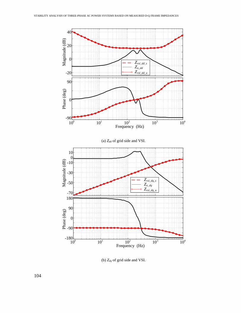
STABILITY ANALYSIS OF THREE-PHASE AC POWER SYSTEMS BASED ON MEASURED D-Q FRAME IMPEDANCES
104
-20
0
20
40
Mag
nit
ude
(dB
)
-90
0
90
Phas
e (d
eg)
Frequency (Hz)10
410
310
210
110
0
Zvsi_dd_s
Zo_dd
Zvsi_dd_u
(a) Zdd of grid side and VSI.
-70
-50
-30
-10
0
10
Mag
nit
ud
e (d
B)
-180
-90
0
90
180
Ph
ase
(deg
)
Zvsi_dq_s
Zo_dq
Zvsi_dq_u
Frequency (Hz)10
410
310
210
110
0
(b) Zdq of grid side and VSI.

105
-80
-40
0
Mag
nit
ud
e (d
B)
-180
-90
0
90
180
Phas
e (d
eg)
Frequency (Hz)10
410
310
210
110
0
Zvsi_qd_s
Zo_qd
Zvsi_qd_u
(c) Zqd of grid side and VSI.
-10
0
10
30
Mag
nit
ude
(dB
)
-180
-90
0
90
Phas
e (d
eg)
Frequency (Hz)10
410
310
210
110
0
Zvsi_qq_s
Zo_qq
Zvsi_qq_u
kppll =1.5kppll =3
kppll =1.5
kppll =3
(d) Zqq of grid side and VSI.
Fig. 4-22. Impedances of the source and load.
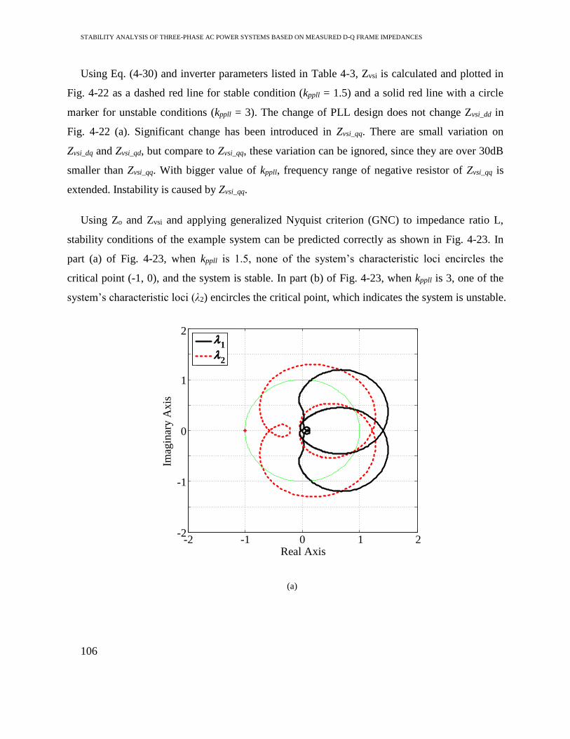
STABILITY ANALYSIS OF THREE-PHASE AC POWER SYSTEMS BASED ON MEASURED D-Q FRAME IMPEDANCES
106
Using Eq. (4-30) and inverter parameters listed in Table 4-3, Zvsi is calculated and plotted in
Fig. 4-22 as a dashed red line for stable condition (kppll = 1.5) and a solid red line with a circle
marker for unstable conditions (kppll = 3). The change of PLL design does not change Zvsi_dd in
Fig. 4-22 (a). Significant change has been introduced in Zvsi_qq. There are small variation on
Zvsi_dq and Zvsi_qd, but compare to Zvsi_qq, these variation can be ignored, since they are over 30dB
smaller than Zvsi_qq. With bigger value of kppll, frequency range of negative resistor of Zvsi_qq is
extended. Instability is caused by Zvsi_qq.
Using Zo and Zvsi and applying generalized Nyquist criterion (GNC) to impedance ratio L,
stability conditions of the example system can be predicted correctly as shown in Fig. 4-23. In
part (a) of Fig. 4-23, when kppll is 1.5, none of the system’s characteristic loci encircles the
critical point (-1, 0), and the system is stable. In part (b) of Fig. 4-23, when kppll is 3, one of the
system’s characteristic loci (λ2) encircles the critical point, which indicates the system is unstable.
-2 -1 0 1 2-2
-1
0
1
2
1
2
Real Axis
Imag
inar
y A
xis
(a)

107
1
2
-2 -1 0 1 2-2
-1
0
1
2
Real Axis
Imag
inar
y A
xis
(b)
Fig. 4-23. GNC plots: (a) stable case (kpll = 1.5); (b) unstable case (kpll = 3).
In this example, grid-tied inverter is controlled with current controller, the negative resistor is
only observed on Zqq, not Zdd. Zdq and Zqd are controlled with very small magnitude under unity
power factor. Instability of the system is mainly due to Zqq. When the inverter injects reactive
power, magnitude of Zdq becomes significant, but it is still not negative resistor. When power
controllers are added and inverter injects reactive power, Zdq and Zqd could also behave as
negative resistor as shown in Fig. 4-15. The impacts of Zdq and Zqd on system stability under
these condition need more discussion in the future.
4.8 Experimental Verification
4.8.1 Grid-tied inverter system
In order to verify the proposed model, low power prototype of three-phase grid-tied inverter
and d-q impedance measurement equipment [46] are built as shown in Fig. 4-24.
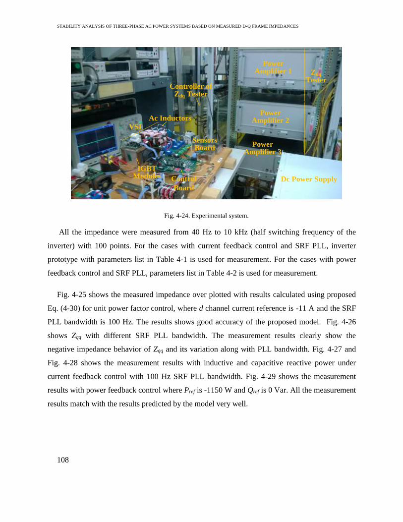
STABILITY ANALYSIS OF THREE-PHASE AC POWER SYSTEMS BASED ON MEASURED D-Q FRAME IMPEDANCES
108
Dc Power Supply
VSI
Zdq
Tester
Power Amplifier 1
Power Amplifier 2
Power Amplifier 3
Controller of Zdq Tester
Control
Board
Ac Inductors
Sensors Board
IGBT Modules
Fig. 4-24. Experimental system.
All the impedance were measured from 40 Hz to 10 kHz (half switching frequency of the
inverter) with 100 points. For the cases with current feedback control and SRF PLL, inverter
prototype with parameters list in Table 4-1 is used for measurement. For the cases with power
feedback control and SRF PLL, parameters list in Table 4-2 is used for measurement.
Fig. 4-25 shows the measured impedance over plotted with results calculated using proposed
Eq. (4-30) for unit power factor control, where d channel current reference is -11 A and the SRF
PLL bandwidth is 100 Hz. The results shows good accuracy of the proposed model. Fig. 4-26
shows Zqq with different SRF PLL bandwidth. The measurement results clearly show the
negative impedance behavior of Zqq and its variation along with PLL bandwidth. Fig. 4-27 and
Fig. 4-28 shows the measurement results with inductive and capacitive reactive power under
current feedback control with 100 Hz SRF PLL bandwidth. Fig. 4-29 shows the measurement
results with power feedback control where Pref is -1150 W and Qref is 0 Var. All the measurement
results match with the results predicted by the model very well.
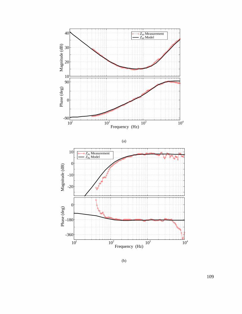
109
10
20
30
40
Mag
nit
ud
e (d
B)
-90
0
90
Ph
ase
(deg
)
Frequency (Hz)10
110
210
310
4
Zdd Measurement Zdd Model
(a)
-20
-10
0
10
-360
-180
0
Mag
nit
ud
e (d
B)
Ph
ase
(deg
)
Frequency (Hz)10
110
210
310
4
Zdq Measurement Zdq Model
(b)

STABILITY ANALYSIS OF THREE-PHASE AC POWER SYSTEMS BASED ON MEASURED D-Q FRAME IMPEDANCES
110
-10
0
10
-180
-90
0
90
Mag
nit
ud
e (d
B)
Ph
ase
(deg
)
Frequency (Hz)10
110
210
310
4
Zqd Measurement Zqd Model
(c)
10
20
30
-180
-90
0
90
Mag
nit
ud
e (d
B)
Ph
ase
(deg
)
Frequency (Hz)10
110
210
310
4
Zqq Measurement Zqq Model
(d)
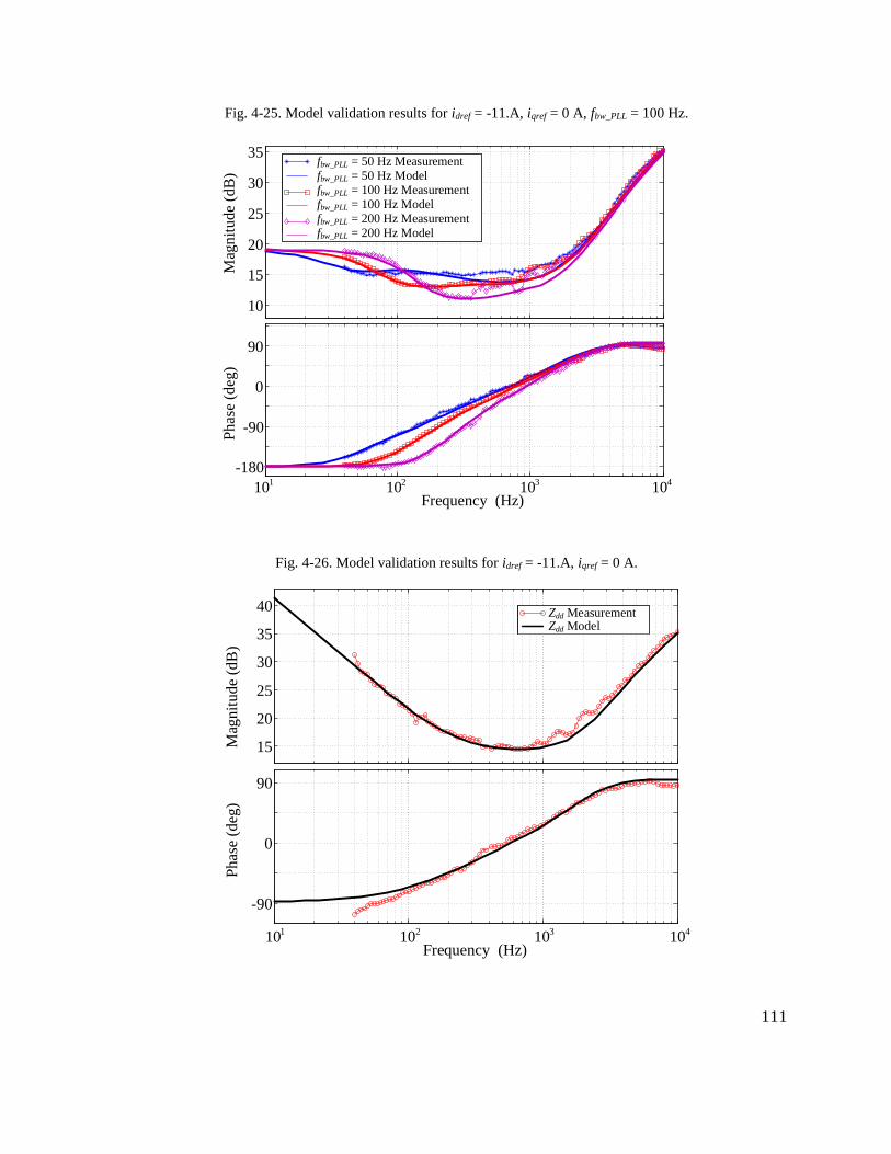
111
Fig. 4-25. Model validation results for idref = -11.A, iqref = 0 A, fbw_PLL = 100 Hz.
10
15
20
25
30
35
Mag
nit
ude
(dB
)
-180
-90
0
90
Phas
e (d
eg)
Frequency (Hz)10
110
210
310
4
fbw_PLL = 50 Hz Measurement
fbw_PLL = 50 Hz Model
fbw_PLL = 100 Hz Measurement
fbw_PLL = 100 Hz Model
fbw_PLL = 200 Hz Measurement
fbw_PLL = 200 Hz Model
Fig. 4-26. Model validation results for idref = -11.A, iqref = 0 A.
15
20
25
30
35
40
-90
0
90
Mag
nit
ud
e (d
B)
Ph
ase
(deg
)
Frequency (Hz)10
110
210
310
4
Zdd Measurement Zdd Model

STABILITY ANALYSIS OF THREE-PHASE AC POWER SYSTEMS BASED ON MEASURED D-Q FRAME IMPEDANCES
112
(a)
0
10
20
30
-180
-90
0
90
180
Mag
nit
ud
e (d
B)
Ph
ase
(deg
)
Frequency (Hz)10
110
210
310
4
Zdq Measurement Zdq Model
(b)
-10
-5
0
5
10
15
-180
-90
0
90
180
Mag
nit
ud
e (d
B)
Ph
ase
(deg
)
Frequency (Hz)10
110
210
310
4
Zqd Measurement Zqd Model
(c)
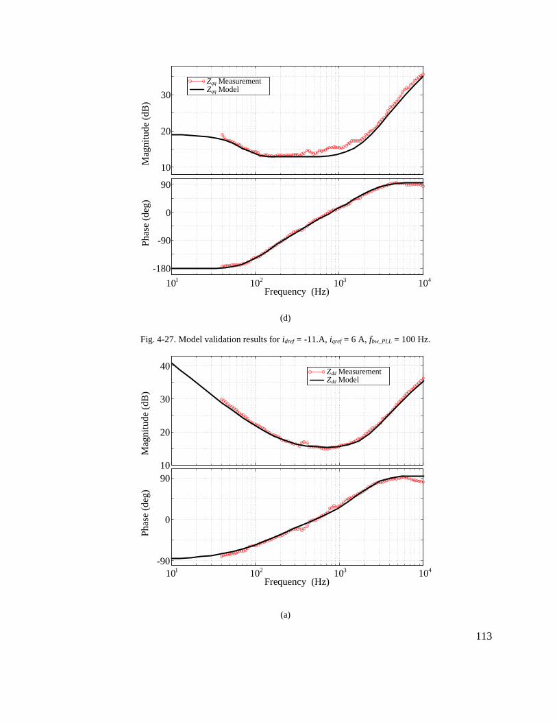
113
10
20
30
-180
-90
0
90
Mag
nit
ud
e (d
B)
Ph
ase
(deg
)
Frequency (Hz)10
110
210
310
4
Zqq Measurement Zqq Model
(d)
Fig. 4-27. Model validation results for idref = -11.A, iqref = 6 A, fbw_PLL = 100 Hz.
10
20
30
40
-90
0
90
Zdd Measurement Zdd Model
Mag
nit
ude
(dB
)P
has
e (d
eg)
Frequency (Hz)10
110
210
310
4
(a)

STABILITY ANALYSIS OF THREE-PHASE AC POWER SYSTEMS BASED ON MEASURED D-Q FRAME IMPEDANCES
114
-10
0
10
20
30
-180
-90
0
Zdq Measurement Zdq Model
Mag
nit
ude
(dB
)P
has
e (d
eg)
Frequency (Hz)10
110
210
310
4
(b)
-5
0
5
10
-180
-90
0
Zqd Measurement Zqd ModelM
agn
itu
de
(dB
)P
has
e (d
eg)
Frequency (Hz)10
110
210
310
4
(c)
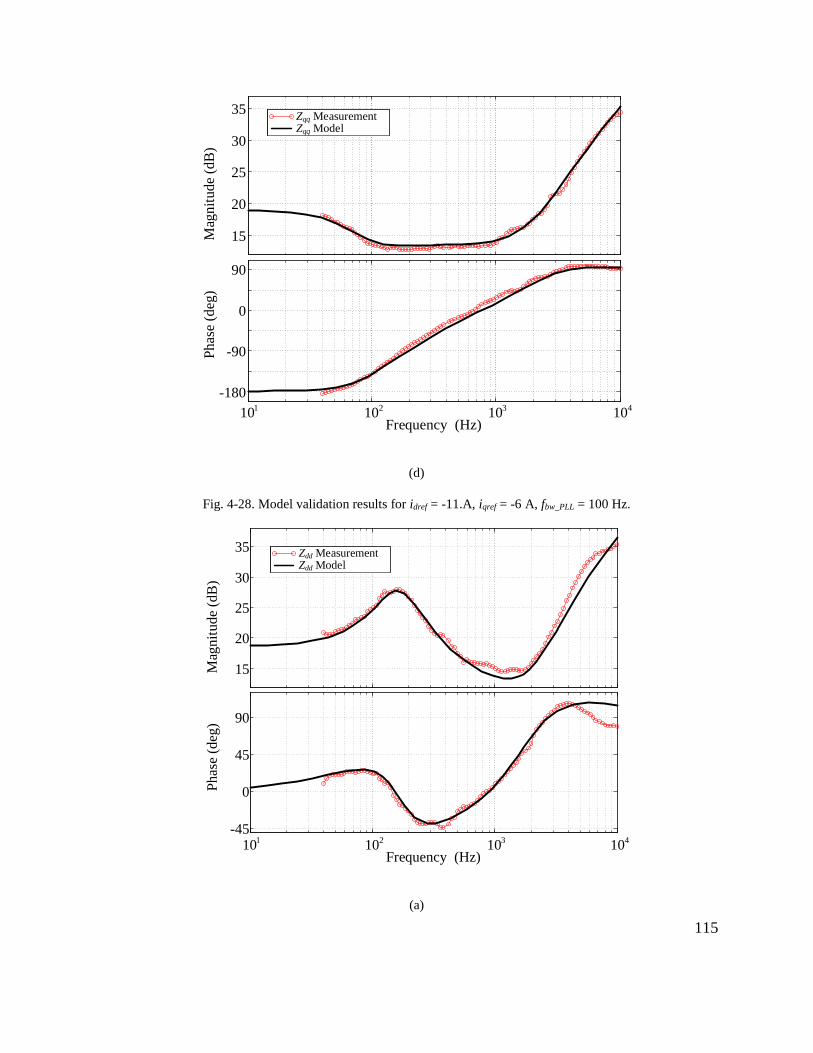
115
15
20
25
30
35
-180
-90
0
90
Zqq Measurement Zqq Model
Mag
nit
ude
(dB
)P
has
e (d
eg)
Frequency (Hz)10
110
210
310
4
(d)
Fig. 4-28. Model validation results for idref = -11.A, iqref = -6 A, fbw_PLL = 100 Hz.
15
20
25
30
35
-45
0
45
90
Mag
nit
ud
e (d
B)
Ph
ase
(deg
)
Frequency (Hz)10
110
210
310
4
Zdd Measurement Zdd Model
(a)
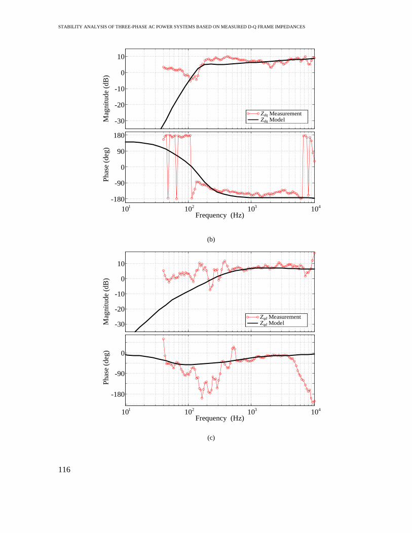
STABILITY ANALYSIS OF THREE-PHASE AC POWER SYSTEMS BASED ON MEASURED D-Q FRAME IMPEDANCES
116
-30
-20
-10
0
10
-180
-90
0
90
180
Mag
nit
ud
e (d
B)
Ph
ase
(deg
)
Frequency (Hz)10
110
210
310
4
Zdq Measurement Zdq Model
(b)
-30
-20
-10
0
10
-180
-90
0
Mag
nit
ud
e (d
B)
Ph
ase
(deg
)
Frequency (Hz)10
110
210
310
4
Zqd Measurement Zqd Model
(c)

117
15
20
25
30
35
-180
-90
0
90
Mag
nit
ude
(dB
)P
has
e (d
eg)
Frequency (Hz)10
110
210
310
4
Zqq Measurement Zqq Model
(d)
Fig. 4-29. Model validation results for Pdref = -1150 W, Qqref = 0 Var, fbw_PLL = 100 Hz.
4.8.2 AFE
To verify the proposed input impedance model for AFE, measurements are carried out on the
built test-bed with the parameters list in Table 4-4. The results are shown in Fig. 4-30 for
impedances and Fig. 4-31 for admittances. Fig. 4-32 shows the Zqq of AFE with different PLL
bandwidth. All the results show good agreement between model and measurement.

STABILITY ANALYSIS OF THREE-PHASE AC POWER SYSTEMS BASED ON MEASURED D-Q FRAME IMPEDANCES
118
Table 4-4. Parameters of AFE system for measurement
Symbol Description Value
Vll Grid line-line peak voltage 65.57 V
fg Grid voltage frequency 60 Hz
fsw Switching frequency of AFE 20 kHz
LAFE Inductance of AFE 0.47 mH
Cdc Dc link capacitor of AFE 100 μF
Rdc Load resistor of AFE 96 Ω
VdcAFE Dc voltage of AFE 270 V
kpiAFE Proportional gain of AFE current controller 0.0116
kiiAFE Integrator gain of AFE current controller 23.2711
kpvAFE Proportional gain of AFE voltage controller 0.0628
kivAFE Integrator gain of AFE voltage controller 3.2725
kppllAFE Proportional gain of AFE PLL 0.8921
kipllAFE Integral gain AFE of PLL 39.64

119
-40
0
40
Mag
nit
ude
(dB
)
-180
0
180
Phas
e
(deg
)
Frequency (Hz)
-40
0
40
Mag
nit
ude
(dB
)
-180
0
180P
has
e
(deg
)
Zdd Zdq
Zqd Zqq
modelmeasurement
104103102101104103102101
Fig. 4-30. Model validation results for ZdqAFE.
-100
-60
-20
-1800
180
-100
-60
-20
-1800
180
Frequency (Hz)104103102101104103102101
Mag
nit
ud
e
(dB
)
Ph
ase
(deg
)
Mag
nit
ud
e
(dB
)
Ph
ase
(deg
)
modelmeasurement
Ydd Ydq
Yqd Yqq
Fig. 4-31. Model validation results for YdqAFE
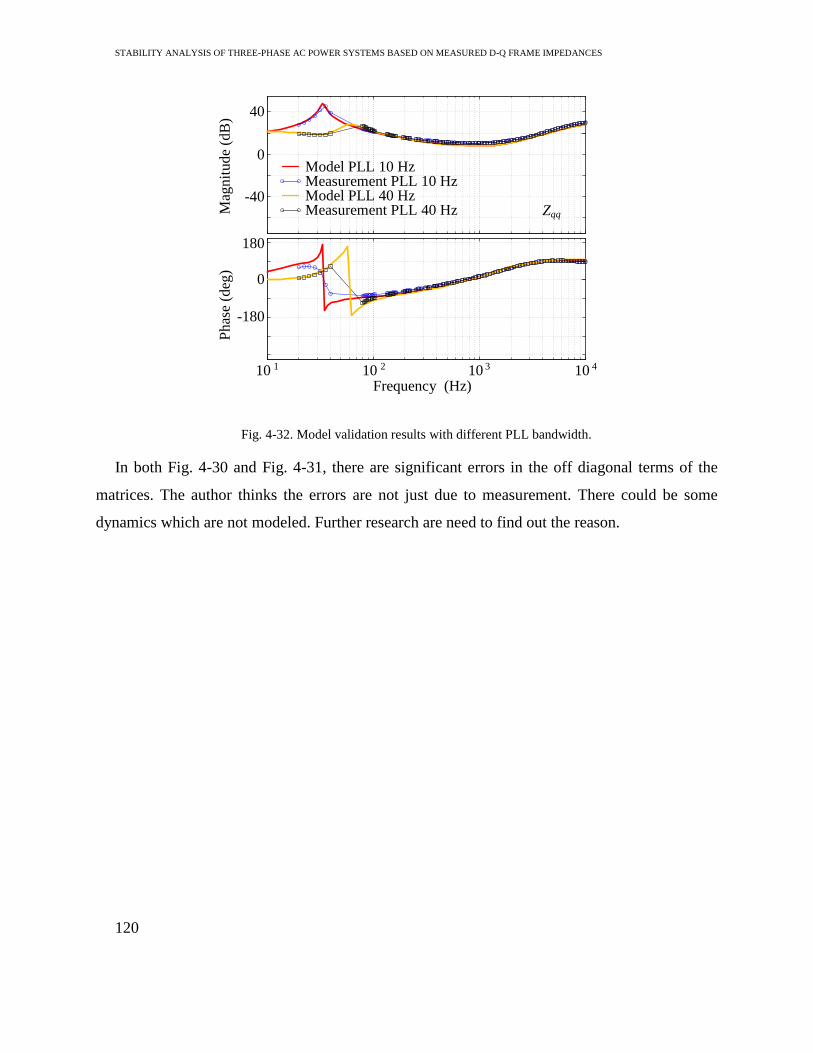
STABILITY ANALYSIS OF THREE-PHASE AC POWER SYSTEMS BASED ON MEASURED D-Q FRAME IMPEDANCES
120
-40
0
40
Mag
nit
ude
(dB
)
-180
0
180
Phas
e (d
eg)
Frequency (Hz)10 1 10 2 10 3 10 4
Zqq
Model PLL 10 HzMeasurement PLL 10 HzModel PLL 40 HzMeasurement PLL 40 Hz
Fig. 4-32. Model validation results with different PLL bandwidth.
In both Fig. 4-30 and Fig. 4-31, there are significant errors in the off diagonal terms of the
matrices. The author thinks the errors are not just due to measurement. There could be some
dynamics which are not modeled. Further research are need to find out the reason.

121
Chapter 5 Synchronization Stability Issues Caused by PLL
Dynamics
5.1 Introduction
More and more VSCs are installed to modern power systems. VSCs not only can improve the
power utilization efficiency but also are key components to integrate new energy sources The
systems like which has been shown in Fig. 5-1 have superior features to build the modern power
grids, including controllability, sustainability, and the improved efficiency. However, many
stability issues are reported regarding this system.
Interactions between VSCs and grid could make the system unstable. AFE can destabilize the
system due to its constant power load (CPL) behavior as discussed in chapter 3. PLLs are needed
for VSCs to synchronize with the grid. Chapter 4 shows that PLL shapes Zqq of grid-tied inverter
as negative increamental resistor within its bandwidth. Together with large grid side impedances,
this negative resistor could destabilize the inverter system. PLL shapes Zqq of AFE as positive
increamental resistor within its bandwidth. Changing PLL bandwidth could also lead the AFE
system in to instability when the source side output impedance is high.
Off Shore IslandDistribution Grid
Grid
Passive Load
VSI
PLLVSI
AFE
PLLAFE
Solar Inverter
Rectifier
ZgVg
PCC
Fig. 5-1. Distribution system with high penetration of VSCs.
STABILITY ANALYSIS OF THREE-PHASE AC POWER SYSTEMS BASED ON MEASURED D-Q FRAME IMPEDANCES
122
Designs of PLL for VSI and AFE usually consider the grid impedance is zero. When PLLs are
designed to be stable with certain margin by checking the loop gains of PLLs, VSI and AFE
should synchronize with the ideal grid. Due to the parallel connection, VSI and AFE utilize the
same voltage information at the point of common coupling (PCC) to do synchronization. Under
weak grid condition, grid impedance cannot be ignored. PCC voltage is then not only determined
by the grid voltage, but also grid impedance Zg and current injected by VSI and AFE. In this
way, PLLs of VSI and AFE couple with each other. With certain grid side impedance Zg, these
PLLs could be unstable which eventually makes the whole system lose synchronization and
collapse [68], although they are designed to be stable under the assumption that grid impedance
is zero. Ref. [68] proposes a PLL small-signal model including grid side impedances. The model
gives deep insight of the coupling nature of grid-connected VSCs through their PLLs.
Synchronization instability issue caused by PLL can be predicted using the model. However, the
proposed analysis uses characteristic equation of PLLs which involves control parameters of
every converter. For system integration, converters in the system are usually acquired as “black
boxes”. It may be found that the system oscillates or becomes unstable because the particular
grid or load impedances were not foreseen by the converters’ designers. Under such condition,
design specifications for each converter to avoid instability cannot be defined easily using
characteristic equation based method.
On the other hand, the impedance-based method, which does not need converters’ internal
design information, applies Nyquist stability criteria to the ratio between output impedance of the
source and the load input impedance for the stability analysis. Such method is well established
for converter-filter or general source-load interaction problems in dc electronic power conversion
systems [28], [35]–[37]. It is preferred by system integrator for the reason that stability issue can
be predicted based on measured impedances of the source and load [10].
In the case of three-phase ac systems, the impedance-based stability can be formulated using
the synchronous d-q frame source and load impedances, where the generalized Nyquist stability
criterion (GNC) or generalized inverse Nyquist stability criterion (GINC) is applied to return-
ratio matrix defined by the product of the source impedance and load admittance [2]–[43]. This
method was used to study the stability of a hybrid ac/dc system in Ref. [3], and the resonances
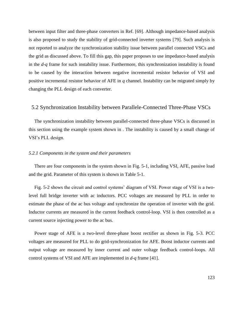
123
between input filter and three-phase converters in Ref. [69]. Although impedance-based analysis
is also proposed to study the stability of grid-connected inverter systems [79]. Such analysis is
not reported to analyze the synchronization stability issue between parallel connected VSCs and
the grid as discussed above. To fill this gap, this paper proposes to use impedance-based analysis
in the d-q frame for such instability issue. Furthermore, this synchronization instability is found
to be caused by the interaction between negative incremental resistor behavior of VSI and
positive incremental resistor behavior of AFE in q channel. Instability can be migrated simply by
changing the PLL design of each converter.
5.2 Synchronization Instability between Parallele-Connected Three-Phase VSCs
The synchronization instability between parallel-connected three-phase VSCs is discussed in
this section using the example system shown in . The instability is caused by a small change of
VSI’s PLL design.
5.2.1 Components in the system and their parameters
There are four components in the system shown in Fig. 5-1, including VSI, AFE, passive load
and the grid. Parameter of this system is shown in Table 5-1.
Fig. 5-2 shows the circuit and control systems’ diagram of VSI. Power stage of VSI is a two-
level full bridge inverter with ac inductors. PCC voltages are measured by PLL in order to
estimate the phase of the ac bus voltage and synchronize the operation of inverter with the grid.
Inductor currents are measured in the current feedback control-loop. VSI is then controlled as a
current source injecting power to the ac bus.
Power stage of AFE is a two-level three-phase boost rectifier as shown in Fig. 5-3. PCC
voltages are measured for PLL to do grid-synchronization for AFE. Boost inductor currents and
output voltage are measured by inner current and outer voltage feedback control-loops. All
control systems of VSI and AFE are implemented in d-q frame [41].
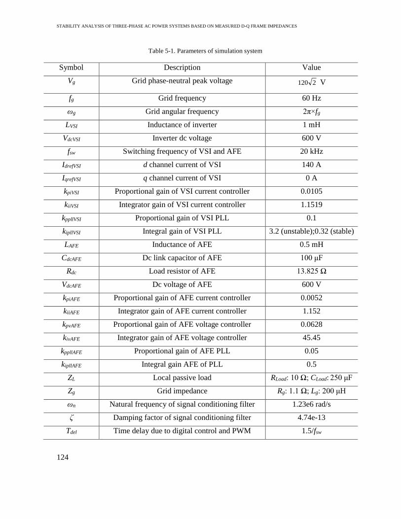
STABILITY ANALYSIS OF THREE-PHASE AC POWER SYSTEMS BASED ON MEASURED D-Q FRAME IMPEDANCES
124
Table 5-1. Parameters of simulation system
Symbol Description Value
Vg Grid phase-neutral peak voltage 2120 V
fg Grid frequency 60 Hz
ωg Grid angular frequency 2π×fg
LVSI Inductance of inverter 1 mH
VdcVSI Inverter dc voltage 600 V
fsw Switching frequency of VSI and AFE 20 kHz
IdrefVSI d channel current of VSI 140 A
IqrefVSI q channel current of VSI 0 A
kpiVSI Proportional gain of VSI current controller 0.0105
kiiVSI Integrator gain of VSI current controller 1.1519
kppllVSI Proportional gain of VSI PLL 0.1
kipllVSI Integral gain of VSI PLL 3.2 (unstable);0.32 (stable)
LAFE Inductance of AFE 0.5 mH
CdcAFE Dc link capacitor of AFE 100 μF
Rdc Load resistor of AFE 13.825 Ω
VdcAFE Dc voltage of AFE 600 V
kpiAFE Proportional gain of AFE current controller 0.0052
kiiAFE Integrator gain of AFE current controller 1.152
kpvAFE Proportional gain of AFE voltage controller 0.0628
kivAFE Integrator gain of AFE voltage controller 45.45
kppllAFE Proportional gain of AFE PLL 0.05
kipllAFE Integral gain AFE of PLL 0.5
ZL Local passive load RLoad: 10 Ω; CLoad: 250 μF
Zg Grid impedance Rg: 1.1 Ω; Lg: 200 μH
ωn Natural frequency of signal conditioning filter 1.23e6 rad/s
ζ Damping factor of signal conditioning filter 4.74e-13
Tdel Time delay due to digital control and PWM 1.5/fsw
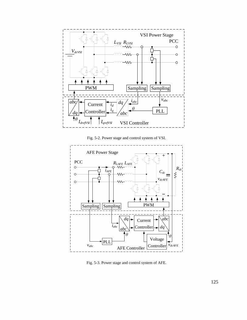
125
abc
dq
dq
abc
PWM
vabciabc
Sampling Sampling
Current
Controller
LVSI RLVSI
VdcVSI
θPLL
id
iq
IdrefVSI IqrefVSIθ
VSI Power Stage
VSI Controller
PCC
Fig. 5-2. Power stage and control system of VSI.
AFE Power Stage
PWM
AFE Controller
PLLvdcAFE
iabc
vabc
abc
dq
Voltage
Controller
Current
Controller
LAFERLAFE
RdcCdc
θ θ
vdcAFE
iAFE
Sampling Sampling
PCC
abc
dq
Fig. 5-3. Power stage and control system of AFE.
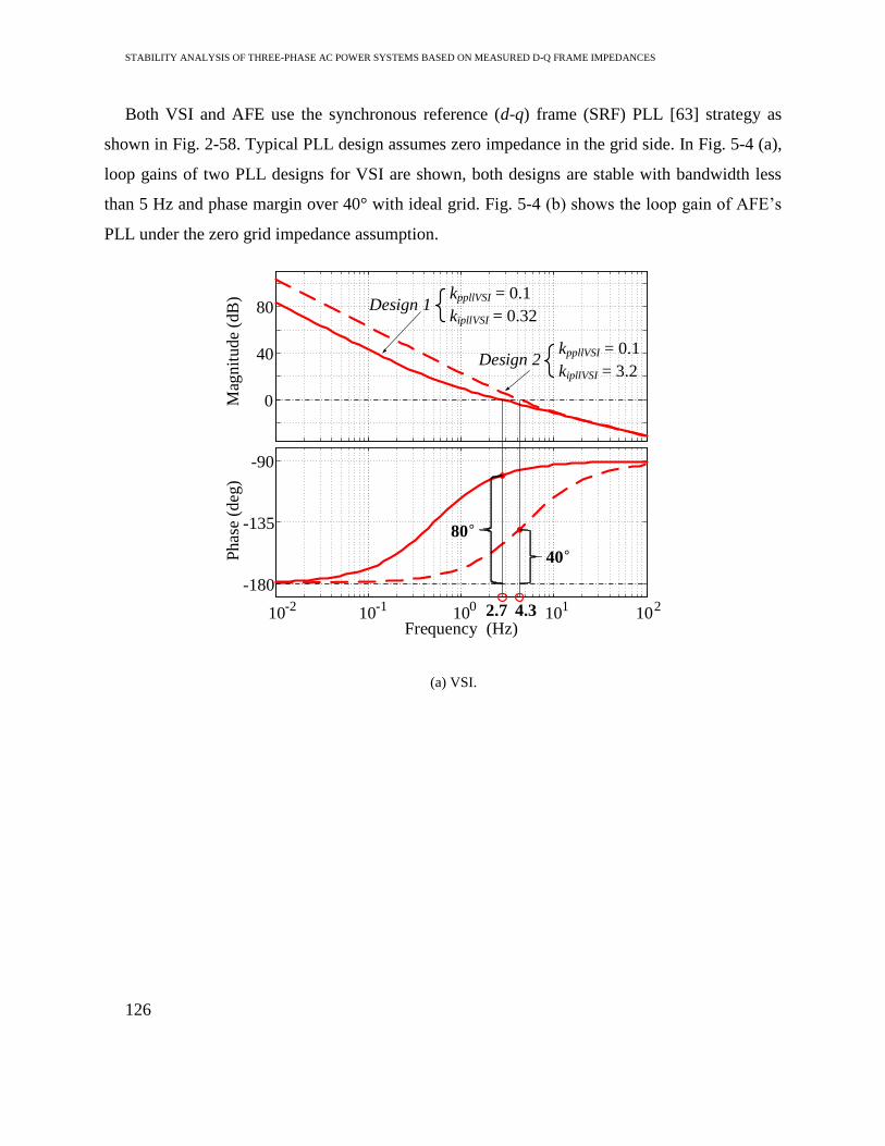
STABILITY ANALYSIS OF THREE-PHASE AC POWER SYSTEMS BASED ON MEASURED D-Q FRAME IMPEDANCES
126
Both VSI and AFE use the synchronous reference (d-q) frame (SRF) PLL [63] strategy as
shown in Fig. 2-58. Typical PLL design assumes zero impedance in the grid side. In Fig. 5-4 (a),
loop gains of two PLL designs for VSI are shown, both designs are stable with bandwidth less
than 5 Hz and phase margin over 40° with ideal grid. Fig. 5-4 (b) shows the loop gain of AFE’s
PLL under the zero grid impedance assumption.
80°
0
40
80
Frequency (Hz)
-180
-135
-90
102
101
100
10-1
10-2
Mag
nit
ud
e (d
B)
Phas
e (d
eg)
40°
2.7 4.3
kppllVSI = 0.1
kipllVSI = 3.2Design 2
kppllVSI = 0.1
kipllVSI = 0.32Design 1
(a) VSI.
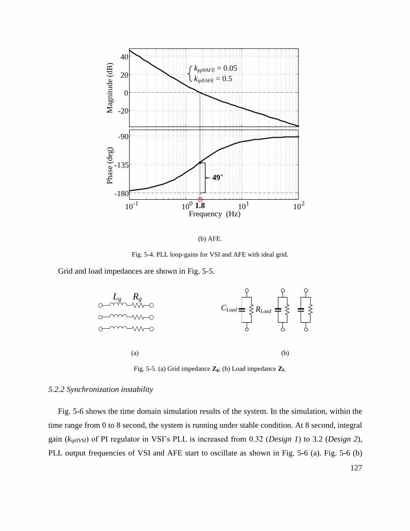
127
-20
0
20
40
Mag
nit
ude
(dB
)
Frequency (Hz)
-180
-135
-90
Phas
e (d
eg)
10-1
100
101
102
49°
1.8
kppllAFE = 0.05
kipllAFE = 0.5
(b) AFE.
Fig. 5-4. PLL loop-gains for VSI and AFE with ideal grid.
Grid and load impedances are shown in Fig. 5-5.
Lg Rg
CLoad RLoad
(a) (b)
Fig. 5-5. (a) Grid impedance Zg; (b) Load impedance ZL.
5.2.2 Synchronization instability
Fig. 5-6 shows the time domain simulation results of the system. In the simulation, within the
time range from 0 to 8 second, the system is running under stable condition. At 8 second, integral
gain (kipllVSI) of PI regulator in VSI’s PLL is increased from 0.32 (Design 1) to 3.2 (Design 2),
PLL output frequencies of VSI and AFE start to oscillate as shown in Fig. 5-6 (a). Fig. 5-6 (b)
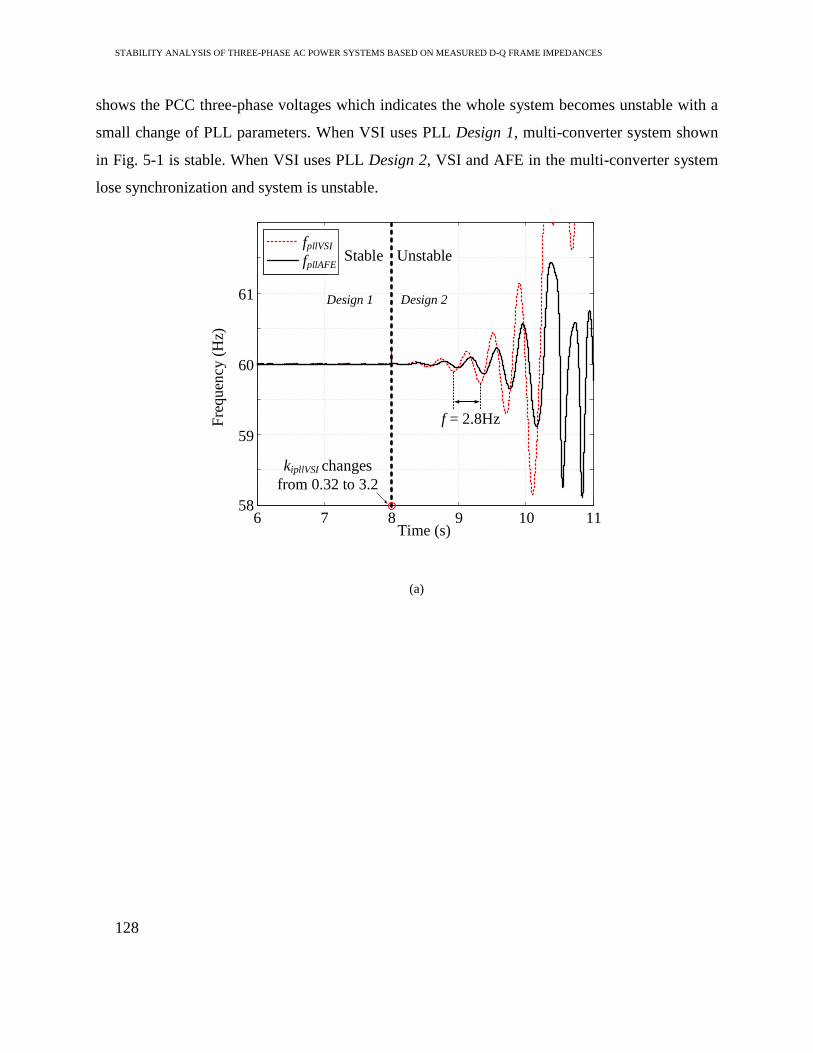
STABILITY ANALYSIS OF THREE-PHASE AC POWER SYSTEMS BASED ON MEASURED D-Q FRAME IMPEDANCES
128
shows the PCC three-phase voltages which indicates the whole system becomes unstable with a
small change of PLL parameters. When VSI uses PLL Design 1, multi-converter system shown
in Fig. 5-1 is stable. When VSI uses PLL Design 2, VSI and AFE in the multi-converter system
lose synchronization and system is unstable.
6 7 8 9 10 1158
59
60
61
Time (s)
Fre
qu
ency
(H
z)
f = 2.8Hz
kipllVSI changes
from 0.32 to 3.2
Stable UnstablefpllVSI
fpllAFE
Design 1 Design 2
(a)

129
-300
-200
-100
0
100
200
300
Volt
age
(V)
f = 2.8Hz
kipllVSI changes
from 0.32 to 3.2
Stable Unstable
6 7 8 9 10 11Time (s)
Design 1 Design 2
(b)
Fig. 5-6. (a) PLLs’ output frequencies; (b) PCC voltages.
5.3 PLL-Based Stability Analysis
The low frequency synchronization instability as shown in section 5.2 can be analyzed using
PLLs’ small-signal model [68]. This method is briefly summarized here.
Zg
ZL
IVSI VgVPCC
VSI GridLoad
θVSI θg
PLLVSI
θg
Gg1~
G11
θVSI
~
(a) Single line circuit. (b) SFG.
Fig. 5-7. Representations of VSI with local load connecting to the grid.
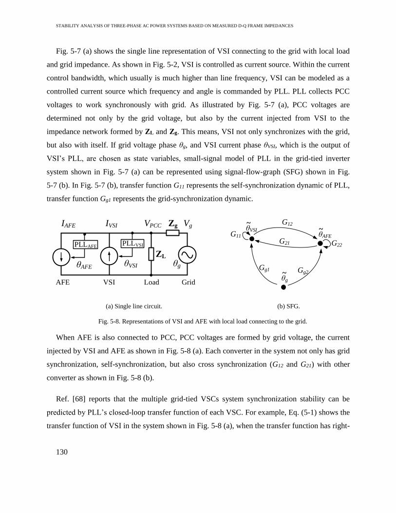
STABILITY ANALYSIS OF THREE-PHASE AC POWER SYSTEMS BASED ON MEASURED D-Q FRAME IMPEDANCES
130
Fig. 5-7 (a) shows the single line representation of VSI connecting to the grid with local load
and grid impedance. As shown in Fig. 5-2, VSI is controlled as current source. Within the current
control bandwidth, which usually is much higher than line frequency, VSI can be modeled as a
controlled current source which frequency and angle is commanded by PLL. PLL collects PCC
voltages to work synchronously with grid. As illustrated by Fig. 5-7 (a), PCC voltages are
determined not only by the grid voltage, but also by the current injected from VSI to the
impedance network formed by ZL and Zg. This means, VSI not only synchronizes with the grid,
but also with itself. If grid voltage phase θg, and VSI current phase θVSI, which is the output of
VSI’s PLL, are chosen as state variables, small-signal model of PLL in the grid-tied inverter
system shown in Fig. 5-7 (a) can be represented using signal-flow-graph (SFG) shown in Fig.
5-7 (b). In Fig. 5-7 (b), transfer function G11 represents the self-synchronization dynamic of PLL,
transfer function Gg1 represents the grid-synchronization dynamic.
Zg
ZL
IVSI VgVPCC
VSI GridLoad
θVSI θg
PLLVSI
θAFE
PLLAFE
AFE
IAFE
G21
θg
Gg1 Gg2~
G11
G12
G22
θVSI
~
θAFE
~
(a) Single line circuit. (b) SFG.
Fig. 5-8. Representations of VSI and AFE with local load connecting to the grid.
When AFE is also connected to PCC, PCC voltages are formed by grid voltage, the current
injected by VSI and AFE as shown in Fig. 5-8 (a). Each converter in the system not only has grid
synchronization, self-synchronization, but also cross synchronization (G12 and G21) with other
converter as shown in Fig. 5-8 (b).
Ref. [68] reports that the multiple grid-tied VSCs system synchronization stability can be
predicted by PLL’s closed-loop transfer function of each VSC. For example, Eq. (5-1) shows the
transfer function of VSI in the system shown in Fig. 5-8 (a), when the transfer function has right-

131
half plane pole (RHP), low frequency synchronization instability discussed in section 5.2
happens. Detailed analysis can be found in Ref. [68].
sD
sN
GGGGGG
GGGGgg
g
VSI
221122112112
212221
1
1~
~
(5-1)
This PLL small-signal model based analysis gives a deep insight to the PLL interaction
between grid and converters. On the other hand, this method needs not only the impedance of
grid, the impedance of local passive load, but also the parameters of every converter’s PLL
which may not available to system integrator. SFG of two-converter system is not simple
already. The scale of SFG will increase exponentially when number of converters increases.
Then, to find the model of the system is not easy. In addition, from this method, design
specification for each converter cannot be made to guarantee system synchronization stability.
5.4 Impedance-Based Analysis
Impedance-based small-signal stability analysis, first proposed by Ref. [28] for filter and dc-
dc converter system, models the system into two subsystem as shown in Fig. 5-9. The source
subsystem is modeled by its Thevenin equivalent circuit, which consists of an ideal voltage
source (vs) in series with an output impedance (Zs). Load subsystem is modeled by its input
impedance. Then the interface voltage (vl) can be derived as Eq. (5-2). If the minor loop gain, or
return ratio [3], is defined as Eq. (5-3), which is the ratio between source and load impedances,
the condition for system stability can be determined by checking whether the minor loop gain
(L(s)) satisfies the Nyquist stability criterion or not.
)()()(1)( 1 svsZsZsv slsl
1 (5-2)
)()()( 1 sZsZsL ls
(5-3)
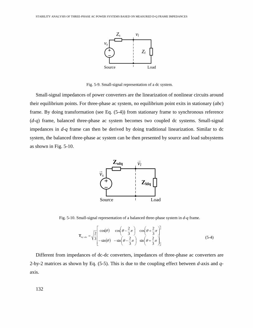
STABILITY ANALYSIS OF THREE-PHASE AC POWER SYSTEMS BASED ON MEASURED D-Q FRAME IMPEDANCES
132
Zs
Source Load
Zl
vs
vl
Fig. 5-9. Small-signal representation of a dc system.
Small-signal impedances of power converters are the linearization of nonlinear circuits around
their equilibrium points. For three-phase ac system, no equilibrium point exits in stationary (abc)
frame. By doing transformation (see Eq. (5-4)) from stationary frame to synchronous reference
(d-q) frame, balanced three-phase ac system becomes two coupled dc systems. Small-signal
impedances in d-q frame can then be derived by doing traditional linearization. Similar to dc
system, the balanced three-phase ac system can be then presented by source and load subsystems
as shown in Fig. 5-10.
Zsdq
Zldq
Source Load
vs→
vl→
Fig. 5-10. Small-signal representation of a balanced three-phase system in d-q frame.
3
2sin
3
2sinsin
3
2cos
3
2coscos
3
2/ abcdq
T
(5-4)
Different from impedances of dc-dc converters, impedances of three-phase ac converters are
2-by-2 matrices as shown by Eq. (5-5). This is due to the coupling effect between d-axis and q-
axis.
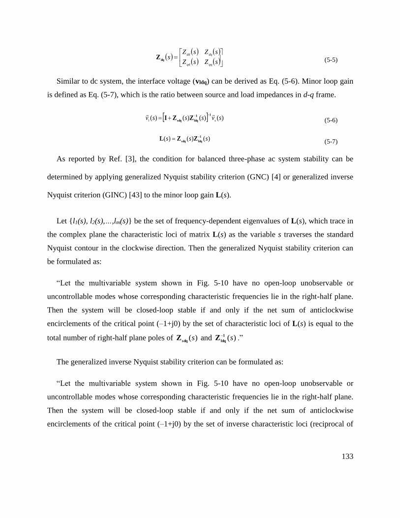
133
sZsZ
sZsZs
qqqd
dqdd
dqZ
(5-5)
Similar to dc system, the interface voltage (vldq) can be derived as Eq. (5-6). Minor loop gain
is defined as Eq. (5-7), which is the ratio between source and load impedances in d-q frame.
)()()()( svsssvsl
11
ldqsdqZZI
(5-6)
)()()( sss 1
ldqsdqZZL
(5-7)
As reported by Ref. [3], the condition for balanced three-phase ac system stability can be
determined by applying generalized Nyquist stability criterion (GNC) [4] or generalized inverse
Nyquist criterion (GINC) [43] to the minor loop gain L(s).
Let l1(s), l2(s),…,lm(s) be the set of frequency-dependent eigenvalues of L(s), which trace in
the complex plane the characteristic loci of matrix L(s) as the variable s traverses the standard
Nyquist contour in the clockwise direction. Then the generalized Nyquist stability criterion can
be formulated as:
“Let the multivariable system shown in Fig. 5-10 have no open-loop unobservable or
uncontrollable modes whose corresponding characteristic frequencies lie in the right-half plane.
Then the system will be closed-loop stable if and only if the net sum of anticlockwise
encirclements of the critical point (–1+j0) by the set of characteristic loci of L(s) is equal to the
total number of right-half plane poles of )(ssdq
Z and )(s1
ldqZ
.”
The generalized inverse Nyquist stability criterion can be formulated as:
“Let the multivariable system shown in Fig. 5-10 have no open-loop unobservable or
uncontrollable modes whose corresponding characteristic frequencies lie in the right-half plane.
Then the system will be closed-loop stable if and only if the net sum of anticlockwise
encirclements of the critical point (–1+j0) by the set of inverse characteristic loci (reciprocal of

STABILITY ANALYSIS OF THREE-PHASE AC POWER SYSTEMS BASED ON MEASURED D-Q FRAME IMPEDANCES
134
each of the numbers l1(s), l2(s),…,lm(s) in the complex plane) of L(s) is equal to the total
number of right-half plane zeros of )(ssdq
Z and )(s1
ldqZ
.”
Zgdq
ZVSIdq
VSIGrid
ZAFEdqZLoaddq
vg→
ig
→
iVSI
→
Zgeqdq
ZVSIdq
VSIGrid
vg→
ig
→
iVSI
→
(a) Norton equivalent circuit. (b) simplified equivalent circuit of (a)
Zgdq ZVSIdq
VSIGrid
ZAFEdqZLoaddq
vg→
vVSI→
vPCC→
Zgeqdq ZVSIdq
VSIGrid
vg→
vVSI→
vPCC→
(c) Thévenin equivalent circuit. (d) simplified equivalent circuit of (c)
Fig. 5-11. Small-signal representation of the system under study.
Impedance based stability analysis using GNC is verified by experiments to be an effective
method to study the stability issue of balanced three-phase ac power system. In this paper, this
analysis is implemented to study the low frequency synchronization instability shown in Fig. 5-6.
The system under study includes VSI working as current source. The most common
equivalent circuit of VSI is an ideal current source parallel with its output impedance, as shown
in Fig. 5-11 (a). Based on Fig. 5-11 (b), the output current of VSI is:
135
svss
sissssi
g
VSIg
1
1
geqdqVSIdq
1
geqdq
1
VSIdq
1
geqdq
ZZ
ZZZ (5-8)
and,
11
gdq
1
AFEdq
1
LoaddqgeqdqZZZZ
ssss (5-9)
Eq. (5-8) can be rearranged as:
svssisssigVSIg
1
VSIdqgeqdq
1
VSIdqZZZI
1
(5-10)
sssgeqdq
1
VSIdqZZL
1
(5-11)
The condition for system stability can be determined by applying GNC or GINC to the minor
loop gain L1.
Since any linear circuit can be also modeled using its Thévenin equivalent circuit, then VSI can
also be modeled as ideal voltage source in series with its output impedances as shown in Fig.
5-11 (c). Based on Fig. 5-11 (d), the PCC voltage is:
svss
svsssv
VSI
gPCC
1
1
IZZ
ZZI
1
geqdqVSIdq
1
VSIdqgeqdq
(5-12)
sss 1
VSIdqgeqdq2ZZL
(5-13)
sss 1
geqdqVSIdq3ZZL
(5-14)
The condition for system stability can be determined by applying GNC or GINC to the minor
loop gain L2 and L3.
Since the eigenvalues of L1 are the eigenvalues of L2, then stability tests based on L1 and L2 are
equivalent.
One can find that L2 is the inverse matrix of L3. Then eigenvalues of L2 are reciprocals of
eigenvalues of L3. Since poles of geqdq
Z are equal to the zeros of 1
geqdqZ
[95], and same for
1
VSIdqZ
,

STABILITY ANALYSIS OF THREE-PHASE AC POWER SYSTEMS BASED ON MEASURED D-Q FRAME IMPEDANCES
136
then system stability condition tested by applying GNC or GINC to L2 is the same by applying
GINC or GNC to L3. Then stability tests base on L2 and L3 are equivalent.
5.4.1 Impedance of each components
i) Grid and passive load impedances
In this paper, the grid impedance is simply modeled as series-connected three-phase inductor
and resistor. The grid impedance in abc frame is:
gg
gg
gg
RsL
RsL
RsL
00
00
00
(5-15)
Let the grid angular frequency is ωg, then in d-q frame the grid impedance is:
gggg
gggg
RsLL
LRsL
gdq
Z (5-16)
The passive load consists of parallel-connected three-phase capacitor and resistor. The
capacitor impedance in abc frame is:
Load
Load
Load
sC
sC
sC
00
00
00
(5-17)
In d-q frame the capacitor impedance is:
1
LoadLoadg
LoadgLoad
sCC
CsC
Cdq
Z (5-18)
The load resistor impedance in abc frame is:
Load
Load
Load
R
R
R
00
00
00
(5-19)
In d-q frame the resistor impedance is:

137
Load
Load
R
R
0
0Rdq
Z (5-20)
The impedance of resistor parallel with capacitor is:
11
Cdq
1
RdqLoaddqZZZ
(5-21)
ii) AFE input impedances
Please check section 4.6 in chapter 4.
iii) VSI output impedances
Please check section 4.4 in chapter 4.
5.4.2 Stability analysis
In this section, system stability condition will be judged by applying GNC or GINC to L2 and
L3. Both L2 and L3 are defined by Zgeqdq and ZVSIdq, they are calculated using the models
discussed before and the system parameters in Table 5-1. Fig. 5-12 shows the Bode plots of
Zgeqdq and ZVSIdq for stable and unstable cases. From stable case to unstable case, the only
change is VSI’s PLL parameters. For stable case, VSI uses PLL Design 1 as shown in Fig. 5-4
(a); for unstable case, VSI uses PLL Design 2 in Fig. 5-4 (a). As a result, Zdd of VSI for both
cases are the same, they are over 10 dB bigger than the grid side equivalent impedance. Zqq of
VSI is shaped as negative resistance at low frequency. Since VSI uses PLL Design 2 that has
higher bandwidth than Design 1 as indicated by Fig. 5-4 (a) in unstable case, Zqq of VSI for
unstable case (ZVSIqq_Design2) has wider frequency range of negative resistance behavior. On the
other hand, PLL Design 2 has less phase margin than Design 1 (see Fig. 5-4 (a)), ZVSIqq_Design2 has
a resonance between 1Hz to 10 Hz that makes ZVSIqq_Design2 interacting with grid side impedance
Zgeqqq and the phase difference over 180°, which makes the system unstable. Although different
PLL parameters make changes on Zdq and Zqd for VSI, these changes can be ignored. This is
because for both VSI and grid side impedances, Zdq and Zqd are more than 10 dB smaller
compare to Zdd and Zqq, the system under study is diagonal dominant. Eigenvalues of minor loop-
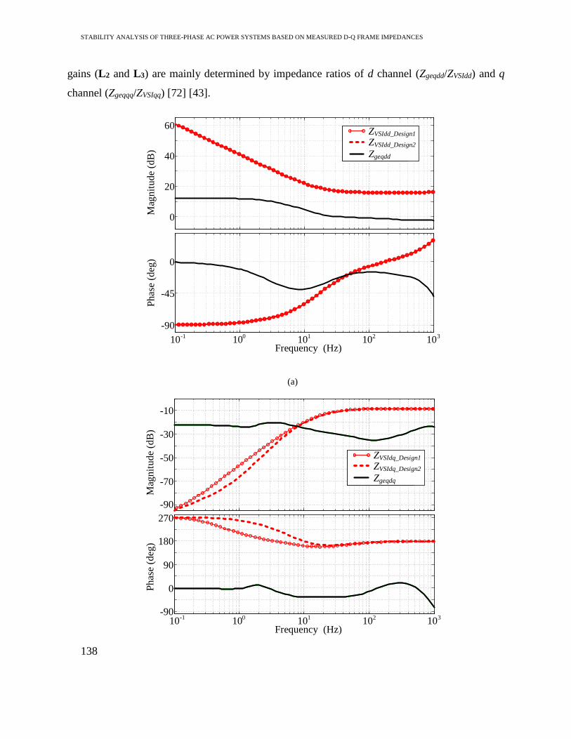
STABILITY ANALYSIS OF THREE-PHASE AC POWER SYSTEMS BASED ON MEASURED D-Q FRAME IMPEDANCES
138
gains (L2 and L3) are mainly determined by impedance ratios of d channel (Zgeqdd/ZVSIdd) and q
channel (Zgeqqq/ZVSIqq) [72] [43].
0
20
40
60
-90
-45
0
Frequency (Hz)10
-110
010
110
210
3
Mag
nit
ude
(dB
)P
has
e (d
eg)
ZVSIdd_Design1
ZVSIdd_Design2
Zgeqdd
(a)
-90
-70
-50
-30
-10
-90
0
90
180
270
Frequency (Hz)10
-110
010
110
210
3
Mag
nit
ude
(dB
)P
has
e (d
eg)
ZVSIdq_Design1
ZVSIdq_Design2
Zgeqdq
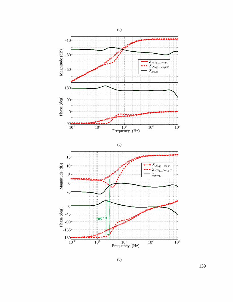
139
(b)
-50
-30
-10
-90
0
90
180
Frequency (Hz)10
-110
010
110
210
3
Mag
nit
ud
e (d
B)
Ph
ase
(deg
)ZVSIqd_Design1
ZVSIqd_Design2
Zgeqqd
(c)
-5
0
5
10
15
Mag
nit
ude
(dB
)
-180
-135
-90
-45
0
Phas
e (d
eg)
Frequency (Hz)10
-110
010
110
210
3
ZVSIqq_Design1
ZVSIqq_Design2
Zgeqqq
185°
(d)

STABILITY ANALYSIS OF THREE-PHASE AC POWER SYSTEMS BASED ON MEASURED D-Q FRAME IMPEDANCES
140
Fig. 5-12. Grid and VSI impedances for PLL Design 1 and Design 2.
Real Axis
Imag
inar
y A
xis
-50 0 50 100 150 200 250
-20
-10
0
10
20
Poles of ZVSIqq
introduced by PLL
Pole of ZVSIdd introduced
by current d channel loop
Design 1 Design 2
ZVSIdq
Zgeqdq
Fig. 5-13. Pole-zero map of VSI (ZVSIdq) and grid side impedances (Zgeqdq).
Before applying GNC to study the stability of the system, it is necessary to check the poles
and zeros of grid and VSI impedances, since stability condition of the system also rely on the
number of poles and zeros on the right-half plane (RHP).
Fig. 5-13 is the pole-zero map of VSI and grid side impedances, which shows that there is no
pole and zero of grid side impedance (Zgeqdq) locates on RHP. For VSI impedances, there is one
pole at the origin and one pole on the positive real axis. The pole at the origin is introduced by
the d channel current feedback control. Reflecting to the Bode plot of ZVSIdd, this pole gives
20dB/dec decreasing of magnitude and -90° phase (see Fig. 5-12 (a)). PLL of VSI introduces the
pole on the positive real axis. Reflecting to the Bode plot of ZVSIqq, this pole makes the magnitude
decreasing while the phase increasing at the low frequency range (see Fig. 5-12 (d)).
As discussed before, the condition for system stability can be determined by applying GNC or
GINC to the minor loop gain L2 and L3. For L2, which is defined by geqdq
Z and 1
VSIdqZ
, it is easier
to test stability by applying GNC rather than GINC. Because there is no pole from Zgeqdq locates
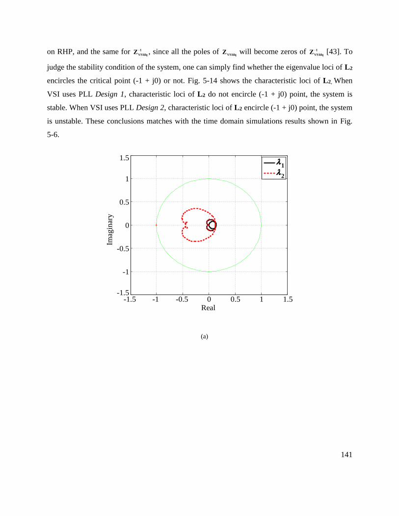
141
on RHP, and the same for 1
VSIdqZ
, since all the poles of VSIdq
Z will become zeros of 1
VSIdqZ
[43]. To
judge the stability condition of the system, one can simply find whether the eigenvalue loci of L2
encircles the critical point (-1 + j0) or not. Fig. 5-14 shows the characteristic loci of L2, When
VSI uses PLL Design 1, characteristic loci of L2 do not encircle (-1 + j0) point, the system is
stable. When VSI uses PLL Design 2, characteristic loci of L2 encircle (-1 + j0) point, the system
is unstable. These conclusions matches with the time domain simulations results shown in Fig.
5-6.
-1.5 -1 -0.5 0 0.5 1 1.5-1.5
-1
-0.5
0
0.5
1
1.5
1
2
Real
Imag
inar
y
(a)
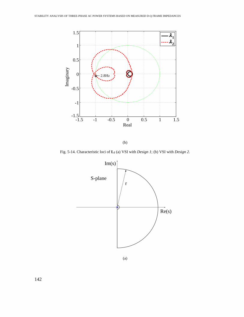
STABILITY ANALYSIS OF THREE-PHASE AC POWER SYSTEMS BASED ON MEASURED D-Q FRAME IMPEDANCES
142
-1.5 -1 -0.5 0 0.5 1 1.5-1.5
-1
-0.5
0
0.5
1
1.5
1
2
Real
Imag
inar
y
2.8Hz
(b)
Fig. 5-14. Characteristic loci of L2 (a) VSI with Design 1; (b) VSI with Design 2.
Re(s)
Im(s)
rS-plane
(a)
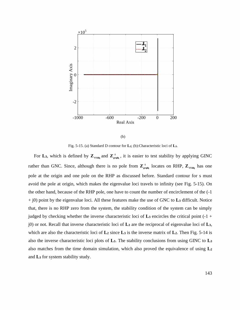
143
-1000 -600 -200 0 200
-2
0
2
Real Axis
Imag
inar
y A
xis
×105
12
(b)
Fig. 5-15. (a) Standard D contour for L3; (b):Characteristic loci of L3.
For L3, which is defined by VSIdq
Z and 1
geqdqZ
, it is easier to test stability by applying GINC
rather than GNC. Since, although there is no pole from 1
geqdqZ
locates on RHP,
VSIdqZ has one
pole at the origin and one pole on the RHP as discussed before. Standard contour for s must
avoid the pole at origin, which makes the eigenvalue loci travels to infinity (see Fig. 5-15). On
the other hand, because of the RHP pole, one have to count the number of encirclement of the (-1
+ j0) point by the eigenvalue loci. All these features make the use of GNC to L3 difficult. Notice
that, there is no RHP zero from the system, the stability condition of the system can be simply
judged by checking whether the inverse characteristic loci of L3 encircles the critical point (-1 +
j0) or not. Recall that inverse characteristic loci of L3 are the reciprocal of eigenvalue loci of L3,
which are also the characteristic loci of L2 since L3 is the inverse matrix of L2. Then Fig. 5-14 is
also the inverse characteristic loci plots of L3. The stability conclusions from using GINC to L3
also matches from the time domain simulation, which also proved the equivalence of using L2
and L3 for system stability study.

STABILITY ANALYSIS OF THREE-PHASE AC POWER SYSTEMS BASED ON MEASURED D-Q FRAME IMPEDANCES
144
5.4.3 Migration of synchronization instability
80°
0
40
80
Frequency (Hz)
-180
-135
-90
102
101
100
10-1
10-2
Mag
nit
ude
(dB
)P
has
e (d
eg)
40°
2.7 4.3
kppllVSI = 0.1
kipllVSI = 3.2
16.2
87°
Design 1kppllVSI = 0.1kipllVSI = 0.32
Design 2
kppllVSI = 0.6
kipllVSI = 3.2Design 3
Fig. 5-16. VSI PLL loop gains with different PI parameters and ideal grid.
As discussed in the stability analysis section, when VSI uses PLL Design 2, which has bigger
bandwidth and less phase margin comparing to Design 1, Zqq of VSI (ZVSIqq) and the grid (Zgeqqq)
interacts with each other and the phase difference is over 180° (see Fig. 5-12 (d)), and system is
unstable. In order to migrate the instability, one can simply reduce the PLL bandwidth and adopt
Design 1, which makes no interaction between ZVSIqq and Zgeqqq. However, instability can also be
migrated by increasing the phase margin of PLL while still keep higher bandwidth, for example
using PLL Design 3 as shown in Fig. 5-16. Fig. 5-17 (a) shows the Zqq of VSI using three PLL
designs. Same as using Design 1, ZVSIqq using PLL Design 3 do not interact with the grid side
impedance. Fig. 5-17 (b) shows the characteristic loci of L2 when VSI uses PLL Design 3, which
indicate the system is stable with VSI using PLL Design 3. Simulation results in time domain
shown in Fig. 5-18 also verify the conclusion.

145
-5
0
5
10
15
Mag
nit
ude
(dB
)
-180
-135
-90
-45
0
Phas
e (d
eg)
Frequency (Hz)10
-110
010
110
210
3
kppllVSI = 0.1
kipllVSI = 3.2
kppllVSI = 0.1
kipllVSI = 0.32
kppllVSI = 0.6
kipllVSI = 3.2
Design 1
Design 2
Design 3
Zgeqqq
(a)
-1.5 -1 -0.5 0 0.5 1 1.5-1.5
-1
-0.5
0
0.5
1
1.5
1
2
Real
Imag
inar
y
(b)
Fig. 5-17. (a) Zqq of grid side and VSI; (b) characteristic loci of L2 with Design 3.
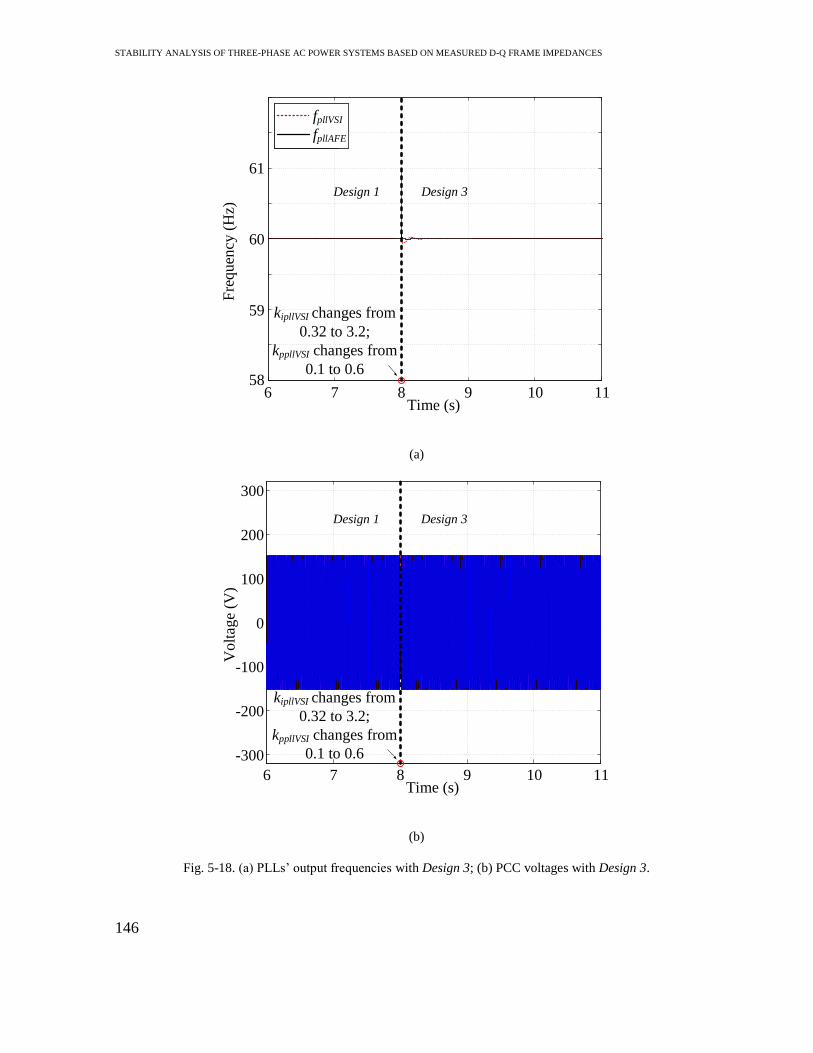
STABILITY ANALYSIS OF THREE-PHASE AC POWER SYSTEMS BASED ON MEASURED D-Q FRAME IMPEDANCES
146
6 7 8 9 10 1158
59
60
61
Time (s)
Fre
qu
ency
(H
z)
fpllVSI
fpllAFE
kipllVSI changes from
0.32 to 3.2;
kppllVSI changes from
0.1 to 0.6
Design 1 Design 3
(a)
-300
-200
-100
0
100
200
300
Volt
age
(V)
kipllVSI changes from
0.32 to 3.2;
kppllVSI changes from
0.1 to 0.6
6 7 8 9 10 11Time (s)
Design 1 Design 3
(b)
Fig. 5-18. (a) PLLs’ output frequencies with Design 3; (b) PCC voltages with Design 3.
147
VSI
AFE
Control
Board
Sensors Board
IGBT Modules
Grid Side Resistor
Passive Load
Fig. 5-19. Test-bed hardware prototype for experimental system
5.5 Experimental Results
A low power test-bed hardware prototype (Fig. 5-19) of system shown in Fig. 5-1 is built in
the laboratory to verify the proposed analysis. Table 5-2 gives the parameters of the test-bed
hardware.
In the experiment, VSI is started first, and then AFE is started. Two experiments are shown.
In the first experiment, VSI and AFE work stably with the weak grid and passive load (Fig. 5-20
(a)). In the second one, the system is unstable (Fig. 5-20 (b)). From stable to unstable test, only
PLL parameters of VSI and AFE are changed.

STABILITY ANALYSIS OF THREE-PHASE AC POWER SYSTEMS BASED ON MEASURED D-Q FRAME IMPEDANCES
148
139 V 100 V
ωVSI ωAFE
VPCC
IaVSIAFE starts
(a) Stable case. VPCC [100 V/DIV], IaVSI [10 A/DIV], ωVSI, ωAFE [0.05 Hz/DIV]
2 s
ωVSI ωAFE
VPCC
IaVSI
AFE starts
(b) Unstable case. VPCC [100 V/DIV], IaVSI [10 A/DIV], ωVSI, ωAFE [0.05 Hz/DIV]
Fig. 5-20. Experimental test results.
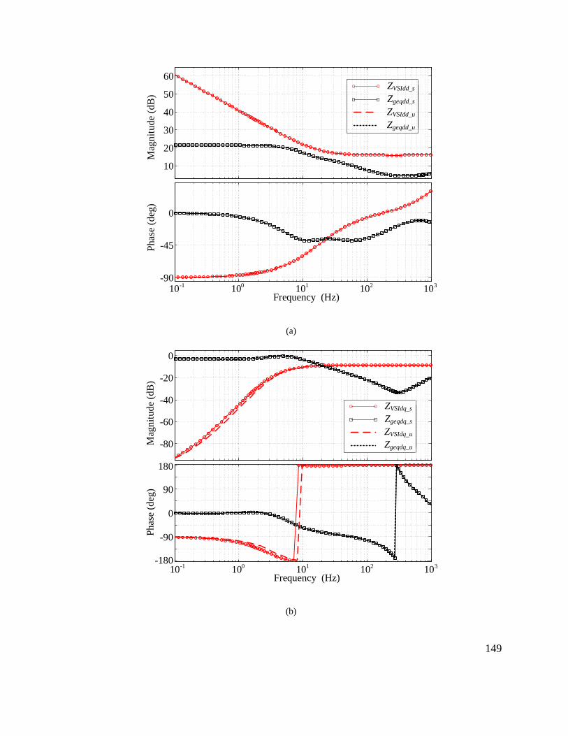
149
ZVSIdd_s
Zgeqdd_s
ZVSIdd_u
Zgeqdd_u
10
20
30
40
50
60
-90
-45
0
Mag
nit
ude
(dB
)P
has
e (d
eg)
Frequency (Hz)10
-110
010
110
210
3
(a)
-80
-60
-40
-20
0
-180
-90
0
90
180
Frequency (Hz)10
-110
010
110
210
3
Mag
nit
ude
(dB
)P
has
e (d
eg)
ZVSIdq_s
Zgeqdq_s
ZVSIdq_u
Zgeqdq_u
(b)
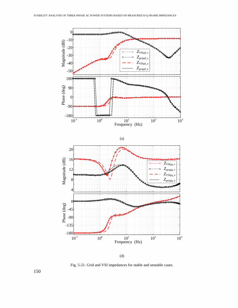
STABILITY ANALYSIS OF THREE-PHASE AC POWER SYSTEMS BASED ON MEASURED D-Q FRAME IMPEDANCES
150
-50
-40
-30
-20
-10
0
-180
-90
0
90
180
Mag
nit
ude
(dB
)P
has
e (d
eg)
Frequency (Hz)10
-110
010
110
210
3
ZVSIqd_s
Zgeqqd_s
ZVSIqd_u
Zgeqqd_u
(a)
-180
-135
-90
-45
0
4
8
12
16
20
Mag
nit
ud
e (d
B)
Ph
ase
(d
eg)
Frequency (Hz)10
-110
010
110
210
3
ZVSIqq_s
Zgeqqq_s
ZVSIqq_u
Zgeqqq_u
(d)
Fig. 5-21. Grid and VSI impedances for stable and unstable cases.

151
Using the models in section 5.4 and the parameters in Table 5-2, impedances of VSI and grid
are calculated for the experimental systems. They are shown in Fig. 5-21. As a result, the
experimental system is diagonal dominant. Because, for both VSI and grid side impedances, Zdq
and Zqd are more than 10 dB smaller compare to Zdd and Zqq. Eigenvalues of minor loop-gains
(L2 and L3) are mainly determined by impedance ratios of d channel (Zgeqdd/ZVSIdd) and q channel
(Zgeqqq/ZVSIqq), Zdq and Zqd can be ignored. Changes of PLL parameters changes Zqq. As Fig. 5-22
shows, although for both stable and unstable condition, ZVSIqq interacts with Zgeqqq, stable case
has nearly 30° phase margin while the unstable case has no phase margin.
Table 5-2. Parameters of experimental system
Symbol Description Value
Vg Grid phase-neutral peak voltage 260 V
fg Grid voltage frequency 60 Hz
LVSI Inductance of inverter 1 mH
VdcVSI Inverter dc voltage 270 V
fsw Switching frequency of VSI and AFE 20 kHz
IdrefVSI d channel current of VSI 11 A
IqrefVSI q channel current of VSI 0 A
kpiVSI Proportional gain of VSI current controller 0.0233
kiiVSI Integrator gain of VSI current controller 2.560
kppllVSI Proportional gain of VSI PLL 0.1
kipllVSI Integral gain of VSI PLL 3.2 (unstable); 2 (stable)
LAFE Inductance of AFE 0.5 mH
CdcAFE Dc link capacitor of AFE 100 μF
Rdc Load resistor of AFE 96 Ω
VdcAFE Dc voltage of AFE 231 V
kpiAFE Proportional gain of AFE current controller 0.0116
kiiAFE Integrator gain of AFE current controller 2.5598
kpvAFE Proportional gain of AFE voltage controller 0.0628
kivAFE Integrator gain of AFE voltage controller 6.9813

STABILITY ANALYSIS OF THREE-PHASE AC POWER SYSTEMS BASED ON MEASURED D-Q FRAME IMPEDANCES
152
kppllAFE Proportional gain of AFE PLL 0.2 (unstable); 0.3 (stable)
kipllAFE Integral gain AFE of PLL 1
ZL Local passive load RLoad: 10 Ω; CLoad: 50 μF
Zg Grid impedance 10 Ω
8
10
12
14
16
18
Mag
nit
ude
(dB
)
1-180
-90
0
Phas
e (d
eg)
Frequency (Hz)2 3 4
180.1°157°
ZVSIqq_s
Zgeqqq_s
ZVSIqq_u
Zgeqqq_u
Fig. 5-22. Zqq of grid and VSI for stable and unstable cases.
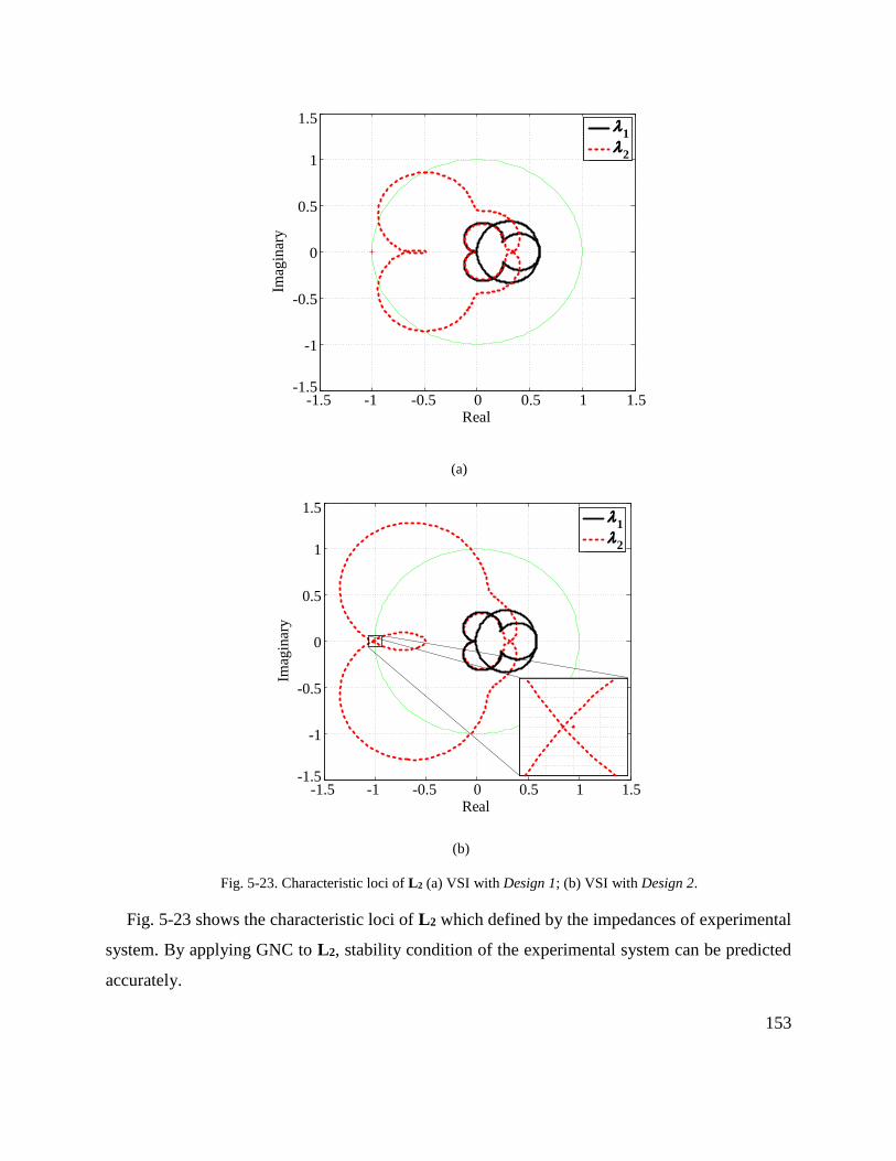
153
-1.5 -1 -0.5 0 0.5 1 1.5-1.5
-1
-0.5
0
0.5
1
1.5
1
2
Real
Imag
inar
y
(a)
-1.5 -1 -0.5 0 0.5 1 1.5-1.5
-1
-0.5
0
0.5
1
1.5
Real
Imag
inar
y
1
2
(b)
Fig. 5-23. Characteristic loci of L2 (a) VSI with Design 1; (b) VSI with Design 2.
Fig. 5-23 shows the characteristic loci of L2 which defined by the impedances of experimental
system. By applying GNC to L2, stability condition of the experimental system can be predicted
accurately.

STABILITY ANALYSIS OF THREE-PHASE AC POWER SYSTEMS BASED ON MEASURED D-Q FRAME IMPEDANCES
154
This paper proposes an impedance-based analysis method to analyze the grid-synchronization
stability issue in paralleled three-phase converter systems including grid-tied inverter, active
front end rectifier, local passive load, and grid impedance. The proposed method shows that the
multi-variable generalized Nyquist stability criterion (GNC) and generalized inverse Nyquist
stability criterion (GINC) can be used to predict the system stability based on the grid and
inverter impedances in the synchronous d-q frame. Furthermore, the instability is found to be
caused by qq channel impedance interaction. Experimental results verify the analysis and the
proposed method.

155
Chapter 6 Impedance-based Analysis of Islanding Dection for
Grid-tied Inverter Systems
Islanding detection is an important function of distributed generation units because of the
requirement of grid code compliance [96]. On the other hand, islanding detection function gives
distributed generation unit the capability of adjusting its operation mode according to grid
condition. For example, the three-phase inverter, as shown in Fig. 6-1, can work as a current
source when it is connected to the grid. It can work as a voltage source to feed the local load
(islanding mode) when it is disconnected with grid because of grid faults.
Many islanding detection methods have been developed. Methods that rely on monitoring the
changes of grid parameters are defined as passive methods. For example, over/under voltage or
frequency detection. Methods generate small perturbations to force the change of grid parameters
are defined as active methods. For example, active frequency drift (AFD) islanding detection
method forces frequency drifts enough to activate over/under frequency protection when
islanding condition happens. Other active methods include grid impedance estimation and
negative sequence detection [90]. Among them, AFD methods are popular because of their
simplicity, small non-detection zone, and low impact on system power quality. Most AFD
methods generate a frequency positive feedback, such as the Sandia frequency shift (SFS)
method, which drives the converter system frequency away from the steady-state and detects the
islanding event [97]–[101]. Other methods are based on the analysis of PLL small-signal stability
[102].
Different from traditional analysis of AFD method, this paper proposes an impedance-based
analysis which unveils that frequency drift is the consequence of interaction between inverter
output impedance and the impedance of local loads. Moreover, impedance-based analysis also
shows that, AFD method has the potential to destabilize the grid-connected inverter system when
the grid is week or the size of inverter is large.
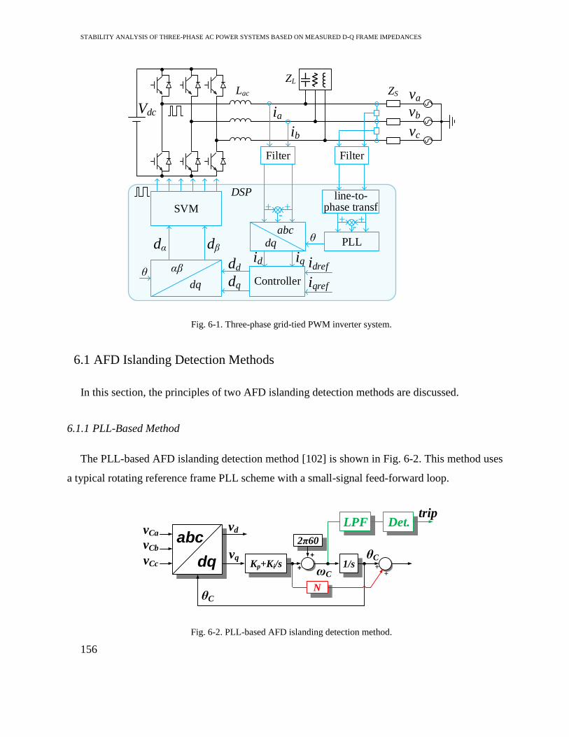
STABILITY ANALYSIS OF THREE-PHASE AC POWER SYSTEMS BASED ON MEASURED D-Q FRAME IMPEDANCES
156
Vdc
line-to- phase transf
dqabc
Controller
PLL
id iq idref
iqref
θ
SVM
dq
αβ dd
dq
dα dβ
θ
DSP
Filter
ia
ib
va
vb
vc
+-+
+-+
Lac
Filter
ZL
ZS
Fig. 6-1. Three-phase grid-tied PWM inverter system.
6.1 AFD Islanding Detection Methods
In this section, the principles of two AFD islanding detection methods are discussed.
6.1.1 PLL-Based Method
The PLL-based AFD islanding detection method [102] is shown in Fig. 6-2. This method uses
a typical rotating reference frame PLL scheme with a small-signal feed-forward loop.
dq
abc
Kp+Ki/s 1/s
2π60
vq
vd
vCb
vCc
vCa
θC +
ωC
LPF Det.trip
N
+ ++
θC
Fig. 6-2. PLL-based AFD islanding detection method.
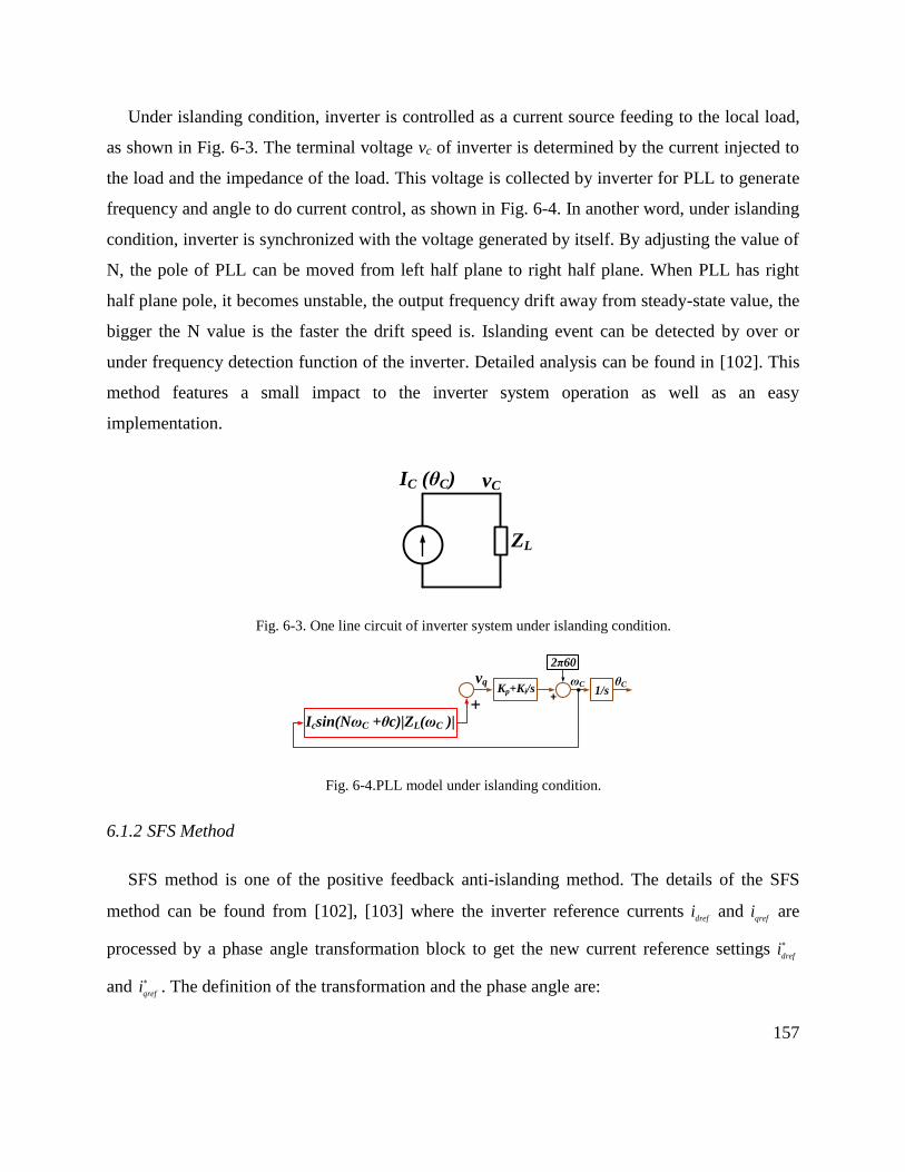
157
Under islanding condition, inverter is controlled as a current source feeding to the local load,
as shown in Fig. 6-3. The terminal voltage vc of inverter is determined by the current injected to
the load and the impedance of the load. This voltage is collected by inverter for PLL to generate
frequency and angle to do current control, as shown in Fig. 6-4. In another word, under islanding
condition, inverter is synchronized with the voltage generated by itself. By adjusting the value of
N, the pole of PLL can be moved from left half plane to right half plane. When PLL has right
half plane pole, it becomes unstable, the output frequency drift away from steady-state value, the
bigger the N value is the faster the drift speed is. Islanding event can be detected by over or
under frequency detection function of the inverter. Detailed analysis can be found in [102]. This
method features a small impact to the inverter system operation as well as an easy
implementation.
ZL
IC (θC) vC
Fig. 6-3. One line circuit of inverter system under islanding condition.
Kp+Ki/s 1/svq ωC θC
Icsin(NωC +θc)|ZL(ωC )|+
+
2π60
Fig. 6-4.PLL model under islanding condition.
6.1.2 SFS Method
SFS method is one of the positive feedback anti-islanding method. The details of the SFS
method can be found from [102], [103] where the inverter reference currents dref
i and qref
i are
processed by a phase angle transformation block to get the new current reference settings
drefi
and
qrefi . The definition of the transformation and the phase angle are:
STABILITY ANALYSIS OF THREE-PHASE AC POWER SYSTEMS BASED ON MEASURED D-Q FRAME IMPEDANCES
158
qref
dref
ff
ff
qref
dref
i
i
i
i
cossin
sincos
(6-1)
00
2
Kcf
f
(6-2)
The angle f
used in the transformation block is calculated from the SFS control, in which
is the inverter terminal voltage frequency, 0
is the grid nominal frequency, K is the positive
feedback gain, and 0
cf is the initial chopping factor. [9]
Positive feedback always tries to perturb the grid-tied inverter system. When the grid is
connected, the system is operated stably. However, when islanding event happens, the system is
destabilized so that the frequency drift detection unit is tripped.
6.2 Impedance-Based Analysis of Inverter System AFD Methods
Unlike most analyses for AFD islanding detection methods, this paper presents an impedance-
based analysis which uses the terminal characteristics of inverter and loads. The advantages of
impedance-based analysis is that impedance can be measured, no internal parameters of the
inverter are need, and it is easier to address compatibility issue between inverter and the grid by
using impedances and Nyquist stability criteria.
Grid-tied inverter can be modeled as a voltage source in series with an output impedance as
shown in Fig. 6-5. Impedance-based analysis studies the islanding event by the interaction
between the output impedance of inverter and the input impedance of local load. When the
system is connected to the grid, the grid impedance should be considered too; for a stiff grid, the
impedance is small, for a weak grid, the impedance is big.
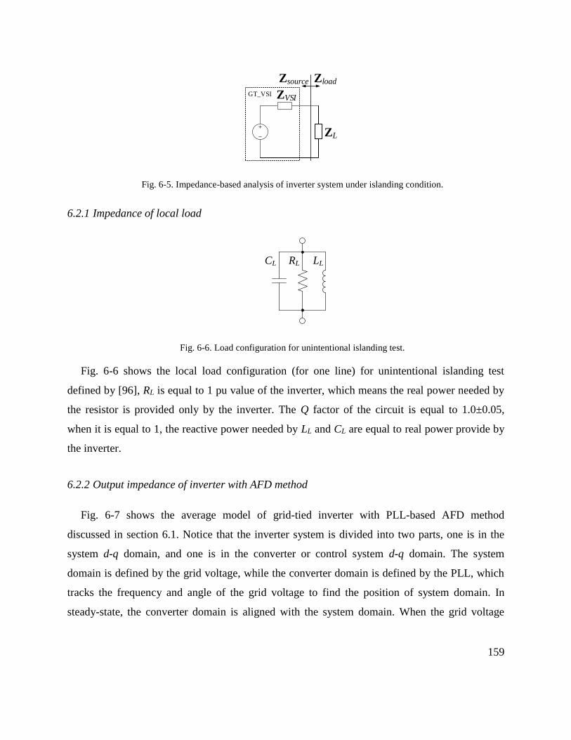
159
ZL
ZVSIGT_VSI
Zsource Zload
Fig. 6-5. Impedance-based analysis of inverter system under islanding condition.
6.2.1 Impedance of local load
CL RL LL
Fig. 6-6. Load configuration for unintentional islanding test.
Fig. 6-6 shows the local load configuration (for one line) for unintentional islanding test
defined by [96], RL is equal to 1 pu value of the inverter, which means the real power needed by
the resistor is provided only by the inverter. The Q factor of the circuit is equal to 1.0±0.05,
when it is equal to 1, the reactive power needed by LL and CL are equal to real power provide by
the inverter.
6.2.2 Output impedance of inverter with AFD method
Fig. 6-7 shows the average model of grid-tied inverter with PLL-based AFD method
discussed in section 6.1. Notice that the inverter system is divided into two parts, one is in the
system d-q domain, and one is in the converter or control system d-q domain. The system
domain is defined by the grid voltage, while the converter domain is defined by the PLL, which
tracks the frequency and angle of the grid voltage to find the position of system domain. In
steady-state, the converter domain is aligned with the system domain. When the grid voltage

STABILITY ANALYSIS OF THREE-PHASE AC POWER SYSTEMS BASED ON MEASURED D-Q FRAME IMPEDANCES
160
contains small-signal perturbations, which means the system domain is changing, the converter
domain is no longer aligned with the system domain because of the PLL dynamics (PI of PLL).
In effect, small-signal perturbations of the system voltage propagate to the PLL output angle,
and further to the converter domain current. Through the current controller, the perturbation
propagates to the duty ratio and the voltage generated by the inverter power stage and finally to
the output current of the inverter. This analysis indicates that the PLL has an impact on the
output impedance of the grid-tied inverter.
average model of power
stage in system d-q domain
converter d-q domain
idc
3L 3RL
3L 3RLidL
s sdd iqL
sdq
s
dqvdcs
dds
vdc
vqs
vds
PI
dds
vqc
dqs
vds
vqs
dq frame
controller
1/s
-1
idLrefs
siqLref
+-
+-
vdc
3ωLiqLs
3ωLidLs
idLs
iqLs
idLc
iqLc
idLs
iqLs
N++
Small signal propagation path Zout
Fig. 6-7. Average model of grid-tied inverter with AFD method.
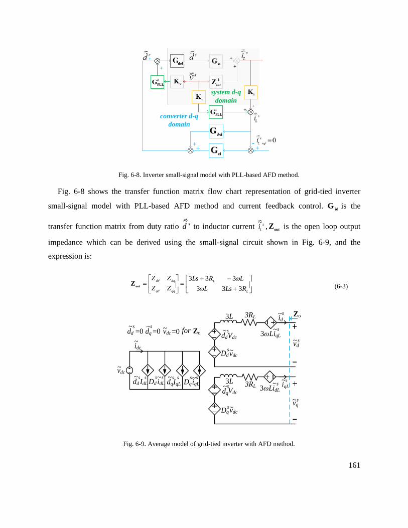
161
+
++
+
+
+
+-
++
system d-q
domain
converter d-q
domain
Fig. 6-8. Inverter small-signal model with PLL-based AFD method.
Fig. 6-8 shows the transfer function matrix flow chart representation of grid-tied inverter
small-signal model with PLL-based AFD method and current feedback control. id
G is the
transfer function matrix from duty ratio sd
~
to inductor current s
Li~
,out
Z is the open loop output
impedance which can be derived using the small-signal circuit shown in Fig. 6-9, and the
expression is:
L
L
qqqd
dqdd
RLsL
LRLs
ZZ
ZZ
333
333
out
Z (6-3)
3L
3L
vdc~
idc~
~ ~
3RL
3RLIdL
sdd
sDd
sidL
sdq
~sIqL
sDq
siqL~s
Dqsvdc~
dqVdc~s
ddVdc
~s
Dd vdc~s
3ωLiqL~s
id~s
3ωLidL~s iqL
~s
vq~s
vd~ s
Zo
vdc~ =0dq
~s
=0dd
~s=0 Zofor
Fig. 6-9. Average model of grid-tied inverter with AFD method.
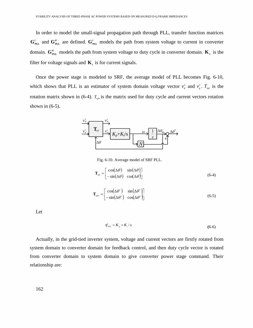
STABILITY ANALYSIS OF THREE-PHASE AC POWER SYSTEMS BASED ON MEASURED D-Q FRAME IMPEDANCES
162
In order to model the small-signal propagation path through PLL, transfer function matrices
i
PLLG and
d
PLLG are defined.
i
PLLG models the path from system voltage to current in converter
domain. d
PLLG models the path from system voltage to duty cycle in converter domain.
vK is the
filter for voltage signals and i
K is for current signals.
Once the power stage is modeled to SRF, the average model of PLL becomes Fig. 6-10,
which shows that PLL is an estimator of system domain voltage vector s
dv and
s
qv .
T is the
rotation matrix shown in (6-4).
T is the matrix used for duty cycle and current vectors rotation
shown in (6-5).
Kp+Ki/s
Δθ
Δθ TΔθ
v sd
v sq
v cd
v cq ω
N+
+ Δθ*
Fig. 6-10. Average model of SRF PLL.
cossin
sincosT
(6-4)
cossin
sincosT
(6-5)
Let
sKKtfipPLL/
(6-6)
Actually, in the grid-tied inverter system, voltage and current vectors are firstly rotated from
system domain to converter domain for feedback control, and then duty cycle vector is rotated
from converter domain to system domain to give converter power stage command. Their
relationship are:

163
sc DD
*T , sc VV
T , sc II
* T (6-7)
Under steady state the angle between vectors in two domains is zero:
sc DD
)0cos()0sin(
)0sin()0cos( (6-8)
Small signal perturbation can be added to (6-8) to get:
s
q
s
q
s
d
s
d
c
q
c
q
c
d
c
d
dD
dD
dD
dD~
~
)~
0cos()~
0sin(
)~
0sin()~
0cos(~
~
(6-9)
By doing approximation of trigonometric functions, and cancel the steady state values.
Relationship between converter domain duty cycle and system domain duty cycle can be derived
as:
s
q
s
q
s
d
s
d
c
q
c
q
c
d
c
d
dD
dD
dD
dD~
~
1~
~1
~
~
(6-10)
s
q
s
d
s
q
s
d
c
q
c
d
dD
Dd
d
d~~
~~
~
~
(6-11)
Since,
c
qPLLvtfN ~~~ (6-12)
Then,
s
q
c
qPLL
s
d
c
qPLL
s
q
s
d
c
q
c
d
dvtfND
vtfNDd
d
d~~~
~~~
~
~
(6-13)
By doing similar small signal analysis as above for voltage vectors, relation between PLL
output angle and q axis voltage can be derive as [11]:

STABILITY ANALYSIS OF THREE-PHASE AC POWER SYSTEMS BASED ON MEASURED D-Q FRAME IMPEDANCES
164
s
q
s
d
c
qvVv ~~~ (6-14)
s
qPLL
s
q
PLL
s
d
PLL vGvtfVs
tf ~~~
(6-15)
Substitute (6-14) and (6-15) to (6-13):
s
q
s
d
PLLPLL
s
dPLL
s
d
PLLPLL
s
dPLL
s
q
s
q
s
d
c
q
c
d
v
v
NtfGVNtfD
NtfGVNtfD
d
d
d
d~
~
10
10~
~
~
~
(6-16)
Then:
PLLPLL
s
dPLL
s
d
PLLPLL
s
dPLL
s
q
NtfGVNtfD
NtfGVNtfD
10
10d
PLLG (6-17)
Using similar approach, i
PLLG can be derived as:
PLLPLL
s
dPLL
s
d
PLLPLL
s
dPLL
s
q
NtfGVNtfI
NtfGVNtfI
10
10i
PLLG (6-18)
Solving the equations represented by Fig. 6-8, the output impedance of grid-tied inverter
system with PLL-based AFD is:
ideicidelid
1
v
d
PLL
i
PLLdeicidelid
1
outout_il_PLL
KGGGGI
KGGGGGGZZ
(6-19)
Table 6-1. Parameters for simulation and Calculation
Symbol Description Value
Vdc (V) Dc voltage 270
Vsd (V) D channel source voltage 99.6
Vsq (V) Q channel source voltage 0
f (Hz) Line frequency 60

165
Lac (mH) Ac inductor 1
RLac (mΩ) Ac inductor ESR 110
Idref (A) D channel current reference -10
Iqref (A) Q channel current reference 0
Kpi Current controller proportional gain 0.0233
Kii Current controller integral gain 2.5598
Kp PLL proportional gain 1
Ki PLL integral gain 2
fsw (kHz) Switching frequency 20
RL (Ω) Load resistor 10
LL (mH) Load inductor 17.4
CL (µF) Load capacitor 400
Using the parameters in Table 6-1, Fig. 6-11 shows the Bode plot of grid-tied inverter output
impedance. The results shows that the q-q channel dc impedance is a negative incremental
resistance. The magnitude of Zqq equals to the per unit value of inverter system. A higher power
rating of the inverter will result in a lower magnitude negative resistance as shown in the Zqq.
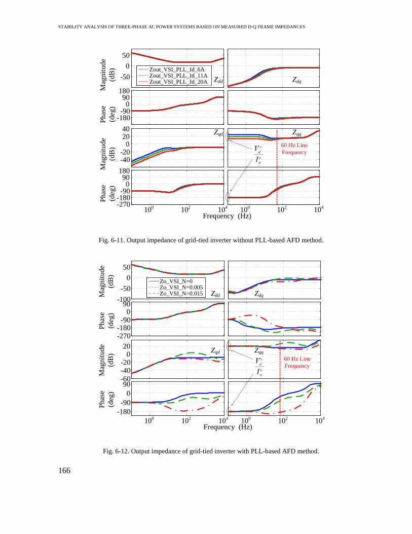
STABILITY ANALYSIS OF THREE-PHASE AC POWER SYSTEMS BASED ON MEASURED D-Q FRAME IMPEDANCES
166
-50
0
50
-180-90
090
180
-40-20
02040
-270-180-90
090
180
Zout_VSI_PLL_Id_6AZout_VSI_PLL_Id_11AZout_VSI_PLL_Id_20A
Frequency (Hz)10
010
210
410
010
210
4
Mag
nit
ud
e
(dB
)
Ph
ase
(deg
)
Mag
nit
ud
e
(dB
)
Ph
ase
(deg
)
Zdd Zdq
Zqd Zqq
60 Hz Line
Frequency
Fig. 6-11. Output impedance of grid-tied inverter without PLL-based AFD method.
Zdd Zdq
Zqd Zqq
-100
-50
0
50
-270-180-90
090
-60-40-20
020
-180
-90
0
90
Zo_VSI_N=0Zo_VSI_N=0.005Zo_VSI_N=0.015
Frequency (Hz)
Mag
nit
ud
e
(dB
)
Ph
ase
(deg
)
Mag
nit
ud
e
(dB
)
Ph
ase
(deg
)
100
102
104
100
102
104
60 Hz Line
Frequency
Fig. 6-12. Output impedance of grid-tied inverter with PLL-based AFD method.

167
Fig. 6-12 shows the output impedance of the grid-tied inverter with different feed forward
gain N in the PLL-based AFD method. Because of the feed forward loop, the phase of Zqq drops
below -180°. The bigger feed forward gain is, the lower the phase of Zqq is.
-50
0
50
-900
90180270
-40
-20
0
20
-180-90
090
180
Zo_VSI_K=0Zo_VSI_K=0.005Zo_VSI_K=0.015
Frequency (Hz)10
010
210
410
010
210
4
60 Hz Line
Frequency
Mag
nit
ud
e
(dB
)
Ph
ase
(deg
)
Mag
nit
ud
e
(dB
)
Ph
ase
(deg
)
Fig. 6-13. Output impedance of grid-tied inverter with SFS AFD method.
Fig. 6-13 shows the output impedance of the grid-tied inverter with different positive
feedback gain K in the SFS AFD method. Similar phenomenon can be found that the phase of Zqq
drops below -180°. The bigger positive feedback gain K is, the lower the phase of Zqq is.
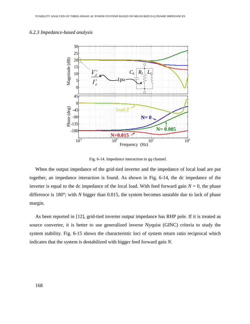
STABILITY ANALYSIS OF THREE-PHASE AC POWER SYSTEMS BASED ON MEASURED D-Q FRAME IMPEDANCES
168
6.2.3 Impedance-based analysis
0
5
10
15
20
25
30
Mag
nit
ud
e (d
B)
-180
-135
-90
-45
0
45
Ph
ase
(deg
)
Frequency (Hz)10
-110
010
110
2
N= 0
N=0.015
N= 0.005
load Z
1pu
CL RL LL
Fig. 6-14. Impedance interaction in qq channel.
When the output impedance of the grid-tied inverter and the impedance of local load are put
together, an impedance interaction is found. As shown in Fig. 6-14, the dc impedance of the
inverter is equal to the dc impedance of the local load. With feed forward gain N = 0, the phase
difference is 180°; with N bigger than 0.015, the system becomes unstable due to lack of phase
margin.
As been reported in [12], grid-tied inverter output impedance has RHP pole. If it is treated as
source converter, it is better to use generalized inverse Nyquist (GINC) criteria to study the
system stability. Fig. 6-15 shows the characteristic loci of system return ratio reciprocal which
indicates that the system is destabilized with bigger feed forward gain N.

169
Imag
inar
y
Real
N= 0
N= 0.005
N= 0.015
0.04
0.03
0.02
0.01
0
-0.01
-1 0.99-1.01
Fig. 6-15. Characteristic loci of inverter system.
6.3 Experimental Results of Islanding Detection
In order to verify the proposed model and analysis, output impedances of a three-phase grid-
tied inverter with PLL-based and SFS AFD islanding detection methods are measured with
different parameters which is listed in Table 6-2. According to the analysis above, the critical
dynamics locates at low frequency range (0.1~10Hz) which the impedance analyzer [13] in the
lab cannot measure. In order to show the interesting dynamics, the line frequency is changed to
400 Hz, the bandwidth of PLL is also increased as shown in Table 6-2.
Table 6-2. Parameters for Experimental Verification
Symbol Description Value
f (Hz) Line frequency 400
Kp PLL proportional gain 8.921
Ki PLL integral gain 3964

STABILITY ANALYSIS OF THREE-PHASE AC POWER SYSTEMS BASED ON MEASURED D-Q FRAME IMPEDANCES
170
Fig. 6-16 shows the comparison between measurement results and model calculation results
for Zqq of grid-tied inverter with and without PLL-based AFD method. Fig. 6-17 shows the
corresponding comparison for SFS AFD method.
Zqq_normal_expZqq_normal_calZqq_PLL_AFD_expZqq_PLL_AFD_cal
15
20
25
30
35
-180-135-90-45
04590
135
Mag
nit
ude
(dB
)P
has
e (d
eg)
Frequency (Hz)101 102 103 104
400 Hz Line Frequency
Fig. 6-16 Measurement of Zqq for PLL-based AFD method with N = 0.0005.
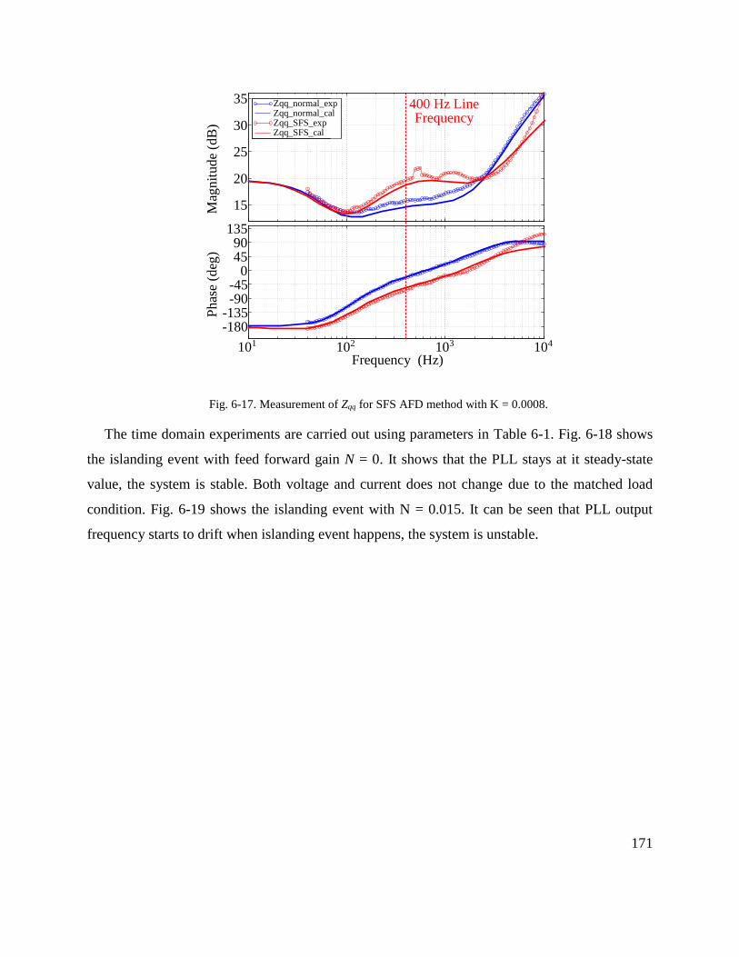
171
15
20
25
30
35
-180-135-90-45
04590
135
Zqq_normal_expZqq_normal_calZqq_SFS_expZqq_SFS_cal
Mag
nit
ud
e (d
B)
Ph
ase
(deg
)
Frequency (Hz)101 102 103 104
400 Hz Line Frequency
Fig. 6-17. Measurement of Zqq for SFS AFD method with K = 0.0008.
The time domain experiments are carried out using parameters in Table 6-1. Fig. 6-18 shows
the islanding event with feed forward gain N = 0. It shows that the PLL stays at it steady-state
value, the system is stable. Both voltage and current does not change due to the matched load
condition. Fig. 6-19 shows the islanding event with N = 0.015. It can be seen that PLL output
frequency starts to drift when islanding event happens, the system is unstable.

STABILITY ANALYSIS OF THREE-PHASE AC POWER SYSTEMS BASED ON MEASURED D-Q FRAME IMPEDANCES
172
Terminal voltage (purple) [100 V/DIV], inverter current (blue) [20A/DIV], ωc (green) [5 Hz/DIV]
Fig. 6-18. Islanding event (PLL with feed forward gain N = 0).
Terminal voltage (purple) [100 V/DIV], inverter current (blue) [20A/DIV], ωc (green) [5 Hz/DIV]
Fig. 6-19. PLL with feed forward gain N = 0.015 when islanding event happens.
173
Chapter 7 Impedances Specification for Balanced Distributed
Power Systems
7.1 Introduction
Although many results demonstrate the stability at the ac interface can be easily and readily
predicted using the measured impedances and the GNC in d-q frame for ac system, similar load
impedances specifications, as they are done in dc system (see Section 1.1.1 in Chapter 1), is not
reported. To fill this gap, this chapter discusses the challenges of stability analysis and load
impedance specification in three-phase ac system, namely its coupled multi-input multi-output
(MIMO) nature. Then a method to do load impedance specification in d-q frame is proposed.
Condition and limitation of the proposed method are discussed. Simulation and measurement
verify the analysis.
7.2 Ac System Small-Signal Stability Analysis in d-q Frame
Small-signal stability analysis for three-phase ac system can be analyzed in d-q frame by
applying GNC or GINC to the minor loop-gain sL as defined by Eq. (7-1). The stability
condition of the system under study is deterimined by eigenvalues of sL as shown in Eq. (7-3).
sYsY
sYsY
sZsZ
sZsZsss
lqqlqd
ldqldd
sqqsqd
sdqsdd)(
ldqsdqYZL (7-1)
sYsZsYsZsYsZsYsZ
sYsZsYsZsYsZsYsZs
lqqsqqldqsqdlqdsqqlddsqd
lqqsdqldqsddlqdsdqlddsdd)(L (7-2)
)(0
0)()()(
2
11
s
ssss
CLC (7-3)
It seems the method of using of GNC in d-q frame to study small-signal stability of three-
phase ac system is a dualism of the one for dc system. However, the essential difference between
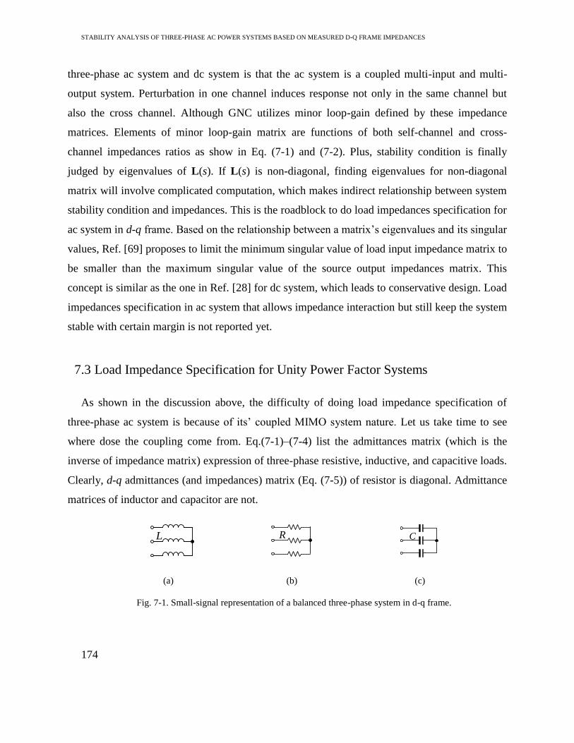
STABILITY ANALYSIS OF THREE-PHASE AC POWER SYSTEMS BASED ON MEASURED D-Q FRAME IMPEDANCES
174
three-phase ac system and dc system is that the ac system is a coupled multi-input and multi-
output system. Perturbation in one channel induces response not only in the same channel but
also the cross channel. Although GNC utilizes minor loop-gain defined by these impedance
matrices. Elements of minor loop-gain matrix are functions of both self-channel and cross-
channel impedances ratios as show in Eq. (7-1) and (7-2). Plus, stability condition is finally
judged by eigenvalues of L(s). If L(s) is non-diagonal, finding eigenvalues for non-diagonal
matrix will involve complicated computation, which makes indirect relationship between system
stability condition and impedances. This is the roadblock to do load impedances specification for
ac system in d-q frame. Based on the relationship between a matrix’s eigenvalues and its singular
values, Ref. [69] proposes to limit the minimum singular value of load input impedance matrix to
be smaller than the maximum singular value of the source output impedances matrix. This
concept is similar as the one in Ref. [28] for dc system, which leads to conservative design. Load
impedances specification in ac system that allows impedance interaction but still keep the system
stable with certain margin is not reported yet.
7.3 Load Impedance Specification for Unity Power Factor Systems
As shown in the discussion above, the difficulty of doing load impedance specification of
three-phase ac system is because of its’ coupled MIMO system nature. Let us take time to see
where dose the coupling come from. Eq.(7-1)–(7-4) list the admittances matrix (which is the
inverse of impedance matrix) expression of three-phase resistive, inductive, and capacitive loads.
Clearly, d-q admittances (and impedances) matrix (Eq. (7-5)) of resistor is diagonal. Admittance
matrices of inductor and capacitor are not.
L
R
C
(a) (b) (c)
Fig. 7-1. Small-signal representation of a balanced three-phase system in d-q frame.

175
2222
2222
LLs
s
LLs
LLsLLs
s
LdqY (7-4)
1
RdqRdqZY
1
1
1
0
0
0
0
R
R
R
R (7-5)
sCC
CsC
Cdq
Y (7-6)
7.3.1 Simplified stability analysis and load impedance specification for ac system
The structure of admittances matrix of three-phase resistor gives hint that if the source output
impedances matrix Zsdq and load admittances matrix Yldq are diagonal, then the minor loop-gain
L is diagonal as shown in Eq. (7-7), eigenvalues of L are d channel and q channel source and
load impedances ratios as shown in Eq. (7-8). System stability condition is directly judged by
source and load impedances ratios in d and q channel. Three-phase ac system becomes two
decoupled dc systems. Impedance specification methods that are developed in dc system can be
applied to these two dc systems separately. In this way, system stability are ensured with certain
GM and PM while still allows impedances interaction, which gives less conservative design
compare to the singular value based approach in Ref. [3] and [69].
sZsZ
sZsZ
sY
sY
sZ
sZsss
lqqsqq
lddsdd
lqq
ldd
sqq
sdd
1
1
0
0
0
0
0
0)(
ldqsdqYZL
(7-7)
sZsZ
sZsZ
s
ssss
lqqsqq
lddsdd
1
1
2
11
0
0
)(0
0)()()(
CLC (7-8)
The simplification shown above relies on source and load impedance matrices with diagonal
structure. Impedance matrices’ structure of typical dc-ac and ac-dc converters in ac DPS should

STABILITY ANALYSIS OF THREE-PHASE AC POWER SYSTEMS BASED ON MEASURED D-Q FRAME IMPEDANCES
176
be studied to verify this precondition. Typical dc-ac converters are voltage source inverters
(VSIs). They work as voltage source in ac DPS. Typical ac-dc converters are different rectifiers,
they work as active front-ends (AFEs) interfacing different loads or dc buses. In this paper boost
rectifier is chosen as an example.
abc
dq
dq
abc
PWM
Controller
vabc
iabc
Sampling Sampling
abc
dqVoltage
Controller
Current
Controller
Oscillator
LVSI
CVSI
RLVSI
VdcVSI
VVSIll
θ'
θ'
θ' θ'
PCC
Fig. 7-2. Power stage and control system of VSI.
7.3.2 Output impedance of VSI
VSI, as shown in Fig. 7-2, is the typical voltage source in the DPS. If output impedances of
VSIs are not designed low enough, with certain loads, the whole DPS could be unstable . In this
section, the output impedances matrix of VSI is analyzed to show that it can be shaped to be
diagonal by feedback controller. Small-signal impedance is derived by linearizing the average
model around an equilibrium point. The average model in d-q frame of VSI with feedback
controllers is shown in Fig. 7-3.

177
K Kiq
id
LVSI
iq
LVSI
id
CVSI
RLVSI
RLVSI
idddVSI ωCVSI vd
CVSI
ωCVSI vq
iqdqVSI
ZdqVVSI
ωLVSI id
ωLVSI iq
vdcVSI
dqVSI
ddVSI
Vdref
Vqref
Gdel
dqVSIddVSI
voq
vod
voq
vod
Voltage
Controller
Current
Controller
vdcVSI
vdcVSI
Fig. 7-3. Average model of VSI in d-q frame with feedback control.
As discussed in chapter 2, both power stage and the feedback controller influences the output
impedances matrix (dqvVSI
Z ). Open-loop output impedances of VSI are determined by output LC
filter and line frequency. They are independent of VSI duty-ratio steady state value (VSI
D
).
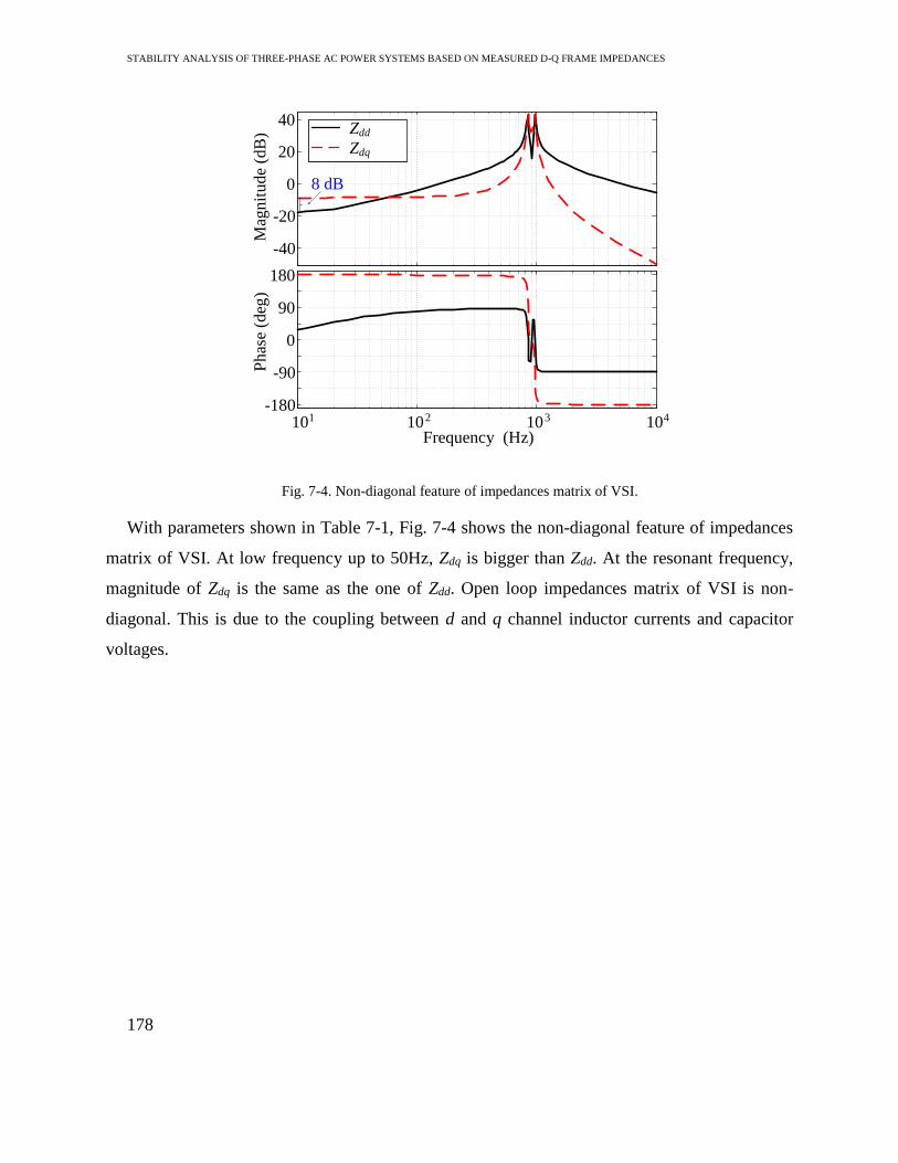
STABILITY ANALYSIS OF THREE-PHASE AC POWER SYSTEMS BASED ON MEASURED D-Q FRAME IMPEDANCES
178
-40
-20
0
20
40
-180
-90
0
90
180M
agnit
ude
(dB
)P
has
e (d
eg)
Frequency (Hz)101 102 103 104
8 dB
Zdd
Zdq
Fig. 7-4. Non-diagonal feature of impedances matrix of VSI.
With parameters shown in Table 7-1, Fig. 7-4 shows the non-diagonal feature of impedances
matrix of VSI. At low frequency up to 50Hz, Zdq is bigger than Zdd. At the resonant frequency,
magnitude of Zdq is the same as the one of Zdd. Open loop impedances matrix of VSI is non-
diagonal. This is due to the coupling between d and q channel inductor currents and capacitor
voltages.
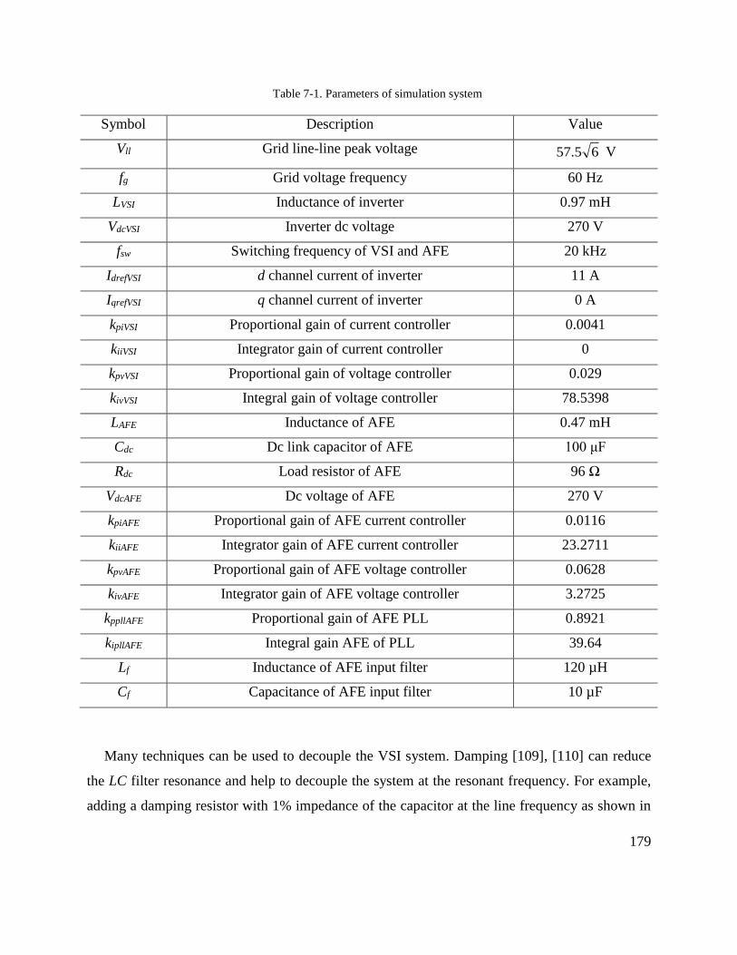
179
Table 7-1. Parameters of simulation system
Symbol Description Value
Vll Grid line-line peak voltage 65.57 V
fg Grid voltage frequency 60 Hz
LVSI Inductance of inverter 0.97 mH
VdcVSI Inverter dc voltage 270 V
fsw Switching frequency of VSI and AFE 20 kHz
IdrefVSI d channel current of inverter 11 A
IqrefVSI q channel current of inverter 0 A
kpiVSI Proportional gain of current controller 0.0041
kiiVSI Integrator gain of current controller 0
kpvVSI Proportional gain of voltage controller 0.029
kivVSI Integral gain of voltage controller 78.5398
LAFE Inductance of AFE 0.47 mH
Cdc Dc link capacitor of AFE 100 μF
Rdc Load resistor of AFE 96 Ω
VdcAFE Dc voltage of AFE 270 V
kpiAFE Proportional gain of AFE current controller 0.0116
kiiAFE Integrator gain of AFE current controller 23.2711
kpvAFE Proportional gain of AFE voltage controller 0.0628
kivAFE Integrator gain of AFE voltage controller 3.2725
kppllAFE Proportional gain of AFE PLL 0.8921
kipllAFE Integral gain AFE of PLL 39.64
Lf Inductance of AFE input filter 120 µH
Cf Capacitance of AFE input filter 10 µF
Many techniques can be used to decouple the VSI system. Damping [109], [110] can reduce
the LC filter resonance and help to decouple the system at the resonant frequency. For example,
adding a damping resistor with 1% impedance of the capacitor at the line frequency as shown in
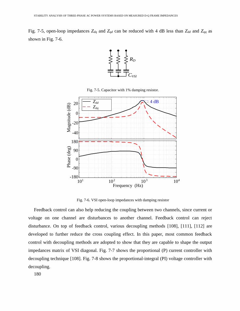
STABILITY ANALYSIS OF THREE-PHASE AC POWER SYSTEMS BASED ON MEASURED D-Q FRAME IMPEDANCES
180
Fig. 7-5, open-loop impedances Zdq and Zqd can be reduced with 4 dB less than Zdd and Zqq as
shown in Fig. 7-6.
RD
CVSI
Fig. 7-5. Capacitor with 1% damping resistor.
-40
-20
0
20
-180
-90
0
90
180
Mag
nit
ude
(dB
)P
has
e (d
eg)
Frequency (Hz)101 102 103 104
4 dBZdd
Zdq
Fig. 7-6. VSI open-loop impedances with damping resistor
Feedback control can also help reducing the coupling between two channels, since current or
voltage on one channel are disturbances to another channel. Feedback control can reject
disturbance. On top of feedback control, various decoupling methods [108], [111], [112] are
developed to further reduce the cross coupling effect. In this paper, most common feedback
control with decoupling methods are adopted to show that they are capable to shape the output
impedances matrix of VSI diagonal. Fig. 7-7 shows the proportional (P) current controller with
decoupling technique [108]. Fig. 7-8 shows the proportional-integral (PI) voltage controller with
decoupling.
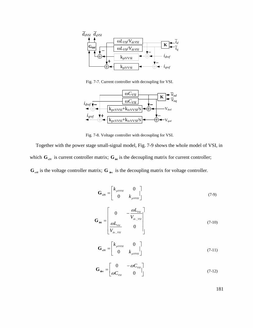
181
kpiVVSI
Kiq
id
Gdel
iqref
idref
dqVSIddVSI
ωLVSI/VdcVSI
ωLVSI/VdcVSI
kpiVVSI
Fig. 7-7. Current controller with decoupling for VSI.
K
Vdref
Vqref
voq
vod
iqref
idref
ωCVSI
ωCVSI
kpvVVSI+kivVVSI/s
kpvVVSI+kivVVSI/s
Fig. 7-8. Voltage controller with decoupling for VSI.
Together with the power stage small-signal model, Fig. 7-9 shows the whole model of VSI, in
which ciV
G is current controller matrix; dei
G is the decoupling matrix for current controller;
cvVG is the voltage controller matrix;
devG is the decoupling matrix for voltage controller.
piVVSI
piVVSI
k
k
0
0ciV
G (7-9)
0
0
_
_
VSIdc
VSI
VSIdc
VSI
V
L
V
L
deiG (7-10)
piVVSI
piVVSI
k
k
0
0ciV
G (7-11)
0
0
VSI
VSI
C
C
dev
G (7-12)
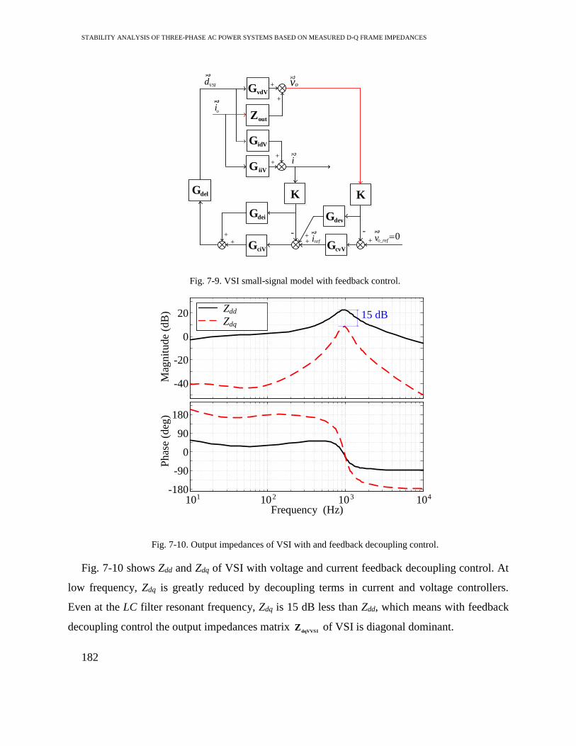
STABILITY ANALYSIS OF THREE-PHASE AC POWER SYSTEMS BASED ON MEASURED D-Q FRAME IMPEDANCES
182
+
+
++
++
+ +
-- +
dVSI
~→vo~→
io~→
i~→
GvdV
Zout
GidV
GiiV
Gdel
GciV
Gdei
i~→
ref
Gdev
GcvV
v~→
o_ref0
KK
Fig. 7-9. VSI small-signal model with feedback control.
-40
-20
0
20
-180
-90
0
90
180
Mag
nit
ud
e (d
B)
Ph
ase
(deg
)
Frequency (Hz)101 102 103 104
15 dBZdd
Zdq
Fig. 7-10. Output impedances of VSI with and feedback decoupling control.
Fig. 7-10 shows Zdd and Zdq of VSI with voltage and current feedback decoupling control. At
low frequency, Zdq is greatly reduced by decoupling terms in current and voltage controllers.
Even at the LC filter resonant frequency, Zdq is 15 dB less than Zdd, which means with feedback
decoupling control the output impedances matrix dqVVSI
Z of VSI is diagonal dominant.

183
By checking the model shown in Fig. 7-9, none of the transfer function matrices is a function
of VSI steady state values of duty-ratio (VSI
D
), output voltage (o
V
) and output current (o
I
). This
indicates that output impedances matrix dqVVSI
Z is independent of operation point of voltage-
controlled VSI (although some matrices are influenced by dcVSI
V , dcVSI
V is fixed for most of the
operation), it is only influence by power stage and feedback controllers’ parameters.
The analysis in this section can be simply concluded that output impedances matrix of VSI
can be easily shaped as diagonal dominant matrix, and it is not influenced by operation point of
VSI.
7.3.3 Admittance of AFE
Fig. 7-11 shows the power stage and control system of AFE. The power stage is a two-level
three-phase boost rectifier. PCC voltages are measured for PLL to do grid-synchronization. SRF
PLL strategy is used. Boost inductor currents and output voltages are measured by inner current
and outer voltage feedback control-loops.
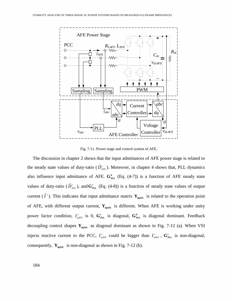
STABILITY ANALYSIS OF THREE-PHASE AC POWER SYSTEMS BASED ON MEASURED D-Q FRAME IMPEDANCES
184
AFE Power Stage
PWM
AFE Controller
PLLvdcAFE
iabc
vabc
abc
dq
Voltage
Controller
Current
Controller
LAFERLAFE
RdcCdc
θ θ
vdcAFE
iAFE
Sampling Sampling
PCC
abc
dq
Fig. 7-11. Power stage and control system of AFE.
The discussion in chapter 2 shows that the input admittances of AFE power stage is related to
the steady state values of duty-ratio ( s
AFED
). Moreover, in chapter 4 shows that, PLL dynamics
also influence input admittance of AFE. d
PLLG (Eq. (4-7)) is a function of AFE steady state
values of duty-ratio ( s
AFED
), and i
PLLG (Eq. (4-8)) is a function of steady state values of output
current ( sI
). This indicates that input admittance matrix dqAFE
Y is related to the operation point
of AFE, with different output current, dqAFE
Y is different. When AFE is working under unity
power factor condition, s
qAFEI is 0, i
PLLG is diagonal, d
PLLG is diagonal dominant. Feedback
decoupling control shapes dqAFE
Y as diagonal dominant as shown in Fig. 7-12 (a). When VSI
injects reactive current to the PCC, s
qAFEI could be bigger than s
dAFEI , i
PLLG is non-diagonal,
consequently, dqAFE
Y is non-diagonal as shown in Fig. 7-12 (b).
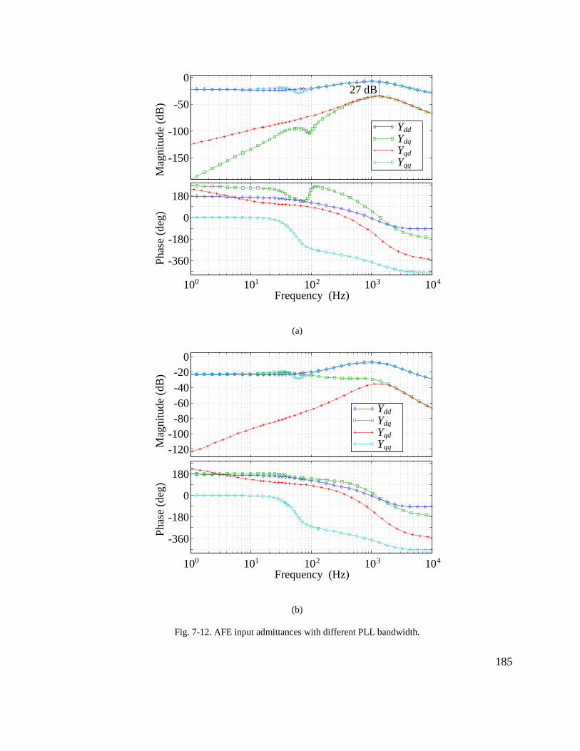
185
-360
-180
0
180
-150
-100
-50
0
27 dB
Yqq
Yqd
Ydq
Ydd
Frequency (Hz)100 101 102 103 104
Mag
nit
ud
e (d
B)
Ph
ase
(deg
)
(a)
Frequency (Hz)100 101 102 103 104
Yqq
Yqd
Ydq
Ydd
-120
-100
-80
-60
-40
-20
0
-360
-180
0
180
Mag
nit
ud
e (d
B)
Ph
ase
(deg
)
(b)
Fig. 7-12. AFE input admittances with different PLL bandwidth.
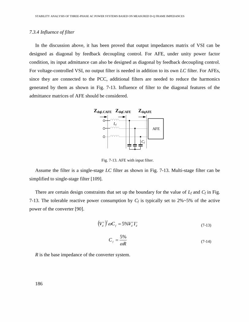
STABILITY ANALYSIS OF THREE-PHASE AC POWER SYSTEMS BASED ON MEASURED D-Q FRAME IMPEDANCES
186
7.3.4 Influence of filter
In the discussion above, it has been proved that output impedances matrix of VSI can be
designed as diagonal by feedback decoupling control. For AFE, under unity power factor
condition, its input admittance can also be designed as diagonal by feedback decoupling control.
For voltage-controlled VSI, no output filter is needed in addition to its own LC filter. For AFEs,
since they are connected to the PCC, additional filters are needed to reduce the harmonics
generated by them as shown in Fig. 7-13. Influence of filter to the diagonal features of the
admittance matrices of AFE should be considered.
Lf
Cf
AFE
ZdqLCAFE ZdqCAFE ZdqAFE
Fig. 7-13. AFE with input filter.
Assume the filter is a single-stage LC filter as shown in Fig. 7-13. Multi-stage filter can be
simplified to single-stage filter [109].
There are certain design constraints that set up the boundary for the value of Lf and Cf in Fig.
7-13. The tolerable reactive power consumption by Cf is typically set to 2%~5% of the active
power of the converter [90].
s
d
s
df
s
dIVCV %5
2
(7-13)
R
Cf
%5
(7-14)
R is the base impedance of the converter system.
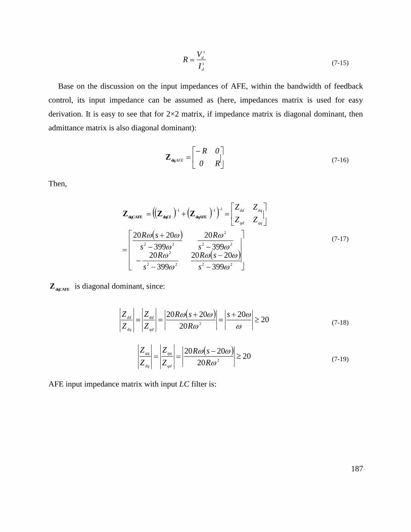
187
s
d
s
d
I
VR (7-15)
Base on the discussion on the input impedances of AFE, within the bandwidth of feedback
control, its input impedance can be assumed as (here, impedances matrix is used for easy
derivation. It is easy to see that for 2×2 matrix, if impedance matrix is diagonal dominant, then
admittance matrix is also diagonal dominant):
R0
0RAFEdq
Z (7-16)
Then,
2222
2
22
2
22
111
399
2020
399
20399
20
399
2020
s
sR
s
Rs
R
s
sR
ZZ
ZZ
qqqd
dqdd
dqAFEdqCfdqCAFEZZZ
(7-17)
dqCAFEZ is diagonal dominant, since:
2020
20
20202
s
R
sR
Z
Z
Z
Z
qd
dd
dq
dd (7-18)
2020
20202
R
sR
Z
Z
Z
Z
qd
dq
(7-19)
AFE input impedance matrix with input LC filter is:
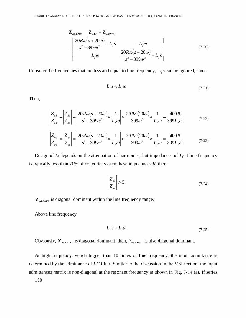
STABILITY ANALYSIS OF THREE-PHASE AC POWER SYSTEMS BASED ON MEASURED D-Q FRAME IMPEDANCES
188
sLs
sRL
LsLs
sR
ff
ff
22
22
399
2020399
2020
dqCAFEdqLfdqLCAFEZZZ
(7-20)
Consider the frequencies that are less and equal to line frequency, sLf
can be ignored, since
ff
LsL (7-21)
Then,
fffqd
dd
dq
dd
L
R
L
R
Ls
sR
Z
Z
Z
Z
399
4001
399
20201
399
2020222
(7-22)
fffdq
qd
L
R
L
R
Ls
sR
Z
Z
Z
Z
399
4001
399
20201
399
2020222
(7-23)
Design of Lf depends on the attenuation of harmonics, but impedances of Lf at line frequency
is typically less than 20% of converter system base impedances R, then:
5dq
dd
Z
Z (7-24)
dqLCAFEZ is diagonal dominant within the line frequency range.
Above line frequency,
ff
LsL (7-25)
Obviously, dqLCAFE
Z is diagonal dominant, then, dqLCAFE
Y is also diagonal dominant.
At high frequency, which bigger than 10 times of line frequency, the input admittance is
determined by the admittance of LC filter. Similar to the discussion in the VSI section, the input
admittances matrix is non-diagonal at the resonant frequency as shown in Fig. 7-14 (a). If series
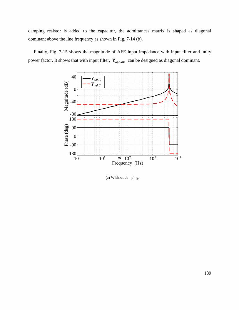
189
damping resistor is added to the capacitor, the admittances matrix is shaped as diagonal
dominant above the line frequency as shown in Fig. 7-14 (b).
Finally, Fig. 7-15 shows the magnitude of AFE input impedance with input filter and unity
power factor. It shows that with input filter, dqLCAFE
Y can be designed as diagonal dominant.
-80
-40
0
40
Mag
nit
ud
e (d
B)
-180
-90
0
90
180
Ph
ase
(deg
)
YddLC
YdqLC
Frequency (Hz)100 101 102 103 104ω
(a) Without damping.
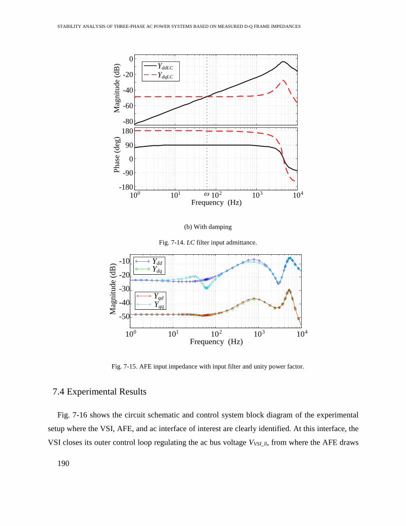
STABILITY ANALYSIS OF THREE-PHASE AC POWER SYSTEMS BASED ON MEASURED D-Q FRAME IMPEDANCES
190
-80
-60
-40
-20
0
Mag
nit
ude
(dB
)
-180
-90
0
90
180
Phas
e (d
eg)
YddLC
YdqLC
Frequency (Hz)100 101 102 103 104ω
(b) With damping
Fig. 7-14. LC filter input admittance.
Ydd
Ydq
Yqd
Yqq
Frequency (Hz)100 101 102 103 104
Mag
nit
ude
(dB
)
-50
-40
-30
-20
-10
Fig. 7-15. AFE input impedance with input filter and unity power factor.
7.4 Experimental Results
Fig. 7-16 shows the circuit schematic and control system block diagram of the experimental
setup where the VSI, AFE, and ac interface of interest are clearly identified. At this interface, the
VSI closes its outer control loop regulating the ac bus voltage VVSI_ll, from where the AFE draws
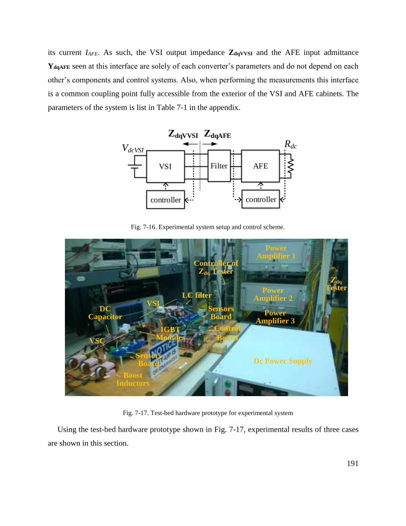
191
its current IAFE. As such, the VSI output impedance ZdqVVSI and the AFE input admittance
YdqAFE seen at this interface are solely of each converter’s parameters and do not depend on each
other’s components and control systems. Also, when performing the measurements this interface
is a common coupling point fully accessible from the exterior of the VSI and AFE cabinets. The
parameters of the system is list in Table 7-1 in the appendix.
VSI
controller
AFE
controller
Filter
ZdqVVSI ZdqAFE
VdcVSIRdc
Fig. 7-16. Experimental system setup and control scheme.
Dc Power Supply
VSI
VSC
Zdq
Tester
Power Amplifier 1
Power Amplifier 2
Power Amplifier 3
Controller of Zdq Tester
Control
Board
LC filter
Sensors Board
IGBT Modules
Sensors Board
Boost Inductors
DC Capacitor
Fig. 7-17. Test-bed hardware prototype for experimental system
Using the test-bed hardware prototype shown in Fig. 7-17, experimental results of three cases
are shown in this section.

STABILITY ANALYSIS OF THREE-PHASE AC POWER SYSTEMS BASED ON MEASURED D-Q FRAME IMPEDANCES
192
The first experiments is VSI feeding AFE working under unity power factor condition. Fig.
7-18 shows the time domain test results, which indicates the system is stable. Fig. 7-19 shows the
measured VSI output impedances, which shows the impedances matrix is diagonal. Fig. 7-20
shows the measured AFE input admittances, which shows the admittances matrix is diagonal.
Fig. 7-21 shows the eigenvalue loci of minor loop-gain of the VSI feeding AFE system over
plotted with d and q channel impedance ratios. Clearly, the first eigenvalue loci is equal to the d
channel impedance ratio between VSI and AFE, the second loci is equal to the q channel
impedance ratio between VSI and AFE.
Vdc_AFE
VVSI_abIAFE_b
IAFE_a
Fig. 7-18. Time domain test results of VSI feeding AFE with unity power factor.

193
-20
-10
0
10
20
30
-180
-90
0
90
180
Mag
nit
ud
e (d
B)
Ph
ase
(deg
)
Frequency (Hz)101 10 2 103 104
ZddVSI
ZqqVSI
ZdqVSI
ZqdVSI
Fig. 7-19. Meausred VSI output impedances.
-50
-30
-10
Mag
nit
ude
(dB
)
-540
-360
-180
0
180
Phas
e (d
eg)
Frequency (Hz)101 102 103 104
YddAFE
YdqAFE
YqdAFE
YqqAFE
Fig. 7-20. Measured AFE input admittances with unity power factor.

STABILITY ANALYSIS OF THREE-PHASE AC POWER SYSTEMS BASED ON MEASURED D-Q FRAME IMPEDANCES
194
1
2
ZddVSI∙YddAFE
ZqqVSI∙YqqAFE
-2 0 2 4 6
-4
-3
-2
-1
0
1
2
3
4
Real
Imagin
ary
Fig. 7-21. Eigenvalue loci over plotted with impedance ratios.
YddAFE
YdqAFE
YqdAFE
YqqAFE
Frequency (Hz)101 102 103 104
Mag
nit
ude
(dB
)P
has
e (d
eg)
-50
-30
-10
-900
-720
-540
-360
-180
0
180
Fig. 7-22. Measured YdqAFE with input filter.
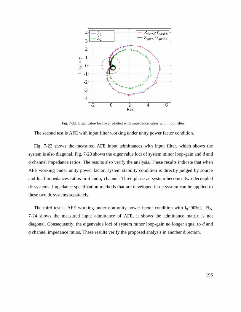
195
1
2
ZddVSI∙YddAFE
ZqqVSI∙YqqAFE
-2 0 2 4 6
-4
-3
-2
-1
0
1
2
3
4
Real
Imag
inar
y
Fig. 7-23. Eigenvalue loci over plotted with impedance ratios with input filter.
The second test is AFE with input filter working under unity power factor condition.
Fig. 7-22 shows the measured AFE input admittances with input filter, which shows the
system is also diagonal. Fig. 7-23 shows the eigenvalue loci of system minor loop-gain and d and
q channel impedance ratios. The results also verify the analysis. These results indicate that when
AFE working under unity power factor, system stability condition is directly judged by source
and load impedances ratios in d and q channel. Three-phase ac system becomes two decoupled
dc systems. Impedance specification methods that are developed in dc system can be applied to
these two dc systems separately.
The third test is AFE working under non-unity power factor condition with Iq=90%Id. Fig.
7-24 shows the measured input admittance of AFE, it shows the admittance matrix is not
diagonal. Consequently, the eigenvalue loci of system minor loop-gain no longer equal to d and
q channel impedance ratios. These results verify the proposed analysis in another direction.
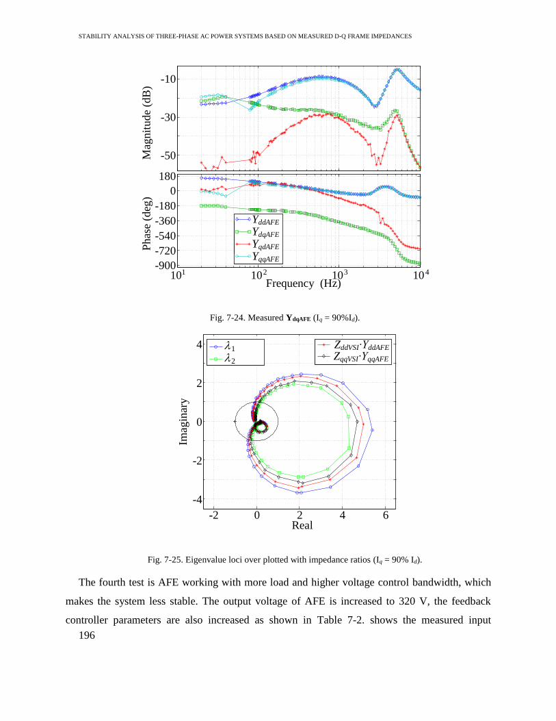
STABILITY ANALYSIS OF THREE-PHASE AC POWER SYSTEMS BASED ON MEASURED D-Q FRAME IMPEDANCES
196
Frequency (Hz)101 102 103 104
Mag
nit
ude
(dB
)P
has
e (d
eg)
-50
-30
-10
-900
-720
-540
-360
-180
0
180
YddAFE
YdqAFE
YqdAFE
YqqAFE
Fig. 7-24. Measured YdqAFE (Iq = 90%Id).
1
2
ZddVSI∙YddAFE
ZqqVSI∙YqqAFE
-2 0 2 4 6
-4
-2
0
2
4
Real
Imag
inar
y
Fig. 7-25. Eigenvalue loci over plotted with impedance ratios (Iq = 90% Id).
The fourth test is AFE working with more load and higher voltage control bandwidth, which
makes the system less stable. The output voltage of AFE is increased to 320 V, the feedback
controller parameters are also increased as shown in Table 7-2. shows the measured input
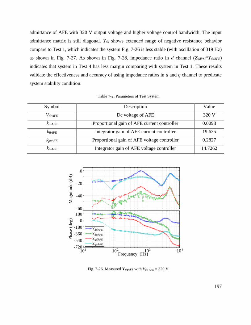
197
admittance of AFE with 320 V output voltage and higher voltage control bandwidth. The input
admittance matrix is still diagonal. Ydd shows extended range of negative resistance behavior
compare to Test 1, which indicates the system Fig. 7-26 is less stable (with oscillation of 319 Hz)
as shown in Fig. 7-27. As shown in Fig. 7-28, impedance ratio in d channel (ZddVSI*YddAFE)
indicates that system in Test 4 has less margin comparing with system in Test 1. These results
validate the effectiveness and accuracy of using impedance ratios in d and q channel to predicate
system stability condition.
Table 7-2. Parameters of Test System
Symbol Description Value
VdcAFE Dc voltage of AFE 320 V
kpiAFE Proportional gain of AFE current controller 0.0098
kiiAFE Integrator gain of AFE current controller 19.635
kpvAFE Proportional gain of AFE voltage controller 0.2827
kivAFE Integrator gain of AFE voltage controller 14.7262
Frequency (Hz)101 102 103 104
-60
-40
-20
0
-720
-540
-360
-180
0
180
Mag
nit
ude
(dB
)P
has
e (d
eg)
YddAFE
YdqAFE
YqdAFE
YqqAFE
Fig. 7-26. Measured YdqAFE with Vdc_AFE = 320 V.

STABILITY ANALYSIS OF THREE-PHASE AC POWER SYSTEMS BASED ON MEASURED D-Q FRAME IMPEDANCES
198
Vdc_AFE
VVSI_ab
IAFE_b
IAFE_a
319 Hz
Fig. 7-27. Time domain test results of the system with Vdc_AFE = 320 V.
-1
-0.5
0
0.5
1
-1.5 -1 -0.5 0 0.5
Real
Imag
inar
y
314 Hz
20 Hz
284 Hz
Test 1ZddVSI∙YddAFE
1
Test 4ZddVSI∙YddAFE
1
Fig. 7-28. Eigenvalue loci over plotted with impedance ratios for Test 1 and 4.

199
Chapter 8 Conclusions and Future Work
The impedance-based stability analysis has now been used for over 20 years in dc systems,
having become an essential component of their design and integration. In effect, by using this
method, system integrators can easily specify valid ranges for the impedance of components in
order to ensure the system stability when using equipment from different suppliers. For ac
systems however, this method is still not common practice. Accordingly, this research has strived
to demonstrate the experimental accuracy of stability prediction in both frequency domain and
time domain that can be attained in ac systems when using this approach. This has the potential
to enable the use of impedance specification as a design tool for future ac systems. To this end,
an experimental setup comprised of a voltage source inverter acting as ac source, and a three-
phase boost rectifier acting as constant power load, was built. Three experiments were then
conducted and analyzed, showing stable, critical stable, and unstable conditions by adjusting the
control bandwidth of the source converter—modifying its output impedance. The corresponding
ac impedances in the d-q frame of both source and load subsystems were then measured, and the
Generalized Nyquist stability Criterion (GNC) was applied, showing how both stable and
unstable conditions could be effectively predicted and verified using this approach. Time domain
and frequency domain waveforms and plots were used to illustrate this.
This research also presents an analysis of grid-tied inverter small-signal impedance in d-q
frame under different control strategies. Influences of PLL, current and power feedback control
to the inverter impedance are discussed. Some important features of inverter impedance are
discussed. These features indicates that grid-tied inverter working as current source could
destabilize the system due to the negative incremental resistor of Zqq. This negative incremental
resistor behavior is a results of PLL. Increasing of PLL bandwidth extends the frequency range
of this behavior. Increasing of inverter power level decreases the absolute value of the resistor. A
brief simulation example shows that under weak grid condition, a small increase of the PLL
bandwidth could lead the system to unstable condition. The example also shows how the
proposed model can be used to predict such instability. Hardware measurements verify the
proposed model. The model gives insight of the grid-tied inverter behavior in the grid. Harmonic

STABILITY ANALYSIS OF THREE-PHASE AC POWER SYSTEMS BASED ON MEASURED D-Q FRAME IMPEDANCES
200
resonance and instability issues reported in the literature can be analyzed using the characterized
impedance model.
Then this research proposes an impedance-based analysis method to analyze the grid-
synchronization stability issue in paralleled three-phase converter systems including grid-tied
inverter, active front end rectifier, local passive load, and grid impedance. The proposed method
shows that the multi-variable GNC and GINC can be used to predict the system stability based
on the grid and inverter impedances in the synchronous d-q frame. Furthermore, the instability is
found to be caused by q channel impedance interaction. Experimental results verify the analysis
and the proposed method.
Impedance-based analysis for active frequency drift islanding detection methods is also
discussed in this disseration. To do the analysis, the output impedance of a grid-tied inverter was
modeled with PLL-based AFD method. The Zqq of the grid-tied inverter output impedance
features a negative incremental impedance. Since a grid-tied inverter q channel impedance
magnitude is equal to the dc impedance magnitude of the local load, impedance interaction
happens when islanding event happens. With big feed forward gain N for islanding detection, the
phase of Zqq is shown to drop below –180°. Under islanding condition, the inverter system
became unstable with a frequency drift away from steady-state. Based on the impedance of the
inverter, it could be concluded that the grid-tied inverter with AFD islanding method has the
potential to destabilize the grid-connected inverter system when the grid is weak. Experimental
results verified the analysis.
Finally, an attempt to do load impedance specification for three-phase ac system is
presentated. The research first reviewed impedance-based small-signal stability analysis of dc
distributed power system. It is well known that stability margin and forbidden region can be
defined for dc system to ensure small-signal stability. Load impedance specification can also be
defined which greatly helps the system integration for dc system. Small-signal stability of
balanced three-phase ac system can be predicted using source and load impedance in d-q frame,
similar stability margin and load impedance specification cannot be done because of the MIMO
system coupling in three-phase ac system. This research found that when three-phase ac system

201
working under high power factor condition, which is the case for power electronics interfaced
distributed power system for micro-grid, more electric aircraft and ship, system could be
decoupled in d-q frame. Then ac system becomes two independent dc systems. Load impedance
specification can be done separately for d and q channel as two dc systems. Limitation of the
proposed method is system should working under nearly unity power factor condition.
Simulation and measurement are used to verify the analysis.
STABILITY ANALYSIS OF THREE-PHASE AC POWER SYSTEMS BASED ON MEASURED D-Q FRAME IMPEDANCES
202
REFERENCES
[1] R. E. Thomas, “The stability of aircraft D-C power systems with inverter loads,” AIEE
Trans. Applicat. Ind., vol. 76, pp. 183-188, Sep. 1957.
[2] Z. Yao, P. G. Therond, and B. Davat, “Stability analysis of power systems by the generalised
Nyquist criterion,” in Proc. Int. Conf. on control, Mar. 1994, pp. 739–744.
[3] M. Belkhayat, “Stability criteria for ac power systems with regulated loads,” Ph.D.
dissertation, Purdue Univ., West Lafayette, IN, Dec. 1997.
[4] A. G. J. MacFarlane and I. Postlethwaite, “The generalized Nyquist stability criterion and
multivariable root loci,” Int. J. of Control, vol. 25, no. 1, pp. 81–127, 1977.
[5] N. Sokal, “System oscillations from negative input resistance at power input port of
switching-mode regulator, amplifier, dc/dc converter, or dc/ac inverter,” in Proc. IEEE
Power Electron. Spec. Conf., Sep. 1973, pp. 138–140.
[6] B. H. Cho and F. C. Y. Lee, “Modeling and analysis of spacecraft power systems,” IEEE
Trans. Power Electron., vol. 3, no. 1, pp. 44-54, Jan. 1988.
[7] I. Lazbin and B. R. Needham, “Analysis of the stability margins of the Space Station
Freedom Electrical Power System,” in Proc. IEEE Power Electron. Spec. Conf., Jun. 1993,
pp. 839–845.
[8] K. J. Karimi, A. J. Booker, A. C. Mong, and B. Manners, “Verification of Space Station
secondary power system stability using design of experiment,” in Proc. Energy Convers.
Eng. Conf., Jul. 1997, pp. 526–531.

203
[9] T. C. Wang and J. B. Raley, “Electrical power system stability assurance for the International
Space Station,” in Proc. Energy Convers. Eng. Conf., Jul. 1997, pp. 246–252.
[10] H. W. Wallen and S. J. Fu, “United States laboratory element electrical power system
verification approach,” J. Propulsion and Power, vol. 13, no. 4, Jul. 1997.
[11] A. Griffo and J. Wang, “Stability analysis of “more electric” aircraft hybrid electrical
power systems,” in Proc. Int. Conf. Elect. Mach. Syst., Aug. 2011, pp. 1–8.
[12] K. N. Areerak, S. V. Bozhko, G. M. Asher, L. De Lillo, and D. W. P. Thomas, “Stability
Study for a Hybrid AC-DC More-Electric Aircraft Power System,” IEEE Trans. Aerosp.
Electron. Syst., vol. 48, no. 1, pp. 329–347, Jan. 2012.
[13] H. Zhang, C. Saudemont, B. Robyns, N. Huttin, and R. Meuret, "Stability analysis on the
DC Power Distribution System of More Electric Aircraft," in Proc. Power Electron. Motion
Control Conf., Sep. 2008, pp. 1523–1528.
[14] F. Gao, S. Bozhko, S. Yeoh, G. Asher, and P. Wheeler, “Stability of multi-source droop-
controlled Electrical Power System for more-electric aircraft,” in Proc. IEEE Int. Conf.
Intell. Engery Power Syst., Jun. 2014, pp. 122–126.
[15] A. Emadi, A. Khaligh, C. H. Rivetta, and G. A. Williamson, “Constant power loads and
negative impedance instability in automotive systems: definition, modeling, stability, and
control of power electronic converters and motor drives,” IEEE Trans. Veh. Technol., vol.
55, no. 4, pp. 1112–1125, Jul. 2006.
[16] S. D. Sudhoff, K. A. Corzine, S. F. Glover, H. J. Hegner, and H. N. Robey, Jr., “DC link
stabilized field oriented control of electric propulsion systems,” IEEE Trans. Engery
Convers., vol. 13, no.1, pp. 27–33, Mar. 1998.

STABILITY ANALYSIS OF THREE-PHASE AC POWER SYSTEMS BASED ON MEASURED D-Q FRAME IMPEDANCES
204
[17] J. G. Ciezki and R. W. Ashton, “Selection and stability issues associated with a navy
shipboard DC zonal electric distribution system,” IEEE Trans. Power Del., vol. 15, no. 2, pp.
665–669, Apr. 2000.
[18] G. Sulligoi, D. Bosich, G. Giadrossi, Z. Lin, M. Cupelli, and A. Monti, “Multiconverter
medium voltage dc power systems on ships: constant-power loads instability solution using
linearization via state feedback control,” IEEE Trans. Smart Grid, vol. 5, no. 5 pp. 2543–
2552, Sep. 2014.
[19] D. P. Ariyasinghe and D. M. Vilathgamuwa, “Stability analysis of microgrids with
constant power loads,” in Proc. Int. Conf. Sustainable Energy Technol., Nov. 2008, pp. 279–
284.
[20] A. Kwasinski and C. N. Onwuchekwa, “Dynamic Behavior and Stabilization of DC
Microgrids With Instantaneous Constant-Power Loads,” IEEE Trans. Power Electron., vol.
26, no. 3, pp. 822–834, Mar. 2011.
[21] A. A. A. Radwan and Y. A. R. I. Mohamed, “Linear Active Stabilization of Converter-
Dominated DC Microgrids,” IEEE Trans. Smart Grid, vol. 3, no. 1, pp. 203–216, Mar. 2012.
[22] A. A. A. Radwan and Y. A. R. I. Mohamed, “Modeling, Analysis, and Stabilization of
Converter-Fed AC Microgrids With High Penetration of Converter-Interfaced Loads,” IEEE
Trans. Smart Grid, vol. 3, no. 3, pp. 1213–1225, Sep. 2012.
[23] S. Anand and B. G. Fernandes, “Reduced-Order Model and Stability Analysis of Low-
Voltage DC Microgrid,” IEEE Trans. Ind. Electron., vol. 60, no. 11, pp. 5040–5049, Nov.
2013.
205
[24] V. Pala, P. Han, P. Wright, M. M. Hella, and T. P. Chow, “Integrated high-frequency
power converters based on GaAs pHEMT: technology characterization and design
examples,” IEEE Trans. Power Electron., vol. 27, no. 5, pp. 2644–2656, May 2012.
[25] J. W. Kolar, F. Krismer, Y. Lobsiger, J. Muhlethaler, T. Nussbaumer, and J. Minibock,
“Extreme efficiency power electronics,” in Proc. Int. Conf. Integr. Power Electron. Syst.,
Mar. 2012, pp. 1-22.
[26] K. Norling, C. Lindholm, and D. Draxelmayr, “An optimized driver for SiC JFET-based
switches enabling converter operation with more than 99% efficiency,” IEEE J. Solid-State
Circuits, vol. 47, no. 12, pp. 3095–3104, Dec. 2012.
[27] Y. F. Wu, J. Gritters, L. Shen, R. P. Smith, and B. Swenson, “kV-class GaN-on-Si
HEMTs enabling 99% efficiency converter at 800 V and 100 kHz,” IEEE Trans. Power
Electron., vol. 29, no. 6, pp. 2634–2637, Jun. 2014.
[28] R. D. Middlebrook, “Input filter considerations in design and application of switching
regulators,” in Proc. IEEE Ind. Applicat. Soc. Conf., Oct. 1976, pp. 94–107.
[29] K. N. Areerak, S. V. Bozhko, G. M. Asher, L. D. Lillo, and D. W. P. Thomas, “Stability
study for a hybrid ac-dc more-electric aircraft power system,” IEEE Trans. Aerosp. Electron.
Syst., vol. 48, no. 1, pp. 329–347, Jan. 2012.
[30] N. Bottrell, M. Prodanovic, and T. C. Green, “Dynamic stability of a microgrid with an
active load,” IEEE Trans. Power Electron., vol. 28, no. 11, pp. 5107–5119, Nov. 2013.
[31] R. D. Middlebrook, “Measurement of loop gain in feedback systems,” Int. J. Electron.,
vol. 38. no. 4, pp. 485–512, 1975.

STABILITY ANALYSIS OF THREE-PHASE AC POWER SYSTEMS BASED ON MEASURED D-Q FRAME IMPEDANCES
206
[32] Y. Panov and M. M. Jovanovic, “Stability and dynamic performance of current-sharing
control for paralleled voltage regulator modules,” IEEE Trans. Power Electron., vol. 17, no.
2, pp. 172-179, Mar. 2002.
[33] J. Morroni, R. Zane, and D. Maksimovic, “An online stability margin monitor for
digitally controlled switched-mode power supplies,” IEEE Trans. Power Electron., vol. 24,
no. 11, pp. 2639-2648, Nov. 2009.
[34] J. Castello and J. M. Espi, “DSP implementation for measuring the loop gain frequency
response of digitally controlled power converters,” IEEE Trans. Power Electron., vol. 27, no.
9, pp. 4113-4121, Sep. 2012.
[35] C. M. Wildrick, F. C. Lee, B. H. Cho, and B. Choi, “A method of defining the load
impedance specification for a stable distributed power system,” IEEE Trans. Power
Electron., vol. 10, no. 3, pp. 280–285, May 1995.
[36] S. D. Sudhoff, S. F. Glover, P. T. Lamm, D. H. Schmucker, and D. E. Delisle,
“Admittance space stability analysis of power electronic systems,” IEEE Trans. Aerosp.
Electron. Syst., vol. 36, no. 3, pp. 965–973, Jul. 2000.
[37] X. Feng, J. Liu, and F. C. Lee, “Impedance specification for stable dc distributed power
systems,” IEEE Trans. Power Electron., vol. 17, no. 2, pp. 157–162, Mar. 2002.
[38] S. Vesti, T. Suntio, J. A. Oliver, R. Prieto, and J. A. Cobos, “Impedance-based stability
and transient-performance assessment applying maximum peak criteria,” IEEE Trans. Power
Electron., vol. 28, no. 5, pp. 2099–2104, May 2013.
207
[39] H. Mao, D. Boroyevich, and F. C. Lee, “Novel reduced-order small-signal model of a
three-phase PWM rectifier and its application in control design and system analysis,” IEEE
Trans. Power Electron., vol. 13, no. 3, pp. 511–521, May 1998.
[40] B. H. Cho and B. Choi, “Analysis and design of multi-stage distributed power systems,”
in Proc. INTELEC Conf., Nov. 1991, pp. 220–226.
[41] S. Hiti, V. Vlatkovic, D. Borojevic, and F. C. Lee, “A new control algorithm for three-
phase PWM buck rectifier with input displacement factor compensation,” IEEE Trans.
Power Electron., vol. 9, no. 2, pp. 173–180, Mar. 1994.
[42] A. G. J. MacFarlane and I. Postlethwaite, “The generalized Nyquist stability criterion and
multivariable root loci,” Int. J. of Control, vol. 25, no. 1, pp. 81–127, 1977.
[43] I. Postlethwaite, “A generalizd inverse Nyquist stability criterion,” Int. J. of Control, vol.
26, pp. 325–340, 1977.
[44] H. Jing, K. A. Corzine, and M. Belkhayat, “Small-signal impedance measurement of
power-electronics-based ac power systems using line-to-line current injection,” IEEE Trans.
Power Electron., vol. 24, no. 2, pp. 445–455, Feb. 2009.
[45] Y. A. Familiant, H. Jing, K. A. Corzine, and M. Belkhayat, “New techniques for
measuring impedance characteristics of three-phase ac power systems,” IEEE Trans. Power
Electron., vol. 24, no. 7, pp. 1802–1810, Jul. 2009.
[46] G. Francis, R. Burgos, D. Boroyevich, F. Wang, and K. Karimi, “An algorithm and
implementation system for measuring impedance in the d-q domain,” in Proc. Energy
Convers. Congr. Expo., Sep. 2011, pp. 3221–3228.
STABILITY ANALYSIS OF THREE-PHASE AC POWER SYSTEMS BASED ON MEASURED D-Q FRAME IMPEDANCES
208
[47] Z. Shen, M. Jaksic, P. Mattavelli, D. Boroyevich, J. Verhulst, and M. Belkhayat, “Design
and implementation of three-phase ac impedance measurement unit (IMU) with series and
shunt injection,” in Proc. 28th Annu. Appl. Power Electron. Conf. Expo., Mar. 2013, pp.
2674–2681.
[48] V. Valdivia, A. Lazaro, A. Barrado, P. Zumel, C. Fernandez, and M. Sanz, “Impedance
identification procedure of three-phase balanced voltage source inverters based on transient
response measurements,” IEEE Trans. Power Electron., vol. 26, no. 12, pp. 3810–3816, Dec.
2011.
[49] I. Cvetkovic, M. Jaksic, D. Boroyevich, P. Mattavelli, F. C. Lee, S. Zhiyu, S. Ahmed, and
D. Dong, “Un-terminated, low-frequency terminal-behavioral d-q model of three-phase
converters,” in Proc. Energy Convers. Congr. Expo., Sep. 2011, pp. 791–798.
[50] P. Kundur, Power system stability and control. New York: McGraw-Hill, 1994.
[51] P. Brogan and R. Yacamini, “Harmonic control using an active drive,” in Proc. IEE
Electr. Power Appl., Jan. 2003, pp. 14-20.
[52] S. Bernet, S. Ponnaluri, and R. Teichmann, “Design and loss comparison of matrix
converters, and voltage-source converters for modern AC drives,” IEEE Trans. Ind.
Electron., vol. 49, no. 2, pp. 304-314, Apr. 2002.
[53] D. G. Holmes and T. Lipo, Pulse Width Modulation for Power Converters: Principles
and Practice. Piscataway, NJ: IEEE Press, 2003.
[54] S. Hiti, D. Boroyevich, and C. Cuadros, “Small-signal modeling and control of three-
phase PWM converters,” in Proc. IEEE Ind. Applicat. Soc. Annu.. Meeting, Oct. 1994, pp.
94–107.

209
[55] S. Hiti, and D. Boroyevich, “Small-signal modeling of three-phase PWM modulators,”
in Proc. IEEE Power Electron. Spec. Conf., Jun. 1996, pp. 550–555.
[56] S. Buso and P. Mattavelli, “Digital Control in Power Electronics,” Synthesis Lectures on
Power Electronics, vol. 1, no. 1, pp. 1–158, Jan. 2006.
[57] Z. Zhang and L. Xu, “Dead-Time Compensation of Inverters Considering Snubber and
Parasitic Capacitance,” IEEE Trans. Power Electron., vol. 29, pp. 3179-3187, Jun. 2014.
[58] F. Chierchie, L. Stefanazzi, E. E. Paolini, and A. R. Oliva, “Frequency Analysis of PWM
Inverters With Dead-Time for Arbitrary Modulating Signals,” IEEE Trans. Power Electron.,
vol. 29, pp. 2850-2860, Jun. 2014.
[59] F. Gonzalez-Espin, E. Figueres, G. Garcera, R. Gonzalez-Medina, and M. Pascual,
“Measurement of the loop gain frequency response of digitally controlled power converters,”
IEEE Trans. Ind. Electron., vol. 53, no. 5, vol. 57, pp. 2785-2796, Aug. 2010.
[60] B. Bahrani, A. Karimi, B. Rey, and A. Rufer, “Decoupled dq-Current Control of Grid-
Tied Voltage Source Converters Using Nonparametric Models,” IEEE Trans. Ind. Electron.,
vol. 60, pp. 1356-1366, Apr. 2013.
[61] B. Bahrani, M. Vasiladiotis, and A. Rufer, “High-Order Vector Control of Grid-
Connected Voltage-Source Converters With LCL-Filters,” IEEE Trans. Ind. Electron., vol.
61, pp. 2767-2775, Jun. 2014.
[62] F. Blaabjerg, Z. Chen, and S. B. Kjaer, “Power electronics as efficient interface in
dispersed power generation systems,” IEEE Trans. Power Electron., vol. 19, no. 5, pp. 1184–
1194, Sep. 2004.

STABILITY ANALYSIS OF THREE-PHASE AC POWER SYSTEMS BASED ON MEASURED D-Q FRAME IMPEDANCES
210
[63] C. Se-Kyo, “A phase tracking system for three phase utility interface inverters,” IEEE
Trans. Power Electron., vol. 15, no. 3, pp. 431–438, May 2000.
[64] F. Blaabjerg, R. Teodorescu, M. Liserre, and A. V. Timbus, “Overview of control and
grid synchronization for distributed power generation systems,” IEEE Trans. Ind. Electron.,
vol. 53, no. 5, pp. 1398–1409, Oct. 2006.
[65] D. Jovcic, L. A. Lamont, and L. Xu, “VSC transmission model for analytical studies,” in
Proc. IEEE Power Eng. Soc. Gen. Meeting, Jul. 2003, pp. 1737–1742
[66] L. Harnefors, M. Bongiorno, and S. Lundberg, “Input-admittance calculation and shaping
for controlled voltage-source converters,” IEEE Trans. Ind. Electron., vol. 54, no. 6, pp.
3323–3334, Dec. 2007.
[67] M. Cespedes and S. Jian, “Impedance shaping of three-phase grid-parallel voltage-source
converters,” in Proc. 27th Annu. Appl. Power Electron. Conf. Expo., Mar. 2012, pp. 754–
760.
[68] D. Dong, B. Wen, P. Mattavelli, D. Boroyevich, and Y. Xue, “Grid-synchronization
modeling and its stability analysis for multi-paralleled three-phase inverter systems,” in Proc.
28th Annu. Appl. Power Electron. Conf. Expo., Mar. 2013, pp. 439-446.
[69] M. Schweizer and J. W. Kolar, “Shifting input filter resonances - an intelligent converter
behavior for maintaining system stability,” in Proc. Int. Power Electron. Conf. ECCE Asia,
May 2010, pp. 906–913.
[70] S. Bernet, “Recent developments of high power converters for industry and traction
applications,” IEEE Trans. Power Electron., vol. 15, no. 6, pp. 1102–1117, Nov. 2000.

211
[71] J. Sun, “Small-signal methods for ac distributed power systems—A Rewiew,” IEEE
Trans. Power Electron., vol. 24, no. 11, pp. 2545–2554, Nov. 2009.
[72] R. Burgos, D. Boroyevich, F. Wang, K. Karimi, and G. Francis, “On the ac stability of
high power factor three-phase rectifiers, ” in Proc. Energy Convers. Congr. Expo., Sep.
2010, pp. 2047–2054.
[73] D. G. Holmes and T. Lipo, Pulse Width Modulation for Power Converters: Principles
and Practice. Piscataway, NJ: IEEE Press, 2003.
[74] J. Rocabert, A. Luna, F. Blaabjerg, and P. Rodriguez, “Control of Power Converters in
AC Microgrids,” IEEE Trans. Power Electron., vol. 27, pp. 4734–4749, Nov. 2012.
[75] J. H. R. Enslin and P. J. M. Heskes, “Harmonic interaction between a large number of
distributed power inverters and the distribution network,” IEEE Trans. Power Electron., vol.
19, pp. 1586–1593, Nov. 2004.
[76] M. Liserre, R. Teodorescu, and F. Blaabjerg, “Stability of photovoltaic and wind turbine
grid-connected inverters for a large set of grid impedance values,” IEEE Trans. Power
Electron., vol. 21, pp. 263–272, Jan. 2006.
[77] M. Cespedes and J. Sun, “Renewable Energy Systems Instability Involving Grid-Parallel
Inverters,” in Proc. 24th Annu. Appl. Power Electron. Conf. Expo., Mar. 2009, pp. 1971–
1977.
[78] E. Vittal, M. O'Malley, and A. Keane, “A Steady-State Voltage Stability Analysis of
Power Systems With High Penetrations of Wind,” IEEE Trans. Power Syst., vol. 25, pp.
433–442, Feb. 2010.

STABILITY ANALYSIS OF THREE-PHASE AC POWER SYSTEMS BASED ON MEASURED D-Q FRAME IMPEDANCES
212
[79] J. Sun, “Impedance-Based Stability Criterion for Grid-Connected Inverters,” IEEE Trans.
Power Electron., vol. 26, pp. 3075–3078, Nov. 2011.
[80] M. Cespedes and J. Sun, “Impedance shaping of three-phase grid-parallel voltage-source
converters,” in Proc. 27th Annu. Appl. Power Electron. Conf. Expo., Mar. 2012, pp. 754–
760.
[81] B. Wen, D. Boroyevich, R. Burgos, P. Mattavelli, and Z. Shen, “Influence of phase-
locked loop on dq frame impdance of three-phase voltage-source converters and the impact
on system stability,” in Proc. 2013 CPES Power Electron. Conf., Apr. 6–8, 2013.
[82] M. Cespedes and J. Sun, “Impedance modeling and analysis of grid-connected voltage-
source converters,” IEEE Trans. Power Electron., vol. 29, pp. 1254–1261, Mar. 2014.
[83] K. M. Alawasa, Y. A. R. I. Mohamed, and W. Xu, “Modeling, Analysis, and Suppression
of the Impact of Full-Scale Wind-Power Converters on Subsynchronous Damping,” IEEE
Syst. J., vol. 7, pp. 700–712, Dec. 2013.
[84] K. M. Alawasa, Y. A. R. I. Mohamed, and W. Xu, “Active Mitigation of Subsynchronous
Interactions Between PWM Voltage-Source Converters and Power Networks,” IEEE Trans.
Power Electron., vol. 29, pp. 121–134, Jan. 2014.
[85] T. Messo, J. Jokipii, A. Makinen, and T. Suntio, “Modeling the grid synchronization
induced negative-resistor-like behavior in the output impedance of a three-phase photovoltaic
inverter,” in Proc. 4th IEEE Int. Symp. Power Electron. Distrib. Generation, Jul. 2013, pp.
1–7.

213
[86] L. Zhang, L. Harnefors, and H. P. Nee, “Power-Synchronization Control of Grid-
Connected Voltage-Source Converters,” IEEE Trans.Power Syst., vol. 25, pp. 809-820, May
2010.
[87] Q. C. Zhong, P. L. Nguyen, Z. Ma, and W. Sheng, “Self-Synchronized Synchronverters:
Inverters Without a Dedicated Synchronization Unit,” IEEE Trans. Power Electron., vol. 29,
pp. 617-630, Feb. 2014.
[88] P. Mattavelli, F. Polo, F. Dal Lago, and S. Saggini, “Analysis of Control-Delay
Reduction for the Improvement of UPS Voltage-Loop Bandwidth,” IEEE Trans. Ind.
Electron., vol. 55, pp. 2903-2911, Aug. 2008.
[89] P. Rodriguez, J. Pou, J. Bergas, J. I. Candela, R. P. Burgos, and D. Boroyevich,
“Decoupled Double Synchronous Reference Frame PLL for Power Converters Control,”
IEEE Trans. Power Electron., vol. 22, pp. 584–592, Mar. 2007.
[90] R. Teodorescu, M. Liserre, and P. Rodriguez, Grid Converters for Photovoltaic and Wind
Power Systems. Piscataway, NJ: Wiley-IEEE Press 2011.
[91] D. N. Zmood, D. G. Holmes, and G. H. Bode, “Frequency-domain analysis of three-
phase linear current regulators,” IEEE Trans. Ind. Appl., vol. 37, no. 2, pp. 601–610, Apr.
2001.
[92] B. Wen, D. Boroyevich, R. Burgos, and P. Mattavelli, “Input impedance of voltage
source converter with stationary frame linear current regulators and phase-locked loop,” in
Proc. Energy Convers. Congr. Expo., Sept. 2013, pp. 4207–4213.

STABILITY ANALYSIS OF THREE-PHASE AC POWER SYSTEMS BASED ON MEASURED D-Q FRAME IMPEDANCES
214
[93] X. Wang, F. Blaabjerg, and W. Wu, “Modeling and analysis of harmonic stability in an
ac power-electronics-based power system,” IEEE Trans. Power Electron., vol. 29, no. 12, pp.
6421-6432, Dec. 2014.
[94] S. Golestan, M. Monfared, and F. D. Freijedo, “Design-oriented study of advanced
synchronous reference frame phase-locked loops,” IEEE Trans. Power Electron., vol. 28, no.
2, pp. 765-778, Feb. 2013.
[95] S. Skogestad and I. Postlethwaite, Multivariable feedback control : analysis and design.
Hoboken, NJ: John Wiley, 2005.
[96] “IEEE Standard for Interconnecting Distributed Resources With Electric Power
Systems,” IEEE Std 1547-2003, pp. 0_1-16, 2003.
[97] M. E. Ropp, M. Begovic, and A. Rohatgi, “Analysis and performance assessment of the
active frequency drift method of islanding prevention,” Energy Conversion, IEEE
Transactions on, vol. 14, pp. 810-816, 1999.
[98] L. A. C. Lopes and S. Huili, “Performance assessment of active frequency drifting
islanding detection methods,” Energy Conversion, IEEE Transactions on, vol. 21, pp. 171-
180, 2006.
[99] D. Velasco, C. Trujillo, G. Garcera, and E. Figueres, “An Active Anti-Islanding Method
Based on Phase-PLL Perturbation,” Power Electronics, IEEE Transactions on, vol. 26, pp.
1056-1066, 2011.
[100] A. Yafaoui, W. Bin, and S. Kouro, “Improved Active Frequency Drift Anti-islanding
Detection Method for Grid Connected Photovoltaic Systems,” Power Electronics, IEEE
Transactions on, vol. 27, pp. 2367-2375, 2012.

215
[101] D. Pengwei, Y. Zhihong, E. E. Aponte, J. K. Nelson, and F. Lingling, “Positive-
Feedback-Based Active Anti-Islanding Schemes for Inverter-Based Distributed Generators:
Basic Principle, Design Guideline and Performance Analysis,” Power Electronics, IEEE
Transactions on, vol. 25, pp. 2941-2948, 2010.
[102] D. Dong, D. Boroyevich, P. Mattavelli, B. Wen, and X. Yaosuo, “Anti-islanding
protection in three-phase converters using grid synchronization small-signal stability,” in
Energy Conversion Congress and Exposition (ECCE), 2012 IEEE, 2012, pp. 2712-2718.
[103] W. Xiaoyu, W. Freitas, and X. Wilsun, “Dynamic Non-Detection Zones of Positive
Feedback Anti-Islanding Methods for Inverter-Based Distributed Generators,” Power
Delivery, IEEE Transactions on, vol. 26, pp. 1145-1155, 2011.
[104] H. H. Zeineldin and M. M. A. Salama, “Impact of Load Frequency Dependence on the
NDZ and Performance of the SFS Islanding Detection Method,” Industrial Electronics, IEEE
Transactions on, vol. 58, pp. 139-146, 2011.
[105] C. D. Xu and K. W. E. Cheng, “A survey of distributed power system-AC versus DC
distributed power system,” in Proc. Int. Conf. on Power Electron. Syst. and Appl., Jun. 2011,
pp. 1–12.
[106] D. Boroyevich, R. Burgos, L. Arnedo, and F. Wang, “Synthesis and integration of future
electronic power distribution systems,” in Proc. Power Conv. Conf., Nagoya, Japan, Apr.
2007, pp. 1–8.
[107] M. Tabari and A. Yazdani, “Stability of a DC distribution system for power system
integration of plug-in hybrid electric vehicles,” IEEE Trans. Smart Grid, 2014.
STABILITY ANALYSIS OF THREE-PHASE AC POWER SYSTEMS BASED ON MEASURED D-Q FRAME IMPEDANCES
216
[108] F. Briz, M. W. Degner, and R. D. Lorenz, “Analysis and design of current regulators
using complex vectors,” IEEE Trans. Industry Applicat., vol. 36, pp. 817–825, May/Jun.
2000.
[109] N. Hensgens, M. Silva, J. A. Oliver, J. A. Cobos, S. Skibin, and A. Ecklebe, “Optimal
design of ac EMI filters with damping networks and effect on the system power factor,” in
Proc. Energy Convers. Congr. Expo., Sep. 2012, pp. 637–644.
[110] K. Hatua, A. K. Jain, D. Banerjee, and V. T. Ranganathan, “Active damping of output LC
filter resonance for vector-controlled VSI-fed ac motor drives,” IEEE Trans. Ind. Electron.,
vol. 59, pp. 334–342, Jan. 2012.
[111] D. Ke, L. Ping, K. Yong, and C. Jian, “Decoupling current control for voltage source
converter in synchronous roating frame,” in Proc. 4th IEEE Intern. Conf. Power Electron.
Drive Syst., Oct. 2001, pp. 39–43.
[112] B. Bahrani, S. Kenzelmann, and A. Rufer, “Multivariable-PI-based d-q current control of
voltage source converters with superior axis decoupling capability,” IEEE Trans. Ind.
Electron., vol. 58, no. 7, pp. 3016–3026, Jul. 2011.
[113] B. Wen, D. Boroyevich, P. Mattavelli, S. Zhiyu, and R. Burgos, “Experimental
verification of the generalized Nyquist stability criterion for balanced three-phase ac systems
in the presence of constant power loads,” in Proc. Energy Convers. Congr. Expo., Sep. 2012,
pp. 3926–3933.