chapter 1. basic electron optics lecture 4 -...
TRANSCRIPT

CHEM 793, 2011 Fall
Chapter 1. Basic Electron OpticsLecture 4
• Electron Scattering (cont’)• Instrumentation
CHEM 793, 2011 Fall
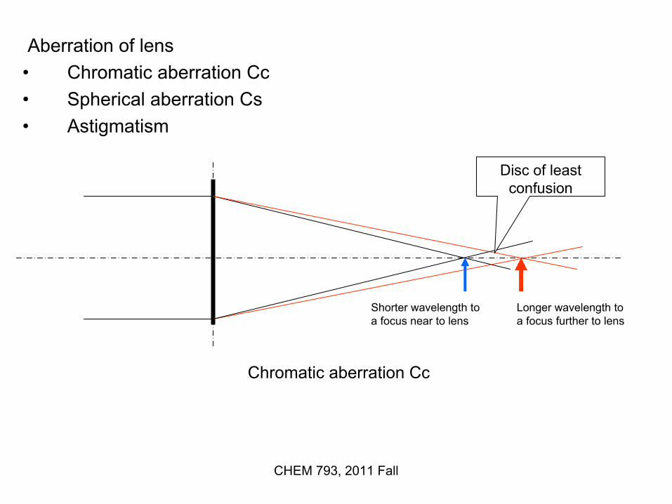
Aberration of lens• Chromatic aberration Cc• Spherical aberration Cs• Astigmatism
Disc of least confusion
Shorter wavelength to a focus near to lens
Longer wavelength to a focus further to lens
Chromatic aberration Cc

CHEM 793, 2011 Fall
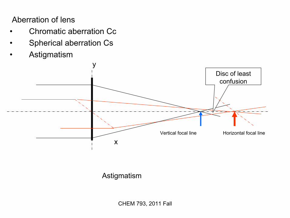
Aberration of lens• Chromatic aberration Cc• Spherical aberration Cs• Astigmatism
Disc of least confusion
Focus for marginal rays is nearer to lens than the focus for paraxial rays
Axial focus
Spherical aberration Cc
CHEM 793, 2011 Fall
Aberration of lens• Chromatic aberration Cc• Spherical aberration Cs• Astigmatism
Disc of least confusion
Vertical focal line Horizontal focal line
Astigmatism
y
x

CHEM 793, 2011 Fall
Price of the FEI Titan 300 kV TEM with Cs corrector (2006 release) is $3.5 M.
CHEM 793, 2011 Fall
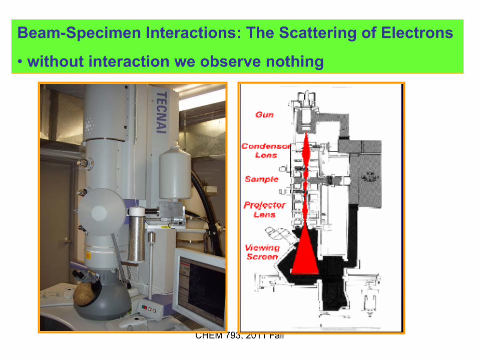
Beam-Specimen Interactions: The Scattering of Electrons
• without interaction we observe nothing

CHEM 793, 2011 Fall
Electron Microscopy
Specimen
Scanning Electron Microscope (SEM) Dealing mainly with Surface
Electron Beam
Backscattered Secondary Electron to Image Specimen Topography
Transmission Electron Microscope (TEM) Dealing mainly with Internal Structure
Transmitted and Diffracted Electron to Image Specimen Internal Structure
CHEM 793, 2011 Fall
Scattering Events
Single Scattering: each electron scatters only once on average while traversing the sample
• good for TEM analytical work
Plural Scattering: each electron scatters more than once but less than 20 times
Multiple Scattering: each electron scatters more than 20 times as it traverses the sample
• sample is too thick for any reasonable analytical work, difficult to predict what will happen to electron

CHEM 793, 2011 Fall
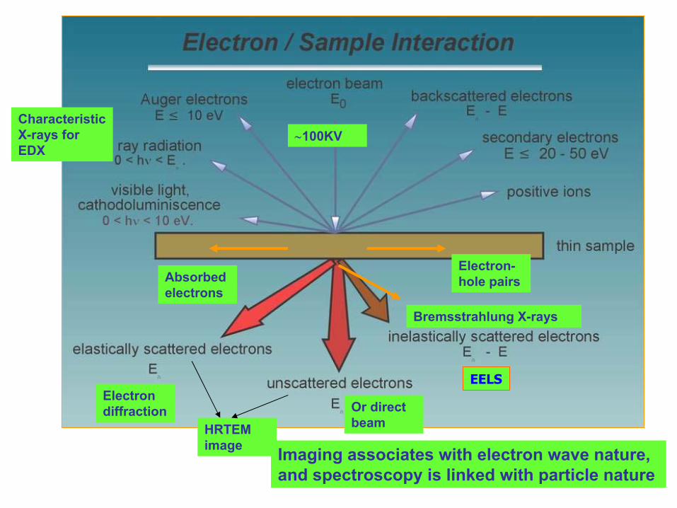
What happens when an energetic electron (100-400kv) strikes the specimen? Mostly, consider electron particle nature
Direction changes, but electron energy does not
≤10°
The electron energy changes, but the direction does not change much (∼0.1°)
CHEM 793, 2011 Fall
∼100KV
Or direct beam
Electron diffraction
Absorbed electrons
Electron-hole pairs
Bremsstrahlung X-rays
Characteristic X-rays for EDX
EELS
HRTEM image Imaging associates with electron wave nature,
and spectroscopy is linked with particle nature

CHEM 793, 2011 Fall
The Interaction Cross-section
The interaction cross-section, σ, is the probability that a scattering process will occur
areaunit particles/incident ofnumber n nit volume targets/uofnumber n
t volumeevents/uni ofnumber N :where
i
t
===
=tinn
Nσ
Unit of cross-section: 1 barn=1x10-24 cm2
CHEM 793, 2011 Fall
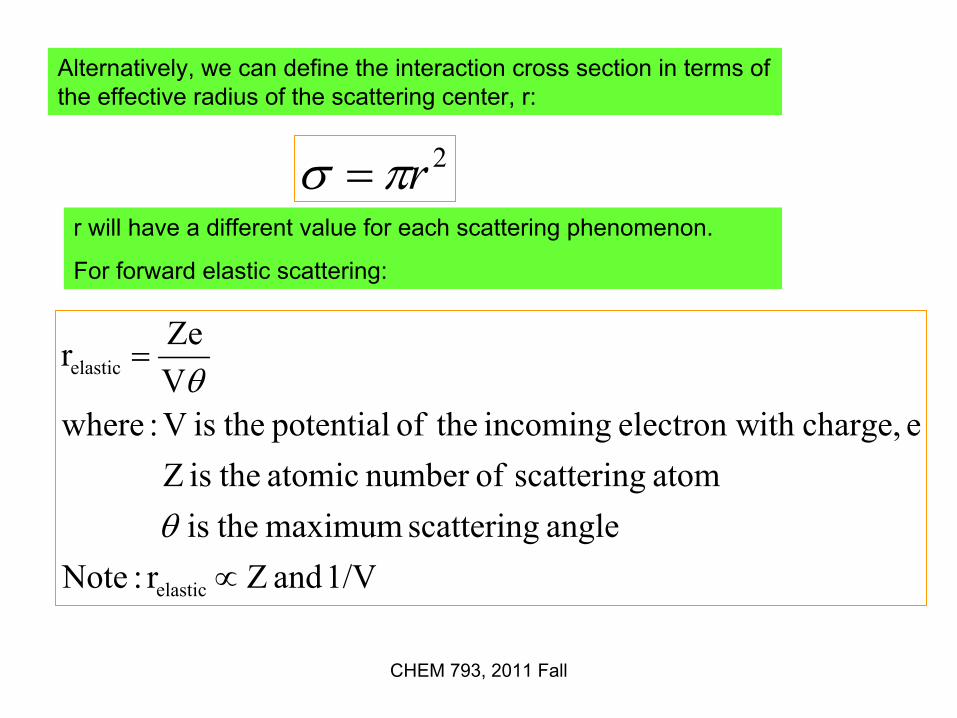
Alternatively, we can define the interaction cross section in terms of the effective radius of the scattering center, r:
2rπσ =r will have a different value for each scattering phenomenon.
For forward elastic scattering:
1/V and Z r :Noteangle scattering maximum theis
atom scattering ofnumber atomic theis Z e charge,ith electron w incoming theof potential theis V :where
VZer
elastic
elastic
∝
=
θ
θ
CHEM 793, 2011 Fall
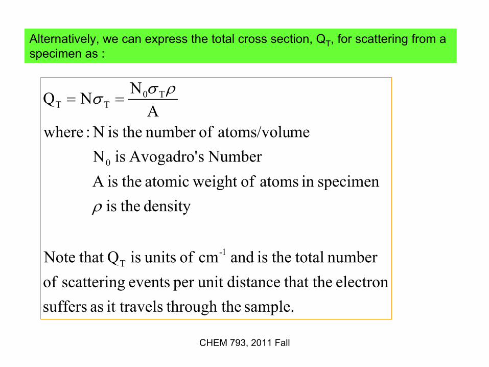
Alternatively, we can express the total cross section, QT, for scattering from a specimen as :
sample. he through tit travels as sufferselectron that thedistanceunit per events scattering of
number total theis and cm of units is Q that Note
density theis specimenin atoms of weight atomic theisA
Number sAvogadro' is N meatoms/volu ofnumber theis N :where
ANNQ
1-T
0
T0TT
ρ
ρσσ ==

CHEM 793, 2011 Fall
If we have a specimen of thickness, t, the probability of scattering from that specimen is:
( )A
tNtQ TT
ρσ0=
The product (ρt) is called the mass-thickness, which governs the image contrast of bio-sample and polymer, etc.
Note:
• typical small-angle elastic cross-section in metals are ~10-22 m2 (10-18 cm2)
• Inelastic cross sections range from 10-22 m2 (1,000,000 barns) to 10-26 m2
(100 barns) depending on the material and the type of scattering.
CHEM 793, 2011 Fall
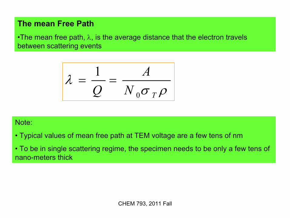
The mean Free Path•The mean free path, λ, is the average distance that the electron travels between scattering events
ρσλ
TNA
Q 0
1==
Note:
• Typical values of mean free path at TEM voltage are a few tens of nm
• To be in single scattering regime, the specimen needs to be only a few tens of nano-meters thick
CHEM 793, 2011 Fall
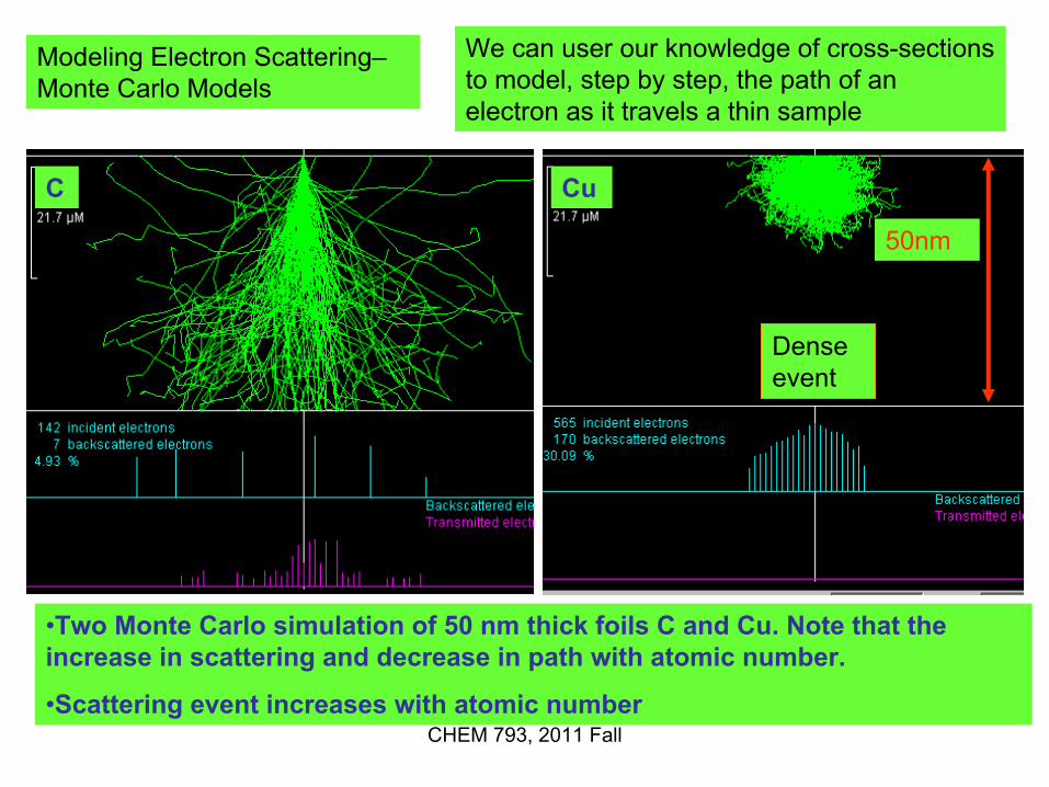
•Two Monte Carlo simulation of 50 nm thick foils C and Cu. Note that the increase in scattering and decrease in path with atomic number.
•Scattering event increases with atomic number
C Cu
50nm
Modeling Electron Scattering–Monte Carlo Models
We can user our knowledge of cross-sections to model, step by step, the path of an electron as it travels a thin sample
Dense event

CHEM 793, 2011 Fall
Interaction with the electron cloud gives rise to a low angle electron-electron scattering events
cloudelectron theof radius theis r where e
22
==
θππσVereelectron
Interaction with the atomic nucleus gives rise to a high angle electron-nucleus scattering events
nucleus atomic theof radius theis r where n
22
==
θππσVZernelectron
Z and θ control TEM image contrast
Nucleus
θ
θ
Electron cloud
Two mechanism of e- scattering
•Coulombic interaction: low angle
•Coulombic attraction: high angle and even complete backscatter

CHEM 793, 2011 Fall
The Rutherford Cross-section for Scattering
The total elastic cross-section in events per electron per atom per m2 is
( ) ( ) ( )θθθ
θσ
tan1tancocot
2cot
EZ1062.1 2
2
0
24nucleus
=−=
×= −
This equation can be modified to account for scattering by atoms in a TEM specimen of thickness, t:
×=
= −
2cot1062.1 2
2
00
240
θρσρEZt
ANt
ANtQnucleus
Note that (ρt) dependence and the strong dependence on Z and the beam energy, E0
CHEM 793, 2011 Fall
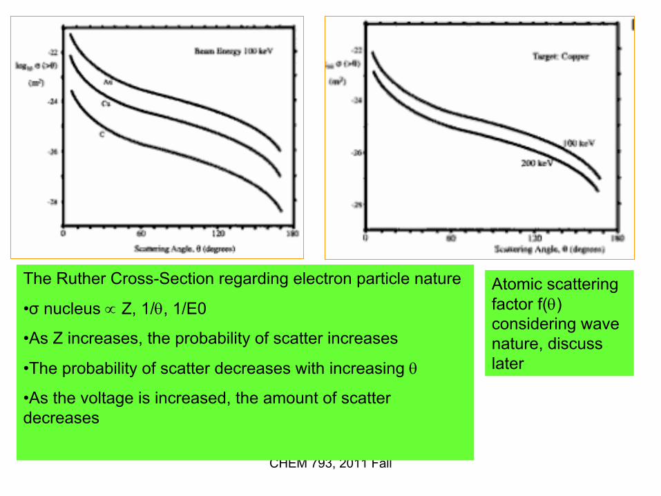
The Ruther Cross-Section regarding electron particle nature
•σ nucleus ∝ Z, 1/θ, 1/E0
•As Z increases, the probability of scatter increases
•The probability of scatter decreases with increasing θ
•As the voltage is increased, the amount of scatter decreases
Atomic scattering factor f(θ) considering wave nature, discuss later

CHEM 793, 2011 Fall
The Ruther Cross-Section can be converted to a mean free path
•Note: As the atomic number increases, the mean-free path decreases
•As the voltage is increased, the mean free path increases

CHEM 793, 2011 Fall
Inelastic scattering1.Single electron excitations:
•Low energy secondary electrons: used for SEM imaging
•Fast Electron secondary electrons: carries up to half the beam energy, degrade resolution
•Inner shell ionization: emission of characteristic X-rays or Auger electrons
2. Many Electron Excitations:
•Continuum X-ray production; background X-ray spectrum
•Plasmon scattering: oscillation of loosely bound electrons
•Phonon scattering: atomic lattice vibration
CHEM 793, 2011 Fall
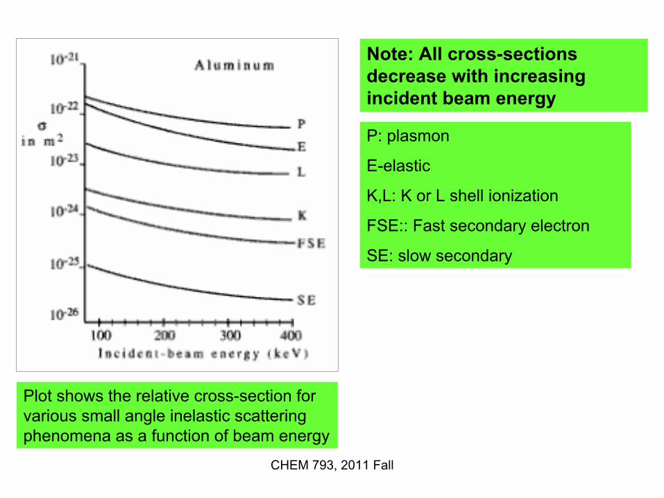
Plot shows the relative cross-section for various small angle inelastic scattering phenomena as a function of beam energy
P: plasmon
E-elastic
K,L: K or L shell ionization
FSE:: Fast secondary electron
SE: slow secondary
Note: All cross-sections decrease with increasing incident beam energy

CHEM 793, 2011 Fall
Characteristic X-ray Generation
Incident electrons E0
( ) ( )LEKEhv −=energy ofphoton ray -X
Transmitted electrons E0 –E
Where E is the binding energy of electron

CHEM 793, 2011 Fall
Energy (keV)
Cou
nts
20100
600
400
200
0
CO
Al
CaCa
SrSrSr
Ti
Ti CuCu 500 nm
1
EDX showing the elements distribution of aluminum Silica waste form loaded with Cs/Sr
• no sub-shell excitation information

CHEM 793, 2011 Fall
Energy (keV)
Cou
nts
20100
600
400
200
0
Kα1
OKα1
AlKα1
CaKα1
CaKβ1
SrKα1
SrKβ1
SrKβ2TiKα1
CuKα1
CuKβ1500 nm
1
EDX showing the elements distribution of aluminum silica waste form loaded with Cs/Sr
• with sub-shell excitation information
• how to label the sub-shell excitation?
CHEM 793, 2011 Fall
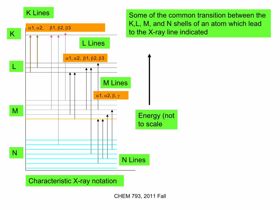
K Lines
α1, α2, β1, β2, β3
L Lines
M Lines
N Lines
α1, α2, β1, β2, β3
α1, α2, β, γ
K
L
M
N
Some of the common transition between the K,L, M, and N shells of an atom which lead to the X-ray line indicated
Characteristic X-ray notation
Energy (not to scale
CHEM 793, 2011 Fall
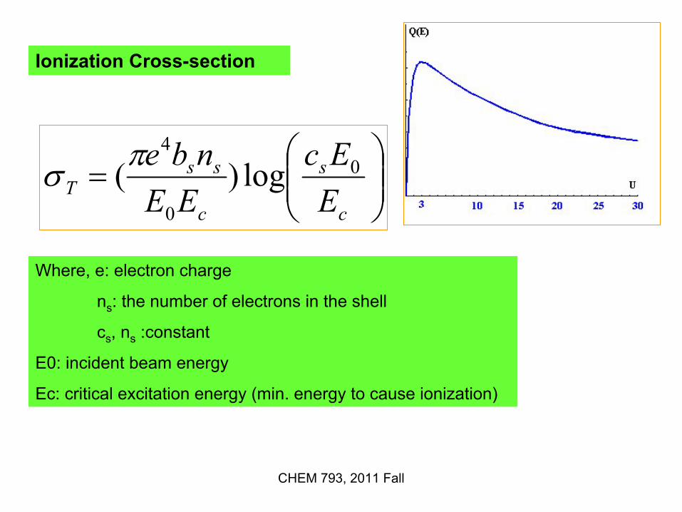
Ionization Cross-section
=
c
s
c
ssT E
EcEEnbe 0
0
4
log)(πσ
Where, e: electron charge
ns: the number of electrons in the shell
cs, ns :constant
E0: incident beam energy
Ec: critical excitation energy (min. energy to cause ionization)
CHEM 793, 2011 Fall
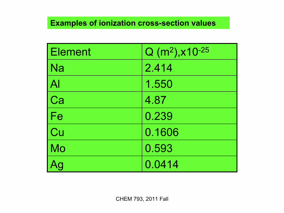
Examples of ionization cross-section values
0.0414Ag0.593Mo0.1606Cu0.239Fe4.87Ca1.550Al2.414NaQ (m2),x10-25Element

CHEM 793, 2011 Fall
Fluorescence Yield (ω): the probability of the X-ray versus Auger emission
4
4
ZaZ+
=ωWhere:
Z: atomic number; A: constant ~106
Carbon 10-3;Germanium: 0.5
Increasing X-ray emission
Increasing Auger e emission
CHEM 793, 2011 Fall
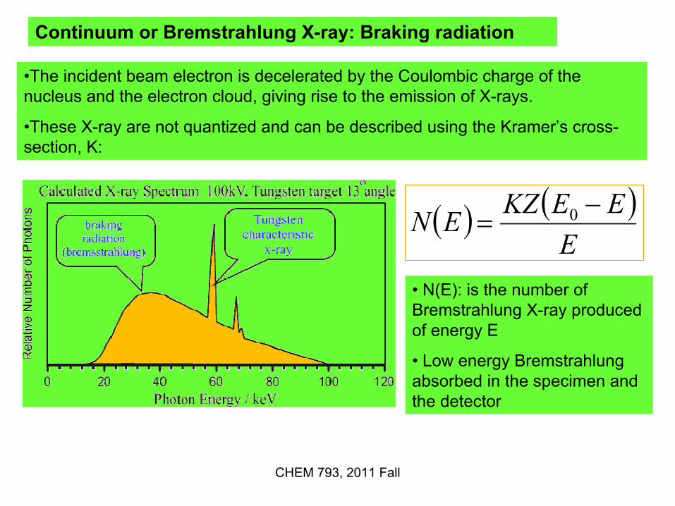
Continuum or Bremstrahlung X-ray: Braking radiation
•The incident beam electron is decelerated by the Coulombic charge of the nucleus and the electron cloud, giving rise to the emission of X-rays.
•These X-ray are not quantized and can be described using the Kramer’s cross-section, K:
( ) ( )E
EEKZEN −= 0
• N(E): is the number of Bremstrahlung X-ray produced of energy E
• Low energy Bremstrahlungabsorbed in the specimen and the detector
CHEM 793, 2011 Fall
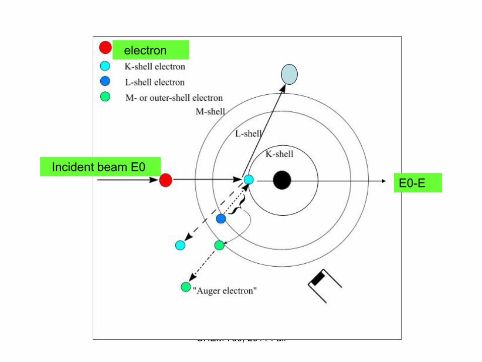
Secondary Electrons
SEs are simply electrons in the specimen that are ejected by the beam electrons. Three are types of SE:
• Elected conduction or balance band electron produce slow secondaries with energy below 50 eV, These electrons are used for SEM imaging.
• Ejected inner shell electrons are more strongly bound and produce higher energy secondary electron, fast secondaries, with up to half the incident beam energy.
• A outer electron falls into the inner shell vacancy created by an ionization event, and a second electron, the Auger electron, is emitted carrying off the excess energy.
CHEM 793, 2011 Fall
Incident beam E0
electron
E0-E

CHEM 793, 2011 Fall
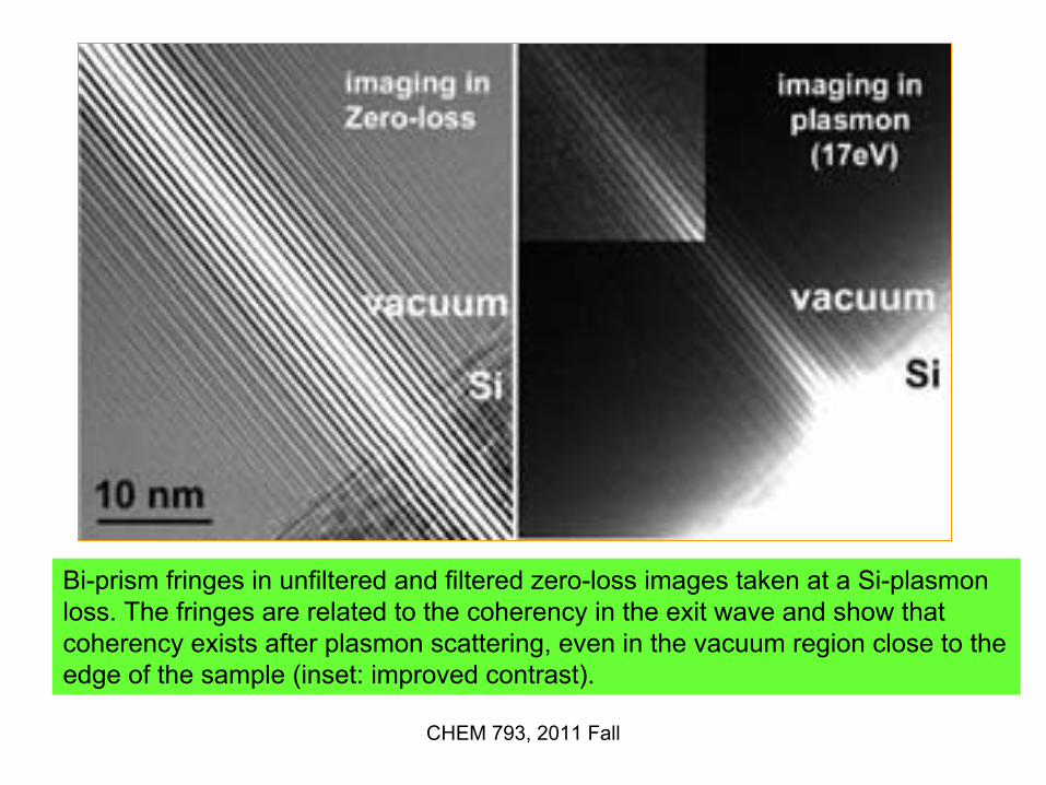
Plasmons
Plasmons are collective oscillations of free electrons that occur when the beam electron passes through the free electron gas.
•Plasmon energy is quantized.
•Plasmon energy also changes with electron density which depends on the local composition of the sample. Plasmon may be used for microanalysis through energy loss imaging to help to focus image
The mean free path for plasmon excitation is about 100nm. This can be used for measuring sample thickness
CHEM 793, 2011 Fall
Bi-prism fringes in unfiltered and filtered zero-loss images taken at a Si-plasmonloss. The fringes are related to the coherency in the exit wave and show that coherency exists after plasmon scattering, even in the vacuum region close to the edge of the sample (inset: improved contrast).
CHEM 793, 2011 Fall
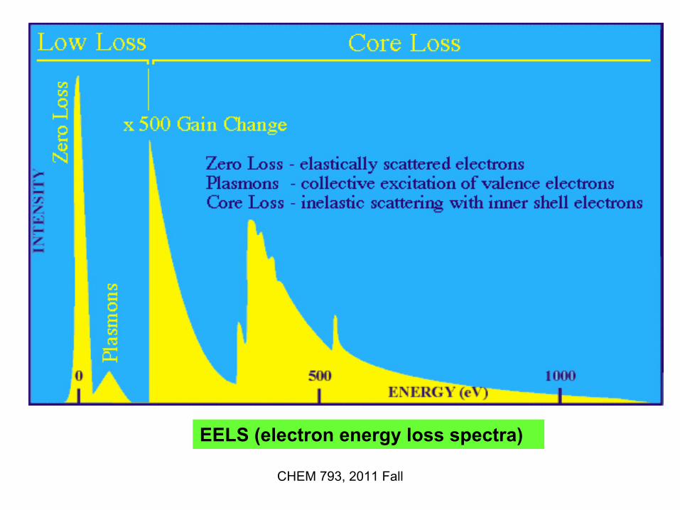
EELS (electron energy loss spectra)

CHEM 793, 2011 Fall
Phonons
•Bonds vibrate when struck by high energy electrons creating lattice oscillations -essentially equivalent to heating the sample
•Phonons are responsible for the thermal diffuse scattering observed around electron diffracting pattern spots. Sample cooling reduces this effect.
•The mean free path for phonon excitation is 350 nm for Al and only a few nm for Au

CHEM 793, 2011 Fall
Diffuse zone in electron diffraction pattern

CHEM 793, 2011 Fall
Typical ED patterns in SiO grains at 500, 750 and 1000 °C respectively. Diffuse rings became sharper in spite of the high temperature. The diffraction rings can be identified as those of Si and cristobalite
CHEM 793, 2011 Fall
Beam DamageThere are two types of e-beam damage
• Radiolysis: inelastic scatting (mainly heating of the sample) breaks the chemical binds of certain materials. For example. SiO2 is easily damage through radiolysis in a 300 kv TEM. Polymers and ceramics also easily are subjected to radiolysis.
• Good thermal contact between the sample and the stage can reduce electron beam heating of the sample. Higher operation voltages minimize heat transfer
• Knock on damage: direct displacement of atoms from the crystal lattice creating points defects. It is directly related to the beam energy
CHEM 793, 2011 Fall
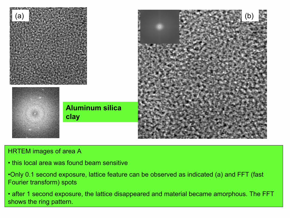
HRTEM images of area A
• this local area was found beam sensitive
•Only 0.1 second exposure, lattice feature can be observed as indicated (a) and FFT (fast Fourier transform) spots
• after 1 second exposure, the lattice disappeared and material became amorphous. The FFT shows the ring pattern.
(a) (b)
Aluminum silica clay

CHEM 793, 2011 Fall
STEM images prior and post convergent beam exposure for 2 minutes showing beam sensitive
(a) Prior to beam exposure
(b) After exposure, the spots were observed as indicated
(a) (b)
CHEM 793, 2011 Fall
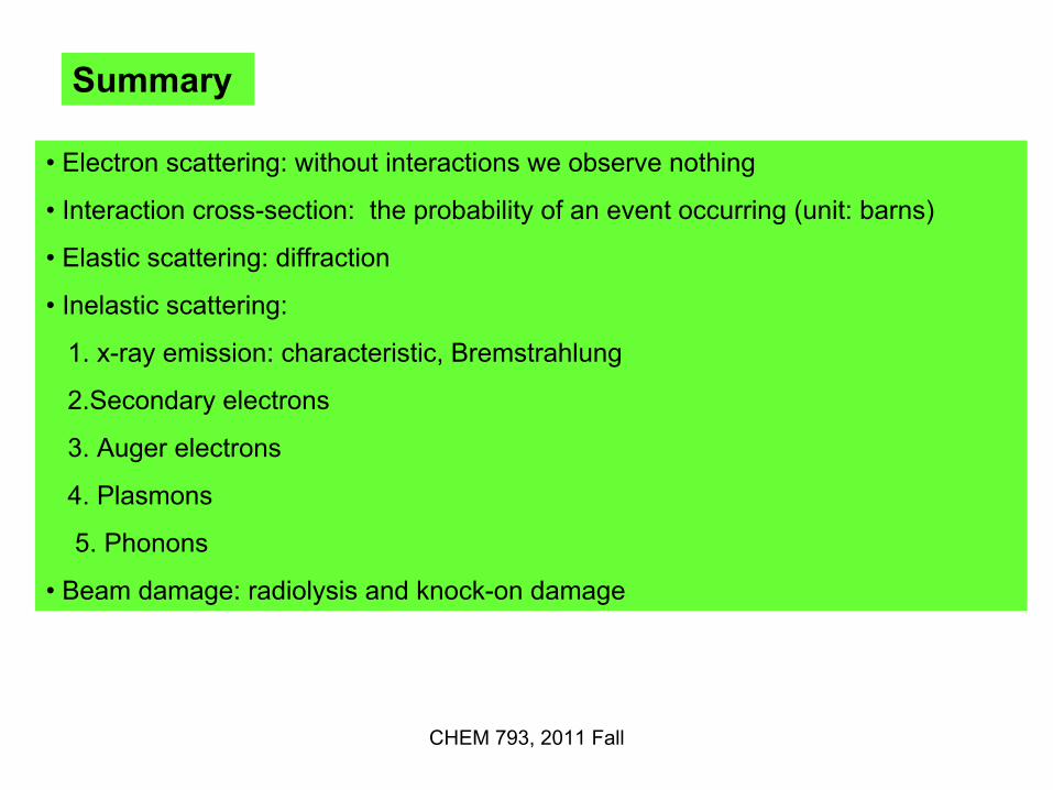
Summary
• Electron scattering: without interactions we observe nothing
• Interaction cross-section: the probability of an event occurring (unit: barns)
• Elastic scattering: diffraction
• Inelastic scattering:
1. x-ray emission: characteristic, Bremstrahlung
2.Secondary electrons
3. Auger electrons
4. Plasmons
5. Phonons
• Beam damage: radiolysis and knock-on damage
CHEM 793, 2011 Fall
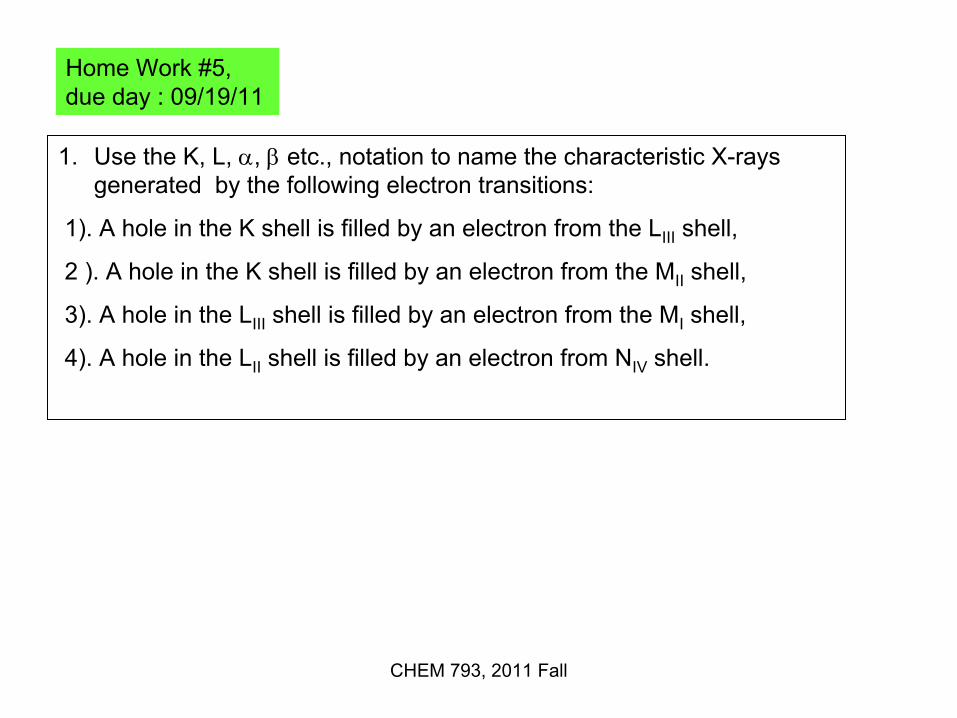
Home Work #5, due day : 09/19/11
1. Use the K, L, α, β etc., notation to name the characteristic X-rays generated by the following electron transitions:
1). A hole in the K shell is filled by an electron from the LIII shell,
2 ). A hole in the K shell is filled by an electron from the MII shell,
3). A hole in the LIII shell is filled by an electron from the MI shell,
4). A hole in the LII shell is filled by an electron from NIV shell.

CHEM 793, 2011 Fall
Home Work #6 due day : 09/19/11
For materials of known composition, a semi-empirical equation can calculate the mean free path using a TEM sample.
( )
:givenfactor icrelativist a is F ev loss,enery mean a is E keV energy,incident theis E
mrad semianle, collection theis where,
,/2ln
106
m
0
0
0
ββ
λmm EE
EEF
≈
20
0
5111
10221
+
+=
E
EF
For specimen of average atomic number, Z
36.06.7 ZEm ≈
Cont’

CHEM 793, 2011 Fall
Home Work #6, cont’
Problem:
(a) Using the equation shown above, plot the mean free path, λ, for inelastic scattering of electrons in Cu with an accelerating potential of 200 KV as a function of collection angles, β, ranging from 0.1 to 20 mrad.
(b). Using the same equations, plot the inelastic mean free path, λ, as a function of the average atomic number of a material Z with collection angles of 1.0, 5.0, 10.0, 15.0 and 20.0 mrad. Explain the graphs.