chapter 07 diagnosis slides 091806 - elsevierbooksite.elsevier.com/9780123705976/errata/12~chapter...
TRANSCRIPT
EE141
1
VLSI Test Principles and Architectures Ch. 7 - Logic Diagnosis - P. 1
Chapter 7Chapter 7
Logic DiagnosisLogic Diagnosis
EE141
2
VLSI Test Principles and Architectures Ch. 7 - Logic Diagnosis - P. 2
OutlineOutline
� Introduction
� Combinational Logic Diagnosis
� Scan Chain Diagnosis
� Logic BIST Diagnosis
� Conclusion
EE141
3
VLSI Test Principles and Architectures Ch. 7 - Logic Diagnosis - P. 3
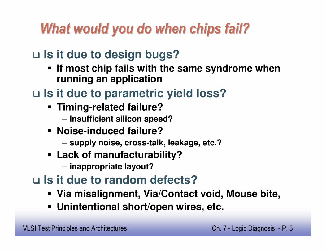
What would you do when chips fail?What would you do when chips fail?
� Is it due to design bugs?� If most chip fails with the same syndrome when
running an application
� Is it due to parametric yield loss?� Timing-related failure?
– Insufficient silicon speed?
� Noise-induced failure?– supply noise, cross-talk, leakage, etc.?
� Lack of manufacturability?– inappropriate layout?
� Is it due to random defects?� Via misalignment, Via/Contact void, Mouse bite,
� Unintentional short/open wires, etc.
EE141
4
VLSI Test Principles and Architectures Ch. 7 - Logic Diagnosis - P. 4
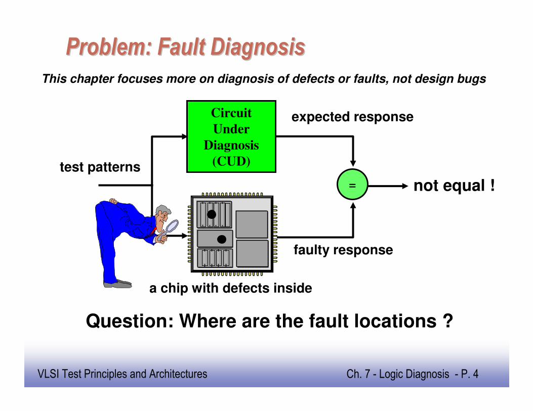
Problem: Fault DiagnosisProblem: Fault Diagnosis
Circuit
Under
Diagnosis
(CUD)test patterns
=
expected response
faulty response
not equal !
Question: Where are the fault locations ?
a chip with defects inside
This chapter focuses more on diagnosis of defects or faults, not design bugs
EE141
5
VLSI Test Principles and Architectures Ch. 7 - Logic Diagnosis - P. 5
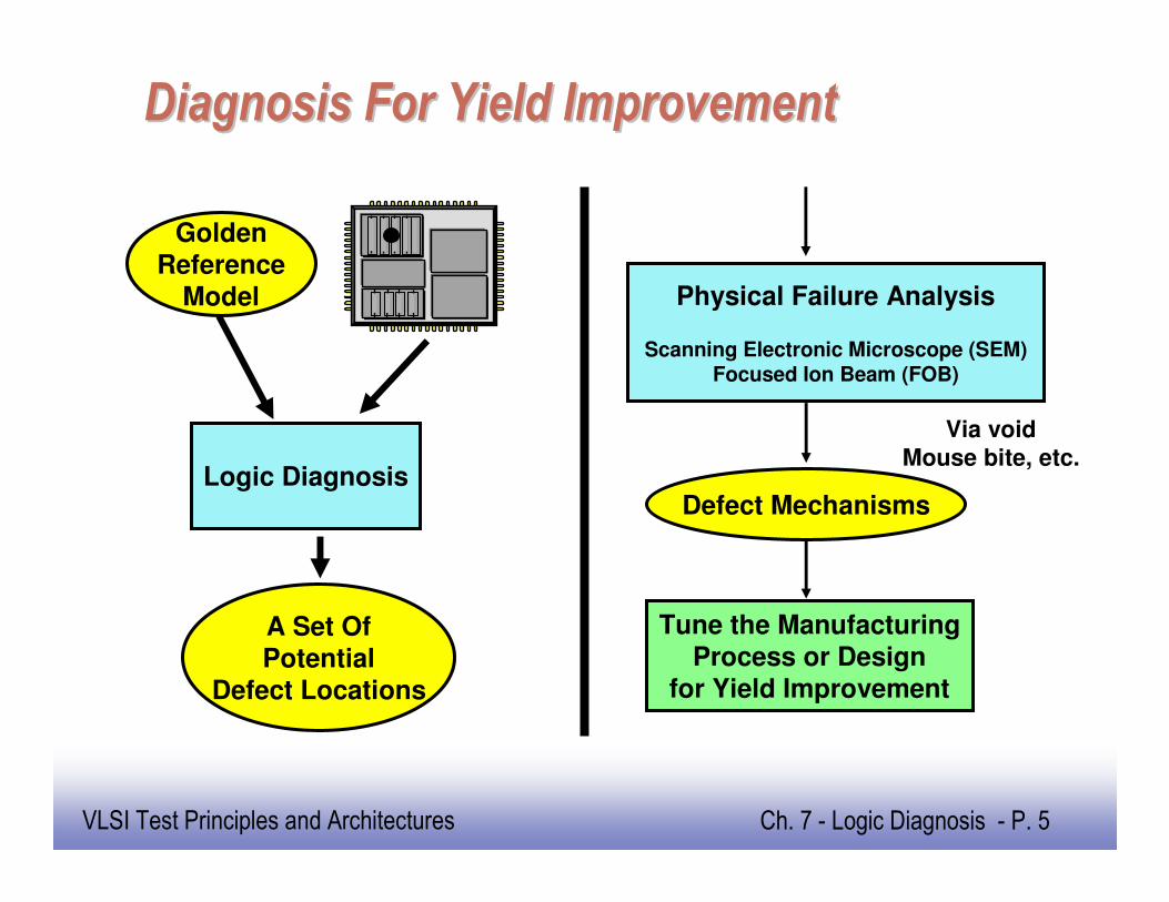
Diagnosis For Yield ImprovementDiagnosis For Yield Improvement
Logic DiagnosisDefect Mechanisms
A Set OfPotential
Defect Locations
GoldenReference
Model Physical Failure Analysis
Scanning Electronic Microscope (SEM)Focused Ion Beam (FOB)
Tune the ManufacturingProcess or Design
for Yield Improvement
Via voidMouse bite, etc.
EE141
6
VLSI Test Principles and Architectures Ch. 7 - Logic Diagnosis - P. 6
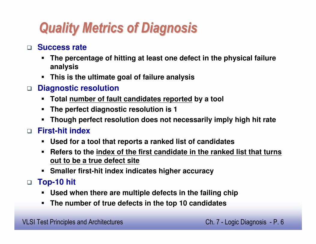
Quality Metrics of DiagnosisQuality Metrics of Diagnosis
� Success rate
� The percentage of hitting at least one defect in the physical failure analysis
� This is the ultimate goal of failure analysis
� Diagnostic resolution
� Total number of fault candidates reported by a tool
� The perfect diagnostic resolution is 1
� Though perfect resolution does not necessarily imply high hit rate
� First-hit index
� Used for a tool that reports a ranked list of candidates
� Refers to the index of the first candidate in the ranked list that turns out to be a true defect site
� Smaller first-hit index indicates higher accuracy
� Top-10 hit
� Used when there are multiple defects in the failing chip
� The number of true defects in the top 10 candidates
EE141
7
VLSI Test Principles and Architectures Ch. 7 - Logic Diagnosis - P. 7
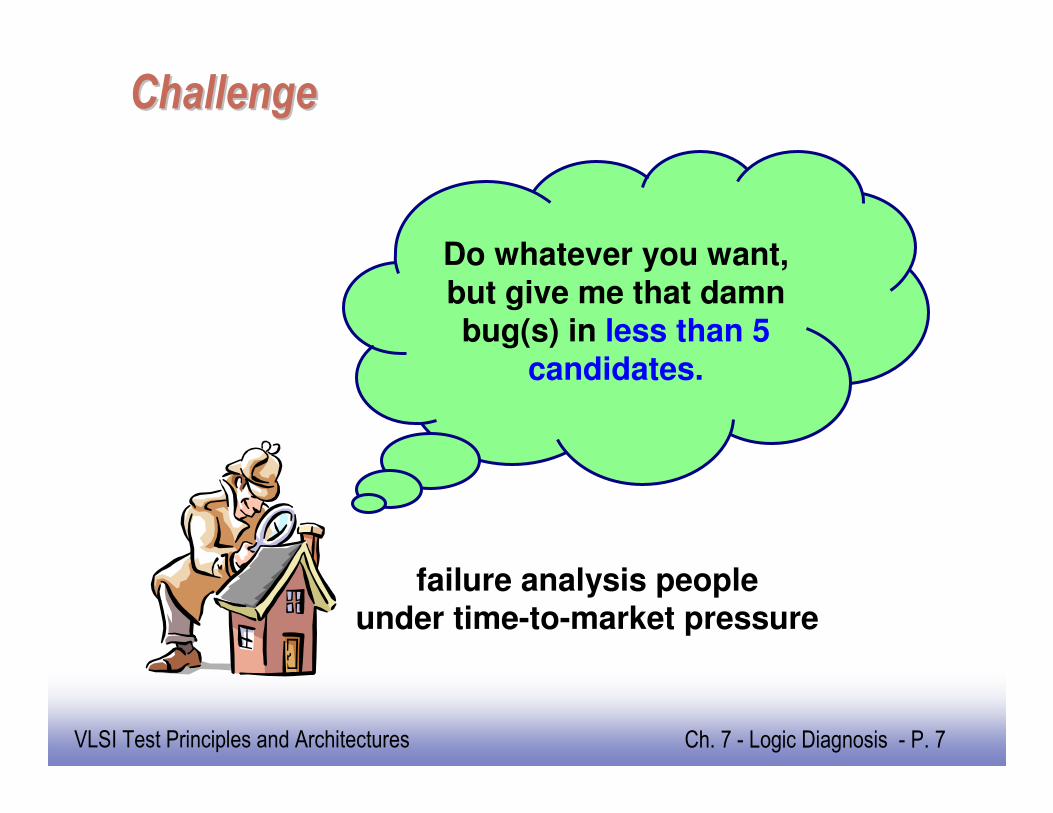
ChallengeChallenge
Do whatever you want,but give me that damn bug(s) in less than 5
candidates.
failure analysis peopleunder time-to-market pressure
EE141
8
VLSI Test Principles and Architectures Ch. 7 - Logic Diagnosis - P. 8
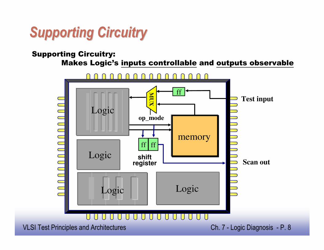
Supporting CircuitrySupporting Circuitry
memory
Scan out
MU
X
ff
op_mode
Logic
Logic
Logic
Logic
Test input
Supporting Circuitry:
Makes Logic’s inputs controllable and outputs observable
ff ff
shiftregister

EE141
9
VLSI Test Principles and Architectures Ch. 7 - Logic Diagnosis - P. 9
Design For DiagnosisDesign For Diagnosis
More Supporting Circuitry
Complexity
Of
Diagnosis
Original
Design
Separated
Logic &
Memory
interface circuitry
Logic Design
With Full-Scan
Scan-chain
EE141
10
VLSI Test Principles and Architectures Ch. 7 - Logic Diagnosis - P. 10
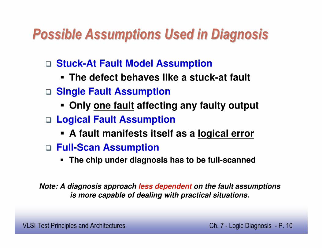
Possible Assumptions Used in DiagnosisPossible Assumptions Used in Diagnosis
� Stuck-At Fault Model Assumption
� The defect behaves like a stuck-at fault
� Single Fault Assumption
� Only one fault affecting any faulty output
� Logical Fault Assumption
� A fault manifests itself as a logical error
� Full-Scan Assumption
� The chip under diagnosis has to be full-scanned
Note: A diagnosis approach less dependent on the fault assumptions
is more capable of dealing with practical situations.

EE141
11
VLSI Test Principles and Architectures Ch. 7 - Logic Diagnosis - P. 11
Examples of FaultsExamples of Faults
� Node Fault
VDD
A
B A
bridging
GND
C
� Short Fault (Bridging)
Most diagnosis algorithms performs
at the gate level, trying to identify the
troubling signals or cells
αααα
ββββ
γγγγ
EE141
12
VLSI Test Principles and Architectures Ch. 7 - Logic Diagnosis - P. 12
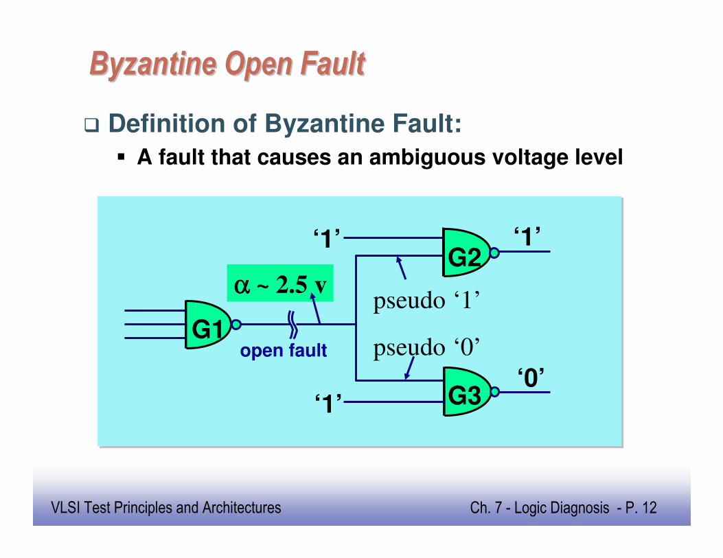
Byzantine Open FaultByzantine Open Fault
� Definition of Byzantine Fault:
� A fault that causes an ambiguous voltage level
αααα ~ 2.5 vG2
G3
‘1’
‘1’
‘1’
‘0’
pseudo ‘0’
pseudo ‘1’
open faultG1
EE141
13
VLSI Test Principles and Architectures Ch. 7 - Logic Diagnosis - P. 13
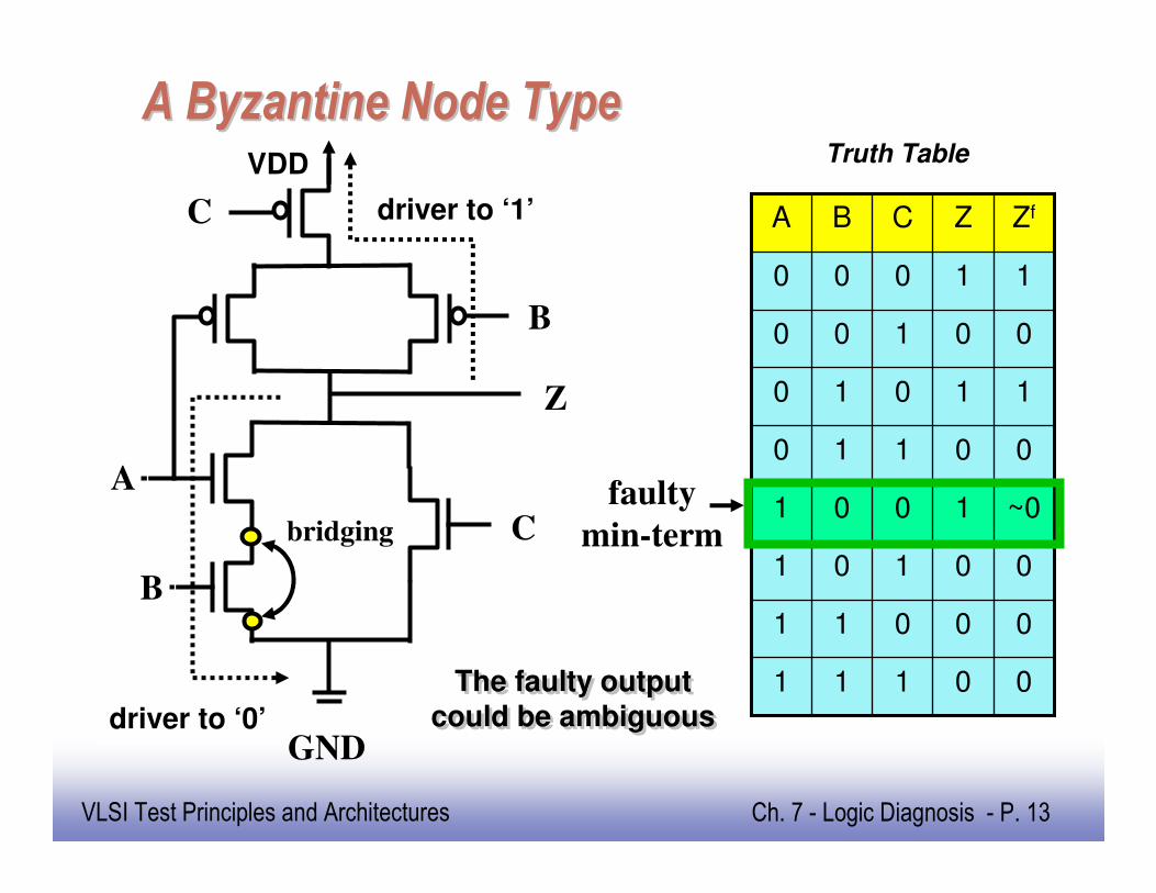
A Byzantine Node TypeA Byzantine Node Type
00111
00110
11010
00101
~01001
00011
00100
11000
ZfZCBA
faulty
min-term
C
A
bridging
GND
Z
B
C
B
VDD
driver to ‘0’
driver to ‘1’
The faulty outputcould be ambiguous
The faulty outputcould be ambiguous
Truth Table
EE141
14
VLSI Test Principles and Architectures Ch. 7 - Logic Diagnosis - P. 14
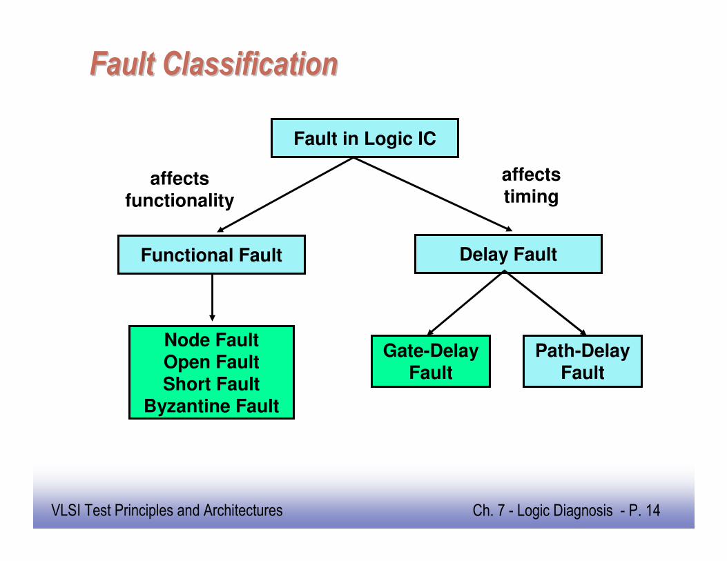
Fault ClassificationFault Classification
Fault in Logic IC
Functional Fault
Node FaultOpen FaultShort Fault
Byzantine Fault
affectsfunctionality
Delay Fault
Gate-DelayFault
Path-DelayFault
affectstiming
EE141
15
VLSI Test Principles and Architectures Ch. 7 - Logic Diagnosis - P. 15
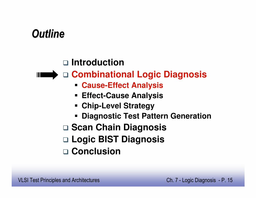
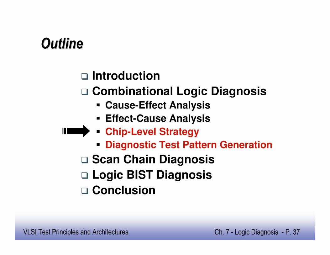
OutlineOutline
� Introduction
� Combinational Logic Diagnosis� Cause-Effect Analysis
� Effect-Cause Analysis
� Chip-Level Strategy
� Diagnostic Test Pattern Generation
� Scan Chain Diagnosis
� Logic BIST Diagnosis
� Conclusion

EE141
16
VLSI Test Principles and Architectures Ch. 7 - Logic Diagnosis - P. 16
TerminologyTerminology
� Device Under Diagnosis (DUD): The Failing Chip
� Circuit Under Diagnosis (CUD): The Circuit Model
� Failing Input Vector: Causes Mismatches
inputvector
v xooox
mismatched PO
matched PO
mismatched PO
matched PO
matched PO
Failing chip
Gate-level CUD
EE141
17
VLSI Test Principles and Architectures Ch. 7 - Logic Diagnosis - P. 17
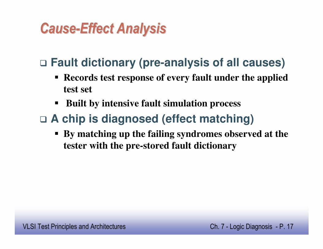
CauseCause--Effect AnalysisEffect Analysis
� Fault dictionary (pre-analysis of all causes)
� Records test response of every fault under the applied
test set
� Built by intensive fault simulation process
� A chip is diagnosed (effect matching)
� By matching up the failing syndromes observed at the
tester with the pre-stored fault dictionary
EE141
18
VLSI Test Principles and Architectures Ch. 7 - Logic Diagnosis - P. 18
Fault Dictionary ExampleFault Dictionary Example
Test vectors in terms of (a, b, c)Circuits
1
0
1
1
1
1
v5v4v3v2v1
0100f4
1001f3
f5
f2
f1
fault-free
0
1
0
0
1
1
1
0
1
1
1
0
0
0
1
0
(b) Full-response dictionary
a
bc
g
(a) Circuit under diagnosis
Circuit under
Diagnosis
(c) Diagnostic tree
{f1, f2, f3, f4, f5}
output=0v1
output=1
{f1, f4, f5}
0 1v2
f4
{f2, f3}
0 1v2
f2f3{f1, f5}
0 1v4
f1f5
A diagnosis session:
traverse from a path from root to a leaf
EE141
19
VLSI Test Principles and Architectures Ch. 7 - Logic Diagnosis - P. 19
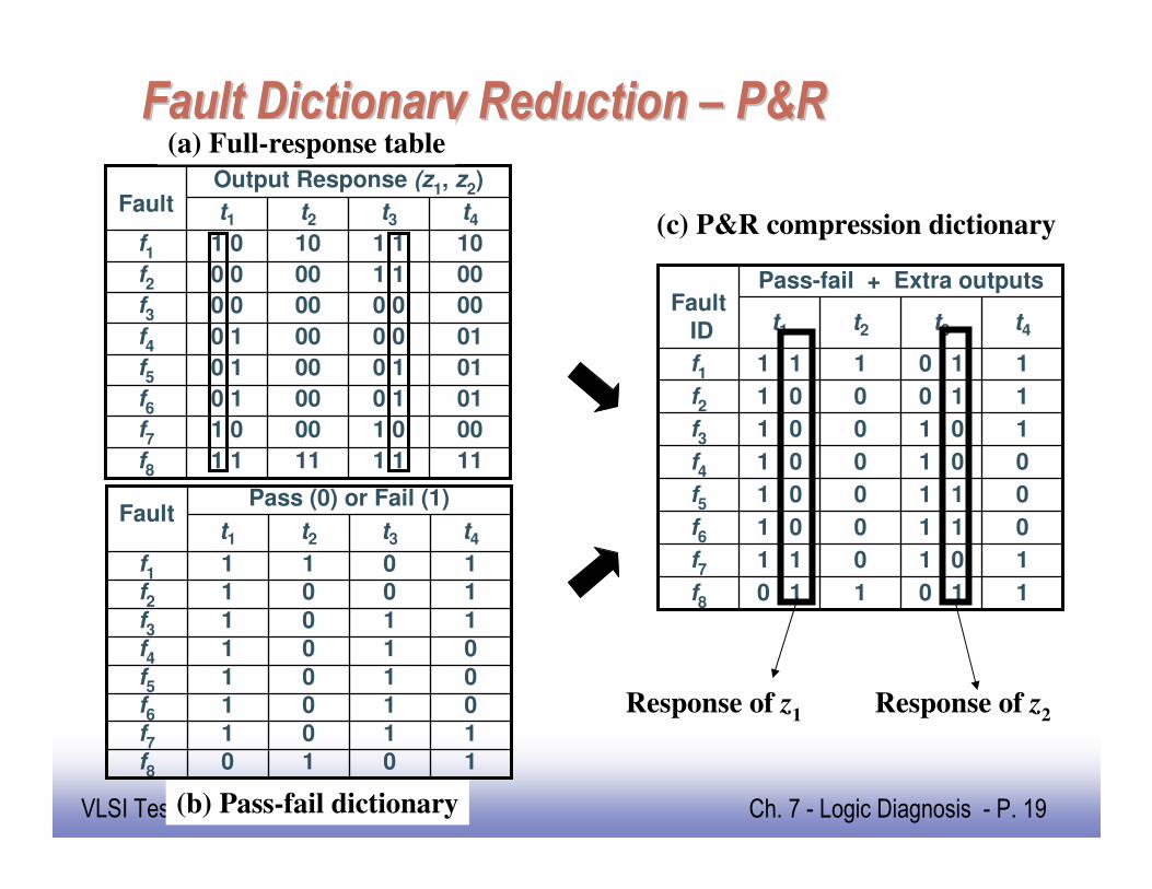
Fault Dictionary Reduction Fault Dictionary Reduction –– P&RP&R
Output Response (z1, z2)Fault
111 1111 1f8
010 1000 1f5
010 1000 1f6
001 0001 0f7
f4
f3
f2
f1
010 0000 1
0 0
0 0
1 0
t1
00
00
10
t2
0 0
1 1
1 1
t3
00
00
10
t4
(a) Full-response table
(b) Pass-fail dictionary
Pass (0) or Fail (1)Fault
1010f8
0101f5
0101f6
1101f7
f4
f3
f2
f1
0101
1
1
1
t1
0
0
1
t2
1
0
0
t3
1
1
1
t4
Pass-fail + Extra outputsFault
ID
10 110 1f8
01 101 0f5
01 101 0f6
11 001 1f7
f4
f3
f2
f1
01 0 01 0
1 0
1 0
1 1
t1
0
0
1
t2
1 0
0 1
0 1
t3
1
1
1
t4
(c) P&R compression dictionary
Response of z1
Response of z2
EE141
20
VLSI Test Principles and Architectures Ch. 7 - Logic Diagnosis - P. 20
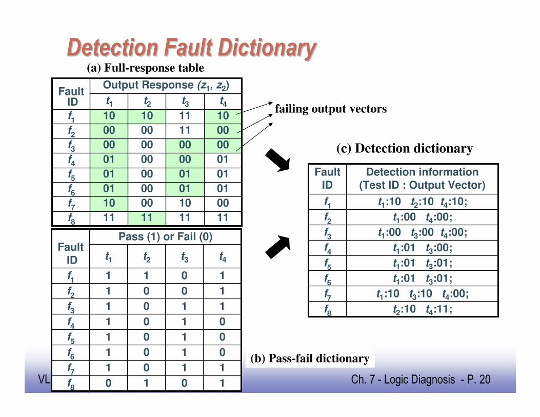
Detection Fault DictionaryDetection Fault Dictionary
Output Response (z1, z2)FaultID
11111111f8
01010001f5
01010001f6
00100010f7
f4
f3
f2
f1
01000001
00
00
10
t1
00
00
10
t2
00
11
11
t3
00
00
10
t4
(a) Full-response table
(b) Pass-fail dictionary
Pass (1) or Fail (0)Fault
ID
1010f8
0101f5
0101f6
1101f7
f4
f3
f2
f1
0101
1
1
1
t1
0
0
1
t2
1
0
0
t3
1
1
1
t4
t1:10 t2:10 t4:10;f1
t1:00 t4:00;f2
t1:00 t3:00 t4:00;f3
t1:01 t3:00;f4
t1:01 t3:01;f5
t1:01 t3:01;f6
t1:10 t3:10 t4:00;f7
t2:10 t4:11;f8
Detection information(Test ID : Output Vector)
FaultID
(c) Detection dictionary
failing output vectors
EE141
21
VLSI Test Principles and Architectures Ch. 7 - Logic Diagnosis - P. 21
OutlineOutline
� Introduction
� Combinational Logic Diagnosis� Cause-Effect Analysis
� Effect-Cause Analysis
� Chip-Level Strategy
� Diagnostic Test Pattern Generation
� Scan Chain Diagnosis
� Logic BIST Diagnosis
� Conclusion
EE141
22
VLSI Test Principles and Architectures Ch. 7 - Logic Diagnosis - P. 22
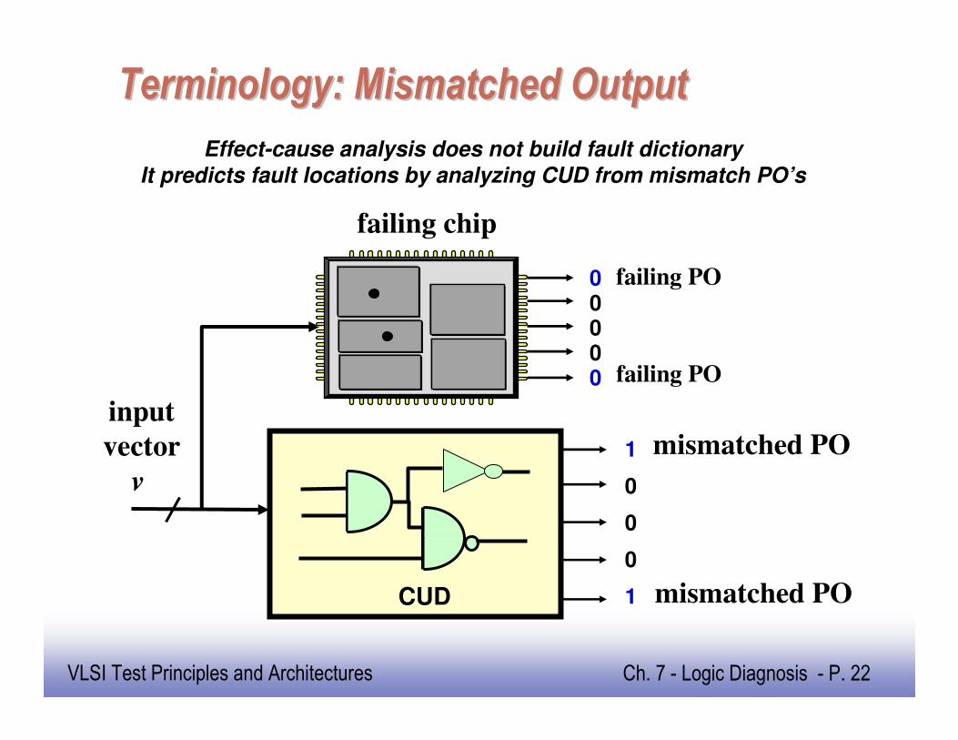
Terminology: Mismatched OutputTerminology: Mismatched Output
input
vector
v
00000
mismatched PO
mismatched POCUD
1
0
0
0
1
failing chip
failing PO
failing PO
Effect-cause analysis does not build fault dictionary
It predicts fault locations by analyzing CUD from mismatch PO’s
EE141
23
VLSI Test Principles and Architectures Ch. 7 - Logic Diagnosis - P. 23
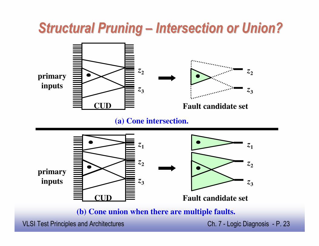
Structural Pruning Structural Pruning –– Intersection or Union?Intersection or Union?
(b) Cone union when there are multiple faults.
z1
z2
z3
z1
z2
z3
z2
z3
z2
z3
(a) Cone intersection.
primary
inputs
primary
inputs
Fault candidate set
Fault candidate setCUD
CUD
EE141
24
VLSI Test Principles and Architectures Ch. 7 - Logic Diagnosis - P. 24
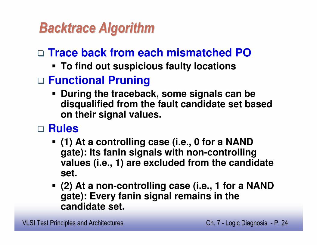
BacktraceBacktrace AlgorithmAlgorithm
� Trace back from each mismatched PO� To find out suspicious faulty locations
� Functional Pruning� During the traceback, some signals can be
disqualified from the fault candidate set based on their signal values.
� Rules� (1) At a controlling case (i.e., 0 for a NAND
gate): Its fanin signals with non-controlling values (i.e., 1) are excluded from the candidate set.
� (2) At a non-controlling case (i.e., 1 for a NAND gate): Every fanin signal remains in the candidate set.
EE141
25
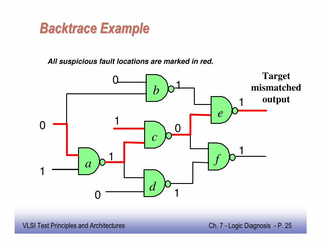
VLSI Test Principles and Architectures Ch. 7 - Logic Diagnosis - P. 25
BacktraceBacktrace ExampleExample
Target
mismatched
output1
1
10
1
0
0
1
1
0
1a
b
c
d
e
f
All suspicious fault locations are marked in red.
EE141
26
VLSI Test Principles and Architectures Ch. 7 - Logic Diagnosis - P. 26
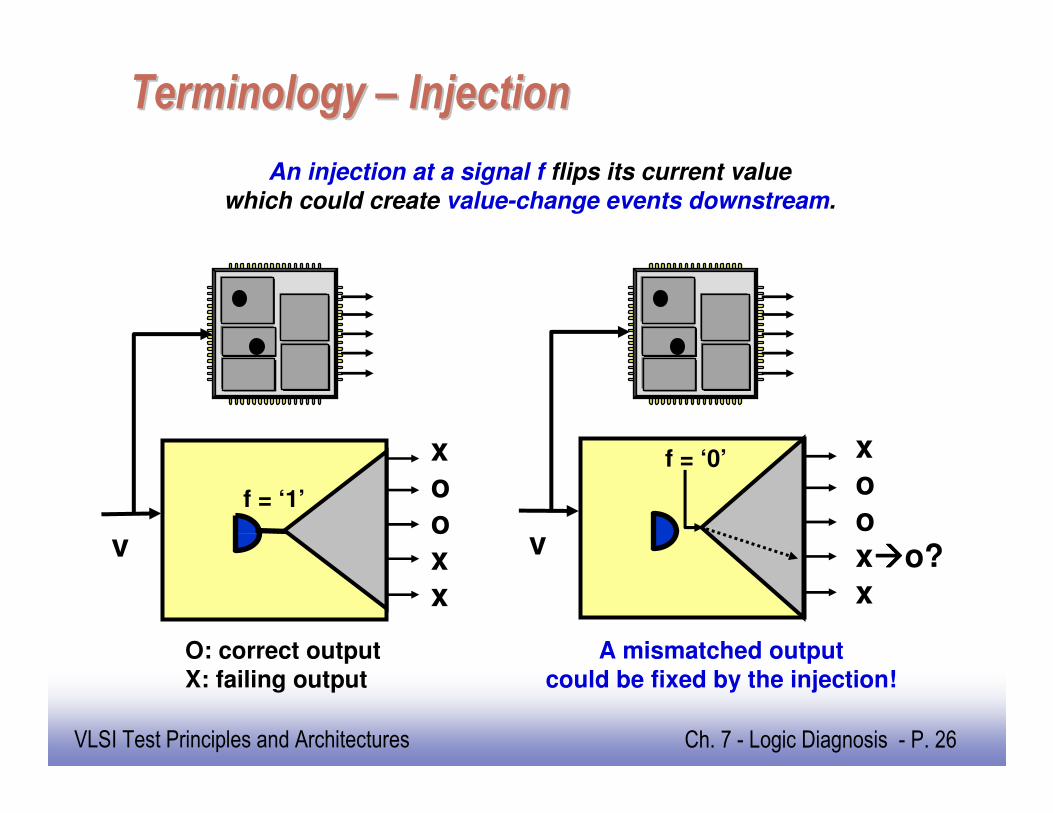
Terminology Terminology –– InjectionInjection
v
f = ‘1’
xooxx
v
f = ‘0’
A mismatched output
could be fixed by the injection!
An injection at a signal f flips its current value
which could create value-change events downstream.
O: correct output
X: failing output
xoox����o?x
EE141
27
VLSI Test Principles and Architectures Ch. 7 - Logic Diagnosis - P. 27
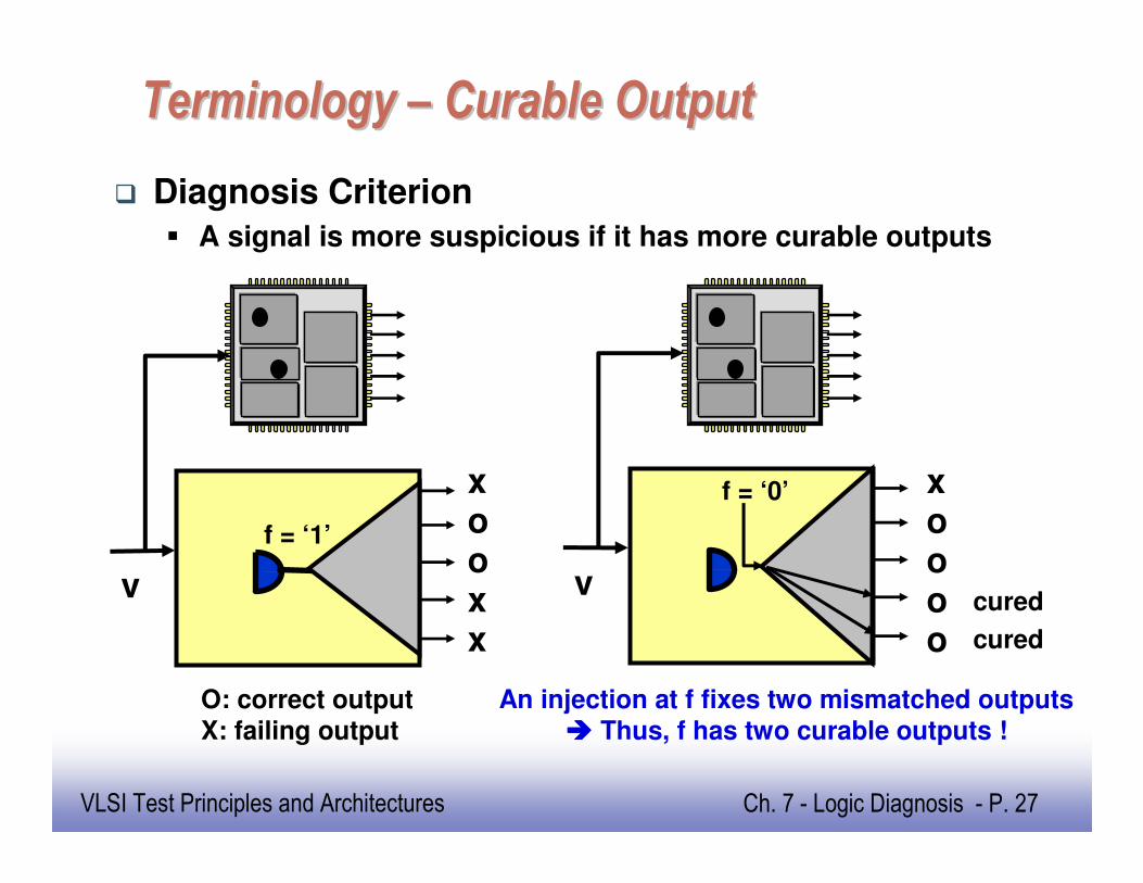
Terminology Terminology –– Curable OutputCurable Output
� Diagnosis Criterion
� A signal is more suspicious if it has more curable outputs
v
f = ‘1’
xooxx
v
f = ‘0’ xoooo
cured
cured
An injection at f fixes two mismatched outputs���� Thus, f has two curable outputs !
O: correct outputX: failing output
EE141
28
VLSI Test Principles and Architectures Ch. 7 - Logic Diagnosis - P. 28
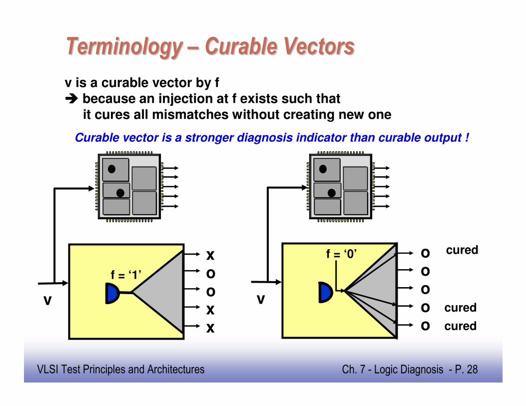
Terminology Terminology –– Curable VectorsCurable Vectors
v
f = ‘1’
xooxx
v
f = ‘0’ ooooo
cured
cured
cured
v is a curable vector by f���� because an injection at f exists such that
it cures all mismatches without creating new one
Curable vector is a stronger diagnosis indicator than curable output !
EE141
29
VLSI Test Principles and Architectures Ch. 7 - Logic Diagnosis - P. 29
Example of Curable VectorExample of Curable Vector
1
1
1
f1���� 0
01
0���� 1
10
1���� 0
x1
x2
x3
x4
cured
0
1
x1 = 0
x2 = 1
x3 = 1
x4 = 1
1
failing
(a) Failing Chip
(b) Circuit Under Diagnosis
EE141
30
VLSI Test Principles and Architectures Ch. 7 - Logic Diagnosis - P. 30
Why Curable Vector ?Why Curable Vector ?
� Information theory� A less probable event contains more information
� Curable output is an easy-to-satisfy criterion, high aliasing
� Curable vector is a hard-to-satisfy criterion, low aliasing
� Niche input vector
– Is an failing input vector that activates only one fault
– Likely to be a curable vector of certain signals
– Few, but tells more about the real fault locations
� Not all failing input vectors are equal !
EE141
31
VLSI Test Principles and Architectures Ch. 7 - Logic Diagnosis - P. 31
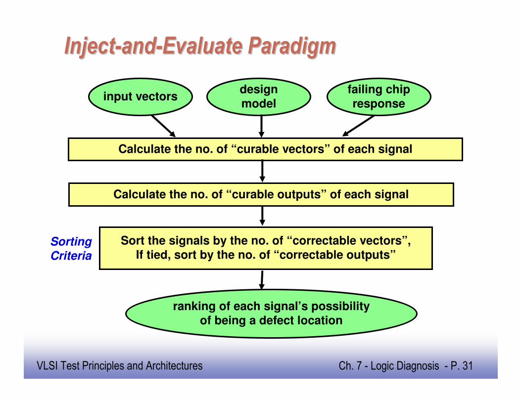
InjectInject--andand--Evaluate ParadigmEvaluate Paradigm
input vectorsdesign
model
failing chip
response
Calculate the no. of “curable vectors” of each signal
Calculate the no. of “curable outputs” of each signal
Sort the signals by the no. of “correctable vectors”,If tied, sort by the no. of “correctable outputs”
ranking of each signal’s possibilityof being a defect location
SortingCriteria
EE141
32
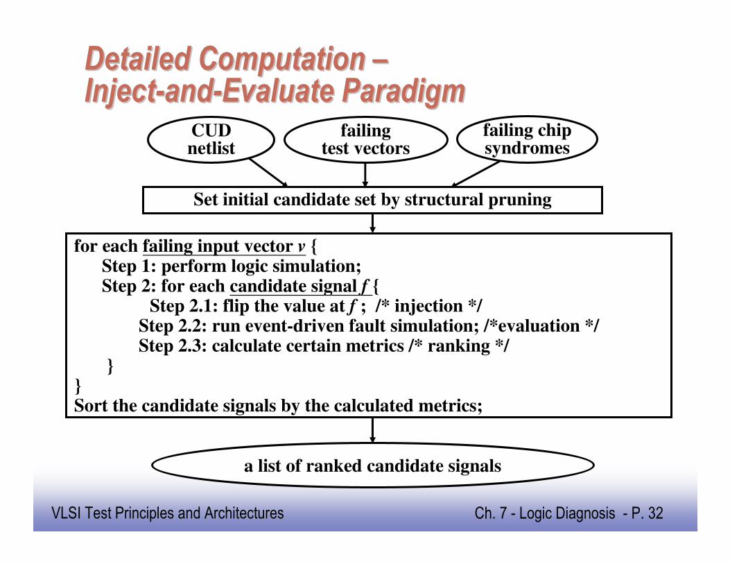
VLSI Test Principles and Architectures Ch. 7 - Logic Diagnosis - P. 32
Detailed Computation Detailed Computation ––InjectInject--andand--Evaluate ParadigmEvaluate Paradigm
CUDnetlist
failingtest vectors
failing chipsyndromes
Set initial candidate set by structural pruning
a list of ranked candidate signals
for each failing input vector v {Step 1: perform logic simulation;Step 2: for each candidate signal f {
Step 2.1: flip the value at f ; /* injection */Step 2.2: run event-driven fault simulation; /*evaluation */Step 2.3: calculate certain metrics /* ranking */
}}Sort the candidate signals by the calculated metrics;
EE141
33
VLSI Test Principles and Architectures Ch. 7 - Logic Diagnosis - P. 33
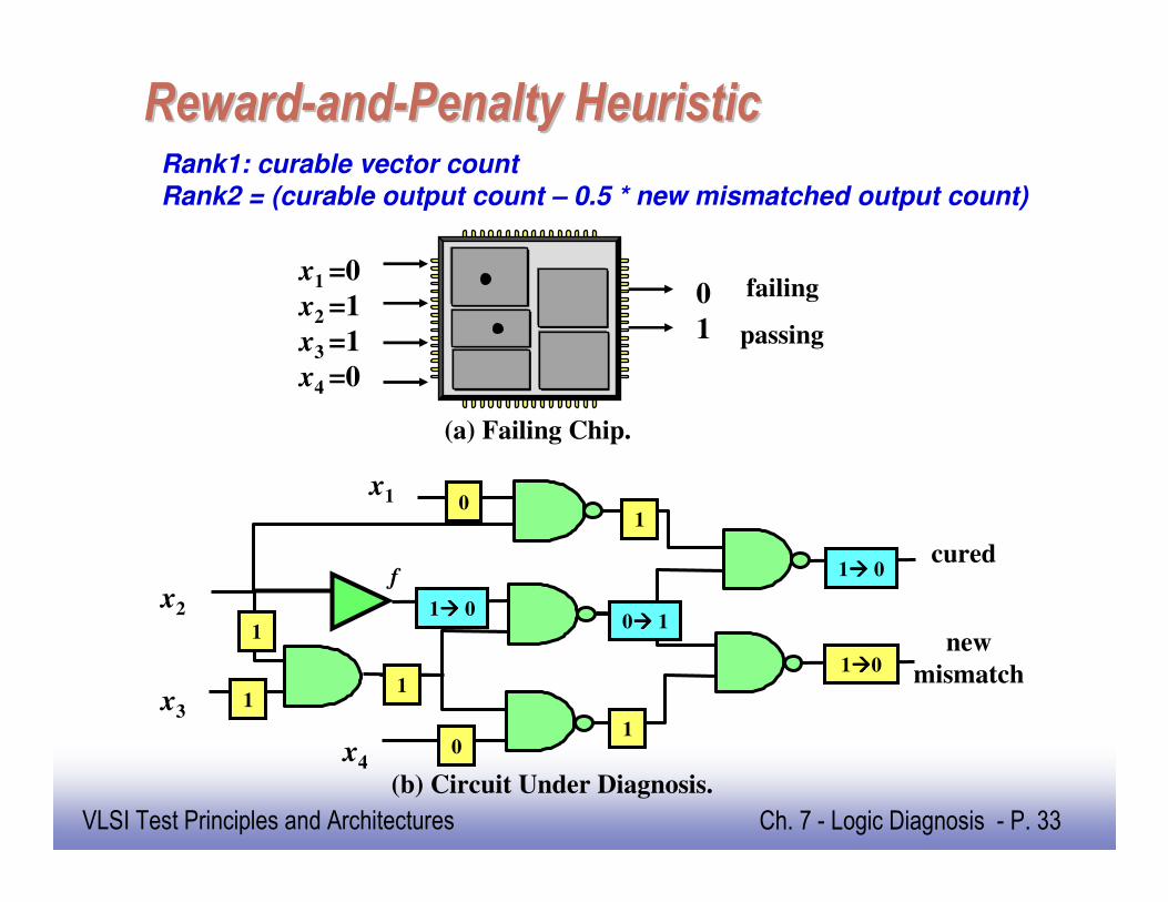
RewardReward--andand--Penalty HeuristicPenalty HeuristicRank1: curable vector count
Rank2 = (curable output count – 0.5 * new mismatched output count)
1
1
1
f
1���� 0
01
0���� 1
01
1���� 0
x1
x2
x3
x4
cured
0
1
x1 =0
x2 =1
x3 =1
x4 =0
(a) Failing Chip.
(b) Circuit Under Diagnosis.
1����0
failing
new
mismatch
passing

EE141
34
VLSI Test Principles and Architectures Ch. 7 - Logic Diagnosis - P. 34
Targeting Bridging FaultsTargeting Bridging Faults
w1
w2
A
B
C
D
bridging
Even in a realistic bridging fault, there is only one victim at any time.This victim will expose his location by owning some curable vectors.
EE141
35
VLSI Test Principles and Architectures Ch. 7 - Logic Diagnosis - P. 35
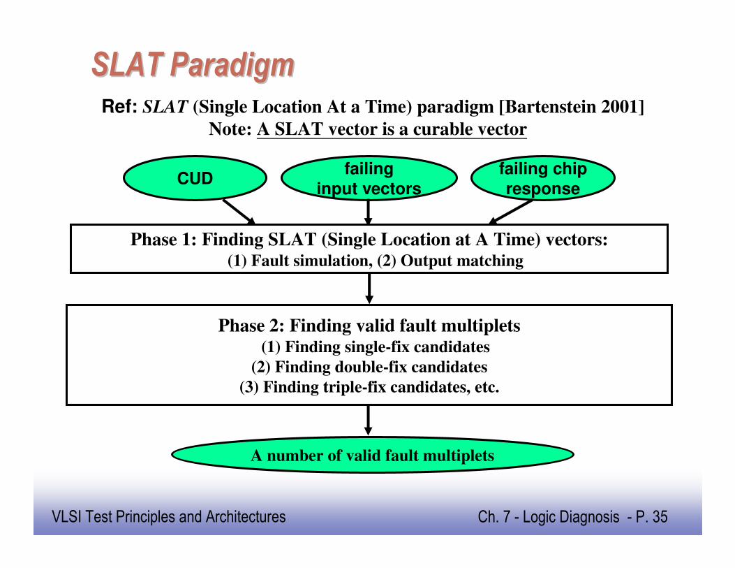
SLAT ParadigmSLAT Paradigm
A number of valid fault multiplets
CUDfailing
input vectorsfailing chipresponse
Phase 1: Finding SLAT (Single Location at A Time) vectors:(1) Fault simulation, (2) Output matching
Phase 2: Finding valid fault multiplets(1) Finding single-fix candidates
(2) Finding double-fix candidates
(3) Finding triple-fix candidates, etc.
Ref: SLAT (Single Location At a Time) paradigm [Bartenstein 2001]
Note: A SLAT vector is a curable vector
EE141
36
VLSI Test Principles and Architectures Ch. 7 - Logic Diagnosis - P. 36
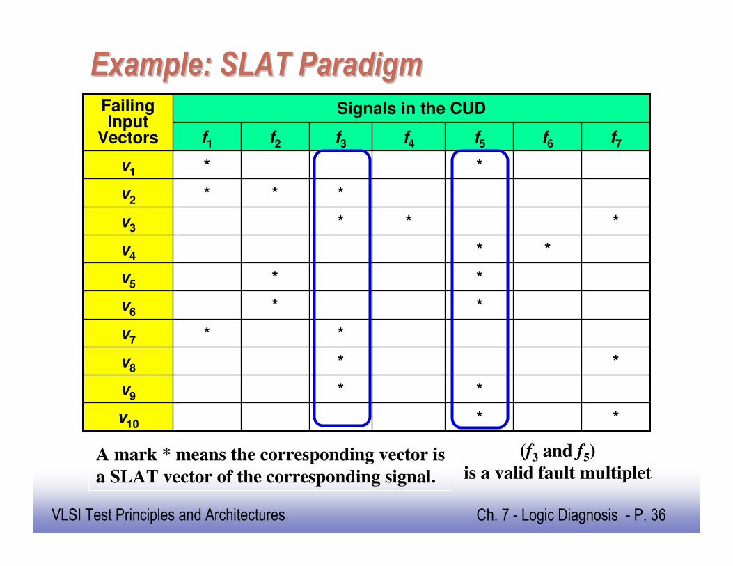
Example: SLAT ParadigmExample: SLAT ParadigmSignals in the CUD
**v9
**v4
**v5
**v6
**v7
**v8
f6
*
f4
*
*
f5
***v2
**v3
*v10
*v1
f7f3f2f1
FailingInput
Vectors
A mark * means the corresponding vector is
a SLAT vector of the corresponding signal.
(f3 and f5)
is a valid fault multiplet
EE141
37
VLSI Test Principles and Architectures Ch. 7 - Logic Diagnosis - P. 37
OutlineOutline
� Introduction
� Combinational Logic Diagnosis� Cause-Effect Analysis
� Effect-Cause Analysis
� Chip-Level Strategy
� Diagnostic Test Pattern Generation
� Scan Chain Diagnosis
� Logic BIST Diagnosis
� Conclusion
EE141
38
VLSI Test Principles and Architectures Ch. 7 - Logic Diagnosis - P. 38
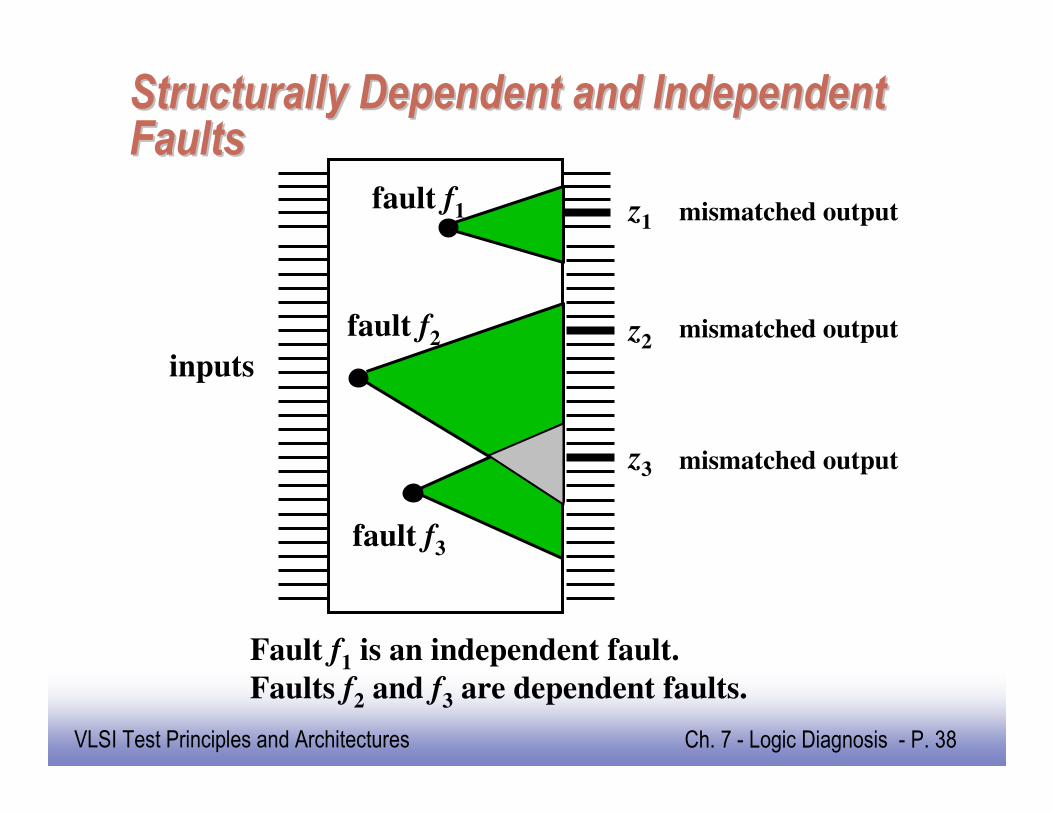
Structurally Dependent and Independent Structurally Dependent and Independent FaultsFaults
inputs
z1
z2
z3
fault f2
fault f1
fault f3
Fault f1 is an independent fault.
Faults f2 and f3 are dependent faults.
mismatched output
mismatched output
mismatched output

EE141
39
VLSI Test Principles and Architectures Ch. 7 - Logic Diagnosis - P. 39
Dependency GraphDependency Graph
z1
z2 z3
one connected component
z1
z2
z3fault
f2
fault f1
Two independent faults, f1 and f2, lead to one diagnosis block.
dependency graph
Direct divide-and-Conquerdoes not work well !
EE141
40
VLSI Test Principles and Architectures Ch. 7 - Logic Diagnosis - P. 40
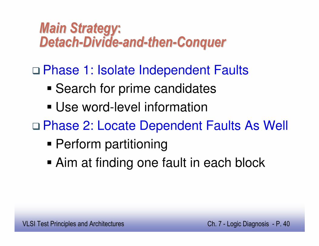
Main StrategyMain Strategy::
DetachDetach--DivideDivide--andand--thenthen--ConquerConquer
� Phase 1: Isolate Independent Faults
� Search for prime candidates
� Use word-level information
� Phase 2: Locate Dependent Faults As Well
� Perform partitioning
� Aim at finding one fault in each block
EE141
41
VLSI Test Principles and Architectures Ch. 7 - Logic Diagnosis - P. 41
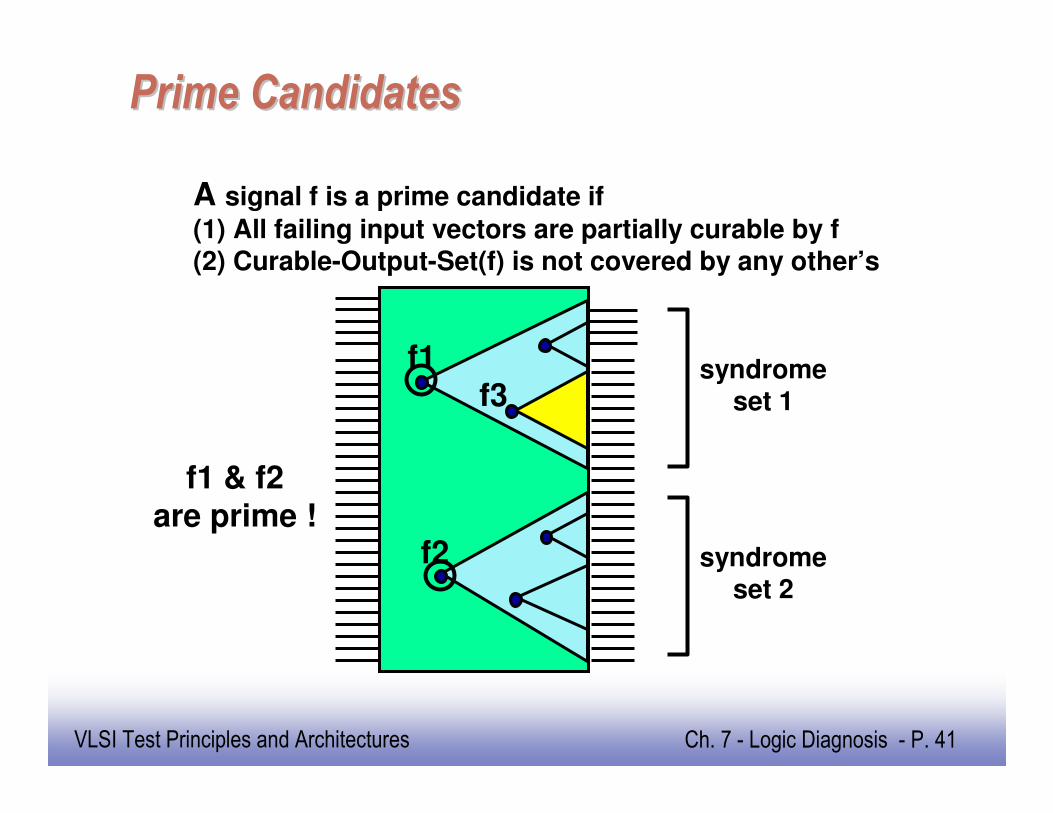
Prime CandidatesPrime Candidates
A signal f is a prime candidate if
(1) All failing input vectors are partially curable by f(2) Curable-Output-Set(f) is not covered by any other’s
f1
f2
f3
f1 & f2are prime !
syndromeset 1
syndromeset 2

EE141
42
VLSI Test Principles and Architectures Ch. 7 - Logic Diagnosis - P. 42
Fake Prime CandidatesFake Prime Candidates
� Structurally Independent Faults
� are often prime candidates
� Fake Prime Candidates
� are prime candidates that are NOT really faults - aliasing
f1
f2
f3
f4
f5
Example: Dependent Double Faults f1 & f2
May create fake prime candidates {f1, f2, f3}.
EE141
43
VLSI Test Principles and Architectures Ch. 7 - Logic Diagnosis - P. 43
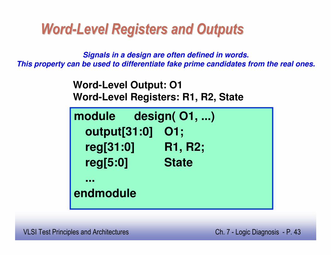
WordWord--Level Registers and OutputsLevel Registers and Outputs
module design( O1, ...)
output[31:0] O1;
reg[31:0] R1, R2;
reg[5:0] State
...
endmodule
Word-Level Output: O1Word-Level Registers: R1, R2, State
Signals in a design are often defined in words.This property can be used to differentiate fake prime candidates from the real ones.

EE141
44
VLSI Test Principles and Architectures Ch. 7 - Logic Diagnosis - P. 44
WordWord--Level Prime CandidatesLevel Prime Candidates
f1
f2
f3
f4
f5
f1
f2
f3
R
Z
R
Z
Note: Z and R are two word-level output groups.
Original prime candidates: {f1, f2}
Word-level prime candidates {f1, f2}
Assumed original prime candidates: {f3, f4 , f5}
{f4 , f5} will be identified as fake
���� Final Word-level prime candidates {f3}
EE141
45
VLSI Test Principles and Architectures Ch. 7 - Logic Diagnosis - P. 45
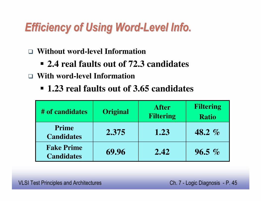
Efficiency of Using WordEfficiency of Using Word--Level Info.Level Info.
� Without word-level Information
� 2.4 real faults out of 72.3 candidates
� With word-level Information
� 1.23 real faults out of 3.65 candidates
96.5 %2.4269.96Fake Prime
Candidates
48.2 %1.232.375Prime
Candidates
Filtering
Ratio
After
FilteringOriginal# of candidates
EE141
46
VLSI Test Principles and Architectures Ch. 7 - Logic Diagnosis - P. 46
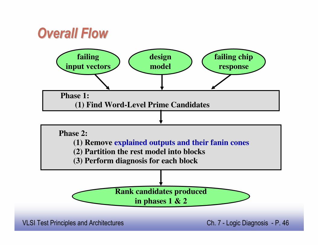
Overall FlowOverall Flow
Phase 1: (1) Find Word-Level Prime Candidates
Phase 2:
(1) Remove explained outputs and their fanin cones(2) Partition the rest model into blocks
(3) Perform diagnosis for each block
Rank candidates produced
in phases 1 & 2
failing
input vectors
design
model
failing chip
response
EE141
47
VLSI Test Principles and Architectures Ch. 7 - Logic Diagnosis - P. 47
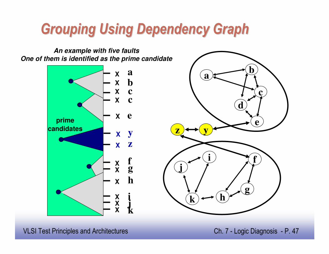
Grouping Using Dependency GraphGrouping Using Dependency Graph
X
X
X
X
X
XX
X
XX
X
abc
e
fg
ijk
c
h
i
h
f
g
j
k
ab
c
d
e
X
X
yz
yzprime
candidates
An example with five faultsOne of them is identified as the prime candidate
EE141
48
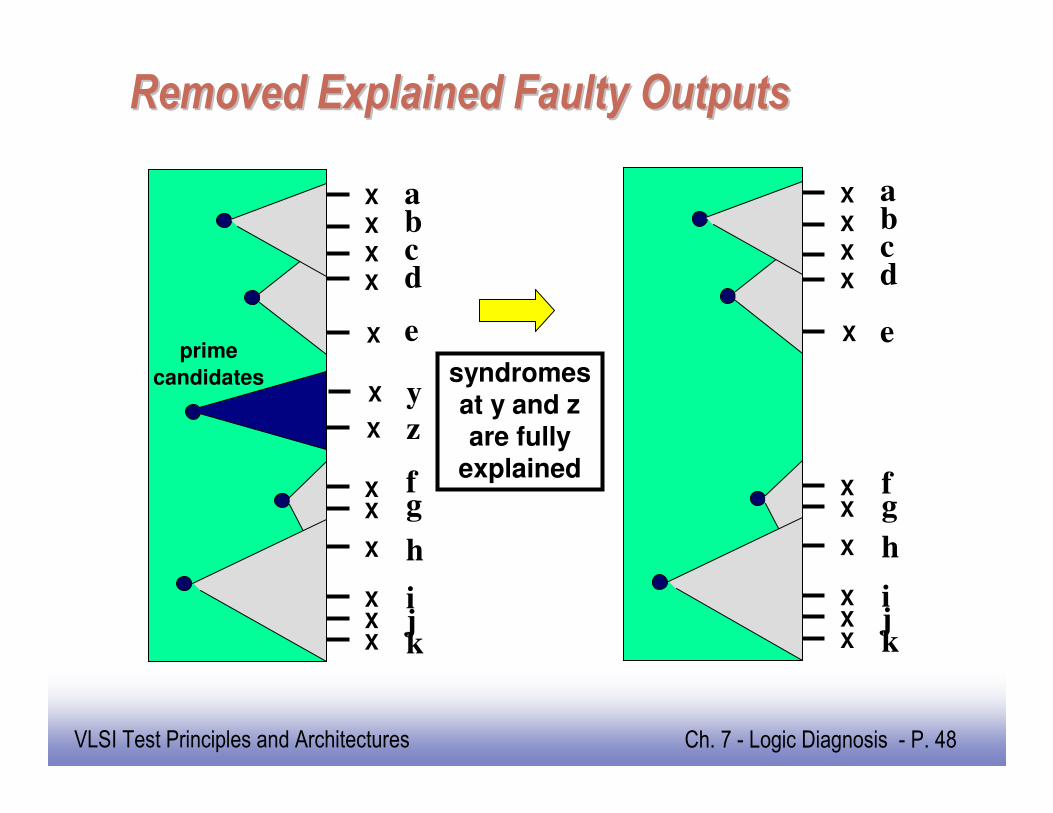
VLSI Test Principles and Architectures Ch. 7 - Logic Diagnosis - P. 48
Removed Explained Faulty OutputsRemoved Explained Faulty Outputs
X
X
X
X
X
XX
X
XX
X
abc
e
fg
ijk
d
h
X
X
y
z
prime
candidates
X
X
X
X
X
XX
X
XX
X
abc
e
fg
ijk
d
h
syndromesat y and zare fully
explained
EE141
49
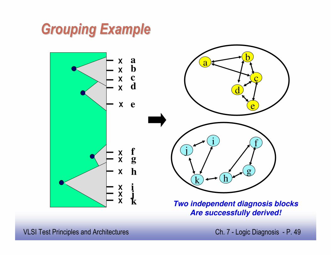
VLSI Test Principles and Architectures Ch. 7 - Logic Diagnosis - P. 49
Grouping ExampleGrouping Example
i
h
f
g
j
k
ab
c
d
e
X
X
X
X
X
XX
X
XX
X
abc
e
fg
ijk
d
h
Two independent diagnosis blocksAre successfully derived!
EE141
50
VLSI Test Principles and Architectures Ch. 7 - Logic Diagnosis - P. 50
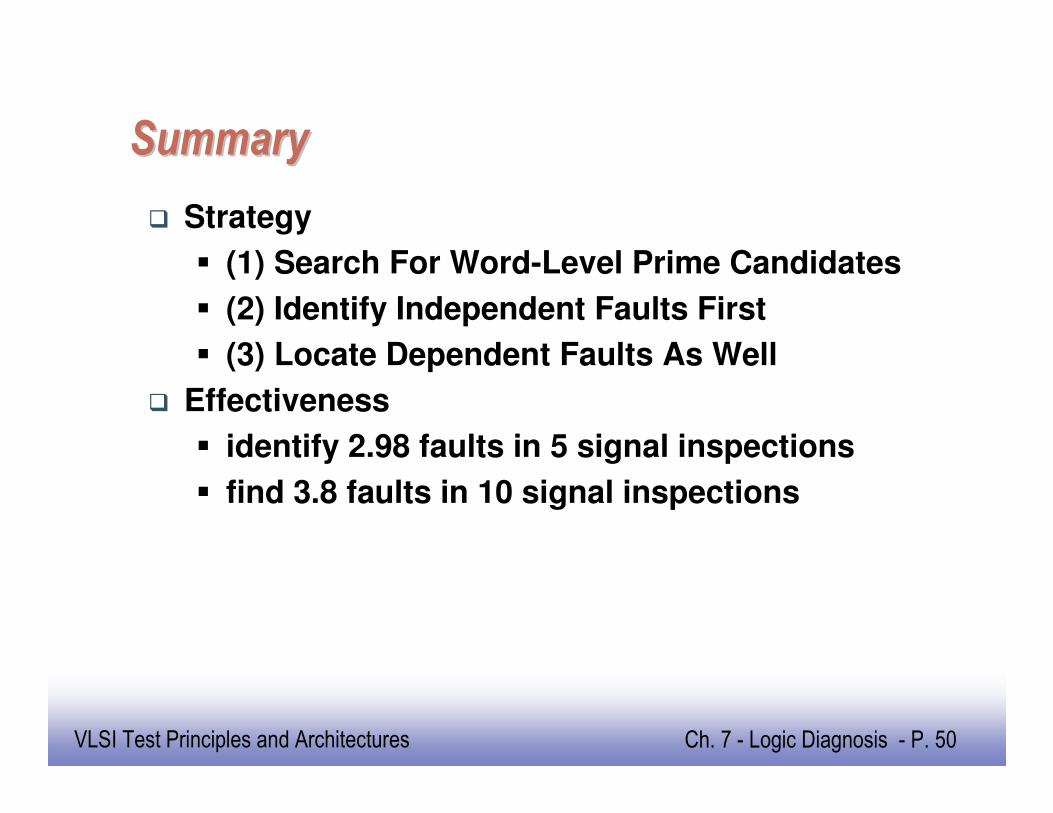
SummarySummary
� Strategy
� (1) Search For Word-Level Prime Candidates
� (2) Identify Independent Faults First
� (3) Locate Dependent Faults As Well
� Effectiveness
� identify 2.98 faults in 5 signal inspections
� find 3.8 faults in 10 signal inspections
EE141
51
VLSI Test Principles and Architectures Ch. 7 - Logic Diagnosis - P. 51
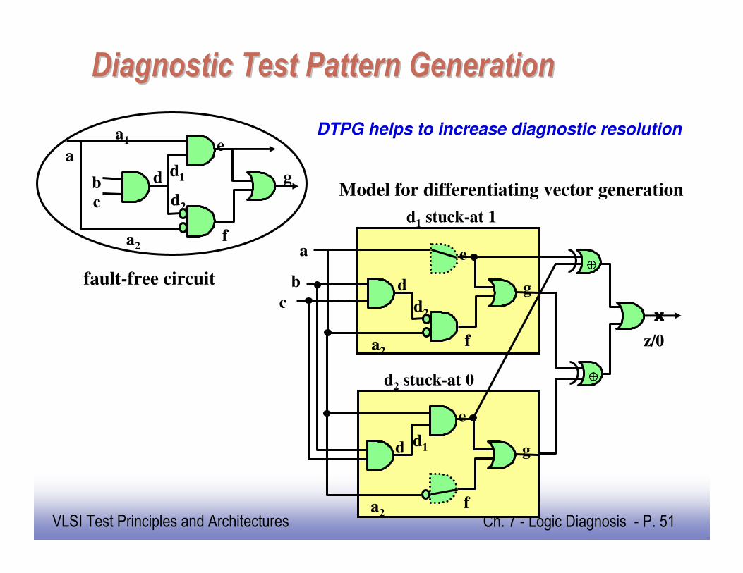
Diagnostic Test Pattern GenerationDiagnostic Test Pattern Generation
fault-free circuit
c
b
a e
d
a2
d2
f
g
d1 stuck-at 1
e
d
a2
d1
f
g
xxxx
d2 stuck-at 0
a
b
c
e
d
a1
a2
d1
d2
f
g
⊕⊕⊕⊕
⊕⊕⊕⊕
z/0
Model for differentiating vector generation
DTPG helps to increase diagnostic resolution
EE141
52
VLSI Test Principles and Architectures Ch. 7 - Logic Diagnosis - P. 52
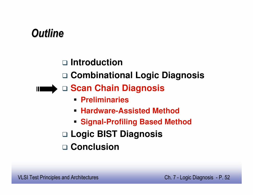
OutlineOutline
� Introduction
� Combinational Logic Diagnosis
� Scan Chain Diagnosis
� Preliminaries
� Hardware-Assisted Method
� Signal-Profiling Based Method
� Logic BIST Diagnosis
� Conclusion
EE141
53
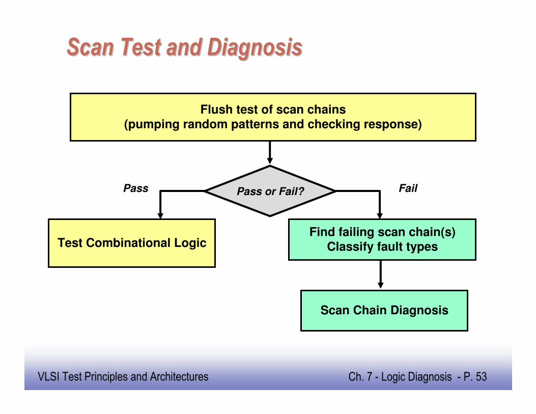
VLSI Test Principles and Architectures Ch. 7 - Logic Diagnosis - P. 53
Scan Test and DiagnosisScan Test and Diagnosis
Flush test of scan chains(pumping random patterns and checking response)
Pass or Fail?
Test Combinational Logic
Pass Fail
Scan Chain Diagnosis
Find failing scan chain(s)Classify fault types
EE141
54
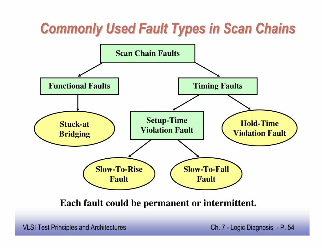
VLSI Test Principles and Architectures Ch. 7 - Logic Diagnosis - P. 54
Commonly Used Fault Types in Scan ChainsCommonly Used Fault Types in Scan Chains
Each fault could be permanent or intermittent.
Scan Chain Faults
Functional Faults Timing Faults
Setup-Time
Violation FaultStuck-at
Bridging
Slow-To-Rise
Fault
Slow-To-Fall
Fault
Hold-Time
Violation Fault
EE141
55
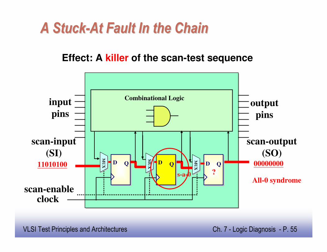
VLSI Test Principles and Architectures Ch. 7 - Logic Diagnosis - P. 55
A StuckA Stuck--At Fault In the ChainAt Fault In the Chain
Effect: A killer of the scan-test sequence
D Q
input
pins
clock
output
pins
D Q D Q
Combinational Logic
scan-input
(SI)
scan-output
(SO)
MU
X
MU
X
MU
X
scan-enable
11010100 00000000
s-a-0 ?All-0 syndrome
EE141
56
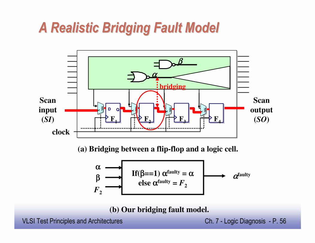
VLSI Test Principles and Architectures Ch. 7 - Logic Diagnosis - P. 56
A Realistic Bridging Fault ModelA Realistic Bridging Fault Model
clock
Scan
input
(SI)
Scan
output
(SO)
D Q
MUX
MUX
MUX
MUX
F1 F2 F3 F4
αααα
ββββ
bridging
(a) Bridging between a flip-flop and a logic cell.
(b) Our bridging fault model.
If(ββββ==1) ααααfaulty = ααααelse ααααfaulty = F2
ααααfaulty
αααα
ββββ
F2
EE141
57
VLSI Test Principles and Architectures Ch. 7 - Logic Diagnosis - P. 57
Potential HoldPotential Hold--Time Fault?Time Fault?
(Negative Edge-Triggered Flip-Flop)
CLK = high
Master Slave
D QY
CLK = low
Master Slave
D QY
CLK = low
Master Slave
D QY
faulty
normal
shut downtoo slowly
EE141
58
VLSI Test Principles and Architectures Ch. 7 - Logic Diagnosis - P. 58
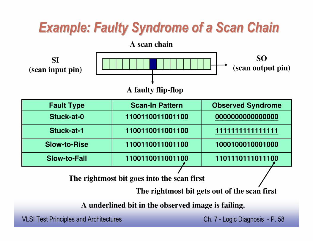
Example: Faulty Syndrome of a Scan ChainExample: Faulty Syndrome of a Scan Chain
11011101110111001100110011001100Slow-to-Fall
10001000100010001100110011001100Slow-to-Rise
11111111111111111100110011001100Stuck-at-1
00000000000000001100110011001100Stuck-at-0
Observed SyndromeScan-In PatternFault Type
SI
(scan input pin)
SO
(scan output pin)
A faulty flip-flop
A scan chain
A underlined bit in the observed image is failing.
The rightmost bit goes into the scan first
The rightmost bit gets out of the scan first
EE141
59
VLSI Test Principles and Architectures Ch. 7 - Logic Diagnosis - P. 59
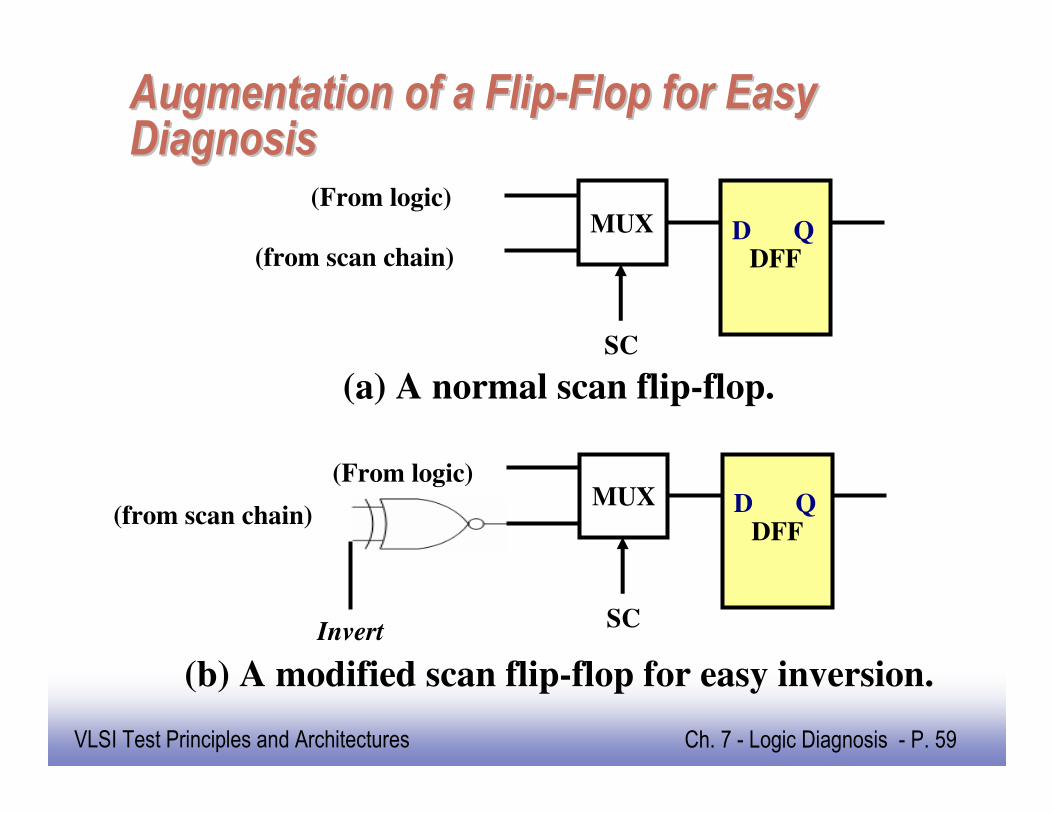
Augmentation of a FlipAugmentation of a Flip--Flop for Easy Flop for Easy DiagnosisDiagnosis
DFF
MUX(From logic)
(from scan chain)QD
SC
DFF
MUX(From logic)
(from scan chain) QD
SCInvert
(a) A normal scan flip-flop.
(b) A modified scan flip-flop for easy inversion.
EE141
60
VLSI Test Principles and Architectures Ch. 7 - Logic Diagnosis - P. 60
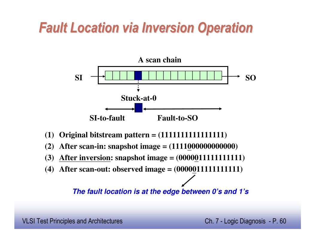
Fault Location via Inversion OperationFault Location via Inversion Operation
SI SO
Stuck-at-0
A scan chain
(1) Original bitstream pattern = (1111111111111111)
(2) After scan-in: snapshot image = (1111000000000000)
(3) After inversion: snapshot image = (0000011111111111)
(4) After scan-out: observed image = (0000011111111111)
Fault-to-SOSI-to-fault
The fault location is at the edge between 0’s and 1’s
EE141
61
VLSI Test Principles and Architectures Ch. 7 - Logic Diagnosis - P. 61
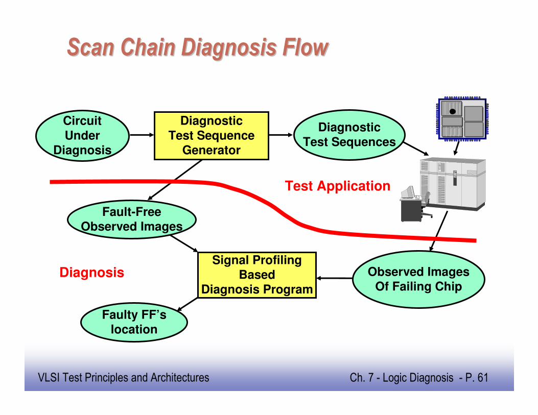
Scan Chain Diagnosis FlowScan Chain Diagnosis Flow
Circuit
UnderDiagnosis
Diagnostic
Test SequenceGenerator
DiagnosticTest Sequences
Fault-FreeObserved Images
Signal ProfilingBased
Diagnosis Program
Faulty FF’slocation
Observed ImagesOf Failing Chip
Diagnosis
Test Application

EE141
62
VLSI Test Principles and Architectures Ch. 7 - Logic Diagnosis - P. 62
Definition: Snapshot ImageDefinition: Snapshot Image
input
pins
clock
output
pins
Scan
input
(SI)
Scan
output
(SO)
Mission Logic
00000000D Q
11111111 00000000
MU
X
MU
X
MU
X
xs-a-0 11111111
MU
X
Snapshot image: {(F1, F2, F3, F4) | (0, 1, 0, 1)}
F1 F2 F3 F4
Def: A snapshot image is the combination of flip-flop values
at certain time instance
EE141
63
VLSI Test Principles and Architectures Ch. 7 - Logic Diagnosis - P. 63
Definition: Observed ImageDefinition: Observed Image
Def: An observed image is the scanned-out version of
a snapshot image.
input
pins
clock
output
pins
Scan
input
(SI)
Scan
output
(SO)
Mission Logic
00000000D Q
11111111 00000000
MU
X
MU
X
MU
Xxs-a-0 11111111
MU
X
Snapshot image: {(F1, F2, F3, F4) | (0, 1, 0, 1)}
Observed image: {(F1, F2, F3, F4) | (0, 0, 0, 1)}
F1 F2 F3 F4
EE141
64
VLSI Test Principles and Architectures Ch. 7 - Logic Diagnosis - P. 64
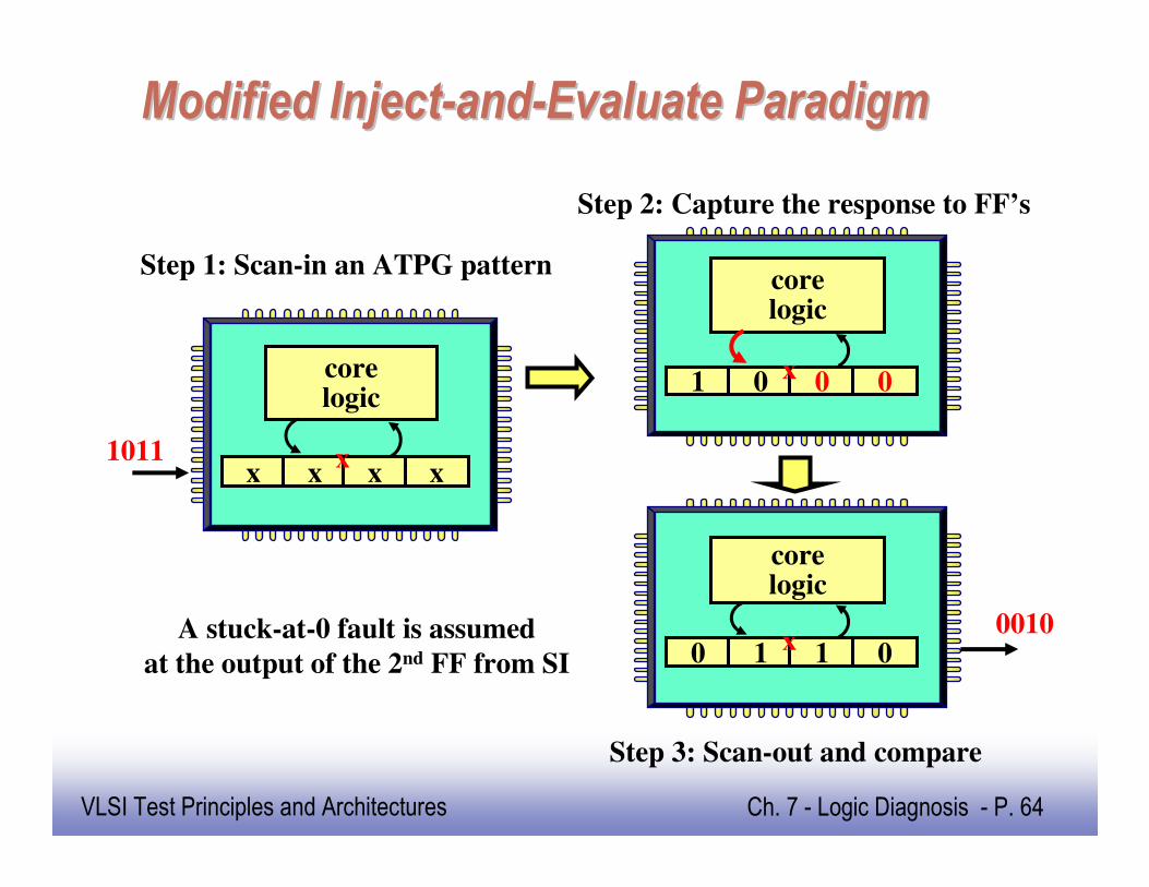
Modified InjectModified Inject--andand--Evaluate ParadigmEvaluate Paradigm
x x x x
corelogic
x1011
Step 1: Scan-in an ATPG pattern
1 0 0 0
corelogic
x
0 1 1 0
corelogic
x0010
Step 2: Capture the response to FF’s
Step 3: Scan-out and compare
A stuck-at-0 fault is assumed
at the output of the 2nd FF from SI
EE141
65
VLSI Test Principles and Architectures Ch. 7 - Logic Diagnosis - P. 65
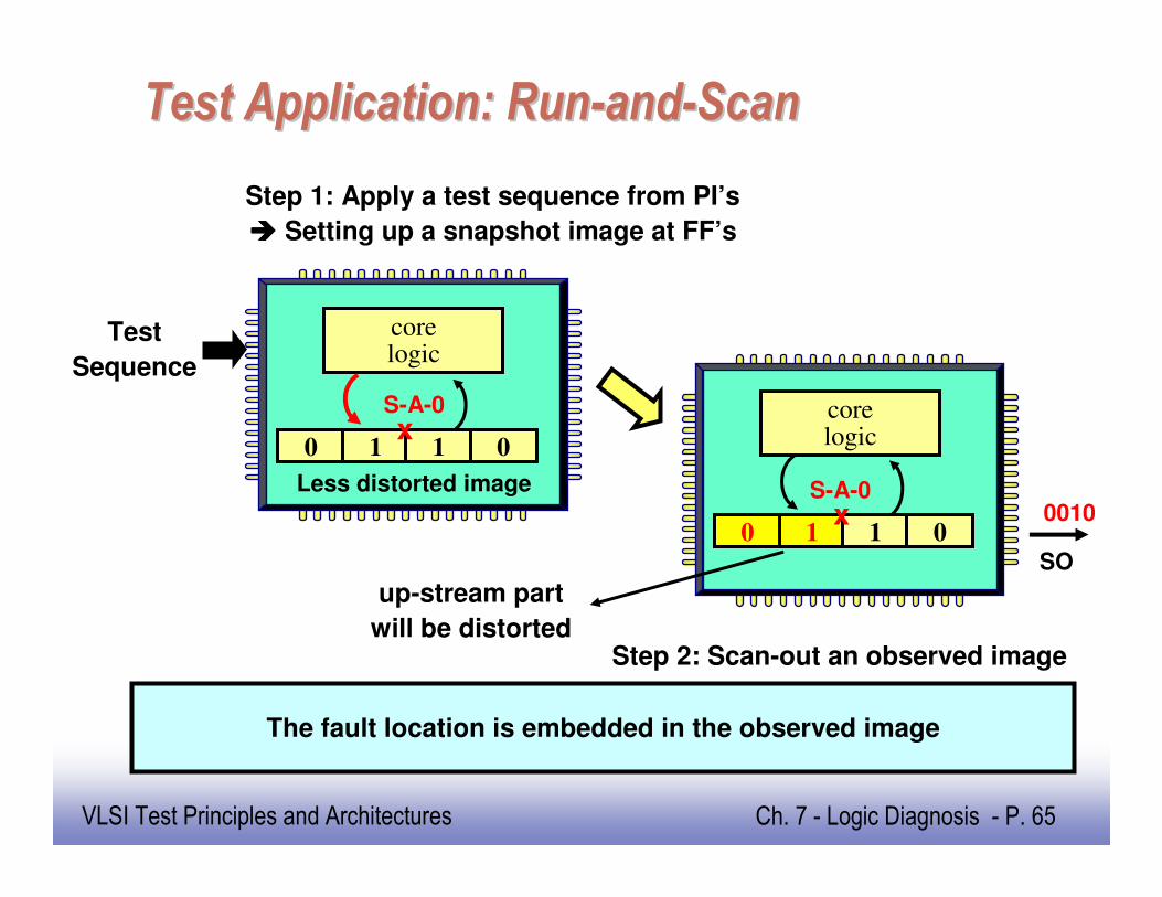
Test Application: RunTest Application: Run--andand--ScanScan
Step 1: Apply a test sequence from PI’s
���� Setting up a snapshot image at FF’s
Step 2: Scan-out an observed image
0 1 1 0
corelogic
xS-A-0
0 1 1 0
corelogic
x 0010
SO
S-A-0
up-stream part
will be distorted
Less distorted image
Test
Sequence
The fault location is embedded in the observed image
EE141
66
VLSI Test Principles and Architectures Ch. 7 - Logic Diagnosis - P. 66
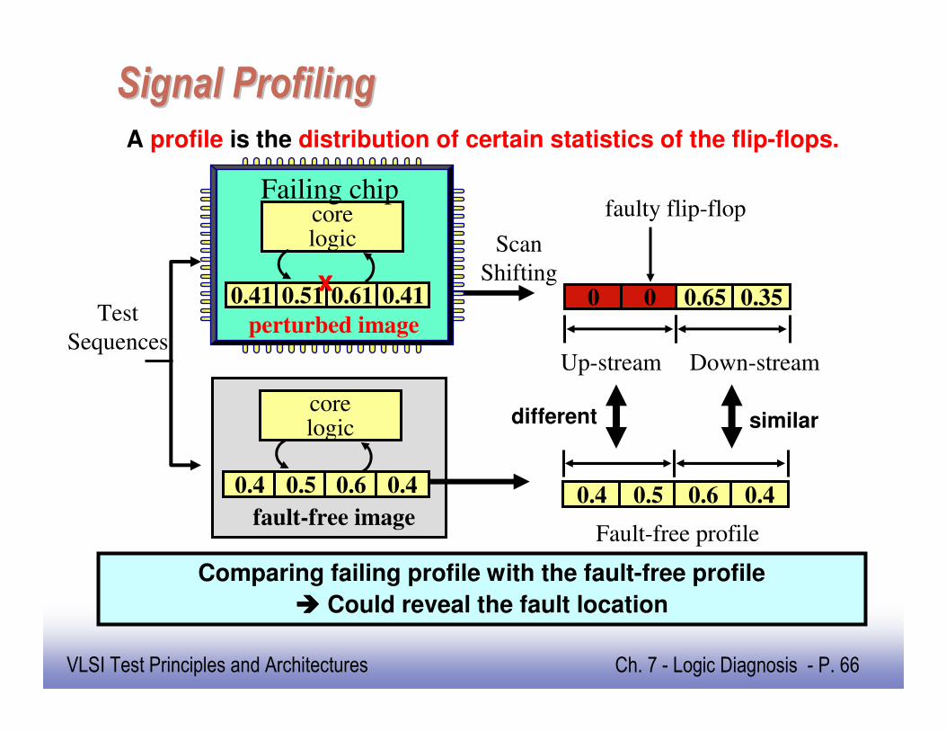
Signal ProfilingSignal ProfilingA profile is the distribution of certain statistics of the flip-flops.
Fault-free model
faulty flip-flop
Up-stream Down-stream
0 0 0.65 0.35
0.4 0.5 0.6 0.4
corelogic
Test
Sequences
fault-free image
Scan
Shifting0.41 0.51 0.61 0.41
corelogic
perturbed image
Failing chip
x
0.4 0.5 0.6 0.4
similardifferent
Fault-free profile
Comparing failing profile with the fault-free profile
���� Could reveal the fault location
EE141
67
VLSI Test Principles and Architectures Ch. 7 - Logic Diagnosis - P. 67
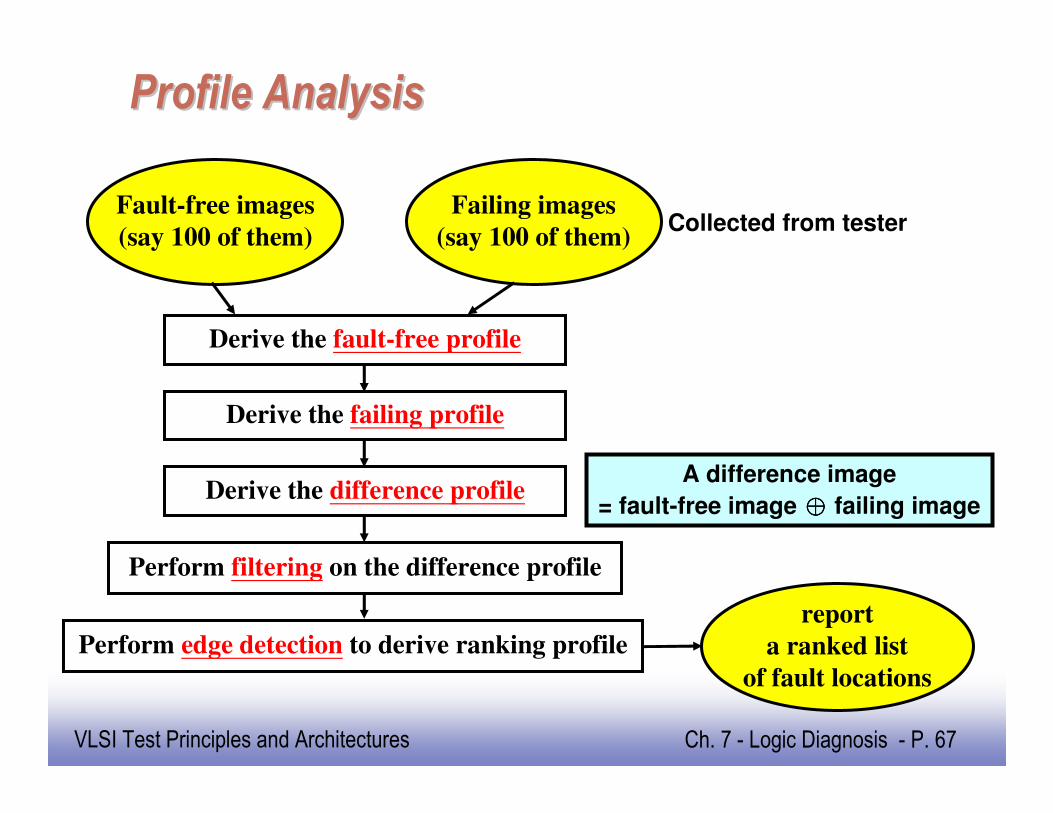
Profile AnalysisProfile Analysis
Fault-free images
(say 100 of them)
Failing images
(say 100 of them)
report
a ranked list
of fault locations
Derive the fault-free profile
Derive the failing profile
Derive the difference profile
Perform filtering on the difference profile
Perform edge detection to derive ranking profile
A difference image
= fault-free image ⊕⊕⊕⊕ failing image
Collected from tester
EE141
68
VLSI Test Principles and Architectures Ch. 7 - Logic Diagnosis - P. 68
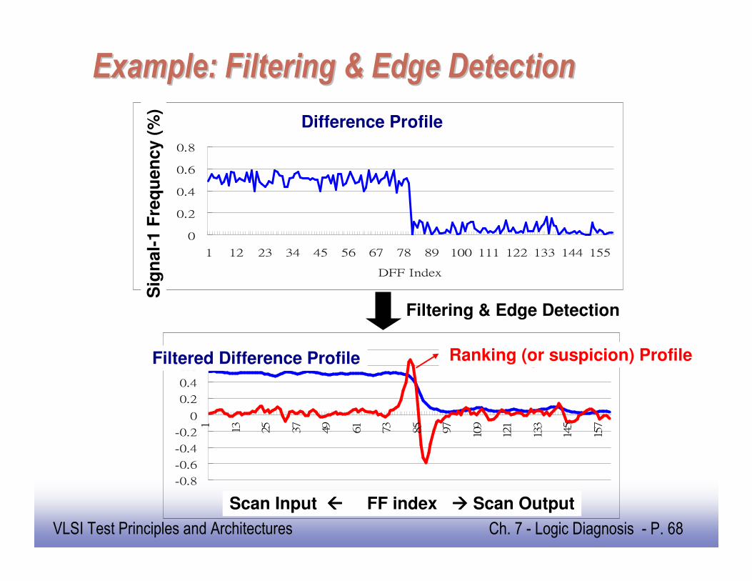
Example: Filtering & Edge DetectionExample: Filtering & Edge Detection
Profiling difference
0
0.2
0.4
0.6
0.8
1 12 23 34 45 56 67 78 89 100 111 122 133 144 155
DFF Index
SP (%
)S
ign
al-
1 F
req
uen
cy (
%)
Difference Profile
-0.8
-0.6
-0.4
-0.2
0
0.2
0.4
0.6
0.8
1 13 25 37 49 61 73 85 97 109
121
133
145
157
DFF Index
Smooth Profile Ranking ProfileRanking (or suspicion) ProfileFiltered Difference Profile
Filtering & Edge Detection
Scan Input FF index ���� Scan Output

EE141
69
VLSI Test Principles and Architectures Ch. 7 - Logic Diagnosis - P. 69
Computation of AverageComputation of Average--Sum FilteringSum Filtering
� (Average-sum filtering) Assume that the difference
profile is given and denoted as D[i], where i is the index
of a flip-flop. We use the following formula to compute
a smoothed difference profile, SD[i]:
SD[i] = 0.2*(D[i-2]+ D[i-1]+ D[i]+ D[i+1]+ D[i+2])
EE141
70
VLSI Test Principles and Architectures Ch. 7 - Logic Diagnosis - P. 70
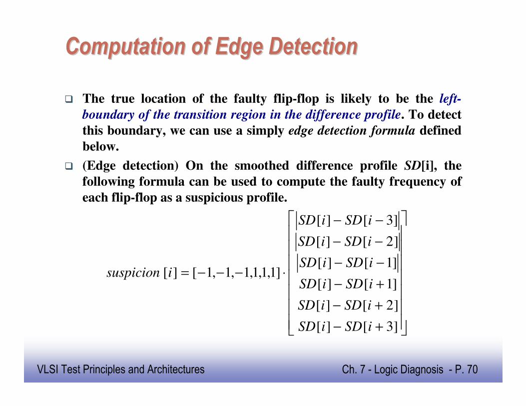
Computation of Edge DetectionComputation of Edge Detection
� The true location of the faulty flip-flop is likely to be the left-
boundary of the transition region in the difference profile. To detect
this boundary, we can use a simply edge detection formula defined
below.
� (Edge detection) On the smoothed difference profile SD[i], the
following formula can be used to compute the faulty frequency of
each flip-flop as a suspicious profile.
+−
+−
+−
−−
−−
−−
⋅−−−=
]3[][
]2[][
]1[][
]1[][
]2[][
]3[][
]1,1,1,1,1,1[][
iSDiSD
iSDiSD
iSDiSD
iSDiSD
iSDiSD
iSDiSD
isuspicion
EE141
71
VLSI Test Principles and Architectures Ch. 7 - Logic Diagnosis - P. 71
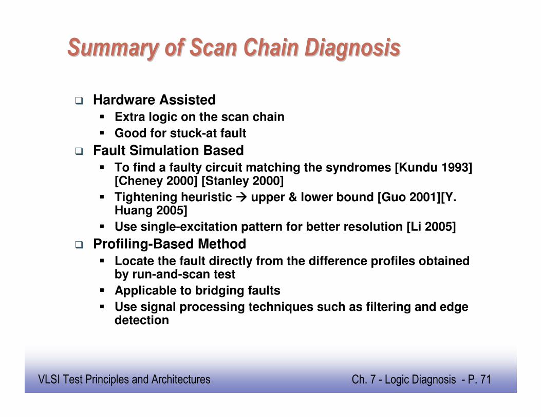
Summary of Scan Chain DiagnosisSummary of Scan Chain Diagnosis
� Hardware Assisted
� Extra logic on the scan chain
� Good for stuck-at fault
� Fault Simulation Based
� To find a faulty circuit matching the syndromes [Kundu 1993] [Cheney 2000] [Stanley 2000]
� Tightening heuristic ���� upper & lower bound [Guo 2001][Y. Huang 2005]
� Use single-excitation pattern for better resolution [Li 2005]
� Profiling-Based Method
� Locate the fault directly from the difference profiles obtained by run-and-scan test
� Applicable to bridging faults
� Use signal processing techniques such as filtering and edge detection
EE141
72
VLSI Test Principles and Architectures Ch. 7 - Logic Diagnosis - P. 72
OutlineOutline
� Introduction
� Combinational Logic Diagnosis
� Scan Chain Diagnosis
� Logic BIST Diagnosis
� Overview
� Interval-Based Method
� Masking-Based Method
� Conclusion
EE141
73
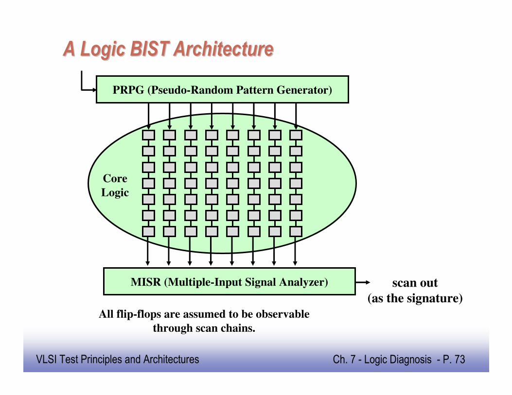
VLSI Test Principles and Architectures Ch. 7 - Logic Diagnosis - P. 73
A Logic BIST ArchitectureA Logic BIST Architecture
MISR (Multiple-Input Signal Analyzer)
Core
Logic
All flip-flops are assumed to be observable
through scan chains.
scan out
(as the signature)
PRPG (Pseudo-Random Pattern Generator)
EE141
74
VLSI Test Principles and Architectures Ch. 7 - Logic Diagnosis - P. 74
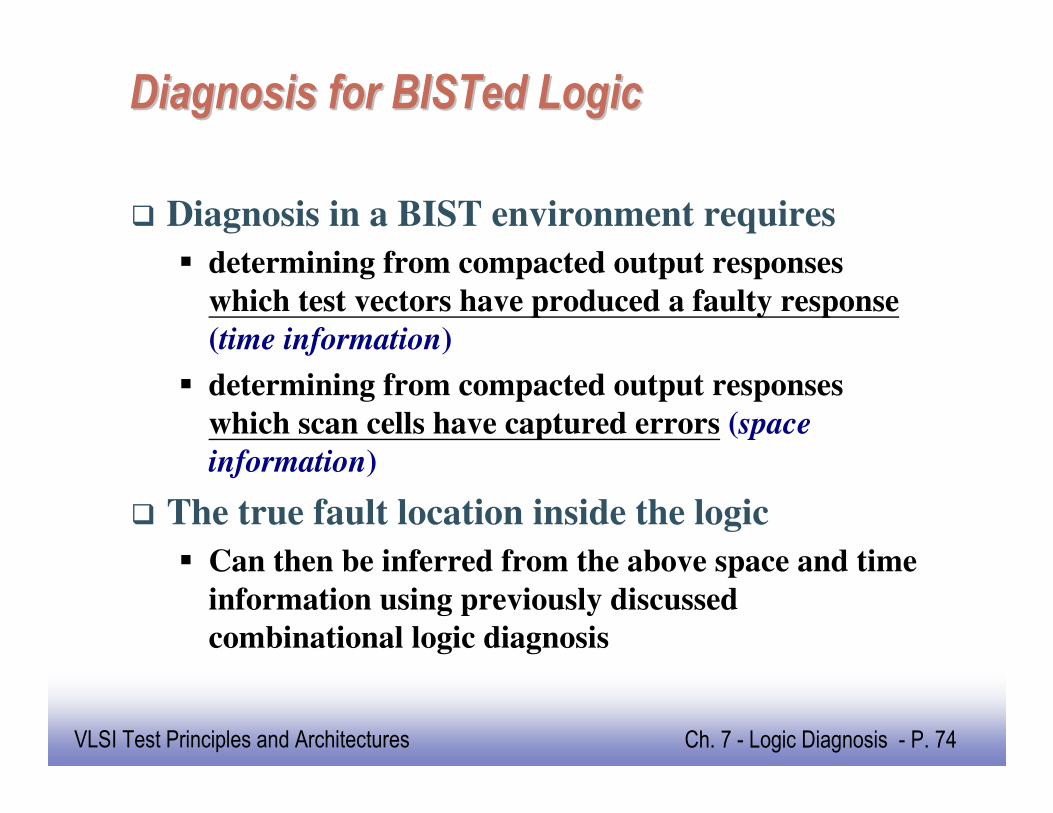
Diagnosis for Diagnosis for BISTedBISTed LogicLogic
� Diagnosis in a BIST environment requires
� determining from compacted output responses
which test vectors have produced a faulty response
(time information)
� determining from compacted output responses
which scan cells have captured errors (space
information)
� The true fault location inside the logic
� Can then be inferred from the above space and time
information using previously discussed
combinational logic diagnosis
EE141
75
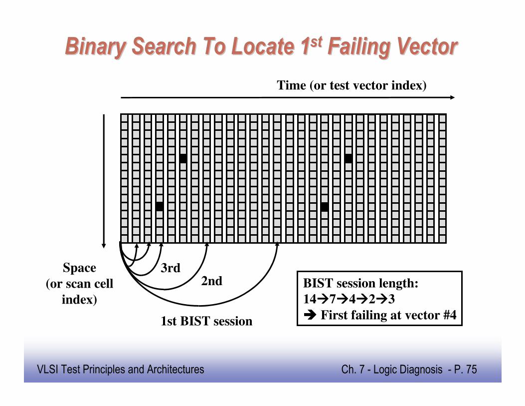
VLSI Test Principles and Architectures Ch. 7 - Logic Diagnosis - P. 75
Binary Search To Locate 1Binary Search To Locate 1stst Failing VectorFailing Vector
Time (or test vector index)
Space
(or scan cell
index)
1st BIST session
2nd3rd
BIST session length:
14����7����4����2����3
���� First failing at vector #4
EE141
76
VLSI Test Principles and Architectures Ch. 7 - Logic Diagnosis - P. 76
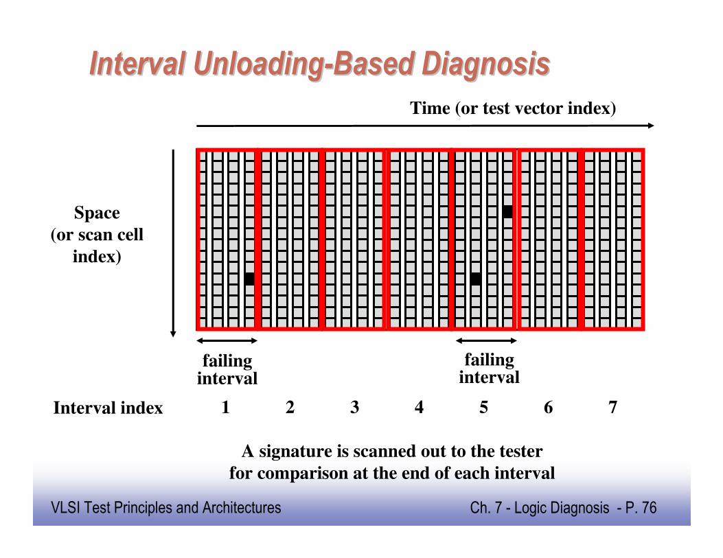
Interval UnloadingInterval Unloading--Based DiagnosisBased Diagnosis
Time (or test vector index)
Space
(or scan cell
index)
A signature is scanned out to the tester
for comparison at the end of each interval
failinginterval
Interval index 1 2 3 4 5 6 7
failinginterval
EE141
77
VLSI Test Principles and Architectures Ch. 7 - Logic Diagnosis - P. 77
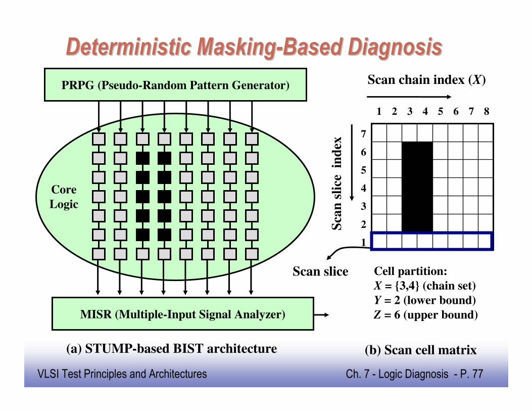
Deterministic MaskingDeterministic Masking--Based DiagnosisBased Diagnosis
MISR (Multiple-Input Signal Analyzer)
Core
Logic
PRPG (Pseudo-Random Pattern Generator)
(a) STUMP-based BIST architecture (b) Scan cell matrix
Scan chain index (X)
Sca
n s
lice
in
dex
7
6
5
4
3
2
1
Cell partition:
X = {3,4} (chain set)
Y = 2 (lower bound)
Z = 6 (upper bound)
Scan slice
1 2 3 4 5 6 7 8
EE141
78
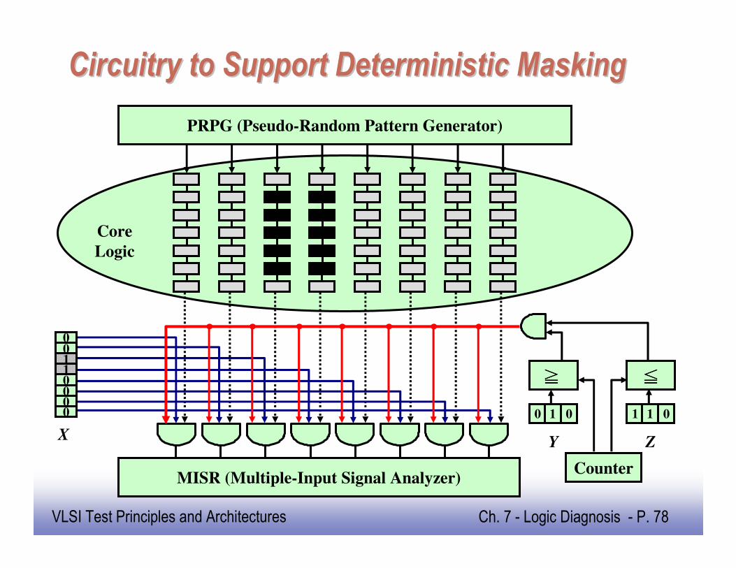
VLSI Test Principles and Architectures Ch. 7 - Logic Diagnosis - P. 78
Circuitry to Support Deterministic MaskingCircuitry to Support Deterministic Masking
MISR (Multiple-Input Signal Analyzer)
Core
Logic
PRPG (Pseudo-Random Pattern Generator)
00110000
X Y
0 1 0
Z
1 1 0
≧≧≧≧ ≦≦≦≦
Counter
EE141
79
VLSI Test Principles and Architectures Ch. 7 - Logic Diagnosis - P. 79
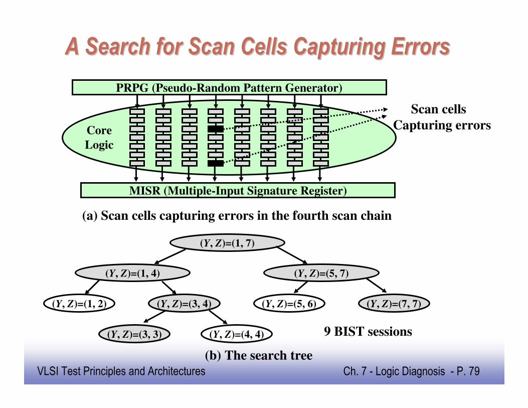
A Search for Scan Cells Capturing ErrorsA Search for Scan Cells Capturing Errors
MISR (Multiple-Input Signature Register)
Core
Logic
PRPG (Pseudo-Random Pattern Generator)
Scan cells
Capturing errors
(Y, Z)=(1, 7)
(Y, Z)=(1, 4) (Y, Z)=(5, 7)
(Y, Z)=(1, 2) (Y, Z)=(3, 4) (Y, Z)=(5, 6) (Y, Z)=(7, 7)
(Y, Z)=(3, 3) (Y, Z)=(4, 4) 9 BIST sessions
(b) The search tree
(a) Scan cells capturing errors in the fourth scan chain
EE141
80
VLSI Test Principles and Architectures Ch. 7 - Logic Diagnosis - P. 80
ConclusionsConclusions
� Logic diagnosis for combinational logic
� Has been mature
� Good for not just stuck-at faults, but also bridging faults
� Scan chain diagnosis
� Making good progress …
� Fault-simulation-based, or signal-profiling based
� Diagnosis of scan-based logic BIST
� Hardware support is often required
� Interval-unloading, or masking-based
� Future challenges
� Performance (speed) debug
� Diagnosis for logic with on-chip test compression and
decompression
� Diagnosis for parametric yield loss due to nanometer effects