channel control asic for the cms hadron calorimeter front end readout...
TRANSCRIPT

September 8-14, 2002 7th Workshop on Electronics for LHC 1
Channel Control ASIC for theCMS Hadron Calorimeter Front
End Readout Module
Ray Yarema, Alan Baumbaugh,Ahmed Boubekeur, John Elias,
Theresa ShawSeptember 12, 2002

September 8-14, 2002 7th Workshop on Electronics for LHC 2
CCA Use in CMS
• CCAs are used for processing both HPD and PMTsignals
• CCA provides control and interface for QIEASICs which digitize charge input signals.
• CCAs and QIEs are mounted on the CMS HadronCalorimeter Front End Readout Module
• CCAs and QIEs were designed at Fermilab

September 8-14, 2002 7th Workshop on Electronics for LHC 3
Front End Readout Module
• Two QIE chipsinterface to oneCCA chip
• There are 3CCA chips on aFront EndReadout Module
• 3 CCAs feeddata to 2 GOLs
QIECCA
QIE
QIE
QIE
QIE
QIE
CCA
CCA
Front End Readout ModuleFromHPD orPMT
VCSEL
VCSEL
GOL
GOL VCSEL

September 8-14, 2002 7th Workshop on Electronics for LHC 4
Hadron Calorimeter Front End Module

September 8-14, 2002 7th Workshop on Electronics for LHC 5
What is a QIE?(Charge Integrator and Encoder)
• QIE digitizes input signal overa wide dynamic range
• QIE operates in a 4 steppipeline mode
• The data is output as a 2 bitexponent and 5 bit mantissaalong with the time sliceinformation which is referred toas Cap ID
• QIE can be programmed toaccept either positive (PMT) ornegative (HPD) input charge
HPD Input
PMT InputQIE
Exponent
Mantissa
Cap ID
2
5
2
QIE Clock

September 8-14, 2002 7th Workshop on Electronics for LHC 6
Primary Functions of CCA
• Send individually programmable delayedclocks to each of the QIEs, to correct fortime differences within the hadroncalorimeter (58 nsec max)
• Accept exponent and mantissa informationfrom 2 QIEs, align the data and send thedata to a gigabit serializer that drives anoptical link

September 8-14, 2002 7th Workshop on Electronics for LHC 7
Other CCA Features• Provide RBX serial
interface, similar to I2C,for programming features
• See that QIEs areoperating in sync bychecking QIE capacitorIDs
• Force QIE into fixed rangeinstead of autoranging fortest purposes
• Adjust QIE pedestal levelto correct for HPD leakage
• Reset QIEs• Place QIE in calibration
mode• Issue test pulse triggers of
programmable polarity foreither HPD or PMT
• Flag zero crossing countercheck error
• Test pattern registers tocheck operation of DAQ
September 8-14, 2002 7th Workshop on Electronics for LHC 8
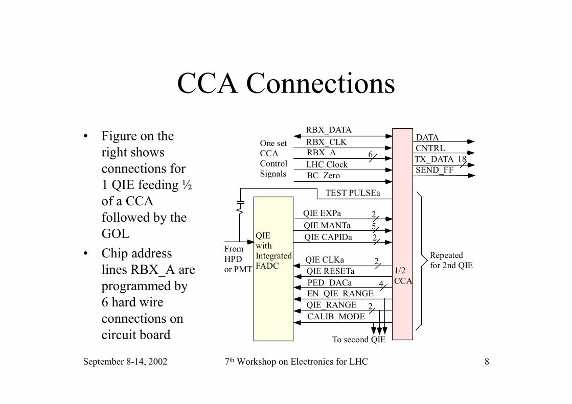
CCA Connections• Figure on the
right showsconnections for1 QIE feeding ½of a CCAfollowed by theGOL
• Chip addresslines RBX_A areprogrammed by6 hard wireconnections oncircuit board
QIE EXPaQIE MANTaQIE CAPIDa
QIE CLKaQIE RESETaPED_DACa
QIE_RANGECALIB_MODE
EN_QIE_RANGE
To second QIE
1/2CCA
QIEwithIntegratedFADC
FromHPDor PMT
TEST PULSEa
RBX_CLK
LHC ClockBC_Zero
One setCCAControlSignals
TX_DATA
DATACNTRL
SEND_FF18
2
2
2
2
5
4
RBX_DATA
RBX_A 6
Repeatedfor 2nd QIE

September 8-14, 2002 7th Workshop on Electronics for LHC 9
Operation of CCA Blocks
• RBX interface and registers• Delay Lock Loop for QIE clock adjustment• QIE data alignment and data formatting for
GOL• Other miscellaneous circuits

September 8-14, 2002 7th Workshop on Electronics for LHC 10
RBX Interface and Registers
• CCA chip address is set by 6hard wire connections on PCB
• RBX bus is a 2 wirecommunication interface whichis similar to I2C
• All data is down loaded, 8 bitsat a time, through RBX_DATAline with each RBX bus cycle
• RBX clock is intended to run at100Kbits/sec
• RBX data is transferred eitherto or from the 1)PointerRegister or the 2) Data Register
• The Pointer Register points to 1of 28 eight bit internal registers.
• Data Register contains data tobe written or read from pointeraddress location
• The Pointer Registerautomatically increments aftereach data transfer to reducechip communication overhead
• All registers designed with SEUtolerant latches to reduce SEUeffects

September 8-14, 2002 7th Workshop on Electronics for LHC 11
Control Register Space and QIE ClockAdjustment
AddressData
RBX_PointerRBX_DATA
RBX Bus Interface Control Register SpaceRBX CLKRBX_DATA
CCA Internalcontrols
Control Register(8 differentcontrols)
CALIB_MODEEN_QIE RANGEQIE_RANGE
AlignmentRegistersPedestal DACRegister
4
DLL Tap SelectRegister QIEa
DLL Tap SelectRegister QIEb
QIEaCLK mux
PED_DACaPED_DACb
QIECLKa
QIEbCLK mux
QIECLKb
Test Pulse BunchMatch Register
Test PatternRegisters (20)
DelayLockLoop
LHCclock
Signal to QIEs
6
2
2
2
44
5
5
CCA addressis set by 6hard wireconnectionson PC board
RBX_A

September 8-14, 2002 7th Workshop on Electronics for LHC 12
CCA Internal Control Registers• Control register – 1 register – sets various internal CCA controls and
control settings for QIEs• Alignment Control registers – 2 registers, 1 for each of 2 QIEs –
selects various timing options to permit channel operation with timingdifferences up to 58 ns.
• Pedestal DAC Register – 1 register for 2 QIEs – 4 bits of adjustmentfor each of 2 QIE’s to correct for HPD leakage current changes
• DLL Tap Select 0 Register – 1 register – choose clock delay for QIE0in 1 ns increments from 0 to 25 ns
• DLL Tap Select 1 Register – 1 register – choose clock delay for QIE1in 1 ns increments from 0 to 25 ns

September 8-14, 2002 7th Workshop on Electronics for LHC 13
CCA Internal Control Registers(continued)
• Test Bunch Counter Match Register -1 register - contains theBunch Count at which a test pulse should be fired for the 2 QIEs,providing the “Enable Test Pulse” bit has been set in the ControlRegister
• Test Pattern Registers – 20 registers – contains data or test patternsthat are sent from the CCA through the GOL for 2 reasons:
– To verify proper DAQ communication– To load data to a specific chip location and verify that the optical cable
has been connected to the correct channel
September 8-14, 2002 7th Workshop on Electronics for LHC 14
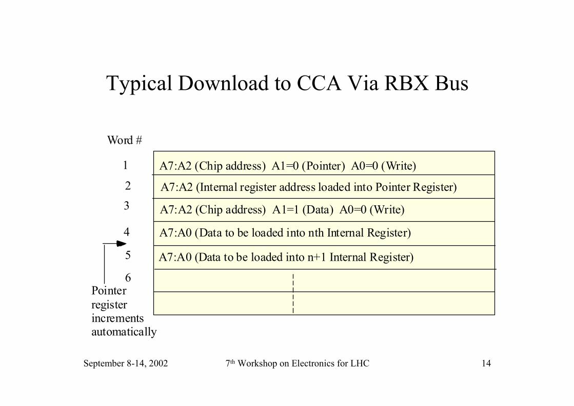
Typical Download to CCA Via RBX Bus
A7:A2 (Chip address) A1=0 (Pointer) A0=0 (Write)
A7:A2 (Internal register address loaded into Pointer Register)
A7:A0 (Data to be loaded into nth Internal Register)
A7:A2 (Chip address) A1=1 (Data) A0=0 (Write)
A7:A0 (Data to be loaded into n+1 Internal Register)
Word #
1
23
4
5
6Pointerregisterincrementsautomatically

September 8-14, 2002 7th Workshop on Electronics for LHC 15
Delay Locked Loop
• Delay LockedLoop has 25one nsec tapsto provide finecontrol of QIEclocks
• Each tap stageis comprisedof 2 inverters
1 25
25 to 1 Multiplexer
PhaseDetector
ChargePump
LoopFilter
QIEClock4
Delayselect
Control voltageInputclock

September 8-14, 2002 7th Workshop on Electronics for LHC 16
QIE Data Alignment and Transmission
• Bits from ControlRegister set 4 muxsin Data Alignmentblock for properdata alignment
• Cap IDs arechecked for propersynchronization
• Data Mux sendseither Orbitmessage or QIEdata at 40 MHz
QIE_EXPaQIE_MANTaQIE_CAPIDa
QIE_EXPbQIE_MANTbQIE_CAPIDb
FromQIEa
FromQIEb
LHC_CLOCK
QIE DataAlignment
DataMux
QIECap IDCheck
Sync_CapIDa
Sync_CapIDb
CapIDerror
QIE DATA 18
TX_DATA
SEND FF
CNTRL
DATA
Signalsto GOL
LHC_CLOCK
Mux controls
Orbit message
Controls from alignment register 7
18
18
2
22
2
2
2
5
5

September 8-14, 2002 7th Workshop on Electronics for LHC 17
Typical Data Transmission• When Bunch
Crossing Zero isreceived, anOrbit Message issent and at thesame time theQIEs are resetwith Cap ID=0.
• QIE data is sentafter the OrbitMessage
Cap ID error(1) Bunch error(1)Crossing number(12)Fill Frame(18 ones)
Data (18 bits)
Data (18 bits)
Irrelevant(4)
Fill Frame(18 ones)
Data (18 bits)
0
1
6970
35623563
Next Orbit MessageOrbitmessage
QIE Data
Orbitmessage
Word Count

September 8-14, 2002 7th Workshop on Electronics for LHC 18
Other CCA Circuits• Bunch Counter – 12 bit counter that starts at 0 and increments with
the LHC clock. Before reset at next Bunch Crossing=0, counter valueis compared to expected value in the Event Checker. Any errors areflagged. The BC value is also stored for transmission in Orbit Message
• Test Pulse Trigger Comparator – Produces a Send_Test_Pulsesignal when number in the Test Pulse Bunch Count Match Registerequals the Bunch Counter number. Pulse is 1 cycle long. Polarity issettable through a bit in the Control Register.
• Synchronizer – Synchronizes test pulses for the 2 QIE which havedifferent clock delays so the test pulse occurs in the same time slice.Also Syncs QIE reset pulses.

September 8-14, 2002 7th Workshop on Electronics for LHC 19
QIE
_EX
PaQ
IE_M
AN
TaQ
IE_C
API
Da
QIE
_EX
PbQ
IE_M
AN
TbQ
IE_C
API
Db
From
QIE
a
From
QIE
b
LHC
_CLO
CK
QIE
Dat
aA
lignm
ent
Dat
aM
uxQ
IEC
apID
Che
ck
Sync
_Ca
pID
a
Sync
_C
apID
b
CapI
Der
ror
QIE
DAT
A18
TX_D
ATA
SEN
DFF
CNTR
L
DAT
A
Sign
als
toG
OL
LHC
_CLO
CK
Mux
cont
rols
Con
trols
from
alig
nmen
treg
iste
r7
18
Add
ress
Dat
aR
BX_P
oint
erR
BX
_DAT
A
RBX
Bus
Inte
rfac
eCo
ntro
lReg
iste
rSpa
ceR
BX
CLK
RBX
_DAT
AC
ontro
lReg
iste
r(8
diffe
rent
cont
rolf
unct
ions
)
CA
LIB
_MO
DE
EN_Q
IER
AN
GE
QIE
_RA
NG
E
Alig
nmen
tR
egis
ters
Pede
stal
DA
CR
egis
ter
4
DLL
Tap
Sele
ctRe
giste
rQIE
a
DLL
Tap
Sele
ctRe
giste
rQIE
b
QIE
aCL
Km
ux
PED
_DA
CaPE
D_D
AC
bQ
IE_C
LKa
QIE
bCL
Km
ux
QIE
_CLK
b
Test
Puls
eB
unch
Mat
chR
egis
ters
Test
Patte
rnR
egis
ters
(20)
Del
ayLo
ckLo
op
LHC
cloc
k
Orb
itM
essa
ge
Bun
chCo
unte
r(1
2bi
ts)
Even
tSyn
cCh
eck
BC_
ZER
O
Bun
chC
ount
Sync
Erro
r
Test
Puls
eTr
igge
rC
ompa
rato
r
12Se
ndte
stpu
lse
QIE
RES
ETa
QIE
RESE
Tb
TEST
PULS
Ea
TEST
PULS
Eb
LHC
_CLO
CK
BC_Z
ero
Synchronizer
Enab
lePo
larit
y
BC
_Zer
oSe
ndFi
llFr
ames
Sele
ctO
rbit
Mes
sage
sour
ce
7
2 4 4
5 5
RBX
Add
ress 2 5 2 2 5 2
2 2
18
6
2 2
Sign
als
to QIE
s
CC
Aad
dres
sis
setb
y6
hard
wire
conn
ectio
nson
PCbo
ard

September 8-14, 2002 7th Workshop on Electronics for LHC 20
CCA chip
• Aligent 0.5 uCMOS process
• 3.4 x 4.0 mmdie
• 128 QFP, 14 x20 mm
• Production runof 11400 parts(22800channels)

September 8-14, 2002 7th Workshop on Electronics for LHC 21
Test Data
• 500 parts packaged for testing• 21 separate tests in test program• 200 parts measured to set cuts in test
program for power supply current (+/-15%) and delay time (+/- 2 ns)
• 227 parts were tested with cuts• 222 good parts for yield of 97.8%• Remaining 10, 900 parts to be packaged

September 8-14, 2002 7th Workshop on Electronics for LHC 22
Conclusion
• Production quantity of CCA has beenreceived for the Hadron Calorimeter
• All performance specifications have beenmet
• The CCA has been successfully run on aFront End Module with the QIEs
• The yield from testing the first 200 parts isvery high.

September 8-14, 2002 7th Workshop on Electronics for LHC 23
Acknowledgements
• The authors want to thank– Abder Mekkaoui for significant contributions
throughout the development of the CCA– William Wester and Christian Gingu in the
ASIC test group at Fermilab for the yieldinformation that was used
– Jim Hoff and Alpana Shenai for layoutassistance
– Al Dyer for his test assembly assistance