centre for large area flexible...
TRANSCRIPT
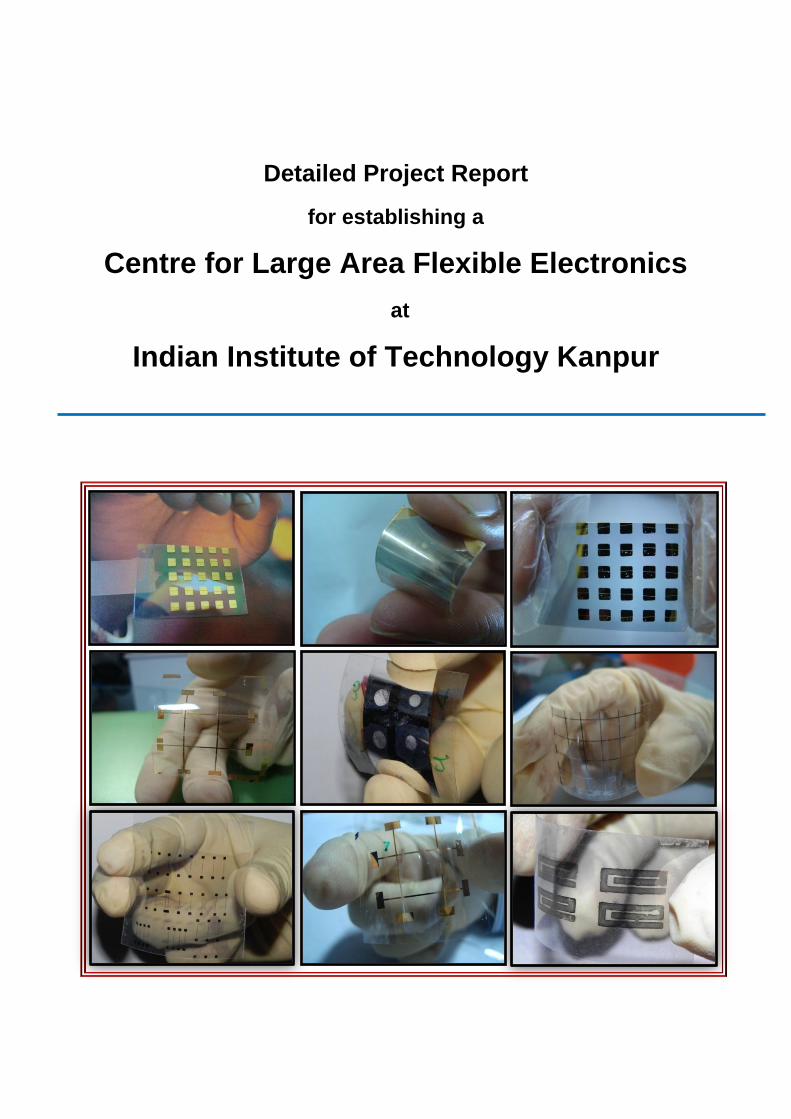
Detailed Project Report
for establishing a
Centre for Large Area Flexible Electronics
at
Indian Institute of Technology Kanpur
i
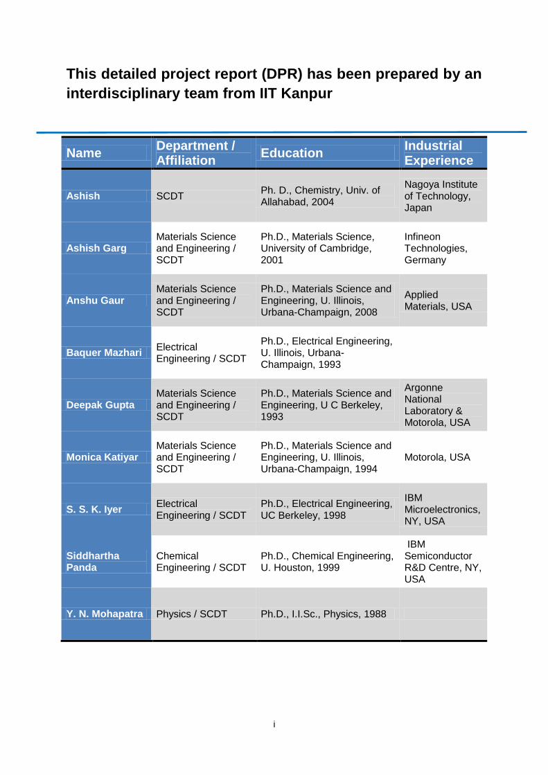
This detailed project report (DPR) has been prepared by an
interdisciplinary team from IIT Kanpur
Name Department / Affiliation
Education Industrial Experience
Ashish SCDT Ph. D., Chemistry, Univ. of Allahabad, 2004
Nagoya Institute of Technology, Japan
Ashish Garg Materials Science and Engineering / SCDT
Ph.D., Materials Science, University of Cambridge, 2001
Infineon Technologies, Germany
Anshu Gaur Materials Science and Engineering / SCDT
Ph.D., Materials Science and Engineering, U. Illinois, Urbana-Champaign, 2008
Applied Materials, USA
Baquer Mazhari Electrical Engineering / SCDT
Ph.D., Electrical Engineering, U. Illinois, Urbana-Champaign, 1993
Deepak Gupta Materials Science and Engineering / SCDT
Ph.D., Materials Science and Engineering, U C Berkeley, 1993
Argonne National Laboratory & Motorola, USA
Monica Katiyar Materials Science and Engineering / SCDT
Ph.D., Materials Science and Engineering, U. Illinois, Urbana-Champaign, 1994
Motorola, USA
S. S. K. Iyer Electrical Engineering / SCDT
Ph.D., Electrical Engineering, UC Berkeley, 1998
IBM Microelectronics, NY, USA
Siddhartha Panda
Chemical Engineering / SCDT
Ph.D., Chemical Engineering, U. Houston, 1999
IBM Semiconductor R&D Centre, NY, USA
Y. N. Mohapatra Physics / SCDT Ph.D., I.I.Sc., Physics, 1988
ii
Executive Summary
Large area electronics is a segment of electronics which is based on the monolithic
integration of electronic components on amorphous substrates which typically results in
products that are large in size with length scales ranging from a few centimeters as in
sensors, to a few decimeters as in displays and lighting, to several meters as in organic solar
cell based panels. This is in contrast to conventional microelectronics where integrated
circuits (ICs) are fabricated on crystalline substrates and length scales are typically only a
few millimeters.
Large area electronics is on the threshold of an imminent revolution that is driven by
innovative applications made possible at a much lower cost than conventional methods of
manufacturing. At the heart of this revolution lie two significant capabilities: designing
products that are flexible and form fitting, and their manufacturing by printing based
processes. The combination of the two may lead to roll-to-roll, large volume and high
throughput manufacturing.
This revolution is being driven by use of new materials and methods of
manufacturing. Hence, a break from the past has provided an opportunity to those who
missed the “microelectronic bus” earlier. In other words, there are no well established
players in flexible electronics at the moment and even those who are actively involved have
been in it for a relatively short period. The Indian industry must make use of this opportunity
to get a foothold in the emerging market for large area flexible electronics.
The electronics emerging from this would be fabricated on substrates that are
plastics, paper, textiles or metal foils. The circuits will be printed roll-to-roll by fast
manufacturing processes, much the same way as newspapers are printed. The products will
be much more affordable and if required, even disposable. They find applications in several
sectors of industry and technology. To name a few, distributed energy production through
organic solar cells on windows and roofs, disposable sensors for air and water quality
management or lab-on-a-chip for health monitoring, security packaging of medicines to
check circulation of fake drugs, wearable and lightweight electronics on textiles as a soldier’s
gear, airport baggage handling, labeling of books in libraries or answer scripts in a large
scale examination, flexible displays and lighting. Clearly, the examples span a large number
of industrial sectors, and point to the widely held belief that only imagination is the limit to
possible applications.
According to global industry sources, the flexible electronics market in 2011 was
USD 1.8 billion and projected to be USD 19 billion in 2018. Much of the activity today is
concentrated in the USA in North America; Germany, Finland and Denmark in Europe; and
Korea, Taiwan and Japan in East Asia. In these locations, the development has
accompanied emergence of several large sized strategic alliances and centres of
excellence. A number of industry dominated conferences in flexible electronics have begun
to see participation in excess of 1500 persons. The time is ripe for the Indian industry to
take note of this rapidly emerging technology.
Since the domain of large area electronics today is still research driven, academic
leadership is a must. However, in the Indian context, in order to reduce time to market, it is

iii
necessary to have simultaneous industrial participation. Further, the strategy for the
development of manufacturing in flexible electronics in India should jointly emerge from a
tripartite participation of industry, academia and government. Such issues should be
addressed through a centre for excellence in flexible electronics. An interdisciplinary team of
researchers at IIT Kanpur who have the required experience and expertise in the area
propose to set up such a centre.
The vision of the centre is to conduct research and development in large area flexible
electronics that serves as a foundation for development of domestic industry in this field. To
achieve the vision, the objectives are to simultaneously conduct basic studies in the
academia and develop products with (and also for) the industry. Further, one of the
important objectives of the centre will be to facilitate up-front interaction of all segments of
the industry - product, materials and equipment - during the development cycle itself, in
accordance to a mutually shared road map for commercialization. In addition, the centre will
promote small scale entrepreneurship, build national and international linkages and raise
human resources in flexible electronics.
To realize these objectives, a centre, named as FlexE Centre, has been
conceptualized as a platform having state of the art infrastructure and a competent team,
named FlexE Team, entrusted with functions of generating knowledge, demonstrating proof
of concept and build prototypes. The FlexE Team will serve as the link between the
knowledge generation activity of academic partners and prototype and product building
activities of industrial partners.
The model proposed for rapid development is a foundry-like structure. A flexible
electronics based product is likely to have one or more of elements, such as transistors,
memories, diodes, passive components, sensors, actuators (displays, LEDs, loudspeakers),
power generation sources (photovoltaics) and energy storage elements (batteries). The
centre will identify the state-of-art in these components, establish the component
specifications and realize the components of these specifications. The industry will design
products of their choice and rapidly build prototypes with these components. Wherever
modifications and improvements of the specifications are required, the FlexE Team and
industry will develop them together. New innovations and paradigm shifts in component
technology will be the joint responsibility of academic partners and the FlexE Team.
Clearly, the FlexE team constitutes the heart of the FlexE Centre and therefore, it is
imperative that the team should be of appropriate quality and size. To attract quality
manpower, we propose to use industry participation and deputation of its personnel to the
FlexE Team with attractive options to acquire higher educational degrees. The team would
need a variety of expertise such as in device development, systems integration, electronics
prototyping, materials and equipment support. Accordingly, the size of the team determined
is approximately 60 persons, led by professionals of considerable experience and
specifically hired to operate the centre.
Finally, it is critical that the FlexE Centre is supported with adequate funds in the
initial stages to help spawn entities spanning the whole manufacturing eco-system thereby
enabling the large area electronics technology to take root in India. The detailed project
proposal is laid out with all its components including deliverables, estimated costs of
establishing the centre and time schedules.

iv
Table of Contents
The Team at IIT Kanpur i
Executive Summary ii
1. Large Area Electronics 1
2. Flexible Electronics: The Way Forward 2
2.1 Major Applications of Large Area Flexible Electronics 4
2.1.1 Displays 4
2.1.2 Photovoltaic Applications 4
2.1.3 Printed Batteries 5
2.1.4 Large Area Flexible Sensors 5
2.1.5 Packaging Tags 5
2.1.6 Smart Labels & Printed RFID 5
2.2 Other Novel Applications 6
3. Flexible Electronics: Current Status and Projections 10
3.1 Global Market Scenario 10
3.2 Market Drivers 11
3.3 Strategic Alliances 12
3.4 Centres of Excellence 13
3.5 Conferences 14
4. Flexible Electronics: A Case for Academic Leadership 15
5. Vision and Objectives 17
6. Realising the Vision: A Framework 18
7. Functional Elements and their Role 20
7.1 Academic Ecosystem 20
7.1.1 The Facility and the Scientific Programme 20
7.1.2 Education and Training 21
7.1.3 Collaborations: Academic Partners and International Collaborations 21
7.1.4 Research Support to Academic Institutions 21
7.2 Industry Ecosystem: Products, Materials and Equipment 21
7.2.1 Product Industry 22
7.2.2 Equipment Industry 22
7.2.3 Materials Industry 22
8. Flexible Electronic Systems: The Scientific Programme 23
9. Organisational Structure and Processes 26
10. The Programme of Activities 31
10.1 Research and Development 31
10.1.1 Research 31
v
10.1.2 Development 31
10.2 Deliverables 32
11. Budget 34
11.1 Budget 34
11.1.1 Industry Contribution 34
11.1.2 IIT Kanpur Contribution 35
12. Potential Benefits to the Nation 36
13. Biographical Sketch of the IIT Kanpur Team 38
Annexure List 43
Annexure I Minutes of the workshop on “Centre of Excellence for Large Area Flexible
Electronics” held at IIT Kanpur on March 15, 2013
44
1
1. Large Area Electronics
Electronics includes a wide gamut of products and applications, the foundation of
which is the high-tech and high-value microelectronics industry.
Microelectronics normally conjures up an image of integrated circuits (ICs) and
silicon wafers and industry names such as Intel and AMD. This technology is implemented
on single crystal silicon wafers. Over time, conventional crystalline silicon based
microelectronic manufacturing has followed the concept of decreasing feature size (from
microns to nanometers) and increasing substrate size (from 2” wafers in the 1960s to 12”
today) to develop increasing complex ICs at competitive prices. Unfortunately, in the
commercial sector, manufacturing in this segment of industry in our country is nearly non-
existent.
However, there is another set of products within microelectronics that are built not on
crystalline silicon, but on glass and are equally large both by production volume and
revenue. These, for example, include displays/television, lighting and photovoltaic modules.
A television screen is made of pixels that are only tens of micrometers; thus making of a
television is in the domain of microelectronics. However, the sizes in which a consumer may
want the televisions are in excess of 40-60 inches. Further, to achieve lower costs, several
screens of television are made simultaneously on a single glass plate. Thus, the size scale
on which this segment of microelectronic industry works is in meters. Similarly, photovoltaic
panels based on thin film of amorphous or polycrystalline forms of silicon are made in sizes
that are in meters. Thus, these applications represent microelectronics on large area
substrates leading to the terminology, Large Area Electronics.
The limitations faced in the scaling up of substrate size in the manufacturing of these
traditional large area electronic systems can be overcome by printing organic and inorganic
materials on flexible substrates. The flexible substrate based manufacturing platforms would
not only lead to lower production costs, but also benefit applications that derive value from
the larger size of the systems.
We first illustrate the new possibilities in applications and the potential low cost of
such devices and then establish that the emergence of this field in the commercial sector is
imminent.

2
2. Flexible Electronics: The Way Forward
The electronic functions of control, logic, sensing, and information transmission
brings intelligence to all the products. The prospect of bringing this intelligence to all objects
without restricting it to electronic instruments which use high performance integrated circuits
has given rise to the potential for a complete range of new applications – literally bringing the
functionalities ‘out of the box’. The winning combination of features that characterize this
pervasive electronic based intelligence, also referred to as ‘electronics everywhere and for
everybody’, are:
a) flexible substrates such as plastic, paper, textiles and metal foils for all possible
forms,
b) printable circuits in large area possibly in roll-to-roll fast manufacturing processes
similar to mass printing of newspapers,
c) affordable, i.e., low cost functionalities with performance just enough and appropriate
for a particular application,
d) disposable after its designated duration of usage with possibility of recycling of
components
Large area flexible and printable electronics essentially implies the manufacturing of
electronic devices on a flexible substrate by employing printing techniques. High throughput
methods such as roll-to-roll processes ensure large volume production - and coupled with
the fact that a single line of machinery would be required in most cases - low cost and less
energy-intensive end products. From the environmental perspective, flexible electronic
products have the potential to be environment-friendly and biodegradable. In addition, lower
power consumption and light weight make them attractive candidates for military, space and
transport sectors. A technological revolution of sorts is in the making since it is going to
touch almost all aspects of our lives – in ways that we may not be able to fully imagine at this
point of time. We cite, as examples, some of the current developments and its progress
within the grand challenge areas of energy, health, environment, defence, communication,
transport and education.
It should be emphasized that this technology is truly relevant to India, both from the
point of view of potential applications as well as developing new paradigm for electronics
manufacturing. In contrast to conventional electronics, which involves capital intensive and
complex fabrication facilities, manufacturing in flexible electronics is likely to need less
capital and will be much simpler – which is ideal for distributed production. Hence, the
advent of this technology offers a level playing field and newer opportunities in many
sectors. Some of these are summarized below.
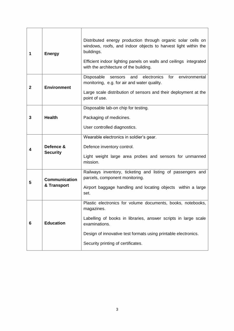
3
1
Energy
Distributed energy production through organic solar cells on
windows, roofs, and indoor objects to harvest light within the
buildings.
Efficient indoor lighting panels on walls and ceilings integrated
with the architecture of the building.
2 Environment
Disposable sensors and electronics for environmental
monitoring, e.g. for air and water quality.
Large scale distribution of sensors and their deployment at the
point of use.
3 Health
Disposable lab-on chip for testing.
Packaging of medicines.
User controlled diagnostics.
4 Defence &
Security
Wearable electronics in soldier’s gear.
Defence inventory control.
Light weight large area probes and sensors for unmanned
mission.
5 Communication
& Transport
Railways inventory, ticketing and listing of passengers and
parcels, component monitoring.
Airport baggage handling and locating objects within a large
set.
6 Education
Plastic electronics for volume documents, books, notebooks,
magazines.
Labelling of books in libraries, answer scripts in large scale
examinations.
Design of innovative test formats using printable electronics.
Security printing of certificates.

4
2.1 Major Applications of Large Area Flexible Electronics
The new emerging technology would spawn its own new areas of applications. A
myriad such applications have already been demonstrated and some of these have been
marketed also. Fields of displays PV, lighting, healthcare and transport are going to be
revolutionized in the next 5-10 years due to the adoption of printable and flexible electronics.
2.1.1 Displays
Displays are poised to be
the largest share of flexible
electronics products. It is
expected that while glass size
may limit the dimensions of
displays on glass, printed
displays on plastics will not have
such restrictions. Roll-to-roll
processes may increase the
volume of production and the
prices can be controlled. The
flexibility and the thin form factor
may add to the appeal of such
displays from a consumer’s perspective. Both industrial and academic groups are active in
flexible display development. For instance, the flexible display centre at Arizona state
university recently demonstrated the largest flexible OLED display.
2.1.2 Photovoltaic applications
Large area flexible electronics on
substrates such as steel are especially
attractive in countries such as India where
many shelters and godowns use corrugated
steel as roofs. Integration of solar cell
modules on the outer surface as power
generation source and white light emitting
diodes on the inner surface for lighting is
attractive for building and also adds
significant value to the roof. The picture on
the right shows a 144W building integrated photovoltaic (BIPV) flexible solar
panel.(http://imagesen.busytrade.com/176131800/144w-Flexible-Solar-Panel-For-Bipv.jpg).
Flexible photovoltaic modules can also find
innovative applications as in the awning
above car parks providing useful shade as
well as generating valuable power. Their low
weight and flexible nature make their
deployment easier and less costly.
Flexible OLED display(FraunhoferInstitute, Germany)
Flexible cell phone display (Samsung)

5
Integrating flexible electronics in fabric has potential for a
large number of applications. One application is a battery
charger integrated in clothes as seen on left (enfsolar.com).
This is particularly useful for defence applications as well
as for outdoor recreational activities. Many universities and
research labs have been exploring integrating PV in fabric.
For example, Colorado State University (CSU) is trying to
develop a natural fibre for outdoor clothing that can charge
portable devices.
2.1.3 Printed batteries
Smart objects such as RFIDs, stand-alone sensors, etc. require a power source
which should be thin, flexible and congenial to design requirements. Printed batteries meet
these challenges. In addition the common markets, they cater to the needs of niche
markets, such as, anti-wrinkle plasters. They provide options for many practical and novel
applications in combination with flexible photovoltaic modules.
2.1.4 Large Area Flexible sensors
Flexible sensors will have applications in many areas including military, security
enforcement, environmental monitoring, biomedical applications, robotics, packaging, etc.
Many industrial competitors are active in this area. Sony, Agilent, VTT, Plastic logics,
PARC, IMEC and Future Shape GMBH are some of the top players.
Sensors integrated with printed transistors on flexible sheets have been
demonstrated as artificial skin for robots with ability to sense pressure, temperature and
chemical environment.
2.1.5 Packaging tags
A temperature sensor integrated with a
timer can be used for monitoring perishable goods
and pharmaceutical products. This smart
packaging can collect data and wirelessly
communicate to a wider target audiance. Thin Film
Electronics, Norway is developing these smart
packaging to be commercialized by Bemis by 2014.
Such smart packaging will allow the user to walk
through with their trolley whilst a scanner reads the
goods and totals the amount, charges it to the
customer’s account and adjusts the shop’s
inventory.
2.1.5 Smart Labels & Printed RFID
The area in which large area electronics
has advanced the most at present is in
applications involving smart labels for objects
and identification. These include tens of
electronics-eetimes.com
Sunchon National University
6
thousands of items in retail stores, baggage sorting at airports, couriers, tickets, letters,
perishable items such as milk, fruits and meat, etc. This has given rise to the concept
termed as ‘internet of things’ in which objects made intelligent by fixing labels on them,
allows them to be queried, sorted, sold or controlled during transportation.
Though RFID tags are routinely being used, to achieve their complete potential, more
widespread use is essential. This can happen only if they come at a lower price and printing
leads to a cheap manufacturing process. PolyIc (Germany) is the pioneer in this field.
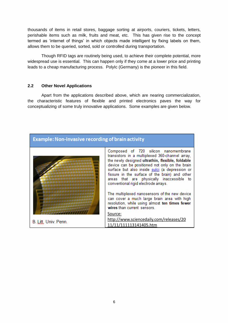
2.2 Other Novel Applications
Apart from the applications described above, which are nearing commercialization,
the characteristic features of flexible and printed electronics paves the way for
conceptualizing of some truly innovative applications. Some examples are given below.
Source: http://www.sciencedaily.com/releases/2011/11/111113141405.htm

7
Source: http://ucsdnews.ucsd.edu/archive/newsrel/general/20110707UnderwaterSensors.asp
8
This scenario has been made possible by a unique combination of newly acquired
capabilities over the last two decades. The key elements of such capabilities are:
i) functional design of molecules: a large set of material systems have been discovered
and continuing to be improved at break-neck speed,
ii) nanoscale-engineered materials for macro-scale processes such as printing,
iii) low temperature processes for realizing complex hetero-structures of different types
of materials from metals to semiconductors to dielectrics obtainable in thin film from,
iv) ability to design systems based on limited performance of components,
v) interdisciplinary expertise from diverse fields such as chemistry of materials and
inks, physics of thin films, new directions in materials engineering, chemical
engineering involving fluid dynamics of control of novel unit processes, electronics
and electrical engineering of component and system development requiring notions
different from the established microelectronics.
The various academic challenges stem from the issues listed above and one needs
innovation at many levels by pushing the existing boundaries of each of the disciplines
involved. Similarly developing applications whilst keeping the needs of different user
agencies in perspective require innovative technology development models, as well as new
business strategies.
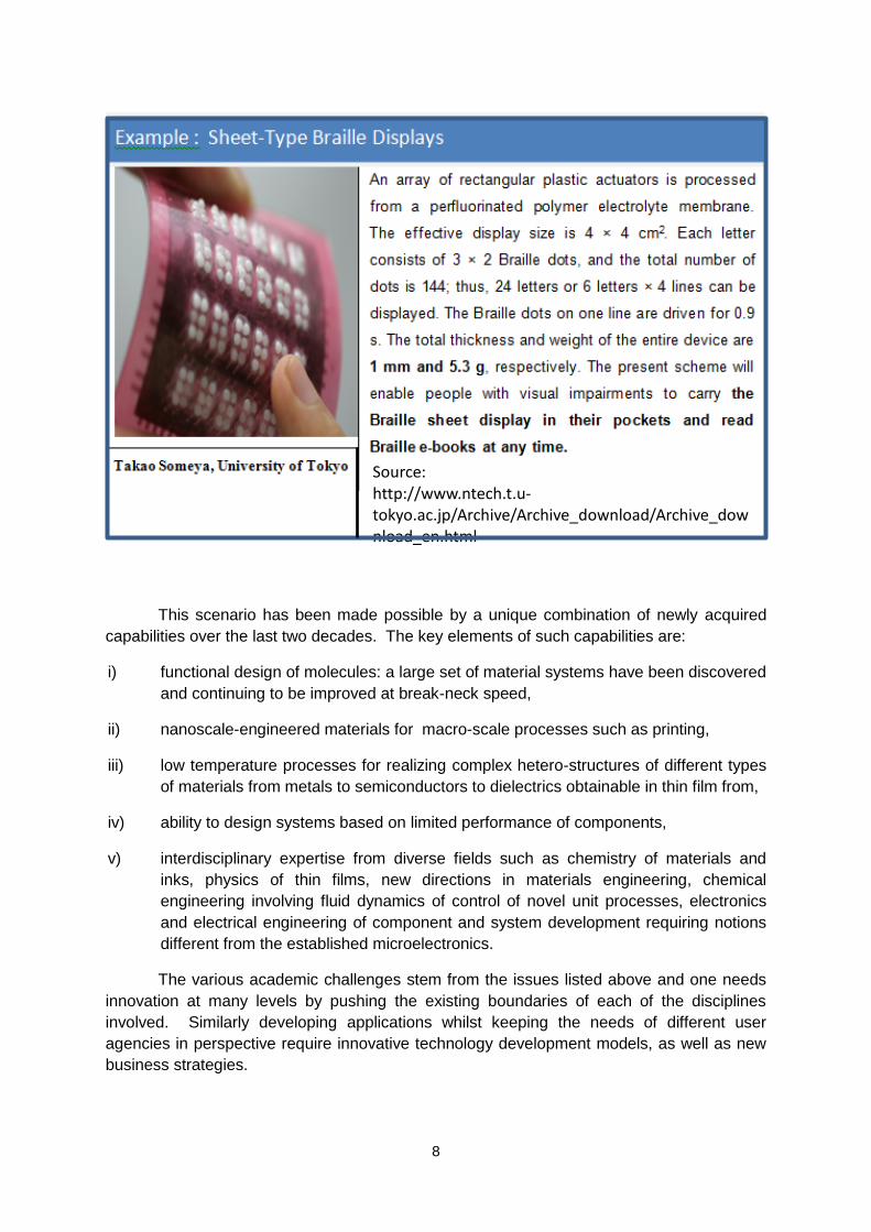
Source: http://www.ntech.t.u-tokyo.ac.jp/Archive/Archive_download/Archive_download_en.html

9
There have been seminal developments in the area, thanks to interdisciplinary
academic groups who have contributed on the one hand to the core intellectual challenges
involved, and on the other to nucleation of successful start-up companies sufficient to inspire
confidence in commercial investors.
10
3. Flexible Electronics: Current Status and Projections
3.1 Global Market Scenario
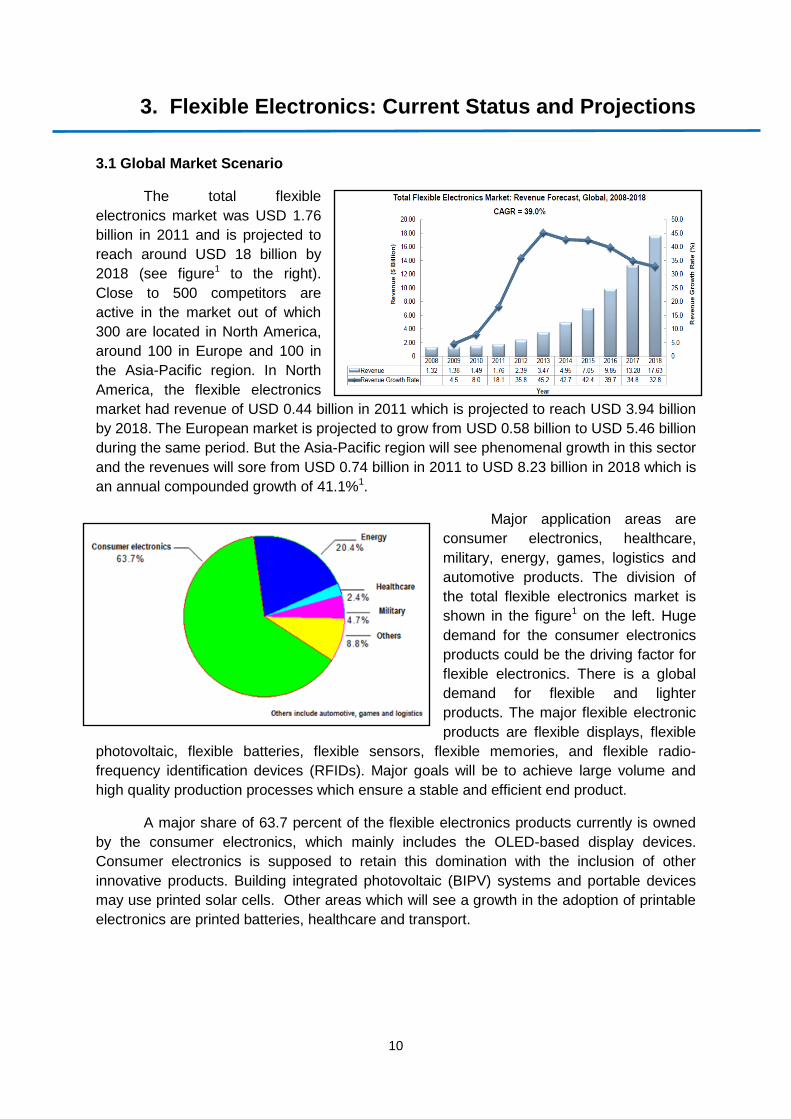
The total flexible
electronics market was USD 1.76
billion in 2011 and is projected to
reach around USD 18 billion by
2018 (see figure1 to the right).
Close to 500 competitors are
active in the market out of which
300 are located in North America,
around 100 in Europe and 100 in
the Asia-Pacific region. In North
America, the flexible electronics
market had revenue of USD 0.44 billion in 2011 which is projected to reach USD 3.94 billion
by 2018. The European market is projected to grow from USD 0.58 billion to USD 5.46 billion
during the same period. But the Asia-Pacific region will see phenomenal growth in this sector
and the revenues will sore from USD 0.74 billion in 2011 to USD 8.23 billion in 2018 which is
an annual compounded growth of 41.1%1.
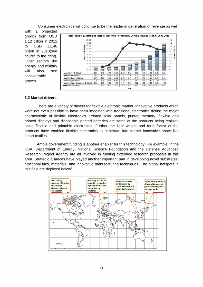
Major application areas are
consumer electronics, healthcare,
military, energy, games, logistics and
automotive products. The division of
the total flexible electronics market is
shown in the figure1 on the left. Huge
demand for the consumer electronics
products could be the driving factor for
flexible electronics. There is a global
demand for flexible and lighter
products. The major flexible electronic
products are flexible displays, flexible
photovoltaic, flexible batteries, flexible sensors, flexible memories, and flexible radio-
frequency identification devices (RFIDs). Major goals will be to achieve large volume and
high quality production processes which ensure a stable and efficient end product.
A major share of 63.7 percent of the flexible electronics products currently is owned
by the consumer electronics, which mainly includes the OLED-based display devices.
Consumer electronics is supposed to retain this domination with the inclusion of other
innovative products. Building integrated photovoltaic (BIPV) systems and portable devices
may use printed solar cells. Other areas which will see a growth in the adoption of printable
electronics are printed batteries, healthcare and transport.
11
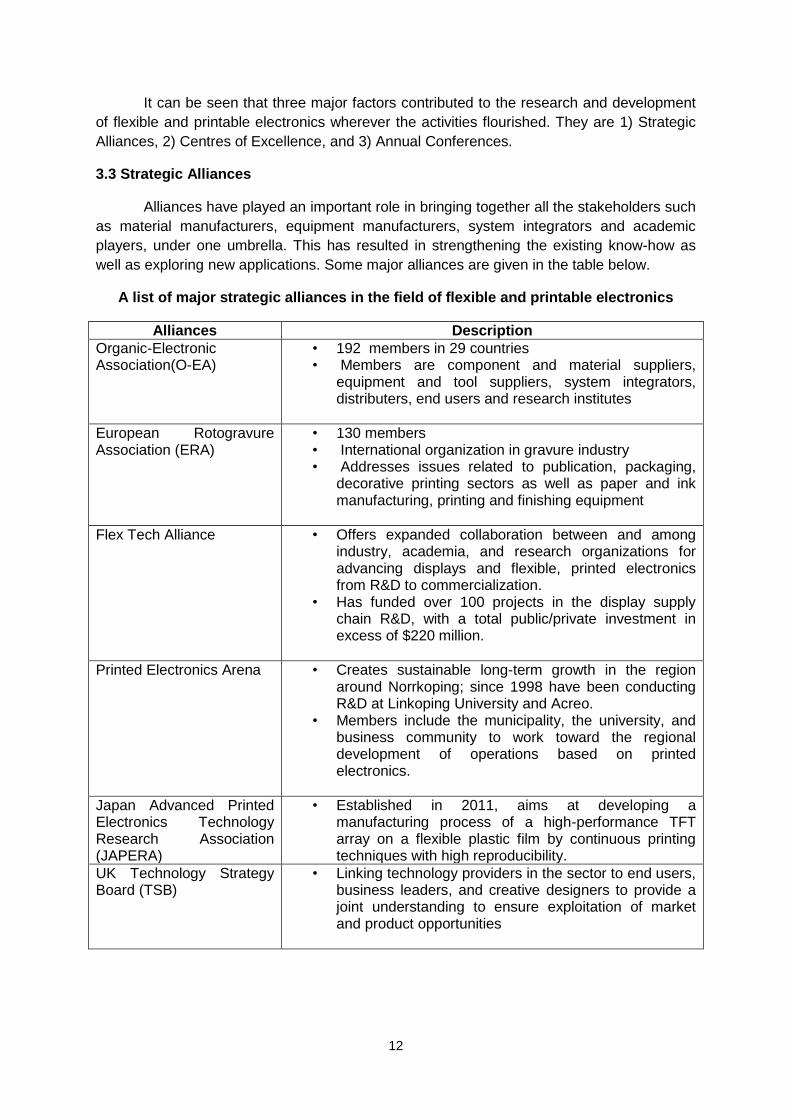
Consumer electronics will continue to be the leader in generation of revenue as well,
with a projected
growth from USD
1.12 billion in 2011
to USD 11.46
billion in 2018(see
figure1 to the right).
Other sectors like
energy and military
will also see
considerable
growth.
3.2 Market drivers
There are a variety of drivers for flexible electronic market. Innovative products which
were not even possible to have been imagined with traditional electronics define the major
characteristic of flexible electronics. Printed solar panels, printed memory, flexible and
printed displays and disposable printed batteries are some of the products being realized
using flexible and printable electronics. Further the light weight and form factor of the
products have enabled flexible electronics to penetrate into further innovative areas like
smart textiles.
Ample government funding is another enabler for this technology. For example, in the
USA, Department of Energy, National Science Foundation and the Defense Advanced
Research Project Agency are all involved in funding extended research proposals in this
area. Strategic alliances have played another important part in developing novel substrates,
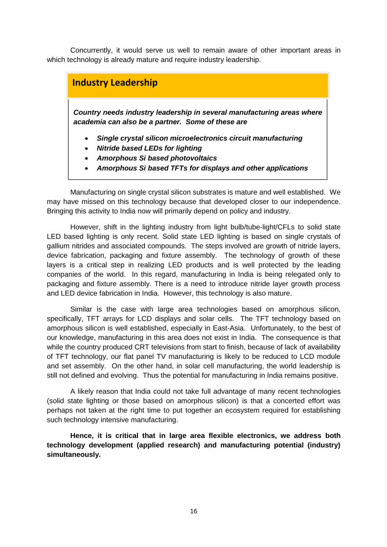
functional inks, materials, and innovative manufacturing techniques. The global hotspots in
this field are depicted below1.
12
It can be seen that three major factors contributed to the research and development
of flexible and printable electronics wherever the activities flourished. They are 1) Strategic
Alliances, 2) Centres of Excellence, and 3) Annual Conferences.
3.3 Strategic Alliances
Alliances have played an important role in bringing together all the stakeholders such
as material manufacturers, equipment manufacturers, system integrators and academic
players, under one umbrella. This has resulted in strengthening the existing know-how as
well as exploring new applications. Some major alliances are given in the table below.
A list of major strategic alliances in the field of flexible and printable electronics
Alliances Description
Organic-Electronic Association(O-EA)
• 192 members in 29 countries • Members are component and material suppliers,
equipment and tool suppliers, system integrators, distributers, end users and research institutes
European Rotogravure Association (ERA)
• 130 members • International organization in gravure industry • Addresses issues related to publication, packaging,
decorative printing sectors as well as paper and ink manufacturing, printing and finishing equipment
Flex Tech Alliance
• Offers expanded collaboration between and among industry, academia, and research organizations for advancing displays and flexible, printed electronics from R&D to commercialization.
• Has funded over 100 projects in the display supply chain R&D, with a total public/private investment in excess of $220 million.
Printed Electronics Arena
• Creates sustainable long-term growth in the region around Norrkoping; since 1998 have been conducting R&D at Linkoping University and Acreo.
• Members include the municipality, the university, and business community to work toward the regional development of operations based on printed electronics.
Japan Advanced Printed Electronics Technology Research Association (JAPERA)
• Established in 2011, aims at developing a manufacturing process of a high-performance TFT array on a flexible plastic film by continuous printing techniques with high reproducibility.
UK Technology Strategy Board (TSB)
• Linking technology providers in the sector to end users, business leaders, and creative designers to provide a joint understanding to ensure exploitation of market and product opportunities

13
3.4 Centres of Excellence
During the last few years several research centres focused on flexible and printable
electronics sprouted in USA, Europe and the Far East. Most of them are government-funded
and they provide a common platform for several industrial and academic players to work
together. A representative list of such centres is given below.
Representative list of centres for R&D in flexible and printable electronics
Centre Description
Flexible Display Center, Arizona State University (http://flexdisplay.asu.edu)
Main focus is on flexible OLED displays. Different levels of membership are offered to industrial partners. Currently having 23 industrial partners, 5 government partners and 3 academic partners. Has mass manufacturing capability.
Flexible Electronics Research Center, AIST, Japan (http://unit.aist.go.jp/flec/index_en.html)
Developing components, manufacturing technology and evaluation standards. Five functional teams are actively engaged in research.
Holst Centre, Netherlands (http://www.holstcentre.com)
Develops generic technologies for wireless autonomous sensor arrays. With 35 industrial partners the centre has shared roadmaps and programmes.
Centre for Plastic Electronics, Imperial College, UK
An interdisciplinary team from Imperial College London coordinates the activities. The doctoral training centre is an attraction for industrial partners. Aim is to ensure UK’s dominant position in plastic electronics.
VTT Printed Intelligence, Finland (www.cpi.vtt.fi)
Vision is to employ low-cost and easy to use printed components for light emitting surfaces, sensing, energy foils, optical films etc. Facilities include various roll-to-roll fluid printing and coating labs and pilot scale equipments. Entrepreneurial activities also undertaken.
Institute for Print & Media Technology Chemnitz University of Technology (www.tu-chemnitz.de/pm)
Has developed multifunctional printing capabilities. Developing mass printing technologies for photovoltaic, sensor, communication segments.
Korea Printed Electronics Center(KPEC) (www.printedelectronicskorea.org)
Established by KETI. Establishing core technologies for printed electronics. Nurturing industrial cluster.
Printable Electronics Research Center, Suzhou, China (http://perc-sinano.com/en/)
Established by Chinese academy of Sciences. First research centre on printed electronics in China. Focuses on early stage product development and prototyping in PV, TFT and OLED

14
3.5 Conferences
Annual conferences play a vital role in arranging the venue for discussing the state-
of-the-art technology, showcasing the prototypes and presenting the technology roadmaps.
Some of the major annual conferences in the field of flexible and printable electronics are
listed below. The number of conferences and participants in it are an indicator of worldwide
interest.
Major annual conferences in the field of flexible and printable electronics.
Conference Details
LOPE-C (Large area organic and printed electronics convention)
Annual conference organized by Organic and Printed Electronics Association(OE-A) and Messe Munchen International(Germany) In 2012, there were around 1500 participants from 46 countries
IDTechEx conferences Printed Electronics Asia Printed Electronics Europe
Many end-user application segments have their presence Main focus is on the commercialization of the technology
Flexible and printed electronics conference Organized by Flextech alliance in USA More than 300 organizations present their technologies, roadmaps and forecasts
Printed Electronics, China Organized by Chinese Academy of Sciences and the Ministry of Science and Technology
References
1. Future of semiconductors in flexible electronics market: Frost & Sullivan analysis,
NAF-27, August 2012.
2. Printed organic and flexible electronics forecast: Players and opportunities, IDTechEx
Report: 2009-2029.

15
4. Flexible Electronics: A Case for Academic Leadership
Manufacturing in microelectronics may be divided in two categories, (a) that on single
crystal substrates, limited to a maximum size below 30 cm and (b) that on large area
substrates, mostly with amorphous or polycrystalline materials, on meter scale or roll-to-roll .
As the innovations in applications suited for large area flexible electronics and current
trends for it indicate, fortunately, we stand at a cusp in time, where the existing large area
electronics industry is undergoing major changes. That provides renewed opportunities in
India, at the levels of both innovation and manufacturing. The demand for better
performance in existing products and new applications is being met by the introduction of
new materials or innovative products. The consequences of these changes are illustrated
below by two examples.
To date, the workhorse of the thin film transistor (TFT) industry for displays has been
amorphous silicon. However, demand for better performance from displays is exceeding
those that can be delivered by amorphous silicon. To meet the challenge, search for
alternatives is leading to materials such as indium gallium zinc oxide. This represents an
opportune time for India to enter into manufacturing, as the shift to new material represents a
leveling of competitive landscape to a certain extent.
In addition to new materials, as we have shown in the previous sections, applications
in the large area electronic segment are moving towards flexible and form fitting devices.
This demand also forces new methods of processing, especially by introduction of printing
as a means to fabricate electronic circuits. This impending change also offers India an
opportunity to claim a portion of the manufacturing pie. An illustrative example is the field of
LED lighting. While we are significantly behind in single crystal based LED lighting and
international industry is well established, the emerging technology of organic light emitting
diodes (OLED) on a large area and in a flexible form offers an opportunity to break the entry
barrier to manufacturing in the LED based lighting segment.
These two examples clearly illustrate that the search for new materials and new
methods of manufacturing are research driven and hence will require a leadership role from
academia. Both academia and industry need to come together in a mission mode for
ensuring manufacturing activities in the country.
Large area electronic manufacturing is in transition with new materials and
methods of manufacturing. This transition offers us a window of opportunity.
Further, as the transition is necessarily research driven, the role of academia is
important. Hence, large area electronics in general and flexible electronics in
particular, is an area ripe for academia driven academia-industry-government
collaboration to usher in flexible electronics manufacturing in India.
The Flexible Way: Academic Leadership
16
Concurrently, it would serve us well to remain aware of other important areas in
which technology is already mature and require industry leadership.
Manufacturing on single crystal silicon substrates is mature and well established. We
may have missed on this technology because that developed closer to our independence.
Bringing this activity to India now will primarily depend on policy and industry.
However, shift in the lighting industry from light bulb/tube-light/CFLs to solid state
LED based lighting is only recent. Solid state LED lighting is based on single crystals of
gallium nitrides and associated compounds. The steps involved are growth of nitride layers,
device fabrication, packaging and fixture assembly. The technology of growth of these
layers is a critical step in realizing LED products and is well protected by the leading
companies of the world. In this regard, manufacturing in India is being relegated only to
packaging and fixture assembly. There is a need to introduce nitride layer growth process
and LED device fabrication in India. However, this technology is also mature.
Similar is the case with large area technologies based on amorphous silicon,
specifically, TFT arrays for LCD displays and solar cells. The TFT technology based on
amorphous silicon is well established, especially in East-Asia. Unfortunately, to the best of
our knowledge, manufacturing in this area does not exist in India. The consequence is that
while the country produced CRT televisions from start to finish, because of lack of availability
of TFT technology, our flat panel TV manufacturing is likely to be reduced to LCD module
and set assembly. On the other hand, in solar cell manufacturing, the world leadership is
still not defined and evolving. Thus the potential for manufacturing in India remains positive.
A likely reason that India could not take full advantage of many recent technologies
(solid state lighting or those based on amorphous silicon) is that a concerted effort was
perhaps not taken at the right time to put together an ecosystem required for establishing
such technology intensive manufacturing.
Hence, it is critical that in large area flexible electronics, we address both
technology development (applied research) and manufacturing potential (industry)
simultaneously.
Country needs industry leadership in several manufacturing areas where
academia can also be a partner. Some of these are
Single crystal silicon microelectronics circuit manufacturing
Nitride based LEDs for lighting
Amorphous Si based photovoltaics
Amorphous Si based TFTs for displays and other applications
Industry Leadership
17
5. Vision and Objectives
Conduct research and development in large area flexible electronics that serves as a
foundation for development of domestic industry in this field.
Vision
R&D: Conduct basic studies and scientific investigations relevant to field of large
area flexible electronics.
Manufacturing: Conduct research and development in large area flexible
electronics by developing partnership with industry and with a view that potentially leads to manufacturing.
Ecosystems: Facilitate formation of industrial ecosystem by addressing various
aspects, products, materials and machines and academic ecosystem by engaging with reputed centers internationally and individuals nationally.
Entrepreneurship: Incubate small scale industry related to flexible electronics
International Partnerships: Build strategic partnerships that hasten the
development cycle.
Human Resources: Undertake human resource development in relevant area.
Objectives

18
6. Realising the Vision: A Framework
To realise the vision and meet the objectives, the conceptual structure of the centre
should include the following:
Around these core activities will be specific models for establishing strategic alliances
with international partners for education and training.
Apart from physical and functional elements of the centre, it is also important to
establish proper organizational structure and processes which promote the envisaged
interaction between academia and industry and among industries, while maintaining proper
checks and balances.
Based on the requirements described above, a concept of a centre has been
visualized and shown in the figure on the following page. It is to be noted that there are two
ecosystems. The first being an Academic Ecosystem comprising of Academic Partners and
International Collaborations engaged in Research, Education and Training. The second
ecosystem is an Industrial Ecosystem that brings together Products, Materials and
Equipment industries in one physical location. An important aspect of this concept is a tight
integration of all critical elements at one location to establish close Academia-Industry
Collaboration for realizing the goal of high impact R&D, new manufacturing industry and
entrepreneurship. As a consequence, the entity would necessitate the formation of a pan-
Indian team of academic experts to deliver R&D solutions for rapid development of large
area flexible electronic technologies.
The conceptual structure of the proposed centre is further elaborated in next few
pages.
dd
an interdisciplinary team that advances the frontiers of research in large area
flexible electronics.
state-of-the-art processing facilities operated by trained staff, making it
attractive to the industry for participation in developing products.
a platform for a meaningful interaction between industry and academia.
synergistic interaction among industries engaged in product development,
materials and equipment manufacturing.
Salient Features

19
20
7. Functional Elements and their Role
7.1 Academic Ecosystem
The goals of the academic ecosystem conceived here in the context of developing
flexible electronics, is to provide high quality research, provide education/training to generate
human resource, build academic collaborations, national and international, and participate in
strategic alliances. Accordingly, this ecosystem will be organized with the functional
elements described in the following sub-sections.
7.1.1 The Facility and the Scientific Programme
In the concept diagram, this element is described as “FlexE Centre” which will be a
state-of-the-art facility for flexible electronics. The role of IIT Kanpur will be to establish and
nurture it. It will be led by a group of faculty members drawn from interdisciplinary areas; a
brief profile of participating faculty is attached later in this document.
The equipment requirement in the centre will be derived from what is necessary to
produce flexible OLED lighting, photovoltaic and sensor array prototypes. This approach
will enable enough options to conceive other sets of product prototypes and fabricate them.
The intent for following this approach is to make the FlexE Centre attractive for industry to
take up prototyping activities.
The centre itself will be run by a competent staff. The scientific goal of this staff,
organized as “FlexE Team,” will be to establish processes to make good quality passive
components, OLEDs, TFTs, solar cell, batteries, sensors and encapsulation of flexible
substrates which can then be integrated to make product prototypes by the industry.
Another role of the FlexE Team would be to provide electronic design and system
integration. The capacity built by FlexE Team would also enable post-graduate research to
flourish. Further, this research would be tailored, when necessary, to suit the industry
requirements. Further details of the scientific programme are provided in the section:
Flexible Electronic (FlexE) Systems: The Scientific Programme. In short, led by a group of
faculty, the FlexE Team and the students from IIT Kanpur and other institutions across the
country will produce original research and facilitate rapid prototype development with
industry.
An important feature we wish to implement is with respect to deploying quality
manpower in the FlexE Team. The normal mechanisms available are to employ scientific
staff on established scales on short contracts, which either makes it unattractive for a
competent engineer/scientist or the turnover of such staff too frequent. To overcome this
problem, we intend to use the collaboration with industry as a means to deploy engineers on
their payrolls (existing or especially recruited) as part of their contribution towards the
partnership with the centre.
The core group of faculty at IIT Kanpur will evolve a policy for providing research
support for other academic institutions in the country. The same team will be responsible to
establish academic partners within country, international collaborations, training and
education and policy for interaction with the industry.
21
7.1.2 Education and Training
Along with the development of flexible electronics, it will be necessary to produce
trained manpower. As the centre is embedded in IIT Kanpur, the interested students will be
offered courses in this area. In addition, the faculty associated with the centre will
endeavour to attract large number of students to conduct research in flexible electronics as
part of their M.Tech. and Ph.D. programme.
Additionally, there will be an annual short course and periodic workshops organized
in large area and flexible electronics open to researchers and students from across the
country.
An attractive feature will be provision of post graduate (M. Tech. or Ph.D.) degree for
participants from the industry who work at the centre either as a part of FlexE Team or
collaborative projects with the industry. This would help in attracting the best persons from
industry to participate in the centre, while they retain their original employment status.
7.1.3 Collaborations: Academic Partners and International Collaborations
As part of academic outreach, we would leverage the services of best
engineers/scientists in the country working in the area of flexible electronics by establishing
partnerships with them and their institutions.
International Collaborations are important to provide visibility and also to learn the
best practices. On the academic front, IIT Kanpur already has an ongoing collaboration with
TU Chemnitz, Germany, for mass printable electronic products on paper and a leading
government research lab CSIRO, Clayton in Australia, in organic photovoltaic technologies.
Apart from that, there are several other centres with which opportunities of collaboration are
being explored. To name a few, these are Flexible Display Center, Arizona, Center for
Organic Photonics and Electronics (COPE), Georgia Tech, Center for Hierarchical
Manufacturing, University of Massachusetts, Amherst, Microelectronics Center, UT Austin,
and Microall in USA.
Further, there are a few strategic alliances forming between a group of industries and
research centres. It is important to be a part of such alliances not only to gain access to
technology, but also to play a role in the definition of standards.
7.1.4 Research Support to Academic Institutions
Wherever possible, the FlexE Team will provide assistance to individuals from other
academic institutions for carrying out their research at the centre.
7.2 Industry Ecosystem: Products, Materials and Equipment
It will be natural for the centre to interact with industry that would be making final
products, such as photovoltaic modules and OLED lighting sources. However, experience
suggests that even when successful prototype development takes place, product
manufactures are reluctant to commercialise the product due to the risks associated with the
import of equipment and materials. In the absence of an existing domestic market, the
equipment and materials companies, despite having the requisite skills also remain reluctant
to invest.
22
Therefore, it is necessary to ensure simultaneous engagement with product,
equipment and materials industries. This is best served by establishing a mechanism that
brings their representatives together. As indicated in the concept diagram, the FlexE Centre
intends to provide this much needed platform, and bring together the three types of
industries to interact among themselves and with the academic part of the centre.
7.2.1 Product Industry
The centre through its FlexE Team would undertake development of critical set of
components, such as resistor, capacitor, inductor, TFT, OLED, solar cell, etc. The product
industry will interact with the centre as a Partner (described in section Organizational
Structure and Processes) and execute projects with IIT Kanpur. The goal will be to build
prototypes of commercial products using the components developed. The largest effort of
the centre with respect to interaction with the industry will be focused here.
7.2.2 Equipment Industry
We will identify equipment makers who at a small scale have provided quality
products for R&D in microelectronics and have them open a cell at IIT Kanpur within the
centre. The objective will be to identify, among all the equipment needed, the ones that
should be developed first. The decision will be based on capability, ease and requirements
of the product industry.
Projects will be initiated to develop these equipments. The design will be researched
at the centre, but fabrication activity will be external, according to the design developed at
the centre. Thus laboratory facility required for this industry will be in form of a computer
laboratory only. An important objective of including this activity will also be to initiate small
scale enterprises by students in IIT Kanpur.
7.2.3 Materials Industry
Two types of activities will be encouraged with materials industry. The first will be to
facilitate kilogram or higher level production of established and proven materials, with due
regards to applicable patents. Large batch experiments will have to be performed at the
industry’s home location. The centre’s role will be to provide intellectual input for those
experiments.
The second activity will be development of new materials, in consultation with the research
and industry persons engaged in developing products, so as to address applicable issues in
product development. For this a chemistry laboratory will be a part of the centre.
It will be objective of the centre to promote small scale enterprises in this area too.
23
Photovoltaics and Battery
Electronics(TFT, Memory, Diode,
Passives etc)
Actuators (LED, Displays,
Speakers etc)
Sensors (Temperature, Gas,
Pressure etc)
System on Plastic or Paper (SoP)
8. Flexible Electronic Systems: The Scientific Programme
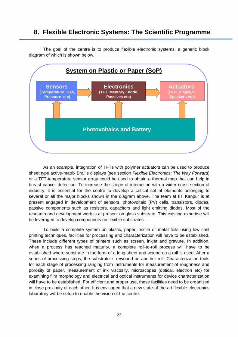
The goal of the centre is to produce flexible electronic systems, a generic block
diagram of which is shown below.
As an example, integration of TFTs with polymer actuators can be used to produce
sheet type active-matrix Braille displays (see section Flexible Electronics: The Way Forward)
or a TFT-temperature sensor array could be used to obtain a thermal map that can help in
breast cancer detection. To increase the scope of interaction with a wider cross-section of
industry, it is essential for the centre to develop a critical set of elements belonging to
several or all the major blocks shown in the diagram above. The team at IIT Kanpur is at
present engaged in development of sensors, photovoltaic (PV) cells, transistors, diodes,
passive components such as resistors, capacitors and light emitting diodes. Most of the
research and development work is at present on glass substrate. This existing expertise will
be leveraged to develop components on flexible substrates.
To build a complete system on plastic, paper, textile or metal foils using low cost
printing techniques, facilities for processing and characterization will have to be established.
These include different types of printers such as screen, inkjet and gravure. In addition,
when a process has reached maturity, a complete roll-to-roll process will have to be
established where substrate in the form of a long sheet and wound on a roll is used. After a
series of processing steps, the substrate is rewound on another roll. Characterization tools
for each stage of processing ranging from instruments for measurement of roughness and
porosity of paper, measurement of ink viscosity, microscopes (optical, electron etc) for
examining film morphology and electrical and optical instruments for device characterization
will have to be established. For efficient and proper use, these facilities need to be organized
in close proximity of each other. It is envisaged that a new state-of-the-art flexible electronics
laboratory will be setup to enable the vision of the centre.
24
Systems Integration Group
FlexE Team
Equipment
Support/
Development
Group
Device Development
Group
Electronics
Prototyping
Group
Materials
Group
IndustryPersonnel
FlexE Team
AcademicPersonnel
Prototyping
Invention
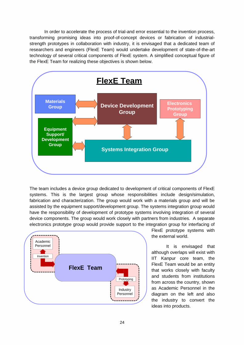
In order to accelerate the process of trial-and error essential to the invention process,
transforming promising ideas into proof-of-concept devices or fabrication of industrial-
strength prototypes in collaboration with industry, it is envisaged that a dedicated team of
researchers and engineers (FlexE Team) would undertake development of state-of-the-art
technology of several critical components of FlexE system. A simplified conceptual figure of
the FlexE Team for realizing these objectives is shown below.
The team includes a device group dedicated to development of critical components of FlexE
systems. This is the largest group whose responsibilities include design/simulation,
fabrication and characterization. The group would work with a materials group and will be
assisted by the equipment support/development group. The systems integration group would
have the responsibility of development of prototype systems involving integration of several
device components. The group would work closely with partners from industries. A separate
electronics prototype group would provide support to the integration group for interfacing of
FlexE prototype systems with
the external world.
It is envisaged that
although overlaps will exist with
IIT Kanpur core team, the
FlexE Team would be an entity
that works closely with faculty
and students from institutions
from across the country, shown
as Academic Personnel in the
diagram on the left and also
the industry to convert the
ideas into products.

25
The Ph.D. and M.Tech. thesis work will be the engine for generation of new ideas.
The FlexE Team will not only provide help in this process but also ensure that knowledge
generated is not lost with the graduation of the student, rather the knowledge is incorporated
in the technological products. The FlexE Team will also suggest topics where research and
innovation is required and these problems will be addressed in thesis work. This will help to
ensure that technology offered by the centre is unique and based on a portfolio of intellectual
property developed in-house. As indicated in the figure above, the FlexE Team will work
closely with personnel from industry, some of whom would be an integral part of it. The goal
here will be harness the knowledge base of the centre to develop industrial-strength
prototypes.
A major challenge in the whole endeavour is to recruit and retain high quality
manpower so that the centre becomes an incubation centre for domestic industry in FlexE
applications.
26
NAC (constituted in consultation with DeitY)
• Guides the Centre • Gives technology directions • Makes policies for the Centre • Approves collaborations with
academia and industry • Reviews the Centre performance
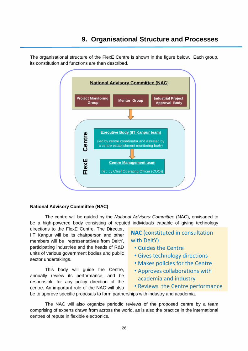
9. Organisational Structure and Processes
The organisational structure of the FlexE Centre is shown in the figure below. Each group,
its constitution and functions are then described.
National Advisory Committee (NAC)
The centre will be guided by the National Advisory Committee (NAC), envisaged to
be a high-powered body consisting of reputed individuals capable of giving technology
directions to the FlexE Centre. The Director,
IIT Kanpur will be its chairperson and other
members will be representatives from DeitY,
participating industries and the heads of R&D
units of various government bodies and public
sector undertakings.
This body will guide the Centre,
annually review its performance, and be
responsible for any policy direction of the
centre. An important role of the NAC will also
be to approve specific proposals to form partnerships with industry and academia.
The NAC will also organize periodic reviews of the proposed centre by a team
comprising of experts drawn from across the world, as is also the practice in the international
centres of repute in flexible electronics.
Fle
xE
Ce
ntr
e
Mentor GroupIndustrial Project
Approval Body
Executive Body (IIT Kanpur team)
(led by centre coordinator and assisted by
a centre establishment monitoring body)
National Advisory Committee (NAC)
Centre Management team
(led by Chief Operating Officer (COO))
Project Monitoring
Group
27
Mentor Group
• Advise Executive Body and NAC • Help develop national and
international networks
Projects Monitoring Group
• Conduct detailed project reviews • Approve changes to the proposal
within approved budget
In addition, to expedite decision making, the NAC would perform its functions through
the following smaller sub-groups: Mentor Group – 4 to 5 member scientific/technical group,
Projects Monitoring Group – a subset of the NAC and Industrial Projects Approval Body – a
group formed in consultation with DeitY for approving industrial projects. Each is described
further.
Mentor Group
This will be a group of 4-5 eminent
members, drawn both from academia and
industry. The constitution of this group
may be done on the advice of the
Executive Body. Although, the chair of the
mentor group will be an NAC member, the
body may have members outside of NAC
as well. The role of the Mentor Group will
be to advise the Executive Body on its strategic direction and help in developing a national
and international network both in academia and industry.
Projects Monitoring Group
Although, the overall performance of the centre will be reviewed by NAC annually, a detailed
project by project review is also necessary. It is envisaged that a smaller sub-group of NAC
will conduct these detailed reviews and provide feedback to NAC. It is important for the
success of the centre that it should be nimble enough in its approach so that as new
developments take place, new academic partners join in or specific partnerships with
industry are approved, appropriate timely changes in approach can be made. For example,
changes may be required in
altering the specifications of the
equipment as new or higher priority
needs are discovered. These
changes proposed by the Executive
Body may be approved by Projects
Monitoring Group which will have
the authority to take decisions as long as they are within the approved budget.
Industry Projects Approval Body

28
Executive Body (the Team at IIT Kanpur)
• Executes the functions of the centre • Prepares policies for engagement
with academic and industry ecosystem
• Responsible for the scientific programme at the centre
• Identifies industry partners and executes projects with them
• Coordinate development of roadmap for flexible electronics
Industry Projects Approval Body
• Evaluates and approves joint projects proposals from industry
• Manages Prototype Development Funds
An important feature of activities of the centre is to engage the industry in a
meaningful way that leads to manufacturing in the country. It is envisaged that at the time of
approval of the proposed
centre, a few participating
industries will be identified and
an expression of interest will
be sought from them. We
propose that a fraction of the
total project funds be reserved (as Prototype Development Fund) to finance these proposals.
The processes used to sanction these joint proposals will be kept the same as that followed
by DeitY. Thus, an Industry Projects Approval Body will be established. This body will be
responsible for sanction of the projects against the Prototype Development Fund. A subset
of NAC, the Projects Monitoring Group, as mentioned before, will perform the project
monitoring function. The financial audit at the time of sanction of the project will be
performed by Audit Department of IIT Kanpur.
This proposed mechanism is expected to ensure speedy approval of projects, with
same due diligence as practiced in DeitY. Further, by reserving a fund for projects leading to
product development, we may be able to leverage it for obtaining matching grants from
elsewhere.
Executive Body
The responsibility of project execution and management of the centre will lie with IIT
Kanpur through the team of faculty members at the Samtel Centre for Display Technologies,
IIT Kanpur. The Chief Operating Officer (COO) of the centre will be a part of this core team.
The coordinator of the Samtel Centre for Display Technologies, IIT Kanpur, appointed by the
Director of the institute, will be the ex-officio coordinator of the FlexE Centre. The COO and
other staff of the Centre will report to the Coordinator.
The role of this body will be to execute mandates of the centre as approved by the
NAC, which includes the following:
establish the centre
make policies for day to day
functioning of the centre and be
responsible to execute them
hire project manpower for the
centre, as per prior approval,
through IIT Kanpur processes
execute the scientific programme
of the centre, as per the approved
projects
29
prepare policy documents for engagement with academic ecosystem
prepare policy documents for engagement with Industrial ecosystem
identify industry partners and execute projects with them, with the intent for
manufacturing in future
Coordinate development of roadmap for flexible electronics
Centre Establishment Monitoring Body
This is a subset of the Executive Team having 2-3 persons. This structure is created
only for the first phase when substantial infrastructure development will be required. The
role of this sub-group will be to vigorously drive the time-lines for the establishment of the
centre.
Processes
Engagement within Academic Ecosystem
The Executive Body will identify international collaborators and establish MOUs with
them, after approval from the NAC. The object of this collaboration will be to accelerate
project execution and sharpen project objectives by identifying partners with complementary
strengths. The mechanism of interaction will include joint workshops and exchange of
research students.
A similar arrangement will be sought with partners within the country. However, the
centre will also provide Research Support to individuals in the country for a limited period.
The decision making for this activity will remain with the Executive Body.
Engagement with Industry Ecosystem
The interaction with the industry will also be through MOUs.
To deepen the engagement with the industry, the MOUs will provide for deployment
of their manpower at the centre for execution of specific projects and also for joint activities
in the centre. Their status in IIT Kanpur will be the same as that of project staff that works in
the IIT. This will allow access to the institute’s central facilities
An important feature will be encouragement to participating employees of the
industry to obtain post graduate degrees with the research performed at the centre, provided
the candidates fulfill the admission criteria and the other graduating requirements.
Levels of Engagements with Industry
Specific means for engagement with the industry will be evolved by the NAC. At this
point we are making one such suggestion which is given below.

30
Centre Partners will pay a fee determined by the NAC for establishing a partnership
with the centre. The Partner will be able to jointly write projects with IIT Kanpur team
members and apply for funding. Part of the financial requirement, will be contributed by the
industry. The Partners will be able to post personnel at IIT Kanpur and jointly share IP
developed in relation to the project executed with them.
Observer status will be granted by the NAC by paying a predetermined fee, lower
than that for a partner, under a MOU. The Observers will be able to place their personnel at
IIT Kanpur to work on the ongoing works at the centre. However, the Observers will not be
able to submit their project proposals to access Prototype Development Fund. The
Observers will have no claim to IP.
Work Packages will be developed jointly by industry and the team at IIT Kanpur.
These will typically be short term projects, fully funded by the industry. The IP will be jointly
owned.
Role of MOUs
All engagements with bodies outside IIT Kanpur, except with respect to IP protection
and work packages will be through a MOU with IIT Kanpur. IP protection will be governed
with separate agreement and work packages will be executed within the framework already
in practice at IIT Kanpur.
IP Protection
Prior to partnership with academic or industry partners, the centre through IIT Kanpur
will enter in an IP protection agreement.

31
10. The Programme of Activities
The team at IIT Kanpur submitted to DeitY (GOI) a concept paper for initiating activities
in flexible electronics, with due justification also given in this document. Following that, a
workshop to consider the concept paper was organized on 15 March, 2013. The
recommendations of the workshop are attached as Annexure I. The proposal below has
been prepared taking these recommendations into account.
10.1 Research and Development
This section briefly describes different works that would be carried out at the proposed
centre. The work will be broadly divided into two parts, namely “research” and
“development” with the FlexE Team in the middle enabling research on one end and working
towards component and prototype development on the other.
In the following, we provide activities which are envisaged at the start. However, we
emphasize that the list provided is an indicator; the activities would be added and some
directions changed as new knowledge becomes available and industry and academic
partners come on board. The process of managing this change has already been elaborated
in the section on “Organizational Structure and Processes”.
10.1.1 Research
Active research would be a key part of the centre where the core team will establish a
research programme to further the frontiers in flexible electronics and also research activities
that would lead to development of a component library. Basic engineering oriented research
would be carried out at the centre by post graduate students leading to Ph.D. and M. Tech.
degrees in accordance with the vision of the centre. Though the outlook of the research
would be futuristic, the FlexE Team would also suggest relevant research topics essential for
the development of components and prototypes. The research programme at the centre
would seek strategic collaboration with academic partners nationally and internationally to
augment existing research activities. Some of the research activities that would start in the
centre at its inception are enclosed as Annexure IIA. Details of initial collaborations for
research with Indian and foreign academic institutes and national laboratories are enclosed
as Annexure IIB. Increased collaborations would be the the outcome of roadmap
development workshops organised periodically. Annexures IIA and IIB only give a glimpse
of the kind of research activities that would start at this centre. These would evolve with the
centre, keeping the needs of industry in focus.
10.1.2 Development
Development of a component library with specifications tuned to product industry will be the
key task of the FlexE Team. This activity will be mentored by the core team with various
research inputs feeding into continuing development of the component library. The
specifications of the components will be decided in consultations with industry partners and
will be upgraded periodically. Development programme for some of the key enabling
components is enclosed as Annexure IIC. The specifications for components listed in
Annexure IIC are the initial targets that the FlexE Team strive to achieve. The target
specifications will be revised in light of the requirements of prototypes to be developed in

32
collaboration with industry partners. Besides component development, the FlexE Team will
also engage in prototype development with industry. The industry partners will be eligible to
write joint proposal for prototype development. These proposals will be reviewed and
approved by the “Industry Projects Approval Body” and, upon approval, these joint projects
will be able to utilize funds from “Prototype Development Funds” kept aside for this specific
purpose under PPP (Public-Private Partnership) model. The core team has been in
discussions with several industry partners and some of the application areas in which first
prototype development activity will start are outlined in Annexure IID.
Apart from enabling “Research” and “Development” activities as outlined above, the
centre would also engage in outreach activities. The key deliverables of the centre are
enumerated below. (Note: The deliverables of individual research and development activities
are provided separately)
10.2 Deliverables
1. Establish the infrastructure of the centre.
(A major activity in the initial years would be to develop the space for the centre,
develop arrangements for accommodation of participants and populate high-tech
equipment in the centre.)
2. Establish a research programme to engage in leading edge research in the area of
flexible electronics and build strategic academic collaborations.
3. Establish a research programme which leads to development of a critical set of
components suitable for rapid development of products.
(The proposed strategy is to build core competence in developing essential
components for a variety of applications, as elaborated in section “Flexible Electronic
(FlexE) Systems: The Scientific Programme.” Accordingly, the centre will identify
the device components, prepare their specifications and develop them in participation
with academic and research collaborators nationally and internationally. An effort
would also be made to involve the wider research community in this process.)
4. Develop prototypes in collaboration with industry for commercialization.
(As part of the recommendation of the workshop held to discuss the concept paper, it
was decided that the products that are to be developed at the centre should be
decided with the participating industry. As a strategy, we will select one that is
relatively easier to achieve and hence can be commercialized by the appropriate
industrial partner in a shorter period, and the other more challenging and thus likely
to take longer to commercialize.)
5. Coordinate development of national technology roadmap every three years for
flexible electronics.
(Workshops will be held together with persons in research and manufacturing for this
purpose; a national roadmap will be an outcome, relevant portions of which will be
followed by the centre. This activity will be a means of expanding national and
international academic.)

33
6. Establish standards for electronic products in the field of large area electronics.
(The centre will participate in strategic alliances globally, where these standards are
established.)
7. Coordinate outreach activities that lead to growth of R & D in flexible electronics by
conducting at least one workshop and a short course every year.
8. Create at least one spin-off commercial venture based on work done at the centre.
9. Generate human resource.
(Apart from graduating students with advanced degrees, the centre will also work
with industry participants to impart and upgrade relevant skills periodically. In the
duration of the project, we will produce at least 10 Ph.D.s and 20 M. Tech.s)
The next section discusses the budget, timelines and milestones.
34
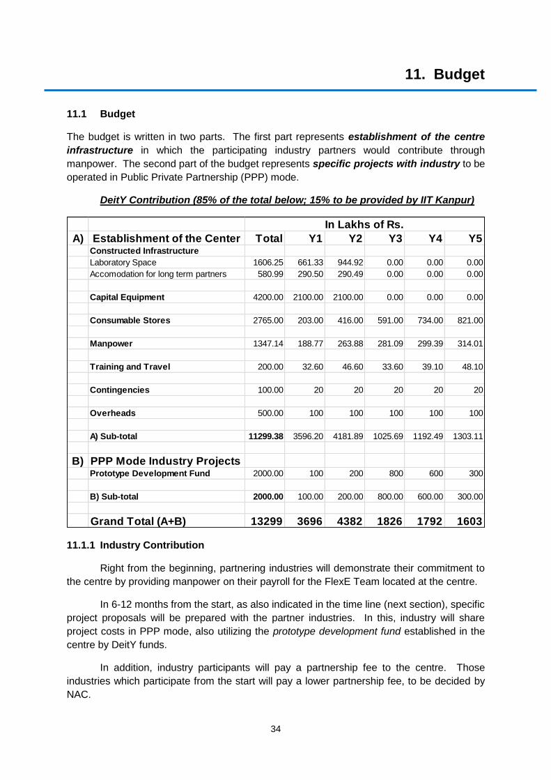
11. Budget
11.1 Budget
The budget is written in two parts. The first part represents establishment of the centre
infrastructure in which the participating industry partners would contribute through
manpower. The second part of the budget represents specific projects with industry to be
operated in Public Private Partnership (PPP) mode.
DeitY Contribution (85% of the total below; 15% to be provided by IIT Kanpur)
11.1.1 Industry Contribution
Right from the beginning, partnering industries will demonstrate their commitment to
the centre by providing manpower on their payroll for the FlexE Team located at the centre.
In 6-12 months from the start, as also indicated in the time line (next section), specific
project proposals will be prepared with the partner industries. In this, industry will share
project costs in PPP mode, also utilizing the prototype development fund established in the
centre by DeitY funds.
In addition, industry participants will pay a partnership fee to the centre. Those
industries which participate from the start will pay a lower partnership fee, to be decided by
NAC.
A) Establishment of the Center Total Y1 Y2 Y3 Y4 Y5Constructed Infrastructure
Laboratory Space 1606.25 661.33 944.92 0.00 0.00 0.00
Accomodation for long term partners 580.99 290.50 290.49 0.00 0.00 0.00
Capital Equipment 4200.00 2100.00 2100.00 0.00 0.00 0.00
Consumable Stores 2765.00 203.00 416.00 591.00 734.00 821.00
Manpower 1347.14 188.77 263.88 281.09 299.39 314.01
Training and Travel 200.00 32.60 46.60 33.60 39.10 48.10
Contingencies 100.00 20 20 20 20 20
Overheads 500.00 100 100 100 100 100
A) Sub-total 11299.38 3596.20 4181.89 1025.69 1192.49 1303.11
B) PPP Mode Industry ProjectsPrototype Development Fund 2000.00 100 200 800 600 300
B) Sub-total 2000.00 100.00 200.00 800.00 600.00 300.00
Grand Total (A+B) 13299 3696 4382 1826 1792 1603
In Lakhs of Rs.

35
11.1.2 IIT Kanpur Contribution
IIT Kanpur will contribute up to 15% of the total project cost towards constructed
infrastructure and manpower. Further, IIT Kanpur will provide support by way of (a) faculty
time, (b) use of its high-tech central laboratories, (c) workshop facilities and other
infrastructures, (d) utilities for the laboratories, (e) maintenance support of the civil
infrastructure and, (f) other support functions in form of project administration, purchases etc.
36
12. Potential Benefits to the Nation
With the successful establishment and functioning of this FlexE Centre, the nation should
derive various technological, scientific and strategic benefits that will also result in wide-
spread socio-economic benefits. The technological benefits will be in the form of expansion
of domestic manufacturing industry and ecosystem. These should not just lower the cost of
products and make them widely available, but will potentially benefit the rural and low
income sectors of India by providing opportunities for manpower and skill development and
job creation. In the following paragraphs, some of the key benefits are discussed.
1) Establish a nodal point for flexible electronics and create an ecosystem:
Flexible electronics is potentially going to change the way devices for various consumer
applications are perceived. However, establishing a lab to develop such devices requires
substantial financial support and infrastructure. Hence, there is a strong need to develop a
state-of-the-art laboratory at one strategic location which can serve as a nodal point for
brining India at par with the best in the world in this domain. Establishment of such a centre
at IIT Kanpur will allow smooth transition and conversion of ideas developed in localized
laboratories to actual devices and final product prototypes. The tangible benefits would be:
the centre would provide a platform to both academic world and industries to test their
ideas at the prototype level.
the Indian industry does not need to individually establish such a laboratory; that means
the centre serves as shared space for the Indian industry.
the infrastructure would allow the creation of a knowledge platform that would attract
international participation for contract R&D.
the centre would play a pivotal role in bringing together various industrial players
related to materials, equipments and devices thereby creating a much needed industrial
ecosystem for large area flexible electronics in India.
2) Place India on the world roadmap of flexible electronics:
Historically India has not been able to establish itself as a leading player in technological
product development. A timely setting-up of such a centre would help establish India as a
significant player in the emerging field of flexible electronics. This would be important both
from strategic as well as commercial point of view allowing significant savings in foreign
exchange, as technology would not need to be imported to establish a product line.
3) Device development and commercialisation:
One of the core aims of the centre is to develop devices that find use in practical
systems. The partnership model of academia and industry would help building proof of
concept devices and more importantly these flexible electronic devices are expected to
find application in commercially viable products. These devices would be as per the
requirements of products that are in tune with India’s need and do not have to be a sub-
optimal adoption or modification of device technology developed outside India.
37
It is planned that the FlexE Centre will spin-off at least one company which would have
the capability to commercially develop and manufacture devices based on flexible
electronics that cater to the needs within India.
4) IP creation:
The focus of effort on the up-coming large area flexible electronic technology should help in
the generation of core IP in the area. This is bound to have a wide range of benefits
including followings:
savings in foreign exchange and revenue, as many of these IP could be used as a cross-
licensing tool with foreign companies/institutes to obtain permission to use other patents
which might also be essential for the commercial manufacture of the final product.
revenue generation, as the IP generated at the centre can be potentially licensed to both
foreign as well as Indian companies (which won’t have to look outside India for these
licenses) working on this technology which can earn significant foreign exchange and
revenue for India.
5) Strategic product development:
Product development in this centre does need not be limited to commercial activities alone,
but may also be for strategic and social responsibility purposes. Very often, foreign sources
of know-how or products are not reliable or even viable. Some examples are given below.
Defence applications – special chemical sensors, light weight PV panels, etc.
Space applications - thin film solar cells for space vehicles, radiation hardened
electronics, etc. as many a times these technologies are not commercially available and
labs outside India may not transfer it to our forces for strategic/security reasons.
Rural applications – medical products for rural India that may not be sufficiently
commercially viable for foreign entities to take up research and development.
6) Human resource and skill development
One of the major issues which the manufacturing industries, specifically the high-tech
industries face in India, is the availability of trained manpower which can be productively
employed right away without significant costs associated with training them. The FlexE
Centre should alleviate this problem for the large area flexible electronic industry by:
generation of human resource as Ph.D.s and M.Tech.s from IIT Kanpur and other
partner academic institutions
organisation of regular workshops and seminars on industry and academic related topics
organisation specific workshops to address industry specific issues
joint programmes with industry where personnel get trained being part of the process.
7) Driving the technology as per India’s needs
The FlexE Centre will help establish country specific standards for electronic products in
the field of large area flexible electronics.
The FlexE Centre will coordinate the definition of national technology roadmap every
three years for flexible electronics with other stake holders. This will allow all the stake
holders including the government agencies and the associated industries to direct their
effort in a coherent and mutually beneficial manner. This is required for the country to be
able to take a leading global role in large area and flexible electronics technology.

38
13. Biographical Sketch of IITK Team
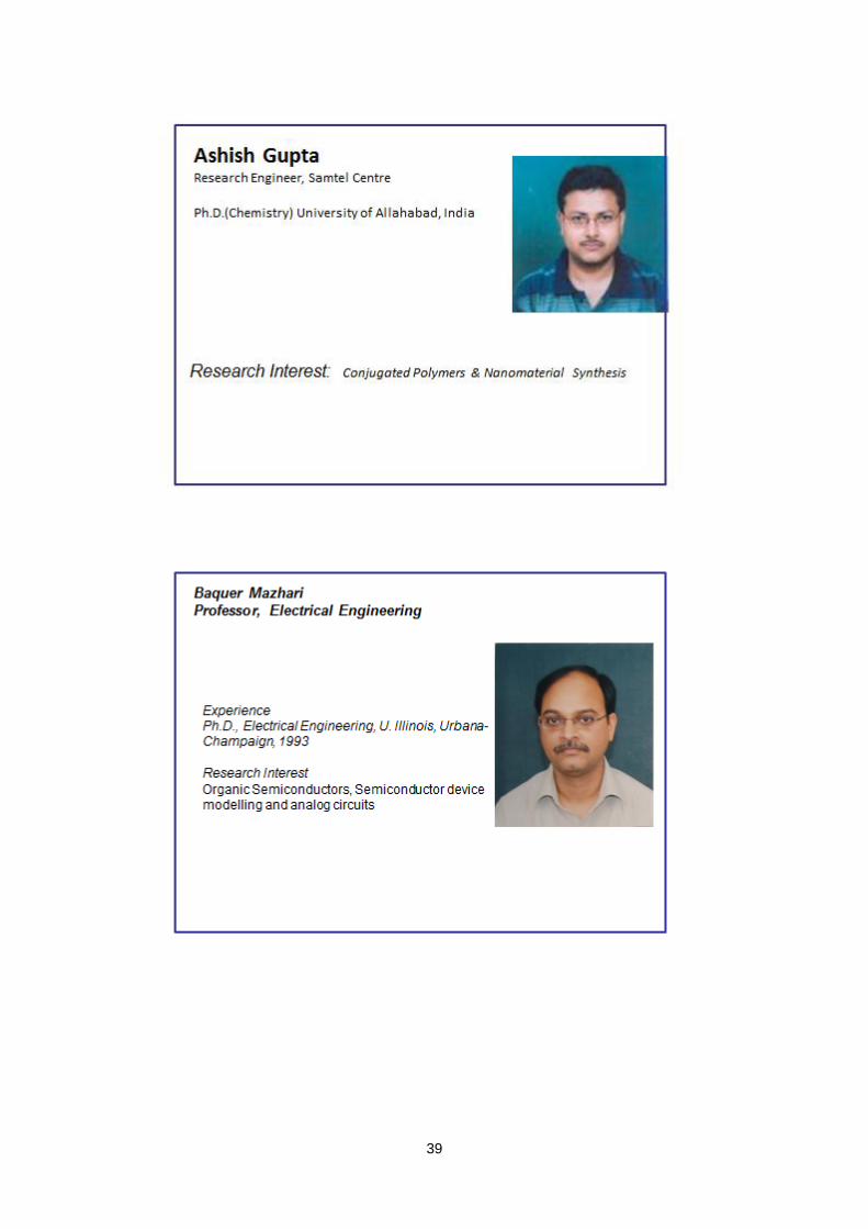
39
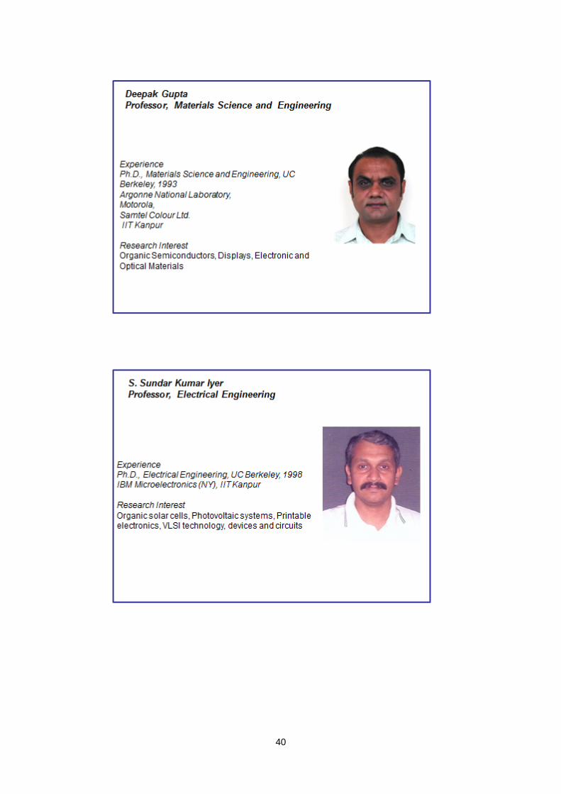
40
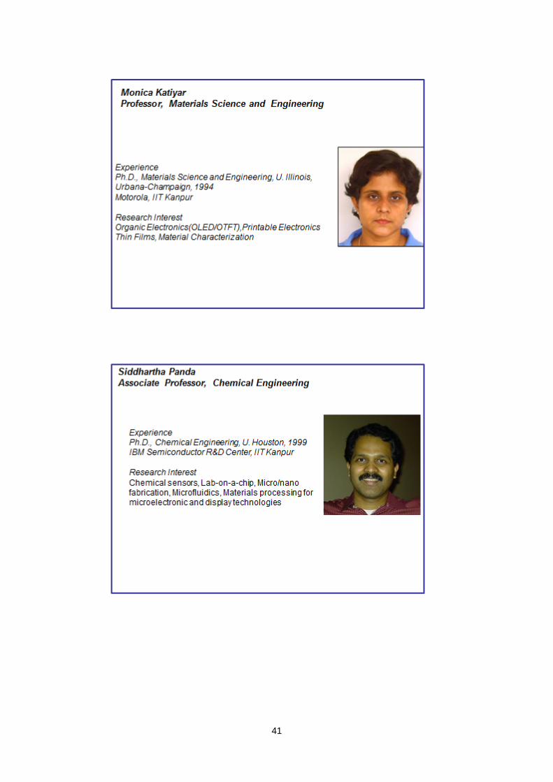
41
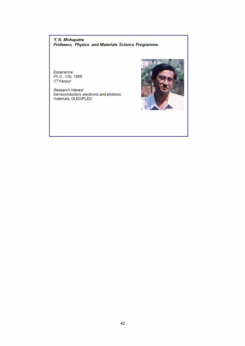
42

43
Annexure List
Annexure I: Minutes of the workshop on “Centre of Excellence for Large Area
Flexible Electronics” held at IIT Kanpur on March 15, 2013.
Annexure II: Programme of activities at the proposed centre
IIA: Research at the Centre
1. Development of carbon nanotubes and graphene based transparent electrodes
for flexible electronics
2. Design and Fabrication of an Organic Diode-based Temperature Sensor Array
3. Disease diagnostics from body fluids
4. Sensors for detection of heavy metals in water
5. Breathalyzer for non-invasive disease diagnostics
6. Development of environmentally stable and efficient organic solar cells
7. Self-assembled micron and nano-structures using solution processed materials
8. Development of a Compact Model for Organic Thin Film Transistor
9. Design and Fabrication of a Photodiode Sensor Array
10. Inorganic and Organic (IO) Hybrids for Flexible Memory and Smart Label
Display Applications
11. Synthesis and Formulation of Conductive Metal ink for Printed Electronics
IIB: Academic collaboration with academic/research labs in India and abroad
1. Flexible solid state Li- ion battery
2. Printable functional materials and devices
3. Lab-on-chip configuration for diabetic management
4. Collaboration on Printed Solar Cells on Paper
5. Organic, Hybrid and Polymeric Functional Materials for Flexible Electronics
IIC: Component development by FlexE Team at the Centre
1. Passive components for flexible electronics
2. Conducting polymer based temperature sensor array
3. Development of mini-modules of organic solar cells on substrates of sizes
150x150 mm2
4. Development of Thin Film Transistors for Diverse Range of Applications
5. White Organic Light-Emitting Diodes
6. Printed Organic Solar Cells on Paper
IID: Industrial partnership and prototype development
44
Annexure I: Minutes of the Workshop
45

46
47
48