cd stereo system model no. sa-akx10ph...
TRANSCRIPT

PSG1002034CE
CD Stereo System
Model No. SA-AKX10PHSA-AKX10PN
Product Color: (K)...Black Type
TABLE OF CONTENTSPAGE PAGE
1 Safety Precautions----------------------------------------------- 31.1. General Guidelines---------------------------------------- 31.2. Before Use (For PH only)-------------------------------- 31.3. Caution For Fuse Replacement------------------------ 31.4. Before Repair and Adjustment ------------------------- 41.5. Protection Circuitry ---------------------------------------- 41.6. Safety Parts Information --------------------------------- 4
2 Warning -------------------------------------------------------------- 62.1. Prevention of Electrostatic Discharge (ESD)
to Electrostatic Sensitive (ES) Devices -------------- 6
2.2. Precaution of Laser Diode -------------------------------72.3. Service caution based on Legal restrictions --------82.4. Handling Precautions for Traverse Unit --------------9
3 Service Navigation --------------------------------------------- 113.1. Service Information-------------------------------------- 11
4 Specifications ---------------------------------------------------- 125 Location of Controls and Components------------------ 13
5.1. Main Unit Key Button Operation---------------------- 135.2. Remote Control Key Button Operation ------------- 145.3. Media Information---------------------------------------- 15
Notes: This model’s CD Mechanism Unit is DLS6C. Please refer to the original service manual (Order No. MD0803034CE) for this mechanism
© Panasonic Corporation 2010. All rights reserved.Unauthorized copying and distribution is a violationof law.

6 Self-Diagnostic and Special Mode Setting ------------- 166.1. Cold-Start--------------------------------------------------- 166.2. Doctor Mode Table--------------------------------------- 176.3. Reliability Test Mode (CD Mechanism Unit
(DLS6C)) --------------------------------------------------- 196.4. Self-Diagnostic Mode ----------------------------------- 206.5. Self-Diagnostic Error Code Table -------------------- 21
7 Troubleshooting Guide---------------------------------------- 227.1. Troubleshooting Guide for F61 and/or F76 -------- 227.2. Part Location ---------------------------------------------- 237.3. D-Amp IC Operation & Control ----------------------- 26
8 Service Fixture & Tools --------------------------------------- 288.1. Service Tools and Equipment ------------------------- 28
9 Disassembly and Assembly Instructions --------------- 299.1. Disassembly Flow Chart-------------------------------- 309.2. Main Components and P.C.B. Locations ----------- 319.3. Disassembly of Top Cabinet--------------------------- 329.4. Disassembly of Tuner P.C.B.-------------------------- 339.5. Disassembly of Front Panel Assembly ------------- 339.6. Disassembly of Panel P.C.B. -------------------------- 359.7. Disassembly of Remote Sensor P.C.B.------------- 369.8. Disassembly of CD Open Button P.C.B.------------ 379.9. Disassembly of USB P.C.B. --------------------------- 37
9.10. Disassembly of CD Lid---------------------------------- 389.11. Disassembly of Main P.C.B. --------------------------- 399.12. Replacement of Regulator IC (IC2701)------------- 409.13. Disassembly of D-Amp P.C.B. ------------------------ 419.14. Replacement of Audio Digital Amp IC
(IC5900) ---------------------------------------------------- 439.15. Disassembly of SMPS P.C.B. ------------------------- 449.16. Replacement of Switching Regulator IC
(IC5701) ---------------------------------------------------- 469.17. Replacement of Rectifier Diode (D5702)----------- 479.18. Replacement of Regulator Diode (D5801)--------- 499.19. Replacement of Regulator Diode (D5802)--------- 509.20. Replacement of Regulator Diode (D5803)--------- 519.21. Disassembly of CD Mechanism Unit (DLS6C) --- 529.22. Disassembly of Rear Panel---------------------------- 549.23. Disassembly of Voltage Selector P.C.B. (For
PH only) ---------------------------------------------------- 559.24. Disassembly of CD Servo P.C.B.--------------------- 56
10 Replacement of Traverse Unit ------------------------------ 5810.1. Disassembling Procedures ---------------------------- 5810.2. Assembling Procedure---------------------------------- 59
11 Service Position ------------------------------------------------- 6111.1. Checking and Repairing of Main P.C.B. ------------ 6111.2. Checking and Repairing of D-Amp P.C.B. --------- 6111.3. Checking and Repairing of Panel P.C.B. ----------- 6111.4. Checking and Repairing of USB P.C.B. ------------ 6211.5. Checking and Repairing of SMPS P.C.B. ---------- 62
12 Voltage & Waveform Chart ----------------------------------- 6412.1. CD SERVO P.C.B. --------------------------------------- 6412.2. Main P.C.B. (1/2) ----------------------------------------- 6512.3. Main P.C.B. (2/2) ----------------------------------------- 6612.4. Panel P.C.B. ----------------------------------------------- 6612.5. USB P.C.B.------------------------------------------------- 6712.6. D-Amp P.C.B. --------------------------------------------- 6712.7. SMPS P.C.B. ---------------------------------------------- 6812.8. Tuner P.C.B. ----------------------------------------------- 6812.9. Waveform Table ------------------------------------------ 69
13 Illustration of ICs, Transistor and Diode ---------------- 70
14 Simplified Block Diagram------------------------------------ 7114.1. Overall Simplified Block Diagram-------------------- 7114.2. D-Amp Block Diagram---------------------------------- 72
15 Block Diagram --------------------------------------------------- 7315.1. Servo/System Control ---------------------------------- 7315.2. Audio-------------------------------------------------------- 7415.3. Power Amplifier ------------------------------------------ 7515.4. Power Supply--------------------------------------------- 76
16 Wiring Diagram-------------------------------------------------- 7717 Schematic Diagram Notes ----------------------------------- 7918 Schematic Diagram -------------------------------------------- 81
18.1. CD Servo Circuit ----------------------------------------- 8118.2. Main Circuit------------------------------------------------ 8218.3. Panel Circuit ---------------------------------------------- 8618.4. CD Open Button, Remote Sensor & Tuner
Circuit ------------------------------------------------------- 8718.5. USB Circuit ------------------------------------------------ 8818.6. D-Amp Circuit--------------------------------------------- 8918.7. SMPS Circuit---------------------------------------------- 9018.8. Voltage Selector Circuit (For PH Only) ------------- 92
19 Printed Circuit Board------------------------------------------ 9319.1. CD Servo, Tuner & Voltage Selector P.C.B. ------ 9319.2. Main P.C.B.------------------------------------------------ 9419.3. Panel P.C.B.----------------------------------------------- 9519.4. CD Open Button, Remote Sensor, USB & D-
Amp P.C.B. ------------------------------------------------ 9619.5. SMPS P.C.B. (For PH only) --------------------------- 9719.6. SMPS P.C.B. (For PN only) --------------------------- 98
20 Terminal Function of ICs ------------------------------------- 9920.1. IC2801 (RFKWMAKX10PN): IC MICRO-
PROCESSOR -------------------------------------------- 9920.2. IC6901(C0HBB0000057): IC FL Driver ------------ 99
21 Exploded View and Replacement Parts List----------10121.1. Exploded View and Mechanical replacement
Part List ---------------------------------------------------10121.2. Electrical Replacement Part List --------------------107
2

1 Safety Precautions1.1. General Guidelines
1. When servicing, observe the original lead dress. If a short circuit is found, replace all parts which have been overheated ordamaged by the short circuit.
2. After servicing, see to it that all the protective devices such as insulation barriers, insulation papers shields are properlyinstalled.
3. After servicing, carry out the following leakage current checks to prevent the customer from being exposed to shock hazards.
1.1.1. LEAKAGE CURRENT COLD CHECK1. Unplug the AC cord and connect a jumper between the two prongs on the plug.2. Measure the resistance value, with an ohmmeter, between the jumpered AC plug and each exposed metallic cabinet part on
the equipment such as screwheads, connectors, control shafts, etc. When the exposed metallic part has a return path to thechassis, the reading should be between 1MΩ and 5.2MΩ.When the exposed metal does not have a return path to the chassis, the reading must be
1.1.2. LEAKAGE CURRENT HOT CHECK1. Plug the AC cord directly into the AC outlet. Do not use an isolation transformer for this check.2. Connect a 1.5kΩ, 10 watts resistor, in parallel with a 0.15µF capacitors, between each exposed metallic part on the set and a
good earth ground such as a water pipe, as shown in Figure 1.3. Use an AC voltmeter, with 1000 ohms/volt or more sensitivity, to measure the potential across the resistor.4. Check each exposed metallic part, and measure the voltage at each point.5. Reverse the AC plug in the AC outlet and repeat each of the above measurements.6. The potential at any point should not exceed 0.75 volts RMS. A leakage current tester (Simpson Model 229 or equivalent)
may be used to make the hot checks, leakage current must not exceed 1/2 milliamp. In case a measurement is outside of thelimits specified, there is a possibility of a shock hazard, and the equipment should be repaired and rechecked before it isreturned to the customer.
Figure 1
1.2. Before Use (For PH only)Be sure to disconnect the mains cord before adjusting the voltage selector.Use a minus(-) screwdriver to set the voltage selector (on the rear panel) to the voltage setting for the area in which the unit will beused. (If the power supply in your area is 110V ~ 127V or 220V ~ 240V, set to the “110V ~ 127V or 220V ~ 240V” position.)Note that this unit will be seriously damaged if this setting is not made correctly. (There is no voltage selector for some countries,the correct voltage is already set.)
1.3. Caution For Fuse Replacement
3

1.4. Before Repair and AdjustmentDisconnect AC power to discharge unit AC Capacitors as such (C5701, C5703, C5704, C5705, C5706, C5707, C5708) through a10 Ω, 10 W resistor to ground.Caution:
DO NOT SHORT-CIRCUIT DIRECTLY (with a screwdriver blade, for instance), as this may destroy solid state devices.After repairs are completed, restore power gradually using a variac, to avoid overcurrent.Current consumption at AC 120 V, 60 Hz in NO SIGNAL mode volume minimal should be ~ 500 mA. (PN)
Current consumption at AC 110~127 V / 220~240 V, 50/60 Hz in NO SIGNAL mode volume minimal should be ~ 500 mA. (PH)
1.5. Protection CircuitryThe protection circuitry may have operated if either of the following conditions are noticed:
• No sound is heard when the power is turned on.• Sound stops during a performance.
The function of this circuitry is to prevent circuitry damage if, for example, the positive and negative speaker connection wires are“shorted”, or if speaker systems with an impedance less than the indicated rated impedance of the amplifier are used.If this occurs, follow the procedure outlines below:
1. Turn off the power.2. Determine the cause of the problem and correct it.3. Turn on the power once again after one minute.
Note:When the protection circuitry functions, the unit will not operate unless the power is first turned off and then on again.
1.6. Safety Parts InformationSafety Parts List:
There are special components used in this equipment which are important for safety.
These parts are marked by in the Schematic Diagrams & Replacement Parts List. It is essential that these critical partsshould be replaced with manufacturer’s specified parts to prevent shock, fire or other hazards. Do not modify the original designwithout permission of manufacturer.
Safety Ref. No. Part No. Part Name & Description Remarks
6 REXX1030 1P RED WIRE (VOLTAGE-SMPS) PH
7 REXX1031 1P BLACK WIRE (VOLTAGE-SMPS) PH
13 RGRX1002A-A2 REAR PANEL PN
13 RGRX1002B-A2 REAR PANEL PH
37 RKMX1003-K TOP CABINET
401 RAEX0190Z-V TRAVERSE UNIT
A2 K2CB2CB00021 AC CORD PN
A2 K2CQ2CA00007 AC CORD PH
A3 RQTX1084-M O/I BOOK (En,SP)
A3 RQTX1085-M O/I BOOK (Sp) PH
A6 K2DAYYY00002 AC PLUG ADAPTER PH
PCB3 REPX0809A SMPS P.C.B. (RTL) PN
PCB3 REPX0809C SMPS P.C.B. (RTL) PH
PCB10 REPX0809C VOLTAGE SELECTOR P.C.B. (RTL) PH
DZ5701 ERZV10V511CS ZNR
S5701 K0ABCA000007 SW VOLTAGE SELECTOR PH
L5703 G0B612H00002 LINE FILTER
T5701 ETS39AG4M6AD MAIN TRANSFORMER PH
T5701 ETS39AG4NGAD MAIN TRANSFORMER PN
T5751 ETS19AB2E6AG SUB TRANSFORMER
T6101 G4DYA0000214 SWITCHING TRANSFORMER
PC5701 B3PBA0000402 PHOTO COUPLER
PC5702 B3PBA0000402 PHOTO COUPLER
PC5720 B3PBA0000402 PHOTO COUPLER
PC5799 B3PBA0000402 PHOTO COUPLER
F1 K5D632BK0007 FUSE PH
F1 K5D802APA008 FUSE PN
TH5702 D4CAA2R20001 THERMISTOR
TH5860 D4CC11040013 THERMISTOR
TH5900 D4CC11040013 THERMISTOR
P5701 K2AA2B000011 AC INLET PH
P5701 K2AB2B000007 AC INLET PN
C5701 F0CAF334A105 0.33uF
C5703 F0CAF104A105 0.1uF PH
4

C5703 F0CAF224A105 0.22uF PN
C5704 F1BAF1020020 1000pF
C5705 F1BAF1020020 1000pF
C5706 F1BAF1020020 1000pF PH
C5707 F1BAF1020020 1000pF PH
C5708 F1BAF1020020 1000pF
Safety Ref. No. Part No. Part Name & Description Remarks
5

2 Warning2.1. Prevention of Electrostatic Discharge (ESD) to Electrostatic Sensitive
(ES) DevicesSome semiconductor (solid state) devices can be damaged easily by static electricity. Such components commonly are called Elec-trostatically Sensitive (ES) Devices. Examples of typical ES devices are integrated circuits and some field-effect transistors andsemiconductor "chip" components. The following techniques should be used to help reduce the incidence of component damagecaused by electrostatic discharge (ESD).
1. Immediately before handling any semiconductor component or semiconductor-equipped assembly, drain off any ESD on yourbody by touching a known earth ground. Alternatively, obtain and wear a commercially available discharging ESD wrist strap,which should be removed for potential shock reasons prior to applying power to the unit under test.
2. After removing an electrical assembly equipped with ES devices, place the assembly on a conductive surface such as alumi-num foil, to prevent electrostatic charge buildup or exposure of the assembly.
3. Use only a grounded-tip soldering iron to solder or unsolder ES devices.4. Use only an anti-static solder removal device. Some solder removal devices not classified as “anti-static (ESD protected)” can
generate electrical charge sufficient to damage ES devices.5. Do not use freon-propelled chemicals. These can generate electrical charges sufficient to damage ES devices.6. Do not remove a replacement ES device from its protective package until immediately before you are ready to install it. (Most
replacement ES devices are packaged with leads electrically shorted together by conductive foam, aluminum foil or compara-ble conductive material).
7. Immediately before removing the protective material from the leads of a replacement ES device, touch the protective materialto the chassis or circuit assembly into which the device will be installed.Caution:
Be sure no power is applied to the chassis or circuit, and observe all other safety precautions.8. Minimize bodily motions when handling unpackaged replacement ES devices. (Otherwise harmless motion such as the
brushing together of your clothes fabric or the lifting of your foot from a carpeted floor can generate static electricity (ESD) suf-
ficient to damage an ES device).
6

2.2. Precaution of Laser Diode
Caution:This product utilizes a laser diode with the unit turned “on”, invisible laser radiation is emitted from the pickup lens.Wavelength: 785 nm (CD)Maximum output radiation power from pickup: 100 µW/VDELaser radiation from the pickup unit is safety level, but be sure the followings: 1. Do not disassemble the pickup unit, since radiation from exposed laser diode is dangerous. 2. Do not adjust the variable resistor on the pickup unit. It was already adjusted.3. Do not look at the focus lens using optical instruments.4. Recommend not to look at pickup lens for a long time.
7

2.3. Service caution based on Legal restrictions
2.3.1. General description about Lead Free Solder (PbF)The lead free solder has been used in the mounting process of all electrical components on the printed circuit boards used for thisequipment in considering the globally environmental conservation.
The normal solder is the alloy of tin (Sn) and lead (Pb). On the other hand, the lead free solder is the alloy mainly consists of tin(Sn), silver (Ag) and Copper (Cu), and the melting point of the lead free solder is higher approx.30 degrees C (86°F) more than thatof the normal solder.
Definition of PCB Lead Free Solder being used
Service caution for repair work using Lead Free Solder (PbF)• The lead free solder has to be used when repairing the equipment for which the lead free solder is used.
(Definition: The letter of “PbF” is printed on the PCB using the lead free solder.)• To put lead free solder, it should be well molten and mixed with the original lead free solder.• Remove the remaining lead free solder on the PCB cleanly for soldering of the new IC.• Since the melting point of the lead free solder is higher than that of the normal lead solder, it takes the longer time to melt the
lead free solder.• Use the soldering iron (more than 70W) equipped with the temperature control after setting the temperature at 350±30 degrees
C (662±86°F).Recommended Lead Free Solder (Service Parts Route.)
• The following 3 types of lead free solder are available through the service parts route.RFKZ03D01K-----------(0.3mm 100g Reel)RFKZ06D01K-----------(0.6mm 100g Reel)RFKZ10D01K-----------(1.0mm 100g Reel)
Note* Ingredient: tin (Sn), 96.5%, silver (Ag) 3.0%, Copper (Cu) 0.5%, Cobalt (Co) / Germanium (Ge) 0.1 to 0.3%
The letter of “PbF” is printed either foil side or components side on the PCB using the lead free solder. (See right figure)
8

2.4. Handling Precautions for Traverse UnitThe laser diode in the optical pickup unit may break down due to static electricity of clothes or human body. Special care must betaken avoid caution to electrostatic breakdown when servicing and handling the laser diode in the traverse unit.
2.4.1. Cautions to Be Taken in Handling the Optical Pickup UnitThe laser diode in the optical pickup unit may be damaged due to electrostatic discharge generating from clothes or human body.Special care must be taken avoid caution to electrostatic discharge damage when servicing the laser diode.
1. Do not give a considerable shock to the optical pickup unit as it has an extremely high-precise structure.2. To prevent the laser diode from the electrostatic discharge damage, the flexible cable of the optical pickup unit removed
should be short-circuited with a short pin or a clip.3. The flexible cable may be cut off if an excessive force is applied to it. Use caution when handling the flexible cable.4. The antistatic FPC is connected to the new optical pickup unit. After replacing the optical pickup unit and connecting the flexi-
ble cable, cut off the antistatic FPC.
2.4.2. Grounding for electrostatic breakdown preventionSome devices such as the DVD player use the optical pickup (laser diode) and the optical pickup will be damaged by static electric-ity in the working environment. Proceed servicing works under the working environment where grounding works is completed.
2.4.2.1. Worktable grounding1. Put a conductive material (sheet) or iron sheet on the area where the optical pickup is placed, and ground the sheet.
9

2.4.2.2. Human body grounding1. Use the anti-static wrist strap to discharge the static electricity form your body.
10
3 Service Navigation3.1. Service InformationThis service manual contains technical information which will allow service personnel’s to understand and service this model.Please place orders using the parts list and not the drawing reference numbers.
If the circuit is changed or modified, this information will be followed by supplement service manual to be filed with original servicemanual.
• CD Mechanism unit (DLS6C):
1) This model uses CD Mechanism Unit (DLS6C).
2) This service manual does not contain the following information on CD Mechanism Unit (DLS6C) - Schematic Diagram, Block Diagram and P.C.B. layout of CD Mechanism Unit (DLS6C) P.C.B. - Parts List for individual parts of CD Mechanism Unit (DLS6C). - Exploded View and Part List for individual parts of CD Mechanism Unit (DLS6C). Please refer to original service manual (Order No. MD0803034CE)
• Micro-processor:
1) The following components are supplied as an assembled part. - Micro-processor IC, IC2801 (RFKWMAKX10PN)
• Speaker system:
1) This model uses speaker, SB-AKX10PN-K (PSG1001001CE)
11

4 Specifications
AMPLIFIER SECTIONRMS output power stereo mode
Front Ch (both channels driven)125 W per channel (4 Ω), 1 kHz, 10% THD
Total RMS stereo mode power250 W
PMPO output power (PN only)2800 W
FM/AM TUNER, TERMINALS SECTIONPreset station FM 30 stations AM 15 stationsFrequency Modulation (FM)
Frequency rangeFor PH only
87.50 to 108.00 MHz (50 kHz step)For PN only
87.9 to 107.9 MHz (200 kHz step)87.5 to 108.0 MHz (100 kHz step)
Antenna terminal (s)75 Ω (unbalanced)
Amplitude Modulation (AM)Frequency rangeFor PH only
522 to 1629 kHz (9 kHz step)520 to 1630 kHz (10 kHz step)
For PN only520 to 1710 kHz (10 kHz step)
AUX InputRCA pin jack
DISC SECTIONDiscs played (8 cm or 12 cm)(1) CD-Audio (CD-DA)(2) CD-R/RW (CD-DA, MP3* formatted disc)(3) MP3** MPEG-1 layer 3Pick up
Wavelength 785 nm(CD)Laser Power CLASS 1 (CD)
Audio output (Disc)Number of channels 2 (FL, FR)FL = Front left channelFR = Front right channel
USB SECTIONUSB Port
USB standard USB 2.0 full speedMedia file format support MP3 (*.mp3)USB device file system FAT12, FAT16, FAT32USB Port power 500 mA (max)
GENERALPower supplyFor PH only
AC 110 to 127 V, 50 HzAC 220 to 240 V, 60 Hz
For PN onlyAC 120 V, 60 Hz
Power ConsumptionFor PH only
64 WFor PN only
61 WDimensions (W x H x D) 250 mm x 336 mm x 245 mmMass 3 kgOperating temperature range 0 °C to +40 °COperating humidity range 35% to 80% RH
(no condensation)
Power Consumption in standby modeFor PH only 0.3 W (Approximate)For PN only 0.2 W (Approximate)
Notes1. Specifications are subject to change without notice.
Mass and dimensions are approximate.2. Total harmonic distortion is measured by the digital spectrum
analyzer. System: SC-AKX10PN-K
Main Unit: SA-AKX10PN-KFront Speakers: SB-AKX10PN-K
System: SC-AKX10PH-KMain Unit: SA-AKX10PH-K
Front Speakers: SB-AKX10PN-K
12

5 Location of Controls and Components5.1. Main Unit Key Button Operation
USB/
AUX
POWER
VOLUME +
OPEN CLOSE
MANUAL EQ
ALBUM
FM/AM
TRACKCD
/
/
/
17
[MANUAL EQ] selection
Remote control signal sensor
USB play or pause
[USB, / ]
Stop function
[ ]
USB port
D.BASS Selection
[AUX]
Volume Control
Press to switch the unit from on to standby mode or vice versa.
In standby mode, the unit is still consuming a small amount of
power.
Standby/on switch ( /l, POWER)
Display Panel
Disc tray open or close
[ , OPEN/CLOSE]
Tuner (FM/AM) Selection
[Track]
Skip and play your desired track
Disc play and pause
[ CD, / ]
Album selection
Track skip or search,
fast-forward or rewind,
tune or preset channel selection,
sound quality adjustment,
manual EQ setting (BASS & TREBLE)
[ / ][ / ]
Disc tray17
13

5.2. Remote Control Key Button Operation
14

5.3. Media Information
15

6 Self-Diagnostic and Special Mode Setting6.1. Cold-StartHere is the procedure to carry out cold-start or initialize to shipping mode.
1. Unplug AC power cord2. Press & hold [POWER] button3. Plug AC power cord while [POWER] button being pressed
FL Display will show “_ _ _ _ _ _ _ _”4. Release [POWER] button
16
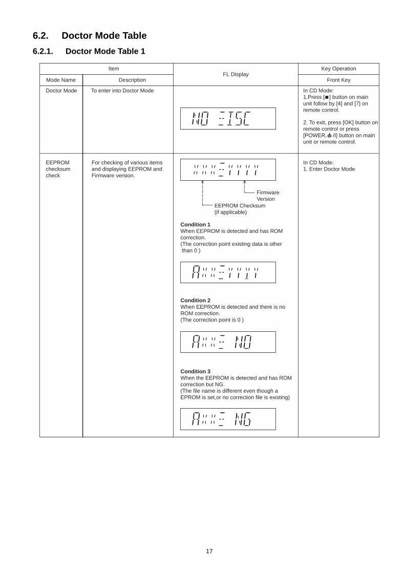
6.2. Doctor Mode Table
6.2.1. Doctor Mode Table 1
FL DisplayKey Operation
Front Key
Item
DescriptionMode Name
Doctor Mode
EEPROM
checksum
check
Firmware
Version
EEPROM Checksum
(if applicable)
To enter into Doctor Mode In CD Mode:
1.Press [ ] button on main
unit follow by [4] and [7] on
remote control.
2. To exit, press [OK] button on
remote control or press
[POWER, /I] button on main
unit or remote control.
Condition 1
When EEPROM is detected and has ROM
correction.
(The correction point existing data is other
than 0 )
Condition 2
When EEPROM is detected and there is no
ROM correction.
(The correction point is 0 )
Condition 3
When the EEPROM is detected and has ROM
correction but NG.
(The file name is different even though a
EPROM is set,or no correction file is existing)
For checking of various items
and displaying EEPROM and
Firmware version.
In CD Mode:
1. Enter Doctor Mode
17

6.2.2. Doctor Mode Table 2
FL DisplayKey Operation
Front Key
Item
DescriptionMode Name
Cold Start
Volume Setting
Check
FL Display
Check
To active cold start upon next AC
power up when reset start is execute
the next time.
To check the volume setting of a main
unit.
To check the FL segment display
All segment will light up while all LED
blink at 0.5s,intervals.(if any)
In Doctor Mode:
1. Press [4] button on
remote control.
In Doctor Mode:
1. Press [7],[8],[9],[>10]
button on remote control.
In Doctor mode:
1. Press [2] button on
remote control.
Press [7]: VOLUME50
Press [8]: VOLUME35
Press [9]: VOLUME27
Press [>10]: VOLUME0
Volume
In this mode, the tray will open & close.
Note: Refer to Section 6.3 Fig 1 for process flow.
The counter willincrement by one.When reach 9999will change to 0000
Cancellation Display
DLS6 ReliabilityTest (Loading)
To determine CD Mechanism Unit(DLS6C) Open/Close operation.
In Doctor Mode:1.Press [5] button on remote control.
2.To cancel, press [0] on remote control.
Note: Refer to Section 6.3 Fig 2. for process flow.
The counter willincrement by one.When reach 9999will change to 0000
Cancellation Display
DLS6 ReliabilityTest (Traverse)
To determine CD Mechanism DLS6CAccess Inner & Outer disc operation.
In Doctor Mode:1.Press [6] button on remote control.
2.To cancel, press [0] on remote control.
Note: Refer to Fig. 6.3. for processflow.
The counter willincrement by one.When reach 9999will change to 0000
Cancellation Display
DLS6 ReliabilityTest (Combination)
In Doctor Mode:1.Press [DIMMER] button on remote control.
2.To cancel, press [0] on remote control.
In this mode,ensure the CD is in the main unit.
To determine CD Mechanism Unit (DLS6C) Open/Close & Access Inner & Outer Disc Operation.
In this mode,ensure the CD is in the main unit.
18
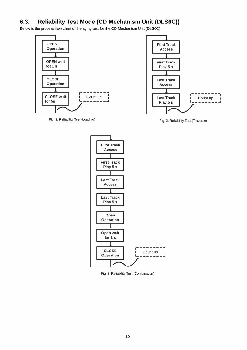
6.3. Reliability Test Mode (CD Mechanism Unit (DLS6C))Below is the process flow chart of the aging test for the CD Mechanism Unit (DLS6C).
Fig. 1. Reliability Test (Loading)
Fig. 2. Reliability Test (Traverse)
Fig. 3. Reliability Test (Combination)
OPEN
Operation
OPEN wait
fot 1 s
CLOSE
Operation
CLOSE wait
for 5sCount up
First Track
Access
First Track
Play 5 s
Last Track
Access
Last Track
Play 5 sCount up
First Track
Access
First Track
Play 5 s
Last Track
Access
Last Track
Play 5 s
Open
Operation
Open wait
for 1 s
CLOSE
OperationCount up
19

6.4. Self-Diagnostic Mode
FL DisplayKey Operation
Front Key
Item
DescriptionMode Name
To enter into self-diagnostic.Self-DiagnosticMode
To unlock the mechanism unit for service.
During the process,’’SRCV TRV’’ will blink.
When ready "SRVC TRV" will stop blinking.
In this mode, the disassembly of DLS6C can be carry out. (Refer to original service manual for CD Mechanism Unit (DLS6C))
Service Mode
In AUX Mode:1. Press and hold [STOP] button on the main unit for 2 secs.
2. Do not release [STOP] button, press & hold [ / ] on the main unit for 2 secs.
3. To exit, press [POWER, ] button on main unit.
/l
In Self-Diagnostic Mode:
1. Press [ Open / Close] button on main unit.
2.To exit,press [POWER ] button on main unit.
/l(Blinking)
(Display 1)
(Display 2)
20

6.5. Self-Diagnostic Error Code TableSelf-Diagnostic Function (Refer Section 6.4. Self-Diagnostic Mode) provides information on any problems occurring for the unit andits respective components by displaying the error codes. These error code such as U**, H** and F** are stored in memory and heldunless it is cleared.The error code is automatically display after entering into self-diagnostic mode.
6.5.1. Power Supply Error Code Table
6.5.2. Mechanism Error Code Table (CD Mechanism Unit (DLS6C))
Error Code Diagnosis Contents Description of error Automatic FL Display Remarks
F61 Power Amp IC outputabnormal
Upon power on,PCNT=HIGH, DCDET2=Lafter checking LSI.
Press [ ] on main unit fornext error.
F76 DCDET1 = L (NG)
F61-76 Both DCDET1 andDCDET2 L(NG)
-DEMO
Error Code Diagnosis Contents Description of error Automatic FL Display Remarks
F15 CD REST SW Abnormal Press [ ] on main
unit for next error.
F26 Communication between
CD servo LSI and micro-p
abnormal.
Press [ ] on main
unit for next error.
H15 CD Open SW Abnormal During normal operation
CD OPEN SW On fail to be
detected with 3 sec.
Press [ ] on main
unit for next error.
CD traverse position initial
setting operation fail safe
time is over (10 sec) waiting
for REST SW to turn on.
At the time of switching to
CD function,SENSE = H
shall be detected using
DTMS system setting
command. If the error is
memorized when SENSE
= L is not detected within
fail safe timer time (20ms),
[F26] shall be displayed
simultaneously.This
display shall be retained if
the power is ON and at
CD function. If this error
occurs, CD operation
afterwards shall not be
executed as in the case of
[NO DISC].
H16 CD closing SW abnormal During Closing operation,if
"POS_SW_CEN" is not
detected within 3 secs.
Press [ /-DEMO]on main
unit for next error.
21

7 Troubleshooting Guide7.1. Troubleshooting Guide for F61 and/or F76This section illustrates the checking procedures when upon detecting the error of “F61” and/or “F76” after power up of the unit. It isfor purpose of troubleshooting and checking in SMPS, D-Amp & Main P.C.B.
Symptom Remarks
Set cannot ON 1 AC Cord 1 AC Cord Faulty, Loose connection. Refer to
Section 7.2.1
Fig. 1. SMPS
P.C.B.
Refer to
Section 7.2.1
Fig. 1. SMPS
P.C.B.
Refer to
Section 7.2.2
Fig. 2. Main P.C.B.
Refer to
Section 7.2.1
Fig. 1. SMPS P.C.B.
Refer to
Section 7.2.1
Fig. 1. SMPS
P.C.B.
2 AC Inlet, P5701 2 P5701 solder crack, dry joint.
3 Fuse, F1 3 Fuse, F1 Open.
4 Photocoupler 4 PC5702/PC5799 solder crack.
PC5702, PC5799 Dry joint, short circuit, open circuit.
5 Switching IC, IC5701 5 IC5701 Faulty.
6 Switching IC, IC5799 6 IC5799 Faulty.
Set can ON 1 Speaker Output 1 Faulty speaker unit, Loose connection, Short. Refer to
Section 7.2.3
Fig. 3. D-Amp
P.C.B.
then F61
2 D-AMP circuit 2a D-AMP IC, IC5900 defective.
(DC voltage of +/-30V detected at speaker output)
Set can ON 1 Transformer T5701 1a Short circuit between Pin 14 and Pin 15.
then F76 1b Short circuit between Pin 15 and Pin 16.
1c Short circuit between Pin 16 and Pin 17.
2 DC-DC Circuit 2a Check cable wire connection between cable wire ZJ2701
(At Main P.C.B) & connector CN5802 (At SMPS P.C.B)
2b Voltage Regulator IC (IC2701) &
Switching Regulator IC (IC2702) faulty.
3 Photocoupler 3 PC5720 solder crack,
PC5720 Dry joint, short circuit, open circuit.
Set can ON 1 Rectifier D5801 1a Improper contact between D5801 to Heatsink.
working normally Rectifier D5802 Improper contact between D5802 to Heatsink.
for some time 2 Thermistor TH5860 1b Set trigger temperature protection.
then F76
Possible Fault(s)Checking Items
22

7.2. Part Location
7.2.1. SMPS P.C.B.
Fig. 1 SMPS P.C.B.
Thermistor:
TH5860
Photocoupler:
PC5720
AC Inlet:
P5701
Fuse:
F1
Photocoupler:
PC5702, PC5799
Switching IC:
IC5701
Switching IC:
IC5799
Transformer:
T5701
Rectifier:
D5801, D5802
Connector:
CN5802
23

7.2.2. Main P.C.B.
Fig. 2 Main P.C.B.
Cable wire:
ZJ2701
Voltage Regulator IC:
IC2701
Switching Regulator IC:
IC2702
24

7.2.3. D-Amp P.C.B.
Fig. 3 D-Amp P.C.B.
D-Amp IC:
IC5900
25

7.3. D-Amp IC Operation & Control
D-AMP IC Operation & Control
1) D-AMP IC (C1AB0000497) was used for this model (AKX10).
2) Three control pins (signal send from micro-processor IC) were used to control the D-AMP IC
operation such as muting, standby and normal operation. They are described as below: -
No Pin no Signal name Function
1 4 F_HOP Frequency Hop control.
2 6 MODE_DA Digital Amp On/Off control.
3 3 MUTE_F Digital Amp Muting control
Table 1: Digital AMP Pin Control.
Here is detailed description of the three control pins for the D-AMP IC
A) MODE_DA & MUTE_F were used to switch the D-AMP IC in the following muting status:
L(Low/OFF): Standby / OFF
H (High/ON): Operating or Mute
Below is the logic for the two pins used for the control of the D-AMP IC.
No MODE_DA MUTE_F Digital AMP IC mode status
1 L X OFF (0V)
2 H H Mute (2.5V)
3 H L Operating(5V)
Table 2: Digital AMP IC Mode Status.
Note: Standby/OFF condition of D.AMP IC is available / activated only during the following
event: Switching of Frequency Hoping, power off and start up (when the unit is undergoing
the transition from standby to normal operation mode)
B) F_HOP is used to control the D-AMP operation to avoid interference with AM source by
controlling the frequency source used. It will switch from one frequency to the other, depending on
the tuned AM frequency.
For 9 KHz Step
AM Band Frequency F_HOP Switching Frequency
522 ~ 558 L 301
567 ~ 639 H 350
648 ~ 855 L 301
864 ~ 945 H 350
954 ~ 1152 L 301
1161 ~ 1242 H 350
1251 ~ 1449 L 301
1458 ~ 1539 H 350
1548 ~ 1629 L 301
Table 3: F_HOP Control during 9 kHz Step
For 10 KHz Step
AM Band Frequency F_HOP Switching Frequency
520 ~ 560 L 301
570 ~640 H 350
650 ~ 860 L 301
870 ~ 950 H 350
960 ~ 1160 L 301
26

1170 ~ 1250 H 350
1260 ~ 1450 L 301
1460 ~ 1540 H 350
1550 ~ 1710 L 301
Table 4: F_HOP Control during 10 kHz Step
Note: During activating, the 3 control pins namely MUTE_F, MUTE_A and MODE_DA must
be used to cover the “Pop” sound cause by F-HOP switching.
27

8 Service Fixture & Tools8.1. Service Tools and EquipmentPrepare service tools before process service position.
Service Tools RemarksMain P.C.B. (CN2701) - SMPS P.C.B. (CN5802) REXX0189 (11P Cable Wire)
28

9 Disassembly and Assembly InstructionsCaution Note:
• This section describes the disassembly and/or assembly procedures for all major printed circuit boards & main compo-nents for the unit. (You may refer to the section of “Main components and P.C.B Locations” as described in the servicemanual)
• Before carrying out the disassembly process, please ensure all the safety precautions & procedures are followed.• During the disassembly and/or assembly process, please handle with care as there may be chassis components with
sharp edges.• Avoid touching heatsinks due to its high temperature after prolong use. (See caution as described below)
• During disassembly and assembly, please ensure proper service tools, equipments or jigs is being used.• During replacement of component parts, please refer to the section of “Replacement Parts List” as described in the
service manual.• Select items from the following indexes when disassembly or replacement are required.• Disassembly of Top Cabinet• Disassembly of Tuner P.C.B.• Disassembly of Front Panel Assembly• Disassembly of Panel P.C.B.• Disassembly of Remote Sensor P.C.B.• Disassembly of CD Open Button P.C.B.• Disassembly of USB P.C.B.• Disassembly of CD Lid• Disassembly of Main P.C.B.• Disassembly of Regulator IC (IC2701)• Disassembly of D-Amp P.C.B.• Disassembly of Audio Digital Amp IC (IC5900)• Disassembly of SMPS P.C.B.• Disassembly of Switching Regulator IC (IC5701)• Disassembly of Regulator Diode (D5702)• Disassembly of Regulator Diode (D5801)• Disassembly of Regulator Diode (D5802)• Disassembly of Regulator Diode (D5803)• Disassembly of CD Mechanism Unit (DLS6C)• Disassembly of CD Servo P.C.B.• Disassembly of Rear Panel• Disassembly of Voltage Selector P.C.B. (For PH only)
29

9.1. Disassembly Flow Chart
9.23. Rear Panel
9.22. CD Servo P.C.B.
9.3. Top Cabinet
9.21. CD Mechanism Unit
(DLS6C)
9.16. Switching Regulator
IC (IC5701)
9.17. Rectifier Diode
(D5702)
9.19. Regulator Diode
(D5802)
9.18. Regulator Diode
(D5801)
9.20. Regulator Diode
(D5803)
9.5. Front Panel
Assembly
9.6. Panel P.C.B.
9.9. USB P.C.B.
9.10. CD Lid
9.7. Remote Sensor
P.C.B.
9.11. Main P.C.B.
9.13. D-Amp P.C.B.
9.14. Audio Digital Amp
IC (IC5900)
9.15. SMPS P.C.B.
9.12. Regulator
IC (IC2701)
9.4. Tuner P.C.B.
9.24. Voltage Selector
P.C.B. (For PH only)
9.8. CD Open
Button P.C.B.
30

9.2. Main Components and P.C.B. Locations
31

9.3. Disassembly of Top CabinetStep 1 Remove 3 screws on each side.
Step 2 Remove 5 screws.Step 3 Slightly pull both side of Top Cabinet outwards as arrowshown.
Step 4 Slightly lift up both side of Top Cabinet in an outwarddirection as shown.Step 5 Remove Top Cabinet.
Caution: During assembling, ensure that the Top Cabinet catches are properly located into Front Panel Assembly as shown.
32

9.4. Disassembly of Tuner P.C.B.• Refer to “Disassembly of Top Cabinet”.
Step 1 Remove 1 screw.
Step 2 Detach 9P FFC at the connector (CN51) on Tuner P.C.B..Step 3 Remove Tuner P.C.B..
9.5. Disassembly of Front PanelAssembly
• Refer to “Disassembly of Top Cabinet”. Step 1 Detach 22P FFC at the connector (P901) on USB P.C.B.Step 2 Detach 17P FFC at the connector (CN2709) on Main P.C.B.
Step 3 Release tab at left side of Front Panel Assembly.
Step 4 Release tab at bottom.
33
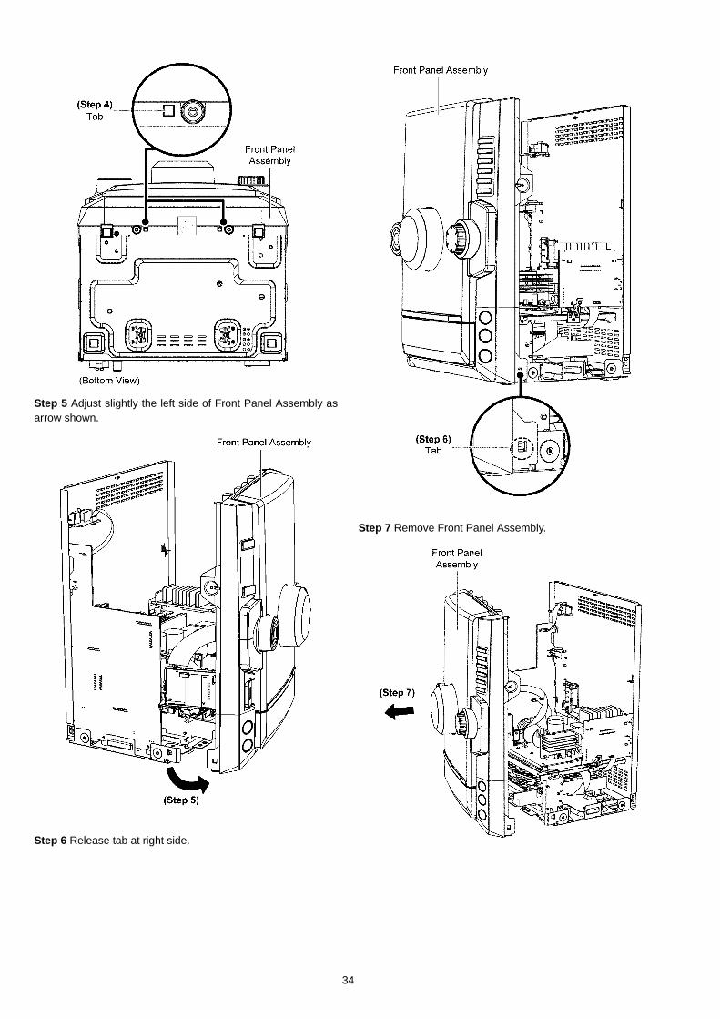
Step 5 Adjust slightly the left side of Front Panel Assembly asarrow shown.
Step 6 Release tab at right side.
Step 7 Remove Front Panel Assembly.
34

9.6. Disassembly of Panel P.C.B.• Refer to “Disassembly of Top Cabinet”.• Refer to “Disassembly of Front Panel Assembly”.
Step 1 Remove the Volume Knob.Step 2 Remove the Track Knob.
Step 3 Desolder 2 pins at the cable holder (JW6001) on PanelP.C.B..
Step 4 Remove 10 screws.
Step 5 Release catches by following the sequences (1-7).
35

Step 6 Slightly release Portion A of Panel P.C.B. from FrontPanel Assembly.Step 7 Remove Panel P.C.B..
Caution: During assembling, ensure that Panel P.C.B. is seated properly through the Guides & fully catched.
9.7. Disassembly of Remote SensorP.C.B.
• Refer to “Disassembly of Top Cabinet”.• Refer to “Disassembly of Front Panel Assembly”.• Refer to “Disassembly of Panel P.C.B.”.
Step 1 Remove Remote Sensor P.C.B..Caution: During assembling, ensure that Sensor P.C.B. is properly inserted & fully connected to Panel P.C.B..
36

9.8. Disassembly of CD Open But-ton P.C.B.
• Refer to “Disassembly of Top Cabinet”.• Refer to “Disassembly of Front Panel Assembly”.
Step 1 Desolder 2 pins (JW6201) on CD Open Button P.C.B..Step 2 Remove 1 screw.
Step 3 Lift up slightly and remove CD Open Button P.C.B. asarrow shown.
Caution: During assembling, ensure that the CD Open But-ton P.C.B. is properly located and seated under the guides.
9.9. Disassembly of USB P.C.B.• Refer to “Disassembly of Top Cabinet”.• Refer to “Disassembly of Front Panel Assembly”.
Step 1 Remove 2 screws.Step 2 Remove USB Unit.
37

Step 3 Desolder 3 pins.
Step 4 Remove USB P.C.B..
9.10. Disassembly of CD Lid• Refer to “Disassembly of Top Cabinet”.• Refer to “Disassembly of Front Panel Assembly”.
Step 1 Remove the spring as arrow shown in order ofsequence (1) to (3).Caution: During assembling, ensure that the spring is assembly at right position.
Step 2 Remove CD Lid as arrow shown.
38

9.11. Disassembly of Main P.C.B.• Refer to “Disassembly of Top Cabinet”.
Step 1 Detach 9P FFC at the connector (CN2705) on MainP.C.B..Step 2 Detach 12P FFC at the connector (CN2711) on MainP.C.B..Step 3 Detach 17P FFC at the connecter (CN2709) on MainP.C.B..Step 4 Detach 22P FFC at the connecter (CN2704) on MainP.C.B..Step 5 Detach 11P Cable at the connector (CN5802) on SMPSP.C.B..
Step 6 Remove 1 screw.
Step 7 Remove 1 screw.
Step 8 Detach Main P.C.B. from Rear Panel according to arrowshown.
39

Step 9 Detach 22P FFC at the connector (CN2706) on MainP.C.B..Step 10 Remove Main P.C.B..
Caution: During assembling, ensure that earth plate is bended flat against the Main P.C.B. properly when inserted to locators.
9.12. Replacement of Regulator IC (IC2701)
• Refer to “Disassembly of Main P.C.B.”.
9.12.1. Disassembly of Regulator IC(IC2701)
Step 1 Desolder pins of the Regulator IC (IC2701) on the sol-der side of Main P.C.B..
Step 2 Remove 1 screw.Step 3 Remove the Regulator IC (IC2701) from the Main P.C.B..Caution: Avoid touching the Small Heatsink due to its high temperature after prolong use. Touching it may lead to injuries.
40

9.12.2. Assembly of Regulator IC (IC2701)Step 1 Apply grease to the Small Heatsink.Step 2 Mount the Regulator IC (IC2701) on Main P.C.B..Caution: Ensure pins of the Regulator IC (IC2701) are prop-erly seated on Main P.C.B..Step 3 Screw the Regulator IC (IC2701) to the Small Heatsink.Caution: Ensure the Regulator IC (IC2701) is tightly screwed to the Small Heatsink.
Step 4 Solder pins of the Regulator IC (IC2701) on the solderside of Main P.C.B..
9.13. Disassembly of D-Amp P.C.B.• Refer to “Disassembly of Top Cabinet”.
Step 1 Remove 2 screws.
Step 2 Cut the Tie Wrap.Caution: During assembling, tie the 6P Cable Wire with the Tie Wrap to SMPS P.C.B. as diagram shown.Step 3 Detach 6P Cable Wire at the connector (CN5801) onSMPS P.C.B..
41
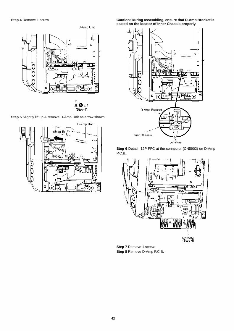
Step 4 Remove 1 screw.
Step 5 Slightly lift up & remove D-Amp Unit as arrow shown.
Caution: During assembling, ensure that D-Amp Bracket is seated on the locator of Inner Chassis properly.
Step 6 Detach 12P FFC at the connector (CN5902) on D-AmpP.C.B..
Step 7 Remove 1 screw.Step 8 Remove D-Amp P.C.B.
42

Caution: Keep the D-Amp Bracket in safe place, place it back during assembling.
9.14. Replacement of Audio DigitalAmp IC (IC5900)
• Refer to “Disassembly of D-Amp P.C.B.”.
9.14.1. Disassembly of Audio Digital AmpIC (IC5900)
Step 1 Desolder pins of the Regulator IC (IC5900) on the sol-der side of D-Amp P.C.B..
Step 2 Release 2 catches of Heatsink Clip.
Caution: During releasing of 2 catches, avoid touching the Heatsink, due to high temperature.
Step 3 Remove Heatsink Clip.Step 4 Remove Audio Digital Amp IC (IC5900).
43

9.14.2. Assembly of Audio Digital Amp IC(IC5900)
Step 1 Apply grease to the Heatsink.Step 2 Install the Audio Digital Amp IC (IC5900) on D-AmpP.C.B.Caution: Ensure pins of the Audio Digital Amp IC (IC5900) are properly seated on D-Amp P.C.B.Step 3 Install Heatsink Clip to the Heatsink.Caution: During assembling, ensure that Heatsink Clip is catched onto Heatsink properly.
Step 4 Solder pins of the Audio Digital Amp IC (IC5900) on thesolder side of D-Amp P.C.B..
9.15. Disassembly of SMPS P.C.B.• Refer to “Disassembly of Top Cabinet”.• Refer to “Disassembly of Front Panel Assembly”.
Step 1 Remove 1 screw.
Step 2 Cut the Tie Wrap.Caution: During assembling, tie the 6P Cable Wire with the Tie Wrap to SMPS P.C.B. as diagram shown.Step 3 Detach 6P Cable Wire at the connector (CN5801) onSMPS P.C.B..Step 4 Detach 11P Cable Wire at the connector (CN5802) onSMPS P.C.B..
44
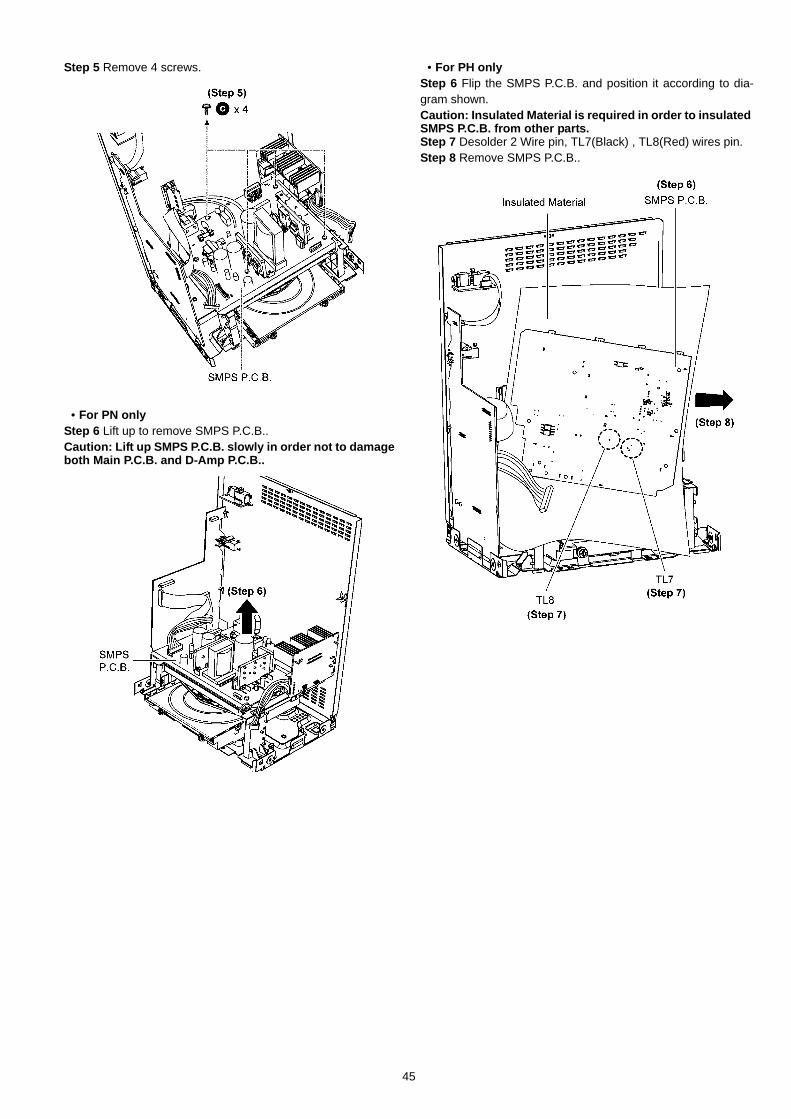
Step 5 Remove 4 screws.
• For PN only
Step 6 Lift up to remove SMPS P.C.B..Caution: Lift up SMPS P.C.B. slowly in order not to damage both Main P.C.B. and D-Amp P.C.B..
• For PH onlyStep 6 Flip the SMPS P.C.B. and position it according to dia-gram shown.Caution: Insulated Material is required in order to insulated SMPS P.C.B. from other parts.Step 7 Desolder 2 Wire pin, TL7(Black) , TL8(Red) wires pin.Step 8 Remove SMPS P.C.B..
45

9.16. Replacement of Switching Reg-ulator IC (IC5701)
• Refer to “Disassembly of SMPS P.C.B.”.
9.16.1. Disassembly of Switching Regula-tor IC (IC5701)
Step 1 Desolder pins of the Switching Regulator IC (IC5701) onthe solder side of SMPS P.C.B..
Step 2 Remove 1 screw from the Switching Regulator IC(IC5701).Step 3 Remove the Switching Regulator IC (IC5701) from theHeatsink A.Caution: Avoid touching the Heatsink A due to its high temperature after porlonged use. Touching it may lead to injuries.
9.16.2. Assembly of Switching Regulator IC (IC5701)
Step 1 Apply grease to the Heatsink A.Step 2 Install the Switching Regulator IC (IC5701) to the SMPSP.C.B..Caution: Ensure pins of the Switching Regulator IC (IC5701) are properly seated and soldered on SMPS P.C.B..Step 3 Screw the Switching Regulator IC (IC5701) to the Heat-sink A.Caution: Ensure the Switching Regulator IC (IC5701) is tightly screwed to the Heatsink A.
Step 4 Solder pins of the Switching Regulator IC (IC5701) onthe solder side of SMPS P.C.B..
46

9.17. Replacement of Rectifier Diode(D5702)
• Refer to “Disassembly of SMPS P.C.B.”.
9.17.1. Disassembly of Rectifier Diode(D5702)
Step 1 Desolder pins of the Rectifier Diode (D5702) on the sol-der side of SMPS P.C.B.Step 2 Desolder pins of the Heatsink A.
Step 3 Remove 1 screw from the Switching Regulator IC(IC5701).Step 4 Remove the Heatsink A with Rectifier Diode (D5702).Step 5 Remove 1 screw from the Rectifier Diode (D5702).Step 6 Remove the Rectifier Diode (D5702) from the HeatsinkA.
47

Caution: Avoid touching the Heatsink A due to its high temperature after prolonged use. Touching it may lead to injuries.
9.17.2. Assembly of Rectifier Diode (D5702)
Step 1 Apply grease to the Heatsink A.Step 2 Screw the Rectifier Diode (D5702) to the Heatsink A.Caution: Ensure the Rectifier Diode (D5702) is tightly screwed to the Heatsink A.Step 3 Install the Heatsink A with Rectifier Diode (D5702) onSMPS P.C.B. in the direction of arrow.Caution: Ensure the Heatsink A with Rectifier Diode (D5702) are properly seated on SMPS P.C.B.Step 4 Screw the Switching Regulator IC (IC5701) to the Heat-sink A.Caution: Ensure that Switching Regulator IC (IC5701) is tightly screwed to the Heatsink A.
Step 5 Solder pins of the Rectifier Diode (D5702) on the solderside of SMPS P.C.B..
Step 6 Solder pins of the Heatsink A on the solder side ofSMPS P.C.B..Caution: Ensure pins of the Rectifier Diode (D5702) are properly seated and soldered on SMPS P.C.B..
48

9.18. Replacement of RegulatorDiode (D5801)
• Refer to “Disassembly of SMPS P.C.B.”.
9.18.1. Disassembly of Regulator Diode(D5801)
Step 1 Desolder pins of the Regulator Diode (D5801) on thesolder side of SMPS P.C.B.
Step 2 Remove 1 screw from the Regulator Diode (D5801).Step 3 Remove the Regulator Diode (D5801) from the SMPSP.C.B..Caution: Avoid touching the Heatsink B due to its high temperature after prolonged use. Touching it may lead to injuries.
9.18.2. Assembly of Regulator Diode (D5801)
Step 1 Apply grease to the Heatsink B.Step 2 Install the Regulator Diode (D5801) on SMPS P.C.B.Caution: Ensure pins of the Regulator Diode (D5801) is properly seated on SMPS P.C.B.Step 3 Screw the Regulator Diode (D5801) to the Heatsink B.Caution: Ensure the Regulator Diode (D5801) is tightly screwed to the Heatsink B.
Step 4 Solder pins of the Regulator Diode (D5801) on the sol-der side of SMPS P.C.B..
49
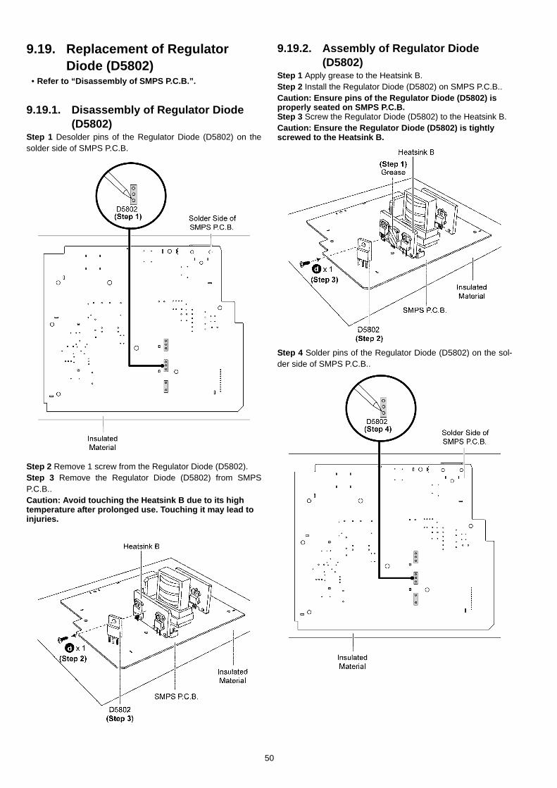
9.19. Replacement of Regulator Diode (D5802)
• Refer to “Disassembly of SMPS P.C.B.”.
9.19.1. Disassembly of Regulator Diode (D5802)
Step 1 Desolder pins of the Regulator Diode (D5802) on thesolder side of SMPS P.C.B.
Step 2 Remove 1 screw from the Regulator Diode (D5802).Step 3 Remove the Regulator Diode (D5802) from SMPSP.C.B..Caution: Avoid touching the Heatsink B due to its high temperature after prolonged use. Touching it may lead to injuries.
9.19.2. Assembly of Regulator Diode (D5802)
Step 1 Apply grease to the Heatsink B.Step 2 Install the Regulator Diode (D5802) on SMPS P.C.B..Caution: Ensure pins of the Regulator Diode (D5802) is properly seated on SMPS P.C.B.Step 3 Screw the Regulator Diode (D5802) to the Heatsink B.Caution: Ensure the Regulator Diode (D5802) is tightly screwed to the Heatsink B.
Step 4 Solder pins of the Regulator Diode (D5802) on the sol-der side of SMPS P.C.B..
50

9.20. Replacement of Regulator Diode (D5803)
• Refer to “Disassembly of SMPS P.C.B.”.
9.20.1. Disassembly of Regulator Diode(D5803)
Step 1 Desolder pins of the Regulator Diode (D5803) on thesolder side of SMPS P.C.B.
Step 2 Remove 1 screw from the Regulator Diode (D5803).Step 3 Remove the Regulator Diode (D5803) from the SMPSP.C.B..Caution: Avoid touching the Heatsink B due to its high temperature after prolonged use. Touching it may lead to injuries.
9.20.2. Assembly of Regulator Diode (D5803)
Step 1 Apply grease to the Heatsink B.Step 2 Install Regulator Diode (D5803) on SMPS P.C.B.Caution: Ensure pins of the Regulator Diode (D5803) are properly seated on SMPS P.C.B.Step 3 Screw the regulator diode (D5803) to the Heatsink B.Caution: Ensure the Regulator Diode (D5803) is tightly screwed to the Heatsink B.
Step 4 Solder pins of the Regulator Diode (D5803) on the sol-der side of SMPS P.C.B.
51

9.21. Disassembly of CD Mecha-nism Unit (DLS6C)
• Refer to “Disassembly of Top Cabinet”.• Refer to “Disassembly of Front Panel Assembly”.
Step 1 Remove 1 screw.
Step 2 Release the D-Amp Unit from Inner Chassis catch.
Step 3 Detach 12P FFC (CN5902) on D-Amp P.C.B..
Step 4 Detach 12P FFC at the connector (CN2711) on MainP.C.B..Step 5 Detach 11P Cable Wire at the connector (CN5802) onSMPS P.C.B..
52

Step 6 Remove 2 screws.
Step 7 Remove 3 screws (For PH only).Step 7 Remove 2 screws (For PN only).
Step 8 Detach Voltage Selector P.C.B. from Rear Panel asarrow shown (For PH only).
Step 9 Lift up SMPS Inner Chassis Unit.
53

Caution: During assembling, ensure that SMPS Inner Chassis Unit is catched onto Rear Panel properly.
Step 10 Detach 22P FFC from CD Mechanism Unit (DLS6C).Step 11 Remove 2 screws.Step 12 Remove CD Mechanism Unit (DLS6C).
9.22. Disassembly of Rear Panel• Refer to “Disassembly of Top Cabinet”.• Refer to “Disassembly of Tuner P.C.B.”.
Step 1 Remove 7 screws (For PH only).Step 1 Remove 6 screws (For PN only).
Step 2 Detach Voltage Selector P.C.B. from Rear Panel asarrow shown (For PH only).
54

Step 3 Lift up the SMPS Inner Chassis Unit to release the catchbetween the SMPS Inner Chassis Unit & the Rear Panel.
Step 4 Release 2 tabs.Step 5 Remove Rear Panel.
9.23. Disassembly of Voltage Selec-tor P.C.B. (For PH only)
• Refer to “Disassembly of Top Cabinet”. Step 1 Remove 1 screw.
Step 2 Detach Voltage Selector P.C.B. from Rear Panel asarrow shown.
55
Step 3 Desolder 2 Wire pins, TL5(Black), TL6(Red) on the Volt-age Selector P.C.B..Step 4 Remove Voltage Selector P.C.B..
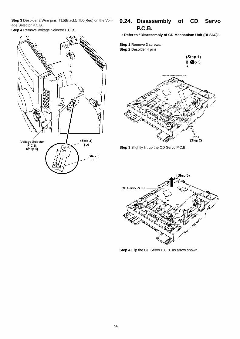
9.24. Disassembly of CD ServoP.C.B.
• Refer to “Disassembly of CD Mechanism Unit (DLS6C)”. Step 1 Remove 3 screws.Step 2 Desolder 4 pins.
Step 3 Slightly lift up the CD Servo P.C.B..
Step 4 Flip the CD Servo P.C.B. as arrow shown.
56

Step 5 Detach 16P FPC at the connector (CN7001) on CD Servo P.C.B..
57

10 Replacement of Traverse Unit10.1. Disassembling ProceduresStep 1 Release the guide.Step 2 Push the Traverse Slide Plate (rib), ensure both groovesare opened.
Step 3 Slide out the Traverse Unit as arrow shown.
Caution: Ensure the OPU is face upwards, avoid touching the surface of the traverse unit.
58

10.2. Assembling ProcedureCaution: Removal of the short pin is necessary for replace-ment of new traverse unit.
Step 1 Release the guide.Step 2 Push the Traverse Slide Plate (rib), ensure both groovesare opened.
59

Step 3 Slot the Traverse Unit at approximately 45° into themecha chassis as arrow shown.Caution: Ensure the bosses fix exactly onto the guides.
Step 4 Release the guide.Step 5 Push the Traverse Slide Plate (rib) to lock the TraverseUnit in.
60

11 Service PositionNote: For description of the disassembly procedures, seethe Section 9.
11.1. Checking and Repairing ofMain P.C.B.
Step 1 Remove Top Cabinet. Step 2 Main P.C.B. can be checked & repaired at its originalposition.
11.2. Checking and Repairing of D-Amp P.C.B.
Step 1 Remove Top Cabinet. Step 2 D-Amp P.C.B. can be checked & repaired at its originalposition.
11.3. Checking and Repairing ofPanel P.C.B.
Step 1 Remove Top Cabinet. Step 2 Remove Front Panel Assembly. Step 3 Attach 17P FFC to the connector (CN2709) on Main P.C.B.. Step 4 Attach 22P FFC to the connector (P901) on USB .P.C.B.. Step 5 Panel P.C.B can be chacked & repaired as diagram shown.
61

11.4. Checking and Repairing ofUSB P.C.B.
Step 1 Remove Top Cabinet. Step 2 Remove Front Panel Assembly. Step 3 Remove USB P.C.B.. Step 4 Position Front Panel Assembly as diagram shown. Step 5 Attach 17P FFC to the connector (CN2709) on Main P.C.B.. Step 6 Attach 22P FFC to the connector (P901) on USB P.C.B.. Caution: Insulated Material is required to insulate USB Unit from other parts.Step 7 USB P.C.B. can be chacked & repaired as diagram shown.
11.5. Checking and Repairing ofSMPS P.C.B.
Step 1 Remove Top Cabinet. Step 2 Remove Front Panel Assembly. Step 3 Remove 2 screws.(For PH only) Step 3 Remove 1 screw.(For PN only)
Step 4 Detach Voltage Selector P.C.B. from Rear Panel asarrow shown (For PH only).
Step 5 Cut the Tie Wrap. Step 6 Detach 6P Cable Wire at the connector (CN5801) onSMPS P.C.B.. Step 7 Detach 11P Cable Wire at the connector (CN5802) onSMPS P.C.B..
Step 8 Remove 4 screws.
62

Step 9 Remove SMPS P.C.B.. Caution:Lift up SMPS P.C.B. slowly in order not to damage both the Main P.C.B. & D-Amp P.C.B..
Step 10 Position Front Panel Assembly & SMPS P.C.B. as dia-gram shown. Caution: Insulated Material is required to insulate SMPS P.C.B. from other parts.Step 11 Attach 17P FFC to the connector (CN2709) on MainP.C.B.. Step 12 Attach 22P FFC to the connector (P901) on USBP.C.B..
Step 13 Extend the wire with extension Cable Wire(REXX1089) (11P Cable Wire from CN2701 to CN5802). Step 14 Connect 6P Cable Wire to the connector (CN5801) onSMPS P.C.B.. Step 15 SMPS P.C.B. can be checked & repaired as diagramshown.
63

12 Voltage & Waveform ChartNote:
• Indication Voltage Values are in standard values for the unit measured by the DC electronic circuit tester (high-impedance) withthe chassis taken as standard.Therefore, there may exist some errors in voltage values, depending on the internal impedance of the DC circuit tester.
• Circuit voltage and waveform described herein shall be regarded as reference information when probing defect point because itmay differ from actual measuring value due to difference of Measuring instrument and its measuring condition and product itself.
12.1. CD SERVO P.C.B.
REF NO.MODE 1 2 3 4 5 6 7 8 9 10 11 12 13 14 15 16 17 18 19 20
CD PLAY 0 0 0 0 0 0 0 0 0 0 0 0 0 0 0 0 0.3 0 1.6 3.2STANDBY 0 0 0 0 0 0 0 0 0 0 0 0 0 0 0 0 0 0 1.6 3.4
REF NO.MODE 21 22 23 24 25 26 27 28 29 30 31 32 33 34 35 36 37 38 39 40
CD PLAY 1.6 0 1.6 1.7 1.7 0 3.1 1.5 3.1 3.1 0 1.6 1.5 1.6 1.9 1.9 1.7 1.8 1.8 1.7STANDBY 1.7 3.4 1.7 1.7 1.7 0 3.4 1.5 3.4 3.4 0 1.7 1.6 1.7 1.7 1.7 1.7 1.7 1.7 1.7
REF NO.MODE 41 42 43 44 45 46 47 48 49 50 51 52 53 54 55 56 57 58 59 60
CD PLAY 0.2 2.4 1.9 1.7 1.2 1.8 3.2 1.2 1.3 1.3 1.7 1.7 0.9 1.5 1.5 1.5 0 3.0 1.5 0STANDBY 0 3.4 1.6 1.7 1.7 1.8 3.4 1.2 1.2 1.2 1.7 1.7 0.9 1.1 1.1 1.6 0 3.1 1.6 0
REF NO.MODE 61 62 63 64 65 66 67 68 69 70 71 72 73 74 75 76 77 78 79 80
CD PLAY 3.2 0 0 0 0 0 3.0 1.5 3.3 1.0 0.1 3.3 0 1.6 0 1.5 3.2 0 3.3 0STANDBY 3.4 0 0 0 3.3 0 3.3 0 3.3 0 0.1 3.3 0 1.6 3.4 1.5 3.4 0 3.4 0
REF NO.MODE 81 82 83 84 85 86 87 88 89 90 91 92 93 94 95 96 97 98 99 100
CD PLAY 0 3.3 0 0 0 0 0 0 0 0 0 0 3.2 0 0 0 0 0 0 0STANDBY 0 3.4 0 0 0 0 0 0 0 0 0 0 3.4 0 0 0 0 0 0 0
REF NO.MODE 1 2 3 4 5 6 7 8 9 10 11 12 13 14 15 16 17 18 19 20
CD PLAY 1.6 0 1.6 0 0 0 0 0 0 7.7 4.4 3.5 3.6 3.6 3.5 3.8 3.7 3.6 7.7 0STANDBY 1.7 0 1.7 3.3 0 0 0 0 0 7.7 4.0 4.0 3.6 3.6 3.6 3.6 3.6 3.6 7.7 0
REF NO.MODE 21 22 23 24 25 26 27 28 29 30
CD PLAY 7.7 0 0 0 7.7 1.6 1.6 1.6 0 0STANDBY 7.7 0 0 0 7.7 1.7 1.7 1.7 0 0
REF NO.MODE E C B
CD PLAY 3.1 2.0 2.4STANDBY 3.4 0 3.4
IC7002
Q7601
SA-AKX10PH/PN CD SERVO P.C.B.
IC7001
IC7001
IC7001
IC7001
IC7001
IC7002
64

12.2. Main P.C.B. (1/2)
REF NO.MODE 1 2 3 4 5 6 7 8 9 10 11 12 13 14 15 16 17 18 19 20
CD PLAY 4.7 4.7 4.7 4.7 4.7 4.7 4.7 4.7 4.7 4.7 4.7 4.7 4.7 0 4.7 9.4 0 3.3 3.3 0STANDBY 4.7 4.7 4.7 4.7 4.7 4.7 4.7 4.7 4.7 4.7 4.7 4.7 4.7 0 4.7 9.5 0 3.3 3.3 0
REF NO.MODE 21 22 23 24 25 26 27 28 29 30 31 32
CD PLAY 4.7 4.7 4.7 4.7 4.7 4.7 4.7 4.7 4.7 4.7 4.7 4.7STANDBY 4.7 4.7 4.7 4.7 4.7 4.7 4.7 4.7 4.7 4.6 4.6 4.6
REF NO.MODE 1 2 3 4 5 6 7 8
CD PLAY 6.1 6.1 6.1 0 6.1 6.1 6.1 12.2STANDBY 6.1 6.1 6.1 0 6.1 6.1 6.1 12.2
REF NO.MODE 1 2 3
CD PLAY 16.7 0 12.2STANDBY 16.7 0 12.2
REF NO.MODE 1 2 3 4 5
CD PLAY 16.7 5.2 0 1.0 2.9STANDBY 17.0 5.2 0 1.0 2.9
REF NO.MODE 1 2 3 4 5 6 7 8 9 10 11 12 13 14 15 16 17 18 19 20
CD PLAY 3.3 0 0 0 3.3 3.3 0 0 0 0.6 0.6 0 1.7 0 1.7 3.4 3.1 0 3.1 1.9STANDBY 3.3 0 0 0 3.3 3.3 3.3 0 0 0.7 0.7 3.3 1.7 0 1.7 3.4 3.4 3.3 0 2.1
REF NO.MODE 21 22 23 24 25 26 27 28 29 30 31 32 33 34 35 36 37 38 39 40
CD PLAY 0 0 0 0 0.1 0 0 0 3.3 3.3 0 0 0 0 3.3 0 0 0 0 0STANDBY 0 0 0 0 0.1 0 0 0 3.3 3.3 0 0 0 0 3.3 3.3 0 0 0 0
REF NO.MODE 41 42 43 44 45 46 47 48 49 50 51 52 53 54 55 56 57 58 59 60
CD PLAY 0 0 0 0 0 0 0 0 0 0 3.3 3.2 0 0 0 3.0 2.3 3.3 2.2 3.3STANDBY 0 0 0 0 0 0 0 0 0 0 3.3 3.2 0 0 0 3.3 0 3.3 0 3.3
REF NO.MODE 61 62 63 64 65 66 67 68 69 70 71 72 73 74 75 76 77 78 79 80
CD PLAY 3.3 3.3 3.3 0 0 3.3 0 0 0 0 0 0 0 0 0 0 0 0 0 3.3STANDBY 3.3 3.3 3.3 0 0 3.3 0 0 0 0 0 0 0 0 0 0 0 0 0 3.4
REF NO.MODE 81 82 83 84 85 86 87 88 89 90 91 92 93 94 95 96 97 98 99 100
CD PLAY 0 2.7 0.4 1.8 0 0 0 3.3 0 3.3 0 0 3.3 3.3 1.1 0 1.0 3.3 3.3 1.0STANDBY 0 2.8 0.4 1.9 0 0 0 3.3 0 2.3 0 0 3.3 3.3 1.2 0 1.1 3.3 3.3 1.1
IC2801
SA-AKX10PH/PN MAIN P.C.B.
IC2101
IC2801
IC2801
IC2801
IC2801
IC2101
IC2201
IC2701
IC2702
65

12.3. Main P.C.B. (2/2)
12.4. Panel P.C.B.
REF NO.MODE 1 2 3 4 5 6 7 8
CD PLAY 0 0 0 0 0 1.2 0 3.3STANDBY 0 0 0 0 0 1.2 0 3.3
REF NO.MODE E C B E C B E C B E C B E C B
CD PLAY 7.3 12.0 7.8 0 7.1 0 7.2 12.1 7.8 0 7.2 0 0 0 0STANDBY 7.2 12.1 7.8 0 7.1 0 7.2 12.1 7.9 0 7.1 0 0 0 0
REF NO.MODE E C B E C B E C B E C B E C B
CD PLAY 0 0 0 7.6 10.6 8.2 3.3 5.2 4.0 16.5 0 16.4 0 0 0.7STANDBY 0 0 0 7.6 10.6 8.2 3.3 5.2 4.1 16.7 0 16.8 0 0 0.6
REF NO.MODE E C B E C B E C B E C B E C B
CD PLAY 3.2 3.3 2.6 0 3.3 0.1 0.1 3.3 0 0 3.3 0 0 3.1 0STANDBY 3.3 3.3 2.6 0 3.3 0 0 3.3 0 0 3.3 0 0 3.3 0
REF NO.MODE E C B E C B E C B
CD PLAY 0 3.3 0 3.3 3.2 0.1 3.2 3.2 0.1STANDBY 0 0 3.0 3.3 3.3 0.1 3.4 3.4 0.1
QR2801
QR2832
IC2802
Q2302 Q2701 Q2702 Q2705 Q2790
Q2803 QR2704
SA-AKX10PH/PN MAIN P.C.B.
Q2220 Q2221 Q2222 Q2223 Q2301
QR2701 QR2702
QR2802 QR2831
REF NO.MODE 1 2 3 4 5 6 7 8 9 10 11 12 13 14 15 16 17 18 19 20
CD PLAY 0 0 0 0 2.3 1.4 0.4 2.8 1.9 0 0 0 3.4 -20.1 -20.1 -20.1 -24.0 -24.0 -24.0 -24.0STANDBY 0 0 0 0 2.3 1.4 0.4 2.8 1.9 0 0 0 3.4 -20.1 -20.1 -20.1 -24.0 -24.0 -24.0 -24.0
REF NO.MODE 21 22 23 24 25 26 27 28 29 30 31 32 33 34 35 36 37 38 39 40
CD PLAY -22.0 -23.9 -23.9 -23.9 -20.1 -22.0 -22.0 -23.9 -23.9 -24.3 -22.3 -22.2 -22.3 -22.3 -22.2 -22.2 -22.2 -22.2 -22.2 -22.2STANDBY -22.0 -23.9 -23.9 -23.9 -20.1 -22.0 -22.0 -23.9 -23.9 -24.3 -22.3 -22.2 -22.3 -22.3 -22.2 -22.2 -22.2 -22.2 -22.2 -22.2
REF NO.MODE 41 42 43 44
CD PLAY -22.2 -22.2 3.4 0STANDBY -22.2 -22.2 3.4 0
REF NO.MODE E C B
CD PLAY 0 16.5 -0.1STANDBY 0 16.7 -0.1
IC6001
SA-AKX10PH/PN PANEL P.C.B.
IC6001
IC6001
Q6101
66

12.5. USB P.C.B.
12.6. D-Amp P.C.B.
REF NO.MODE 1 2 3 4 5 6 7 8 9 10 11 12 13 14 15 16 17 18 19 20
CD PLAY 1.2 1.2 1.3 0 0 0 3.3 3.2 3.3 1.8 1.6 1.6 0 0 0 0 3.3 3.3 3.3 1.3STANDBY 1.1 1.1 1.1 0 0 0 3.2 3.2 3.3 1.5 1.4 1.5 0 0 0 0 3.3 3.4 3.4 1.2
REF NO.MODE 21 22 23 24 25 26 27 28 29 30 31 32 33 34 35 36 37 38 39 40
CD PLAY 0.9 1.3 1.3 1.2 1.2 1.2 1.3 1.3 1.2 1.3 1.3 1.3 1.3 1.3 1.2 1.2 1.1 3.3 1.0 0STANDBY 1.3 1.3 1.3 1.2 1.2 1.2 1.2 1.2 1.2 1.2 1.2 1.2 1.3 1.3 1.3 1.3 1.3 3.4 1.3 0
REF NO.MODE 41 42 43 44 45 46 47 48 49 50 51 52 53 54 55 56 57 58 59 60
CD PLAY 0.9 1.8 0.9 0 0.9 3.3 0.3 3.3 3.3 0 3.3 0.9 0 0 0.9 3.0 0 0 0 0.9STANDBY 1.3 1.8 1.3 0 1.3 3.3 0.3 3.3 3.4 0 3.4 1.3 0 0 1.3 3.3 0 0 0 1.3
REF NO.MODE 61 62 63 64
CD PLAY 0 1.8 0.9 3.3STANDBY 0 1.8 1.3 3.3
SA-AKX10PH/PN USB P.C.B.
IC900
IC900
IC900
IC900
REF NO.MODE 1 2 3 4 5 6 7 8 9 10 11 12 13 14 15 16 17 18 19 20
CD PLAY -30.0 -3.1 -3.1 34.9 0 -34.9 -26.4 35.2 6.1 -3.1 -35.1 -25.0 -35.1 -3.1 6.1 35.2 -34.9 -34.9 0 34.9STANDBY -30.0 -3.0 -3.0 34.9 0 -34.9 -26.4 35.2 6.2 -3.0 -35.1 -25.0 -35.1 -3.0 6.2 35.2 -34.9 -34.9 0 34.9
REF NO.MODE 21 22 23
CD PLAY -3.1 -3.1 4.6STANDBY -3.0 -3.0 2.5
REF NO.MODE E C B E C B E C B E C B E C B
CD PLAY -34.9 -34.9 -34.3 5.2 5.2 4.5 0 0 0.7 0 4.6 0 0 3.3 0STANDBY -34.9 -34.9 -34.3 5.2 5.2 4.5 0 0 0.7 0 0.1 0.7 0 3.3 0
REF NO.MODE E C B E C B E C B
CD PLAY 0 3.3 0 0 0 3.3 5.2 5.2 0STANDBY 0 3.3 0 0 0 3.4 5.2 5.2 0
SA-AKX10PH/PN D-AMP P.C.B.
IC5900
IC5900
Q5901 Q5902 Q5903 Q5905 Q5906
Q5907 QR5900 QR5901
67

12.7. SMPS P.C.B.
12.8. Tuner P.C.B.
REF NO.MODE 1 2 3 4 5 6 7
CD PLAY 164.8 0 0 19.1 0.1 1.4 0.5STANDBY 164.8 0 0 19.1 0.1 1.4 0.5
REF NO.MODE 1 2 3 4 5 6 7 8
CD PLAY 5.9 1.0 2.3 11.0 164.2 0 0 0STANDBY 5.9 1.0 2.3 11.0 164.2 0 0 0
REF NO.MODE 1 2 3
CD PLAY -2.0 -32.5 -35.2STANDBY -2.0 -32.6 -35.2
REF NO.MODE 1 2 3
CD PLAY 2.3 2.5 0STANDBY 2.3 2.5 0
REF NO.MODE E C B E C B E C B E C B E C B
CD PLAY 7.3 8.5 7.6 19.7 19.7 19.0 0 19.6 0.2 0 35.2 0 1.3 0 0.7STANDBY 7.4 8.6 7.7 19.7 19.7 19.0 0 19.6 0.2 0 35.2 0 1.3 0 0.7
REF NO.MODE E C B E C B E C B E C B E C B
CD PLAY 0 0 0.7 0 3.3 0 0 2.1 0.4 0 3.1 -3.0 0 3.3 6.6STANDBY 0 3.3 0 0 3.3 0 0 2.1 0.4 0 3.1 -2.9 0 3.3 6.6
REF NO.MODE E C B
CD PLAY 0 0.1 3.1STANDBY 0 0.1 3.1
Q5898
IC5701
IC5799
IC5801
IC5899
QR5801 QR5802
QR5810
SA-AKX10PH/PN SMPS P.C.B.
Q5720 Q5721 Q5722 Q5803 Q5860
Q5861 Q5862
REF NO.MODE 1 2 3 4 5 6 7 8 9 10 11 12 13 14 15 16 17 18 19 20
CD PLAY 0 0 3.0 3.0 0 0 0 0 0 0 3.3 3.3 1.4 0.3 0.3 0.3 0 0 0 0STANDBY 0 0 3.0 3.0 0 0 0 0 0 0 3.3 3.3 1.4 0.3 0.3 0.3 0 0 0 0
SA-AKX10PH/PN TUNER P.C.B.
IC52
68

12.9. Waveform Table
WF No. IC52-9,17 (PLAY)
0.2Vp-p(100usec/div)
WF No. IC52-13,14 (PLAY)
0.1Vp-p(200usec/div)
WF No. IC900-11 (PLAY)
2.2Vp-p(20nsec/div)
WF No. IC2101-2,12 (PLAY)
0.1Vp-p(200usec/div)
WF No. IC2101-6,8 (PLAY)
1.3Vp-p(200usec/div)
WF No. IC2801-10,11 (PLAY)
1.8Vp-p(10usec/div)
WF No. IC2801-13 (PLAY)
3.2Vp-p(20nsec/div)
WF No. IC2801-15 (PLAY)
2Vp-p(50nsec/div)
WF No. IC7001-80 (PLAY)
4.8Vp-p(20nsec/div)
WF No. IC7001-21 (PLAY)
1.8Vp-p(5usec/div)
WF No. IC7001-23,24 (PLAY)
0.52Vp-p(1usec/div)
WF No. IC7001-56,59 (PLAY)
2.4Vp-p(100usec/div)
WF No. IC7001-81 (PLAY)
1.9Vp-p(20nsec/div)
WF No. IC5900-10,14 (PLAY)
100Vp-p(1usec/div)
WF No. IC6001-5 (PLAY)
WF No. IC900-12 (PLAY)
3Vp-p(20nsec/div)
WF No. IC2101-31,32 (PLAY)
3.6Vp-p(200usec/div)
1.5Vp-p(1usec/div)
WF No. IC6001-8 (PLAY)
3.2Vp-p(2usec/div)
WF No. IC5900-2,3 (PLAY)
1.4Vp-p(1msec/div)
WF No. IC5900-21,22 (PLAY)
1.5Vp-p(500usec/div)
69

13 Illustration of ICs, Transistor and Diode
B0ACCK000012B1BACG000023MA2YF8000L
B0HFRJ000012
B0JCPD000025 MAZ8056GML
B0ZAZ0000052B0ABSM000008
C0DABFC00002
C0DAEMZ00001
B0EAKM000117B0EAMM000057
B0JAME000114B0HAMP000094
B0HCSP000001
B0BC019A0007B0BC035A0007B0BC6R100010B0BC9R000008
B0BC010A0007
B0FBAR000043
B0BC018A0267B0BC2R4A0263B0BC5R1A0266B0BC8R2A0266B0BC024A0269B0BC036A0264
BA5948FPE2 (28P)
C0DAAYG00001 (5P)
MN6627954AMA
(100P)
VUEALLPT031 (20P)
C1BA00000497 (23P)RFKWMAKX10PN
(100P)
C5HACYY00004 (7P)
C5HACYY00005 (7P)
MIP2F20MSSCF (8P)
B1AAJC000019
B1ABCF000176B1ABGC000005 B1ACKD000006
B1ADCE000012B1ADCF000001
B1BABG000007 B1BABK000001
B1GBCFJJ0051
B1GBCFJN0038
B1GBCFLL0037B1GDCFGA0018B1GDCFGG0026B1GDCFJJ0047
B0ADCJ000020
A
Ca
Cathode
Anode
A
Ca
Cathode
Anode
A
Ca
Cathode
Anode
A
Ca
Cathode
Anode
+~
~-
A
Ca
Cathode
Anode
A
Ca
Cathode
Anode
Cathode
Anode
A
Ca
C0AABB000125 (8P)
Ca
A
A
1 3 52 4
12
3
No.1No.1
C3EBFY000006 (8P)C1BB00001151 (32P)
No.1
8
4
5
7
12
3
C0HBB0000061 (64P)MNZSFB5KJM2 (64P)
No.1
EC
BB
CE
A
CA
ACA
CA
A
E
B
C
No.1
C0CAAKG00046
21
3E
BC
Cathode
AnodeA
Ca
A
Ca
Cathode
Anode
Ca
A
A
70

71
14 Simplified Block Diagram14.1. Overall Simplified Block Diagram
ASP IC
MICRO-PROCESSOR
IC
Tuner Silicon
FM/AM
SMPS
12V Reg
CD MCLK
AUX
Level meter
cct
Music Port
Supply
ctrl cct
Biased
amplifier
ASP Clk
ASP Data
Clip sensor
cct
SDIO
SDCLK
TU INT
TU RST
Headphone
Flash IC
LPF
HPF
safety
detection
cct
Regulator circuit
EEPROM
ICsele
cto
r
bass/ m
id/ tr
eble
SW
LPF
Clip
attenuation
Muting
cct
Muting
cct
witching
sformer
Fan signal
feedback
Fan
abnormal
detection
cct
Fan circuit
12V
Signal
detection
to microP
supply
To D-AMP
Power Supply
Sub trans
Rectifier
Mosfet
Switching IC
Sync cctto microP
for AC
detect
Feedback
cct
Speaker Units
H/P
AMP
Panel
FLCLK
FLData
FLCS
FL Driver
CD MDATA
CD MLD
CD STAT
CD RST
CD RESET SW
CD LOADING
CD OPEN SW
Blinking
LED Control
Single CD
DLS6 mecha
MicroP, LSI
Motor Drv
LOADER
FL s
tran
Key1
Key2
Vol Jog
Rotary Jog
LED Control From
microP
To microP
AD port
FL DISPLAY UNIT

72
14.2. D-Amp Block Diagram
FROM
SMPS
+/-VCC=33.8V,
24V(ECO enable)
+18V
(11.5V~19V)
BACKUP
+3.3V
DIGITAL AMP IC
(NXP)
REG
+12V12V
(245mA)(265mA)
(300mA) REG
+5V
+8.2V
(Discrete)
(200mA)
5V
7.5V
CD module motor
200mA)
ASP IC(30mA)
MIC MIXING AMP (15mA)
MIC IC (15mA)
BIG FAN1 (100mA)
BIG FAN2(100mA)
Bi-amp Filter(15mA)
HEADPHONE AMP(15mA)
SUBWOOFER AMP(15mA)
WIRELESS AMP(20mA)
WIRELESS+5V(300mA)
A) 9.5V
NI
5.2V
5.2V
(168mA) +3.3V
(Discrete)
JUPITAR MODULE(500mA)
LED LIGHTING X 13PCS(170mA)
DIGITAL TUNER(23mA)
JUPITER/USB MODULE(50mA)
CD+3.3V(75mA)
FL+3.3V(20mA)
mA)
250mA)40MA)
1A Max
(505mA)/830mA
PD =3.03W/4.98WHeatsink Needed
Block Connection Diagram
PANAMEX model
(60m
-Vp(20
FL1-(+FL2-(-2
FL DC-DC
CONVERTER
MCU SYSTEM(50mA)
KEY LINE(15mA)
REMOTE IR(15mA)
EEPROM(5mA)
(85mA)
(200mA)
DC-DC
+5.2V
(838mA)
1.5A Max

73
15 Block Diagram15.1. Servo/System Control
SA-AKX10PH/PN SERVO/SYSTEM CONTROL BLOCK DIAGRAM
: CD AUDIO INPUT SIGNAL LINE
810
CN6002CN2709
2SK
3DI
4DO
MICRO PROCESSORRFKWMAKX10PN
IC2801
EEPROMC3EBFY000006
X2802
X900
IC2802
46I2C CLK/WR END
48I2C DATA/ERROR
USBCONTROLLER
MNZSFB5KJM2
IC900
FL DISPLAY DRIVERC0HBB0000061
IC6001
FL DOUT 83 7DINFL DOUT
108
CN6002CN2709FL CLK 82
FL CLK
711
CN6002CN2709
76
CN5902CN2711
FL CS 84
XIN 15
XOUT 13
X2801
XCIN 10
XCOUT 11
EE CLK54
EE DAT55
USB SCL29
USB SDA30
RESET12
USBD-4
USBD+6
OSCI11
OSCO12
FL CS
117
CN6002CN2709
513
CN6002CN2709
33
CN6301CN6001RMT
315
CN6002CN2709 KEY2
FL DA
FL CLK
FL CS
8CLK
9STB
5
13
43
VDD
VDD
30 VEE
OSC
SG1
SG16
SG1
SG16
G1
G4
GR1
GR4
G5
G12
GR5
GR12
FL6001
FL DISPLAY
SERIAL
DATA
INTERFACE
OSC
COMMAND
DECODER
DISPLAYRAM
(24bits x 12 Words)
SEGMENT
DRIVER
GRID
DRIVER
MULTIPLEXED
DRIVER
OUTPUT
LATCH
SHIFT
REGISTER
DATA
SELECTOR
TIMINGGENERATOR
KEY MATRIXMEMORY
DIMMINGCIRCUIT
+3.3V
-VP
5V
1F+ F+
44F- F-
VREF
VREF
5V
REMOTE CONTROLSENSOR
Z6301
QR2801D2803
D2790
RESET
QR2831
SWITCH
RMT 18RMT
49
CN5902CN2711DCDET DAMP 5
DC DET AMP
11
CN5802ZJ2701*SYNC 20
SYNC
ASP-DATA 35ASP DA
ASP-CLK 36ASP CLK
F HOP1 4F HOP1
Q2790
SWITCH
85
CN5902CN2711MUTE F 3
MUTE F
310
CN5902CN2711MODE DA 6
MOD DA
73
CN51CN2705TUN SCLK 25
TUN SCLK
1111
CN5802ZJ2701*SMPS BP 49
AM BP
64
CN51CN2705TUN SIO 26
TUN SDIO
KEY2 93KEY2
216
CN6002CN270911
JW6201*ZJ6001A*KEY1
ROTARY JOG
KEY1 94KEY1
ROTARY JOG 88ROTARY JOG
414
CN6002CN2709 J VOLAVOL JOG 90
J VOLA
ASP CLK
PCONT 52PCONT
PCONT
CLIP ATTN 85CLIP ATTN
CLIP ATTN
CLIP SENS 86CLIP S
CLIP S
DCDET PWR 86DC DET PWR
DC DET PWR
DC DET AMP
ASP DA
3 3
P901 CN2704
6 6
P901 CN2704
14NRST CLK
USB SCL
47I2C REQ/WR START USB IRQ/WR START795 5
P901 CN2704 USB IRQ
51TERR TERR8014 14
P901 CN2704 USB TE
8CD NRST18 18
P901 CN2704 CD RST
57CD STAT10 10
P901 CN2704 CD STAT
64CD MLD17 17
P901 CN2704 CD MLD
58CD DATA11 11
P901 CN2704 CD MDATA
56CD CLK8 8
P901 CN2704 CD MCLK
STATUS59
BLKCK75
CD RST60
CD RESET SW61
CD OPEN SW66
USB SDA
USB RST33
MCLK56
CD LOAD CW(H)63
CD LOAD CCW(L)65
19 19
P901 CN2704
50VERR VERRUSB VE
784 4
P901 CN2704
MDATA OUT57
MLD58
USB PORTP903
2D-
3D+
1VBUS
MANUAL EQS6006
REWINDS6008
ALBUM+S6009
ALBUM-S6010 CD
PLAY/PAUSE
S6011
FORWARDS6007
POWERS6001
AUXS6003 USB
PLAY/PAUSE
S6004
D.BASSS6005
TRACK JOGVR6002
VOLUME JOGVR6001
STOP/-DEMOS6002
FM/AMS6012
OPEN/CLOSES6201
FROM/TO
POWER AMPLIFIER
FROM/TO
AUDIO
FROM/TO
AUDIO
FROM/TO
POWER SUPPLY
FROM/TO
POWER SUPPLY
MAIN P.C.B.
USB P.C.B.
PANEL P.C.B.
TUNER P.C.B.
D-AMP P.C.B.
SMPS P.C.B.
CD OPENBUTTON P.C.B.
REMOTESENSOR P.C.B.
: USB SIGNAL LINE
+
+
3.3V
Q7601
LASER DRIVE
X7201
67MCLK
SERVOPROCESSOR
MN6627954AMA
IC7001
TRVP23
SPOUT21
PC22
TRP24
X181
X280
59OUTR
3IN1
4PC1
DRIVERBA5948FPE2
IC7002
D2-13
D2+14
D1-11
D1+12
D3-15
D3+16
D4-17
LD42
PD41
D4+
F+
F-
T+
T-
LD
LPD
A40
C39
D37
A
B38B
18
27IN4
FOP2528IN3
1IN2
70STAT11 12
CN7002 CN2706 CD STAT
71BLKCK10 13
CN7002 CN2706 CD BLKCK
72NRST9 14
CN7002 CN2706 CD RST
5 18
CN7002 CN2706 CD RESET SW
3 20
CN7002 CN2706 CD OPEN SW
20 3
CN7002 CN2706
56OUTL22 1
CN7002 CN2706
CD MCLK
14 9
CN7002 CN2706
4 19
CN7002 CN2706
68MDATACD MDATA
13 10
CN7002 CN2706
69MLDCD MLD
CD LOADING
12 11
CN7002 CN2706
OPTICAL PICKUP UNIT
16
CN7001
15
CN7001
14
CN7001
13
CN7001
7
CN7001
9
CN7001
E35E
F36F
3
CN7001
2
CN7001
4
CN7001
11
CN7001
ACTUATOR
PHOTO
DIDE
LASER
DIODERESETS7201
CD OPENS7202
TRAVERSE MOTORM7301*
SPLINDLE MOTORM7302*
TO AUDIO
CD SERVO P.C.B.

74
15.2. Audio
SA-AKX10PH/PN AUDIO BLOCK DIAGRAM
: AUX AUDIO INPUT SIGNAL LINE : AUDIO OUTPUT SIGNAL LINE: CD AUDIO INPUT SIGNAL LINE : AM SIGNAL LINE : AM/FM SIGNAL LINE: FM SIGNAL LINE
X51
1
2
FM ANT
JK51
46
CN2705CN51
37
CN2705CN51
82
CN2705CN51
64
CN2705CN51
FM/AM RADIO RECEIVERVUEALLPT031
IC52
ASPC1BB00001151
IC2101
L CH 3
R CH 13
TU-L
TU-R
LOUT
ROUT
LOUT 14
ROUT 13
SDIO 8
SCLK 7
2 FMI 12 INL2
2 INR2
17 DCLK
9 RCLK
AM ANT
JK52 L52
4
6
3
1
2
4 AMI
CLIP S
CLIP ATTN
2 1
6 7
OP-AMPC0AABB000125
IC2201
Q2220
AMP
Q2221
SWITCH
Q2223
SWITCH
CLIP SENSORCIRCUIT
Q2302
SWITCH
Q2301
SWITCH
Q2222
121
CN5902CN2711FRONT L
103
CN5902CN2711FRONT R
AMP
FROM/TO
SERVO/SYSTEM CONTROL
TO
POWER AMPLIFIER
FROM/TO
SERVO/SYSTEM CONTROL
MAIN P.C.B.
D-AMP P.C.B.
TUNER P.C.B.
122
CN2706CN7002
R
L
AUX IN
JK2801
3
1
2AUX-L
10 INL4
AUX-R4 INR4
CD-L8 DIFFL
320
CN2706CN7002 CD-R6 DIFFR
18 SCL
19 SDA
ASP CLK
ASP DA
FROM
SERVO/SYSTEM CONTROL
FROM/TO
SERVO/SYSTEM CONTROL
CD SERVO P.C.B.

75
15.3. Power Amplifier
SA-AKX10PH/PN POWER AMPLIFIER BLOCK DIAGRAM
POWER AMPLIFIERC1BA00000497
IC5900
121
CN5902CN2711
OUT110
BOOT1
VD
DP
1
VS
SP
1
VS
SP
2
VD
DP
2
9
8
13
11
16
VD
DA
1
VD
DA
2
VS
SA
1
VS
SA
2
4
6
20
18
VS
SD
17
2IN1+
1OSC
INPUT
STAGE
PWM
MODULATOR RELEASE1
ENABLE1
ENABLE2
SWITCH1
MUTE
DRIVER
HIGH
DRIVER
LOW
CONTROL
&
HANDSHAKE
OUT214
BOOT215
PROT7
FL IN
CN5902CN2711 MOD DA
103
CN5902CN2711 FR IN
INPUT
STAGE
MODE
12STABI
STABI
PWM
MODULATOR
OSCILLATOR MANAGERTEMP. SENSOR
CURRENT PROTECTION
VOLT. PROTECTION
RELEASE2
SWITCH2
MUTE
DRIVER
HIGH
DRIVER
LOW
CONTROL
&
HANDSHAKE
-30V
30V
-30V
-30V
30V -30V
-30V 30V
Q5906,Q5907
DC DETECT
Q5902,Q5903,Q5905
+
-
3
JK5901
4
JK5901
+
-
FRONT (RIGHT)
FRONT (LEFT)
1
JK5901
2
JK5901
: AUDIO OUTPUT SIGNAL LINE
FROM AUDIO
D-AMP P.C.B.
MAIN P.C.B.
21IN2-
85
CN5902CN2711 MUTE F
310
49
CN5902CN2711 DC DET
23MODE
5V
5V
MUTINGCIRCUIT
QR5900,QR5901
SWITCH
Q5901
SWITCH
TH5900
76
CN5902CN2711 FHOP1
FROM/TO
SERVO/SYSTEM CONTROL

76
15.4. Power Supply
SA-AKX10PH/PN POWER SUPPLY BLOCK DIAGRAM
AC INLETP5701
F1
DZ5701
5,65,6
ZJ5901*CN5801
11
ZJ2701*CN5802153
CN6002CN2709
612
CN6002CN2709
+30V SENSE VDD
22
ZJ2701*CN5802SYS3.3
FB 2
VDD 1
D 5
SWITCHING POWERSUPPLY CONTROL
MIP2F20MSSCF
IC5799
5
VCC 4
CL 3
6
3
4
2
1
3
2
1
SUBTRANSFORMER
T5751
7
8
10
T5701
SWITCHINGTRANSFORMER
T6101
8
9
5
1
3
TH5702
TH5860
D5701
L5703
3
2
4
1
D5896
D5798D5795
4
D2710
D2709
-30V SENSE
D6103
D6101
DC 18V
CD 3.3V
VP DET
DVREF+
VREF+
QR5802
QR5801
POWERCONTROL
Q5860,Q5861,Q5862
TRANSFORMERTEMP. DETECT
Q6101
POWER SAVECONTROL
Q5898
SYNCSWITCH
Q2701
D2711
REGULATOR
Q2803
POWERSUPPLY
QR2802
POWERCONTROL
QR5810
INVERTER
PC5799FEED BACK
3
4
2
1
PC5701FEED BACK
1
2
4
3
PC5702SYNC SWITCH
FOR PH
VDD
1,21,2
ZJ5901*CN5801 VSSVSS
IC2701
1 IN
VOLTAGEREGULATOR
C0CAAKG00046
OUT 3
IC2702
1 VCC
SWITCHINGREGULATOR
C0DAAYG00001
OUT 2
IC5899
1 C
SHUNTREGULATOR
C0DAEMZ00001
R 2
-VP
F+
F-
DVREF
126
CN6002CN2709
135
CN6002CN2709
3.3V
VCC
DC DET PWR
PCONT
3.3V
DVREF
117
CN6002CN2709VREF
55
CN51CN27053.3V
22
CN6301CN6001VREF
122
CN7002CN27067.5V
7,8,194,15,16
CN7002CN27063.3V
5V
Q2702
CURRENTCONTROL
QR2704
DC DETECT
QR2701,QR2702
DC DETECT
Q2705
CURRENTLIMITER
5V
DC DET AMP
11
P901CN2704
3.3V2121
P901CN2704
3.3V
211
CN5902CN27115V
TOSERVO/SYSTEM CONTROL
FROMSERVO/SYSTEM CONTROL
FROM SERVO/SYSTEM CONTROL
TO SERVO/SYSTEM CONTROL
TO SERVO/SYSTEM CONTROL
99
ZJ2701*CN5802PCONT
44
ZJ2701*CN5802DC DET
7,87,8
ZJ2701*CN5802DC18V
1111
ZJ2701*CN5802AM BP
SMPS P.C.B. MAIN P.C.B.
D-AMP P.C.B.
PANEL P.C.B.
REMOTE SENSOR P.C.B.
CD SERVO P.C.B.
USB P.C.B.
D-AMP P.C.B.
TUNER P.C.B.
AC INLET P.C.B.
SHUNTREGULATOR
C0DABFC00002
IC5801
5
4
1
2
16
11
MAINTRANSFORMER
17
14
15
13
12
7
8
5
4
1
2
16
11
12
17
14
15
13
7
6
8
5
4
1
2
16
11
12
17
14
15
13
7
6
8
D5731D5729
D5726
D5802
D5803
D580
D5801
D5724D5727
DC DETECT
FEED BACK
CIRCUIT
Q5721
SWITCH
Q5803
AMBP SWITCH
Q5720,Q5722
CURRENTLIMITINGSWITCH
4
3
1
2
PC5720
HOT COLD
FEED BACK
SWITCHINGREGULATOR
C5HACYY00005...PH
FOR PH FOR PN
C5HACYY00004...PN
IC5701
VCC 4
OCP/BD 7
FB 6
GND 3
D 1
VOLT ADJS5701
VOLTAGESELECTOR P.C.B.

77
16 Wiring Diagram
SA-AKX10PH/PN WIRING CONNECTION
C PANEL P.C.B.(SOLDER SIDE)
B MAIN P.C.B.(SOLDER SIDE) D CD OPEN BUTTON P.C.B.
(SOLDER SIDE)
E REMOTE SENSOR P.C.B.(SOLDER SIDE)
J VOLTAGE SELECTOR P.C.B.(SOLDER SIDE)
I SMPS P.C.B.(SOLDER SIDE)
F TUNER P.C.B.(SIDE B)
PbF
PbF
PbF
PbF
PbF
PbF
S5701
(FOR PH ONLY)
VOLT ADJ
RED BLKTL6* TL5*
(VOLTAGE SELECTOR)
321
JK52JK51
CN51
1 12
12
98
AM ANT FM ANT
CN2704
CN2706
CN2705
CN2711
CN2707
CN2709
FOR DEBUG
AUX
21 21
22
2 1
2122
21
2122
21
89 21
89
2
3
14
21
1112
12
78 1 2
1716
VR6001
CN6002
VR6002
ZJ6001A*
T6101
TRACK
CN6001
(SWITCHINGTRANSFORMER)
VOLUME
12
1716
12
1716
1
32
1 2
1 2
3
98 7 6
54
321
14
ZJ6001B*1
2
CN6301 Z6301
SENSOR4
1 321
(MAIN TRANSFORMER)
CN5802
T5751
P5701
T5701
(SUB TRANSFORMER)
TL7*BLK
TL8*RED
CN5801
120V 60Hz...PN 110V-127V/
220V-240V50/60Hz...PH
AC IN
1
11
10
7
8
9
6
5
4
3
2
1
1 18
4
2
8
9 10
7
6
5
11
12
13
14
15
16
17
16
JK2801
ZJ2701*111
NOTE: " * " REF IS FOR INDICATION ONLY.
CN7001
CN70021 2
15 16
2221
21
OPTICAL PICKUP UNIT
H D-AMP P.C.B.(SOLDER SIDE)
G USB P.C.B.(SOLDER SIDE)
A CD SERVO P.C.B.(SOLDER SIDE)
PbF
PbF
PbF
PbF
P901P903
USB PORT
4321
5
612
2221
CN5902
SPEAKERS
21 11
12
2111
12
1
2
3
4
JK5901
ZJ5901*
6
1

78

17 Schematic Diagram Notes• This schematic diagram may be modified at any time
with the development of new technology.Notes:
• Important safety notice:
Components identified by mark have special characteris-tics important for safety.Furthermore, special parts which have purposes of fire-retar-dant (resistors), high quality sound (capacitors), low-noise(resistors), etc are used.When replacing any of components, be sure to use onlymanufacturer’s specified parts shown in the parts list.
• In case of AC rated voltage Capacitors, the part no. and val-ues will be indicated in the Schematic Diagram.AC rated voltage capacitors:For PN only:C5701, C5703, C5704, C5705, C5708For PH only:C5701, C5703, C5704, C5705, C5706, C5707. C5708
• ResistorUnit of resistance is OHM [Ω] (K=1,000, M=1,000,000).
• CapacitorUnit of capacitance is µF, unless otherwise noted. F=Farads,pF=pico-Farad.
• CoilUnit of inductance is H, unless otherwise noted.
• *REF IS FOR INDICATION ONLY.
• Voltage and signal line
• For PH only
• For PN only
S5701: Voltage ADJ switch (For PH only).S6001: Power switch ( ).S6002: Stop ( -DEMO) switch. S6003: AUX SwitchS6004: USB Play/Pause (USB / ) switch.S6005: D.BASS switch.S6006: Manual EQ (MANUAL EQ) switch.S6007: Forward ( / ) switch.S6008: Rewind ( / ) switch. S6009: Album + switch.S6010: Album - switch.S6011: CD switch ( ).S6012: FM/AM switch.VR6001: Volume Jog.VR6002: Track Jog.
: +B signal line
: -B signal line
: CD Audio input signal line
: AUX input Audio signal line
: Audio output signal line
: USB signal line
: FM/AM signal line
: AM signal line
: FM signal line
79

80

81
18 Schematic Diagram18.1. CD Servo Circuit
A
1 2 3 4 5 6 7 8 9 10 11 12 13 14
8 9 10 11 12 13 14
C
B
A
C
D
B
E
G
H
F
A CD SERVO CIRCUIT
SCHEMATIC DIAGRAM - 1
SA-AKX10PH/PN CD SERVO CIRCUIT
: CD AUDIO INPUT SIGNAL LINE: +B SIGNAL LINE
BTOMAIN CIRCUIT
(CN2706)
IN SCHEMATIC
DIAGRAM - 3
22
1
50V1C7227
MAZ80560MLD7650
50V1C7228
1KR7217
C7218
0.0
82
820
R7212
C72170.1
C7225
1000P
R72181K
C7226
1000P
100R7221
C72300.1
C72316.3V220
82KR7211
0.1C7263
LB
7262
000LB
7264
LB
7263
C7241
1000P
C7216680P
C72440.015
2 0.47
16V10C7235
C71610.1 C7234
0.1
C7221
15P
C7222
15P
10
C7164
10
C7165
C7232
6.3
V220
1KR7254
470P
C7253
C7166
0.0
1
0.1
C7233
10R7253
R7214
470
1MR7220
H0H169500013X7201
S7202CD OPEN
0.1C7243
6
5
8
9
11
12
10
18
15
17
16
20
19
13
14
7
2
1
4
3
22
21
CN7002
S7201REST SW
0.022
C7264
0.1
79
77
76
78
49
47
48
50
7471 7267 685655 58575251 5453 65 6661 6259 60 6463 7069 73 75
10 8 7912 11
99
100
95
94
96
97
90
91
89
93
92
98
46 5 2 13
81
82
80
86
87
88
84
83
85
45
19 17 15 141618
43
23 21 2022
41
24
39
37
33
35
34
29
30
27
26
28
32
31
36
38
25
40
42
44
13
46
MN6627954AMAIC7001
C7601
6.3
V33
4.7
R7601
C76146.3V100
C7670
0.1
C7626
0.1
B1ADCF000001Q7601
5.6R7650
LASER DRIVE
C7613 0.1
6
5
8
9
10
12
11
7
2
1
4
3
14
13
16
15
CN7001
TO OPTICALPICKUP UNIT
28(VREF)
A. GND
LCH OUT
TX
MCLK
RST
3.3V
STAT
7.5V
MLD
LD SW
P. GND
D. GND
BLKCK
MDATA
3.3V
REST SW
LOADING
CD OPEN SW
RCH OUT
SRDATA (ST_IN)
BCLK (ST_CLK)
LRCK (ST_REQ)
[51] ARFIN
IRE
F
OU
TR
OU
TL
TX
MLD
MC
LK
NR
ST
ST
AT
FLA
G
PLLF
DVDD2
AV
SS
1
DV
SS
3
BLK
CK
MD
AT
A
AV
DD
1
PLLF
0
ARFFB
[52] DSLF
[74] SMCK
[75] PMCK
[1] A9
[2] A11
[24] TRP
SERVO PROCESSOR
[25] FOP
RFIN X2
X1
NTEST2
A
B
F
E
D
C
PD
LD
D5
D7
D8
D9
D15
D13
D11
D10
D12
D14
D6
SDRCK
DRVDD
VREF
TR
VP
BA
1
A0
A2
A4
A6
A8
A7
A5
A3
A1
A10
NW
E
BA
0
PC
NR
AS
NC
AS
PR
AM
VD
D33
PR
AM
VD
D15
PR
AM
VS
S33
SP
OU
T
NTEST
D1
D3
D4
D0
D2CENV
AVDD2
RFENV
AVSS2
IODD2
DVSS1
DVDD1
OSCIN
RFOUT
IODD1
DVSS2DQ
SY
TX
T
ARFDC
NS
RV
MO
NO
N
EX
T1 / L
RC
K (
ST
_R
EQ
)
EX
T2 / B
CLK
(S
T_C
LK
)
EX
T0 / S
RD
AT
A (
ST
_IN
)
F
A
B
E
GND
T-
F-
F+
T+
LPD
VREF
LD GND
GND (GUARD)
GND (GUARD)
LD
VCC
ARFOUT
CTRCRS
SRVMON0
SRVMON1
TP
51(ARF)TP
24TP
19TP
16TP
14TP
18TP
4TP
3TP
2TP
1TP
87TP
86TP
10TP
11TP
31TP
13TP
9TP
8TP
7TP
12TP
17TP
1 2 3 4 5 6 7
D
E
G
H
F
C72236.3V4.7
C710
0.1C7204
C72036.3V220
C7315
0.4
7
88
C7339
0.0
18
10KR7328
3.3KR7315
R7330
5.6
K
10KR7111
C7142 3300P
C7107
C7155 0.1
0.1C7154
+
M7302*SPINDLE MOTOR
DRIVER
39
+
M7301*
TRAVERSE MOTOR
C733410V220
C73350.1
100R7335
10
R7336
1KR7332
27KR7331
6.8KR7323
330R7325
1KR7327
18KR7349
1KR7329
C7352
0.0
18
C7338
0.0
27
1K
R7339
GN
D1
191817 2015 16
14 12 9 811 1013
22 233021 282724 25 26
2 16729 345
IC7002BA5948FPE2
PV
CC
1
D4+
D1-
PV
CC
2
NC
NC
NC
NC
NC
NC
NC
IN2
NC
PC
1
PC
2
IN1
GN
D
PG
ND
1
FO
GA
IN
GN
D
IN4
IN3
VC
C
VR
EF
PG
ND
2
D3+
D2-
D3-
D2+
D1+
D4-
TR
V G
AIN
90TP
TP 38TP 36TP
37TP
TP
50TP
89TP

82
18.2. Main Circuit
A
1 2 3 4 5 6 7 8 9 10 11 12 13 14
C
D
B
B MAIN CIRCUIT
SCHEMATIC DIAGRAM - 2
SA-AKX10PH/PN MAIN CIRCUIT
2/4
4/4
1/4
3/4
TO MAINSECTION (2/4)
(3/4)
P1
: CD AUDIO INPUT SIGNAL LINE : AUX AUDIO INPUT SIGNAL LINE : AM/FM SIGNAL LINE: AUDIO OUTPUT SIGNAL LINE: -B SIGNAL LINE: +B SIGNAL LINE
DV
RE
F+
100R2880
22
KR
28
90
EE
_C
S
R28873.9K
R287547K
R28883.9K
206
R287410K
10
0R
28
42
R2
83
81
K
1K
R2
84
9
1.5
KR
28
54
D2
80
1B
0A
CC
K0
00
01
2
D2
80
2B
0A
CC
K0
00
01
2
1K
R2
85
1
10
0R
28
52
0.1C2804
R2
85
51
.5K
1K
R2
87
1
10
0R
28
69
R2
85
81
00
R2
86
31
K
R2
86
61
K
R2
86
01
K
R2
86
41
00
R2
86
21
00
FL_CS
FL_CLK
10KR2817
ME
AGND
1K
R2
83
6
R2826 47K
10KR2827
R2829 100FL_DA
R2828 100
V_JOG_A
R2830 100
R2831 100ROTARY_JOG
CLIP_S
CLIP_ATTN
1.2K...PH0...PN
R2816
R2821 1K
80 78 767779
87
86
88
89
82
84
83
81
85
90
69 67 65 64666870 51
49
45
47
46
41
44
42
43
48
50
53555762 60 596163 58 56 54 5275 73 717274
IC2801
PC
ON
T
EE
_C
LK
EE
_C
S
DC
_D
ET
_P
WR
CD
_M
LD
CD
_M
CL
K
CD
_M
DA
TA
EE
_D
AT
47KR2825
0R2130
US
B_
TE
US
B_
IRQ
US
B_
VE
CD
_B
LK
CK
CD
_L
OA
DIN
G
CD
_S
TA
T
CD
_R
ES
T_
SW
CD
_R
ST
CD
_O
PE
N_
SW
D2804B0BC5R1A0266
B1ACKD000006POWER SUPPLY
Q2803
470KR2893
EE
_D
AT
10KR28943
30
PC
28
11
EE
_C
LK
22
KR
28
92
C2
81
23
30
P
ASP_CLK
7
8
5
6
2
1
4
3
C3EBFY000006EEPROM
IC2802
AM_BP
C28160.022
VREF+
TXD
CLK
USB_RST
RXD
ASP_DA
BUSY
R28894.7K
B0
AC
CK
00
00
12
D2
80
3
R28911K
PCONT
DRVREF+
QR2802B1GBCFLL0037
POWER CONTROL
C281050V3.3
GBCFLL0037RESET
QR2801
SYS3.3V
NC
TEST
VCC
GND
SK
CS
DO
DI
NC
NC
NC
CD
_O
PE
N_
SW
HE
AD
PH
ON
E_
SW
[82] FL_CLK
BL
KC
K
NC
VE
RR
NC
[83] FL_DOUT
NC
NC
NC
NC
[81] MMOD0
NC
NC
PC
ON
T/E
FP
/CE
EE
_C
S/E
FP
/EP
M
EE
_D
AT
EE
_C
LK
NC
NC
NC
NC
NC
NC
VS
S
CD
_L
OA
D(H
)(T
RV
_S
W)
CD
_L
OA
D(L
)(T
RV
_C
CW
)[49] SMPS_BP
[50] NC[51] DCDET_PWR
ML
D
MC
LK
ST
AT
US
MD
AT
A_
OU
T
VC
C
/RE
SE
T_
SW
(IN
NE
R_
SW
)
CD
_R
ST
VOL_JOG
FL_CS
NC
TE
RR
ROTARY_JOG
US
B_
RE
QW
R_
ST
AR
T
CLIP_ATT
CLIP_SENSOR
REG
BUSY
CNVSS
TXD
CLK
RXD
5
6
1
3
4
2
8
7
CN2707
FOR DEBUG
RESET
RXD
TXD
VCC
EFM
BUSY
CNVSS
/RESET
CLK
E
G
H
F
TO MAINSECTION
47KR2883 C2805
0.1 6.3V2C280
100R2881
100R2882
R2886 100
R2885 100
100R2884
10
0R
28
43
10
0R
28
39
22
KR
28
40
10
0R
28
41
22
KR
28
73
C2
80
30
.1
10
0R
28
46
10
KR
28
59
10
0R
28
57
10
0R
28
72
10
0R
28
70
10
0R
28
65
10
0R
28
68
10
0R
28
67
1K
R2
85
6
220R2853
1MR2850
R2
83
51
0K
R2
83
44
7K
KEY1
F_HOP2
F_HOP1
CD3.3V
KEY2 R2824 100
R2822 100
R2815 3.3K
3 42 5
98
94
95
92
91
93
97
96
1
100
99
1614 15 1711 1312 30
39
37
35
32
31
34
33
36
38
40
22 2320 21 26 282724 2518 19 29976 8 10
RFKWMAKX10PNMICRO PROCESSOR
QR2832B1GDCFGG0026
SWITCH
QR2831B1GDCFGG0026
SWITCH
R2878 15K C2
80
71
R2877 15K
R2879 10K
3
1
2
H2
B1
00
50
00
04
X2
80
2
R281022K
R284710M
H0
A3
27
20
00
97
X2
80
1
18PC2801
22PC2802
0R2848
TU
N_
SD
IO
B1D
GN
D
TU
N_
RS
T
TU
N_
SC
LK
US
B_
SD
A
SY
NC
US
B_
SC
L
TU
N_
GP
10
2
RM
T
DC
_D
ET
_A
MP
CN
VS
S
MO
D_
DA
MU
TE
_F
RE
SE
T
XO
UT
VS
S
XIN
BY
TE
CN
VS
S E
FP
_C
NV
SS
XC
IN
XC
OU
T
/RE
SE
T
[99] AVCC
F_
HO
P
DC
DE
T_
DA
MP
MU
TE
_A
MO
DE
_D
A
[100] DEMO_SEL
MU
TE
_F
[98] VREF
RM
T
VC
C
NC
NC
ASP_CLK
NC
NC
TU
NE
R_
DA
TA
NC
NC
ASP_DAT
BUSY
USB_RST(CLK)
RXD
TXD
TU
NE
R_
INT
NC
SY
NC
/NM
I
NC
[30] USB_SDA(TXD)[29] USB_SCL(RXD)
NC
TU
NE
R_
CL
K
TU
NE
R_
RS
TAVSS
BASS_JOG2
NC
NC
CS
NC
BASS_JOG1
KEY2
KEY1
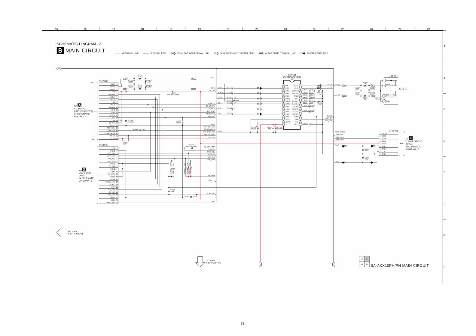
83
15 16 17 18 19 20 21 22 23 24 25 26 27 28
A
C
D
B
E
G
H
F
B MAIN CIRCUIT
SCHEMATIC DIAGRAM - 3
SA-AKX10PH/PN MAIN CIRCUIT
2/4
4/4
1/4
3/4
P1
P1
AA
: CD AUDIO INPUT SIGNAL LINE : AUX AUDIO INPUT SIGNAL LINE : AM/FM SIGNAL LINE: AUDIO OUTPUT SIGNAL LINE: -B SIGNAL LINE: +B SIGNAL LINE
ATOCD SERVO
CIRCUIT (CN7002)
IN SCHEMATIC
DIAGRAM - 1
FTOTUNER CIRCUIT
(CN51)
IN SCHEMATIC
DIAGRAM - 7
1
22
1
9
C2115 10
C2114 1
16V10C2129
16V220C2128
0.01C2127
1C2108
C2123
C2124
0.15
C2121 50V2.2
C2122 0.22
C2126 50V2.2
0.22
2.7KR2113
2.7KR2114
3300PC2120
C2125 3300P
C2119 0.22
C2118 0.15
IC2101C1BB00001151
ASP
C2113 1
10C2107
50V4.7C2817
C2109 1
CD-L
TU-L
AGND
TU-R
AUX-R
AUX-L
CD-R
ASP_CLK
ASP_DA
DGND
AGND SDA
SCLREFIN
VCC CEXT
LOUT LOUT
TREL
TRER
ROUTROUT
DGND
IGOUTRINL4
INL3
BASSL2
BASSR2
BASSL1
BASSR1
VOLINR
INR4
INR1
INR3
INR2
INL5
INR5
DIFFG
DIFFL
DIFFR
VOLINL
INL1
INL2
14
15
16
10
11
4
1
3
2
9
5
7
8
6
13
12
19
18
17
23
22
29
32
30
31
24
28
26
25
27
20
21IGOUTL
D2709B0ACCK000012
USB+5V
DC_DET_AMP
USB_SCL
C20080.1
1000PC2144 R2102
3.3K
R21013.3K
1000PC2143
CD_RST
R2009 3.3K CD_LOADING
1000PC2005
CD_BLKCK
CD_STAT
CD_OPEN_SW
CD_REST_SW
CD_MCLK
CD_MDATA
G0C470JA0055L2140
C21456.3V220
R21086.8K
R21056.8K
CD_MLD
6
5
8
9
11
12
10
18
15
17
16
20
19
13
14
7
2
1
4
3
22
21
CN2706
TUN_SDIO
1
2
3
4
JK2801
C20010
1000PC2003
1000PC2002
R200547K
R200647K
C2004100P
C2007100P
TUN_RST
TUN_GP102
TUN_SCLK
C21010.01
0.01C2102
CD-L
CD-R
TU-R
TU-L
AUX-R
AUX-L
3
2
6
7
4
5
1
9
8
CN2705
2
1
3
CN2704
GND
CD+7.5V
MOTOR_GND
CD3.3V
D5V
DGND
TX
RST
MLD
LCH
GND
RCH
GND
+3.3V
REST
SDIO
SCLK
GP102
PGND
ROUT
3.3V
3.3V
+7.5V
AGND
BLCK
LOUT
DGND
MCLK
STAT
BLKCK
LRCLK
LD_SW
MDATA
SRDATA
USB_SCL
AUX IN
[LCH]
[RCH]
GND
LOADING
REST_SW
CD_OPEN SW
TO MAINSECTION (1/4)
TO MAINSECTION (4/4)
GTOUSB CIRCUIT
(P901)
IN SCHEMATIC
DIAGRAM - 8
C2
81
91
00
P
C2
82
01
00
P
R2
80
51
0K
DVREF+
R2
81
24
.7K
R2
80
94
.7K
USB_IRQ
USB_VE
USB_TE
USB_SDA
ME
USB_RST
C2818100P
R2802 100K
6
5
8
9
11
12
10
18
15
17
16
20
19
13
14
7
4
22
21D3.3V
Mmodo.error
DGND
CD_DATA
DGND
CD_CLK
DGND
USB_SDA
USB_IRQ
Verify.error
CD_STAT
CD_MLD
DGND
CD_RST
USB_RST
STCLK
STIN
STREQ
Timeout.error

84
I
8 9 10 11 12 13 14
K
L
J
B MAIN CIRCUIT
SCHEMATIC DIAGRAM - 4
SA-AKX10PH/PN MAIN CIRCUIT
2/4
4/4
1/4
3/4
TO MAINSECTION (4/4)
TO MAINSECTION (1/4)
1
P1
: CD AUDIO INPUT SIGNAL LINE : AUX AUDIO INPUT SIGNAL LINE : AM/FM SIGNAL LINE: AUDIO OUTPUT SIGNAL LINE: -B SIGNAL LINE: +B SIGNAL LINE
HTOD-AMP CIRCUIT
(CN5902)
IN SCHEMATIC
DIAGRAM - 9
1
12
C22250.18
C22200.22
C22240.22
R22252.7K
2.7KR2229
C22210.18
B1ABCF000176Q2222
C222610
C222210
R22281K
R2227100K
R22241K
R2223100K
Q2223B1ABCF000176
SWITCH
Q2221B1ABCF000176
SWITCH
Q2220B1ABCF000176
AMP
AMP
R22224.7K
R22264.7K
R223056K
R223156K
R22065.6K
R22055.6K
C220447P
R23102.2K
R23092.2K
R2313100K
R2314100K
R23121K
Q2302B1ABCF000176
SWITCH
R23072.2K
R23082.2K
C230110
C230210
0R2203
1KR2201
1KR2202
0R2204
10V100C2201
R220827K
C222316V100
R22202.2K
R22214.7K
C240510
C22031
C240210
C22021
C23090.015
C23100.015
27KR2207
C2206
VCC
GND
560P
47PC2205
6 75
24 3
8
1
IC2201C0AABB000125
OP-AMP
560PC2207
C23070.1
C23080.1
100R2303
100R2304
330R2305
330R2306
USB+5V
B0ACCK000012D2790
B1ABCF000176SWITCH
Q2790 PCONT2.2K
R2791
2.2KR2790
MUTE_F
AGND
FRONTR
FRONTL
LOUT
ROUT
0K2706
7
9
10
8
4
5
1
3
2
6
12
11
CN2711
F_HOP2
F_HOP1
MUTE_F
DC_DET_AMP
MOD_DA
USB+5V
GND
FRONT R
FHOP2
FHOP1
AGND
FRONTL
FRONTR
FRONTL
SIGNAL A_GND
MUTE F_SW (MODE 2)
+5V GND
+5V
MOD_DA
DC_DET1
ECO / FAN
1 2 3 4 5 6 7
M
O
P
N
B1ABCF000176SWITCH
Q2301
R260222K
D2602B0ACCK000012
R23111K
B0A
CC
K000012
D2603
C260150V2.2
R2605100K
R26014.7M
R260622K
R260422K
C26030.012
C260250V1
R261122K
D2605B0ACCK000012
B0A
CC
K000012
D2604
C260850V2.2
R2608100K
C26050.012
C260750V1
CLIP_S
CLIP_ATTN

85
I
K
L
J
M
O
P
N
22 23 24 25 26 27 28
B MAIN CIRCUIT
SCHEMATIC DIAGRAM - 5
SA-AKX10PH/PN MAIN CIRCUIT
2/4
4/4
1/4
3/4
TO MAINSECTION (2/4)
1
AA
P1
P1
: CD AUDIO INPUT SIGNAL LINE : AUX AUDIO INPUT SIGNAL LINE : AM/FM SIGNAL LINE: AUDIO OUTPUT SIGNAL LINE: -B SIGNAL LINE: +B SIGNAL LINE
ITOSMPS CIRCUIT
(CN5802)
IN SCHEMATIC
DIAGRAM - 10
17
B0BC8R2A0266D2704
B1BACG000023REGULATOR
Q2701
C270410V33
C27020.1
C27110.01
R2701100
D2708B0EAKM000117
D2707B0EAKM000117
D2706B0EAKM000117
D2120B0EAKM000117
390R2702
C27060.01
16V47C2712
16V47C2708 C2717
25V330
2 13
IC2701C0CAAKG00046VOLTAGE REGULATOR
C27160.01
G2G1
ZA2701*
C270516V47 4.7K
R2705
1KR2704
721 270
719 2.2
718 2.2
720 2.2
C27070.01
720 0.01
CE0000122705
00019ONTROL
21M
R2710
G0A101ZA0028L2702
E2701
6
8
9
7
2
1
4
5
3
10
11
ZJ2701*
1 32
4 2 135
C0DAAYG00001SWITCHING REGULATOR
IC2702
0.01C2713
0.01C2719
B0JC
PD
000025
DZ
2701
0.47C2714
C27156.3V820 25V330
C2718
QR2704B1GBCFJJ0051
ENT LIMITERDC DETECT
R27082.7K
1.5KR2706
1KR2707
B1GBCFJJ0051QR2702
QR2701
R277422K
3
1
2
D2711B0ADCJ000020
B1GBCFJJ0051
DC DETECT
DC DETECT
AM_BP
PCONT
15KR2773
SYS3.3V
SYNC
CD+7.5V
MOTOR_GND
NC
SYS3.3V
NC
PCONT
DC18V
+18V.-12V_GND
DCDET2
SYNC
+18V.-12V_GND
AM_BP
DC18V
GN
D
VC
C
OU
T
INV
IN
ST
BY
GNDOUT
R277212K
2
1
4
3
CN2709NC
NC
DC 18V
FL-GND
15 16 17 18 19 20 21
TO MAINSECTION (3/4)
CTOPANEL CIRCUIT
(CN6002)
IN SCHEMATIC
DIAGRAM - 6
1
C270316V47
C21466.3V220
C27010.01
R2
R2
R2
R2
C2
B1ADQ
B1AAJC0CURRENT C
Q270
CURR
USB+5V
DC_DET_PWR
D2710B0ACCK000012
G0A220GA0002L2801
DGND
GND
AGND
FL_CLK
FL_CS
V_JOG_A
KEY1
ROTARY_JOG
KEY2
RMT
DVREF+
FL_DA
VREF+6
5
8
9
11
12
10
14
15
13
7
17
16
KEY2
VP DET
FL_CS
DGND
DVREF+
KEY1
RMT
J_VOLA
FL_DOUT
FLCLK
CD3.3VCD3.3V
VREF+
ROTARY JOG

86
18.3. Panel Circuit
A
1 2 3 4 5 6 7 8 9 10 11 12 13 14
8 9 10 11 12 13 14
C
D
B
A
C
D
B
E
G
H
F
C PANEL CIRCUIT
SCHEMATIC DIAGRAM - 6
SA-AKX10PH/PN PANEL CIRCUIT
: -B SIGNAL LINE: +B SIGNAL LINE
BTOMAIN CIRCUIT
(CN2709)
IN SCHEMATIC
DIAGRAM - 5
DTOCD OPEN BUTTON
CIRCUIT (ZJ6001B*)
IN SCHEMATIC
1
17
6.8KR6105
C610450V47
KEY2
10KR6013
10KR6012
KEY1
D6101B0BC024A0269
50V47C6102R6101
47K
D6104B0EAMM000057
R602522K
R602110
B0BC2R4A0263D6001
L6101G0A220GA0002
L6001J0JBC0000019
50V22C6014
R6108 1
SG
4
SG
2
SG
1
SG
3
SG
14
SG
13
SG
15
SG
7
SG
9
SG
10
SG
8
SG
5
SG
6
SG
12
SG
11
C60130.1
R610247
D6102B0JAME000114
R60093.3K
GR
2
GR
1
GR
5
GR
10
GR
11
GR
8
GR
9
GR
12
GR
6
GR
7
GR
3
GR
4
S6009
R60043.3K
S6004
SG
16
1
2
ZJ6001A*
S6005
S6012
S6011
SG11
SG10
SG14
SG16
SG15
SG13
GR11
GR10
GR12
SG12
1
2
35374244 43 39 3841 40 36
33
31
29
27
24
23
26
25
28
30
32
346.8K
R6005
C60030.1
R60104.7K
GR
5
GR
4
GR
8
GR
9
GR
6
GR
7
GR
1
GR
3
GR
2
S6010
R60061.2K
D6105B0BC036A0264B0EAMM000057
D6103
S6006
S6007
R60082.2K
R60071.5K
0R6103
R6106 1
C610116V100
5 3
4
8
7
6 2
1
9T6101G4DYA0000214
SWITCHING TRANSFORMER
435 62 3 41 8 39353127 2825 26 3029 3432 33 3836 37 4240 411312 15 16149 1110 23 2418 1917 21 22207 44
FL6001A2BB00000171
FL DISPLAY
S6008
S6002
S6001
S6003
1.2KR6001
R60021.5K
R60032.2K
C61033300P
Q6101B1BABK000001
POWER SAVE CONTROL
P0
FM/AM
6
5
8
9
11
12
10
14
15
13
7
2
1
4
3
17
16
CN6002
KEY2
RMT
J_VOLA
KEY1
FL_CLK
DGND
VREF+
DVREF+
ROTARY_JOG
FL_DOUT
FL_CS
RMT
KEY2
NC
NC
DGND
FL_CS
DVREF+
J_VOLA
VREF+
CD3.3V
DC 18V
VP DET
FL_GND
FL_CLK
FL_DOUT
ROTARY JOG
KEY1
CD PLAY/PAUSED.BASS
MANUAL EQ
REWIND
FORWARD
ALBUM -
ALBUM +
POWER
USBPLAY/PAUSE
AUX
STOP/-DEMO
P1
G2
G4
G3
VD
D
G1
5
4
E
7
6
3
G6
G8
G7
G5
G9
G11KEY2
DGND
0
2
1
1 2 3 4 5 6 7
E
G
H
F
ETOREMOTE SENSOR
CIRCUIT (CN6301)
IN SCHEMATIC
DIAGRAM - 7
DIAGRAM - 7
DGND
C60101000P
R602012K
R601810K
VR6001EVEKE2F3524BVOLUME JOG
C6009100P
C6008100P
R601922K
J_VOLA
DVREF+
R602322K
R602410K
ROTARY_JOG
K9AA012Y0004TRACK JOG
VR6002
C6012100P
C6011100P
12KR6022
SG
2
SG
1
SG
8
SG
6
SG
7
SG
9
SG
4
SG
3
SG
5
R6017 82K
0.01C6007
330P
C6004
330P
C6006
330P
C6005
RMT
VREF+
21
5
6
3
4
19
9
7
8
16 17
11
10
12 151413 18 20 22
C0HBB0000061FL DISPLAY DRIVER
IC6001
FL_CLK
FL_CS
220R6014FL_DOUT
R6015 220
R6016 470
2
1
4
3
CN6001DIN
OSC
P3 [44] VSS
P2
NC S1
S1
VE
G12/S1
S1
S1
[33] G10
[12] VSS
NC
DGND
RMT
VREF+K1
K2
CLK
STB
S7
S6
S5
S8 S1
[22] S9
S1
S2
S4
S3
VD
D
S1
S1
1
2
3
1 2 3
R6028 1K

87
18.4. CD Open Button, Remote Sensor & Tuner Circuit
A
1 2 3 4 5 6 7 8 9 10 11 12 13 14
8 9 10 11 12 13 14
C
D
B
A
C
D
B
E
G
H
F
D CD OPEN BUTTON CIRCUIT
F TUNER CIRCUIT
E REMOTE SENSOR CIRCUIT
SCHEMATIC DIAGRAM - 7
SA-AKX10PH/PN CD OPEN BUTTON / REMOTE SENSOR / TUNER CIRCUIT
: +B SIGNAL LINE
: +B SIGNAL LINE : AM SIGNAL LINE : AM/FM SIGNAL LINE: FM SIGNAL LINE
CTOPANEL CIRCUIT
(ZJ6001A*)
IN SCHEMATIC
DIAGRAM - 6
CTOPANEL CIRCUIT
(CN6001)
IN SCHEMATIC
DIAGRAM - 6
BTOMAIN CIRCUIT
(CN2705)
IN SCHEMATIC
DIAGRAM - 3
1
9
R62014.7K
S6201
1
2
ZJ6001B*
OPEN/CLOSEKEY2
DGND2
1
4
3
CN6301
C6301100P 1000P
C6302
1
2
3B3RAB0000084
REMOTE CONTROL SENSOR
Z630150V22C6303RMT
DGND
VREF+
NC
3
2
6
7
4
5
1
9
8
CN51
3.3V
GND
GND
R OUT
L OUT
RST
INT
SCLK
SDIO
1 2 3 4 5 6 7
E
G
H
F
AM ANT4
G2
G1
6
2
3
1
0.1C61
R521K
C59 1 R51
1K
X51
H0A
32
72
00
09
7
R59 2.2K
C60 1
22PC58
22PC57
R62
47K
R61
47K
R55 220
R57 1K
R56 220
R544.7K
LB51J0JBC0000032
L51C511000P
G2
G3
G1
JK51
VA51EZAEG2A50AX
R640
214
1
2 14
T1 17 16
15
20
313Thermal
Pad
115
1076
IC52
1
2
JK52
0.1C62
R534.7KC52
L52
SE
N
SC
LK
RFGND
AM ANT
AM ANT
GNDRST
G2A380Y00001
0.47
AMI
GC
GP
O1
NC
NC
FM ANTFMI
FM/AM RADIO RECEIVER
VDD
VIO
SD
IO
DC
LK
ROUT
DOUT
DF
S
LOUT
RC
LK
GND
GC
GP
O2
G1CR18JA0020
VUEALLPT031 19 18
8 9
FM ANT

88
18.5. USB Circuit
A
1 2 3 4 5 6 7 8 9 10 11 12 13 14
8 9 10 11 12 13 14
C
D
B
A
C
D
B
E
G
H
F
G USB CIRCUIT
SCHEMATIC DIAGRAM - 8
SA-AKX10PH/PN USB CIRCUIT
: USB SIGNAL LINE: +B SIGNAL LINE
BTOMAIN CIRCUIT
(CN2704)
IN SCHEMATIC
DIAGRAM - 3
L900G1C100K00019
0.1
C902
2.2KR957
0R950
R972 1K
R971 1K
C9140.1
C907 18P
R9140
C908 22P1KR901
X900H0A120500009
0R904
1KR902
15K
R955
LB9510
C953
6.3
V100
15K
R954
24R953
R952 242
5
G1
4
6
G
3
P903
USB PORT
LB9520
16V
10
C931
0.1
C952 0
.1C
951
R958100K
R9030
LB8520
6
5
8
9
11
12
10
18
15
17
16
20
19
13
14
7
2
1
4
3
22
21
P901
0R907
0.1C911
0.1C912
23303132
40
41
35
37
36
33
34
39
38
42
28 2526 242729 19 1820
8
7
15
16
9
13
10
12
11
14
1722 21
MNZSFB5KJM2USB CONTROLLER
IC900
DGND
P01
P04
P02
P03
P81/D8
P73/D
5
P70/D
2
P00
P66/D
0
P72/D
4
P71/D
3
P75/D7
VSS
VDDI
VDD33
P82/D9
P85/D12
P86/D13
P83/D10
P84/D11
P67/D
1
US
B_C
TR
L
VP
P
OC
D_S
DA
VDDI
OSCI
VSS
NRST
AVDD
VDD33
OSCO
MMOD0
CD_NRST
MMOD1OC
D_S
CL
US
B_
PO
WE
R
DGND
VBUS
D+
D-
VSS
DGND
DGND
TERR
STREQ
CD_MLD
MMOD
DGND
D3.3V
M_NRST
CD_NRST
STIN
DGND DGND
DGND
VERR
I2C_REQ
DGND
DGND
DGND
CD_STAT
STCLK
CD_DATA
CD_CLK
I2C_DATA
D5V
DGND
I2C_CLK
DGND
1 2 3 4 5 6 7
E
G
H
F
C904
16V
10
0.1
C905
10
C906 0
.1C
901
47
C915
C903
0.1
0R906
58
45
44
47
48
46
43
55 5650 5149 53 5452 57 62 6361
3
2
5
4
6
1
6459 60
0.1
C913
DGNDP77/NRE
I2C_CLK/WR_END
I2C_DATA/ERROR
I2C_REQ/WR_START
P40/D15
P87/D14
VSS
USBNOC
USBNPP
USBD+
USBD-
PD6/IRQ3
VD
DI
PA
7
VS
S
VE
RR
TE
RR
VD
D5
ST
IN
DGND
CD
_M
LD
ST
RE
Q
P21/N
CE
0
ST
CLK
CD
_D
AT
A
CD
_C
LK
CD
_S
TA
T
PD
4/N
CE
2
P91/S
BIO

89
18.6. D-Amp Circuit
A
1 2 3 4 5 6 7 8 9 10 11 12 13 14
8 9 10 11 12 13 14
C
D
B
A
C
D
B
E
G
H
F
H D-AMP CIRCUIT
SCHEMATIC DIAGRAM - 9
SA-AKX10PH/PN D-AMP CIRCUIT
: AUDIO OUTPUT SIGNAL LINE: -B SIGNAL LINE: +B SIGNAL LINE
TO SPEAKERS
ITOSMPS CIRCUIT
(CN5801)
IN SCHEMATIC
DIAGRAM - 10
C59330.015
TH5900D4CC11040013
R5926
100
0.4
7C
5941220P
C5934
C5932
0.1
C5937
0.1
0.1
C5936
220PC5935R5922
10
C5930
0.4
70.1
C5931
R5924
5.6
K
C59380.1
C59390.1
C59471000P
0.1
C5952
C5953
0.1
C5955
0.1
C5954
0.1
2
43
1
L5905G0B9R5K00005
5.6KR5933
0.68C5949
D5906B0HCSP000001
D5905B0HCSP000001
R593222
5.6KR5934
0.1C5951
4
2
3
1
FR-
FL-
G2
FL+
G1
FR+
JK5901
2
43
1
L5904G0B9R5K00005B0HCSP000001
D5904
B0HCSP000001D5903
C59500.1
R593122
C59480.68
2
43
1
G0A150L00003L5903
C59421000P
C594616V10
C5944
0.4
7
C5943330P
R5925
5.6
K
19 21 2322201021 8 974 5 63 12 1514 17 18161311
C1BA00000497POWER AMPLIFIER
IC5900
10R5921
C5925
C5926
0.1
0.1
C59171000P
C5920100V22
10
R5917
C5915
0.4
7
0.4
7C
5919
220PC5929
220PC5927
C5918330P
R5914
5.6
K
R5911
5.6
K
C59280.015
C59210.1
C592433P
C59230.1
R59236.8K
R592882KF000176
906
82KR5927
10V100C5945
F000176
ETECT
ETECT
907
10R5905
0C5956 GND
0.1C5904
0.1C5903
2
4
3
1
6
5
ZJ5901*
L5902J0JKB0000020
50V220C5908
C59090.1
C59100.1
50V220C5907
L5901J0JKB0000020
C59050.1
0.1C5906
MO
DE
IN2+
VS
SP
2
PR
OT
OU
T1
VD
DP
1
BO
OT
1
SG
ND
1
VD
DA
1
VS
SA
1
OS
C
ST
AB
I
VS
SP
1
VS
SD
OU
T2
SG
ND
2
VS
SA
2
VD
DA
2
BO
OT
2
VD
DP
2
IN1-
IN1+
IN2-
GND
VDD
VDD
VSS
GND
VSS
1 2 3 4 5 6 7
E
G
H
F
BTOMAIN CIRCUIT
(CN2711)
IN SCHEMATIC
DIAGRAM - 4
12
1
R59182.7K
R59132.7K
Q5905B1ABCF000176
SWITCH
B1ABCQ5
R591510K
B1ABC
DC D
DC D
Q5
R5901120K
B1GBCFJJ0051SWITCH
QR5900
R593510K
R590410K
C59021000P
C59011000P
7
9
10
8
4
5
1
3
2
6
12
11
CN5902
B1GDCFJJ0047SWITCH
QR5901
B1ADCE000012SWITCH
Q5902
R59101.5K
R590933K
R5906180K
Q5901B1ABGC000005
SWITCH
R590727K
R590310K
R590810K
Q5903B1ABCF000176
SWITCH
SGND
FL_IN
FHOP1
+5V
FHOP2
AGND
MUTE_F
DC_DET
MOD_DA
ECO / FAN
+5V GND
FR_IN

90
18.7. SMPS Circuit
A
1 2 3 4 5 6 7 8 9 10 11 12 13 14
8 9 10 11 12 13 14
C
D
B
I SMPS CIRCUIT
SCHEMATIC DIAGRAM - 10
SA-AKX10PH/PN SMPS CIRCUIT2/21/2
TO SMPSSECTION (2/2)
P1
1
2
3
4
HTOD-AMP CIRCUIT
(ZJ5901*)
IN SCHEMATIC
DIAGRAM - 9
: +B SIGNAL LINE : -B SIGNAL LINE
2
3
1
C5HACYY00004...PNIC5701
C5HACYY00005...PHSWITCHING REGULATOR
31 2
B0ABSM000008D5801
R5832 R5833
18KR5863
18KR5862
4.7KR5861
R5800
R586010K
R586410K
0.1C5831
0.1C5832
3
4
1
2
6
5
CN5801
B1ADCF000001Q5860
100K...PH33K...PN
R5702100K...PH33K...PN
R5703
50V1000C5805
V10005808
RJ0000125803
22R5720
D5731B0EAMM000057
3
21
D5702
B0ZAZ0000052
C57130.01
ETS39AG4NGAD...PNETS39AG4M6AD...PH
FOR PN FOR PH
MAIN TRANSFORMER
C5821
0.0
1C
5819
0.0
1
C5822
0.0
1C
5820
0.0
1
A
R
3
2
C1
0DABFC00002SHUNT REGULATOR
VERTER
CURRENTLIMITING SWITCH
CURRENTLIMITING SWITCH
FEED BACK
IC5801
CFLL0037R5810
330R5809
330R5807
1KR5730
B0BC6R100010D5725
2.2KR5808
4
3
1
2
B3PBA0000402PC5720
FEED BACKB3PBA0000402
PC5701
R5810330
R5817330
4
3
1
2
120R5724
11
13
14
12
10
8
6
5
7
9
18
15
16
17
1
4
3
2
T5701
C581335V330
R57221.2K
C57221000P
C5721220P
R5729
10K
R5728
100K
C57281000P
D5724
D5727
B0ACCK000012
B0ACCK000012
R5732100
R57260.1...PH0.15...PN
B1ABCF000176Q5722
10KR5721
D5722B0BC019A0007
B0ACCK000012D5723
C57200.1
B0BC018A0267...PNB0BC010A0007...PH
D5721
J0JBC0000019L5704
D5726B0EAKM000117
D5729B0EAMM000057
SWITCH
1KR5723
B1ADCF000001Q5721
B0ACCK000012D5728
B1BABG000007Q5720
DC5737...PH820P
C5727...PN3300P
C57260.1
C57301
C5724
D5732
B0B
C035A
0007
50V56R5733
47K
C57250.1
C5723470P
S
GND
FB
VCC
OLP/SS
OCP/BD
+30V_SENSE
GND
GND
-30V_SENSE
-30V_SENSE
+30V_SENSE
4
5
7
6
TRANSFORMERTEMP DETECT.
B1GBCFJJ0051Q5862
TRANSFORMERTEMP. DETECT
B1ABCF000176Q5861
TRANSFORMERTEMP. DETECT
C58690.1
C58700.1
TH5860D4CC11040013
11
13
14
12
10
8
6
5
7
9
18
15
16
17
1
4
3
2
VIN
VCC VCC
DRAIN
VIN
DRAIN
+30V
-30V
+FAN 18V
+30V
+FAN 18V
GND
+18V
GND
+18V
AMPGND
-30V
AMPGND
11
13
14
12
10
8
6
5
7
9
18
15
16
17
1
4
3
2
R5841
FOR PN
R5727 0.13
R5836
1 2 3 4 5 6 7
E
G
H
F
BTOMAIN CIRCUIT
(ZJ2701*)
IN SCHEMATIC
DIAGRAM - 5
R58342.2K
2.2K 2.2K
B1GBCFJN0038QR5801
R580122K
D5804
15K
C5800
GND
0.01C58260.01
50C
B0HFD
SYNC
SYS3.3
2.2KR5805
15KR5806
C
IN
0.1C5818
0.1C5812
1KR5803
100V0.1C5817
47KR5804
8.2KR5814
0.1C5810
12KR5802
C58960.1
5
7
8
6
2
1
4
3
9
11
CN5802
PCONT
B1GBQ
3 12
B0ABSM000008D5802
PCONT
DC18V
AM_BP
10NC
DCDET
DC18V
+18V.-12V_GND
+18V.-12V_GND
SYS3.3
SYNC
NC
POWER CONTROL
C584410
C584310
PCONT
AM_BP
Q5803B1BABG000007
AMBP SWITCH
AM_BP
R582010K
B0ACCK000012B1GDCFGA0018
QR5802
120K
R584082K
DC DETECT
2.2KR5835
FOR PH
470R5828
470R5824
470R5827
470R5823
470R5826
470R5822
470R5825
470R5821
R58372.2K
2.2K
K1...PN0
K3...PH0

91
15 16 17 18 19 20 21 22 23 24 25 26 27 28
22 23 24 25 26 27 28
A
C
D
B
E
G
H
F
I SMPS CIRCUIT
SCHEMATIC DIAGRAM - 11
SA-AKX10PH/PN SMPS CIRCUIT2/21/2
TO SMPSSECTION (1/2)
P1
3
JTOVOLTAGE SELECTOR
CIRCUIT
IN SCHEMATIC
DIAGRAM - 12
: +B SIGNAL LINE : -B SIGNAL LINE
400V220...PH200V560...PN
C5712
6
7
5
2
4
3
8 1
IC5799MIP2F20MSSCF
F0CAF224A105...PNF0CAF104A105...PHC5703
0.1...PH0.22...PN
3
2
1
4
B0FBAR000043D5701
SYNC
D5730MA2YF8000L
R5706820K
D5798B0EAMM000057
220KR5704
220KR5705
R579822
C579825V220
4
3
1
2
PC5702B3PBA0000402
4
3
1
2
B3PBA0000402PC5799
100R5897
Q5898B1ABCF000176
R5896100K
C58970.1
2.2KR5890
150R5894
B0HAMP000094D5793
C57902200P
200KR5786
SWITCHING POWERSUPPLY CONTROL
SWITCH
SYNC SWITCH
FEED BACK
FB
S
S
D
NC
VDD
CL
VCC
(RED)TL8*
(BLK)TL7*
FOR PH
FOR PN
FOR PH
FOR PH
FOR PH
C5711400V220
C57951
15KR5797
R5795470K1000P
C5794
B0BC9R000008D5795
0.1C5796
C5705F1BAF1020020
1000P
C5704F1BAF1020020
1000P
GND
C5706F1BAF1020020
1000P
GND
C5707F1BAF1020020
1000P
ERZV10V511CS120V 60Hz...PN110V~127V/220V~240V 50Hz/60Hz...PH
AC IN
2
3 4
1
L5703G0B612H00002
1.5MR5708
1.5MR5709DZ5701
C5701
0.33F0CAF334A105
ZA5701
P5701
ZA5702
8A 125V...PNT6.3AL 250V...PH
F1
TH5702D4CAA2R20001
15 16 17 18 19 20 21
1
2
4
SYS3.3
10KR5893
C589910V220IC5899
C0DAEMZ00001
B0EAMM000057D5896
R589133K
9
10
7
8
1
6
ETS19AB2E6AGSUB TRANSFORMER
T5751
1KR5892
15KR5895
0.1C5898
A
R
1
3
C
2
5
4
2
3
SHUNT REGULATOR
C5708F1BAF1020020
1000P
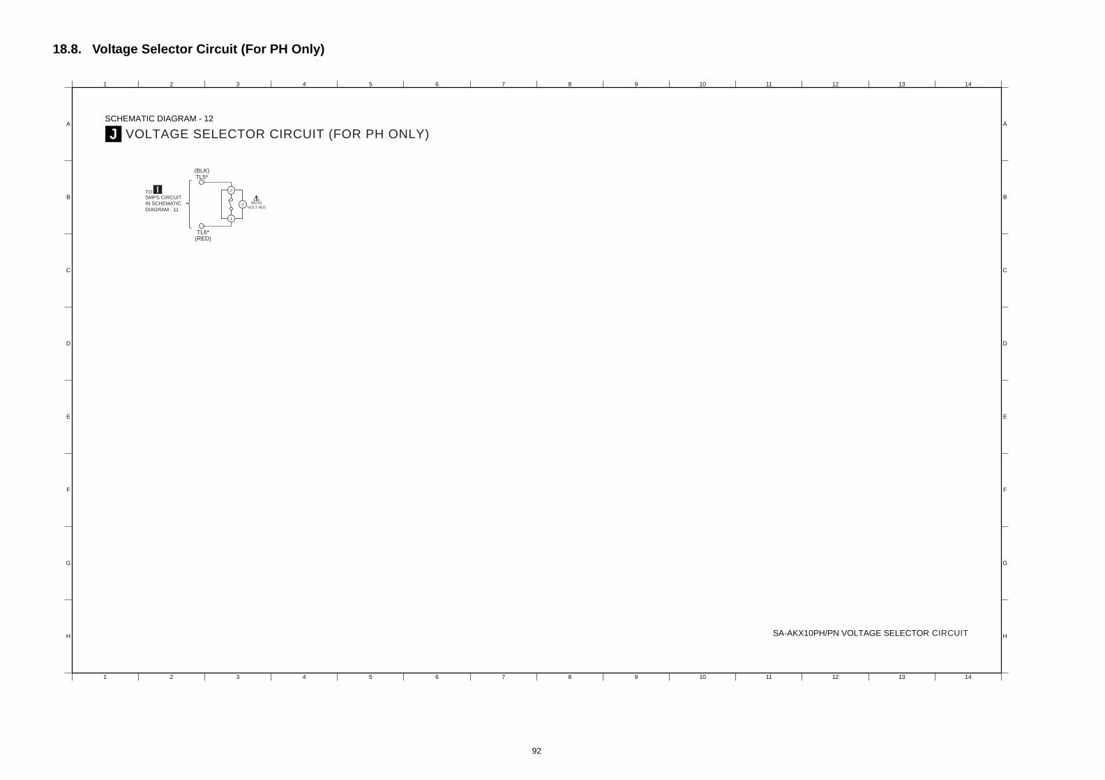
92
18.8. Voltage Selector Circuit (For PH Only)
A
1 2 3 4 5 6 7 8 9 10 11 12 13 14
8 9 10 11 12 13 14
C
D
B
A
C
D
B
E
G
H
F
J VOLTAGE SELECTOR CIRCUIT (FOR PH ONLY)
SCHEMATIC DIAGRAM - 12
SA-AKX10PH/PN VOLTAGE SELECTOR CIRCUIT
ITOSMPS CIRCUIT
IN SCHEMATIC
DIAGRAM - 11
(BLK)TL5*
TL6*(RED)
S5701
VOLT ADJ
2
3
1
1 2 3 4 5 6 7
E
G
H
F

93
19 Printed Circuit Board19.1. CD Servo, Tuner & Voltage Selector P.C.B.
17 8 9
F
G
H
10 1 12 13
A CD SERVO P.C.B. (REPX0636A) F TUNER P.C.B. (REP4557A)
SA-AKX10PH/PNCD SERVO / TUNER / VOLTAGE SELECTOR P.C.B.
(SIDE A) (SIDE B)
J VOLTAGE SELECTOR P.C.B. (REPX0809C...PH)
0688CB0688CB
R76
01 C76
70
C76
01
W7002C7102
TP51(ARF)
C71
61
C72
23C
7203
R72
11
C72
17
C72
41
C72
18
C7244
C7216 R7212 R7217
C7230
(TRV MOTOR)M7301*
C7231
C7227TP19
TP18
TP16
TP39
R72
21
C72
63C7234
C7235
X7201
R7220C72
64
221
CN7001
IC7001
W7013
C7613
C71
55
C71
54
W70
08W
7007
W70
06
W70
10
W70
11R
7111
W70
12
W7009
C7626
TP88
TP89
W7015
TP86
TP87TP28
(VREF)
C71
64
C71
65
R72
53C71
66
W70
2472
32
C72
22
7214
LB7262
TP17
TP24
TP7
TP13
TP12
LB7263
W70
16LB7264
CN7002C
7228
TP38
W70
21
C72
25C
7226
R7218
C72
04
TP50
W7003W7004W7005
W70
01
D76
50
C71
07
C71
42
TP14
L52
C59
L51
JK52JK51
CN51
C51
LB51
R51
X51
C52
R61
VA51
C58
C62
R57
R64
C61
R55R54R56R53IC52
R62
R52
C60
C57
R59
S5701
VOLT ADJ
RED BLKTL6*TL5*
(VOLTAGE SELECTOR)
PbF
321
1 2 3 4 5 6
A
B
C
D
E
NOTE: " * " REF IS FOR INDICATION ONLY.
C7315
TP37
(REST SW)
C7
R73
15
R73
25
R73
23R
7331
C73
38
R7329
TP90
C73
52
R73
36
C76
14
R7327C7339
Q7601 R7330
R73
49
R73
39
R73
28
W70
14R
7650
R73
35
R73
32
C
C72
33
R72
54
R
TP8TP9
TP4TP31
W7017
C7335IC7002
S7202
M7302*C7334
W70
25
C72
53C
7243
W70
18
W70
19
W70
26
W70
20
TP36
(CD OPEN SW)
(SPL MOTOR)
TP10
TP11
TP3TP1TP2
S7201

94
19.2. Main P.C.B.
17 8 9
E
F
G
H
10 1 12 13
B MAIN P.C.B. (REPX0814BA...PH)(REPX0814AA...PN)
SA-AKX10PH/PNMAIN P.C.B.
0668AA0668AAPbF
R21
01
R2105
802
D2711
Q2790
QR2701
QR2702
DZ
2701
D2790
D27
04
D27
10
R2701
C27
02
C2719
C2713
714
C27
11C2706C
2716
R2702
R2707
708
R27
10
R27
72R
2773
R2790
R2791
R2774
R28
86
R28
85
884
R2882
R2881
R2887
R2888
R28
56
R28
57
R2859
R2865R2867R2868
R2870R2872
R2873
R2877
R2878
R2879
C2805 R2883
C2807
QR2801
D2803
QR2802
R28
91
R2889
R2893
C21
43
C21
02
C21
01R2006
C2004
R2005
C2001
C20
03 C2007
C20
02
C2108
C21
09
C21
13
C2119
R21
14
C2123
C2125
C21
27
C22
02
C22
03
R2206
C21
14
R21
13
C2120
C2122
R2201
R22
02
R22
03
R2204
R22
07
C22
06C
2204
R2205
R22
08
C22
07C
2205
R26
04
Q2301 Q2302
R23
11
R23
09
R23
12
R23
10
R2308
R2307
R2305
C2307 R2303
C2402
C2405
D26
03
W2503
C2118
C2124
R2314 R2313
R27
19
R27
18
QR2704
R2721
R2890
C2811
C2816
D28
04
W2504
R26
06
IC2101
QR2831
QR2832
R22
20
R2221
R2226
R22
27
R22
29
R2222
R22
23
R2224
R22
25
R2231
R2230
C2224
C22
25 C2220
C22
21
Q2222
Q2223
Q2220 Q2221
W25
08
C2301
C2302
W25
01
W2515
W25
02
C21
07
C2115
K27
06
R26
08
R2611
C22
22
C2309
C23
10
C26
05
D26
04
D26
05
CN2706
C2712
IC2701
IC2702
L270
2C
2718
C2708
C27
04
D27
06 D2707
D2708
W20
02
W20
05
C27
17
W20
23
K27
04
C28
10
Q2803
W21
03
W20
25
W20
24
W20
38
W20
37
CN2705
IC2201
JK2801
C2201
C26
02
W2035
W20
08
W2036
W20
16
W20
15
W2101
W20
14
W20
13
W20
09
W20
20
W20
19
W20
18
W2032
W2010
W2012
W21
02
W20
55
W2030
W20
34
W20
39
W2029
W20
43
W2011
W20
27 W20
31
W20
33
W20
58
W20
01
W20
41
W20
40
W20
21
W2047
W20
17W
2057
W20
07
W20
03
W20
04
W20
28
W20
26
W20
06
C2121
K2705
C21
26
C21
28C21
29
K27
02
K2703
223
CN2711
E2701
ZA2701*
W20
22
CN2709R
2607
C28
17
K20
01...
PN
K20
02...
PH
W25
17
W2518
Q2701
C2607
C2608
ZJ2701*
D21
20
K3902
AUX
J200
1
J2703
B C E
BCE
BC
E
BC
E
BC
E
BC
E
BC
E
BC
E
BC
E
CAA
CA
C
BC
E
BC
E
BC
E
BC
EB
BC
EB
CE
21
22
9
20
1
1
3
2
1
3
21
2
3
4
5
21
89
67
45
3
1
45
8
2-LCH
3-RCH
1-GND
4-GND
21
43
65
87
9
1112
10
12
34
56
7
98
1716
1514
1312
1110
12345678911 10
1 8
16
1
4
8
12
17
20
24
28
32
1 2 3 4 5 6
A
B
C
D
NOTE: " * " REF IS FOR INDICATION ONLY.
IC2801
R20
09
R21
02
R21
08
R28
10
D2709
R28
05
R28
09
R28
12
R2
R2704
C2
C2701
C2707
R2706
R2
R27
05
R28
28
R28
29
R28
30
R28
31
R28
16
R28
17 R28
15
R2822
R28
21 R2824
R28
34
R2
R2880
R28
71
R28
75R
2869
R2866
R2864
R28
63
R28
62
R28
60
R28
58
C2804
R28
74
R2836
R28
38
R28
42
R2849
R2851
R2852
R2854
R28
55
D2802
D28
01
R2825
R2826
R28
27
R2835
C28
03
R28
50R
2853
R28
48
R28
47
C28
01
C28
02
R2839
R2840
R2841
R28
43
R28
46
IC2802
W2505
W2511
C21
44
W2510
C2603
R26
02
R2601
C23
08
R2306R23
04
D2602
R2605
C2005
R27
20
Q2705
C20
08
W25
09
C2812
R2892
R28
94
W2507
C27
20
R2228
W2512
W2514
W25
13
R2130
C28
18C
2819
C28
20 W25
16
C2226
CN2704
C2715
Q2702
W2063
W20
61
X2802
X2801
W2059W20
89
C2806
W20
79
W21
05
W20
76
W20
94
W20
90
W20
84
W21
06
W20
86
W2044
W2045
W2046
W2073
W2050
C2601
W21
00
W2075
W20
82
W2074
W2052
W20
96
W20
80
W20
60
W2064
W20
97
W21
07
W2051
W2077
W2049
W2078W
2099
W20
85
W2095
W20
93
W2091
W2048
W21
04
W2069
W2065W
2092
W20
98
W20
88W20
62
W2068
W2067
W2066
W2072
W2071
W2070
W2042
W20
53
W2054
K2701
C2
CN2707
C2705
C2703
C2146
C2145
L2140
L280
1
(FOR DEBUG)
J205
1
J270
1
BCE
B
E
CE
2
1
2
3
2
5
2
7 9 117
18
15
16
13
14
11
1210
2
43
65
87
2122
1920
1718
1516
1314
1112
910
1
3
2
1
2
3
4
5
6
7
8
4 5
1
5
10
15
20
25
75
70
65
60
55
3031
35
40
45
95
90
85
50
51
80 81
100

95
19.3. Panel P.C.B.
17 8 9
E
F
G
H
10 1 12 13
C PANEL P.C.B. (REPX0814BB...PH)(REPX0814AB...PN)
SA-AKX10PH/PNPANEL P.C.B.
0668AB0668AB
R60
19R
6020
R60
18
C6010
R6023
R60
24
R60
22
C60
08C
6009
C6011
002
R60
03
R60
07R
6008
R60
09R
6010
C6002
R6004
(USB)
(D.BASS)
R60
05R
6006
C60
03
C6012VR6001
VR6002
ZJ6001A*
W60
12
S6004(FM/AM)S6012
TRACK
(CD)S6011
(ALBUM-)S6010
(ALBUM+)S6009
(EQ-/REW)S6008
(EQ+/FWD)
(MANUAL_ EQ)
S6007
S6006
CN6001
S6005
(AUX)S6003
VOLUMEPbF
1
3
2
1567
1 2
1 2
3
14 3 2
1 2 3 4 5 6
A
B
C
D
NOTE: " * " REF IS FOR INDICATION ONLY.
D6101
R6101
R6102D6105R6105
R60
21D
6001
L600
1
R60
25
R60
14R
6015
R60
16
R6017C6006
C60
07
C60
13
C6004C6005
W61
01R6001
R6
R60
13R
6012
IC6001
C61
03
R61
03
R6106
R6108
FL6001
CN6002
W6018
W6004
W6026
W60
16
W60
21
W60
08
W60
09
W60
07
W6011 W6015
W60
10
W6003
D6104
D61
03
T6101
D6102
Q6101
C6104
C61
01
C6102
(STOP/DEMO)S6002
(POWER)S6001
W6110
L610
1
C6014
W6106
(SWITCHINGTRANSFORMER)
R60
28
B
C
E
1
2
3
4
5
6
7
8
9 17
16
15
17
13
12
11
10
101525 893544 30 2636 31 2737 32 2838 33 2939 3440 16 1314 1112
9
87
6
5
4
32
1
1
5
1112
17
22
23
28
33 34
39
44

96
19.4. CD Open Button, Remote Sensor, USB & D-Amp P.C.B.
17 8 9
E
F
G
H
10 1 12 13
D CD OPEN BUTTON P.C.B. (REPX0814BB...PH)(REPX0814AB...PN)
E REMOTE SENSOR P.C.B. (REPX0814BB...PH)(REPX0814AB...PN)
G USB P.C.B. (REPX0814BC...PH)(REPX0814AC...PN)
H D-AMP P.C.B. (REPX0814BF...PH)(REPX0814AF...PN)
SA-AKX10PH/PNCD OPEN BUTTON / REMOTE SENSOR / USB / D-AMP P.C.B.
0668AF0668AF
0668AE0668AE0668AD0668ADPbF
C6301C6302
C6303CN6301 Z6301
SENSOR
PbF
R6201
(OPEN/CLOSE)S6201
ZJ6001B*
951R950
023 C931
R59
34
R59
17
R5926
R5922R5921 R59
25
R59
14
R59
24
R5911
C5930
C5924
C5939C5938C5923C5921
C5937
C59
32
C5925
C59
34C
5929
C59
35
C59
27
C59
33
C59
28 C5943
C59
18
C59
44C59
19
C59
41
C5915
C59
51 R5933
C59
50
R59
31
R5932
C5952
C59
55
C59
53
C5954
C5947R59
05
C59
17
C5942
C59
26C
5936
R59
01
Q5901R5906
R5910
R59
09R
5907
D59
05
D59
06
R59
04
Q5902
R59
13
R59
18
Q5903R5903
Q5906
Q5907
R59
23
R5927
R5928
C59
03C
5904
C5905
C5906
C5909
C5910
C5956
D5903
D5904
R59
08
TH5900
C5931
W5033
W5039 HEATSINK
C5901C5902
W50
40
W5041
W5042
W50
43
W50
44W
5045
W50
46
W5047
R59
35
QR5900
QR5901
Q5905
R59
15
CN5902
W5023IC5900
C59
49
C59
48
C5946
L5903
C59
20
L5904
L5905
JK5901
C59
45
L590
1
L5902
C5907
C5908
ZJ5901*
W5031
W50
22
W50
28
W50
27
W50
25
K5901
RS
PbF
B
C
E
B
C
EBC
E
BC
E BC
E
BC
E
BC
E
BC
E
2
1
4
3
6
5
8
7 9 11
1210
4 1
2 3
4 3
2 1
1
2 4
3
23
222
1 5
10
15
6
5
4
3
2
1
1-FR+
2-FR-
3-FL+
4-FL-
4
3
2
13
2
11
2
1 2 3 4 5 6
A
B
C
D
NOTE: " * " REF IS FOR INDICATION ONLY.
0668AC0668AC
LB85
2
R90
3
LB95
1
R952R953 R955
R954
C
C95
2
R957
IC900
C903
C91
3
R906C91
1 C91
2
R97
2R
971
C914R902
R904
R90
1C
908
C907
C905
R91
4
C901
L900
C9
W26W27
W29
W25
LB952
R958
W30
W21
R907
W31
W24
W23
W22
W28
P901
P903
C95
X90
0
C906
C915
C90
4
W8
W9
W10
W5W
6
W7
W3
W12
W1W2
W4
W11
USB PORT
SPEAKE
PbF
4
3
2
1
5
6
12
34
56
78
2221
2019
1817
1615
1413
1211
109
64
49
52
56
60
48
33
36
40
44
32
17
20
24
28
16
12
1
4
8
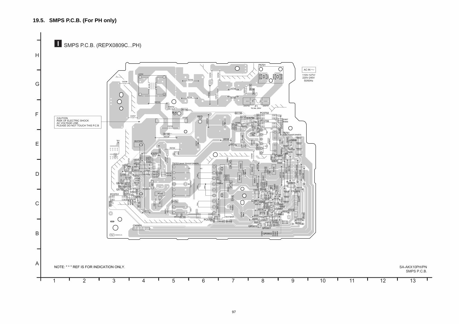
97
19.5. SMPS P.C.B. (For PH only)
17 8 9
E
F
G
H
10 1 12 13
I SMPS P.C.B. (REPX0809C...PH)
SA-AKX10PH/PNSMPS P.C.B.
C57
90
C58
10
C5812
C58
18
C58
31
C58
32
C58
96
C5897
C5898
D5730 PC5702
PC5799
Q5898
R5704
R57
06
R57
86
R5795
R5797
R57
98
R5840
R58
41
R58
02R
5803
R5805
R5806
07 R5809
HEATSINK
R58
14
R58
32
R58
34
R5890
R58
92
R58
93R
5894
R5895
R5705
R5896
R58
91R
5804
C57
96
TP1
R5817
QR5810
R58
00
R5801
R58
60
R58
61
R58
62R
5863
R58
64
R58
97
C5794
C58
19C
5822
C58
69C
5870
D5795
Q5860
Q5861
Q5862
QR5801
QR5802
R58
20
W57
44
D58
04
C57
95
C5800
C58
26
R58
35
R58
33
C58
43
C58
44
R57
09
R57
08
C5798
C58
05
C58
08
C5817
C5899
CN5802
D5701
D57
93D
5798
D58
01D
5802
D58
03
D58
96
IC5799
IC5801
IC5899
R5726
T5751
W5714
W5706
W57
13
W5707
W57
16
W5712
W57
15
W5705
W5717
W5704C
5711
W5718
HEATSINK
W5724
W57
09
W57
03
W5708
W57
25
W5701
W5734
W5730
1
W5702
C57
05
C57
12
C57
01C
5704
DZ
5701
P5701
ZA5701ZA5702
W57
39
W57
38
W57
41
W57
42
C5703
TH5702
K5706
K5705
W57
36
C5706
C5707
F1T6.3AL 250V
K5744
W5743
R5822
R5821(SUB TRANSFORMER)
R5824
R5823
R5826
R5825
R5828
R5827
C57
08
K5743
Q5803
W57
26W
5740
W5728
W57
45
L5703
W5747
W5746
TL7*BLK
TL8*RED
C58
13
W57
48W57
49
CAUTIONRISK OF ELECTRIC SHOCKAC VOLTAGE LINE.PLEASE DO NOT TOUCH THIS P.C.B
K5715
R58
36
R58
37
BCE
BC
E
BC
E
BC
E
BC
E
BC
E
BC
E
BC
E
132
1
3
2
110V-127V/ 220V-240V
50/60Hz
AC IN
PRI SEC
1
2
3
4
5
6
7
8
9
11
10
+1-4 ~3 ~2 1 4
58
10
7
8
9
6
5
4
3
2
1
2
1 4
3
4
32
1
4
3 2
1
1 2 3 4 5 6
A
B
C
D
NOTE: " * " REF IS FOR INDICATION ONLY.
0688CA0688CAPbF
C5720
C57
21
C5722
C5723C5730
D57
21
D5722D5723
D57
24
D5727
D57
32
R5733
(MAIN TRANSFORMER)
R57
02
R5703
R5720
R5721
R57
22
R5732
R58R58
08
PC5701
R58
10
Q5721
R57
24R57
23R
5729
C57
28
Q5722
D57
28
K3
C5726
R57
28
C5820
C58
21
TH5860
D5725 R5730
L5704
PC5720
C57
13
D57
02D5729
D57
31
IC5701
Q5720
W5720
W5723
W5721
W5719
W5722
W57
10
W57
3
W57
35
W5711
T5701
D5726
C5724C
5737
CN5801
K5714
C57
25
BCE
BC
E
BC
E
PRI SEC7
65
43
2
1
1 18
4
2
8
9 10
7
6
5
11
12
13
14
15
16
17
16 5 4 3 2
4
32
1
4
3 2
1

98
19.6. SMPS P.C.B. (For PN only)
17 8 9
E
F
G
H
10 1 12 13
I SMPS P.C.B. (REPX0809A...PN)
SA-AKX10PH/PNSMPS P.C.B.
C58
10
C5812
C58
18
C58
31
C58
32
C58
96
C5897
C5898
D5730 PC5702
PC5799
Q5898
R5704
R57
06
R5795
R5797
R57
98
R5840
R58
41
R58
02R
5803
R5805
R5806
R5809
EATSINK
R58
14
R58
32
R58
34
R5890
R58
92
R58
93R
5894
R5895
R5705
R5896
R58
91R
5804
C57
96
TP1
R5817
QR5810
R58
00
R5801
R58
60
R58
61
R58
62R
5863
R58
64
R58
97
C5794
C58
19C
5822
C58
69C
5870
D5795
Q5860
Q5861
Q5862
QR5801
QR5802
R58
20
W57
44
D58
04
C57
95
C5800
C58
26
C58
43
C58
44
R57
09
R57
08
C5798
C58
05
C58
08
C5817
C5899
CN5802
D5701
D57
98
D58
01D
5802
D58
03
D58
96
IC5799
IC5801
IC5899
R5726
T5751
W5714
W5706
W57
13
W5707
W57
16
W5712
W57
15
W5705
W5717
W5704
W5718
HEATSINK
W5724
W57
09
W57
03
W5708
W57
25
W5701
W5734
W5730
1
W5702C
5705
C57
12R5727
C57
01C
5704
DZ
5701
P5701
ZA5701ZA5702
W57
39
W57
38
W57
41
W57
42
C5703
TH5702
K5706
K5705
W57
36
F18A 125V
K57
11
K5744
W5743
R5822
R5821(SUB TRANSFORMER)
R5824
R5823
R5826
R5825
R5828
R5827
C57
08
K5743
Q5803
W57
26W
5740
W5728
W57
45
L5703
W5747
W5746
C58
13
W57
48W57
49
CAUTIONRISK OF ELECTRIC SHOCKAC VOLTAGE LINE.PLEASE DO NOT TOUCH THIS P.C.B
K5715
BCE
BC
E
BC
E
BC
E
BC
E
BC
E
BC
E
BC
E
132
1
3
2
120V 60Hz
AC IN
PRI SEC
1
2
3
4
5
6
7
8
9
11
10
+1-4 ~3 ~2 1 4
58
10
7
8
9
6
5
4
3
2
1
2
1 4
3
4
32
1
4
3 2
1
1 2 3 4 5 6
A
B
C
D
NOTE: " * " REF IS FOR INDICATION ONLY.
0688AA0688AAPbF
C5720
C57
21
C5722
C5723
C57
25
C5730
D57
21
D5722D5723
D57
24
D5727
D57
32
R5733
(MAIN TRANSFORMER)
R57
02
R5703
R5720
R5721
R57
22
R5732
R5807R58
08
H
PC5701
R58
10
Q5721
R57
24R57
23R
5729
C57
28
Q5722
D57
28
K1
C5726
R57
28
C5820
C58
21
TH5860
D5725 R5730
L5704
PC5720
C57
13
D57
02D5729
D57
31IC5701
Q5720
W5720
W5723
W5721
W5719
W5722
W57
10
W57
3
W57
35
W5711
T5701
D5726
C5724
C57
27
CN5801
K5714
BCE
BC
E
BC
E
PRI SEC7
65
43
2
1
1 18
4
2
8
9 10
7
6
5
11
12
13
14
15
16
17
16 5 4 3 2
4
32
1
4
3 2
1

20 Terminal Function of ICs20.1. IC2801 (RFKWMAKX10PN): IC
MICRO-PROCESSOR
20.2. IC6901(C0HBB0000057): IC FLDriver
Pin No.
Terminal Name I/O Function
1 NC - No Connection2 NC - No Connection3 Mute_F O DAMP MUTE_F4 F_HOP O FHOP for DAMP5 DCDET_DAMP I DC detect input 1 (D.Amp fail-
ure)6 MODE_DA O For digital amp mute7 MUTE A O Audio Mute8 BYTE - External Data Bus width select
input. (GND)9 CNVSS EFP_CNVSS - Flash Mode Terminal
10 XCIN - 32.768kHz sub clock11 XCOUT - 32.768kHz sub clock12 /RESET - /Reset input (Active L)13 XOUT - 10MHz main clock14 VSS - GND (0V)15 XIN - 10MHz main clock16 VCC - Power Supply (+3.3V)17 /NMI - Connected to vcc (3.3V)18 RMT I Remote control Input19 TUN_INT I Tuner Interupt20 SYNC I AC failure detect input21 NC - No Connection22 NC - No Connection23 NC - No Connection24 TUN_RST O Tuner Reset25 TUN_CLK O Tuner CLK26 TUN_DATA I/O Tuner Data27 NC - No Connection28 NC - No Connection29 USB_SCL (RXD)/
WR_ENDI/O USB I2C clock line (Flash Rx for
on board writer)30 USB_SDA (TXD)/ERR I/O USB I2C data line (Flash Tx for
on board writer)31 RXD O RX for Debug32 TXD O TX for Debug33 USB_RST(CLK) O USB reset pin. (Flash Clock for
on board writer)34 BUSY I (Flash Busy for On board writer)35 ASP_DAT I/O ASP DATA36 ASP_CLK I/O ASP_CLK37 NC - No Connection38 NC - No Connection39 NC - No Connection40 NC - No Connection41 NC - No Connection42 NC - No Connection43 NC - No Connection44 NC - No Connection45 NC - No Connection46 NC - No Connection47 NC - No Connection48 NC - No Connection49 SMPS_BP O SMPS_Beat Proof50 NC - No Connection51 DCDET_PWR I DC detect input (Power supply
failure)52 PCONT/EFP/CE O Main transformer control output
53 EE_CS/EFP/EPM O EEPROM chip select (Flash EPM for on board writer)
54 EE_CLK O EEPROM clock55 EE_DAT I/O EEPROM data56 MCLK I/O CD command CLK output57 MDATA_OUT I/O CD command data output58 MLD I/O CD command load output59 STATUS I CD servo LSI status input60 CD RST O CD reset Output61 /RESET_SW(INNER_SW) I CD limit SW Input for the most
inner point(activeLow) (s_ImecINNER)
62 VCC - Power supply (+3.3V)63 CD_LOAD_(H)(TRV_SW) O CD LOAD (H)
(s_OmecTRAY_CW_H)64 VSS - Ground (0V)65 CD_LOAD_(L)(TRV_CCW
)O CD LOAD
(L)(s_OmecTRAY_CCW_H)66 CD OPEN SW I CD OPEN SW
(s_ImecUNLOAD)67 NC - No Connection68 HEADPHONE_SW I Headphone SW69 NC - No Connection70 NC - No Connection71 NC - No Connection72 NC - No Connection73 NC - No Connection74 NC - No Connection75 BLKCK I CD block control Input76 NC - No Connection77 NC - No Connection78 VERR O verify error for USB version up
using CD79 USB_REQ WR_START I Write start flag for USB version
up.80 TERR I Time Out Error for USB81 MMOD0 I Micon mode switching for USB
version up82 FL_CLK O Serial Clock to FL driver83 FL_DOUT O Serial Data to FL driver84 FL_CS O FL driver CS85 CLIP_ATT O Clip Attenuation86 CLIP_SENSOR I CLIP SENSOR87 NC - No Connection88 ROTARY_JOG I Rotary Jog89 REG I Region Setting90 VOL_JOG I Volume Jog91 CS I Chip Select pin92 NC - No Connection93 KEY 2 I Key 2 Input94 KEY 1 I Key 1 input95 BASS_JOG1 I Bass Jog 196 AVSS - Analog power supply input
(Connect to GND)97 BASS_JOG2 I Bass Jog 298 VREF - Reference for AD (3.3V)99 AVCC - Analog power supply input
100 DEMO_SEL I (H= default demo ON, L=default demo OFF)
Pin No.
Terminal Name I/O Function
1 P0 - No Connection
Pin No.
Terminal Name I/O Function
99

2 P1 - No Connection3 P2 - No Connection4 P3 - No Connection5 OSC I Oscillator Input6 NC - No Connection7 DIN I Data Input8 CLK I Clock Input9 STB I Serial Interface Strobe10 K1 - Key Data Input 1 (No Connec-
tion)11 K2 - Key Data Input 2 (No Connec-
tion)12 VSS - GND13 VDD - Power Supply (+5V)14 S1 O Segment Output 1815 S2 O Segment Output 1716 S3 O Segment Output 1617 S4 O Segment Output 1518 S5 O Segment Output 1419 S6 O Segment Output 1320 S7 O Segment Output 1221 S8 O Segment Output 1122 S9 O Segment Output 1023 S10 O Segment Output 924 S11 O Segment Output 825 S12 O Segment Output 726 S13 O Segment Output 627 S14 O Segment Output 528 S15 O Segment Output 429 S16 O Segment Output 330 VEE - Voltage Supply31 G12 O Segment Output 232 G11 O Segment Output 133 G10 O Grid Segment Output 134 G9 O Grid Segment Output 235 G8 O Grid Segment Output 336 G7 O Grid Segment Output 437 G6 O Grid Segment Output538 G5 O Grid Segment Output 639 G4 O Grid Segment Output740 G3 O Grid Segment Output 841 G2 O Grid Segment Output 942 G1 O Grid Segment Output 1043 VDD - Voltage Supply (+5V)44 VSS - GND
Pin No.
Terminal Name I/O Function
100

101
21 Exploded View and Replacement Parts List21.1. Exploded View and Mechanical replacement Part List
21.1.1. Cabinet Parts Location
(USB P.C.B.)
(REMOTE SENSOR P.C.B.)
(PANEL P.C.B.)
(CD OPEN BUTTON P.C.B.)
Z6301
VR6002VR6001
T6101
P903
P901
*ZJ6001B
*ZJ6001A
FL6001
CN6301
CN6002
CN6001
37
36
35
34
33
32
29
25
18
18
18
17
17
16
1616
16
16
16
16
16
16
16
16
16
16
11-1
11-1
11
9
5
3
a
a
b
b
c
c
d
e
7 8 9
F
G
H
10 11 12 13
SA-AKX10PH/PN-K
CABINET DRAWINGS
40
40
38
31
18
18
17
17
17
17
15
14
12
1 2 3 4 5 6
A
B
C
D
E
NOTE: " * " PART IS NOT SUPPLIED / REF IS FOR INDICATION ONLY.

102
(CD MECHANISM
^(VOLTAGE
SELECTOR
P.C.B.)
(SMPS P.C.B.)
(TUNER P.C.B.)
(MAIN P.C.B.)
(D-AMP P.C.B.)
*ZJ5901
*ZJ2701
*TL8
*TL7
*TL6
*TL5
T5751
T5701
^S5701
P5701
JK5901
JK2801
JK52
JK51
F1E2701
CN5902
CN5802
CN5801
CN2711
CN2709
CN2707
CN2706
CN2705
CN2704
CN51
*SMALL
HEATSINK
UNIT
*HEATSINK
UNIT B
*HEATSINK
UNIT A*D-AMP
HEATSINK
UNIT
43
42
41
39
30
3030
303030
28
27
26
23
22
21
20
20
20
20
20
20
20
20
20
20
19
19
18
18
18
18
^18
18
18
18
13
10
8
^7
^6
2
1d
e
f
f
g
h
h
i
i
j
j
k
k
l
l
m
m
7 8 9
E
F
G
H
10 11 12 13
SA-AKX10PH/PN-K
CABINET DRAWINGS
UNIT (DLS6C))
(CD SERVO P.C.B.)
S7202
S7201
CN7002
CN7001
407
407
407
401
43
26
24
21
20
4
g
n
n
1 2 3 4 5 6
A
B
C
D
" ^ " PART IS FOR PH ONLY.NOTE: " * " PART IS NOT SUPPLIED / REF IS FOR INDICATION ONLY.

103
21.1.2. Packaging
SB-AKX10PN
SA-AKX10PH/PN
ACCESSORIES BAG
AC PLUG ADAPTOR
(FOR PH ONLY)
A6
A5 FM INDOOR ANTENNA
A4 AM LOOP ANTENNA
A3 OI BOOK
AC CORD (FOR PN ONLY)
AC CORD (FOR PH ONLY)
A2
A2
R/C BATTERY COVERA1-1A1 REMOTE CONTROL
P3
*P2
*P2
*P2
SC-AKX10PH/PN-K
PACKAGING DRAWINGS
7 8 9
E
F
G
H
10 11 12 13
FRONT
P1
POLYFOAM (TOP FRONT)POLYFOAM (TOP REAR)POLYFOAM (BOTTOM)
*P2
1 2 3 4 5 6
A
B
C
D

104

21.1.3. Mechanical Replacement Part List
Safety Ref. No.
Part No. Part Name & Description
Qty Remarks
CABINET ANDCHASSIS
1 REEX1001 9P FFC (MAIN-TUNER)
1
2 REEX1147 12P FFC (MAIN-DAMP)
1
3 REEX1157 17P FFC (MAIN-PANEL)
1
4 REEX1161 22P FFC (MAIN-CDMECHA)
1
5 REEX1170 22P FFC (USB-MAIN)
1
6 REXX1030 1P RED WIRE(VOLTAGE-SMPS)
1 PH
7 REXX1031 1P BLACK WIRE(VOLTAGE-SMPS)
1 PH
8 REXX1040 6P CABLE WIRE(DAMP-SMPS)
1
9 REXX1076 2P CABLE WIRE(PANEL-CD OPENBUTTON)
1
10 REXX1089 11P CABLE WIRE(SMPS-MAIN)
1
11 RFKGAKX10PHK FRONT PANELASS'Y
1
11-1 RKAX0042-K LEG CUSHION 2
12 RYPX0321H-S D.BASS BUTTONUNIT
1
13 RGRX1002A-A2 REAR PANEL 1 PN
13 RGRX1002B-A2 REAR PANEL 1 PH
14 RGWX0112-S1 VOLUME KNOB 1
15 RGWX0113-S SKIP KNOB 1
16 RHD26046-L SCREW 13
17 RHD30007-K2J SCREW 6
18 RHD30119-S SCREW 13 PH
18 RHD30119-S SCREW 12 PN
19 RHDX031008 SCREW 2
20 RHDX30005-1 SCREW 11
21 RMAX0333-2 CHASSIS SUPPORT 2
22 RMAX1002 D-AMP BRACKET 1
23 RMKX1005 BOTTOM CHASSIS 1
24 RMKX1006 INNER CHASSIS 1
25 RMNV0079-1 FL HOLDER 1
26 RMQX0382-2 MECHA HOLDER 2
27 RMQX1041-Q SUPPORT SHEET 1
28 RMR0502A-W PCB SUPPORT 1
29 RSCV0087B-1 USB CASING TOP 1
30 XTB3+10JFJ SCREW 6
31 RGKX1030-K CD LID 1
32 RGUX1007-K POWER BUTTON 1
33 RGUX1009-K CD OPEN BUTTON 1
34 RGUX1010-S MAIN CONTROLBUTTON L
1
35 RGUX1011-S MAIN CONTROLBUTTON R
1
36 RGUX1016-K MANUAL EQ BUTTON 1
37 RKMX1003-K TOP CABINET 1
38 RMBX1002 CD LID OPENSPRING
1
39 RMCX0035 HEATSINK CLIP A 1
40 RMGX0033 CUSHION RUBBER 2
41 RMNX1025 WIRE HOLDER 1
42 RMQ1702 PCB SUPPORT 1
43 RKAX0042-K LEG CUSHION 2
TRAVERSE DECK
401 RAEX0190Z-V TRAVERSE UNIT 1
407 XTN2+6GFJ SCREW 3
Safety Ref. No.
Part No. Part Name & Description
Qty Remarks
105

PACKING MATERI-ALS
P1 RPGX3065 PACKING CASE 1 PN
P1 RPGX3066 PACKING CASE 1 PH
P2 RPNX1019 POLYFOAM 1
P3 RPFX0198 MIRAMAT SHEET 1
ACCESSORIES
A1 N2QAYB000500 REMOTE CONTROL 1
A1-1 RKK-PT470EBK R/C BATTERYCOVER
1
A2 K2CB2CB00021 AC CORD 1 PN
A2 K2CQ2CA00007 AC CORD 1 PH
A3 RQTX1084-M O/I BOOK (En,Sp) 1
A3 RQTX1085-M O/I BOOK (Sp) 1 PH
A4 N1DYYYY00010 AM LOOP ANTENNA 1
A5 RSAX0002 FM INDOORANTENNA
1
A6 K2DAYYY00002 AC PLUG ADAPTER 1 PH
Safety Ref. No.
Part No. Part Name & Description
Qty Remarks
106

21.2. Electrical Replacement Part List
Safety Ref. No.
Part No. Part Name & Description
Qty Remarks
PRINTED CIRCUITBOARDS
PCB1 REP4557A TUNER P.C.B. 1 (RTL)
PCB2 REPX0636A CD SERVO P.C.B. 1 (RTL)
PCB3 REPX0809A SMPS P.C.B. 1 (RTL)PN
PCB3 REPX0809C SMPS P.C.B. 1 (RTL)PH
PCB4 REPX0814AA MAIN P.C.B. 1 (RTL)PN
PCB4 REPX0814BA MAIN P.C.B. 1 (RTL)PH
PCB5 REPX0814AB PANEL P.C.B. 1 (RTL)PN
PCB5 REPX0814BB PANEL P.C.B. 1 (RTL)PH
PCB6 REPX0814AB CD OPEN BUTTONP.C.B.
1 (RTL)PN
PCB6 REPX0814BB CD OPEN BUTTONP.C.B.
1 (RTL)PH
PCB7 REPX0814AB REMOTE SENSORP.C.B.
1 (RTL)PN
PCB7 REPX0814BB REMOTE SENSORP.C.B.
1 (RTL)PH
PCB8 REPX0814AC USB P.C.B. 1 (RTL)PN
PCB8 REPX0814BC USB P.C.B. 1 (RTL)PH
PCB9 REPX0814AF D-AMP P.C.B. 1 (RTL)PN
PCB9 REPX0814BF D-AMP P.C.B. 1 (RTL)PH
PCB10 REPX0809C VOLTAGE SELEC-TOR P.C.B.
1 (RTL)PH
INTEGRATED CIR-CUITS
IC52 VUEALLPT031 IC 1 [SPG]
IC900 MNZSFB5KJM2 IC 1
IC2101 C1BB00001151 IC 1
IC2201 C0AABB000125 IC 1
IC2701 C0CAAKG00046 IC 1
IC2702 C0DAAYG00001 IC 1
IC2801 RFKWMAKX10PN IC 1
IC2802 C3EBFY000006 IC 1
IC5701 C5HACYY00004 IC 1 PN
IC5701 C5HACYY00005 IC 1 PH
IC5799 MIP2F20MSSCF IC 1
IC5801 C0DABFC00002 IC 1
IC5899 C0DAEMZ00001 IC 1
IC5900 C1BA00000497 IC 1
IC6001 C0HBB0000061 IC 1
IC7001 MN6627954AMA IC 1
IC7002 BA5948FPE2 IC 1
TRANSISTORS
Q2220 B1ABCF000176 TRANSISTOR 1
Q2221 B1ABCF000176 TRANSISTOR 1
Q2222 B1ABCF000176 TRANSISTOR 1
Q2223 B1ABCF000176 TRANSISTOR 1
Q2301 B1ABCF000176 TRANSISTOR 1
Q2302 B1ABCF000176 TRANSISTOR 1
Q2701 B1BACG000023 TRANSISTOR 1
Q2702 B1AAJC000019 TRANSISTOR 1
Q2705 B1ADCE000012 TRANSISTOR 1
Q2790 B1ABCF000176 TRANSISTOR 1
Q2803 B1ACKD000006 TRANSISTOR 1
Q5720 B1BABG000007 TRANSISTOR 1
Q5721 B1ADCF000001 TRANSISTOR 1
Q5722 B1ABCF000176 TRANSISTOR 1
Q5803 B1BABG000007 TRANSISTOR 1
Q5860 B1ADCF000001 TRANSISTOR 1
Q5861 B1ABCF000176 TRANSISTOR 1
Q5862 B1GBCFJJ0051 TRANSISTOR 1
Q5898 B1ABCF000176 TRANSISTOR 1
Safety Ref. No.
Part No. Part Name & Description
Qty Remarks
107

Q5901 B1ABGC000005 TRANSISTOR 1
Q5902 B1ADCE000012 TRANSISTOR 1
Q5903 B1ABCF000176 TRANSISTOR 1
Q5905 B1ABCF000176 TRANSISTOR 1
Q5906 B1ABCF000176 TRANSISTOR 1
Q5907 B1ABCF000176 TRANSISTOR 1
Q6101 B1BABK000001 TRANSISTOR 1
Q7601 B1ADCF000001 TRANSISTOR 1
QR2701 B1GBCFJJ0051 TRANSISTOR 1
QR2702 B1GBCFJJ0051 TRANSISTOR 1
QR2704 B1GBCFJJ0051 TRANSISTOR 1
QR2801 B1GBCFLL0037 TRANSISTOR 1
QR2802 B1GBCFLL0037 TRANSISTOR 1
QR2831 B1GDCFGG0026 TRANSISTOR 1
QR2832 B1GDCFGG0026 TRANSISTOR 1
QR5801 B1GBCFJN0038 TRANSISTOR 1
QR5802 B1GDCFGA0018 TRANSISTOR 1
QR5810 B1GBCFLL0037 TRANSISTOR 1
QR5900 B1GBCFJJ0051 TRANSISTOR 1
QR5901 B1GDCFJJ0047 TRANSISTOR 1
DIODES
D2120 B0EAKM000117 DIODE 1
D2602 B0ACCK000012 DIODE 1
D2603 B0ACCK000012 DIODE 1
D2604 B0ACCK000012 DIODE 1
D2605 B0ACCK000012 DIODE 1
D2704 B0BC8R2A0266 DIODE 1
D2706 B0EAKM000117 DIODE 1
D2707 B0EAKM000117 DIODE 1
D2708 B0EAKM000117 DIODE 1
D2709 B0ACCK000012 DIODE 1
D2710 B0ACCK000012 DIODE 1
D2711 B0ADCJ000020 DIODE 1
D2790 B0ACCK000012 DIODE 1
D2801 B0ACCK000012 DIODE 1
D2802 B0ACCK000012 DIODE 1
D2803 B0ACCK000012 DIODE 1
D2804 B0BC5R1A0266 DIODE 1
D5701 B0FBAR000043 DIODE 1
D5702 B0ZAZ0000052 DIODE 1
D5721 B0BC010A0007 DIODE 1 PH
D5721 B0BC018A0267 DIODE 1 PN
D5722 B0BC019A0007 DIODE 1
D5723 B0ACCK000012 DIODE 1
D5724 B0ACCK000012 DIODE 1
D5725 B0BC6R100010 DIODE 1
D5726 B0EAKM000117 DIODE 1
D5727 B0ACCK000012 DIODE 1
D5728 B0ACCK000012 DIODE 1
D5729 B0EAMM000057 DIODE 1
D5730 MA2YF8000L DIODE 1
D5731 B0EAMM000057 DIODE 1
D5732 B0BC035A0007 DIODE 1
D5793 B0HAMP000094 DIODE 1 PH
D5795 B0BC9R000008 DIODE 1
D5798 B0EAMM000057 DIODE 1
D5801 B0ABSM000008 DIODE 1
D5802 B0ABSM000008 DIODE 1
D5803 B0HFRJ000012 DIODE 1
D5804 B0ACCK000012 DIODE 1
D5896 B0EAMM000057 DIODE 1
D5903 B0HCSP000001 DIODE 1
D5904 B0HCSP000001 DIODE 1
D5905 B0HCSP000001 DIODE 1
D5906 B0HCSP000001 DIODE 1
D6001 B0BC2R4A0263 DIODE 1
D6101 B0BC024A0269 DIODE 1
D6102 B0JAME000114 DIODE 1
D6103 B0EAMM000057 DIODE 1
D6104 B0EAMM000057 DIODE 1
D6105 B0BC036A0264 DIODE 1
D7650 MAZ8056GML DIODE 1
Safety Ref. No.
Part No. Part Name & Description
Qty Remarks
DZ2701 B0JCPD000025 DIODE 1
DZ5701 ERZV10V511CS ZNR 1
VARISTORS
VA51 EZAEG2A50AX ESD SUPRESSOR 1
VARIABLE RESIS-TORS
VR6001 EVEKE2F3524B VOLUME JOG 1
VR6002 K9AA012Y0004 VR ENCODER 1
SWITCHES
S5701 K0ABCA000007 SW VOLTAGESELECTOR
1 PH
S6001 EVQ21405RJ SW POWER 1
S6002 EVQ21405RJ SW STOP/DEMO 1
S6003 EVQ21405RJ SW AUX 1
S6004 EVQ21405RJ SW USB 1
S6005 EVQ21405RJ SW D. BASS 1
S6006 EVQ21405RJ SW MANUAL_EQ 1
S6007 EVQ21405RJ SW EQ+/FWD 1
S6008 EVQ21405RJ SW EQ-/REW 1
S6009 EVQ21405RJ SW ALBUM+ 1
S6010 EVQ21405RJ SW ALBUM- 1
S6011 EVQ21405RJ SW CD 1
S6012 EVQ21405RJ SW FM/AM 1
S6201 EVQ21405RJ SW OPEN/CLOSE 1
S7201 RSH1A045-1A SW RESET 1
S7202 RSH1A045-1A SW CD OPEN 1
CONNECTORS
CN51 K1MN09AA0003 9P CONNECTOR 1
CN2704 K1MN22AA0004 22P CONNECTOR 1
CN2705 K1MN09AA0003 9P CONNECTOR 1
CN2706 K1MN22AA0004 22P CONNECTOR 1
CN2707 K1MN08B00013 8P CONNECTOR 1
CN2709 K1MY17AA0124 17P CONNECTOR 1
CN2711 K1MN12AA0003 12P CONNECTOR 1
CN5801 K1KA06AA0180 6P CONNECTOR 1
CN5802 K1KA11AA0194 11P CONNECTOR 1
CN5902 K1MN12AA0003 12P CONNECTOR 1
CN6001 K1KA04AA0031 4P CONNECTOR 1
CN6002 K1MY17AA0124 17P CONNECTOR 1
CN6301 K1KB04A00046 4P CONNECTOR 1
CN7001 K1MN16B00154 16P CONNECTOR 1
CN7002 K1MN22BA0005 22P CONNECTOR 1
P901 K1MN22BA0005 22P CONNECTOR 1
P903 K1FY104B0011 USB CONNECTOR 1
COILS AND INDUC-TORS
L51 G1CR18JA0020 INDUCTOR 1
L52 G2A380Y00001 ANTENNA COIL 1
L900 G1C100K00019 INDUCTOR 1
L2140 G0C470JA0055 INDUCTOR 1
L2702 G0A101ZA0028 CHOKE COIL 1
L2801 G0A220GA0002 CHOKE COIL 1
L5703 G0B612H00002 LINE FILTER 1
L5704 J0JBC0000019 INDUCTOR 1
L5901 J0JKB0000020 INDUCTOR 1
L5902 J0JKB0000020 INDUCTOR 1
L5903 G0A150L00003 CHOKE COIL 1
L5904 G0B9R5K00005 LINE FILTER 1
L5905 G0B9R5K00005 LINE FILTER 1
L6001 J0JBC0000019 INDUCTOR 1
L6101 G0A220GA0002 CHOKE COIL 1
LB51 J0JBC0000032 INDUCTOR 1
TRANSFORMERS
T5701 ETS39AG4M6AD MAIN TRANSFORMER 1 PH
T5701 ETS39AG4NGAD MAIN TRANSFORMER 1 PN
T5751 ETS19AB2E6AG SUB TRANSFORMER 1
Safety Ref. No.
Part No. Part Name & Description
Qty Remarks
108

T6101 G4DYA0000214 SWITCHING TRANS-FORMER
1
COMPONENT COMBI-NATION
Z6301 B3RAB0000084 REMOTE SENSOR 1
PHOTO COUPLERS
PC5701 B3PBA0000402 PHOTO COUPLER 1
PC5702 B3PBA0000402 PHOTO COUPLER 1
PC5720 B3PBA0000402 PHOTO COUPLER 1
PC5799 B3PBA0000402 PHOTO COUPLER 1
OSCILLATORS
X51 H0A327200097 CRYSTAL OSCILLA-TOR
1
X900 H0A120500009 CRYSTAL OSCILLA-TOR
1
X2801 H0A327200097 CRYSTAL OSCILLA-TOR
1
X2802 H2B100500004 CRYSTAL OSCILLA-TOR
1
X7201 H0H169500013 CRYSTAL OSCILLA-TOR
1
FL DISPLAY
FL6001 A2BB00000171 LCD DISPLAY 1
FUSES
F1 K5D632BK0007 FUSE 1 PH
F1 K5D802APA008 FUSE 1 PN
FUSE HOLDERS
ZA5701 K3GE1ZZ00001 FUSE HOLDER 1
ZA5702 K3GE1ZZ00001 FUSE HOLDER 1
THERMISTORS
TH5702 D4CAA2R20001 THERMISTOR 1
TH5860 D4CC11040013 THERMISTOR 1
TH5900 D4CC11040013 THERMISTOR 1
JACKS
JK51 K4ZZ02000103 JK FM ANT 1
JK52 K4AC02B00042 JK AM ANT 1
JK2801 K2HA204B0153 JK AUX 1
JK5901 K4AL04B00001 JK SPEAKER 1
P5701 K2AA2B000011 AC INLET 1 PH
P5701 K2AB2B000007 AC INLET 1 PN
EARTH TERMINALS
E2701 K4CZ01000027 TERMINAL 1
CHIP JUMPERS
K1 D0GBR00JA008 0 1/16W 1 PN
K3 D0GBR00JA008 0 1/16W 1 PH
K2706 D0GBR00JA008 0 1/16W 1
LB852 D0GBR00JA008 0 1/16W 1
LB951 D0GBR00JA008 0 1/16W 1
LB952 D0GBR00JA008 0 1/16W 1
LB7262 D0GBR00JA008 0 1/16W 1
LB7263 D0GBR00JA008 0 1/16W 1
LB7264 D0GBR00JA008 0 1/16W 1
W21 D0GDR00JA017 0 1/10W 1
W22 D0GBR00JA008 0 1/16W 1
W23 D0GBR00JA008 0 1/16W 1
W24 D0GBR00JA008 0 1/16W 1
W25 D0GDR00JA017 0 1/10W 1
W26 D0GDR00JA017 0 1/10W 1
W27 D0GDR00JA017 0 1/10W 1
W28 D0GBR00JA008 0 1/16W 1
W29 D0GDR00JA017 0 1/10W 1
W30 D0GDR00JA017 0 1/10W 1
W31 D0GBR00JA008 0 1/16W 1
Safety Ref. No.
Part No. Part Name & Description
Qty Remarks
W2501 D0GDR00JA017 0 1/10W 1
W2502 D0GBR00JA008 0 1/16W 1
W2503 D0GBR00JA008 0 1/16W 1
W2504 D0GDR00JA017 0 1/10W 1
W2505 D0GBR00JA008 0 1/16W 1
W2507 D0GBR00JA008 0 1/16W 1
W2508 D0GBR00JA008 0 1/16W 1
W2509 D0GDR00JA017 0 1/10W 1
W2510 D0GBR00JA008 0 1/16W 1
W2511 D0GBR00JA008 0 1/16W 1
W2512 D0GDR00JA017 0 1/10W 1
W2513 D0GDR00JA017 0 1/10W 1
W2514 D0GDR00JA017 0 1/10W 1
W2515 D0GBR00JA008 0 1/16W 1
W2516 D0GDR00JA017 0 1/10W 1
W5033 D0GBR00JA008 0 1/16W 1
W5039 D0GBR00JA008 0 1/16W 1
W5040 D0GDR00JA017 0 1/10W 1
W5041 D0GBR00JA008 0 1/16W 1
W5042 D0GDR00JA017 0 1/10W 1
W5043 D0GDR00JA017 0 1/10W 1
W5044 D0GDR00JA017 0 1/10W 1
W5045 D0GBR00JA008 0 1/16W 1
W5046 D0GDR00JA017 0 1/10W 1
W5047 D0GBR00JA008 0 1/16W 1
W5744 D0GBR00JA008 0 1/16W 1
W6101 D0GDR00JA017 0 1/10W 1
W7001 D0GBR00JA008 0 1/16W 1
W7002 D0GBR00JA008 0 1/16W 1
W7003 D0GBR00JA008 0 1/16W 1
W7004 D0GBR00JA008 0 1/16W 1
W7005 D0GBR00JA008 0 1/16W 1
W7006 D0GBR00JA008 0 1/16W 1
W7007 D0GBR00JA008 0 1/16W 1
W7008 D0GBR00JA008 0 1/16W 1
W7009 D0GBR00JA008 0 1/16W 1
W7010 D0GBR00JA008 0 1/16W 1
W7011 D0GBR00JA008 0 1/16W 1
W7012 D0GBR00JA008 0 1/16W 1
W7013 D0GBR00JA008 0 1/16W 1
W7014 D0GBR00JA008 0 1/16W 1
W7015 D0GBR00JA008 0 1/16W 1
W7016 D0GBR00JA008 0 1/16W 1
W7017 D0GBR00JA008 0 1/16W 1
W7018 D0GBR00JA008 0 1/16W 1
W7019 D0GBR00JA008 0 1/16W 1
W7020 D0GBR00JA008 0 1/16W 1
W7021 D0GBR00JA008 0 1/16W 1
W7024 D0GBR00JA008 0 1/16W 1
W7025 D0GDR00JA017 0 1/10W 1
W7026 D0GDR00JA017 0 1/10W 1
RESISTORS
R51 D0GB102JA008 1K 1/16W 1
R52 D0GB102JA008 1K 1/16W 1
R53 D0GA472JA023 4.7K 1/16W 1
R54 D0GA472JA023 4.7K 1/16W 1
R55 D0GA221JA023 220 1/16W 1
R56 D0GB221JA007 220 1/10W 1
R57 D0GA102JA023 1K 1/16W 1
R59 D0GB222JA008 2.2K 1/16W 1
R61 D0GB473JA008 47K 1/16W 1
R62 D0GB473JA008 47K 1/16W 1
R64 D0GBR00JA008 0 1/16W 1
R901 D0GB102JA008 1K 1/16W 1
R902 D0GB102JA008 1K 1/16W 1
R903 D0GBR00JA008 0 1/16W 1
R904 D0GBR00JA008 0 1/16W 1
R906 D0GBR00JA008 0 1/16W 1
R907 D0GDR00JA017 0 1/10W 1
R914 D0GBR00JA008 0 1/16W 1
R950 D0GBR00JA008 0 1/16W 1
R952 D0GB240JA008 24 1/16W 1
Safety Ref. No.
Part No. Part Name & Description
Qty Remarks
109
R953 D0GB240JA008 24 1/16W 1
R954 D0GB153JA008 15K 1/16W 1
R955 D0GB153JA008 15K 1/16W 1
R957 D0GB222JA008 2.2K 1/16W 1
R958 D0GB104JA008 100K 1/16W 1
R971 D0GB102JA008 1K 1/16W 1
R972 D0GB102JA008 1K 1/16W 1
R2005 D0GB473JA008 47K 1/16W 1
R2006 D0GB473JA008 47K 1/16W 1
R2009 D0GB332JA008 3.3K 1/16W 1
R2101 D0GB332JA008 3.3K 1/16W 1
R2102 D0GB332JA008 3.3K 1/16W 1
R2105 D0GB682JA008 6.8K 1/16W 1
R2108 D0GB682JA008 6.8K 1/16W 1
R2113 D0GB272JA008 2.7K 1/16W 1
R2114 D0GB272JA008 2.7K 1/16W 1
R2130 D0GBR00JA008 0 1/16W 1
R2201 D0GB102JA008 1K 1/16W 1
R2202 D0GB102JA008 1K 1/16W 1
R2203 D0GBR00JA008 0 1/16W 1
R2204 D0GBR00JA008 0 1/16W 1
R2205 D0GB562JA008 5.6K 1/16W 1
R2206 D0GB562JA008 5.6K 1/16W 1
R2207 D0GB273JA008 27K 1/16W 1
R2208 D0GB273JA008 27K 1/16W 1
R2220 D0GB222JA008 2.2K 1/16W 1
R2221 D0GB472JA008 4.7K 1/16W 1
R2222 D0GB472JA008 4.7K 1/16W 1
R2223 D0GB104JA008 100K 1/16W 1
R2224 D0GB102JA008 1K 1/16W 1
R2225 D0GB272JA008 2.7K 1/16W 1
R2226 D0GB472JA008 4.7K 1/16W 1
R2227 D0GB104JA008 100K 1/16W 1
R2228 D0GB102JA008 1K 1/16W 1
R2229 D0GB272JA008 2.7K 1/16W 1
R2230 D0GB563JA008 56K 1/16W 1
R2231 D0GB563JA008 56K 1/16W 1
R2303 D0GB101JA008 100 1/16W 1
R2304 D0GB101JA008 100 1/16W 1
R2305 D0GB331JA008 330 1/16W 1
R2306 D0GB331JA008 330 1/16W 1
R2307 D0GB222JA008 2.2K 1/16W 1
R2308 D0GB222JA008 2.2K 1/16W 1
R2309 D0GB222JA008 2.2K 1/16W 1
R2310 D0GB222JA008 2.2K 1/16W 1
R2311 D0GB102JA008 1K 1/16W 1
R2312 D0GB102JA008 1K 1/16W 1
R2313 D0GB104JA008 100K 1/16W 1
R2314 D0GB104JA008 100K 1/16W 1
R2601 D0GB475JA008 4.7M 1/16W 1
R2602 D0GB223JA008 22K 1/16W 1
R2604 D0GB223JA008 22K 1/16W 1
R2605 D0GB104JA008 100K 1/16W 1
R2606 D0GB223JA008 22K 1/16W 1
R2608 D0GB104JA008 100K 1/16W 1
R2611 D0GB223JA008 22K 1/16W 1
R2701 D0GB101JA008 100 1/16W 1
R2702 D0GB391JA008 390 1/16W 1
R2704 D0GB102JA008 1K 1/16W 1
R2705 D0GB472JA008 4.7K 1/16W 1
R2706 D0HB152ZA002 1.5K 1/16W 1
R2707 D0HB102ZA002 1K 1/16W 1
R2708 ERJ3RBD272V 2.7K 1/16W 1
R2710 D0GB105JA008 1M 1/16W 1
R2718 D0GB2R2JA008 2.2 1/16W 1
R2719 D0GB2R2JA008 2.2 1/16W 1
R2720 D0GB2R2JA008 2.2 1/16W 1
R2721 D0GB271JA008 270 1/16W 1
R2772 D0GB123JA008 12K 1/16W 1
R2773 D0GB153JA008 15K 1/16W 1
R2774 D0GB223JA008 22K 1/16W 1
R2790 D0GB222JA008 2.2K 1/16W 1
R2791 D0GB222JA008 2.2K 1/16W 1
Safety Ref. No.
Part No. Part Name & Description
Qty Remarks
R2802 D0GB104JA008 100K 1/16W 1
R2805 D0GB103JA008 10K 1/16W 1
R2809 D0GB472JA008 4.7K 1/16W 1
R2810 D0GB223JA008 22K 1/16W 1
R2812 D0GB472JA008 4.7K 1/16W 1
R2815 D0GB332JA008 3.3K 1/16W 1
R2816 D0GB122JA008 1.2K 1/16W 1 PH
R2816 D0GBR00JA008 0 1/16W 1 PN
R2817 D0GB103JA008 10K 1/16W 1
R2821 D0GB102JA008 1K 1/16W 1
R2822 D0GB101JA008 100 1/16W 1
R2824 D0GB101JA008 100 1/16W 1
R2825 D0GB473JA008 47K 1/16W 1
R2826 D0GB473JA008 47K 1/16W 1
R2827 D0GB103JA008 10K 1/16W 1
R2828 D0GB101JA008 100 1/16W 1
R2829 D0GB101JA008 100 1/16W 1
R2830 D0GB101JA008 100 1/16W 1
R2831 D0GB101JA008 100 1/16W 1
R2834 D0GB473JA008 47K 1/16W 1
R2835 D0GB103JA008 10K 1/16W 1
R2836 D0GB102JA008 1K 1/16W 1
R2838 D0GB102JA008 1K 1/16W 1
R2839 D0GB101JA008 100 1/16W 1
R2840 D0GB223JA008 22K 1/16W 1
R2841 D0GB101JA008 100 1/16W 1
R2842 D0GB101JA008 100 1/16W 1
R2843 D0GB101JA008 100 1/16W 1
R2846 D0GB101JA008 100 1/16W 1
R2847 D0GB106JA008 10M 1/16W 1
R2848 D0GBR00JA008 0 1/16W 1
R2849 D0GB102JA008 1K 1/16W 1
R2850 D0GB105JA008 1M 1/16W 1
R2851 D0GB102JA008 1K 1/16W 1
R2852 D0GB101JA008 100 1/16W 1
R2853 D0GB221JA007 220 1/10W 1
R2854 D0GB152JA008 1.5K 1/16W 1
R2855 D0GB152JA008 1.5K 1/16W 1
R2856 D0GB102JA008 1K 1/16W 1
R2857 D0GB101JA008 100 1/16W 1
R2858 D0GB101JA008 100 1/16W 1
R2859 D0GB103JA008 10K 1/16W 1
R2860 D0GB102JA008 1K 1/16W 1
R2862 D0GB101JA008 100 1/16W 1
R2863 D0GB102JA008 1K 1/16W 1
R2864 D0GB101JA008 100 1/16W 1
R2865 D0GB101JA008 100 1/16W 1
R2866 D0GB102JA008 1K 1/16W 1
R2867 D0GB101JA008 100 1/16W 1
R2868 D0GB101JA008 100 1/16W 1
R2869 D0GB101JA008 100 1/16W 1
R2870 D0GB101JA008 100 1/16W 1
R2871 D0GB102JA008 1K 1/16W 1
R2872 D0GB101JA008 100 1/16W 1
R2873 D0GB223JA008 22K 1/16W 1
R2874 D0GB103JA008 10K 1/16W 1
R2875 D0GB473JA008 47K 1/16W 1
R2877 D0GB153JA008 15K 1/16W 1
R2878 D0GB153JA008 15K 1/16W 1
R2879 D0GB103JA008 10K 1/16W 1
R2880 D0GB101JA008 100 1/16W 1
R2881 D0GB101JA008 100 1/16W 1
R2882 D0GB101JA008 100 1/16W 1
R2883 D0GB473JA008 47K 1/16W 1
R2884 D0GB101JA008 100 1/16W 1
R2885 D0GB101JA008 100 1/16W 1
R2886 D0GB101JA008 100 1/16W 1
R2887 D0GB392JA008 3.9K 1/16W 1
R2888 D0GB392JA008 3.9K 1/16W 1
R2889 D0GB472JA008 4.7K 1/16W 1
R2890 D0GB223JA008 22K 1/16W 1
R2891 D0GB102JA008 1K 1/16W 1
R2892 D0GB223JA008 22K 1/16W 1
Safety Ref. No.
Part No. Part Name & Description
Qty Remarks
110

R2893 D0GB474JA008 470K 1/16W 1
R2894 D0GB103JA008 10K 1/16W 1
R5702 D0GZ104JA012 100K 1W 1 PH
R5702 D0GZ333JA012 33K 1W 1 PN
R5703 D0GZ104JA012 100K 1W 1 PH
R5703 D0GZ333JA012 33K 1W 1 PN
R5704 ERJ8GEYJ224V 220K 1/4W 1
R5705 ERJ8GEYJ224V 220K 1/4W 1
R5706 D0GD824JA017 820K 1/8W 1
R5708 ERJ8GEYJ155V 1.5M 1/4W 1
R5709 ERJ8GEYJ155V 1.5M 1/4W 1
R5720 D0GD220JA017 22 1/10W 1
R5721 D0GD103JA017 10K 1/10W 1
R5722 D0GD122JA017 1.2K 1/10W 1
R5723 D0GB102JA008 1K 1/16W 1
R5724 D0GD121JA017 120 1/10W 1
R5726 ERX2SZJR10P 0.1 2W 1 PH
R5726 ERX2SZJR15P 0.15 2W 1 PN
R5727 ERX2SZJR13P 0.13 2W 1 PN
R5728 D0GB104JA008 100K 1/16W 1
R5729 D0GD103JA017 10K 1/10W 1
R5730 D0GB102JA008 1K 1/16W 1
R5732 D0GB101JA008 100 1/16W 1
R5733 D0GB473JA008 47K 1/16W 1
R5786 D0GZ204JA012 100K 1W 1 PH
R5795 D0GD474JA017 470K 1/8W 1
R5797 D0GB153JA008 15K 1/16W 1
R5798 D0GB220JA008 22 1/16W 1
R5800 D0GD153JA017 15K 1/10W 1
R5801 D0GD223JA017 22K 1/10W 1
R5802 D0HB123ZA002 12K 1/16W 1
R5803 D0HB102ZA002 1K 1/16W 1
R5804 D1BD4702A077 47K 1/10W 1
R5805 ERJ3RBD222V 2.2K 1/16W 1
R5806 D0GB153JA008 15K 1/16W 1
R5807 D0GD331JA017 330 1/8W 1
R5808 D0GD222JA017 2.2K 1/10W 1
R5809 D0GD331JA017 330 1/8W 1
R5810 D0GB331JA008 330 1/16W 1
R5814 D0GB822JA008 8.2K 1/16W 1
R5817 D0GB331JA008 330 1/16W 1
R5820 D0GB103JA008 10K 1/16W 1
R5821 ERG2SJ471E 470 2W 1
R5822 ERG2SJ471E 470 2W 1
R5823 ERG2SJ471E 470 2W 1
R5824 ERG2SJ471E 470 2W 1
R5825 ERG2SJ471E 470 2W 1
R5826 ERG2SJ471E 470 2W 1
R5827 ERG2SJ471E 470 2W 1
R5828 ERG2SJ471E 470 2W 1
R5832 D0GZ222JA012 2.2K 1W 1
R5833 D0GZ222JA012 2.2K 1W 1 PH
R5834 D0GZ222JA012 2.2K 1W 1
R5835 D0GZ222JA012 2.2K 1W 1 PH
R5836 D0GZ222JA012 2.2K 1W 1 PH
R5837 D0GZ222JA012 2.2K 1W 1 PH
R5840 D0GB823JA008 82K 1/16W 1
R5841 D0GB124JA008 120K 1/16W 1
R5860 ERJ3GEYF103V 10K 1/10W 1
R5861 ERJ3GEYF472V 4.7K 1/10W 1
R5862 D0GD183JA017 18K 1/8W 1
R5863 D0GD183JA017 18K 1/8W 1
R5864 ERJ3GEYF103V 10K 1/10W 1
R5890 D0GB222JA008 2.2K 1/16W 1
R5891 ERJ3RBD333V 33K 1/16W 1
R5892 D0HB102ZA002 1K 1/16W 1
R5893 ERJ3RBD103V 10K 1/16W 1
R5894 D0GB151JA008 150 1/16W 1
R5895 D0GB153JA008 15K 1/16W 1
R5896 D0GB104JA008 100K 1/16W 1
R5897 D0GB101JA008 100 1/16W 1
R5901 D0GB124JA008 120K 1/16W 1
R5903 D0GB103JA008 10K 1/16W 1
Safety Ref. No.
Part No. Part Name & Description
Qty Remarks
R5904 D0GB103JA008 10K 1/16W 1
R5905 D0GF100JA014 10 1/8W 1
R5906 D0GB184JA008 180K 1/16W 1
R5907 ERJ3RBD273V 27K 1/16W 1
R5908 D0GB103JA008 10K 1/16W 1
R5909 ERJ3RBD333V 33K 1/16W 1
R5910 D0HB152ZA002 1.5K 1/16W 1
R5911 D0GB562JA008 5.6K 1/16W 1
R5913 ERJ3RBD272V 2.7K 1/16W 1
R5914 D0GB562JA008 5.6K 1/16W 1
R5915 D0GB103JA008 10K 1/16W 1
R5917 D0GF100JA014 10 1/8W 1
R5918 ERJ3RBD272V 2.7K 1/16W 1
R5921 D0GF100JA014 10 1/8W 1
R5922 D0GF100JA014 10 1/8W 1
R5923 D0GB682JA008 6.8K 1/16W 1
R5924 D0GB562JA008 5.6K 1/16W 1
R5925 D0GB562JA008 5.6K 1/16W 1
R5926 D0GB101JA008 100 1/16W 1
R5927 D0GB823JA008 82K 1/16W 1
R5928 D0GB823JA008 82K 1/16W 1
R5931 ERJ1TYJ220U 22 1W 1
R5932 ERJ1TYJ220U 22 1W 1
R5933 D0GB562JA008 5.6K 1/16W 1
R5934 D0GB562JA008 5.6K 1/16W 1
R5935 D0GB103JA008 10K 1/16W 1
R6001 D0GB122JA008 1.2K 1/16W 1
R6002 D0GB152JA008 1.5K 1/16W 1
R6003 D0GB222JA008 2.2K 1/16W 1
R6004 D0GB332JA008 3.3K 1/16W 1
R6005 D0GB682JA008 6.8K 1/16W 1
R6006 D0GB122JA008 1.2K 1/16W 1
R6007 D0GB152JA008 1.5K 1/16W 1
R6008 D0GB222JA008 2.2K 1/16W 1
R6009 D0GB332JA008 3.3K 1/16W 1
R6010 D0GB472JA008 4.7K 1/16W 1
R6012 D0GB103JA008 10K 1/16W 1
R6013 D0GB103JA008 10K 1/16W 1
R6014 D0GB221JA007 220 1/10W 1
R6015 D0GB221JA007 220 1/10W 1
R6016 D0GB471JA008 470 1/16W 1
R6017 D0GB823JA008 82K 1/16W 1
R6018 D0GB103JA008 10K 1/16W 1
R6019 D0GB223JA008 22K 1/16W 1
R6020 D0GB123JA008 12K 1/16W 1
R6021 D0GB100JA008 10 1/16W 1
R6022 D0GB123JA008 12K 1/16W 1
R6023 D0GB223JA008 22K 1/16W 1
R6024 D0GB103JA008 10K 1/16W 1
R6025 D0GB223JA008 22K 1/16W 1
R6028 D0GB102JA008 1K 1/16W 1
R6101 D0GB473JA008 47K 1/16W 1
R6102 D0GB470JA008 47 1/16W 1
R6103 D0GBR00JA008 0 1/16W 1
R6105 D0GB682JA008 6.8K 1/16W 1
R6106 D0GD1R0JA017 1.0 1/8W 1
R6108 D0GD1R0JA017 1.0 1/8W 1
R6201 D0GB472JA008 4.7K 1/16W 1
R7111 D0GB103JA008 10K 1/16W 1
R7211 D0GB823JA008 82K 1/16W 1
R7212 D0GB821JA008 820 1/16W 1
R7214 D0GB471JA008 470 1/16W 1
R7217 D0GB102JA008 1K 1/16W 1
R7218 D0GB102JA008 1K 1/16W 1
R7220 D0GB105JA008 1M 1/16W 1
R7221 D0GB101JA008 100 1/16W 1
R7253 D0GB100JA008 10 1/16W 1
R7254 D0GB102JA008 1K 1/16W 1
R7315 D0GB332JA008 3.3K 1/16W 1
R7323 D0GB682JA008 6.8K 1/16W 1
R7325 D0GB331JA008 330 1/16W 1
R7327 D0GB102JA008 1K 1/16W 1
R7328 D0GB103JA008 10K 1/16W 1
Safety Ref. No.
Part No. Part Name & Description
Qty Remarks
111
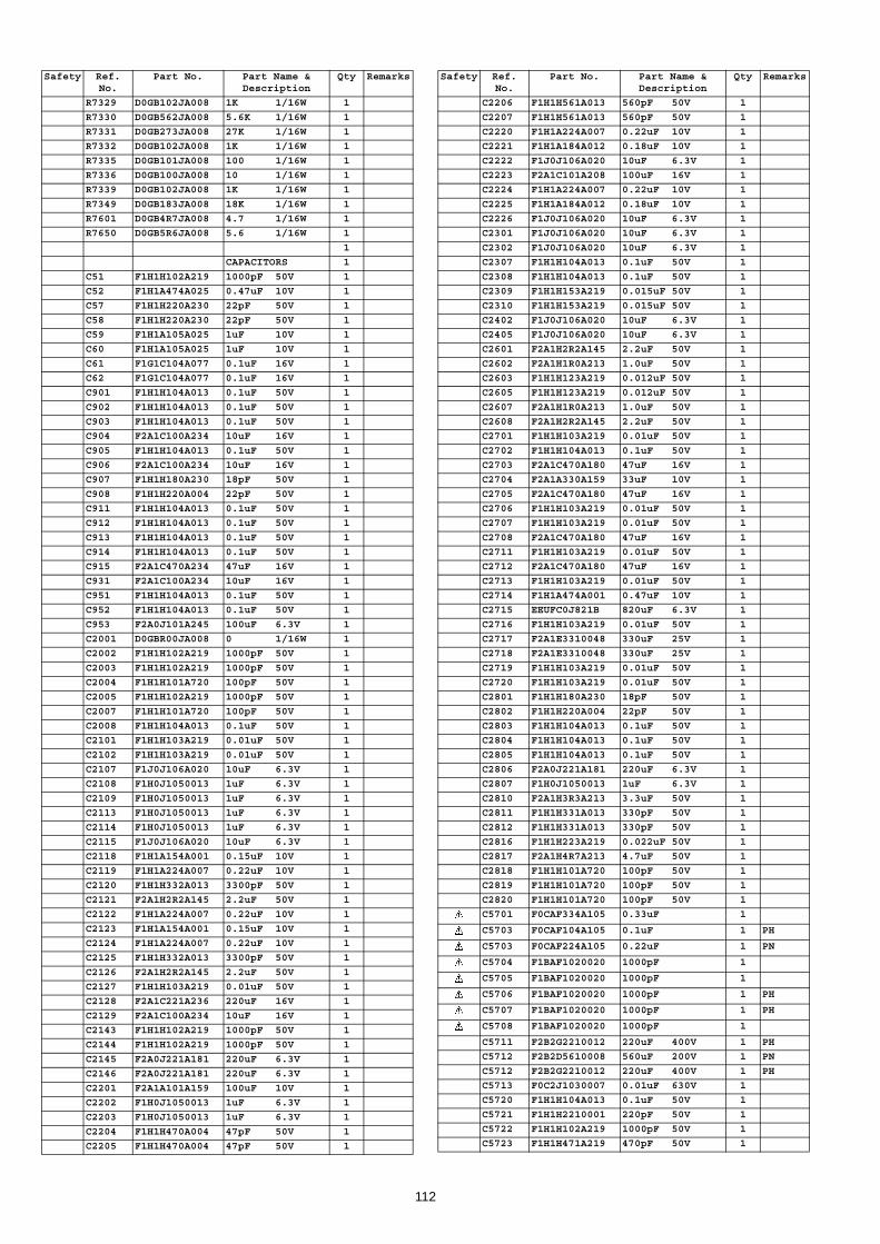
R7329 D0GB102JA008 1K 1/16W 1
R7330 D0GB562JA008 5.6K 1/16W 1
R7331 D0GB273JA008 27K 1/16W 1
R7332 D0GB102JA008 1K 1/16W 1
R7335 D0GB101JA008 100 1/16W 1
R7336 D0GB100JA008 10 1/16W 1
R7339 D0GB102JA008 1K 1/16W 1
R7349 D0GB183JA008 18K 1/16W 1
R7601 D0GB4R7JA008 4.7 1/16W 1
R7650 D0GB5R6JA008 5.6 1/16W 1
1
CAPACITORS 1
C51 F1H1H102A219 1000pF 50V 1
C52 F1H1A474A025 0.47uF 10V 1
C57 F1H1H220A230 22pF 50V 1
C58 F1H1H220A230 22pF 50V 1
C59 F1H1A105A025 1uF 10V 1
C60 F1H1A105A025 1uF 10V 1
C61 F1G1C104A077 0.1uF 16V 1
C62 F1G1C104A077 0.1uF 16V 1
C901 F1H1H104A013 0.1uF 50V 1
C902 F1H1H104A013 0.1uF 50V 1
C903 F1H1H104A013 0.1uF 50V 1
C904 F2A1C100A234 10uF 16V 1
C905 F1H1H104A013 0.1uF 50V 1
C906 F2A1C100A234 10uF 16V 1
C907 F1H1H180A230 18pF 50V 1
C908 F1H1H220A004 22pF 50V 1
C911 F1H1H104A013 0.1uF 50V 1
C912 F1H1H104A013 0.1uF 50V 1
C913 F1H1H104A013 0.1uF 50V 1
C914 F1H1H104A013 0.1uF 50V 1
C915 F2A1C470A234 47uF 16V 1
C931 F2A1C100A234 10uF 16V 1
C951 F1H1H104A013 0.1uF 50V 1
C952 F1H1H104A013 0.1uF 50V 1
C953 F2A0J101A245 100uF 6.3V 1
C2001 D0GBR00JA008 0 1/16W 1
C2002 F1H1H102A219 1000pF 50V 1
C2003 F1H1H102A219 1000pF 50V 1
C2004 F1H1H101A720 100pF 50V 1
C2005 F1H1H102A219 1000pF 50V 1
C2007 F1H1H101A720 100pF 50V 1
C2008 F1H1H104A013 0.1uF 50V 1
C2101 F1H1H103A219 0.01uF 50V 1
C2102 F1H1H103A219 0.01uF 50V 1
C2107 F1J0J106A020 10uF 6.3V 1
C2108 F1H0J1050013 1uF 6.3V 1
C2109 F1H0J1050013 1uF 6.3V 1
C2113 F1H0J1050013 1uF 6.3V 1
C2114 F1H0J1050013 1uF 6.3V 1
C2115 F1J0J106A020 10uF 6.3V 1
C2118 F1H1A154A001 0.15uF 10V 1
C2119 F1H1A224A007 0.22uF 10V 1
C2120 F1H1H332A013 3300pF 50V 1
C2121 F2A1H2R2A145 2.2uF 50V 1
C2122 F1H1A224A007 0.22uF 10V 1
C2123 F1H1A154A001 0.15uF 10V 1
C2124 F1H1A224A007 0.22uF 10V 1
C2125 F1H1H332A013 3300pF 50V 1
C2126 F2A1H2R2A145 2.2uF 50V 1
C2127 F1H1H103A219 0.01uF 50V 1
C2128 F2A1C221A236 220uF 16V 1
C2129 F2A1C100A234 10uF 16V 1
C2143 F1H1H102A219 1000pF 50V 1
C2144 F1H1H102A219 1000pF 50V 1
C2145 F2A0J221A181 220uF 6.3V 1
C2146 F2A0J221A181 220uF 6.3V 1
C2201 F2A1A101A159 100uF 10V 1
C2202 F1H0J1050013 1uF 6.3V 1
C2203 F1H0J1050013 1uF 6.3V 1
C2204 F1H1H470A004 47pF 50V 1
C2205 F1H1H470A004 47pF 50V 1
Safety Ref. No.
Part No. Part Name & Description
Qty Remarks
C2206 F1H1H561A013 560pF 50V 1
C2207 F1H1H561A013 560pF 50V 1
C2220 F1H1A224A007 0.22uF 10V 1
C2221 F1H1A184A012 0.18uF 10V 1
C2222 F1J0J106A020 10uF 6.3V 1
C2223 F2A1C101A208 100uF 16V 1
C2224 F1H1A224A007 0.22uF 10V 1
C2225 F1H1A184A012 0.18uF 10V 1
C2226 F1J0J106A020 10uF 6.3V 1
C2301 F1J0J106A020 10uF 6.3V 1
C2302 F1J0J106A020 10uF 6.3V 1
C2307 F1H1H104A013 0.1uF 50V 1
C2308 F1H1H104A013 0.1uF 50V 1
C2309 F1H1H153A219 0.015uF 50V 1
C2310 F1H1H153A219 0.015uF 50V 1
C2402 F1J0J106A020 10uF 6.3V 1
C2405 F1J0J106A020 10uF 6.3V 1
C2601 F2A1H2R2A145 2.2uF 50V 1
C2602 F2A1H1R0A213 1.0uF 50V 1
C2603 F1H1H123A219 0.012uF 50V 1
C2605 F1H1H123A219 0.012uF 50V 1
C2607 F2A1H1R0A213 1.0uF 50V 1
C2608 F2A1H2R2A145 2.2uF 50V 1
C2701 F1H1H103A219 0.01uF 50V 1
C2702 F1H1H104A013 0.1uF 50V 1
C2703 F2A1C470A180 47uF 16V 1
C2704 F2A1A330A159 33uF 10V 1
C2705 F2A1C470A180 47uF 16V 1
C2706 F1H1H103A219 0.01uF 50V 1
C2707 F1H1H103A219 0.01uF 50V 1
C2708 F2A1C470A180 47uF 16V 1
C2711 F1H1H103A219 0.01uF 50V 1
C2712 F2A1C470A180 47uF 16V 1
C2713 F1H1H103A219 0.01uF 50V 1
C2714 F1H1A474A001 0.47uF 10V 1
C2715 EEUFC0J821B 820uF 6.3V 1
C2716 F1H1H103A219 0.01uF 50V 1
C2717 F2A1E3310048 330uF 25V 1
C2718 F2A1E3310048 330uF 25V 1
C2719 F1H1H103A219 0.01uF 50V 1
C2720 F1H1H103A219 0.01uF 50V 1
C2801 F1H1H180A230 18pF 50V 1
C2802 F1H1H220A004 22pF 50V 1
C2803 F1H1H104A013 0.1uF 50V 1
C2804 F1H1H104A013 0.1uF 50V 1
C2805 F1H1H104A013 0.1uF 50V 1
C2806 F2A0J221A181 220uF 6.3V 1
C2807 F1H0J1050013 1uF 6.3V 1
C2810 F2A1H3R3A213 3.3uF 50V 1
C2811 F1H1H331A013 330pF 50V 1
C2812 F1H1H331A013 330pF 50V 1
C2816 F1H1H223A219 0.022uF 50V 1
C2817 F2A1H4R7A213 4.7uF 50V 1
C2818 F1H1H101A720 100pF 50V 1
C2819 F1H1H101A720 100pF 50V 1
C2820 F1H1H101A720 100pF 50V 1
C5701 F0CAF334A105 0.33uF 1
C5703 F0CAF104A105 0.1uF 1 PH
C5703 F0CAF224A105 0.22uF 1 PN
C5704 F1BAF1020020 1000pF 1
C5705 F1BAF1020020 1000pF 1
C5706 F1BAF1020020 1000pF 1 PH
C5707 F1BAF1020020 1000pF 1 PH
C5708 F1BAF1020020 1000pF 1
C5711 F2B2G2210012 220uF 400V 1 PH
C5712 F2B2D5610008 560uF 200V 1 PN
C5712 F2B2G2210012 220uF 400V 1 PH
C5713 F0C2J1030007 0.01uF 630V 1
C5720 F1H1H104A013 0.1uF 50V 1
C5721 F1H1H2210001 220pF 50V 1
C5722 F1H1H102A219 1000pF 50V 1
C5723 F1H1H471A219 470pF 50V 1
Safety Ref. No.
Part No. Part Name & Description
Qty Remarks
112

C5724 F2A1H5600009 56uF 50V 1
C5725 F1H1H104A013 0.1uF 50V 1
C5726 F1H1H104A013 0.1uF 50V 1
C5727 F1B3A3320012 3300pF 1000V 1 PN
C5728 F1H1H102A219 1000pF 50V 1
C5730 F1H1E105A116 1uF 25V 1
C5737 ECKE3D821KBP 820pF 2000V 1 PH
C5790 F1K2J2220002 2200pF 630V 1 PH
C5794 F1H1H102A219 1000pF 50V 1
C5795 F1K1H105A149 1uF 50V 1
C5796 F1H1H104A013 0.1uF 50V 1
C5798 F2A1E2210050 22uF 50V 1
C5800 F1J2E1030004 0.01uF 250V 1
C5805 F2A1H102B126 1000uF 50V 1
C5808 F2A1H102B126 1000uF 50V 1
C5810 F1H1H104A013 0.1uF 50V 1
C5812 F1H1H104A013 0.1uF 50V 1
C5813 F2A1V331B150 330uF 35V 1
C5817 F2A2AR100002 0.10uF 100V 1
C5818 F1H1H104A013 0.1uF 50V 1
C5819 F1J2E1030004 0.01uF 250V 1
C5820 F1J2E1030004 0.01uF 250V 1
C5821 F1J2E1030004 0.01uF 250V 1
C5822 F1J2E1030004 0.01uF 250V 1
C5826 F1J2E1030004 0.01uF 250V 1
C5831 F1H1H104A013 0.1uF 50V 1
C5832 F1H1H104A013 0.1uF 50V 1
C5843 F1J1A106A043 10uF 10V 1
C5844 F1J1A106A043 10uF 10V 1
C5869 F1H1H104A013 0.1uF 50V 1
C5870 F1H1H104A013 0.1uF 50V 1
C5896 F1H1H104A013 0.1uF 50V 1
C5897 F1H1H104A013 0.1uF 50V 1
C5898 F1H1H104A013 0.1uF 50V 1
C5899 F2A1A2210063 220uF 10V 1
C5901 F1H1H102A219 1000pF 50V 1
C5902 F1H1H102A219 1000pF 50V 1
C5903 F1H1H104A013 0.1uF 50V 1
C5904 F1H1H104A013 0.1uF 50V 1
C5905 F1H1H104A013 0.1uF 50V 1
C5906 F1H1H104A013 0.1uF 50V 1
C5907 F2A1H221B436 220uF 50V 1
C5908 F2A1H221B436 220uF 50V 1
C5909 F1H1H104A013 0.1uF 50V 1
C5910 F1H1H104A013 0.1uF 50V 1
C5915 F1H1A474A001 0.47uF 10V 1
C5917 F1H1H102A219 1000pF 50V 1
C5918 F1H1H331A013 330pF 50V 1
C5919 F1H1A474A001 0.47uF 10V 1
C5920 F2A2A220A388 22uF 100V 1
C5921 F1H1H104A013 0.1uF 50V 1
C5923 F1H1H104A013 0.1uF 50V 1
C5924 F1H1H330A230 33pF 50V 1
C5925 F1K2A1040007 0.1uF 100V 1
C5926 F1H1H104A013 0.1uF 50V 1
C5927 F1J2A221A030 220pF 100V 1
C5928 F1H1H153A219 0.015uF 50V 1
C5929 F1J2A221A030 220pF 100V 1
C5930 F1H1C474A140 0.47uF 16V 1
C5931 F1H1H104A013 0.1uF 50V 1
C5932 F1H1H104A013 0.1uF 50V 1
C5933 F1H1H153A219 0.015uF 50V 1
C5934 F1J2A221A030 220pF 100V 1
C5935 F1J2A221A030 220pF 100V 1
C5936 F1H1H104A013 0.1uF 50V 1
C5937 F1K2A1040007 0.1uF 100V 1
C5938 F1H1H104A013 0.1uF 50V 1
C5939 F1H1H104A013 0.1uF 50V 1
C5941 F1H1A474A001 0.47uF 10V 1
C5942 F1H1H102A219 1000pF 50V 1
C5943 F1H1H331A013 330pF 50V 1
C5944 F1H1A474A001 0.47uF 10V 1
C5945 F2A1A101A159 100uF 10V 1
Safety Ref. No.
Part No. Part Name & Description
Qty Remarks
C5946 F2A1C100A234 10uF 16V 1
C5947 F1H1H102A219 1000pF 50V 1
C5948 ECQV1H684JL3 0.68uF 50V 1
C5949 ECQV1H684JL3 0.68uF 50V 1
C5950 F1H1H104A013 0.1uF 50V 1
C5951 F1H1H104A013 0.1uF 50V 1
C5952 F1H1H104A013 0.1uF 50V 1
C5953 F1H1H104A013 0.1uF 50V 1
C5954 F1H1H104A013 0.1uF 50V 1
C5955 F1H1H104A013 0.1uF 50V 1
C5956 D0GBR00JA008 0 1/16W 1
C6003 F1H1H104A013 0.1uF 50V 1
C6004 F1H1H331A013 330pF 50V 1
C6005 F1H1H331A013 330pF 50V 1
C6006 F1H1H331A013 330pF 50V 1
C6007 F1H1H103A219 0.01uF 50V 1
C6008 F1H1H101A230 100pF 50V 1
C6009 F1H1H101A230 100pF 50V 1
C6010 F1H1H102A219 1000pF 50V 1
C6011 F1H1H101A230 100pF 50V 1
C6012 F1H1H101A230 100pF 50V 1
C6013 F1H1H104A013 0.1uF 50V 1
C6014 F2A1H220A182 22uF 50V 1
C6101 F2A1C101A208 100uF 16V 1
C6102 F2A1H470A147 47uF 50V 1
C6103 F1H1H332A013 3300pF 50V 1
C6104 F2A1H470A147 47uF 50V 1
C6301 F1H1H101A230 100pF 50V 1
C6302 F1H1H102A219 1000pF 50V 1
C6303 F2A1H220A182 22uF 50V 1
C7102 F1H1A474A025 0.47uF 10V 1
C7107 F1H1H223A219 0.022uF 50V 1
C7142 F1H1H332A013 3300pF 50V 1
C7154 F1H1C104A042 0.1uF 16V 1
C7155 F1H1C104A042 0.1uF 16V 1
C7161 F1H1C104A042 0.1uF 16V 1
C7164 F1J1A106A076 10uF 10V 1
C7165 F1J1A106A076 10uF 10V 1
C7166 F1H1H103A219 0.01uF 50V 1
C7203 F2A0J221A200 220uF 6.3V 1
C7204 F1H1C104A042 0.1uF 16V 1
C7216 F1H1H681A013 680pF 50V 1
C7217 F1H1C104A042 0.1uF 16V 1
C7218 F1H1C823A001 0.082uF 16V 1
C7221 F1H1H150A971 15pF 50V 1
C7222 F1H1H150A971 15pF 50V 1
C7223 F2A1H4R70037 4.7uF 50V 1
C7225 F1H1H102A219 1000pF 50V 1
C7226 F1H1H102A219 1000pF 50V 1
C7227 ECA1HAK010XI 1uF 50V 1
C7228 ECA1HAK010XI 1uF 50V 1
C7230 F1H1C104A042 0.1uF 16V 1
C7231 F2A0J221A200 220uF 6.3V 1
C7232 F2A0J221A200 220uF 6.3V 1
C7233 F1H1C104A008 0.1uF 16V 1
C7234 F1H1C104A042 0.1uF 16V 1
C7235 F2A1C100A133 10uF 16V 1
C7241 F1H1H102A219 1000pF 50V 1
C7243 F1H1C104A008 0.1uF 16V 1
C7244 F1H1C153A001 0.015uF 16V 1
C7253 F1H1H471A219 470pF 50V 1
C7263 F1H1C104A042 0.1uF 16V 1
C7264 F1H1C104A042 0.1uF 16V 1
C7315 F1H1A474A025 0.47uF 10V 1
C7334 ECEA1AKA221I 220uF 10V 1
C7335 F1H1C104A008 0.1uF 16V 1
C7338 F1H1E2730002 0.027uF 25V 1
C7339 F1H1C183A001 0.018uF 16V 1
C7352 F1H1C183A001 0.018uF 16V 1
C7601 ECEA0JKA330I 33uF 6.3V 1
C7613 F1H1C104A042 0.1uF 16V 1
C7614 F2A0J101A198 100uF 6.3V 1
C7626 F1H1C104A042 0.1uF 16V 1
Safety Ref. No.
Part No. Part Name & Description
Qty Remarks
113

MMH1002
C7670 F1H1C104A042 0.1uF 16V 1
Safety Ref. No.
Part No. Part Name & Description
Qty Remarks
114