cc430f613x, cc430f612x, cc430f513x msp430 soc … · product preview 1features eccn 5e002 tspa -...
TRANSCRIPT
PR
OD
UC
T P
RE
VIE
W
1FEATURES
ECCN 5E002 TSPA - Technology / Software Publicly Available. CC430F613xCC430F612xCC430F513x
www.ti.com ........................................................................................................................................................................................................ SLAS554–MAY 2009
MSP430 SoC with RF Core
2• True System-on-Chip (SoC) for Low-Power • High-Performance Sub-1-GHz RF TransceiverWireless Communication Applications Core
• Wide Supply Voltage Range: 1.8 V to 3.6 V – Same Core as in CC1101• Ultralow Power Consumption: – Wide Supply Voltage Range: 2.0 V to 3.6 V
– CPU Active Mode (AM): 180 µA/MHz – Frequency Bands: 300 MHz to 348 MHz,389 MHz to 464 MHz, and 779 MHz to– Standby Mode (LPM3 RTC Mode):1.7 µA928 MHz– Off Mode (LPM4 RAM Retention): 1.0 µA
– Programmable Data Rate From 0.8 kBaud– Radio in RX: 16 mA, 1.2 kbps, 433 MHzto 500 kBaud
• MSP430 System and Peripherals– High Sensitivity (–110 dBm at 1.2 kBaud,
– 16-Bit RISC Architecture, Extended 868 MHz, 1% Packet Error Rate)Memory, 37-ns Instruction Cycle Time
– Excellent Receiver Selectivity and Blocking– Wake-Up From Standby Mode in Less Performance
Than 5 µs– Programmable Output Power Up to +10
– Flexible Power Management System with dBm for All Supported FrequenciesSVS and Brownout
– 2-FSK, GFSK, and MSK Supported as well– Unified Clock System with FLL as OOK and Flexible ASK Shaping– 16-Bit Timer_A0 With Five – Flexible Support for Packet-Oriented
Capture/Compare Registers Systems: On-Chip Support for Sync Word– 16-Bit Timer_A1 With Three Detection, Address Check, Flexible Packet
Capture/Compare Registers Length, and Automatic CRC Handling– Hardware Real-Time Clock – Support for Automatic Clear Channel– One Universal Serial Communication Assessment (CCA) Before Transmitting (for
Interfaces With Two Independent Listen-Before-Talk Systems)Communication Channels Supporting – Digital RSSI OutputUART, IrDA, SPI, and I2C – Suited for Systems Targeting Compliance
– 12-Bit A/D Converter With Internal With EN 300 220 (Europe) andReference, Sample-and-Hold, and Autoscan FCC CFR Part 15 (US)Features (Only CC430F613x and • CC430F613x and CC430F612x DevicesCC430F513x) Available in 64-Pin RoHS-Compliant 9x9 QFN
– On-Chip Comparator Package– Integrated LCD Driver With Contrast • CC430F513x Devices Available in 48-Pin
Control for up to 96 Segments (Only RoHS-Compliant 7x7 QFN PackageCC430F6xx1)
– 128-bit AES Security Encryption/DecryptionCoprocessor
– 32-Bit Hardware Multiplier– Three-Channel Internal DMA– Serial Onboard Programming, No External
Programming Voltage Needed– Embedded Emulation Module (EEM)
1
Please be aware that an important notice concerning availability, standard warranty, and use in critical applications of TexasInstruments semiconductor products and disclaimers thereto appears at the end of this data sheet.
2I2C is a trademark of others.
PRODUCT PREVIEW information concerns products in the Copyright © 2009, Texas Instruments Incorporatedformative or design phase of development. Characteristic data andother specifications are design goals. Texas Instruments reservesthe right to change or discontinue these products without notice.
PR
OD
UC
T P
RE
VIE
W
DESCRIPTION
ECCN 5E002 TSPA - Technology / Software Publicly Available.CC430F613xCC430F612xCC430F513xSLAS554–MAY 2009 ........................................................................................................................................................................................................ www.ti.com
• Family Members Include: – CC430F5137 (ADC, 48 Pin)– CC430F6137 (LCD, ADC, 64 Pin) – 32KB+512B Flash Memory
– 32KB+512B Flash Memory – 4KB RAM– 4KB RAM – CC430F5135 (ADC, 48 Pin)
– CC430F6135 (LCD, ADC, 64 Pin) – 16KB+512B Flash Memory– 16KB+512B Flash Memory – 2KB RAM– 2KB RAM – CC430F5133 (ADC, 48 Pin)
– CC430F6127 (LCD, 64 Pin) – 8KB+512B Flash Memory– 32KB+512B Flash Memory – 2KB RAM– 4KB RAM
– CC430F6126 (LCD, 64 Pin)– 32KB+512B Flash Memory– 2KB RAM
– CC430F6125 (LCD, 64 Pin)– 16KB+512B Flash Memory– 2KB RAM
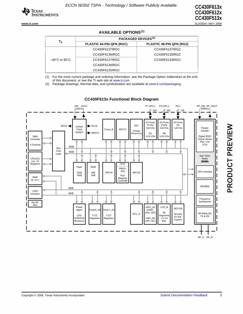
The Texas Instruments CC430 family of ultralow-power microcontroller system-on-chip with integrated RF coresconsists of several devices featuring different sets of peripherals targeted for various applications. Thearchitecture, combined with five low-power modes is optimized to achieve extended battery life in portablemeasurement applications. The device features a powerful 16-bit RISC CPU, 16-bit registers, and constantgenerators that contribute to maximum code efficiency.
The CC430 family provides a tight integration between the microcontroller core, its peripherals, software, and theRF transceiver, making these true system-on-chip solutions easy to use as well as improving performance.
The CC430F61xx series are microcontroller system-on-chip configurations combining the excellent performanceof the state-of-the-art CC1101 <1-GHz RF transceiver with the MSP430 CPUXV2, up to 32 kB of in-systemprogrammable flash memory, up to 4 kB of RAM, two 16-bit timers, a high-performance 12-bit A/D converter witheight external inputs plus internal temperature and battery sensors on CC430F613x devices, comparator,universal serial communication interfaces (USCI), 128-bit AES security accelerator, hardware multiplier, DMA,real-time clock module with alarm capabilities, LCD driver, and up to 44 I/O pins.
The CC430F513x series are microcontroller system-on-chip configurations combining the excellent performanceof the state-of-the-art CC1101 <1-GHz RF transceiver with the MSP430 CPUXV2, up to 32 kB of in-systemprogrammable flash memory, up to 4 kB of RAM, two 16-bit timers, a high performance 12-bit A/D converter witheight external inputs plus internal temperature and battery sensors, comparator, universal serial communicationinterfaces (USCI), 128-bit AES security accelerator, hardware multiplier, DMA, real-time clock module with alarmcapabilities, and up to 32 I/O pins.
Typical applications for these devices include wireless analog and digital sensor systems, heat cost allocators,thermostats, etc.
For complete module descriptions, see the CC430 Family User's Guide, literature number SLAU259.
2 Submit Documentation Feedback Copyright © 2009, Texas Instruments Incorporated
PR
OD
UC
T P
RE
VIE
W
RAM
4kB2kB
Power
Mgmt
LDO
SVM/SVS
Brownout
SYS
Timer0_A5
5 CC
Registers
EEM
(S: 3+1)
RTC_A
Comp_B
Flash
32kB
16kB
SMCLK
ACLK
MDB
MAB
XOUTXIN
Spy-Bi-
Wire
CRC16
Bus
Cntrl
Logic
MAB
MDB
MAB
MDB
MCLK
USCI_A0
(UART,
IrDA, SPI)
USCI_B0
(SPI, I2C)
LCD_B
96
Segments
1,2,3,4
Mux
I/O Ports
P1/P2
2x8 I/Os
PA
1x16 I/Os
P1.x/P2.x
2x8
I/O Ports
P3/P4
2x8 I/Os
PB
1x16 I/Os
P3.x/P4.x
2x8
I/O Ports
P5
1x8 I/Os
P5.x
1x8
AES128
Security
En-/De-
cryption
RF_XOUTRF_XIN
RF_NRF_P
Timer1_A3
3 CC
Registers
MODEM
RF/ANALOG
TX & RX
Frequency
Synthesizer
CPU Interface
Packet
Handler
Digital RSSI
Carrier Sense
PQI / LQI
CCA
Sub-1GHz
Radio
(CC1101)
MPY32
ADC12
(32kHz) (26MHz)
Unified
Clock
System
CPUXV2incl. 16
Registers
JTAG
Interface
DMA
Controller
3 Channel
PortMappingController
Watch-dog
REF
VoltageReference
ECCN 5E002 TSPA - Technology / Software Publicly Available. CC430F613xCC430F612xCC430F513x
www.ti.com ........................................................................................................................................................................................................ SLAS554–MAY 2009
AVAILABLE OPTIONS (1)
PACKAGED DEVICES (2)TA PLASTIC 64-PIN QFN (RGC) PLASTIC 48-PIN QFN (RGZ)
CC430F6137IRGC CC430F5137IRGZCC430F6135IRGC CC430F5135IRGZ
–40°C to 85°C CC430F6127IRGC CC430F5133IRGZCC430F6126IRGCCC430F6125IRGC
(1) For the most current package and ordering information, see the Package Option Addendum at the endof this document, or see the TI web site at www.ti.com.
(2) Package drawings, thermal data, and symbolization are available at www.ti.com/packaging.
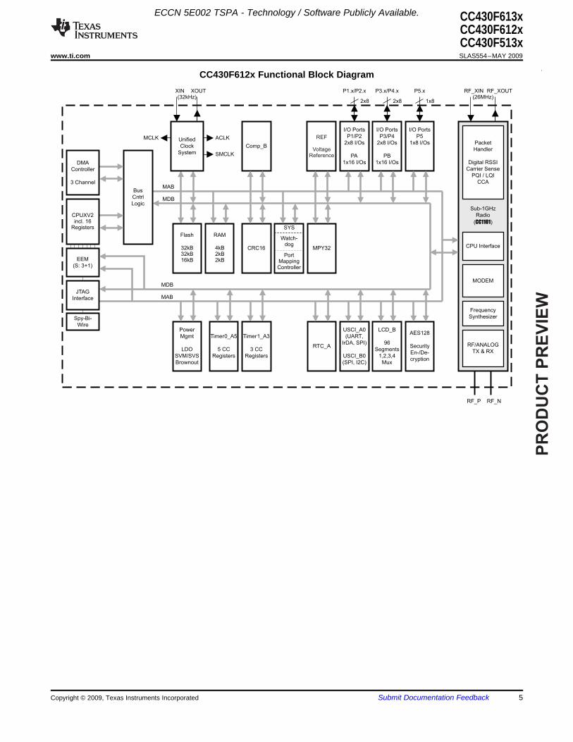
CC430F613x Functional Block Diagram
Copyright © 2009, Texas Instruments Incorporated Submit Documentation Feedback 3
PR
OD
UC
T P
RE
VIE
W
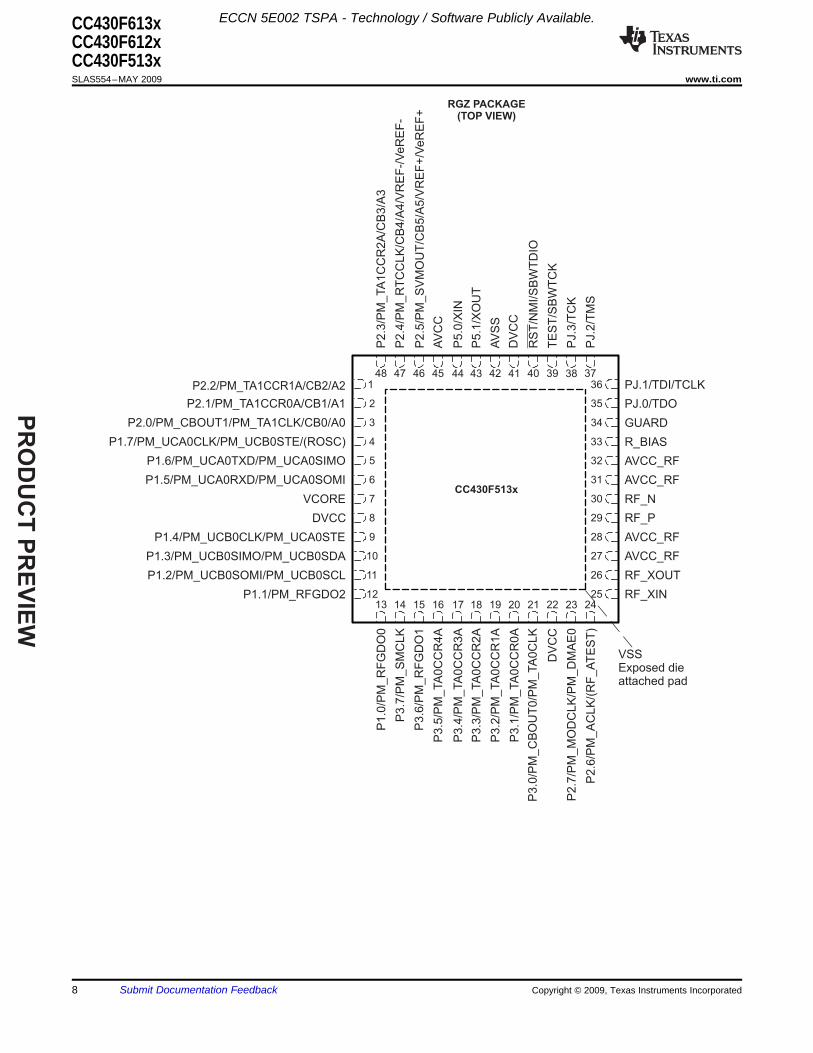
RGC PACKAGE(TOP VIEW)
CC430F613x
P3.7
/PM
_S
MC
LK
/S17
P2.0
/PM
_C
BO
UT
1/P
M_TA
1C
LK
/CB
0/A
0
17
64P
3.6
/PM
_R
FG
DO
1/S
16
P2.1
/PM
_TA
1C
CR
0A
/CB
1/A
1
18
63
P3.5
/PM
_TA
0C
CR
4A
/S15
P2.2
/PM
_TA
1C
CR
1A
/CB
2/A
2
19
62
P2.3
/PM
_TA
1C
CR
2A
/CB
3/A
3P
3.4
/PM
_TA
0C
CR
3A
/S14
20
61
P2.4
/PM
_R
TC
CLK
/CB
4/A
4/V
RE
F-/
VeR
EF
-P
3.3
/PM
_TA
0C
CR
2A
/S13
21
60
P2.5
//C
B5/A
5P
M_S
VM
OU
T/V
RE
F+
/VeR
EF
+P
3.2
/PM
_TA
0C
CR
1A
/S12
22
59
DV
CC
P4.4
/S6
29
52
RS
T/N
MI/S
BW
TD
IOP
4.3
/S5
30
51
TE
ST
/SB
WT
CK
P4.2
/S4
31
50
PJ.3
/TC
KP
4.1
/S3
32
49
P2.6
/PM
_A
CLK
/CB
6/A
6P
3.1
/PM
_TA
0C
CR
0A
/S11
23
58
P2.7
//C
B7/A
7P
M_M
OD
CLK
/PM
_D
MA
E0
P3.0
/PM
_C
BO
UT
0/P
M_TA
0C
LK
/S10
24
57
AV
CC
DV
CC
25
56
P5.0
/XIN
P4.7
/S9
26
55
P5.1
/XO
UT
P4.6
/S8
27
54
AV
SS
P4.5
/S7
28
53
P4.0/S2/(RF_ATEST)P1.0/PM_RFGDO0/S18 3316
P5.3/S1P1.1/PM_RFGDO2/S19 3415
P5.2/S0P1.2/PM_UCB0SOMI/PM_UCB0SCL/S20 3514
RF_XINP1.3/PM_UCB0SIMO/PM_UCB0SDA/S21 3613
RF_XOUTP1.4/PM_UCB0CLK/PM_UCA0STE/S22 3712
AVCC_RFDVCC 3811
GUARDLCDCAP/R33 454
PJ.0/TDOP1.5/PM_UCA0RXD/PM_UCA0SOMI/R23 463
PJ.1/TDI/TCLKP1.6/PM_UCA0TXD/PM_UCA0SIMO/R13/LCDREF 472
PJ.2/TMSP1.7/PM_UCA0CLK/PM_UCB0STE/R03/(ROSC) 481
AVCC_RFVCORE 3910
RF_PP5.4/S23 409
RF_NP5.5/COM3/S24 418
AVCC_RFP5.6/COM2/S25 427
AVCC_RFP5.7/COM1/S26 436
R_BIASCOM0 445
VSSExposed dieattached pad
ECCN 5E002 TSPA - Technology / Software Publicly Available.CC430F613xCC430F612xCC430F513xSLAS554–MAY 2009 ........................................................................................................................................................................................................ www.ti.com
4 Submit Documentation Feedback Copyright © 2009, Texas Instruments Incorporated
PR
OD
UC
T P
RE
VIE
W
RAM
4kB2kB2kB
Power
Mgmt
LDO
SVM/SVS
Brownout
Timer0_A5
5 CC
Registers
EEM
(S: 3+1)
RTC_A
Comp_B
Flash
32kB32kB16kB
SMCLK
ACLK
MDB
MAB
XOUTXIN
Spy-Bi-
Wire
CRC16
Bus
Cntrl
Logic
MAB
MDB
MAB
MDB
MCLK
USCI_A0
(UART,
IrDA, SPI)
USCI_B0
(SPI, I2C)
LCD_B
96
Segments
1,2,3,4
Mux
I/O Ports
P1/P2
2x8 I/Os
PA
1x16 I/Os
P1.x/P2.x
2x8
I/O Ports
P3/P4
2x8 I/Os
PB
1x16 I/Os
P3.x/P4.x
2x8
I/O Ports
P5
1x8 I/Os
P5.x
1x8
AES128
Security
En-/De-
cryption
RF_XOUTRF_XIN
RF_NRF_P
Timer1_A3
3 CC
Registers
MODEM
RF/ANALOG
TX & RX
Frequency
Synthesizer
CPU Interface
Packet
Handler
Digital RSSI
Carrier Sense
PQI / LQI
CCA
Sub-1GHz
Radio
(CC1101)
MPY32
(32kHz) (26MHz)
Unified
Clock
System
JTAG
Interface
DMA
Controller
3 Channel
SYS
PortMappingController
Watch-dog
REF
VoltageReference
CPUXV2incl. 16
Registers
ECCN 5E002 TSPA - Technology / Software Publicly Available. CC430F613xCC430F612xCC430F513x
www.ti.com ........................................................................................................................................................................................................ SLAS554–MAY 2009
CC430F612x Functional Block Diagram
Copyright © 2009, Texas Instruments Incorporated Submit Documentation Feedback 5

PR
OD
UC
T P
RE
VIE
W
RGC PACKAGE(TOP VIEW)
CC430F612x
P3.7
/PM
_S
MC
LK
/S17
P2.0
/PM
_C
BO
UT
1/P
M_TA
1C
LK
/CB
0
17
64P
3.6
/PM
_R
FG
DO
1/S
16
P2.1
/PM
_TA
1C
CR
0A
/CB
1
18
63
P3.5
/PM
_TA
0C
CR
4A
/S15
P2.2
/PM
_TA
1C
CR
1A
/CB
2
19
62
P2.3
/PM
_TA
1C
CR
2A
/CB
3P
3.4
/PM
_TA
0C
CR
3A
/S14
20
61
P2.4
/PM
_R
TC
CLK
/CB
4P
3.3
/PM
_TA
0C
CR
2A
/S13
21
60
P2.5
//C
B5
PM
_S
VM
OU
TP
3.2
/PM
_TA
0C
CR
1A
/S12
22
59
DV
CC
P4.4
/S6
29
52
RS
T/N
MI/S
BW
TD
IOP
4.3
/S5
30
51
TE
ST
/SB
WT
CK
P4.2
/S4
31
50
PJ.3
/TC
KP
4.1
/S3
32
49
P2.6
/PM
_A
CLK
/CB
6P
3.1
/PM
_TA
0C
CR
0A
/S11
23
58
P2.7
//C
BP
M_M
OD
CLK
/PM
_D
MA
E0
P3.0
/PM
_C
BO
UT
0/P
M_TA
0C
LK
/S10
24
57
AV
CC
DV
CC
25
56
P5.0
/XIN
P4.7
/S9
26
55
P5.1
/XO
UT
P4.6
/S8
27
54
AV
SS
P4.5
/S7
28
53
P4.0/S2/(RF_ATEST)P1.0/PM_RFGDO0/S18 3316
P5.3/S1P1.1/PM_RFGDO2/S19 3415
P5.2/S0P1.2/PM_UCB0SOMI/PM_UCB0SCL/S20 3514
RF_XINP1.3/PM_UCB0SIMO/PM_UCB0SDA/S21 3613
RF_XOUTP1.4/PM_UCB0CLK/PM_UCA0STE/S22 3712
AVCC_RFDVCC 3811
GUARDLCDCAP/R33 454
PJ.0/TDOP1.5/PM_UCA0RXD/PM_UCA0SOMI/R23 463
PJ.1/TDI/TCLKP1.6/PM_UCA0TXD/PM_UCA0SIMO/R13/LCDREF 472
PJ.2/TMSP1.7/PM_UCA0CLK/PM_UCB0STE/R03/(ROSC) 481
AVCC_RFVCORE 3910
RF_PP5.4/S23 409
RF_NP5.5/COM3/S24 418
AVCC_RFP5.6/COM2/S25 427
AVCC_RFP5.7/COM1/S26 436
R_BIASCOM0 445
VSSExposed dieattached pad
ECCN 5E002 TSPA - Technology / Software Publicly Available.CC430F613xCC430F612xCC430F513xSLAS554–MAY 2009 ........................................................................................................................................................................................................ www.ti.com
6 Submit Documentation Feedback Copyright © 2009, Texas Instruments Incorporated
PR
OD
UC
T P
RE
VIE
W
RAM
4kB
2kB
Power
Mgmt
LDO
SVM/SVS
Brownout
Timer0_A5
5 CC
Registers
EEM
(S: 3+1)
RTC_A
Comp_B
Flash
32kB16kB8kB
SMCLK
ACLK
MDB
MAB
XOUTXIN
Spy-Bi-
Wire
CRC16
Bus
Cntrl
Logic
MAB
MDB
MAB
MDB
MCLK
USCI_A0
(UART,
IrDA, SPI)
USCI_B0
(SPI, I2C)
I/O Ports
P1/P2
2x8 I/Os
PA
1x16 I/Os
P1.x/P2.x
2x8
I/O Ports
P3
1x8 I/Os
P3.x
1x8
I/O Ports
P5
1x2 I/Os
P5.x
1x2
AES128
Security
En-/De-
cryption
RF_XOUTRF_XIN
RF_NRF_P
Timer1_A3
3 CC
Registers
MODEM
RF/ANALOG
TX & RX
Frequency
Synthesizer
CPU Interface
Packet
Handler
Digital RSSI
Carrier Sense
PQI / LQI
CCA
Sub-1GHz
Radio
(CC1101)
MPY32
ADC12
(32kHz) (26MHz)
Unified
Clock
System
JTAG
Interface
DMA
Controller
3 Channel
SYS
PortMappingController
Watch-dog
REF
VoltageReference
CPUXV2incl. 16
Registers
ECCN 5E002 TSPA - Technology / Software Publicly Available. CC430F613xCC430F612xCC430F513x
www.ti.com ........................................................................................................................................................................................................ SLAS554–MAY 2009
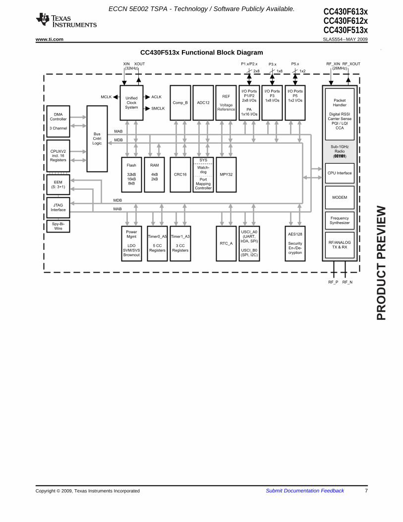
CC430F513x Functional Block Diagram
Copyright © 2009, Texas Instruments Incorporated Submit Documentation Feedback 7
PR
OD
UC
T P
RE
VIE
W
RGZ PACKAGE(TOP VIEW)
12
11
4
3
2
1
10
9
8
7
6
5
13 14 15 16 17 18 19 20 21 22 23 2425
26
27
28
29
30
31
32
33
34
35
3648 47 46 45 44 43 42 41 40 39 38 37
P1.1/PM_RFGDO2
P1.2/PM_UCB0SOMI/PM_UCB0SCL
P1.7/PM_UCA0CLK/PM_UCB0STE/(ROSC)
P2.0/PM_CBOUT1/PM_TA1CLK/CB0/A0
P2.1/PM_TA1CCR0A/CB1/A1
P2.2/PM_TA1CCR1A/CB2/A2
P1.3/PM_UCB0SIMO/PM_UCB0SDA
P1.4/PM_UCB0CLK/PM_UCA0STE
DVCC
VCORE
P1.5/PM_UCA0RXD/PM_UCA0SOMI
P1.6/PM_UCA0TXD/PM_UCA0SIMO
RF_XIN
RF_XOUT
AVCC_RF
GUARD
PJ.0/TDO
PJ.1/TDI/TCLK
AVCC_RF
RF_P
RF_N
AVCC_RF
AVCC_RF
R_BIAS
P2.3
/PM
_TA
1C
CR
2A
/CB
3/A
3
P2.4
/PM
_R
TC
CLK
/CB
4/A
4/V
RE
F-/
VeR
EF
-
RS
T/N
MI/S
BW
TD
IO
TE
ST
/SB
WT
CK
PJ.3
/TC
K
PJ.2
/TM
S
P2.5
/PM
_S
VM
OU
T/C
B5/A
5/V
RE
F+
/VeR
EF
+
AV
CC
P5.0
/XIN
P5.1
/XO
UT
AV
SS
DV
CC
P1.0
/PM
_R
FG
DO
0
P3.7
/PM
_S
MC
LK
P3.6
/PM
_R
FG
DO
1
P3.5
/PM
_TA
0C
CR
4A
P3.4
/PM
_TA
0C
CR
3A
P3.3
/PM
_TA
0C
CR
2A
P3.2
/PM
_TA
0C
CR
1A
P3.1
/PM
_TA
0C
CR
0A
P3.0
/PM
_C
BO
UT
0/P
M_TA
0C
LK
DV
CC
P2.7
/PM
_M
OD
CLK
/PM
_D
MA
E0
P2.6
/PM
_A
CLK
/(R
F_A
TE
ST
)
VSSExposed dieattached pad
CC430F513x
ECCN 5E002 TSPA - Technology / Software Publicly Available.CC430F613xCC430F612xCC430F513xSLAS554–MAY 2009 ........................................................................................................................................................................................................ www.ti.com
8 Submit Documentation Feedback Copyright © 2009, Texas Instruments Incorporated
PR
OD
UC
T P
RE
VIE
W
ECCN 5E002 TSPA - Technology / Software Publicly Available. CC430F613xCC430F612xCC430F513x
www.ti.com ........................................................................................................................................................................................................ SLAS554–MAY 2009
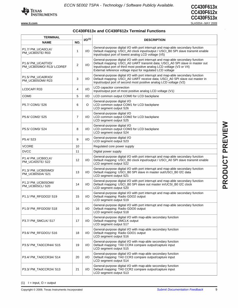
CC430F613x and CC430F612x Terminal FunctionsTERMINAL
I/O (1) DESCRIPTIONNAME NO.
General-purpose digital I/O with port interrupt and map-able secondary functionP1.7/ PM_UCA0CLK/ 1 I/O Default mapping: USCI_A0 clock input/output / USCI_B0 SPI slave transmit enablePM_UCB0STE/ R03 Input/output port of lowest analog LCD voltage (V5)General-purpose digital I/O with port interrupt and map-able secondary function
P1.6/ PM_UCA0TXD/ Default mapping: USCI_A0 UART transmit data; USCI_A0 SPI slave in master out2 I/OPM_UCB0SIMO/ R13/ LCDREF Input/output port of third most positive analog LCD voltage (V3 or V4)External reference voltage input for regulated LCD voltageGeneral-purpose digital I/O with port interrupt and map-able secondary functionP1.5/ PM_UCA0RXD/ 3 I/O Default mapping: USCI_A0 UART receive data; USCI_A0 SPI slave out master inPM_UCB0SOMI/ R23 Input/output port of second most positive analog LCD voltage (V2)LCD capacitor connectionLCDCAP/ R33 4 I/O Input/output port of most positive analog LCD voltage (V1)
COM0 5 I/O LCD common output COM0 for LCD backplaneGeneral-purpose digital I/O
P5.7/ COM1/ S26 6 O LCD common output COM1 for LCD backplaneLCD segment output S26General-purpose digital I/O
P5.6/ COM2/ S25 7 I/O LCD common output COM2 for LCD backplaneLCD segment output S25General-purpose digital I/O
P5.5/ COM3/ S24 8 I/O LCD common output COM3 for LCD backplaneLCD segment output S24General-purpose digital I/OP5.4/ S23 9 I/O LCD segment output S23
VCORE 10 Regulated core power supplyDVCC 11 Digital power supply
General-purpose digital I/O with port interrupt and map-able secondary functionP1.4/ PM_UCB0CLK/ 12 I/O Default mapping: USCI_B0 clock input/output / USCI_A0 SPI slave transmit enablePM_UCA0STE/ S22 LCD segment output S22General-purpose digital I/O with port interrupt and map-able secondary functionP1.3/ PM_UCB0SIMO/ 13 I/O Default mapping: USCI_B0 SPI slave in master out/USCI_B0 I2C dataPM_UCB0SDA/ S21 LCD segment output S21General-purpose digital I/O with port interrupt and map-able secondary functionP1.2/ PM_UCB0SOMI/ 14 I/O Default mapping: USCI_B0 SPI slave out master in/UCSI_B0 I2C clockPM_UCB0SCL/ S20 LCD segment output S20General-purpose digital I/O with port interrupt and map-able secondary function
P1.1/ PM_RFGDO2/ S19 15 I/O Default mapping: Radio GDO2 outputLCD segment output S19General-purpose digital I/O with port interrupt and map-able secondary function
P1.0/ PM_RFGDO0/ S18 16 I/O Default mapping: Radio GDO0 outputLCD segment output S18General-purpose digital I/O with map-able secondary function
P3.7/ PM_SMCLK/ S17 17 I/O Default mapping: SMCLK outputLCD segment output S17General-purpose digital I/O with map-able secondary function
P3.6/ PM_RFGDO1/ S16 18 I/O Default mapping: Radio GDO1 outputLCD segment output S16General-purpose digital I/O with map-able secondary function
P3.5/ PM_TA0CCR4A/ S15 19 I/O Default mapping: TA0 CCR4 compare output/capture inputLCD segment output S15General-purpose digital I/O with map-able secondary function
P3.4/ PM_TA0CCR3A/ S14 20 I/O Default mapping: TA0 CCR3 compare output/capture inputLCD segment output S14General-purpose digital I/O with map-able secondary function
P3.3/ PM_TA0CCR2A/ S13 21 I/O Default mapping: TA0 CCR2 compare output/capture inputLCD segment output S13
(1) I = input, O = output
Copyright © 2009, Texas Instruments Incorporated Submit Documentation Feedback 9
PR
OD
UC
T P
RE
VIE
W
ECCN 5E002 TSPA - Technology / Software Publicly Available.CC430F613xCC430F612xCC430F513xSLAS554–MAY 2009 ........................................................................................................................................................................................................ www.ti.com
CC430F613x and CC430F612x Terminal Functions (continued)TERMINAL
I/O (1) DESCRIPTIONNAME NO.
General-purpose digital I/O with map-able secondary functionP3.2/ PM_TA0CCR1A/ S12 22 I/O Default mapping: TA0 CCR1 compare output/capture input
LCD segment output S12General-purpose digital I/O with map-able secondary function
P3.1/ PM_TA0CCR0A/ S11 23 I/O Default mapping: TA0 CCR0 compare output/capture inputLCD segment output S11General-purpose digital I/O with map-able secondary functionP3.0/ PM_CBOUT0/ PM_TA0CLK/ 24 I/O Default mapping: Comparator_B output; Timer0_A5 clock inputS10 LCD segment output S10
DVCC 25 Digital power supplyGeneral-purpose digital I/OP4.7/ S9 26 I/O LCD segment output S9General-purpose digital I/OP4.6/ S8 27 I/O LCD segment output S8General-purpose digital I/OP4.5/ S7 28 I/O LCD segment output S7General-purpose digital I/OP4.4/ S6 29 I/O LCD segment output S6General-purpose digital I/OP4.3/ S5 30 I/O LCD segment output S5General-purpose digital I/OP4.2/ S4 31 I/O LCD segment output S4General-purpose digital I/OP4.1/ S3 32 I/O LCD segment output S3General-purpose digital I/OP4.0/ S2 33 I/O LCD segment output S2General-purpose digital I/OP5.3/ S1 34 I/O LCD segment output S1General-purpose digital I/OP5.2/ S0 35 I/O LCD segment output S0
RF_XIN 36 I Input terminal for RF crystal oscillator, or external clock inputRF_XOUT 37 O Output terminal for RF crystal oscillatorAVCC_RF 38 Radio analog power supplyAVCC_RF 39 Radio analog power supply
RF Positive RF input to LNA in receive modeRF_P 40 I/O Positive RF output from PA in transmit modeRF Negative RF input to LNA in receive modeRF_N 41 I/O Negative RF output from PA in transmit mode
AVCC_RF 42 Radio analog power supplyAVCC_RF 43 Radio analog power supplyRBIAS 44 External bias resistor for radio reference currentGUARD 45 Power supply connection for digital noise isolation
General-purpose digital I/OPJ.0/ TDO 46 I/O Test data output portGeneral-purpose digital I/OPJ.1/ TDI/ TCLK 47 I/O Test data input or test clock inputGeneral-purpose digital I/OPJ.2/ TMS 48 I/O Test mode selectGeneral-purpose digital I/OPJ.3/ TCK 49 I/O Test clockTest mode pin – select digital I/O on JTAG pinsTEST/ SBWTCK 50 I Spy-bi-wire input clock
10 Submit Documentation Feedback Copyright © 2009, Texas Instruments Incorporated
PR
OD
UC
T P
RE
VIE
W
ECCN 5E002 TSPA - Technology / Software Publicly Available. CC430F613xCC430F612xCC430F513x
www.ti.com ........................................................................................................................................................................................................ SLAS554–MAY 2009
CC430F613x and CC430F612x Terminal Functions (continued)TERMINAL
I/O (1) DESCRIPTIONNAME NO.
Reset input active lowRST/NMI/ SBWTDIO 51 I/O Non-maskable interrupt input
Spy-bi-wire data input/outputDVCC 52 Digital power supplyAVSS 53 Analog ground supply for ADC12
General-purpose digital I/OP5.1/ XOUT 54 I/O Output terminal of crystal oscillator XT1General-purpose digital I/OP5.0/ XIN 55 I/O Input terminal for crystal oscillator XT1
AVCC 56 Analog power supplyGeneral-purpose digital I/O with port interrupt and map-able secondary function
P2.7/ PM_ADC12CLK/ Default mapping: ADC12CLK output; DMA external trigger input57 I/OPM_DMAE0/ CB7 (/A7) Comparator_B input CB7Analog input A7 – 12-bit ADC (only CC430F613x)General-purpose digital I/O with port interrupt and map-able secondary functionDefault mapping: ACLK outputP2.6/ PM_ACLK/ CB6 (/A6) 58 I/O Comparator_B input CB6Analog input A6 – 12-bit ADC (only CC430F613x)General-purpose digital I/O with port interrupt and map-able secondary functionDefault mapping: SVM output
P2.5/ PM_SVMOUT/ CB5 Comparator_B input CB559 I/O(/A5/ VREF+/ VeREF+) Analog input A5 – 12-bit ADC (only CC430F613x)Output of reference voltage to the ADC (only CC430F613x)Input for an external reference voltage to the ADC (only CC430F613x)General-purpose digital I/O with port interrupt and map-able secondary functionDefault mapping: RTCCLK output
P2.4/ PM_RTCCLK/ CB4 Comparator_B input CB460 I/O(/A4/ VREF-/ VeREF-) Analog input A4 – 12-bit ADC (only CC430F613x)Negative terminal for the ADC's reference voltage for both sources, the internalreference voltage, or an external applied reference voltage (only CC430F613x)General-purpose digital I/O with port interrupt and map-able secondary functionDefault mapping: TA1 CCR2 compare output/capture inputP2.3/ PM_TA1CCR2A/ CB3 (/A3) 61 I/O Comparator_B input CB3Analog input A3 – 12-bit ADC (only CC430F613x)General-purpose digital I/O with port interrupt and map-able secondary functionDefault mapping: TA1 CCR1 compare output/capture inputP2.2/ PM_TA1CCR1A/ CB2 (/A2) 62 I/O Comparator_B input CB2Analog input A2 – 12-bit ADC (only CC430F613x)General-purpose digital I/O with port interrupt and map-able secondary functionDefault mapping: TA1 CCR0 compare output/capture inputP2.1/PM_TA1CCR0A/CB1(/A1) 63 I/O Comparator_B input CB1Analog input A1 – 12-bit ADC (only CC430F613x)General-purpose digital I/O with port interrupt and map-able secondary function
P2.0/ PM_CBOUT1/ PM_TA1CLK/ Default mapping: Comparator_B output; Timer1_A3 clock input64 I/OCB0 (/A0) Comparator_B input CB0Analog input A0 – 12-bit ADC (only CC430F613x)Ground supply
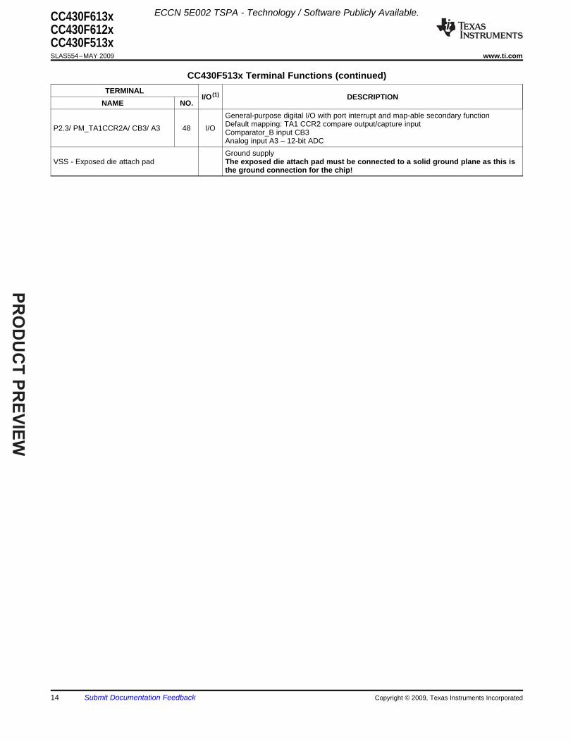
VSS - Exposed die attach pad The exposed die attach pad must be connected to a solid ground plane as this isthe ground connection for the chip!
Copyright © 2009, Texas Instruments Incorporated Submit Documentation Feedback 11
PR
OD
UC
T P
RE
VIE
W
ECCN 5E002 TSPA - Technology / Software Publicly Available.CC430F613xCC430F612xCC430F513xSLAS554–MAY 2009 ........................................................................................................................................................................................................ www.ti.com
CC430F513x Terminal FunctionsTERMINAL
I/O (1) DESCRIPTIONNAME NO.
General-purpose digital I/O with port interrupt and map-able secondary functionDefault mapping: TA1 CCR1 compare output/capture inputP2.2/ PM_TA1CCR1A/ CB2/ A2 1 I/O Comparator_B input CB2Analog input A2 – 12-bit ADCGeneral-purpose digital I/O with port interrupt and map-able secondary functionDefault mapping: TA1 CCR0 compare output/capture inputP2.1/ PM_TA1CCR0A/ CB1/ A1 2 I/O Comparator_B input CB1Analog input A1 – 12-bit ADCGeneral-purpose digital I/O with port interrupt and map-able secondary function
P2.0/ PM_CBOUT1/ PM_TA1CLK/ Default mapping: Comparator_B output; Timer1_A3 clock input3 I/OCB0/ A0 Comparator_B input CB0Analog input A0 – 12-bit ADC
P1.7/ PM_UCA0CLK/ General-purpose digital I/O with port interrupt and map-able secondary function4 I/OPM_UCB0STE Default mapping: USCI_A0 clock input/output / USCI_B0 SPI slave transmit enableP1.6/ PM_UCA0TXD/ General-purpose digital I/O with port interrupt and map-able secondary function5 I/OPM_UCB0SIMO Default mapping: USCI_A0 UART transmit data; USCI_A0 SPI slave in master outP1.5/ PM_UCA0RXD/ General-purpose digital I/O with port interrupt and map-able secondary function6 I/OPM_UCB0SOMI Default mapping: USCI_A0 UART receive data; USCI_A0 SPI slave out master inVCORE 7 Regulated core power supplyDVCC 8 Digital power supply
General-purpose digital I/O with port interrupt and map-able secondary functionP1.4/ PM_UCB0CLK/ 9 I/O Default mapping: USCI_B0 clock input/output / USCI_A0 SPI slave transmit enablePM_UCA0STE/ S22 LCD segment output S22General-purpose digital I/O with port interrupt and map-able secondary functionP1.3/ PM_UCB0SIMO/ 10 I/O Default mapping: USCI_B0 SPI slave in master out/USCI_B0 I2C dataPM_UCB0SDA/ S21 LCD segment output S21General-purpose digital I/O with port interrupt and map-able secondary functionP1.2/ PM_UCB0SOMI/ 11 I/O Default mapping: USCI_B0 SPI slave out master in/UCSI_B0 I2C clockPM_UCB0SCL/ S20 LCD segment output S20General-purpose digital I/O with port interrupt and map-able secondary function
P1.1/ PM_RFGDO2/ S19 12 I/O Default mapping: Radio GDO2 outputLCD segment output S19General-purpose digital I/O with port interrupt and map-able secondary function
P1.0/ PM_RFGDO0/ S18 13 I/O Default mapping: Radio GDO0 outputLCD segment output S18General-purpose digital I/O with map-able secondary function
P3.7/ PM_SMCLK/ S17 14 I/O Default mapping: SMCLK outputLCD segment output S17General-purpose digital I/O with map-able secondary function
P3.6/ PM_RFGDO1/ S16 15 I/O Default mapping: Radio GDO1 outputLCD segment output S16General-purpose digital I/O with map-able secondary function
P3.5/ PM_TA0CCR4A/ S15 16 I/O Default mapping: TA0 CCR4 compare output/capture inputLCD segment output S15General-purpose digital I/O with map-able secondary function
P3.4/ PM_TA0CCR3A/ S14 17 I/O Default mapping: TA0 CCR3 compare output/capture inputLCD segment output S14General-purpose digital I/O with map-able secondary function
P3.3/ PM_TA0CCR2A/ S13 18 I/O Default mapping: TA0 CCR2 compare output/capture inputLCD segment output S13General-purpose digital I/O with map-able secondary function
P3.2/ PM_TA0CCR1A/ S12 19 I/O Default mapping: TA0 CCR1 compare output/capture inputLCD segment output S12General-purpose digital I/O with map-able secondary function
P3.1/ PM_TA0CCR0A/ S11 20 I/O Default mapping: TA0 CCR0 compare output/capture inputLCD segment output S11
(1) I = input, O = output
12 Submit Documentation Feedback Copyright © 2009, Texas Instruments Incorporated
PR
OD
UC
T P
RE
VIE
W
ECCN 5E002 TSPA - Technology / Software Publicly Available. CC430F613xCC430F612xCC430F513x
www.ti.com ........................................................................................................................................................................................................ SLAS554–MAY 2009
CC430F513x Terminal Functions (continued)TERMINAL
I/O (1) DESCRIPTIONNAME NO.
General-purpose digital I/O with map-able secondary functionP3.0/ PM_CBOUT0/ PM_TA0CLK/ 21 I/O Default mapping: Comparator_B output; Timer0_A5 clock inputS10 LCD segment output S10DVCC 22 Digital power supplyP2.7/ PM_ADC12CLK/ General-purpose digital I/O with port interrupt and map-able secondary function23 I/OPM_DMAE0 Default mapping: ADC12CLK output; DMA external trigger input
General-purpose digital I/O with port interrupt and map-able secondary functionP2.6/ PM_ACLK 24 I/O Default mapping: ACLK outputRF_XIN 25 I Input terminal for RF crystal oscillator, or external clock inputRF_XOUT 26 O Output terminal for RF crystal oscillatorAVCC_RF 27 Radio analog power supplyAVCC_RF 28 Radio analog power supply
RF Positive RF input to LNA in receive modeRF_P 29 I/O Positive RF output from PA in transmit modeRF Negative RF input to LNA in receive modeRF_N 30 I/O Negative RF output from PA in transmit mode
AVCC_RF 31 Radio analog power supplyAVCC_RF 32 Radio analog power supplyRBIAS 33 External bias resistor for radio reference currentGUARD 34 Power supply connection for digital noise isolation
General-purpose digital I/OPJ.0/ TDO 35 I/O Test data output portGeneral-purpose digital I/OPJ.1/ TDI/ TCLK 36 I/O Test data input or test clock inputGeneral-purpose digital I/OPJ.2/ TMS 37 I/O Test mode selectGeneral-purpose digital I/OPJ.3/ TCK 38 I/O Test clockTest mode pin – select digital I/O on JTAG pinsTEST/ SBWTCK 39 I Spy-bi-wire input clockReset input active low
RST/NMI/ SBWTDIO 40 I/O Non-maskable interrupt inputSpy-bi-wire data input/output
DVCC 41 Digital power supplyAVSS 42 Analog ground supply for ADC12
General-purpose digital I/OP5.1/ XOUT 43 I/O Output terminal of crystal oscillator XT1General-purpose digital I/OP5.0/ XIN 44 I/O Input terminal for crystal oscillator XT1
AVCC 45 Analog power supplyGeneral-purpose digital I/O with port interrupt and map-able secondary functionDefault mapping: SVM output
P2.5/ PM_SVMOUT/ CB5/ Comparator_B input CB546 I/OA5/ VREF+/ VeREF+ Analog input A5 – 12-bit ADCOutput of reference voltage to the ADCInput for an external reference voltage to the ADCGeneral-purpose digital I/O with port interrupt and map-able secondary functionDefault mapping: RTCCLK output
P2.4/ PM_RTCCLK/ CB4/ Comparator_B input CB447 I/OA4/ VREF-/ VeREF- Analog input A4 – 12-bit ADCNegative terminal for the ADC's reference voltage for both sources, the internalreference voltage, or an external applied reference voltage
Copyright © 2009, Texas Instruments Incorporated Submit Documentation Feedback 13
PR
OD
UC
T P
RE
VIE
W
ECCN 5E002 TSPA - Technology / Software Publicly Available.CC430F613xCC430F612xCC430F513xSLAS554–MAY 2009 ........................................................................................................................................................................................................ www.ti.com
CC430F513x Terminal Functions (continued)TERMINAL
I/O (1) DESCRIPTIONNAME NO.
General-purpose digital I/O with port interrupt and map-able secondary functionDefault mapping: TA1 CCR2 compare output/capture inputP2.3/ PM_TA1CCR2A/ CB3/ A3 48 I/O Comparator_B input CB3Analog input A3 – 12-bit ADCGround supply
VSS - Exposed die attach pad The exposed die attach pad must be connected to a solid ground plane as this isthe ground connection for the chip!
14 Submit Documentation Feedback Copyright © 2009, Texas Instruments Incorporated
PR
OD
UC
T P
RE
VIE
W
SHORT-FORM DESCRIPTION
Sub-1 GHz Radio
BIAS
PA
RBIAS RF_XIN RF_XOUT
XOSC
LNA
0
90
FREQ
SYNTH
ADC
DE
MO
DU
LA
TO
R
PA
CK
ET
HA
ND
LE
R
RX
FIF
OT
XF
IFO
INT
ER
FA
CE
TO
MC
U
RADIO CONTROL
RF_P
RF_N
RC OSC
ADC
MO
DU
LA
TO
R
ECCN 5E002 TSPA - Technology / Software Publicly Available. CC430F613xCC430F612xCC430F513x
www.ti.com ........................................................................................................................................................................................................ SLAS554–MAY 2009
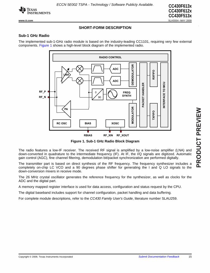
The implemented sub-1-GHz radio module is based on the industry-leading CC1101, requiring very few externalcomponents. Figure 1 shows a high-level block diagram of the implemented radio.
Figure 1. Sub-1 GHz Radio Block Diagram
The radio features a low-IF receiver. The received RF signal is amplified by a low-noise amplifier (LNA) anddown-converted in quadrature to the intermediate frequency (IF). At IF, the I/Q signals are digitized. Automaticgain control (AGC), fine channel filtering, demodulation bit/packet synchronization are performed digitally.
The transmitter part is based on direct synthesis of the RF frequency. The frequency synthesizer includes acompletely on-chip LC VCO and a 90 degrees phase shifter for generating the I and Q LO signals to thedown-conversion mixers in receive mode.
The 26 MHz crystal oscillator generates the reference frequency for the synthesizer, as well as clocks for theADC and the digital part.
A memory mapped register interface is used for data access, configuration and status request by the CPU.
The digital baseband includes support for channel configuration, packet handling and data buffering.
For complete module descriptions, refer to the CC430 Family User's Guide, literature number SLAU259.
Copyright © 2009, Texas Instruments Incorporated Submit Documentation Feedback 15
PR
OD
UC
T P
RE
VIE
W
CPU
Operating Modes
ECCN 5E002 TSPA - Technology / Software Publicly Available.CC430F613xCC430F612xCC430F513xSLAS554–MAY 2009 ........................................................................................................................................................................................................ www.ti.com
The MSP430 CPU has a 16-bit RISC architecture that is highly transparent to the application. All operations,other than program-flow instructions, are performed as register operations in conjunction with seven addressingmodes for source operand and four addressing modes for destination operand.
The CPU is integrated with 16 registers that provide reduced instruction execution time. The register-to-registeroperation execution time is one cycle of the CPU clock.
Four of the registers, R0 to R3, are dedicated as program counter, stack pointer, status register, and constantgenerator, respectively. The remaining registers are general-purpose registers.
Peripherals are connected to the CPU using data, address, and control buses, and can be handled with allinstructions.
The instruction set consists of the original 51 instructions with three formats and seven address modes andadditional instructions for the expanded address range. Each instruction can operate on word and byte data.
The MSP430 has one active mode and six software selectable low-power modes of operation. An interrupt eventcan wake up the device from any of the five low-power modes, service the request, and restore back to thelow-power mode on return from the interrupt program.
The following seven operating modes can be configured by software:• Active mode (AM)
– All clocks are active• Low-power mode 0 (LPM0)
– CPU is disabled– ACLK and SMCLK remain active, MCLK is disabled– FLL loop control remains active
• Low-power mode 1 (LPM1)– CPU is disabled– FLL loop control is disabled– ACLK and SMCLK remain active, MCLK is disabled
• Low-power mode 2 (LPM2)– CPU is disabled– MCLK and FLL loop control and DCOCLK are disabled– DCO's dc-generator remains enabled– ACLK remains active
• Low-power mode 3 (LPM3)– CPU is disabled– MCLK, FLL loop control, and DCOCLK are disabled– DCO's dc-generator is disabled– ACLK remains active
• Low-power mode 4 (LPM4)– CPU is disabled– ACLK is disabled– MCLK, FLL loop control, and DCOCLK are disabled– DCO's dc-generator is disabled– Crystal oscillator is stopped– Complete data retention
16 Submit Documentation Feedback Copyright © 2009, Texas Instruments Incorporated
PR
OD
UC
T P
RE
VIE
W
Interrupt Vector Addresses
ECCN 5E002 TSPA - Technology / Software Publicly Available. CC430F613xCC430F612xCC430F513x
www.ti.com ........................................................................................................................................................................................................ SLAS554–MAY 2009
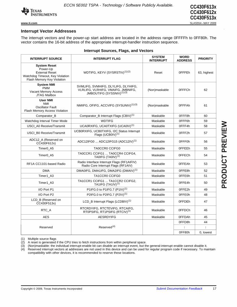
The interrupt vectors and the power-up start address are located in the address range 0FFFFh to 0FF80h. Thevector contains the 16-bit address of the appropriate interrupt-handler instruction sequence.
Interrupt Sources, Flags, and VectorsSYSTEM WORDINTERRUPT SOURCE INTERRUPT FLAG PRIORITYINTERRUPT ADDRESS
System ResetPower-Up
External Reset WDTIFG, KEYV (SYSRSTIV) (1) (2) Reset 0FFFEh 63, highestWatchdog Timeout, Key Violation
Flash Memory Key ViolationSystem NMI SVMLIFG, SVMHIFG, DLYLIFG, DLYHIFG,PMM VLRLIFG, VLRHIFG, VMAIFG, JMBNIFG, (Non)maskable 0FFFCh 62Vacant Memory Access JMBOUTIFG (SYSSNIV) (1) (3)
JTAG MailboxUser NMI
NMI NMIIFG, OFIFG, ACCVIFG (SYSUNIV) (1) (3) (Non)maskable 0FFFAh 61Oscillator FaultFlash Memory Access Violation
Comparator_B Comparator_B Interrupt Flags (CBIV) (1) Maskable 0FFF8h 60Watchdog Interval Timer Mode WDTIFG Maskable 0FFF6h 59
USCI_A0 Receive/Transmit UCA0RXIFG, UCA0TXIFG (UCA0IV) (1) Maskable 0FFF4h 58UCB0RXIFG, UCB0TXIFG, I2C Status InterruptUSCI_B0 Receive/Transmit Maskable 0FFF2h 57Flags (UCB0IV) (1)
ADC12_A (Reserved on ADC12IFG0 ... ADC12IFG15 (ADC12IV) (1) Maskable 0FFF0h 56CC430F612x)Timer0_A5 TA0CCR0 CCIFG0 Maskable 0FFEEh 55
TA0CCR1 CCIFG1 ... TA0CCR4 CCIFG4,Timer0_A5 Maskable 0FFECh 54TA0IFG (TA0IV) (1)
Radio Interface Interrupt Flags (RF1AIFIV)RF1A CC1101-based Radio Maskable 0FFEAh 53Radio Core Interrupt Flags (RF1AIV)DMA DMA0IFG, DMA1IFG, DMA2IFG (DMAIV) (1) Maskable 0FFE8h 52
Timer1_A3 TA1CCR0 CCIFG0 Maskable 0FFE6h 51TA1CCR1 CCIFG1 ... TA1CCR2 CCIFG2,Timer1_A3 Maskable 0FFE4h 50TA1IFG (TA1IV) (1)
I/O Port P1 P1IFG.0 to P1IFG.7 (P1IV) (1) Maskable 0FFE2h 49I/O Port P2 P2IFG.0 to P2IFG.7 (P2IV) (1) Maskable 0FFE0h 48
LCD_B (Reserved on LCD_B Interrupt Flags (LCDBIV) (1) Maskable 0FFDEh 47CC430F513x)RTCRDYIFG, RTCTEVIFG, RTCAIFG,RTC_A Maskable 0FFDCh 46RT0PSIFG, RT1PSIFG (RTCIV) (1)
AES AESRDYIFG Maskable 0FFDAh 450FFD8h 44
Reserved Reserved (4) ⋮ ⋮0FF80h 0, lowest
(1) Multiple source flags(2) A reset is generated if the CPU tries to fetch instructions from within peripheral space.(3) (Non)maskable: the individual interrupt-enable bit can disable an interrupt event, but the general-interrupt enable cannot disable it.(4) Reserved interrupt vectors at addresses are not used in this device and can be used for regular program code if necessary. To maintain
compatibility with other devices, it is recommended to reserve these locations.
Copyright © 2009, Texas Instruments Incorporated Submit Documentation Feedback 17
PR
OD
UC
T P
RE
VIE
W
Memory Organization
Bootstrap Loader (BSL)
Flash Memory
ECCN 5E002 TSPA - Technology / Software Publicly Available.CC430F613xCC430F612xCC430F513xSLAS554–MAY 2009 ........................................................................................................................................................................................................ www.ti.com
Memory OrganizationCC430F6137/F6127/F513 CC430F6135/F6125/F512CC430F6126 (1) CC430F5123 (1)
7 (1) 5 (1)
Main Memory Main 32kB 32kB 16kB 8kB(flash) 00FFFFh–00FF80h 00FFFFh–00FF80h 00FFFFh–00FF80h 00FFFFh–00FF80hMain: interrupt 00FFFFh–008000h 00FFFFh–008000h 00FFFFh–00C000h 00FFFFh–00E000hvectorMain: codememory
Sect 1 2kB not available not available not availableRAM 002BFFh–002400h (2kB)Sect 0 2kB 2kB 2kB 2kB
0023FFh–001C00h (2kB) 0023FFh–001C00h (2kB) 0023FFh–001C00h (2kB) 0023FFh–001C00h (2kB)C 128 B 128 B 128 B 128 B
TLV (Device 001AFFh to 001A80h 001AFFh to 001A80h 001AFFh to 001A80h 001AFFh to 001A80hDescriptor)
D 128 B 128 B 128 B 128 BStructures001A7Fh to 001A00h 001A7Fh to 001A00h 001A7Fh to 001A00h 001A7Fh to 001A00h
Info A 128 B 128 B 128 B 128 B0019FFh to 001980h 0019FFh to 001980h 0019FFh to 001980h 0019FFh to 001980h
Info B 128 B 128 B 128 B 128 B00197Fh to 001900h 00197Fh to 001900h 00197Fh to 001900h 00197Fh to 001900hInformation
memory (flash) Info C 128 B 128 B 128 B 128 B0018FFh to 001880h 0018FFh to 001880h 0018FFh to 001880h 0018FFh to 001880h
Info D 128 B 128 B 128 B 128 B00187Fh to 001800h 00187Fh to 001800h 00187Fh to 001800h 00187Fh to 001800h
BSL 3 512 B 512 B 512 B 512 B0017FFh to 001600h 0017FFh to 001600h 0017FFh to 001600h 0017FFh to 001600h
BSL 2 512 B 512 B 512 B 512 BBootstrap loader 0015FFh to 001400h 0015FFh to 001400h 0015FFh to 001400h 0015FFh to 001400h(BSL) memory
BSL 1 512 B 512 B 512 B 512 B(flash)0013FFh to 001200h 0013FFh to 001200h 0013FFh to 001200h 0013FFh to 001200h
BSL 0 512 B 512 B 512 B 512 B0011FFh to 001000h 0011FFh to 001000h 0011FFh to 001000h 0011FFh to 001000h
4 KB 4 KB 4 KB 4 KBPeripherals 000FFFh to 0h 000FFFh to 0h 000FFFh to 0h 000FFFh to 0h
(1) All not mentioned memory regions are vacant memory and any access to them will cause a Vacant Memory Interrupt.
The BSL enables users to program the flash memory or RAM using a UART serial interface. Access to thedevice memory via the BSL is protected by user-defined password. For complete description of the features ofthe BSL and its implementation, see the application report Features of the MSP430F5xx Bootstrap Loader, TIliterature number SLAA400.
Table 1. BSL FunctionsBSL FUNCTION DEVICE OUTPUT SIGNAL
Data transmit P1.6Data receive P1.5
The flash memory can be programmed via the JTAG port, Spy-Bi-Wire (SBW), or in-system by the CPU. TheCPU can perform single-byte, single-word, and long-word writes to the flash memory. Features of the flashmemory include:• Flash memory has n segments of main memory and four segments of information memory (Info A to Info D)
of 128 bytes each. Each segment in main memory is 512 bytes in size.
18 Submit Documentation Feedback Copyright © 2009, Texas Instruments Incorporated
PR
OD
UC
T P
RE
VIE
W
RAM Memory
ECCN 5E002 TSPA - Technology / Software Publicly Available. CC430F613xCC430F612xCC430F513x
www.ti.com ........................................................................................................................................................................................................ SLAS554–MAY 2009
• Segments 0 to n may be erased in one step, or each segment may be individually erased.• Segments Info A to Info D can be erased individually, or as a group with the main memory segments.
Segments Info A to Info D are also called information memory.• Segment A can be locked separately.
The RAM memory is made up of n sectors. Each sector can be completely powered down to save leakage,however all data is lost. Features of the RAM memory include:• RAM memory has n sectors of 2k bytes each.• Each sector 0 to n can be complete disabled, however data retention is lost.• Each sector 0 to n automatically enters low power retention mode when possible.
Copyright © 2009, Texas Instruments Incorporated Submit Documentation Feedback 19
PR
OD
UC
T P
RE
VIE
W
Peripherals
Oscillator and System Clock
Power Management Module (PMM)
Digital I/O
ECCN 5E002 TSPA - Technology / Software Publicly Available.CC430F613xCC430F612xCC430F513xSLAS554–MAY 2009 ........................................................................................................................................................................................................ www.ti.com
Peripherals are connected to the CPU through data, address, and control busses and can be handled using allinstructions. For complete module descriptions, refer to the CC430 Family User's Guide, literature numberSLAU259.
The Unified Clock System (UCS) module includes support for a 32768-Hz watch crystal oscillator, an internalvery-low-power low-frequency oscillator (VLO), an internal trimmed low-frequency oscillator (REFO), anintegrated internal digitally-controlled oscillator (DCO), and a high-frequency crystal oscillator. The UCS moduleis designed to meet the requirements of both low system cost and low-power consumption. The UCS modulefeatures digital frequency locked loop (FLL) hardware that, in conjunction with a digital modulator, stabilizes theDCO frequency to a programmable multiple of the watch crystal frequency. The internal DCO provides a fastturn-on clock source and stabilizes in less than 5 µs. The UCS module provides the following clock signals:• Auxiliary clock (ACLK), sourced from a 32768-Hz watch crystal, a high-frequency crystal, the internal
low-frequency oscillator (VLO), or the trimmed low-frequency oscillator (REFO).• Main clock (MCLK), the system clock used by the CPU. MCLK can be sourced by same sources made
available to ACLK.• Sub-Main clock (SMCLK), the subsystem clock used by the peripheral modules. SMCLK can be sourced by
same sources made available to ACLK.• ACLK/n, the buffered output of ACLK, ACLK/2, ACLK/4, ACLK/8, ACLK/16, ACLK/32.
The PMM includes an integrated voltage regulator that supplies the core voltage to the device and containsprogrammable output levels to provide for power optimization. The PMM also includes supply voltage supervisor(SVS) and supply voltage monitoring (SVM) circuitry, as well as brownout protection. The brownout circuit isimplemented to provide the proper internal reset signal to the device during power-on and power-off. TheSVS/SVM circuitry detects if the supply voltage drops below a user-selectable level and supports both supplyvoltage supervision (the device is automatically reset) and supply voltage monitoring (SVM, the device is notautomatically reset). SVS and SVM circuitry is available on the primary supply and core supply.
There are up to five 8-bit I/O ports implemented: ports P1 through P5.• All individual I/O bits are independently programmable.• Any combination of input, output, and interrupt conditions is possible.• Programmable pullup or pulldown on all ports.• Programmable drive strength on all ports.• Edge-selectable interrupt input capability for all the eight bits of ports P1 and P2.• Read/write access to port-control registers is supported by all instructions.• Ports can be accessed byte-wise (P1 through P5) or word-wise in pairs (PA and PB).
20 Submit Documentation Feedback Copyright © 2009, Texas Instruments Incorporated
PR
OD
UC
T P
RE
VIE
W
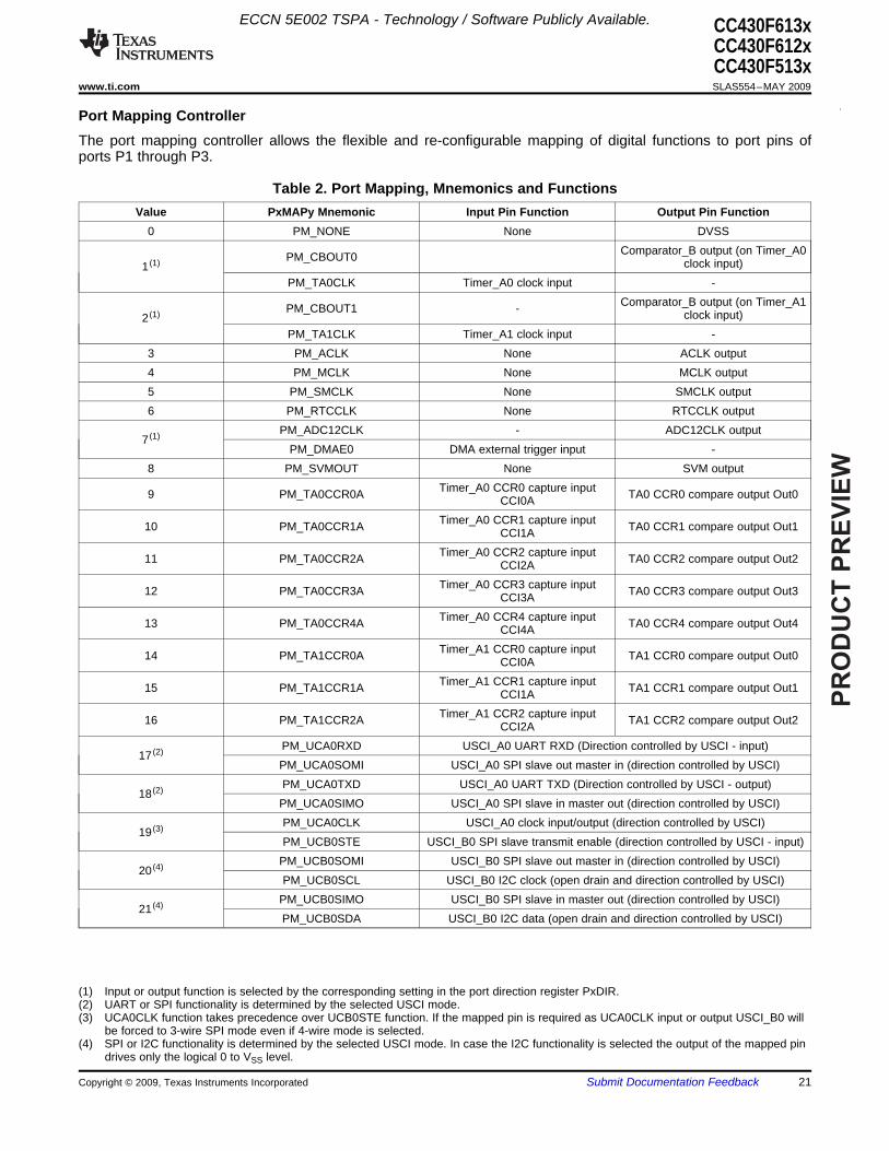
Port Mapping Controller
ECCN 5E002 TSPA - Technology / Software Publicly Available. CC430F613xCC430F612xCC430F513x
www.ti.com ........................................................................................................................................................................................................ SLAS554–MAY 2009
The port mapping controller allows the flexible and re-configurable mapping of digital functions to port pins ofports P1 through P3.
Table 2. Port Mapping, Mnemonics and FunctionsValue PxMAPy Mnemonic Input Pin Function Output Pin Function
0 PM_NONE None DVSSComparator_B output (on Timer_A0PM_CBOUT0 clock input)1 (1)
PM_TA0CLK Timer_A0 clock input -Comparator_B output (on Timer_A1PM_CBOUT1 - clock input)2 (1)
PM_TA1CLK Timer_A1 clock input -3 PM_ACLK None ACLK output4 PM_MCLK None MCLK output5 PM_SMCLK None SMCLK output6 PM_RTCCLK None RTCCLK output
PM_ADC12CLK - ADC12CLK output7 (1)
PM_DMAE0 DMA external trigger input -8 PM_SVMOUT None SVM output
Timer_A0 CCR0 capture input9 PM_TA0CCR0A TA0 CCR0 compare output Out0CCI0ATimer_A0 CCR1 capture input10 PM_TA0CCR1A TA0 CCR1 compare output Out1CCI1ATimer_A0 CCR2 capture input11 PM_TA0CCR2A TA0 CCR2 compare output Out2CCI2ATimer_A0 CCR3 capture input12 PM_TA0CCR3A TA0 CCR3 compare output Out3CCI3ATimer_A0 CCR4 capture input13 PM_TA0CCR4A TA0 CCR4 compare output Out4CCI4ATimer_A1 CCR0 capture input14 PM_TA1CCR0A TA1 CCR0 compare output Out0CCI0ATimer_A1 CCR1 capture input15 PM_TA1CCR1A TA1 CCR1 compare output Out1CCI1ATimer_A1 CCR2 capture input16 PM_TA1CCR2A TA1 CCR2 compare output Out2CCI2A
PM_UCA0RXD USCI_A0 UART RXD (Direction controlled by USCI - input)17 (2)
PM_UCA0SOMI USCI_A0 SPI slave out master in (direction controlled by USCI)PM_UCA0TXD USCI_A0 UART TXD (Direction controlled by USCI - output)
18 (2)PM_UCA0SIMO USCI_A0 SPI slave in master out (direction controlled by USCI)PM_UCA0CLK USCI_A0 clock input/output (direction controlled by USCI)
19 (3)PM_UCB0STE USCI_B0 SPI slave transmit enable (direction controlled by USCI - input)
PM_UCB0SOMI USCI_B0 SPI slave out master in (direction controlled by USCI)20 (4)
PM_UCB0SCL USCI_B0 I2C clock (open drain and direction controlled by USCI)PM_UCB0SIMO USCI_B0 SPI slave in master out (direction controlled by USCI)
21 (4)PM_UCB0SDA USCI_B0 I2C data (open drain and direction controlled by USCI)
(1) Input or output function is selected by the corresponding setting in the port direction register PxDIR.(2) UART or SPI functionality is determined by the selected USCI mode.(3) UCA0CLK function takes precedence over UCB0STE function. If the mapped pin is required as UCA0CLK input or output USCI_B0 will
be forced to 3-wire SPI mode even if 4-wire mode is selected.(4) SPI or I2C functionality is determined by the selected USCI mode. In case the I2C functionality is selected the output of the mapped pin
drives only the logical 0 to VSS level.
Copyright © 2009, Texas Instruments Incorporated Submit Documentation Feedback 21
PR
OD
UC
T P
RE
VIE
W
ECCN 5E002 TSPA - Technology / Software Publicly Available.CC430F613xCC430F612xCC430F513xSLAS554–MAY 2009 ........................................................................................................................................................................................................ www.ti.com
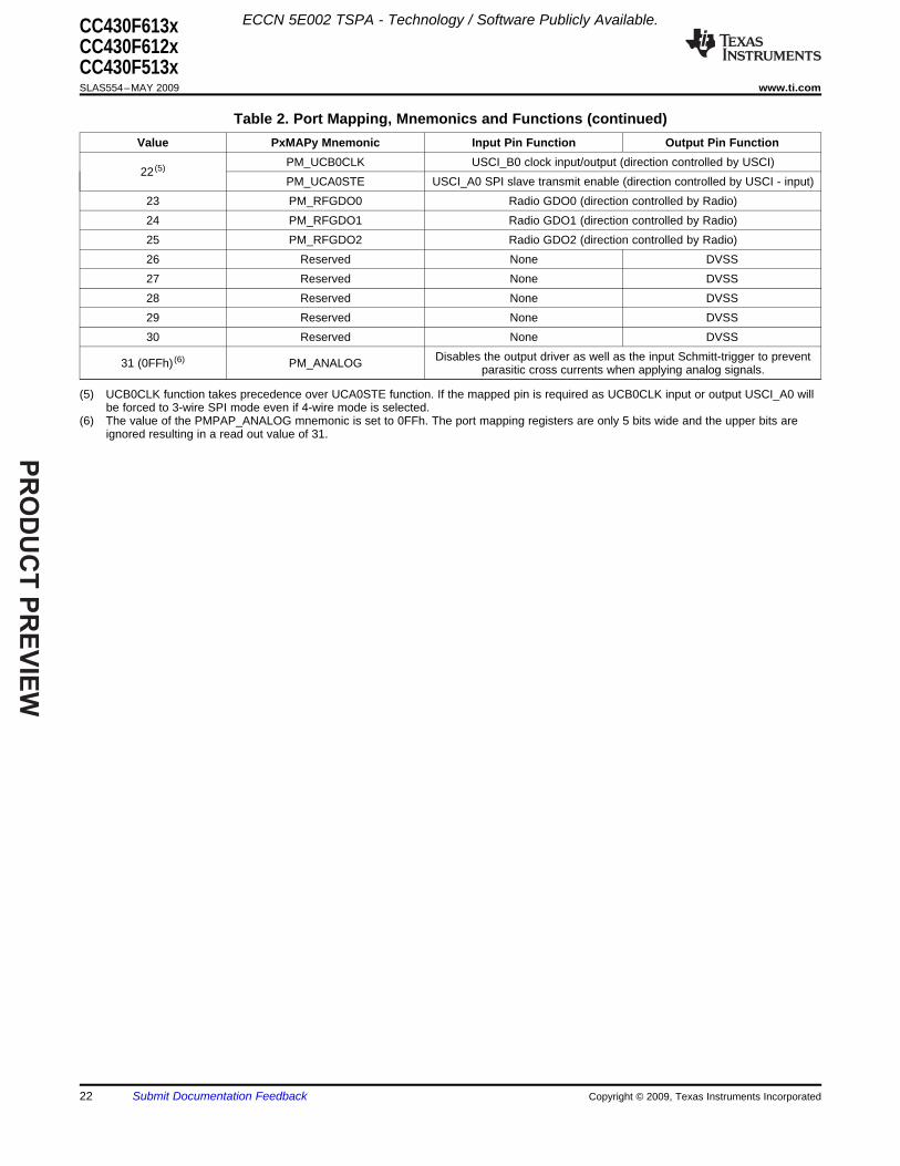
Table 2. Port Mapping, Mnemonics and Functions (continued)Value PxMAPy Mnemonic Input Pin Function Output Pin Function
PM_UCB0CLK USCI_B0 clock input/output (direction controlled by USCI)22 (5)
PM_UCA0STE USCI_A0 SPI slave transmit enable (direction controlled by USCI - input)23 PM_RFGDO0 Radio GDO0 (direction controlled by Radio)24 PM_RFGDO1 Radio GDO1 (direction controlled by Radio)25 PM_RFGDO2 Radio GDO2 (direction controlled by Radio)26 Reserved None DVSS27 Reserved None DVSS28 Reserved None DVSS29 Reserved None DVSS30 Reserved None DVSS
Disables the output driver as well as the input Schmitt-trigger to prevent31 (0FFh) (6) PM_ANALOG parasitic cross currents when applying analog signals.
(5) UCB0CLK function takes precedence over UCA0STE function. If the mapped pin is required as UCB0CLK input or output USCI_A0 willbe forced to 3-wire SPI mode even if 4-wire mode is selected.
(6) The value of the PMPAP_ANALOG mnemonic is set to 0FFh. The port mapping registers are only 5 bits wide and the upper bits areignored resulting in a read out value of 31.
22 Submit Documentation Feedback Copyright © 2009, Texas Instruments Incorporated
PR
OD
UC
T P
RE
VIE
W
ECCN 5E002 TSPA - Technology / Software Publicly Available. CC430F613xCC430F612xCC430F513x
www.ti.com ........................................................................................................................................................................................................ SLAS554–MAY 2009
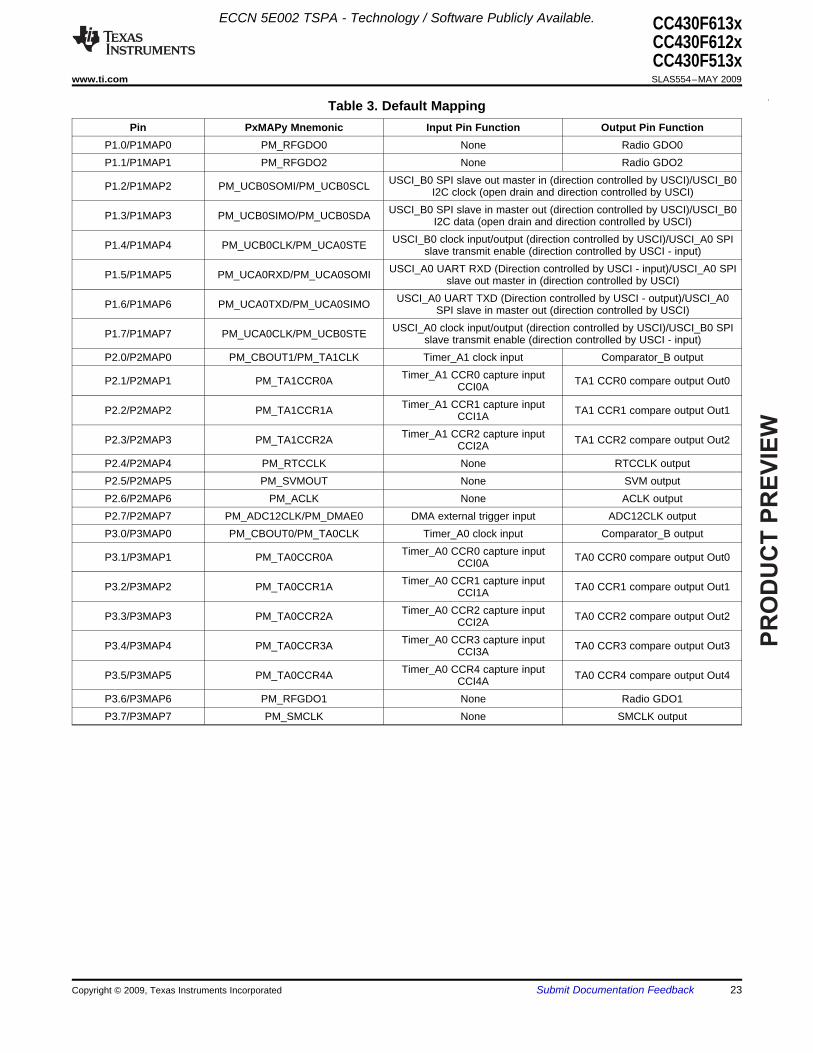
Table 3. Default MappingPin PxMAPy Mnemonic Input Pin Function Output Pin Function
P1.0/P1MAP0 PM_RFGDO0 None Radio GDO0P1.1/P1MAP1 PM_RFGDO2 None Radio GDO2
USCI_B0 SPI slave out master in (direction controlled by USCI)/USCI_B0P1.2/P1MAP2 PM_UCB0SOMI/PM_UCB0SCL I2C clock (open drain and direction controlled by USCI)USCI_B0 SPI slave in master out (direction controlled by USCI)/USCI_B0P1.3/P1MAP3 PM_UCB0SIMO/PM_UCB0SDA I2C data (open drain and direction controlled by USCI)USCI_B0 clock input/output (direction controlled by USCI)/USCI_A0 SPIP1.4/P1MAP4 PM_UCB0CLK/PM_UCA0STE slave transmit enable (direction controlled by USCI - input)
USCI_A0 UART RXD (Direction controlled by USCI - input)/USCI_A0 SPIP1.5/P1MAP5 PM_UCA0RXD/PM_UCA0SOMI slave out master in (direction controlled by USCI)USCI_A0 UART TXD (Direction controlled by USCI - output)/USCI_A0P1.6/P1MAP6 PM_UCA0TXD/PM_UCA0SIMO SPI slave in master out (direction controlled by USCI)
USCI_A0 clock input/output (direction controlled by USCI)/USCI_B0 SPIP1.7/P1MAP7 PM_UCA0CLK/PM_UCB0STE slave transmit enable (direction controlled by USCI - input)P2.0/P2MAP0 PM_CBOUT1/PM_TA1CLK Timer_A1 clock input Comparator_B output
Timer_A1 CCR0 capture inputP2.1/P2MAP1 PM_TA1CCR0A TA1 CCR0 compare output Out0CCI0ATimer_A1 CCR1 capture inputP2.2/P2MAP2 PM_TA1CCR1A TA1 CCR1 compare output Out1CCI1ATimer_A1 CCR2 capture inputP2.3/P2MAP3 PM_TA1CCR2A TA1 CCR2 compare output Out2CCI2A
P2.4/P2MAP4 PM_RTCCLK None RTCCLK outputP2.5/P2MAP5 PM_SVMOUT None SVM outputP2.6/P2MAP6 PM_ACLK None ACLK outputP2.7/P2MAP7 PM_ADC12CLK/PM_DMAE0 DMA external trigger input ADC12CLK outputP3.0/P3MAP0 PM_CBOUT0/PM_TA0CLK Timer_A0 clock input Comparator_B output
Timer_A0 CCR0 capture inputP3.1/P3MAP1 PM_TA0CCR0A TA0 CCR0 compare output Out0CCI0ATimer_A0 CCR1 capture inputP3.2/P3MAP2 PM_TA0CCR1A TA0 CCR1 compare output Out1CCI1ATimer_A0 CCR2 capture inputP3.3/P3MAP3 PM_TA0CCR2A TA0 CCR2 compare output Out2CCI2ATimer_A0 CCR3 capture inputP3.4/P3MAP4 PM_TA0CCR3A TA0 CCR3 compare output Out3CCI3ATimer_A0 CCR4 capture inputP3.5/P3MAP5 PM_TA0CCR4A TA0 CCR4 compare output Out4CCI4A
P3.6/P3MAP6 PM_RFGDO1 None Radio GDO1P3.7/P3MAP7 PM_SMCLK None SMCLK output
Copyright © 2009, Texas Instruments Incorporated Submit Documentation Feedback 23
PR
OD
UC
T P
RE
VIE
W
System Module (SYS)
Watchdog Timer (WDT_A)
ECCN 5E002 TSPA - Technology / Software Publicly Available.CC430F613xCC430F612xCC430F513xSLAS554–MAY 2009 ........................................................................................................................................................................................................ www.ti.com
The SYS module handles many of the system functions within the device. These include power on reset andpower up clear handling, NMI source selection and management, reset interrupt vector generators, boot straploader entry mechanisms, as well as, configuration management (device descriptors). It also includes a dataexchange mechanism via JTAG called a JTAG mailbox that can be used in the application.
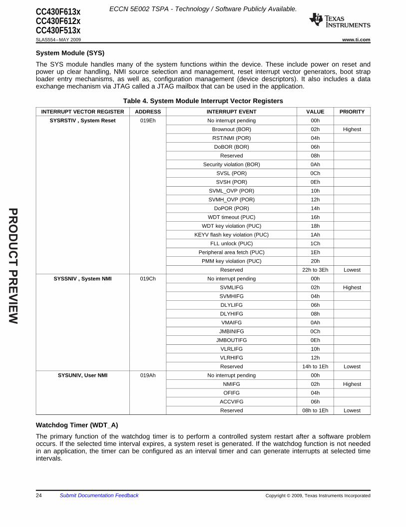
Table 4. System Module Interrupt Vector RegistersINTERRUPT VECTOR REGISTER ADDRESS INTERRUPT EVENT VALUE PRIORITY
SYSRSTIV , System Reset 019Eh No interrupt pending 00hBrownout (BOR) 02h HighestRST/NMI (POR) 04hDoBOR (BOR) 06h
Reserved 08hSecurity violation (BOR) 0Ah
SVSL (POR) 0ChSVSH (POR) 0Eh
SVML_OVP (POR) 10hSVMH_OVP (POR) 12h
DoPOR (POR) 14hWDT timeout (PUC) 16h
WDT key violation (PUC) 18hKEYV flash key violation (PUC) 1Ah
FLL unlock (PUC) 1ChPeripheral area fetch (PUC) 1Eh
PMM key violation (PUC) 20hReserved 22h to 3Eh Lowest
SYSSNIV , System NMI 019Ch No interrupt pending 00hSVMLIFG 02h HighestSVMHIFG 04hDLYLIFG 06hDLYHIFG 08hVMAIFG 0Ah
JMBINIFG 0ChJMBOUTIFG 0Eh
VLRLIFG 10hVLRHIFG 12hReserved 14h to 1Eh Lowest
SYSUNIV, User NMI 019Ah No interrupt pending 00hNMIFG 02h HighestOFIFG 04h
ACCVIFG 06hReserved 08h to 1Eh Lowest
The primary function of the watchdog timer is to perform a controlled system restart after a software problemoccurs. If the selected time interval expires, a system reset is generated. If the watchdog function is not neededin an application, the timer can be configured as an interval timer and can generate interrupts at selected timeintervals.
24 Submit Documentation Feedback Copyright © 2009, Texas Instruments Incorporated
PR
OD
UC
T P
RE
VIE
W
DMA Controller
ECCN 5E002 TSPA - Technology / Software Publicly Available. CC430F613xCC430F612xCC430F513x
www.ti.com ........................................................................................................................................................................................................ SLAS554–MAY 2009
The DMA controller allows movement of data from one memory address to another without CPU intervention.Using the DMA controller can increase the throughput of peripheral modules. The DMA controller reducessystem power consumption by allowing the CPU to remain in sleep mode, without having to awaken to movedata to or from a peripheral.
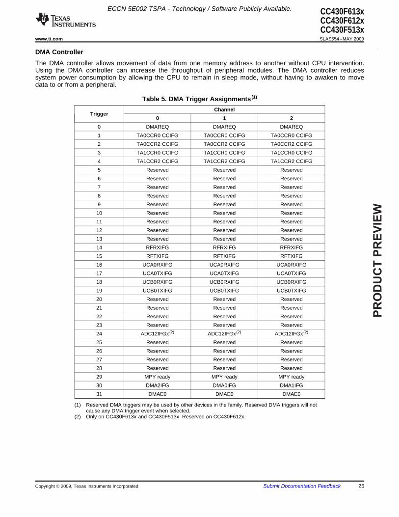
Table 5. DMA Trigger Assignments (1)
ChannelTrigger
0 1 20 DMAREQ DMAREQ DMAREQ1 TA0CCR0 CCIFG TA0CCR0 CCIFG TA0CCR0 CCIFG2 TA0CCR2 CCIFG TA0CCR2 CCIFG TA0CCR2 CCIFG3 TA1CCR0 CCIFG TA1CCR0 CCIFG TA1CCR0 CCIFG4 TA1CCR2 CCIFG TA1CCR2 CCIFG TA1CCR2 CCIFG5 Reserved Reserved Reserved6 Reserved Reserved Reserved7 Reserved Reserved Reserved8 Reserved Reserved Reserved9 Reserved Reserved Reserved10 Reserved Reserved Reserved11 Reserved Reserved Reserved12 Reserved Reserved Reserved13 Reserved Reserved Reserved14 RFRXIFG RFRXIFG RFRXIFG15 RFTXIFG RFTXIFG RFTXIFG16 UCA0RXIFG UCA0RXIFG UCA0RXIFG17 UCA0TXIFG UCA0TXIFG UCA0TXIFG18 UCB0RXIFG UCB0RXIFG UCB0RXIFG19 UCB0TXIFG UCB0TXIFG UCB0TXIFG20 Reserved Reserved Reserved21 Reserved Reserved Reserved22 Reserved Reserved Reserved23 Reserved Reserved Reserved24 ADC12IFGx (2) ADC12IFGx (2) ADC12IFGx (2)
25 Reserved Reserved Reserved26 Reserved Reserved Reserved27 Reserved Reserved Reserved28 Reserved Reserved Reserved29 MPY ready MPY ready MPY ready30 DMA2IFG DMA0IFG DMA1IFG31 DMAE0 DMAE0 DMAE0
(1) Reserved DMA triggers may be used by other devices in the family. Reserved DMA triggers will notcause any DMA trigger event when selected.
(2) Only on CC430F613x and CC430F513x. Reserved on CC430F612x.
Copyright © 2009, Texas Instruments Incorporated Submit Documentation Feedback 25
PR
OD
UC
T P
RE
VIE
W
CRC16
Hardware Multiplier
AES128 Accelerator
Universal Serial Communication Interface (USCI)
ECCN 5E002 TSPA - Technology / Software Publicly Available.CC430F613xCC430F612xCC430F513xSLAS554–MAY 2009 ........................................................................................................................................................................................................ www.ti.com
The CRC16 module produces a signature based on a sequence of entered data values and can be used for datachecking purposes. The CRC16 module signature is based on the CRC-CCITT standard.
The multiplication operation is supported by a dedicated peripheral module. The module performs operations with32-bit, 24-bit, 16-bit, and 8-bit operands. The module is capable of supporting signed and unsigned multiplicationas well as signed and unsigned multiply and accumulate operations.
The AES accelerator module performs en- and decryption of 128-bit data with 128-bit keys according to theAdvanced Encryption Standard (AES) (FIPS PUB 197) in hardware.
The USCI module is used for serial data communication. The USCI module supports synchronouscommunication protocols such as SPI (3 or 4 pin) and I2C, and asynchronous communication protocols such asUART, enhanced UART with automatic baudrate detection, and IrDA.
The USCI_An module provides support for SPI (3 or 4 pin), UART, enhanced UART, and IrDA.
The USCI_Bn module provides support for SPI (3 or 4 pin) and I2C.
A USCI_A0 and USCI_B0 module are implemented.
26 Submit Documentation Feedback Copyright © 2009, Texas Instruments Incorporated
PR
OD
UC
T P
RE
VIE
W
Timer0_A5
ECCN 5E002 TSPA - Technology / Software Publicly Available. CC430F613xCC430F612xCC430F513x
www.ti.com ........................................................................................................................................................................................................ SLAS554–MAY 2009
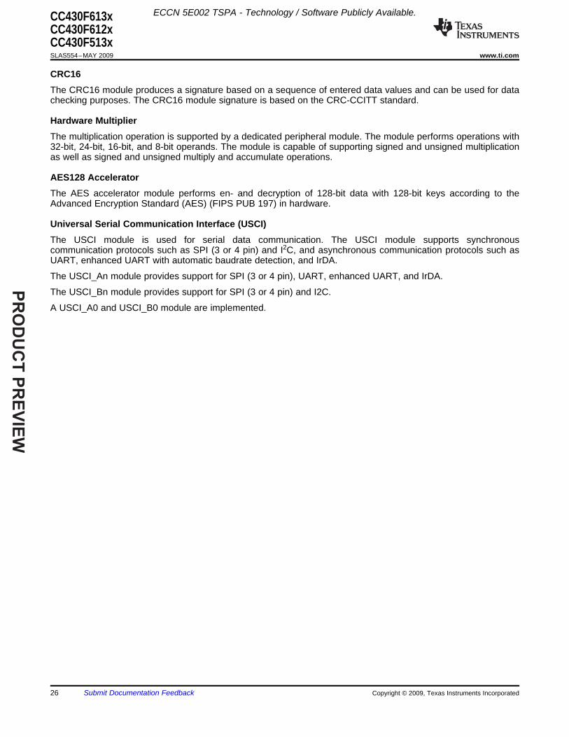
Timer0_A3 is a 16-bit timer/counter with three capture/compare registers. Timer0_A3 can support multiplecapture/compares, PWM outputs, and interval timing. Timer0_A3 also has extensive interrupt capabilities.Interrupts may be generated from the counter on overflow conditions and from each of the capture/compareregisters.
Table 6. Timer0_A5 Signal ConnectionsMODULE OUTPUT DEVICE OUTPUTDEVICE INPUT SIGNAL MODULE INPUT NAME MODULE BLOCK SIGNAL SIGNAL
PM_TA0CLK TACLKACLK (internal) ACLK
Timer NASMCLK (internal) SMCLK
RFCLK/192 (1) INCLKPM_TA0CCR0A CCI0A PM_TA0CCR0A
DVSS CCI0BCCR0 TA0
DVSS GNDDVCC VCC
PM_TA0CCR1A CCI1A PM_TA0CCR1AADC12 (internal) (2)
CBOUT (internal) CCI1B ADC12SHSx = {1}CCR1 TA1DVSS GNDDVCC VCC
PM_TA0CCR2A CCI2A PM_TA0CCR2AACLK (internal) CCI2B
CCR2 TA2DVSS GNDDVCC VCC
PM_TA0CCR3A CCI3A PM_TA0CCR3AGDO1 from Radio CCI3B(internal) CCR3 TA3
DVSS GNDDVCC VCC
PM_TA0CCR4A CCI4A PM_TA0CCR4AGDO2 from Radio CCI4B(internal) CCR4 TA4
DVSS GNDDVCC VCC
(1) If for a radio GDO output a different RFCLK divider setting is selected this divider setting will be also used for the Timer_A INCLK.(2) Only on CC430F613x and CC430F513x.
Copyright © 2009, Texas Instruments Incorporated Submit Documentation Feedback 27
PR
OD
UC
T P
RE
VIE
W
Timer1_A3
Real-Time Clock (RTC_A)
REF Voltage Reference
LCD_B (only CC430F613x and CC430F612x)
Comparator_B
ECCN 5E002 TSPA - Technology / Software Publicly Available.CC430F613xCC430F612xCC430F513xSLAS554–MAY 2009 ........................................................................................................................................................................................................ www.ti.com
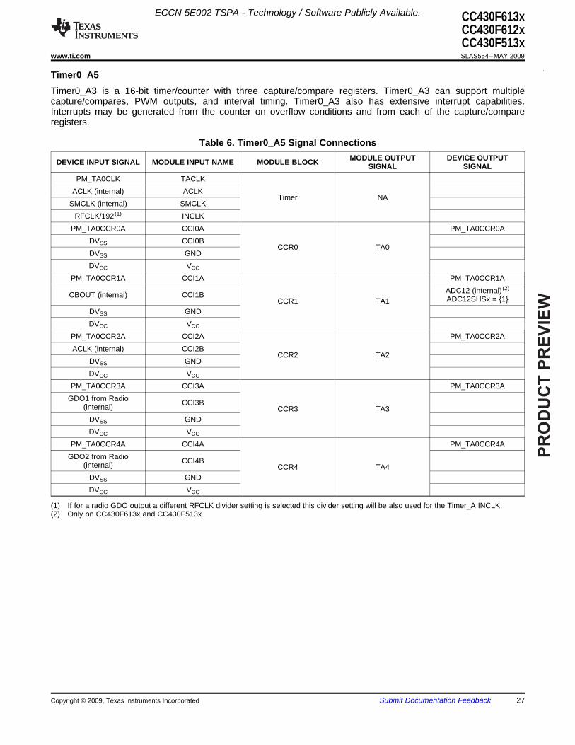
Timer1_A1 is a 16-bit timer/counter with one capture/compare registers. Timer1_A1 can support multiplecapture/compares, PWM outputs, and interval timing. Timer1_A1 also has extensive interrupt capabilities.Interrupts may be generated from the counter on overflow conditions and from each of the capture/compareregisters.
Table 7. Timer1_A3 Signal ConnectionsDEVICE OUTPUT
MODULE OUTPUT SIGNALDEVICE INPUT SIGNAL MODULE INPUT NAME MODULE BLOCK SIGNALPZ
PM_TA1CLK TACLKACLK (internal) ACLK
Timer NASMCLK (internal) SMCLK
RFCLK/192 (1) INCLKPM_TA1CCR0A CCI0A PM_TA1CCR0A
RF Async. Output CCI0B RF Async. Input (internal)(internal) CCR0 TA0DVSS GNDDVCC VCC
PM_TA1CCR1A CCI1A PM_TA1CCR1ACBOUT (internal) CCI1B
CCR1 TA1DVSS GNDDVCC VCC
PM_TA1CCR2A CCI2A PM_TA1CCR2AACLK (internal) CCI2B
CCR2 TA2DVSS GNDDVCC VCC
(1) If for a radio GDO output a different RFCLK divider setting is selected this divider setting will be also used for the Timer_A INCLK.
The RTC_A module can be used as a general-purpose 32-bit counter (counter mode) or as an integratedreal-time clock (RTC) (calendar mode). In counter mode, the RTC_A also includes two independent 8-bit timersthat can be cascaded to form a 16-bit timer/counter. Both timers can be read and written by software. Calendarmode integrates an internal calendar which compensates for months with less than 31 days and includes leapyear correction. The RTC_A also supports flexible alarm functions and offset-calibration hardware.
The reference module (REF) is responsible for generation of all critical reference voltages that can be used bythe various analog peripherals in the device. These include the ADC12_A, LCD_B, and COMP_B modules.
The LCD_B driver generates the segment and common signals required to drive a Liquid Crystal Display (LCD).The LCD_B controller has dedicated data memories to hold segment drive information. Common and segmentsignals are generated as defined by the mode. Static, 2-mux, 3-mux, and 4-mux LCDs are supported. Themodule can provide a LCD voltage independent of the supply voltage with its integrated charge pump. It ispossible to control the level of the LCD voltage and thus contrast by software. The module also provides anautomatic blinking capability for individual segments.
The primary function of the Comparator_B module is to support precision slope analog-to-digital conversions,battery voltage supervision, and monitoring of external analog signals.
28 Submit Documentation Feedback Copyright © 2009, Texas Instruments Incorporated
PR
OD
UC
T P
RE
VIE
W
ADC12_A (only CC430F613x and CC430F513x)
Embedded Emulation Module (EEM, S Version)
ECCN 5E002 TSPA - Technology / Software Publicly Available. CC430F613xCC430F612xCC430F513x
www.ti.com ........................................................................................................................................................................................................ SLAS554–MAY 2009
The ADC12_A module supports fast, 12-bit analog-to-digital conversions. The module implements a 12-bit SARcore, sample select control, reference generator and a 16 word conversion-and-control buffer. Theconversion-and-control buffer allows up to 16 independent ADC samples to be converted and stored without anyCPU intervention.
The Embedded Emulation Module (EEM) supports real-time in-system debugging. The S version of the EEMimplemented on all devices has the following features:• Three hardware triggers/breakpoints on memory access• One hardware trigger/breakpoint on CPU register write access• Up to four hardware triggers can be combined to form complex triggers/breakpoints• One cycle counter• Clock control on module level
Copyright © 2009, Texas Instruments Incorporated Submit Documentation Feedback 29
PR
OD
UC
T P
RE
VIE
W
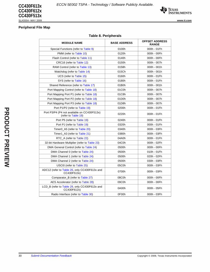
Peripheral File Map
ECCN 5E002 TSPA - Technology / Software Publicly Available.CC430F613xCC430F612xCC430F513xSLAS554–MAY 2009 ........................................................................................................................................................................................................ www.ti.com
Table 8. PeripheralsOFFSET ADDRESSMODULE NAME BASE ADDRESS RANGE
Special Functions (refer to Table 9) 0100h 000h - 01FhPMM (refer to Table 10) 0120h 000h - 00Fh
Flash Control (refer to Table 11) 0140h 000h - 00FhCRC16 (refer to Table 12) 0150h 000h - 007h
RAM Control (refer to Table 13) 0158h 000h - 001hWatchdog (refer to Table 14) 015Ch 000h - 001h
UCS (refer to Table 15) 0160h 000h - 01FhSYS (refer to Table 16) 0180h 000h - 01Fh
Shared Reference (refer to Table 17) 01B0h 000h - 001hPort Mapping Control (refer to Table 18) 01C0h 000h - 007hPort Mapping Port P1 (refer to Table 18) 01C8h 000h - 007hPort Mapping Port P2 (refer to Table 18) 01D0h 000h - 007hPort Mapping Port P3 (refer to Table 18) 01D8h 000h - 007h
Port P1/P2 (refer to Table 19) 0200h 000h - 01FhPort P3/P4 (P4 not available on CC430F513x) 0220h 000h - 01Fh(refer to Table 19)
Port P5 (refer to Table 19) 0240h 000h - 01FhPort PJ (refer to Table 19) 0320h 000h - 01Fh
Timer0_A5 (refer to Table 20) 0340h 000h - 03FhTimer1_A3 (refer to Table 21) 0380h 000h - 03Fh
RTC_A (refer to Table 22) 04A0h 000h - 01Fh32-bit Hardware Multiplier (refer to Table 23) 04C0h 000h - 02Fh
DMA General Control (refer to Table 24) 0500h 000h - 00FhDMA Channel 0 (refer to Table 24) 0500h 010h - 01FhDMA Channel 1 (refer to Table 24) 0500h 020h - 02FhDMA Channel 2 (refer to Table 24) 0500h 030h - 03Fh
USCI0 (refer to Table 25) 05C0h 000h - 03FhADC12 (refer to Table 26, only CC430F613x and 0700h 000h - 03FhCC430F513x)
Comparator_B (refer to Table 27) 08C0h 000h - 00FhAES Accelerator (refer to Table 28) 09C0h 000h - 00Fh
LCD_B (refer to Table 29, only CC430F613x and 0A00h 000h - 05FhCC430F612x)Radio Interface (refer to Table 30) 0F00h 000h - 03Fh
30 Submit Documentation Feedback Copyright © 2009, Texas Instruments Incorporated
PR
OD
UC
T P
RE
VIE
W
ECCN 5E002 TSPA - Technology / Software Publicly Available. CC430F613xCC430F612xCC430F513x
www.ti.com ........................................................................................................................................................................................................ SLAS554–MAY 2009
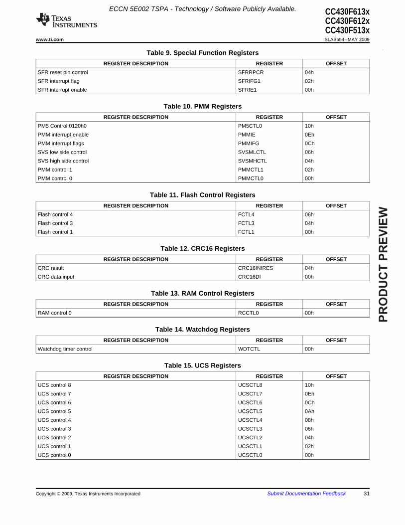
Table 9. Special Function RegistersREGISTER DESCRIPTION REGISTER OFFSET
SFR reset pin control SFRRPCR 04hSFR interrupt flag SFRIFG1 02hSFR interrupt enable SFRIE1 00h
Table 10. PMM RegistersREGISTER DESCRIPTION REGISTER OFFSET
PM5 Control 0120h0 PM5CTL0 10hPMM interrupt enable PMMIE 0EhPMM interrupt flags PMMIFG 0ChSVS low side control SVSMLCTL 06hSVS high side control SVSMHCTL 04hPMM control 1 PMMCTL1 02hPMM control 0 PMMCTL0 00h
Table 11. Flash Control RegistersREGISTER DESCRIPTION REGISTER OFFSET
Flash control 4 FCTL4 06hFlash control 3 FCTL3 04hFlash control 1 FCTL1 00h
Table 12. CRC16 RegistersREGISTER DESCRIPTION REGISTER OFFSET
CRC result CRC16INIRES 04hCRC data input CRC16DI 00h
Table 13. RAM Control RegistersREGISTER DESCRIPTION REGISTER OFFSET
RAM control 0 RCCTL0 00h
Table 14. Watchdog RegistersREGISTER DESCRIPTION REGISTER OFFSET
Watchdog timer control WDTCTL 00h
Table 15. UCS RegistersREGISTER DESCRIPTION REGISTER OFFSET
UCS control 8 UCSCTL8 10hUCS control 7 UCSCTL7 0EhUCS control 6 UCSCTL6 0ChUCS control 5 UCSCTL5 0AhUCS control 4 UCSCTL4 08hUCS control 3 UCSCTL3 06hUCS control 2 UCSCTL2 04hUCS control 1 UCSCTL1 02hUCS control 0 UCSCTL0 00h
Copyright © 2009, Texas Instruments Incorporated Submit Documentation Feedback 31

PR
OD
UC
T P
RE
VIE
W
ECCN 5E002 TSPA - Technology / Software Publicly Available.CC430F613xCC430F612xCC430F513xSLAS554–MAY 2009 ........................................................................................................................................................................................................ www.ti.com
Table 16. SYS RegistersREGISTER DESCRIPTION REGISTER OFFSET
Reset vector generator SYSRSTIV 1EhSystem NMI vector generator SYSSNIV 1ChUser NMI vector generator SYSUNIV 1AhBus Error vector generator SYSBERRIV 18hJTAG mailbox output 1 SYSJMBO1 0EhJTAG mailbox output 0 SYSJMBO0 0ChJTAG mailbox input 1 SYSJMBI1 0AhJTAG mailbox input 0 SYSJMBI0 08hJTAG mailbox control SYSJMBC 06hBootstrap loader configuration area SYSBSLC 02hSystem control SYSCTL 00h
Table 17. Shared Reference RegistersREGISTER DESCRIPTION REGISTER OFFSET
Shared reference control REFCTL 00h
Table 18. Port Mapping RegistersREGISTER DESCRIPTION REGISTER OFFSET
Port mapping password register PMAPPWD 00hPort mapping control register PMAPCTL 02hPort P1.0 mapping register P1MAP0 00hPort P1.1 mapping register P1MAP1 01hPort P1.2 mapping register P1MAP2 02hPort P1.3 mapping register P1MAP3 03hPort P1.4 mapping register P1MAP4 04hPort P1.5 mapping register P1MAP5 05hPort P1.6 mapping register P1MAP6 06hPort P1.7 mapping register P1MAP7 07hPort P2.0 mapping register P2MAP0 00hPort P2.1 mapping register P2MAP2 01hPort P2.2 mapping register P2MAP2 02hPort P2.3 mapping register P2MAP3 03hPort P2.4 mapping register P2MAP4 04hPort P2.5 mapping register P2MAP5 05hPort P2.6 mapping register P2MAP6 06hPort P2.7 mapping register P2MAP7 07hPort P3.0 mapping register P3MAP0 00hPort P3.1 mapping register P3MAP3 01hPort P3.2 mapping register P3MAP2 02hPort P3.3 mapping register P3MAP3 03hPort P3.4 mapping register P3MAP4 04hPort P3.5 mapping register P3MAP5 05hPort P3.6 mapping register P3MAP6 06hPort P3.7 mapping register P3MAP7 07h
32 Submit Documentation Feedback Copyright © 2009, Texas Instruments Incorporated
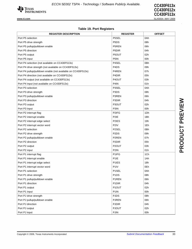
PR
OD
UC
T P
RE
VIE
W
ECCN 5E002 TSPA - Technology / Software Publicly Available. CC430F613xCC430F612xCC430F513x
www.ti.com ........................................................................................................................................................................................................ SLAS554–MAY 2009
Table 19. Port RegistersREGISTER DESCRIPTION REGISTER OFFSET
Port P5 selection P5SEL 0AhPort P5 drive strength P5DS 08hPort P5 pullup/pulldown enable P5REN 06hPort P5 direction P5DIR 04hPort P5 output P5OUT 02hPort P5 input P5IN 00hPort P4 selection (not available on CC430F513x) P4SEL 0BhPort P4 drive strength (not available on CC430F513x) P4DS 09hPort P4 pullup/pulldown enable (not available on CC430F513x) P4REN 07hPort P4 direction (not available on CC430F513x) P4DIR 05hPort P4 output (not available on CC430F513x) P4OUT 03hPort P4 input (not available on CC430F513x) P4IN 01hPort P3 selection P3SEL 0AhPort P3 drive strength P3DS 08hPort P3 pullup/pulldown enable P3REN 06hPort P3 direction P3DIR 04hPort P3 output P3OUT 02hPort P3 input P3IN 00hPort P2 interrupt flag P2IFG 1DhPort P2 interrupt enable P2IE 1BhPort P2 interrupt edge select P2IES 19hPort P2 interrupt vector word P2IV 1EhPort P2 selection P2SEL 0BhPort P2 drive strength P2DS 09hPort P2 pullup/pulldown enable P2REN 07hPort P2 direction P2DIR 05hPort P2 output P2OUT 03hPort P2 input P2IN 01hPort P1 interrupt flag P1IFG 1ChPort P1 interrupt enable P1IE 1AhPort P1 interrupt edge select P1IES 18hPort P1 interrupt vector word P1IV 0EhPort P1 selection P1SEL 0AhPort P1 drive strength P1DS 08hPort P1 pullup/pulldown enable P1REN 06hPort P1 direction P1DIR 04hPort P1 output P1OUT 02hPort P1 input P1IN 00hPort PJ drive strength PJDS 08hPort PJ pullup/pulldown enable PJREN 06hPort PJ direction PJDIR 04hPort PJ output PJOUT 02hPort PJ input PJIN 00h
Copyright © 2009, Texas Instruments Incorporated Submit Documentation Feedback 33
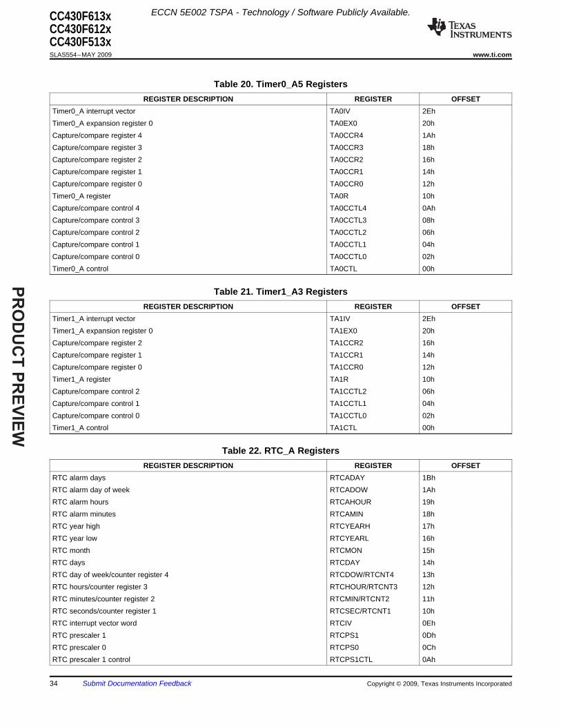
PR
OD
UC
T P
RE
VIE
W
ECCN 5E002 TSPA - Technology / Software Publicly Available.CC430F613xCC430F612xCC430F513xSLAS554–MAY 2009 ........................................................................................................................................................................................................ www.ti.com
Table 20. Timer0_A5 RegistersREGISTER DESCRIPTION REGISTER OFFSET
Timer0_A interrupt vector TA0IV 2EhTimer0_A expansion register 0 TA0EX0 20hCapture/compare register 4 TA0CCR4 1AhCapture/compare register 3 TA0CCR3 18hCapture/compare register 2 TA0CCR2 16hCapture/compare register 1 TA0CCR1 14hCapture/compare register 0 TA0CCR0 12hTimer0_A register TA0R 10hCapture/compare control 4 TA0CCTL4 0AhCapture/compare control 3 TA0CCTL3 08hCapture/compare control 2 TA0CCTL2 06hCapture/compare control 1 TA0CCTL1 04hCapture/compare control 0 TA0CCTL0 02hTimer0_A control TA0CTL 00h
Table 21. Timer1_A3 RegistersREGISTER DESCRIPTION REGISTER OFFSET
Timer1_A interrupt vector TA1IV 2EhTimer1_A expansion register 0 TA1EX0 20hCapture/compare register 2 TA1CCR2 16hCapture/compare register 1 TA1CCR1 14hCapture/compare register 0 TA1CCR0 12hTimer1_A register TA1R 10hCapture/compare control 2 TA1CCTL2 06hCapture/compare control 1 TA1CCTL1 04hCapture/compare control 0 TA1CCTL0 02hTimer1_A control TA1CTL 00h
Table 22. RTC_A RegistersREGISTER DESCRIPTION REGISTER OFFSET
RTC alarm days RTCADAY 1BhRTC alarm day of week RTCADOW 1AhRTC alarm hours RTCAHOUR 19hRTC alarm minutes RTCAMIN 18hRTC year high RTCYEARH 17hRTC year low RTCYEARL 16hRTC month RTCMON 15hRTC days RTCDAY 14hRTC day of week/counter register 4 RTCDOW/RTCNT4 13hRTC hours/counter register 3 RTCHOUR/RTCNT3 12hRTC minutes/counter register 2 RTCMIN/RTCNT2 11hRTC seconds/counter register 1 RTCSEC/RTCNT1 10hRTC interrupt vector word RTCIV 0EhRTC prescaler 1 RTCPS1 0DhRTC prescaler 0 RTCPS0 0ChRTC prescaler 1 control RTCPS1CTL 0Ah
34 Submit Documentation Feedback Copyright © 2009, Texas Instruments Incorporated
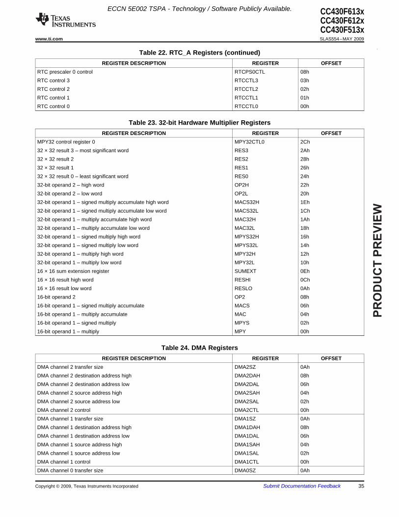
PR
OD
UC
T P
RE
VIE
W
ECCN 5E002 TSPA - Technology / Software Publicly Available. CC430F613xCC430F612xCC430F513x
www.ti.com ........................................................................................................................................................................................................ SLAS554–MAY 2009
Table 22. RTC_A Registers (continued)REGISTER DESCRIPTION REGISTER OFFSET
RTC prescaler 0 control RTCPS0CTL 08hRTC control 3 RTCCTL3 03hRTC control 2 RTCCTL2 02hRTC control 1 RTCCTL1 01hRTC control 0 RTCCTL0 00h
Table 23. 32-bit Hardware Multiplier RegistersREGISTER DESCRIPTION REGISTER OFFSET
MPY32 control register 0 MPY32CTL0 2Ch32 × 32 result 3 – most significant word RES3 2Ah32 × 32 result 2 RES2 28h32 × 32 result 1 RES1 26h32 × 32 result 0 – least significant word RES0 24h32-bit operand 2 – high word OP2H 22h32-bit operand 2 – low word OP2L 20h32-bit operand 1 – signed multiply accumulate high word MACS32H 1Eh32-bit operand 1 – signed multiply accumulate low word MACS32L 1Ch32-bit operand 1 – multiply accumulate high word MAC32H 1Ah32-bit operand 1 – multiply accumulate low word MAC32L 18h32-bit operand 1 – signed multiply high word MPYS32H 16h32-bit operand 1 – signed multiply low word MPYS32L 14h32-bit operand 1 – multiply high word MPY32H 12h32-bit operand 1 – multiply low word MPY32L 10h16 × 16 sum extension register SUMEXT 0Eh16 × 16 result high word RESHI 0Ch16 × 16 result low word RESLO 0Ah16-bit operand 2 OP2 08h16-bit operand 1 – signed multiply accumulate MACS 06h16-bit operand 1 – multiply accumulate MAC 04h16-bit operand 1 – signed multiply MPYS 02h16-bit operand 1 – multiply MPY 00h
Table 24. DMA RegistersREGISTER DESCRIPTION REGISTER OFFSET
DMA channel 2 transfer size DMA2SZ 0AhDMA channel 2 destination address high DMA2DAH 08hDMA channel 2 destination address low DMA2DAL 06hDMA channel 2 source address high DMA2SAH 04hDMA channel 2 source address low DMA2SAL 02hDMA channel 2 control DMA2CTL 00hDMA channel 1 transfer size DMA1SZ 0AhDMA channel 1 destination address high DMA1DAH 08hDMA channel 1 destination address low DMA1DAL 06hDMA channel 1 source address high DMA1SAH 04hDMA channel 1 source address low DMA1SAL 02hDMA channel 1 control DMA1CTL 00hDMA channel 0 transfer size DMA0SZ 0Ah
Copyright © 2009, Texas Instruments Incorporated Submit Documentation Feedback 35
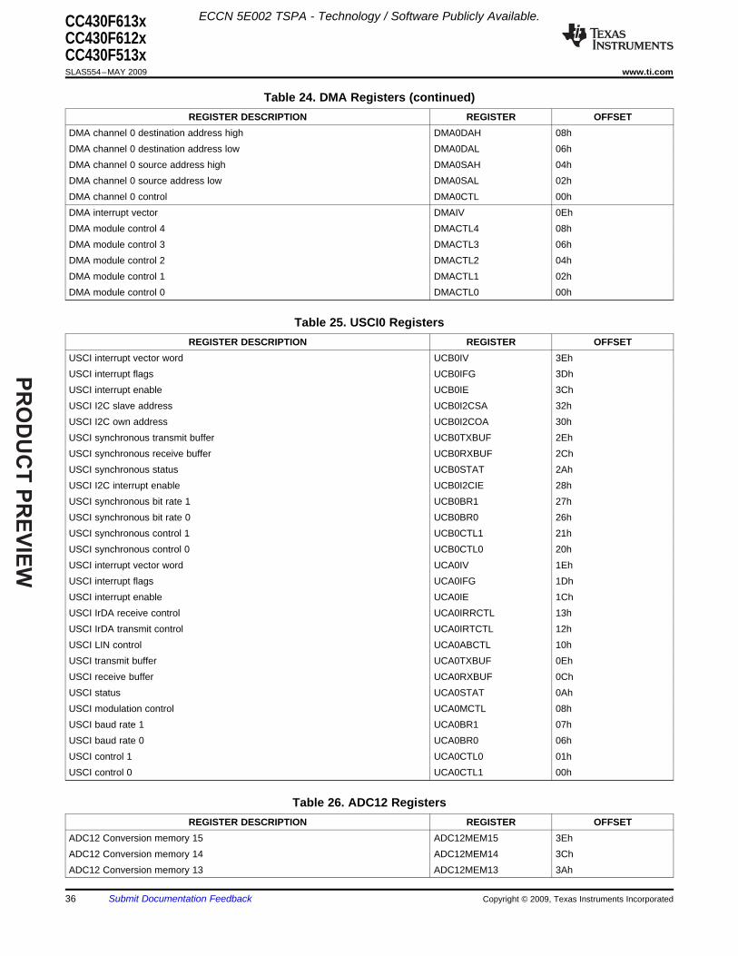
PR
OD
UC
T P
RE
VIE
W
ECCN 5E002 TSPA - Technology / Software Publicly Available.CC430F613xCC430F612xCC430F513xSLAS554–MAY 2009 ........................................................................................................................................................................................................ www.ti.com
Table 24. DMA Registers (continued)REGISTER DESCRIPTION REGISTER OFFSET
DMA channel 0 destination address high DMA0DAH 08hDMA channel 0 destination address low DMA0DAL 06hDMA channel 0 source address high DMA0SAH 04hDMA channel 0 source address low DMA0SAL 02hDMA channel 0 control DMA0CTL 00hDMA interrupt vector DMAIV 0EhDMA module control 4 DMACTL4 08hDMA module control 3 DMACTL3 06hDMA module control 2 DMACTL2 04hDMA module control 1 DMACTL1 02hDMA module control 0 DMACTL0 00h
Table 25. USCI0 RegistersREGISTER DESCRIPTION REGISTER OFFSET
USCI interrupt vector word UCB0IV 3EhUSCI interrupt flags UCB0IFG 3DhUSCI interrupt enable UCB0IE 3ChUSCI I2C slave address UCB0I2CSA 32hUSCI I2C own address UCB0I2COA 30hUSCI synchronous transmit buffer UCB0TXBUF 2EhUSCI synchronous receive buffer UCB0RXBUF 2ChUSCI synchronous status UCB0STAT 2AhUSCI I2C interrupt enable UCB0I2CIE 28hUSCI synchronous bit rate 1 UCB0BR1 27hUSCI synchronous bit rate 0 UCB0BR0 26hUSCI synchronous control 1 UCB0CTL1 21hUSCI synchronous control 0 UCB0CTL0 20hUSCI interrupt vector word UCA0IV 1EhUSCI interrupt flags UCA0IFG 1DhUSCI interrupt enable UCA0IE 1ChUSCI IrDA receive control UCA0IRRCTL 13hUSCI IrDA transmit control UCA0IRTCTL 12hUSCI LIN control UCA0ABCTL 10hUSCI transmit buffer UCA0TXBUF 0EhUSCI receive buffer UCA0RXBUF 0ChUSCI status UCA0STAT 0AhUSCI modulation control UCA0MCTL 08hUSCI baud rate 1 UCA0BR1 07hUSCI baud rate 0 UCA0BR0 06hUSCI control 1 UCA0CTL0 01hUSCI control 0 UCA0CTL1 00h
Table 26. ADC12 RegistersREGISTER DESCRIPTION REGISTER OFFSET
ADC12 Conversion memory 15 ADC12MEM15 3EhADC12 Conversion memory 14 ADC12MEM14 3ChADC12 Conversion memory 13 ADC12MEM13 3Ah
36 Submit Documentation Feedback Copyright © 2009, Texas Instruments Incorporated
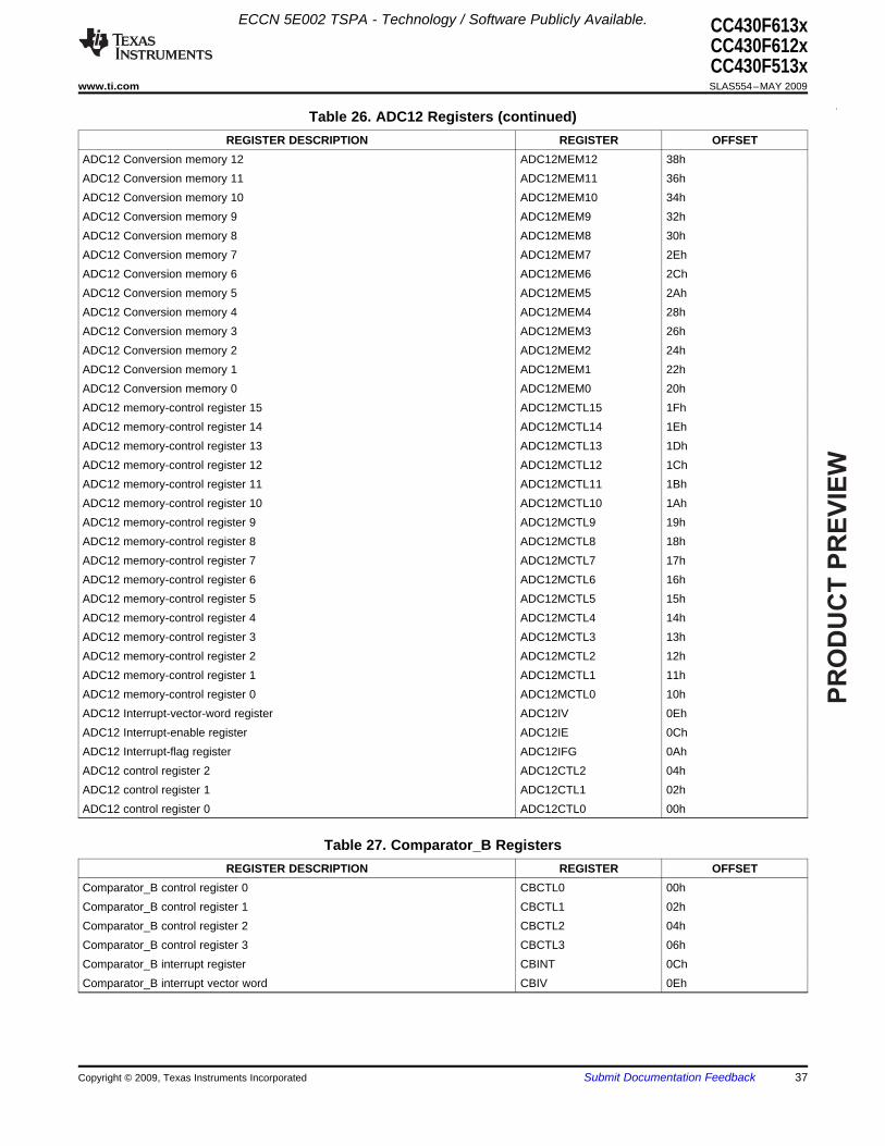
PR
OD
UC
T P
RE
VIE
W
ECCN 5E002 TSPA - Technology / Software Publicly Available. CC430F613xCC430F612xCC430F513x
www.ti.com ........................................................................................................................................................................................................ SLAS554–MAY 2009
Table 26. ADC12 Registers (continued)REGISTER DESCRIPTION REGISTER OFFSET
ADC12 Conversion memory 12 ADC12MEM12 38hADC12 Conversion memory 11 ADC12MEM11 36hADC12 Conversion memory 10 ADC12MEM10 34hADC12 Conversion memory 9 ADC12MEM9 32hADC12 Conversion memory 8 ADC12MEM8 30hADC12 Conversion memory 7 ADC12MEM7 2EhADC12 Conversion memory 6 ADC12MEM6 2ChADC12 Conversion memory 5 ADC12MEM5 2AhADC12 Conversion memory 4 ADC12MEM4 28hADC12 Conversion memory 3 ADC12MEM3 26hADC12 Conversion memory 2 ADC12MEM2 24hADC12 Conversion memory 1 ADC12MEM1 22hADC12 Conversion memory 0 ADC12MEM0 20hADC12 memory-control register 15 ADC12MCTL15 1FhADC12 memory-control register 14 ADC12MCTL14 1EhADC12 memory-control register 13 ADC12MCTL13 1DhADC12 memory-control register 12 ADC12MCTL12 1ChADC12 memory-control register 11 ADC12MCTL11 1BhADC12 memory-control register 10 ADC12MCTL10 1AhADC12 memory-control register 9 ADC12MCTL9 19hADC12 memory-control register 8 ADC12MCTL8 18hADC12 memory-control register 7 ADC12MCTL7 17hADC12 memory-control register 6 ADC12MCTL6 16hADC12 memory-control register 5 ADC12MCTL5 15hADC12 memory-control register 4 ADC12MCTL4 14hADC12 memory-control register 3 ADC12MCTL3 13hADC12 memory-control register 2 ADC12MCTL2 12hADC12 memory-control register 1 ADC12MCTL1 11hADC12 memory-control register 0 ADC12MCTL0 10hADC12 Interrupt-vector-word register ADC12IV 0EhADC12 Interrupt-enable register ADC12IE 0ChADC12 Interrupt-flag register ADC12IFG 0AhADC12 control register 2 ADC12CTL2 04hADC12 control register 1 ADC12CTL1 02hADC12 control register 0 ADC12CTL0 00h
Table 27. Comparator_B RegistersREGISTER DESCRIPTION REGISTER OFFSET
Comparator_B control register 0 CBCTL0 00hComparator_B control register 1 CBCTL1 02hComparator_B control register 2 CBCTL2 04hComparator_B control register 3 CBCTL3 06hComparator_B interrupt register CBINT 0ChComparator_B interrupt vector word CBIV 0Eh
Copyright © 2009, Texas Instruments Incorporated Submit Documentation Feedback 37
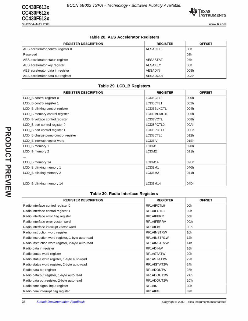
PR
OD
UC
T P
RE
VIE
W
ECCN 5E002 TSPA - Technology / Software Publicly Available.CC430F613xCC430F612xCC430F513xSLAS554–MAY 2009 ........................................................................................................................................................................................................ www.ti.com
Table 28. AES Accelerator RegistersREGISTER DESCRIPTION REGISTER OFFSET
AES accelerator control register 0 AESACTL0 00hReserved 02hAES accelerator status register AESASTAT 04hAES accelerator key register AESAKEY 06hAES accelerator data in register AESADIN 008hAES accelerator data out register AESADOUT 00Ah
Table 29. LCD_B RegistersREGISTER DESCRIPTION REGISTER OFFSET
LCD_B control register 0 LCDBCTL0 000hLCD_B control register 1 LCDBCTL1 002hLCD_B blinking control register LCDBBLKCTL 004hLCD_B memory control register LCDBMEMCTL 006hLCD_B voltage control register LCDBVCTL 008hLCD_B port control register 0 LCDBPCTL0 00AhLCD_B port control register 1 LCDBPCTL1 00ChLCD_B charge pump control register LCDBCTL0 012hLCD_B interrupt vector word LCDBIV 01EhLCD_B memory 1 LCDM1 020hLCD_B memory 2 LCDM2 021h...LCD_B memory 14 LCDM14 02DhLCD_B blinking memory 1 LCDBM1 040hLCD_B blinking memory 2 LCDBM2 041h...LCD_B blinking memory 14 LCDBM14 04Dh
Table 30. Radio Interface RegistersREGISTER DESCRIPTION REGISTER OFFSET
Radio interface control register 0 RF1AIFCTL0 00hRadio interface control register 1 RF1AIFCTL1 02hRadio interface error flag register RF1AIFERR 06hRadio interface error vector word RF1AIFERRV 0ChRadio interface interrupt vector word RF1AIFIV 0EhRadio instruction word register RF1AINSTRW 10hRadio instruction word register, 1-byte auto-read RF1AINSTR1W 12hRadio instruction word register, 2-byte auto-read RF1AINSTR2W 14hRadio data in register RF1ADINW 16hRadio status word register RF1ASTATW 20hRadio status word register, 1-byte auto-read RF1ASTAT1W 22hRadio status word register, 2-byte auto-read RF1AISTAT2W 24hRadio data out register RF1ADOUTW 28hRadio data out register, 1-byte auto-read RF1ADOUT1W 2AhRadio data out register, 2-byte auto-read RF1ADOUT2W 2ChRadio core signal input register RF1AIN 30hRadio core interrupt flag register RF1AIFG 32h
38 Submit Documentation Feedback Copyright © 2009, Texas Instruments Incorporated
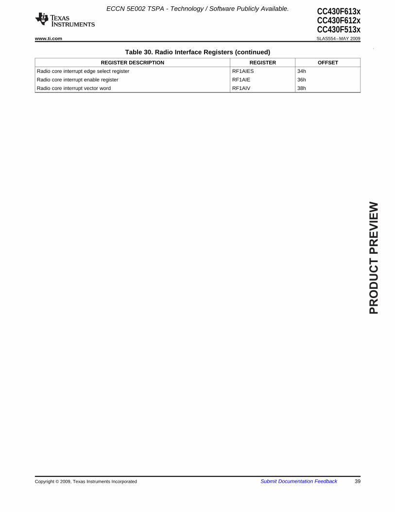
PR
OD
UC
T P
RE
VIE
W
ECCN 5E002 TSPA - Technology / Software Publicly Available. CC430F613xCC430F612xCC430F513x
www.ti.com ........................................................................................................................................................................................................ SLAS554–MAY 2009
Table 30. Radio Interface Registers (continued)REGISTER DESCRIPTION REGISTER OFFSET
Radio core interrupt edge select register RF1AIES 34hRadio core interrupt enable register RF1AIE 36hRadio core interrupt vector word RF1AIV 38h
Copyright © 2009, Texas Instruments Incorporated Submit Documentation Feedback 39

PR
OD
UC
T P
RE
VIE
W
Absolute Maximum Ratings (1)
Recommended Operating Conditions
ECCN 5E002 TSPA - Technology / Software Publicly Available.CC430F613xCC430F612xCC430F513xSLAS554–MAY 2009 ........................................................................................................................................................................................................ www.ti.com
over operating free-air temperature range (unless otherwise noted)
Voltage applied at VCC to VSS –0.3 V to 4.1 VVoltage applied to any pin (except RF_P, RF_N, and R_BIAS) (2) –0.3 V to VCC + 0.3 V, max. 4.1VVoltage applied to RF_P, RF_N, and R_BIAS (2) –0.3 V to 2.0 VInput RF level at pins RF_P and RF_N 10dBmDiode current at any device terminal ±2 mA
Unprogrammed device (3) –55°C to 150°CStorage temperature range, Tstg Programmed device (3) –40°C to 105°C
(1) Stresses beyond those listed under "absolute maximum ratings" may cause permanent damage to the device. These are stress ratingsonly, and functional operation of the device at these or any other conditions beyond those indicated under "recommended operatingconditions" is not implied. Exposure to absolute-maximum-rated conditions for extended periods may affect device reliability.
(2) All voltages referenced to VSS.(3) Higher temperature may be applied during board soldering according to the current JEDEC J-STD-020 specification with peak reflow
temperatures not higher than classified on the device label on the shipping boxes or reels.
MIN NOM MAX UNITPMMCOREVx = 0 (defaultSupply voltage range during program execution and flash 1.8 3.6 Vafter POR)VCC programming (VCC = AVCC = DVCC) (1) with PMM default
settings. Radio is not operational with PMMCOREVx = 0, 1. PMMCOREVx = 1 2.0 3.6 VSupply voltage range during program execution, flash
VCC programming and radio operation (VCC = AVCC = DVCC)(1) PMMCOREVx = 2 2.2 3.6 Vwith PMM default settings.Supply voltage range during program execution, flashprogramming and radio operation (VCC = AVCC = DVCC)(1) PMMCOREVx = 2,
VCC with PMMCOREVx = 2, high-side SVS level lowered SVSHRVLx=SVSHRRRLx=1 2.0 3.6 V(SVSHRVLx=SVSHRRRLx=1) or high-side SVS disabled or SVSHE=0(SVSHE=0). (2)
VSS Supply voltage (VSS = AVSS = DVSS) 0 VTA Operating free-air temperature –40 85 °CCVCORE Capacitor at VCORE 470 nF
PMMCOREVx = 0, 1MCLK sourced by any clock 0 12.0 MHzsource.PMMCOREVx = 2
fSYSTEM Processor (MCLK) frequency (3) MCLK sourced by any clock 0 25.0 MHzsource.PMMCOREVx = 2MCLK sourced by RF crystal 0 27.0 MHzoscillator or FLL.
(1) It is recommended to power AVCC and DVCC from the same source. A maximum difference of 0.3 V between AVCC and DVCC can betolerated during power up and operation.
(2) Lowering the high-side SVS level or disabling the high-side SVS might cause the LDO to operate out of regulation but the core voltagewill still stay within it's limits and is still supervised by the low-side SVS ensuring reliable operation.
(3) Modules may have a different maximum input clock specification. Refer to the specification of the respective module in this data sheet.
40 Submit Documentation Feedback Copyright © 2009, Texas Instruments Incorporated
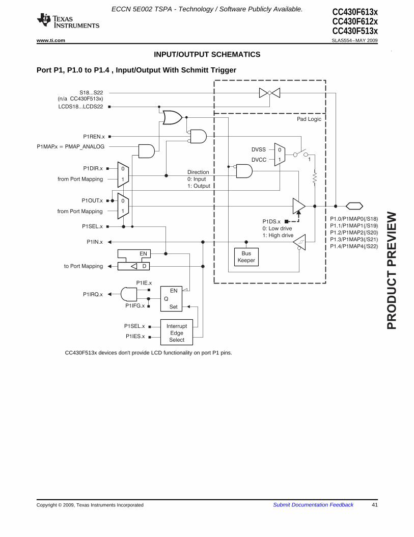
PR
OD
UC
T P
RE
VIE
W
INPUT/OUTPUT SCHEMATICS
Port P1, P1.0 to P1.4 , Input/Output With Schmitt Trigger
P1.0/P1MAP0(/S18)
P1.1/P1MAP1(/S19)
P1.2/P1MAP2(/S20)
P1.3/P1MAP3(/S21)
P1.4/P1MAP4(/S22)
Direction
0: Input
1: Output
P1SEL.x
1
0P1DIR.x
P1IN.x
P1IRQ.x
EN
to Port Mapping
1
0
from Port Mapping
P1OUT.x
Interrupt
Select
Edge
Q
EN
Set
P1 .SEL x
P1IES x.
P1IFG.x
P1IE.x
1
0DVSS
DVCC 1
P1DS.x
0: Low drive
1: High drive
D
from Port Mapping
S18...S22
LCDS18...LCDS22
Pad Logic
P1REN.x
P1MAP.x = PMAP_ANALOG
Bus
Keeper
(n/a CC430F513x)
ECCN 5E002 TSPA - Technology / Software Publicly Available. CC430F613xCC430F612xCC430F513x
www.ti.com ........................................................................................................................................................................................................ SLAS554–MAY 2009
CC430F513x devices don't provide LCD functionality on port P1 pins.
Copyright © 2009, Texas Instruments Incorporated Submit Documentation Feedback 41
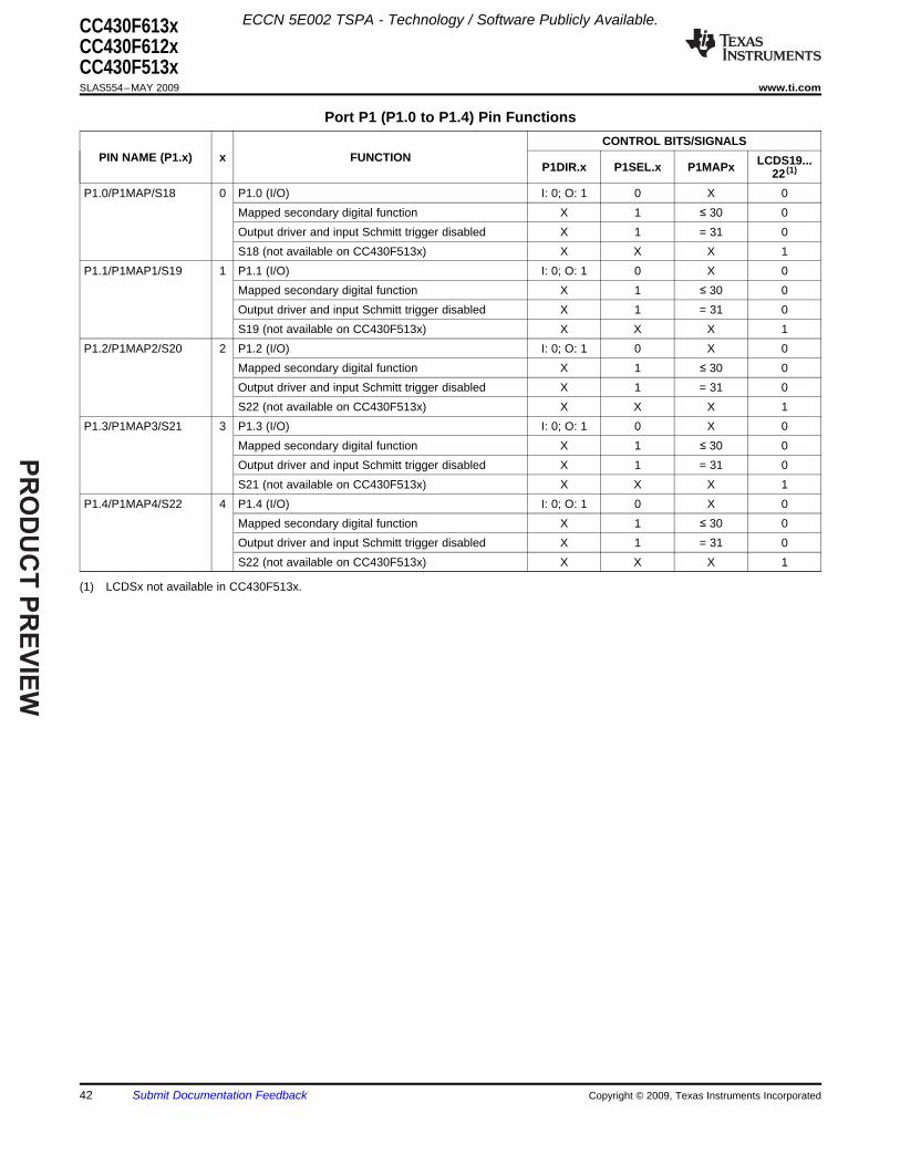
PR
OD
UC
T P
RE
VIE
W
ECCN 5E002 TSPA - Technology / Software Publicly Available.CC430F613xCC430F612xCC430F513xSLAS554–MAY 2009 ........................................................................................................................................................................................................ www.ti.com
Port P1 (P1.0 to P1.4) Pin FunctionsCONTROL BITS/SIGNALS
PIN NAME (P1.x) x FUNCTION LCDS19...P1DIR.x P1SEL.x P1MAPx 22 (1)
P1.0/P1MAP/S18 0 P1.0 (I/O) I: 0; O: 1 0 X 0Mapped secondary digital function X 1 ≤ 30 0Output driver and input Schmitt trigger disabled X 1 = 31 0S18 (not available on CC430F513x) X X X 1
P1.1/P1MAP1/S19 1 P1.1 (I/O) I: 0; O: 1 0 X 0Mapped secondary digital function X 1 ≤ 30 0Output driver and input Schmitt trigger disabled X 1 = 31 0S19 (not available on CC430F513x) X X X 1
P1.2/P1MAP2/S20 2 P1.2 (I/O) I: 0; O: 1 0 X 0Mapped secondary digital function X 1 ≤ 30 0Output driver and input Schmitt trigger disabled X 1 = 31 0S22 (not available on CC430F513x) X X X 1
P1.3/P1MAP3/S21 3 P1.3 (I/O) I: 0; O: 1 0 X 0Mapped secondary digital function X 1 ≤ 30 0Output driver and input Schmitt trigger disabled X 1 = 31 0S21 (not available on CC430F513x) X X X 1
P1.4/P1MAP4/S22 4 P1.4 (I/O) I: 0; O: 1 0 X 0Mapped secondary digital function X 1 ≤ 30 0Output driver and input Schmitt trigger disabled X 1 = 31 0S22 (not available on CC430F513x) X X X 1
(1) LCDSx not available in CC430F513x.
42 Submit Documentation Feedback Copyright © 2009, Texas Instruments Incorporated
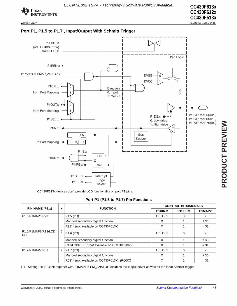
PR
OD
UC
T P
RE
VIE
W
Port P1, P1.5 to P1.7 , Input/Output With Schmitt Trigger
P1.5/P1MAP5(/R23)
P1.6/P1MAP6(/R13)
P1.7/P1MAP7(/R03)P1SEL.x
1
0P1DIR.x
P1IN.x
P1IRQ.x
EN
to Port Mapping
1
0
from Port Mapping
P1OUT.x
Interrupt
Select
Edge
Q
EN
Set
P1 .SEL x
P1IES x.
P1IFG.x
P1IE.x
1
0DVSS
DVCC 1
P1DS.x
0: Low drive
1: High drive
D
from Port Mapping
to LCD_B
from LCD_B
Pad Logic
Bus
Keeper
Direction
0: Input
1: Output
P1REN.x
P1MAP.x = PMAP_ANALOG
(n/a CC430F513x)
ECCN 5E002 TSPA - Technology / Software Publicly Available. CC430F613xCC430F612xCC430F513x
www.ti.com ........................................................................................................................................................................................................ SLAS554–MAY 2009
CC430F513x devices don't provide LCD functionality on port P1 pins.
Port P1 (P1.5 to P1.7) Pin FunctionsCONTROL BITS/SIGNALS
PIN NAME (P1.x) x FUNCTIONP1DIR.x P1SEL.x P1MAPx
P1.5/P1MAP5/R23 5 P1.5 (I/O) I: 0; O: 1 0 XMapped secondary digital function X 1 ≤ 30R23 (1) (not available on CC430F513x) X 1 = 31
P1.6/P1MAP6/R13/LCD 6 P1.6 (I/O) I: 0; O: 1 0 XREFMapped secondary digital function X 1 ≤ 30R13/LCDREF (1) (not available on CC430F513x) X 1 = 31
P1.7/P1MAP7/R03 7 P1.7 (I/O) I: 0; O: 1 0 XMapped secondary digital function X 1 ≤ 30R03 (1) (not available on CC430F513x), (ROSC) X 1 = 31
(1) Setting P1SEL.x bit together with P1MAPx = PM_ANALOG disables the output driver as well as the input Schmitt trigger.
Copyright © 2009, Texas Instruments Incorporated Submit Documentation Feedback 43
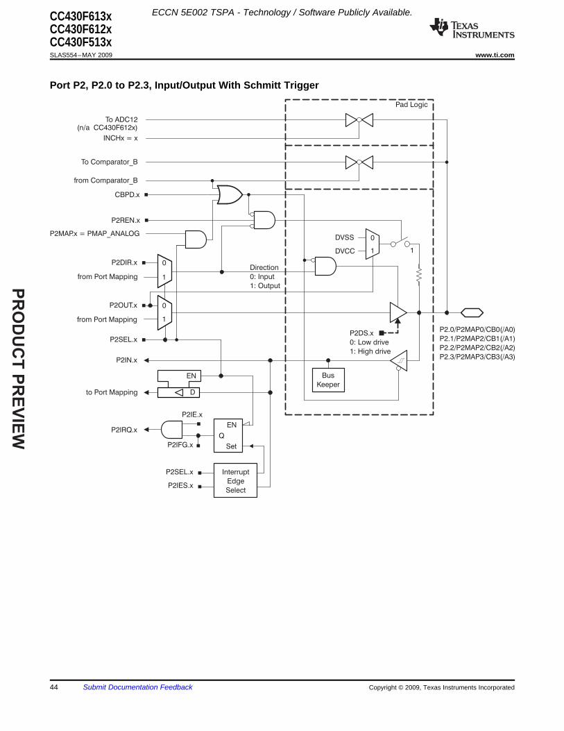
PR
OD
UC
T P
RE
VIE
W
Port P2, P2.0 to P2.3, Input/Output With Schmitt Trigger
P2.0/P2MAP0/CB0(/A0)
P2.1/P2MAP2/CB1(/A1)
P2.2/P2MAP2/CB2(/A2)
P2.3/P2MAP3/CB3(/A3)
Direction
0: Input
1: Output
P2SEL.x
1
0P2DIR.x
P2IN.x
P2IRQ.x
EN
to Port Mapping
1
0
from Port Mapping
P2OUT.x
Interrupt
Select
Edge
Q
EN
Set
P2 .SEL x
P2IES x.
P2IFG.x
P2IE.x
1
0DVSS
DVCC 1
P2DS.x
0: Low drive
1: High drive
D
from Port Mapping
To Comparator_B
from Comparator_B
Pad Logic
To ADC12
INCHx = x
(n/a CC430F612x)
CBPD.x
P2REN.x
P2MAP.x = PMAP_ANALOG
Bus
Keeper
ECCN 5E002 TSPA - Technology / Software Publicly Available.CC430F613xCC430F612xCC430F513xSLAS554–MAY 2009 ........................................................................................................................................................................................................ www.ti.com
44 Submit Documentation Feedback Copyright © 2009, Texas Instruments Incorporated
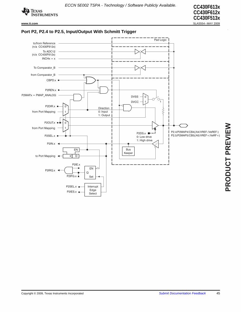
PR
OD
UC
T P
RE
VIE
W
Port P2, P2.4 to P2.5, Input/Output With Schmitt Trigger
P2.4/P2MAP4/CB4(/A4/VREF-/VeREF-)
P2.5/P2MAP5/CB5(/A5/VREF+/VeRF+)P2SEL.x
1
0P2DIR.x
P2IN.x
P2IRQ.x
EN
to Port Mapping
1
0
from Port Mapping
P2OUT.x
Interrupt
Select
Edge
Q
EN
Set
P2 .SEL x
P2IES x.
P2IFG.x
P2IE.x
1
0DVSS
DVCC 1
P2DS.x
0: Low drive
1: High drive
D
from Port Mapping
To Comparator_B
from Comparator_B
Pad Logic
To ADC12
INCHx = x
(n/a CC430F612x)
Bus
Keeper
to/from Reference
(n/a CC430F612x)
Direction
0: Input
1: Output
CBPD.x
P2REN.x
P2MAP.x = PMAP_ANALOG
ECCN 5E002 TSPA - Technology / Software Publicly Available. CC430F613xCC430F612xCC430F513x
www.ti.com ........................................................................................................................................................................................................ SLAS554–MAY 2009
Copyright © 2009, Texas Instruments Incorporated Submit Documentation Feedback 45
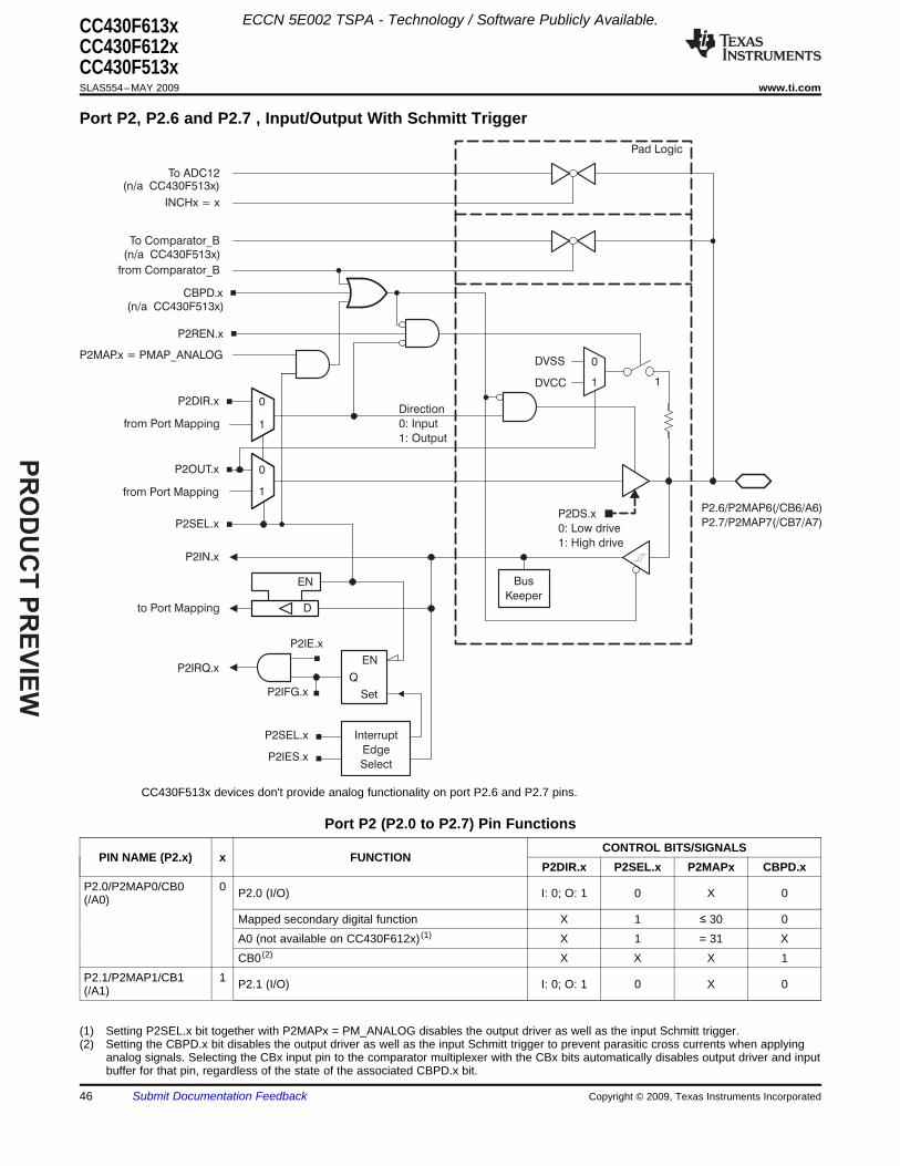
PR
OD
UC
T P
RE
VIE
W
Port P2, P2.6 and P2.7 , Input/Output With Schmitt Trigger
P2.6/P2MAP6(/CB6/A6)
P2.7/P2MAP7(/CB7/A7)
Direction
0: Input
1: Output
P2SEL.x
1
0P2DIR.x
P2IN.x
P2IRQ.x
EN
to Port Mapping
1
0
from Port Mapping
P2OUT.x
Interrupt
Select
Edge
Q
EN
Set
P2 .SEL x
P2IES x.
P2IFG.x
P2IE.x
1
0DVSS
DVCC 1
P2DS.x
0: Low drive
1: High drive
D
from Port Mapping
To Comparator_B
from Comparator_B
Pad Logic
To ADC12
INCHx = x
(n/a CC430F513x)
(n/a CC430F513x)
(n/a CC430F513x)CBPD.x
P2REN.x
P2MAP.x = PMAP_ANALOG
Bus
Keeper
ECCN 5E002 TSPA - Technology / Software Publicly Available.CC430F613xCC430F612xCC430F513xSLAS554–MAY 2009 ........................................................................................................................................................................................................ www.ti.com
CC430F513x devices don't provide analog functionality on port P2.6 and P2.7 pins.
Port P2 (P2.0 to P2.7) Pin FunctionsCONTROL BITS/SIGNALS
PIN NAME (P2.x) x FUNCTIONP2DIR.x P2SEL.x P2MAPx CBPD.x
P2.0/P2MAP0/CB0 0 P2.0 (I/O) I: 0; O: 1 0 X 0(/A0)Mapped secondary digital function X 1 ≤ 30 0A0 (not available on CC430F612x) (1) X 1 = 31 XCB0 (2) X X X 1
P2.1/P2MAP1/CB1 1 P2.1 (I/O) I: 0; O: 1 0 X 0(/A1)
(1) Setting P2SEL.x bit together with P2MAPx = PM_ANALOG disables the output driver as well as the input Schmitt trigger.(2) Setting the CBPD.x bit disables the output driver as well as the input Schmitt trigger to prevent parasitic cross currents when applying
analog signals. Selecting the CBx input pin to the comparator multiplexer with the CBx bits automatically disables output driver and inputbuffer for that pin, regardless of the state of the associated CBPD.x bit.
46 Submit Documentation Feedback Copyright © 2009, Texas Instruments Incorporated
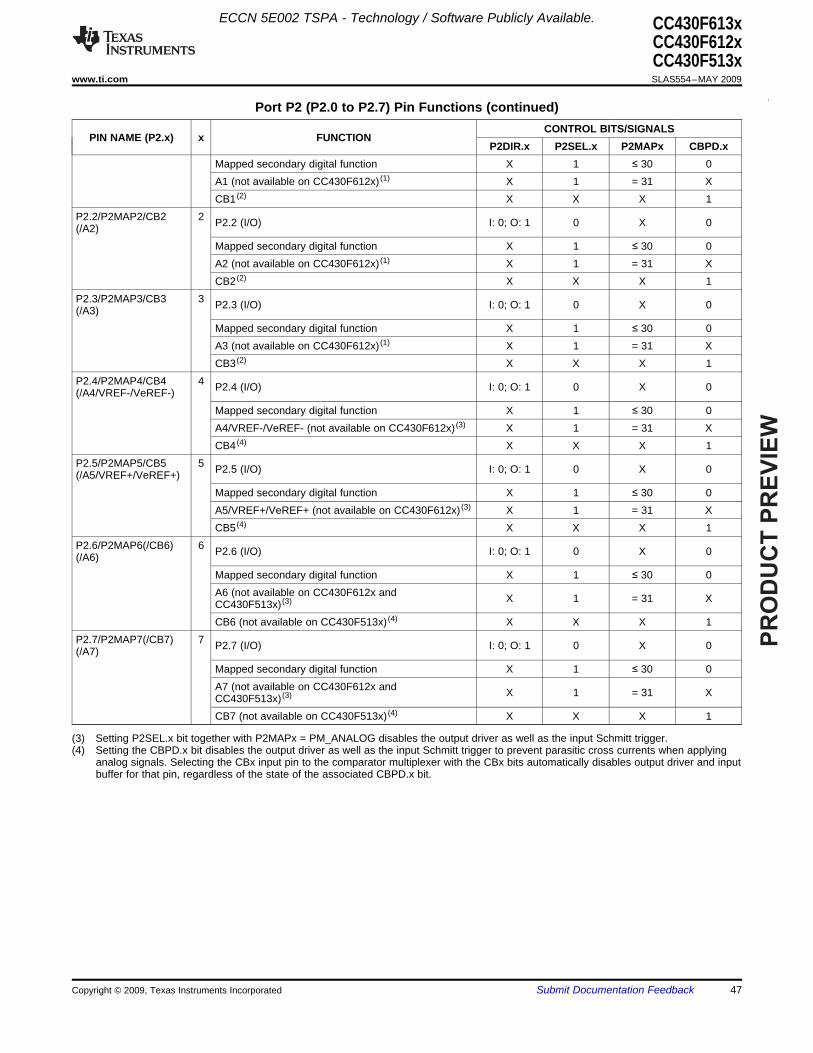
PR
OD
UC
T P
RE
VIE
W
ECCN 5E002 TSPA - Technology / Software Publicly Available. CC430F613xCC430F612xCC430F513x
www.ti.com ........................................................................................................................................................................................................ SLAS554–MAY 2009
Port P2 (P2.0 to P2.7) Pin Functions (continued)CONTROL BITS/SIGNALS
PIN NAME (P2.x) x FUNCTIONP2DIR.x P2SEL.x P2MAPx CBPD.x
Mapped secondary digital function X 1 ≤ 30 0A1 (not available on CC430F612x) (1) X 1 = 31 XCB1 (2) X X X 1
P2.2/P2MAP2/CB2 2 P2.2 (I/O) I: 0; O: 1 0 X 0(/A2)Mapped secondary digital function X 1 ≤ 30 0A2 (not available on CC430F612x) (1) X 1 = 31 XCB2 (2) X X X 1
P2.3/P2MAP3/CB3 3 P2.3 (I/O) I: 0; O: 1 0 X 0(/A3)Mapped secondary digital function X 1 ≤ 30 0A3 (not available on CC430F612x) (1) X 1 = 31 XCB3 (2) X X X 1
P2.4/P2MAP4/CB4 4 P2.4 (I/O) I: 0; O: 1 0 X 0(/A4/VREF-/VeREF-)Mapped secondary digital function X 1 ≤ 30 0A4/VREF-/VeREF- (not available on CC430F612x) (3) X 1 = 31 XCB4 (4) X X X 1
P2.5/P2MAP5/CB5 5 P2.5 (I/O) I: 0; O: 1 0 X 0(/A5/VREF+/VeREF+)Mapped secondary digital function X 1 ≤ 30 0A5/VREF+/VeREF+ (not available on CC430F612x) (3) X 1 = 31 XCB5 (4) X X X 1
P2.6/P2MAP6(/CB6) 6 P2.6 (I/O) I: 0; O: 1 0 X 0(/A6)Mapped secondary digital function X 1 ≤ 30 0A6 (not available on CC430F612x and X 1 = 31 XCC430F513x) (3)
CB6 (not available on CC430F513x) (4) X X X 1P2.7/P2MAP7(/CB7) 7 P2.7 (I/O) I: 0; O: 1 0 X 0(/A7)
Mapped secondary digital function X 1 ≤ 30 0A7 (not available on CC430F612x and X 1 = 31 XCC430F513x) (3)
CB7 (not available on CC430F513x) (4) X X X 1
(3) Setting P2SEL.x bit together with P2MAPx = PM_ANALOG disables the output driver as well as the input Schmitt trigger.(4) Setting the CBPD.x bit disables the output driver as well as the input Schmitt trigger to prevent parasitic cross currents when applying
analog signals. Selecting the CBx input pin to the comparator multiplexer with the CBx bits automatically disables output driver and inputbuffer for that pin, regardless of the state of the associated CBPD.x bit.
Copyright © 2009, Texas Instruments Incorporated Submit Documentation Feedback 47
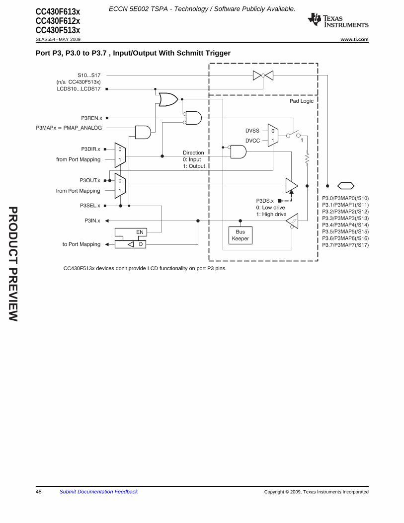
PR
OD
UC
T P
RE
VIE
W
Port P3, P3.0 to P3.7 , Input/Output With Schmitt Trigger
P3.4/P3MAP4(/S14)
P3.5/P3MAP5(/S15)
P3.6/P3MAP6(/S16)
P3.7/P3MAP7(/S17)
P3.0/P3MAP0(/S10)
P3.1/P3MAP1(/S11)
P3.2/P3MAP2(/S12)
P3.3/P3MAP3(/S13)
Direction
0: Input
1: Output
P3SEL.x
1
0P3DIR.x
P3IN.x
EN
to Port Mapping
1
0
from Port Mapping
P3OUT.x
1
0DVSS
DVCC 1
P3DS.x
0: Low drive
1: High drive
D
from Port Mapping
S10...S17
LCDS10...LCDS17
Pad Logic
P3REN.x
P3MAP.x = PMAP_ANALOG
Bus
Keeper
(n/a CC430F513x)
ECCN 5E002 TSPA - Technology / Software Publicly Available.CC430F613xCC430F612xCC430F513xSLAS554–MAY 2009 ........................................................................................................................................................................................................ www.ti.com
CC430F513x devices don't provide LCD functionality on port P3 pins.
48 Submit Documentation Feedback Copyright © 2009, Texas Instruments Incorporated
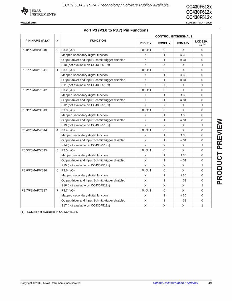
PR
OD
UC
T P
RE
VIE
W
ECCN 5E002 TSPA - Technology / Software Publicly Available. CC430F613xCC430F612xCC430F513x
www.ti.com ........................................................................................................................................................................................................ SLAS554–MAY 2009
Port P3 (P3.0 to P3.7) Pin FunctionsCONTROL BITS/SIGNALS
PIN NAME (P3.x) x FUNCTION LCDS10...P3DIR.x P3SEL.x P3MAPx 17 (1)
P3.0/P3MAP0/S10 0 P3.0 (I/O) I: 0; O: 1 0 X 0Mapped secondary digital function X 1 ≤ 30 0Output driver and input Schmitt trigger disabled X 1 = 31 0S10 (not available on CC430F513x) X X X 1
P3.1/P3MAP1/S11 1 P3.1 (I/O) I: 0; O: 1 0 X 0Mapped secondary digital function X 1 ≤ 30 0Output driver and input Schmitt trigger disabled X 1 = 31 0S11 (not available on CC430F513x) X X X 1
P3.2/P3MAP7/S12 2 P3.2 (I/O) I: 0; O: 1 0 X 0Mapped secondary digital function X 1 ≤ 30 0Output driver and input Schmitt trigger disabled X 1 = 31 0S12 (not available on CC430F513x) X X X 1
P3.3/P3MAP3/S13 3 P3.3 (I/O) I: 0; O: 1 0 X 0Mapped secondary digital function X 1 ≤ 30 0Output driver and input Schmitt trigger disabled X 1 = 31 0S13 (not available on CC430F513x) X X X 1
P3.4/P3MAP4/S14 4 P3.4 (I/O) I: 0; O: 1 0 X 0Mapped secondary digital function X 1 ≤ 30 0Output driver and input Schmitt trigger disabled X 1 = 31 0S14 (not available on CC430F513x) X X X 1
P3.5/P3MAP5/S15 5 P3.5 (I/O) I: 0; O: 1 0 X 0Mapped secondary digital function X 1 ≤ 30 0Output driver and input Schmitt trigger disabled X 1 = 31 0S15 (not available on CC430F513x) X X X 1
P3.6/P3MAP6/S16 6 P3.6 (I/O) I: 0; O: 1 0 X 0Mapped secondary digital function X 1 ≤ 30 0Output driver and input Schmitt trigger disabled X 1 = 31 0S16 (not available on CC430F513x) X X X 1
P3.7/P3MAP7/S17 7 P3.7 (I/O) I: 0; O: 1 0 X 0Mapped secondary digital function X 1 ≤ 30 0Output driver and input Schmitt trigger disabled X 1 = 31 0S17 (not available on CC430F513x) X X X 1
(1) LCDSx not available in CC430F513x.
Copyright © 2009, Texas Instruments Incorporated Submit Documentation Feedback 49
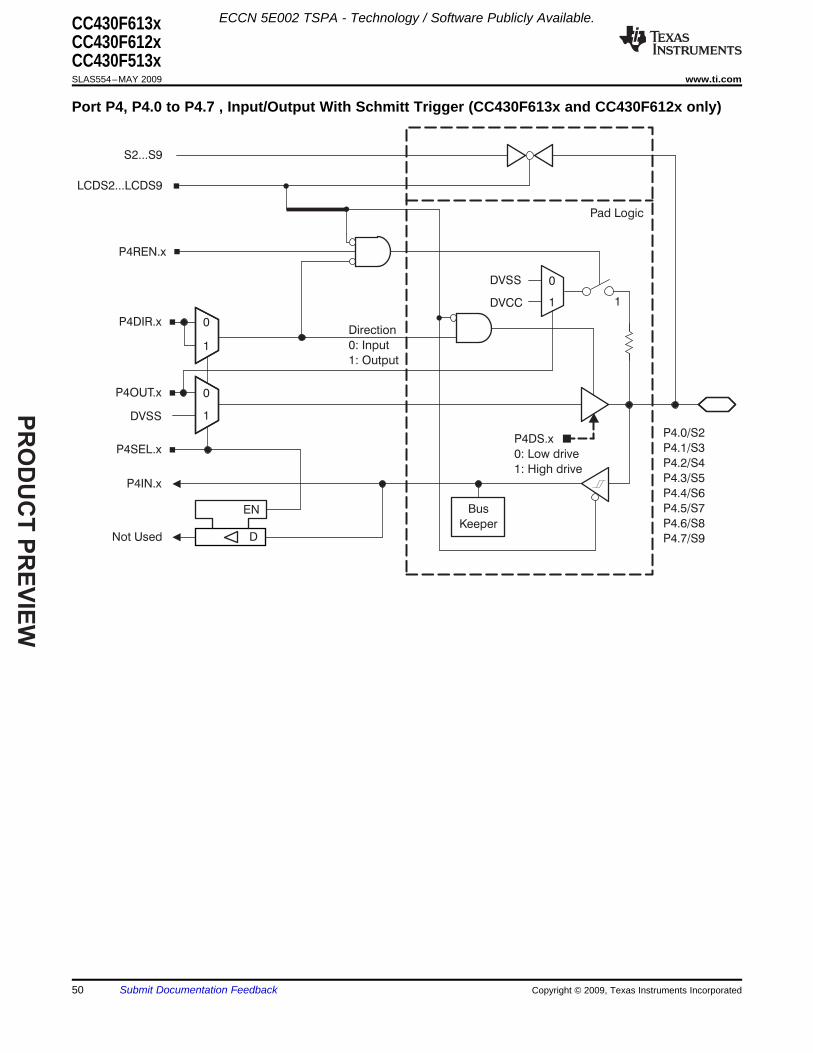
PR
OD
UC
T P
RE
VIE
W
Port P4, P4.0 to P4.7 , Input/Output With Schmitt Trigger (CC430F613x and CC430F612x only)
P4.4/S6
P4.5/S7
P4.6/S8
P4.7/S9
P4.0/S2
P4.1/S3
P4.2/S4
P4.3/S5
Direction
0: Input
1: Output
P4SEL.x
1
0P4DIR.x
P4IN.x
EN
Not Used
1
0
DVSS
P4OUT.x
1
0DVSS
DVCC 1
P4DS.x
0: Low drive
1: High drive
D
S2...S9
LCDS2...LCDS9
Pad Logic
P4REN.x
Bus
Keeper
ECCN 5E002 TSPA - Technology / Software Publicly Available.CC430F613xCC430F612xCC430F513xSLAS554–MAY 2009 ........................................................................................................................................................................................................ www.ti.com
50 Submit Documentation Feedback Copyright © 2009, Texas Instruments Incorporated
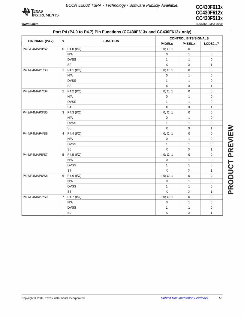
PR
OD
UC
T P
RE
VIE
W
ECCN 5E002 TSPA - Technology / Software Publicly Available. CC430F613xCC430F612xCC430F513x
www.ti.com ........................................................................................................................................................................................................ SLAS554–MAY 2009
Port P4 (P4.0 to P4.7) Pin Functions (CC430F613x and CC430F612x only)CONTROL BITS/SIGNALS
PIN NAME (P4.x) x FUNCTIONP4DIR.x P4SEL.x LCDS2...7
P4.0/P4MAP0/S2 0 P4.0 (I/O) I: 0; O: 1 0 0N/A 0 1 0DVSS 1 1 0S2 X X 1
P4.1/P4MAP1/S3 1 P4.1 (I/O) I: 0; O: 1 0 0N/A 0 1 0DVSS 1 1 0S3 X X 1
P4.2/P4MAP7/S4 2 P4.2 (I/O) I: 0; O: 1 0 0N/A 0 1 0DVSS 1 1 0S4 X X 1
P4.3/P4MAP3/S5 3 P4.3 (I/O) I: 0; O: 1 0 0N/A 0 1 0DVSS 1 1 0S5 X X 1
P4.4/P4MAP4/S6 4 P4.4 (I/O) I: 0; O: 1 0 0N/A 0 1 0DVSS 1 1 0S6 X X 1
P4.5/P4MAP5/S7 5 P4.5 (I/O) I: 0; O: 1 0 0N/A 0 1 0DVSS 1 1 0S7 X X 1
P4.6/P4MAP6/S8 6 P4.6 (I/O) I: 0; O: 1 0 0N/A 0 1 0DVSS 1 1 0S8 X X 1
P4.7/P4MAP7/S9 7 P4.7 (I/O) I: 0; O: 1 0 0N/A 0 1 0DVSS 1 1 0S9 X X 1
Copyright © 2009, Texas Instruments Incorporated Submit Documentation Feedback 51
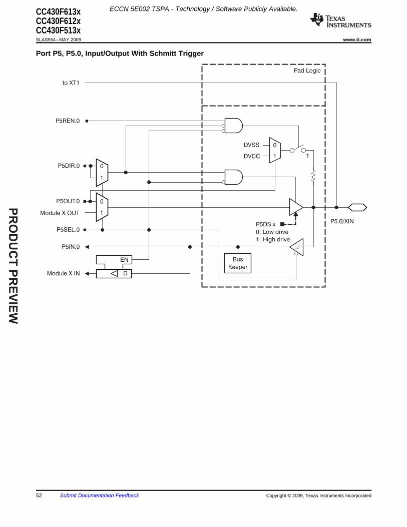
PR
OD
UC
T P
RE
VIE
W
Port P5, P5.0, Input/Output With Schmitt Trigger
P5.0/XIN
P5SEL.0
1
0P5DIR.0
P5IN.0
EN
Module X IN
1
0
Module X OUT
P5OUT.0
1
0DVSS
DVCC
P5REN.0
Pad Logic
1
P5DS.x
0: Low drive
1: High drive
D
Bus
Keeper
to XT1
ECCN 5E002 TSPA - Technology / Software Publicly Available.CC430F613xCC430F612xCC430F513xSLAS554–MAY 2009 ........................................................................................................................................................................................................ www.ti.com
52 Submit Documentation Feedback Copyright © 2009, Texas Instruments Incorporated
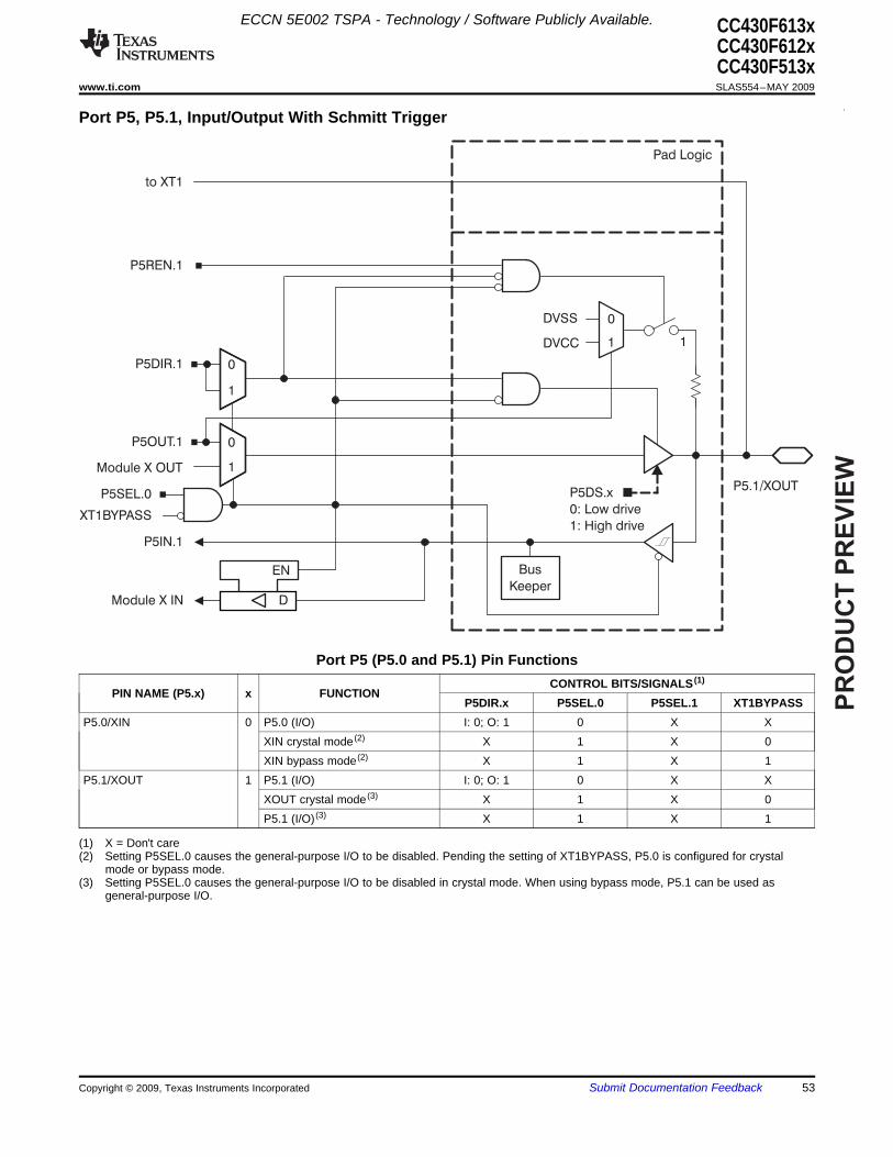
PR
OD
UC
T P
RE
VIE
W
Port P5, P5.1, Input/Output With Schmitt Trigger
P5.1/XOUTP5SEL.0
XT1BYPASS
1
0P5DIR.1
P5IN.1
EN
Module X IN
1
0
Module X OUT
P5OUT.1
1
0DVSS
DVCC
P5REN.1
Pad Logic
1
P5DS.x
0: Low drive
1: High drive
D
Bus
Keeper
to XT1
ECCN 5E002 TSPA - Technology / Software Publicly Available. CC430F613xCC430F612xCC430F513x
www.ti.com ........................................................................................................................................................................................................ SLAS554–MAY 2009
Port P5 (P5.0 and P5.1) Pin FunctionsCONTROL BITS/SIGNALS (1)
PIN NAME (P5.x) x FUNCTIONP5DIR.x P5SEL.0 P5SEL.1 XT1BYPASS
P5.0/XIN 0 P5.0 (I/O) I: 0; O: 1 0 X XXIN crystal mode (2) X 1 X 0XIN bypass mode (2) X 1 X 1
P5.1/XOUT 1 P5.1 (I/O) I: 0; O: 1 0 X XXOUT crystal mode (3) X 1 X 0P5.1 (I/O) (3) X 1 X 1
(1) X = Don't care(2) Setting P5SEL.0 causes the general-purpose I/O to be disabled. Pending the setting of XT1BYPASS, P5.0 is configured for crystal
mode or bypass mode.(3) Setting P5SEL.0 causes the general-purpose I/O to be disabled in crystal mode. When using bypass mode, P5.1 can be used as
general-purpose I/O.
Copyright © 2009, Texas Instruments Incorporated Submit Documentation Feedback 53
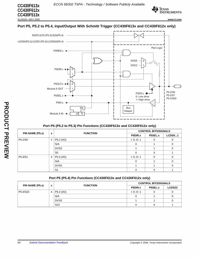
PR
OD
UC
T P
RE
VIE
W
Port P5, P5.2 to P5.4, Input/Output With Schmitt Trigger (CC430F613x and CC430F612x only)
P5.2/S0
P5.3/S1
P5.4/S23P5SEL.x
1
0P5DIR.x
P5IN.x
EN
Module X IN
1
0
Module X OUT
P5OUT.x
1
0DVSS
DVCC
P5REN.xPad Logic
1
P5DS.x
0: Low drive
1: High drive
D
Bus
Keeper
S0(P5.2)/S1(P5.3)/S23(P5.4)
LCDS0(P5.2)/LCDS1(P5.3)/LCDS23(P5.4)
ECCN 5E002 TSPA - Technology / Software Publicly Available.CC430F613xCC430F612xCC430F513xSLAS554–MAY 2009 ........................................................................................................................................................................................................ www.ti.com
Port P5 (P5.2 to P5.3) Pin Functions (CC430F613x and CC430F612x only)CONTROL BITS/SIGNALS
PIN NAME (P5.x) x FUNCTIONP5DIR.x P5SEL.x LCDS0...1
P5.2/S0 2 P5.2 (I/O) I: 0; O: 1 0 0N/A 0 1 0DVSS 1 1 0S0 X X 1
P5.3/S1 3 P5.3 (I/O) I: 0; O: 1 0 0N/A 0 1 0DVSS 1 1 0S1 X X 1
Port P5 (P5.4) Pin Functions (CC430F613x and CC430F612x only)CONTROL BITS/SIGNALS
PIN NAME (P5.x) x FUNCTIONP5DIR.x P5SEL.x LCDS23
P5.4/S23 4 P5.4 (I/O) I: 0; O: 1 0 0N/A 0 1 0DVSS 1 1 0S23 X X 1
54 Submit Documentation Feedback Copyright © 2009, Texas Instruments Incorporated
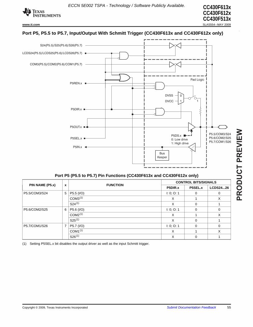
PR
OD
UC
T P
RE
VIE
W
Port P5, P5.5 to P5.7, Input/Output With Schmitt Trigger (CC430F613x and CC430F612x only)
P5.5/COM3/S24
P5.6/COM2/S25
P5.7/COM1/S26P5SEL.x
P5DIR.x
P5IN.x
P5OUT.x
1
0DVSS
DVCC
P5REN.xPad Logic
1
P5DS.x
0: Low drive
1: High drive
Bus
Keeper
COM3(P5.5)/COM2(P5.6)/COM1(P5.7)
S24(P5.5)/S25(P5.6)/S26(P5.7)
LCDS24(P5.5)/LCDS25(P5.6)/LCDS26(P5.7)
ECCN 5E002 TSPA - Technology / Software Publicly Available. CC430F613xCC430F612xCC430F513x
www.ti.com ........................................................................................................................................................................................................ SLAS554–MAY 2009
Port P5 (P5.5 to P5.7) Pin Functions (CC430F613x and CC430F612x only)CONTROL BITS/SIGNALS
PIN NAME (P5.x) x FUNCTIONP5DIR.x P5SEL.x LCDS24...26
P5.5/COM3/S24 5 P5.5 (I/O) I: 0; O: 1 0 0COM3 (1) X 1 XS24 (1) X 0 1
P5.6/COM2/S25 6 P5.6 (I/O) I: 0; O: 1 0 0COM2 (1) X 1 XS25 (1) X 0 1
P5.7/COM1/S26 7 P5.7 (I/O) I: 0; O: 1 0 0COM1 (1) X 1 XS26 (1) X 0 1
(1) Setting P5SEL.x bit disables the output driver as well as the input Schmitt trigger.
Copyright © 2009, Texas Instruments Incorporated Submit Documentation Feedback 55
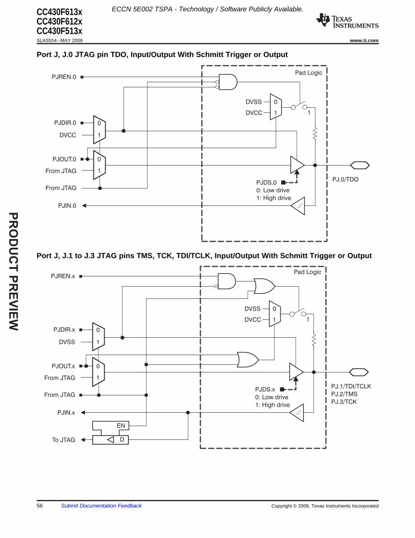
PR
OD
UC
T P
RE
VIE
W
Port J, J.0 JTAG pin TDO, Input/Output With Schmitt Trigger or Output
PJ.0/TDO
From JTAG
1
0PJDIR.0
PJIN.0
1
0
From JTAG
PJOUT.0
1
0DVSS
DVCC
PJREN.0Pad Logic
1
PJDS.0
0: Low drive
1: High drive
DVCC
Port J, J.1 to J.3 JTAG pins TMS, TCK, TDI/TCLK, Input/Output With Schmitt Trigger or Output
PJ.1/TDI/TCLK
PJ.2/TMS
PJ.3/TCKFrom JTAG
1
0PJDIR.x
PJIN.x
EN
1
0
From JTAG
PJOUT.x
1
0DVSS
DVCC
PJREN.xPad Logic
1
PJDS.x
0: Low drive
1: High drive
D
DVSS
To JTAG
ECCN 5E002 TSPA - Technology / Software Publicly Available.CC430F613xCC430F612xCC430F513xSLAS554–MAY 2009 ........................................................................................................................................................................................................ www.ti.com
56 Submit Documentation Feedback Copyright © 2009, Texas Instruments Incorporated

PR
OD
UC
T P
RE
VIE
W
ECCN 5E002 TSPA - Technology / Software Publicly Available. CC430F613xCC430F612xCC430F513x
www.ti.com ........................................................................................................................................................................................................ SLAS554–MAY 2009
Port PJ (PJ.0 to PJ.3) Pin FunctionsCONTROL BITS/
SIGNALS (1)PIN NAME (PJ.x) x FUNCTIONPJDIR.x
PJ.0/TDO 0 PJ.0 (I/O) (2) I: 0; O: 1TDO (3) X
PJ.1/TDI/TCLK 1 PJ.1 (I/O) (2) I: 0; O: 1TDI/TCLK (3) (4) X
PJ.2/TMS 2 PJ.2 (I/O) (2) I: 0; O: 1TMS (3) (4) X
PJ.3/TCK 3 PJ.3 (I/O) (2) I: 0; O: 1TCK (3) (4) X
(1) X = Don't care(2) Default condition(3) The pin direction is controlled by the JTAG module.(4) In JTAG mode, pullups are activated automatically on TMS, TCK, and TDI/TCLK. PJREN.x are do not care.
Copyright © 2009, Texas Instruments Incorporated Submit Documentation Feedback 57
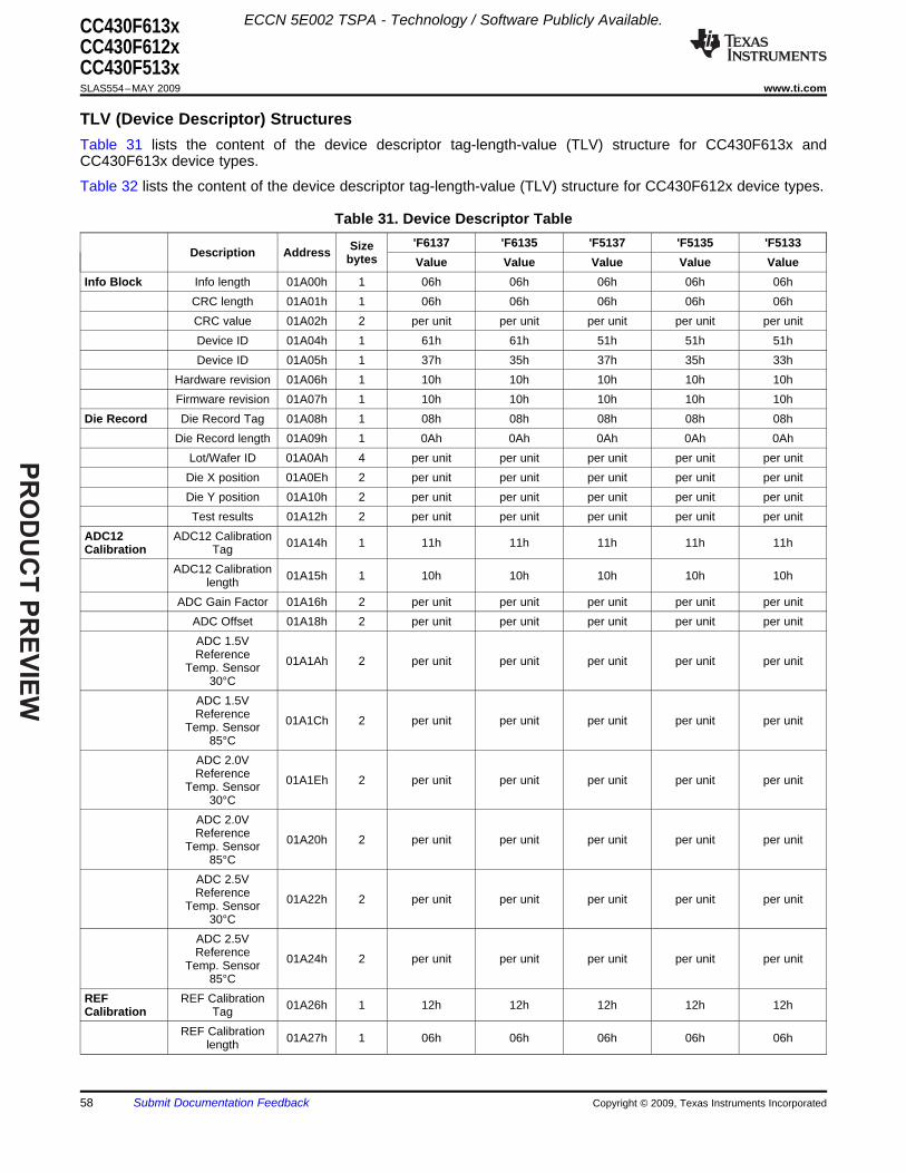
PR
OD
UC
T P
RE
VIE
W
TLV (Device Descriptor) Structures
ECCN 5E002 TSPA - Technology / Software Publicly Available.CC430F613xCC430F612xCC430F513xSLAS554–MAY 2009 ........................................................................................................................................................................................................ www.ti.com
Table 31 lists the content of the device descriptor tag-length-value (TLV) structure for CC430F613x andCC430F613x device types.
Table 32 lists the content of the device descriptor tag-length-value (TLV) structure for CC430F612x device types.
Table 31. Device Descriptor Table'F6137 'F6135 'F5137 'F5135 'F5133SizeDescription Address bytes Value Value Value Value Value
Info Block Info length 01A00h 1 06h 06h 06h 06h 06hCRC length 01A01h 1 06h 06h 06h 06h 06hCRC value 01A02h 2 per unit per unit per unit per unit per unitDevice ID 01A04h 1 61h 61h 51h 51h 51hDevice ID 01A05h 1 37h 35h 37h 35h 33h
Hardware revision 01A06h 1 10h 10h 10h 10h 10hFirmware revision 01A07h 1 10h 10h 10h 10h 10h
Die Record Die Record Tag 01A08h 1 08h 08h 08h 08h 08hDie Record length 01A09h 1 0Ah 0Ah 0Ah 0Ah 0Ah
Lot/Wafer ID 01A0Ah 4 per unit per unit per unit per unit per unitDie X position 01A0Eh 2 per unit per unit per unit per unit per unitDie Y position 01A10h 2 per unit per unit per unit per unit per unitTest results 01A12h 2 per unit per unit per unit per unit per unit
ADC12 ADC12 Calibration 01A14h 1 11h 11h 11h 11h 11hCalibration TagADC12 Calibration 01A15h 1 10h 10h 10h 10h 10hlengthADC Gain Factor 01A16h 2 per unit per unit per unit per unit per unit
ADC Offset 01A18h 2 per unit per unit per unit per unit per unitADC 1.5VReference 01A1Ah 2 per unit per unit per unit per unit per unitTemp. Sensor
30°CADC 1.5VReference 01A1Ch 2 per unit per unit per unit per unit per unitTemp. Sensor
85°CADC 2.0VReference 01A1Eh 2 per unit per unit per unit per unit per unitTemp. Sensor
30°CADC 2.0VReference 01A20h 2 per unit per unit per unit per unit per unitTemp. Sensor
85°CADC 2.5VReference 01A22h 2 per unit per unit per unit per unit per unitTemp. Sensor
30°CADC 2.5VReference 01A24h 2 per unit per unit per unit per unit per unitTemp. Sensor
85°CREF REF Calibration 01A26h 1 12h 12h 12h 12h 12hCalibration Tag
REF Calibration 01A27h 1 06h 06h 06h 06h 06hlength
58 Submit Documentation Feedback Copyright © 2009, Texas Instruments Incorporated
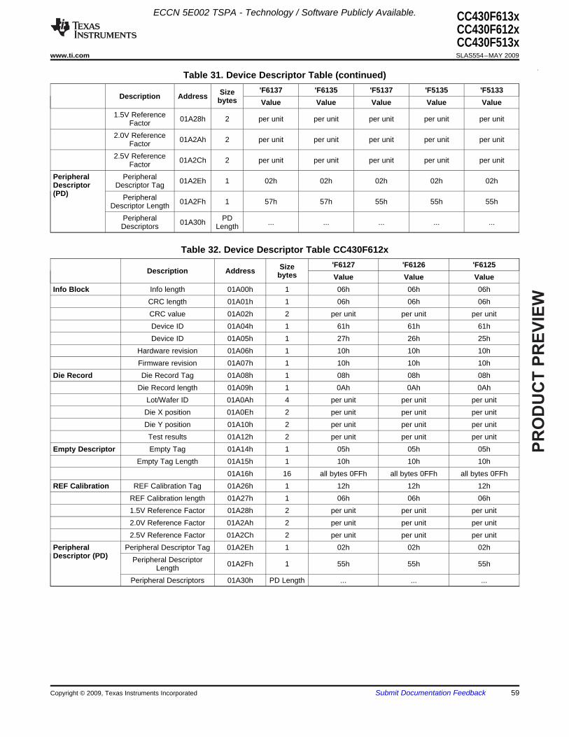
PR
OD
UC
T P
RE
VIE
W
ECCN 5E002 TSPA - Technology / Software Publicly Available. CC430F613xCC430F612xCC430F513x
www.ti.com ........................................................................................................................................................................................................ SLAS554–MAY 2009
Table 31. Device Descriptor Table (continued)'F6137 'F6135 'F5137 'F5135 'F5133SizeDescription Address bytes Value Value Value Value Value
1.5V Reference 01A28h 2 per unit per unit per unit per unit per unitFactor2.0V Reference 01A2Ah 2 per unit per unit per unit per unit per unitFactor2.5V Reference 01A2Ch 2 per unit per unit per unit per unit per unitFactor
Peripheral Peripheral 01A2Eh 1 02h 02h 02h 02h 02hDescriptor Descriptor Tag(PD) Peripheral 01A2Fh 1 57h 57h 55h 55h 55hDescriptor Length
Peripheral PD01A30h ... ... ... ... ...Descriptors Length
Table 32. Device Descriptor Table CC430F612x'F6127 'F6126 'F6125SizeDescription Address bytes Value Value Value
Info Block Info length 01A00h 1 06h 06h 06hCRC length 01A01h 1 06h 06h 06hCRC value 01A02h 2 per unit per unit per unitDevice ID 01A04h 1 61h 61h 61hDevice ID 01A05h 1 27h 26h 25h
Hardware revision 01A06h 1 10h 10h 10hFirmware revision 01A07h 1 10h 10h 10h
Die Record Die Record Tag 01A08h 1 08h 08h 08hDie Record length 01A09h 1 0Ah 0Ah 0Ah
Lot/Wafer ID 01A0Ah 4 per unit per unit per unitDie X position 01A0Eh 2 per unit per unit per unitDie Y position 01A10h 2 per unit per unit per unitTest results 01A12h 2 per unit per unit per unit
Empty Descriptor Empty Tag 01A14h 1 05h 05h 05hEmpty Tag Length 01A15h 1 10h 10h 10h
01A16h 16 all bytes 0FFh all bytes 0FFh all bytes 0FFhREF Calibration REF Calibration Tag 01A26h 1 12h 12h 12h
REF Calibration length 01A27h 1 06h 06h 06h1.5V Reference Factor 01A28h 2 per unit per unit per unit2.0V Reference Factor 01A2Ah 2 per unit per unit per unit2.5V Reference Factor 01A2Ch 2 per unit per unit per unit
Peripheral Peripheral Descriptor Tag 01A2Eh 1 02h 02h 02hDescriptor (PD) Peripheral Descriptor 01A2Fh 1 55h 55h 55hLength
Peripheral Descriptors 01A30h PD Length ... ... ...
Copyright © 2009, Texas Instruments Incorporated Submit Documentation Feedback 59
PR
OD
UC
T P
RE
VIE
W
ECCN 5E002 TSPA - Technology / Software Publicly Available.CC430F613xCC430F612xCC430F513xSLAS554–MAY 2009 ........................................................................................................................................................................................................ www.ti.com
Data Sheet Revision HistoryREVISION DESCRIPTIONSLAS554 Product Preview data sheet release
60 Submit Documentation Feedback Copyright © 2009, Texas Instruments Incorporated
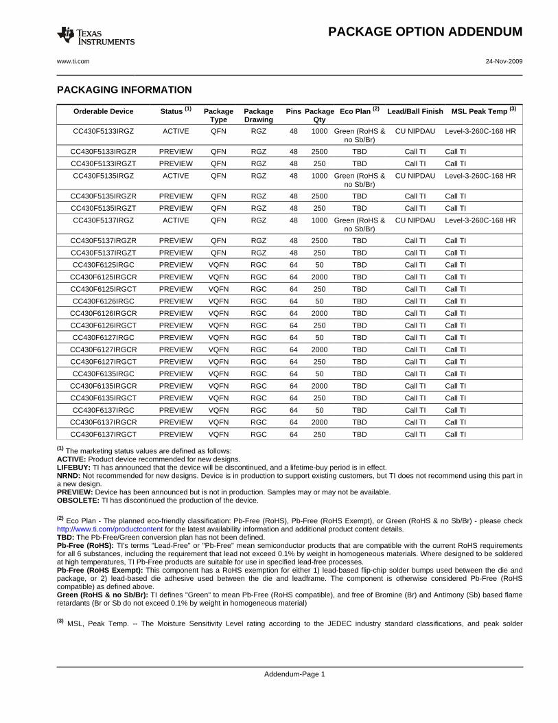
PACKAGING INFORMATION
Orderable Device Status (1) PackageType
PackageDrawing
Pins PackageQty
Eco Plan (2) Lead/Ball Finish MSL Peak Temp (3)
CC430F5133IRGZ ACTIVE QFN RGZ 48 1000 Green (RoHS &no Sb/Br)
CU NIPDAU Level-3-260C-168 HR
CC430F5133IRGZR PREVIEW QFN RGZ 48 2500 TBD Call TI Call TI
CC430F5133IRGZT PREVIEW QFN RGZ 48 250 TBD Call TI Call TI
CC430F5135IRGZ ACTIVE QFN RGZ 48 1000 Green (RoHS &no Sb/Br)
CU NIPDAU Level-3-260C-168 HR
CC430F5135IRGZR PREVIEW QFN RGZ 48 2500 TBD Call TI Call TI
CC430F5135IRGZT PREVIEW QFN RGZ 48 250 TBD Call TI Call TI
CC430F5137IRGZ ACTIVE QFN RGZ 48 1000 Green (RoHS &no Sb/Br)
CU NIPDAU Level-3-260C-168 HR
CC430F5137IRGZR PREVIEW QFN RGZ 48 2500 TBD Call TI Call TI
CC430F5137IRGZT PREVIEW QFN RGZ 48 250 TBD Call TI Call TI
CC430F6125IRGC PREVIEW VQFN RGC 64 50 TBD Call TI Call TI
CC430F6125IRGCR PREVIEW VQFN RGC 64 2000 TBD Call TI Call TI
CC430F6125IRGCT PREVIEW VQFN RGC 64 250 TBD Call TI Call TI
CC430F6126IRGC PREVIEW VQFN RGC 64 50 TBD Call TI Call TI
CC430F6126IRGCR PREVIEW VQFN RGC 64 2000 TBD Call TI Call TI
CC430F6126IRGCT PREVIEW VQFN RGC 64 250 TBD Call TI Call TI
CC430F6127IRGC PREVIEW VQFN RGC 64 50 TBD Call TI Call TI
CC430F6127IRGCR PREVIEW VQFN RGC 64 2000 TBD Call TI Call TI
CC430F6127IRGCT PREVIEW VQFN RGC 64 250 TBD Call TI Call TI
CC430F6135IRGC PREVIEW VQFN RGC 64 50 TBD Call TI Call TI
CC430F6135IRGCR PREVIEW VQFN RGC 64 2000 TBD Call TI Call TI
CC430F6135IRGCT PREVIEW VQFN RGC 64 250 TBD Call TI Call TI
CC430F6137IRGC PREVIEW VQFN RGC 64 50 TBD Call TI Call TI
CC430F6137IRGCR PREVIEW VQFN RGC 64 2000 TBD Call TI Call TI
CC430F6137IRGCT PREVIEW VQFN RGC 64 250 TBD Call TI Call TI
(1) The marketing status values are defined as follows:ACTIVE: Product device recommended for new designs.LIFEBUY: TI has announced that the device will be discontinued, and a lifetime-buy period is in effect.NRND: Not recommended for new designs. Device is in production to support existing customers, but TI does not recommend using this part ina new design.PREVIEW: Device has been announced but is not in production. Samples may or may not be available.OBSOLETE: TI has discontinued the production of the device.
(2) Eco Plan - The planned eco-friendly classification: Pb-Free (RoHS), Pb-Free (RoHS Exempt), or Green (RoHS & no Sb/Br) - please checkhttp://www.ti.com/productcontent for the latest availability information and additional product content details.TBD: The Pb-Free/Green conversion plan has not been defined.Pb-Free (RoHS): TI's terms "Lead-Free" or "Pb-Free" mean semiconductor products that are compatible with the current RoHS requirementsfor all 6 substances, including the requirement that lead not exceed 0.1% by weight in homogeneous materials. Where designed to be solderedat high temperatures, TI Pb-Free products are suitable for use in specified lead-free processes.Pb-Free (RoHS Exempt): This component has a RoHS exemption for either 1) lead-based flip-chip solder bumps used between the die andpackage, or 2) lead-based die adhesive used between the die and leadframe. The component is otherwise considered Pb-Free (RoHScompatible) as defined above.Green (RoHS & no Sb/Br): TI defines "Green" to mean Pb-Free (RoHS compatible), and free of Bromine (Br) and Antimony (Sb) based flameretardants (Br or Sb do not exceed 0.1% by weight in homogeneous material)
(3) MSL, Peak Temp. -- The Moisture Sensitivity Level rating according to the JEDEC industry standard classifications, and peak solder
PACKAGE OPTION ADDENDUM
www.ti.com 24-Nov-2009
Addendum-Page 1
temperature.
Important Information and Disclaimer:The information provided on this page represents TI's knowledge and belief as of the date that it isprovided. TI bases its knowledge and belief on information provided by third parties, and makes no representation or warranty as to theaccuracy of such information. Efforts are underway to better integrate information from third parties. TI has taken and continues to takereasonable steps to provide representative and accurate information but may not have conducted destructive testing or chemical analysis onincoming materials and chemicals. TI and TI suppliers consider certain information to be proprietary, and thus CAS numbers and other limitedinformation may not be available for release.
In no event shall TI's liability arising out of such information exceed the total purchase price of the TI part(s) at issue in this document sold by TIto Customer on an annual basis.
PACKAGE OPTION ADDENDUM
www.ti.com 24-Nov-2009
Addendum-Page 2
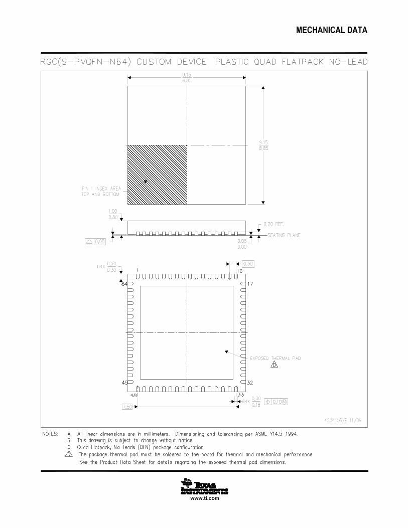
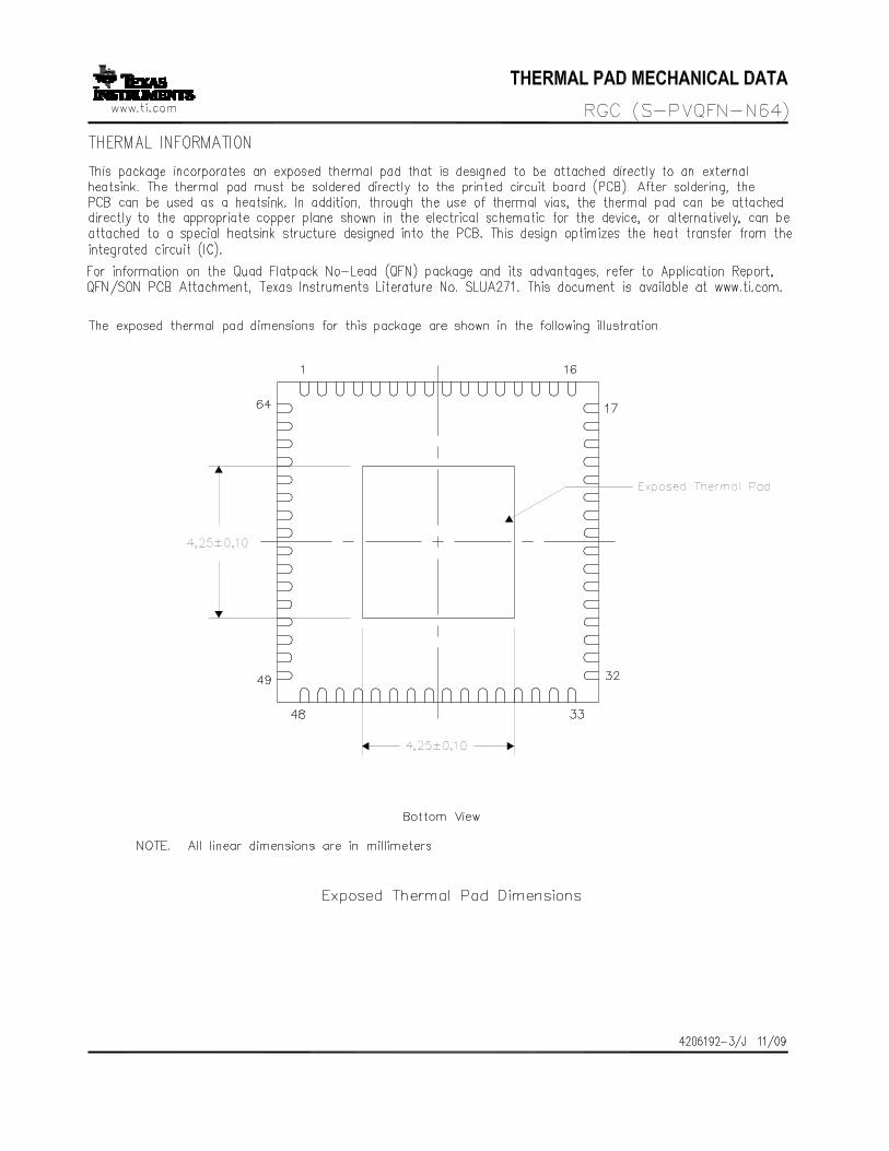
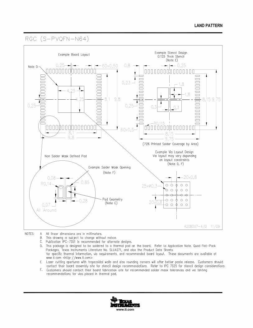
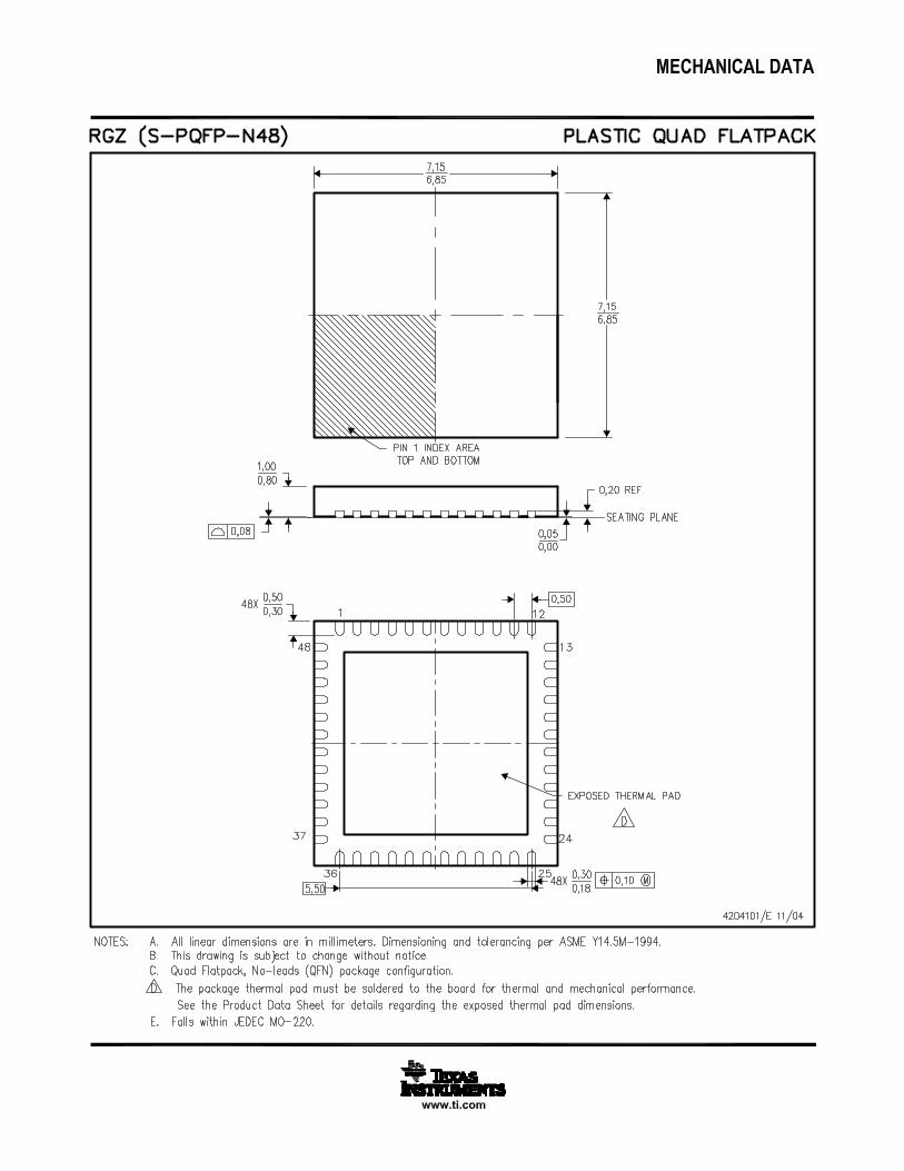
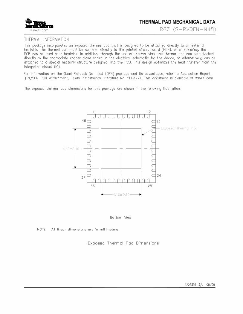
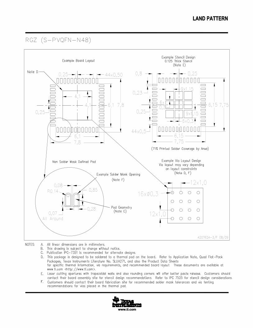
IMPORTANT NOTICETexas Instruments Incorporated and its subsidiaries (TI) reserve the right to make corrections, modifications, enhancements, improvements,and other changes to its products and services at any time and to discontinue any product or service without notice. Customers shouldobtain the latest relevant information before placing orders and should verify that such information is current and complete. All products aresold subject to TI’s terms and conditions of sale supplied at the time of order acknowledgment.TI warrants performance of its hardware products to the specifications applicable at the time of sale in accordance with TI’s standardwarranty. Testing and other quality control techniques are used to the extent TI deems necessary to support this warranty. Except wheremandated by government requirements, testing of all parameters of each product is not necessarily performed.TI assumes no liability for applications assistance or customer product design. Customers are responsible for their products andapplications using TI components. To minimize the risks associated with customer products and applications, customers should provideadequate design and operating safeguards.TI does not warrant or represent that any license, either express or implied, is granted under any TI patent right, copyright, mask work right,or other TI intellectual property right relating to any combination, machine, or process in which TI products or services are used. Informationpublished by TI regarding third-party products or services does not constitute a license from TI to use such products or services or awarranty or endorsement thereof. Use of such information may require a license from a third party under the patents or other intellectualproperty of the third party, or a license from TI under the patents or other intellectual property of TI.Reproduction of TI information in TI data books or data sheets is permissible only if reproduction is without alteration and is accompaniedby all associated warranties, conditions, limitations, and notices. Reproduction of this information with alteration is an unfair and deceptivebusiness practice. TI is not responsible or liable for such altered documentation. Information of third parties may be subject to additionalrestrictions.Resale of TI products or services with statements different from or beyond the parameters stated by TI for that product or service voids allexpress and any implied warranties for the associated TI product or service and is an unfair and deceptive business practice. TI is notresponsible or liable for any such statements.TI products are not authorized for use in safety-critical applications (such as life support) where a failure of the TI product would reasonablybe expected to cause severe personal injury or death, unless officers of the parties have executed an agreement specifically governingsuch use. Buyers represent that they have all necessary expertise in the safety and regulatory ramifications of their applications, andacknowledge and agree that they are solely responsible for all legal, regulatory and safety-related requirements concerning their productsand any use of TI products in such safety-critical applications, notwithstanding any applications-related information or support that may beprovided by TI. Further, Buyers must fully indemnify TI and its representatives against any damages arising out of the use of TI products insuch safety-critical applications.TI products are neither designed nor intended for use in military/aerospace applications or environments unless the TI products arespecifically designated by TI as military-grade or "enhanced plastic." Only products designated by TI as military-grade meet militaryspecifications. Buyers acknowledge and agree that any such use of TI products which TI has not designated as military-grade is solely atthe Buyer's risk, and that they are solely responsible for compliance with all legal and regulatory requirements in connection with such use.TI products are neither designed nor intended for use in automotive applications or environments unless the specific TI products aredesignated by TI as compliant with ISO/TS 16949 requirements. Buyers acknowledge and agree that, if they use any non-designatedproducts in automotive applications, TI will not be responsible for any failure to meet such requirements.Following are URLs where you can obtain information on other Texas Instruments products and application solutions:Products ApplicationsAmplifiers amplifier.ti.com Audio www.ti.com/audioData Converters dataconverter.ti.com Automotive www.ti.com/automotiveDLP® Products www.dlp.com Broadband www.ti.com/broadbandDSP dsp.ti.com Digital Control www.ti.com/digitalcontrolClocks and Timers www.ti.com/clocks Medical www.ti.com/medicalInterface interface.ti.com Military www.ti.com/militaryLogic logic.ti.com Optical Networking www.ti.com/opticalnetworkPower Mgmt power.ti.com Security www.ti.com/securityMicrocontrollers microcontroller.ti.com Telephony www.ti.com/telephonyRFID www.ti-rfid.com Video & Imaging www.ti.com/videoRF/IF and ZigBee® Solutions www.ti.com/lprf Wireless www.ti.com/wireless
Mailing Address: Texas Instruments, Post Office Box 655303, Dallas, Texas 75265Copyright © 2009, Texas Instruments Incorporated