c.braggio 1 ,g.bressi 2 ,m.boscardin 3 g.carugno 1 ,g.galeazzi 4 ,n.zorzi 3 1) infn sez. padova
DESCRIPTION
1 cm Thick Silicon(Ge)Detectors at Liquid Helium Temperature From Surface to Volume (Neutrino Physics). C.Braggio 1 ,G.Bressi 2 ,M.Boscardin 3 G.Carugno 1 ,G.Galeazzi 4 ,N.Zorzi 3 1) INFN Sez. Padova 2) INFN Sez. Pavia , 3) IRST-ITC Trento 4) INFN Lab.Naz.Legnaro. Freeze out Effect. - PowerPoint PPT PresentationTRANSCRIPT
1 cm Thick Silicon(Ge)Detectorsat Liquid Helium Temperature
From Surface to Volume(Neutrino Physics)
C.Braggio1,G.Bressi2,M.Boscardin3
G.Carugno1,G.Galeazzi4,N.Zorzi3
1) INFN Sez. Padova
2) INFN Sez. Pavia , 3) IRST-ITC Trento
4) INFN Lab.Naz.Legnaro

1.Large Drifting Distances:Requirements
Freeze out Effect
Charge Trapping vs Si Purity
Mobility and Mean free path
2.Silicon Processing Stages
3.Experimental Set-Up
4.Results:
I-V ; C-V Characteristics
Charge Collection Efficiency vs V bias
Collection Efficiency vs Si Purity
5.Conclusions

Freeze-out Effect at Low Temperature
Ec-Ed = 10 meV , Ea – Ev = 30 meV
E KT@4 Kelvin = 0,3 meV
At T 10 kelvin Silicon is Intrinsically depleted
BENEFITS:No leakage current
Low Bias Voltage
But not enough
Cap. Detector = Geometrical Cap.

Charge Collection + Trapping at Low Temperature
Cascade Capture Model Developed by Pitaevskii Review Paper from Abakumov Sov.Phy.Sem.1978
2 Type of competiting processes:
a) Scattering Cross Section from Coulomb center
b) S.C.S from “forming dipoles”
For High Purity Material (less 10^14 imp/cm3) process b is dominating
b) Type Cross Section is proportional to ( Nd,a)3/4
To Decrease Dipoles SCS We Need High Purity Silicon
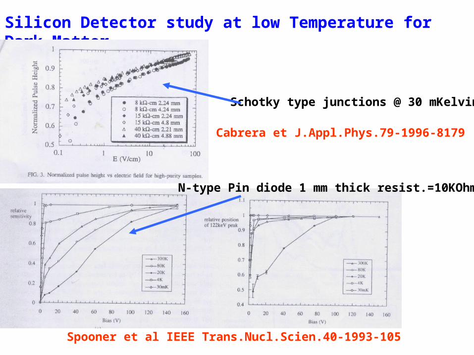
Silicon Detector study at low Temperature for Dark Matter
Schotky type junctions @ 30 mKelvin
N-type Pin diode 1 mm thick resist.=10KOhmcm
Cabrera et J.Appl.Phys.79-1996-8179
Spooner et al IEEE Trans.Nucl.Scien.40-1993-105

Mobility and Mean Free Path
At LHe Temp.mobility increases almost 3 O.M. respect to R.T.
Electron mean free path increases at Low Temp.
q E(V/cm) l = E ion (eV)
l = electron mean free path l = vsat. * Tau
Tau = mobility * mass / e
Mobility increases more than a factor 100
E avalanche from 10^5 to 10^3 V/cm
4 K 300 K

Silicon Processing Stages
Topsil / Wacker Ingot
Cutting Polishing Siliciumbearbeitung
IRST Schotky-PIN Diode

Experimental Set-Up
20 Lt LHe Dewar with LN2 Shielding
Silicon detector chamberFilled up with 2 mbar He GasTo attain good thermalization
Liq. Helium Evaporation Rate:1,3 Liq.Liter/hour

1E-1
1E+0
1E+1
1E+2
0 100 200 300 400 500 600 700Vrev [V]
Igr
[mA
]
reverse
forward
CRIO6 W1
1E+0
1E+1
1E+2
1E+3
1E+4
0 100 200 300 400 500 600 700|Vsub| [V]
Idio
de
[µ
A/c
m2]
reverse
forward
CRIO6 W1
Preliminar meas on test diodes and single PAD diodes
diode current density
1st guard-ring current
diode area:31cm2
diameter: 6.28cm
diode1st ring
1st ring2nd ring
P-Type Silicon PiN diode
Topsil material 40 KOhm*cm RT

Capacitance + Leakage Current
C and I vs Vbias measurements for 3 cm diam.
Capacity is costant vs Vbias at 4 Kelvin C =9,5 pF =Geom. Cap.
At 77 K C doesn’t saturate @120V C = 30 pF
Detector Leakage Current 1 pA/cm2 at 100V

Cold Electronic Chain
Si Detector at 4,7 Kelvin
Charge Amplifier at 120 K
To Silena Shaping Amplifier + EGG MCA
Electronic Noise = 1,9 KeV
FWHM (Right side) 60 Kev =4,2 KeV
60 KeV X Rays Spectrum
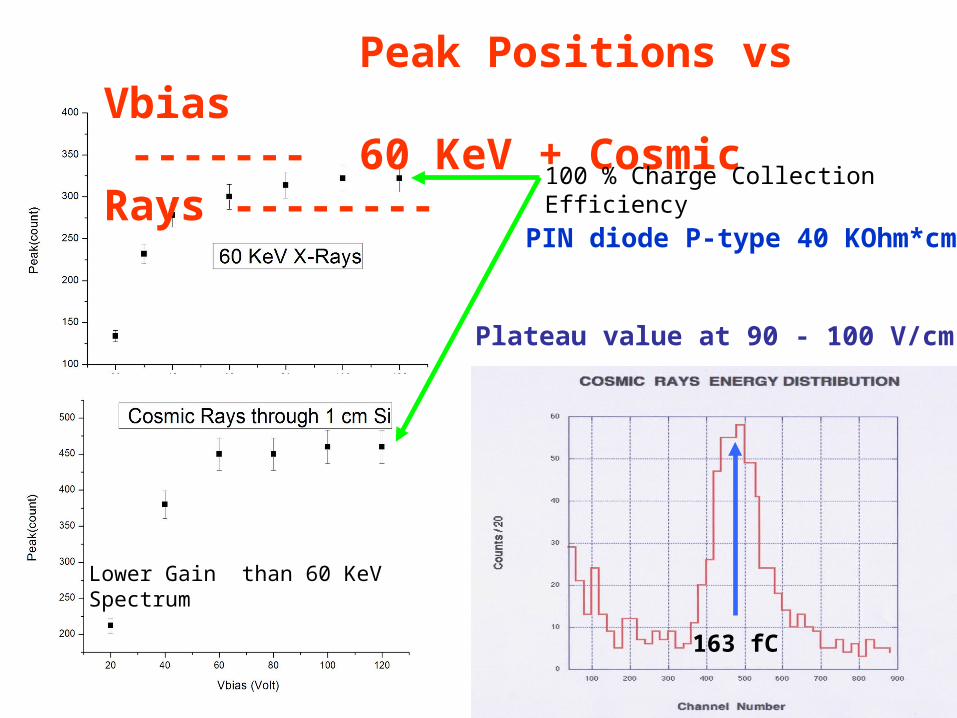
Peak Positions vs Vbias ------- 60 KeV + Cosmic Rays --------
100 % Charge Collection Efficiency
Plateau value at 90 - 100 V/cm
Lower Gain than 60 KeV Spectrum
PIN diode P-type 40 KOhm*cm
163 fC

Collection efficiency vs Purity
E (V/cm) @ 100% charge coll.eff. VS Resistivity (KOhm*cm @ RT)
a) 1000 6,8 n - type Wacker
b) 125 12 n – type Wacker
c) 90 40 p – type Top-Sil
Charge Collection Efficiency Depends Critically from Purity Sample
a) Braggio et al NIMA 568 (2006) 412b) Braggio et al NIMA accepted for pub.c) Braggio et this work

Home Made Germanium Schotky Barrier Detector
Co57 Gamma Source
Vbias = 25 Volt
Germanium purity 2 OfM Better than Silicon
1 Cm thick 3 cm Diam.
Germanium detector cost 50 times Lower than same planar device
Energy Resolution comparable With a standard Germanium
Cleaning procedure and electrode evaporation made in our lab.
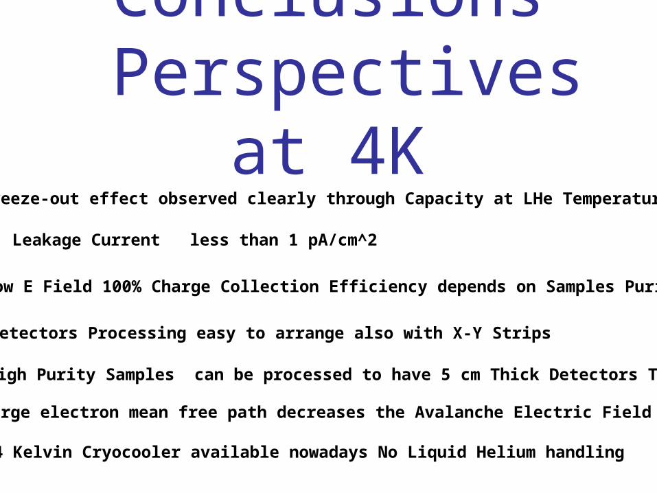
Conclusions Perspectives at 4K
1) Freeze-out effect observed clearly through Capacity at LHe Temperature
2) Leakage Current less than 1 pA/cm^2
3) Low E Field 100% Charge Collection Efficiency depends on Samples Purity
4) Detectors Processing easy to arrange also with X-Y Strips
5) High Purity Samples can be processed to have 5 cm Thick Detectors TPC
6) Large electron mean free path decreases the Avalanche Electric Field
7) 4 Kelvin Cryocooler available nowadays No Liquid Helium handling