cbc3 front end design progress - imperial college londondmray/systems_talks/2015/cbc3... · cbc3...
TRANSCRIPT

CBC3 front end design progress
11
systems meeting, 4th June, 2015.
Mark Raymond

CBC3 front end specs, requirements and simulation constraints
simulation (design) constraintsVDDA = 1V minimum operation
VDDA provided by LDOoperating temperature ~0 deg. C
simulate performance @ -20 and +30process corners
sensor constraintsn-in-p (electrons)
can scrap dual polarity requirement (helps with VDDAmin = 1.0V)AC coupled
no need to source leakage current (also helps with VDDAmin = 1.0V)5 cm length
2
5 cm lengthCtot ~ 7.5 pF (Cis~2.5pF, Cbp~2.5pF)
8 cm lengthprovision to increase input FET current to cope with
performance contraintspulse shape
peaking time <20nsec, pulse return to baseline within 50 nsecoverload recovery
normal response resumed 2.5 usec following 4pC hip signalnoise
target ENC < 1000e

CBC2 issues to address (in CBC3)
• leakage current in pipeline at low ionizing doseshttp://www.hep.ph.ic.ac.uk/~dmray/CBC_documentation/Phase_2_TID_Davide_Nov_14.pdf
enclosed NMOS devices now implemented
• I2C register SEU immunity could be betterhttp://www.hep.ph.ic.ac.uk/~dmray/CBC_documentation/Phase_2_SEU_Kirika_Nov_14.pdf
now plan to use Whitaker cells for registers
• CM effect in electrons polarity modeshows up when threshold low and many channels firingtraced to postamp feedback FET biasing
http://www.hep.ph.ic.ac.uk/~dmray/systems_talks/2015/CBC2_CM_systems_Jan2015.pdf
a new method for biasing the feedback FET is required
3
a new method for biasing the feedback FET is required
• so-called “shadow effect”when signal injected into many channels, other channels fire, but ~50ns latertraced to coupling through preamp cascode bias
http://www.hep.ph.ic.ac.uk/~dmray/systems_talks/2015/CBC2_shadow_effect_Apr_2015.pdf
preamp cascode now individually biased using regulated cascode circuit

CBC3 Preamp modifications
design changes reported last time
increase I/P device bias transistor width (last time)(allows to run more current if necessary)
scrap T-network for holes polarity
reduce Rf to 100k(needed for reduced pulse peaking time)
4/1
CBC2 preamp
4
400/0.36
25/0.25
100k
IPSF
25/0.5
10/160/1 IPRE2IPRE1
Cfp
100f electrons
10/1
4/1
10/0.25
25uA 10uAregulated cascode circuit
bigger open loop gain
self biasing so no need forcommon global bias
(fix for “shadow effect”)
small power penalty

CBC2 Postamp
VPLUS
IPA
Cc
1p
Ipaos1 Ipaos210/0.5 10/1 10/1
5/0.25
5/0.2525/0.5
Ccomp
100f
20k25/0.25 25/0.25
10/.5
IPA
51uA
IPA
25uA VPLUS
10/1 10/1
feedback
network
postamp bias (1 per chip)
80f
100p
no reason to change the op-amp itself
the feedback network is another matter

+
-
VPLUS
1p
1p
80f
h h
h
ee
CBC2 postamp feedback
1/5
1/5postamp
feedback
evidence that disturbance on VPAFB(when many comparators fire)couples to VPLUS in electrons mode*
& VPLUS also feeds opamp non-inverting input
VPLUS
h
e
1MVPAFB
1/5
feedback
network
(1 per chan.)
1 per chip
VDDA
VDDA
200k
~4uAvoltage bias
(like VPC and
VPLUS)
1 per chip
* http://www.hep.ph.ic.ac.uk/~dmray/systems_talks/2015/CBC2_CM_systems_Jan2015.pdf

+
-
VPLUS1p
80f
CBC3 postamp feedback
1/5
VPAFB
(global signal)
VPLUS2
current
mirror
simplify to 1 feedback FETfor electrons polarity signal
electrons
extra precaution: VPLUS2 = copy of VPLUS, independently generated => no possibility of cross-coupling
between bias network and postamp opamp +ve input
would like to use resistor ladder DAC approach for VPLUS and VPLUS2
100p
R
1/51/5
beta multiplier circuit used to
reliably generate small current
(~10’s nA) in mirror transistor
(see backup for more info)10/1 40/1
1 per chip

VPLUS2
100p
1/51/5external RST
(active high)
aux. I2C RST(from an I2Cregister - low
for normaloperation)
VPAFB
beta multiplier plus start-up and adjustable R
10/1
10/1 40/1
2/.2 2/.2 2/.2 2/.2s1 s2 s3 s4
8
4M 2M 1M 0.5M
all NMOS enclosed (leakage currents would mess things up)
exclusive OR of RST (startup) lines ensures we can’t have a disaster (i.e. get polarity wrong and getstuck in permanent reset!!)

beta multiplier performance vs. adjustable R
cycling through all possible resistorswitch combinations
all process cornersT=-20 & +30VPLUS=0.45, 0.5, 0.55
strongest effect is Tlower family -20upper family +30
curr
ent in
mirro
r tr
ansis
tor
maste
r [A
]
9
allswitches
on
allswitches
off
curr
ent in
mirro
r tr
ansis
tor
maste
r [A
]

+
-
VPLUS
1p80f
postamp modifications finished
1/5
now look at effect of modifyingswitch settings on pulse shape
s4 s3 s2 s1 = 0000 to 1111
VPLUS2
10
VPAFB
VPLUS2
100p
4M
1/51/5
2M 1M 0.5M
10/1
10/1 40/1
2/.2 2/.2 2/.2 2/.2s1 s2 s3 s4

normal behaviour (1 to 5 mips)
2.5 fC to 12.5 fC, 2.5 fC steps(one to five mips)
all process corners, T = -20 & +30
least significant postamp fb currentsetting - 0001
Cin = 8p, Cstray = 2p, IPRE1 = 30IPRE2 = 25, IPSF=25, IPA=20
preamp feedback 100k
11
VDDA = 1V
10 nsec
1 nsec
sensor current pulse model

normal behaviour (1 to 5 mips)
2.5 fC to 12.5 fC, 2.5 fC steps(one to five mips)
all process corners, T = -20 & +30
least significant postamp fb currentsetting - 0010
Cin = 8p, Cstray = 2p, IPRE1 = 30IPRE2 = 25, IPSF=25, IPA=20
preamp feedback 100k
12
VDDA = 1V

normal behaviour (1 to 5 mips)
2.5 fC to 12.5 fC, 2.5 fC steps(one to five mips)
all process corners, T = -20 & +30
least significant postamp fb currentsetting - 0100
Cin = 8p, Cstray = 2p, IPRE1 = 30IPRE2 = 25, IPSF=25, IPA=20
preamp feedback 100k
13
VDDA = 1V

normal behaviour (1 to 5 mips)
2.5 fC to 12.5 fC, 2.5 fC steps(one to five mips)
all process corners, T = -20 & +30
least significant postamp fb currentsetting - 1000
Cin = 8p, Cstray = 2p, IPRE1 = 30IPRE2 = 25, IPSF=25, IPA=20
preamp feedback 100k
14
VDDA = 1V

normal behaviour (1 to 5 mips)
2.5 fC to 12.5 fC, 2.5 fC steps(one to five mips)
all process corners, T = -20 & +30
least significant postamp fb currentsetting - 1111
Cin = 8p, Cstray = 2p, IPRE1 = 30IPRE2 = 25, IPSF=25, IPA=20
preamp feedback 100k
15
VDDA = 1V
conclusion
pulse shape robust to process and T
some tunability of postamp pulseshape achievable using feedbackFET bias

2.5 fC signal (1 mip)
typical process params, T = 0 deg.
postamp fb current setting - 1000
Cin = 8p, Cstray = 2p, IPRE1 = 30IPRE2 = 25, IPSF=25, IPA=20
IPA 10u -> 30u , 5u steps
VPLUS = VDDA/2
effect of IPA
16
conclusion
varying IPA gives extra handle onpulse shape tunability

noise performance vs C
1200
1000
800
600
400
EN
C [ele
ctr
ons]
dependence on Cadded for fixed 200uA current in I/P FET
total front end power ~350uW (preamp+postamp+comp)T = +30
Cadded = 0 to 12pF, 2pF steps
all process cornersT = +30T = -20
17
400
200
0121086420
EN
C [ele
ctr
ons]
Cadded [pF]
(5cm x 1.5pF/cm) + Cstray~2pF
T = -20
=> ~1000e achievable for target power consumption

noise vs power
dependence on power for fixed valuesof Cadded
varying current in input FET(PFET = IFET x 1.2)
choose 2 input capacitance values
simulations for typical process paramsonly, T = +30 and -20
PFET = 150 to 330 uW Cadded = 10 pF
PFET = 260 to 680 uW Cadded = 15 pF
T = +30
T = -20
T = +30
T = -20
18
1400
1200
1000
800
600
400
200
07006005004003002001000
closed symbols Cadded = 10 pF total (2 stray + 8 sensor)<1000e for ~250uW in I/P FET for T~0
open symbols Cadded = 15 pF total (2 stray + 13 sensor)<1000e for ~600uW in I/P FET for T~0
must add ~100uW for rest of front end+ digital
EN
C [ele
ctr
ons]
T = +30T = -20
input FET power only [uW]

front end conclusions
preamp/postamp pre-layout design modifications now well advanced
core amplifier circuits mostly left alone
specifications met
design robust to temperature and process variations
minimal pulse shape variations
CBC2 shortcomings addressed (preamp cascode and postamp feedback)
19
CBC2 shortcomings addressed (preamp cascode and postamp feedback)
comparator still needs looking at to achieve neutral current consumption

now look at hips behaviour - M.Huhtinen simulations
Differential Energy spectrum: Probability/incident pion of depositing energy E in 300µm Si layer
10-3
10-4
10-5
10-4
10-5
10-6
Integral spectrum: total prob. of pion depositing energy > E X5
CMS
spec. based on what is achievable
channel receiving 4 pC signal should be sensitive to normal signals after 2.5 usec
10-6
10-7
1 MeV 10 MeV 100 MeV0.1 MeV
10
10-7
1 MeV 10 MeV 100 MeV0.1 MeV
E
1 MIP (300µ Si) = .090 MeV 100 MeV = 1111 MIP
E
4.4 pC440 fC44 fC

hips behavioursingle channel response
4 pC injected at t=100ns, 2.5 fC injected at t=2.5us
preamp input
preamp output
preamp can’t “swallow” 4 pC=> voltage builds up at input and discharges away
through feedback resistance
preamp output saturates until charge has decayedaway, then returns quickly to baseline
21
postamp input
postamp output
preamp output injects signal into postamp inputvia 1pF coupling capacitance. +ve signal dischargesslowly (postamp feedback in high resistance region)-ve signal discharges quickly (postamp feedbackin low resistance region)
postamp output initially saturates -vewhen preamp output recovers postamp outputinitially saturates +ve, recovers quickly but overshootsthen recovers more slowly to baseline
back to normal sensitivity within 2.5 usec

hips behaviour - single channel response
22
single channel postamp output response
4 pC injected at t=100ns, 2.5 fC injected at t=2.5usall process corners, T=- 20 and +30
longest recovery for slow N & slow P corner at T= -20
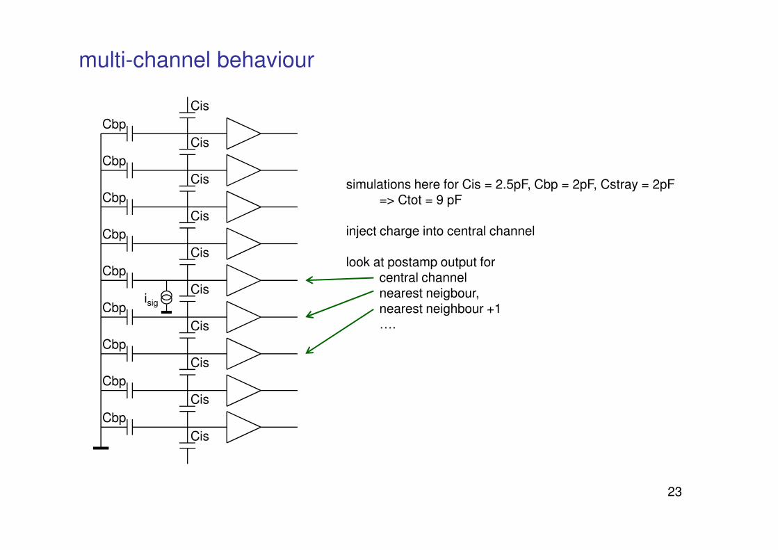
multi-channel behaviour
Cis
Cis
Cis
Cis
Cis
Cbp
Cbp
Cbp
Cbp
Cbp
simulations here for Cis = 2.5pF, Cbp = 2pF, Cstray = 2pF=> Ctot = 9 pF
inject charge into central channel
look at postamp output for central channel
23
Cis
Cis
Cis
Cis
Cis
Cbp
Cbp
Cbp
Cbp
Cbp
central channelnearest neigbour,nearest neighbour +1….
isig

interstrip crosstalk
nearestneighbour
nn+1
2.5 fC charge injectedT=-20/+30all cornersnominal biases
nearest neighbour peakcrosstalk ~ 5 %
24
centre channel

hipscentre channel
nearest neighbour
nn+1
nn+2
40fC injected on centre channel at t = 100 nsec(nominal bias conditions, typical process params)
2.5 fC injected on all channels at t = 2.5 usec
(5 mips = ~13 fC)
25
nn+3
nn+4
nn+5

hipscentre channel
nearest neighbour
nn+1
nn+2
100fC injected on centre channel at t = 100 nsec
2.5 fC injected on all channels at t = 2.5 usec
26
nn+3
nn+4
nn+5

hipscentre channel
nearest neighbour
nn+1
nn+2
400fC injected on centre channel at t = 100 nsec
2.5 fC injected on all channels at t = 2.5 usec
27
nn+3
nn+4
nn+5

hipscentre channel
nearest neighbour
nn+1
nn+2
1pC injected on centre channel at t = 100 nsec
2.5 fC injected on all channels at t =2.6 usec
all channels recovered by ~1.5 usec
28
nn+3
nn+4
nn+5

hipscentre channel
nearest neighbour
nn+1
nn+2
4pC injected on centre channel at t = 100 nsec
2.5 fC injected on all channels at t = 2.6 usec
all channels recovered within ~2 usec
centre channel recovers beforenn, nn+1, ~nn+2
significant deadtime for centre chan.,nn, nn+1, nn+2
29
nn+3
nn+4
nn+5
nn+3 etc. ~ok

hips worst case
4pC injected on centre channelat t = 100 nsec
2.5 fC injected on all channelsat t = 2.5 usec
look at worst channel nn+1
T=-20, +30, all corners
all channels recovered by 2.5 usec irrespective of
30
2.5 usec irrespective ofsim. conditions

hips and multi-channel simulations summary
interchannel crosstalk at ~5% level for normal signals
hips effects confined to central hit strip and some neighbours
number of neighbours depends on signal size
worst case 7 channels for 4 pC
~ 3-4 channels for 400 fC
~ negligible effect up to ~40 fC
31

BACKUP
32
BACKUP

100p
R
1/51/5
VPAFB
beta multiplier “explained”
40/110/1
β = µCOX(W/L) [proportional to W]
Iref Iref
33
upper mirror forces same current (Iref) to flow in both lower transistors
ok if VGS(left) > VGS(right), which can be achieved by making right NMOS wider than left by multiplier factor K (40/10)
in weak inversion Iref = nUTlnK (UT = kT/q)R
=> R ~ 5M for Iref = 10nA (n ~ 1.4, K=4, UT ~ 25 mV)
see CMOS Circuit Design, Layout and Simulation (3rd ed.) R. Jacob Baker, chapter 20(particularly page 635 for weak inversion design)

preamp input preamp output
why is nearest neighbour deadtime worse than centre channel?
voltage on preampinput of nn goesslightly positive dueto coupling throughCis
causes preampoutput to go low- results in risingedge at end ofrecovery time
centre channelnearest neighbour
34
postamp inputpostamp output
which in turncauses postampinput to gopositive. postampfeedback FET isin high resistanceregion
high resistancefeedback meanspostamp takeslonger to recover

+
-
VPLUS
1pF
80f
1/5
VPAFB
postamp feedback characteristics reminder
ISD
VPLUS
negative going signal(high resistance quadrant)
positive going overshoot(low resistance quadrant)
electrons mode signal
-ve going signal regionsource at input side of
increasing |VGS|
bias to FB transistor
(decreasing VPAFB)
ISD
VDS
VPAFB
VPAFB
source at input side ofpostampVGS ~ constantonly VDS varies
+ve going overshoot regionsource swaps to output sideVGS increases as postampoutput overshoot increases

36

CBC2 Preamp
VPC
400/0.36
25/0.25
200k
118 sq.
h h
ee
25/0.5
10/120/1 IPRE2IPRE1
Cfp
100f
s
s
2/0.2
6/0.2
switch
All NMOS enclosed
(also triple well)
holesCc
1p
60k
35 sq
92k
54 sq
115k
68 sq
IPSF
h h
10/1
IPRE2
51uA
IPRE2 IPSF
51uA
IPSF10/1
VPC
switch
implementation
(NMOS enclosed)
100p
10/1
IPRE1
128uA
IPRE1
10/1
100p
100p

CBC2 Postamp
VPLUS
IPA
Cc
1p
Ipaos1 Ipaos210/0.5 10/1 10/1
5/0.25
5/0.2525/0.5
Ccomp
100f
20k
(yes!-20k)
25/0.25 25/0.25
10/.5
IPA
51uA
IPA
25uA VPLUS
All NMOS enclosed
(also triple well)
10/1 10/1
feedback
network
postamp bias (1 per chip)
80f
100p

CBC2 comparator
VCTHIN
10/0.18 10/0.18
1/0.5 1/0.5
1/0.5
0.16/
0.12
O/P
0.48/
0.12
0.16/
0.12
0.16/
0.12
16/1
8/18uA
4uA
1.1 V analogue 1.2 V digital
analogue and digital
domains split here
ICOMP
Nop
ICOMP
Nop
Ihyst
.16/0.12
.16/0.12
5/.5
8/1
16/1
4uA
1 per chip
ICOMP
25uA
ICOMP
ICOMP ICOMPIhyst
Ihyst
h0 h1 h2 h3
1.1 V
1000k 500k 250k 125k 5000k
gnd
gnd
50/.5
5/.55/.55/.55/.5
100p

CBC2 Postamp Output
Offset Adjust10/1
0.6/0.6 0.6/0.6 0.6/0.6 0.6/0.6 VPLUS
s1
s1b
2/0.2
M=1 M=2 M=4 M=64 M=128
s2
s2b
2/0.2s4
s4b
2/0.2s64
s64b
2/0.2s128
s128b
2/0.2
IPAOSs1, s1b, s2, s2b , … s128, s128b
provided by 8 bit register / channel
2/0.2 2/0.2 2/0.2 2/0.2 2/0.2
12.5uA
20/1
IPAOS
25uA
IPAOS
10/1 Ipaos1
All NMOS enclosed
(also triple well)
10/1 25/1
VPLUS10/1
10/1 Ipaos2
10/1 25/1
VPLUS10/1
master bias (1 / chip)
0-30uA 30-0uA
100p

+
-
VPLUS
1p
1p
80f
h h
ee
CBC2 postamp feedback
s
s
2/0.2
6/0.2
switch
implementation
(NMOS enclosed)
1/5
1/5postamp
VPLUS
1p
h
e
1MVPAFB
1/5
postamp
feedback
network
(1 per chan.)
1 per chip
VDDA
VDDA
200k
~4uAvoltage bias
(like VPC and
VPLUS)
1 per chip