cb7210.2 data sheet - bentech taiwanmccdaq.bentech-taiwan.com/gpib/cb7210.2.pdf · vhdl source...
TRANSCRIPT

µPD7210 vs. CB7210.2
Features
Meets IEEE Standard 488.2-1992* SH1, source handshake AH1, acceptor handshake T5 or TE5, talker or extended talker L3 or LE3, listener or extended listener SR1, service request RL1, remote local PP1 or PP2, parallel poll, remote or local configuration DC1, device clear DT1, device trigger VHDL Source Available C1-C5, controller, all functions
The CB7210.2 is designed entirely in VHDL code and implemented as the state machines defined in the IEEE-488.2 specification, and the NEC µPD7210 data book. The CB7210.2 includes state machines which implement advanced functions found on the TNT488.2 GPIB controller from National Instruments. The VHDL code is available to manufacturers and OEM's designing systems and chips for GPIB instrumentation, control and analysis. Licenses are available for as little as fifty cents per instance of use.
Programmable data transfer rate 16 registers, 8 read/8 write 2 address registers
Detection of MTA, MLA, MSA (my talk/my listen/my secondary addresses) 2 device addresses
EOS Message Automatic Detection Command (IEEE Standard 488-78) automatic processing and undefined command read capability DMA capability Programmable bus transceiver I/O specification (works with Texas Instruments/Motorola/Intel-compatible High Speed State Machine Bus/FIFO
Manager 1 MHz to 20 MHz* clock range Can monitor all bus control lines* An advanced state machine designed to handle bus transfers
and a FIFO specifically for the CB7210.2 is available for the ISA, PCMCIA and PCI bus. You can integrate the ASIC equations into your own design.
Supports T1 delays of 2000, 500, 350 ns* +5V single power supply CMOS technology 8080/85/86 compatible
Simply the Best GPIB Chip in the WORLD Available in 40 Pin DIP and 44 Pin TQFP* packages Adds 488.2 features to NEC µPD7210 design* The CB7210.2 is the best GPIB interface chip in the world.
With an open design, unparalleled software support, advanced support circuitry, low cost and backed by Measurement Computing Corporation, the CB7210.2 is the new standard in GPIB components.
*Items marked with an asterisk and shown in red are new features that are not supported by the NEC µPD7210.
The CB7210.2 is the new standard GPIB controller chip replacing the NEC µPD7210. Like many OEMs facing the eventual phasing out of the NMOS NEC µPD7210, Measurement Computing Corporation (MCC) needed a replacement, and needed it to embrace the latest technology, to preserve legacy code and circuitry, and to be available at a great price. So we designed one from the ground up.
IEEE-488.2 (GPIB) Compatibility The CB7210.2 adheres to ANSI/IEEE Standard 488-1978, and the update to the IEEE-488.2 specification. The IEEE-488 bus or GPIB (General Purpose Interface Bus) is a standard for instrumentation communication and control for instruments from manufacturers the world over. Other vendors have introduced GPIB chips that are either
outdated, such as the IOTech version which only supports 488.1 commands, or are restricted to Talker/Listener, such as the TNT488.2 chip from National Instruments. MCC's CB7210.2 is priced as low as $8.00 in quantity, available in unrestricted Controller/Talker/Listener with all enhanced registers functioning, preserves legacy code in either package and preserves legacy circuitry in the 40-pin package.
Free Samples Free samples of the CB7210.2 are available to OEMs or to anyone who owns any equipment with a socket for an NEC µPD7210 and wants to upgrade to the latest technology.
Page 1 of 16

µPD7210 vs. CB7210.2
Availability The CB7210.2 is a high performance extended version of the NEC µPD7210 GPIB controller chip. It is 100% software and hardware compatible with the NEC chip and can be used as a drop in replacement in existing designs. The CB7210.2 offers a number of significant enhancements. For new designs, the chip provides both higher performance and additional features.
The lack of a good chip source drove us to develop the CB7210.2. We are not like most big chip suppliers that let delivery on a chip stretch out to 12-16 weeks. In fact, we are our biggest customer. Without an adequate supply of chips, we can't ship our very successful GPIB board product line. You can be sure that we'll have the components when you need them. And since we have such a large investment in boards that use the chip, you can be sure that any chip upgrade or revision will not jeopardize 100% compatibility with previous versions. We don't want to REV our boards any more than you do!
Higher Performance The maximum clock rate of the µPD7210 is 8 MHz. The CB7210.2 chip increases the maximum clock rate to 20 MHz. When running at identical clock rates, the CB7210.2 executes the GPIB handshaking protocol at faster rates, due to a more optimized design of the internal circuitry.
Low Price Those of you who know us from our highly successful board business know that Measurement Computing Corporation has built its business on providing quality products at extremely low prices. Look at the pricing of our board products and you'll see that we're serious about offering low prices. We're following this same low cost strategy on our chip products. Our goal is to never give you a reason to buy from anyone else. We offer premium quality products at rock bottom prices with quick delivery. Then we back the whole package up with exceptional service.
The CB7210.2 also supports a T1 delay of 350 ns (the minimum allowed by the IEEE 488 specification) in addition to the 500 ns and 2000 ns delays that are supported by the NEC µPD7210. These speed improvements allow straightforward hardware designs that can easily achieve the IEEE 488 specifications nominal maximum throughput of 1 MHz. With the CB7210.2 chip, the GPIB cable itself is the bottleneck. With a short cable, the CB7210.2 chip is capable of >1.5 MHz transfer speeds.
New Features New Packaging The CB7210.2 chip adds new features to the NEC
µPD7210 that are implemented via new "hidden" registers added to the µPD7210 register map. These features are invisible when running existing µPD7210 software, but can be accessed by any software written for the CB7210.2 chip. The new features include:
The µPD7210 is only available in a 40 pin DIP package, which is huge by today's standards. The CB7210.2 is available in a 44-pin, TQFP package that is small enough for use in PCMCIA cards, PC104 cards or in OEM applications where board real estate is at a premium. The TQFP package is also surface-mount compatible. Ability to monitor the state of all bus control lines.
Ability to monitor the internal state of all GPIB state machines. Bus/FIFO Manager Design Available Improved SRQ handling as specified by IEEE 488.2. Includes Request For Service (RSV) state machine and support of local messages "reqt" and "reqf".
We've even done some of the board design work for you. While designing our own board level products, we developed an advanced state machine designed to handle bus transfers and a FIFO specifically for the CB7210.2. These designs are available for sale on the ISA, PCMCIA and PCI bus. Please call us at (508) 946-5100 for further details regarding our high-speed GPIB support designs.
Supports 350 ns T1 delay in addition to the 500 ns and 2000 ns T1 delays supported by the NEC µPD7210.
CMOS Technology The original µPDP7210 was built in NMOS technology. This technology was state-of-the-art 20 years ago when the chip was released, but is outdated by today's standards. Today's CMOS is faster, consumes less power, and has equivalent drive capability with higher input impedances. These advantages, combined with the high circuit densities available, allow the new chip to offer higher performance and lower cost than the older µPDP7210.
Page 2 of 16

Pin identification and Configuration
Pin # PDIP TQFP
Signal name*
I/O Description
1 40 T/R1 O Transmit/Receive Control. Input/output control signal for the GPIB bus transceivers.
2 41 T/R2 O Transmit/Receive Control. The values of T/R2 and T/R3 are determined by the values of the Address Mode register bits TRM1, and TRM0.
3 42 CLK I
Clock. 1 MHz to 20 MHz reference clock for generating the state change prohibit times T1, T6, T7, T9 specified in IEEE Standard 488.2-1992.
4 43 RESET I Reset. Resets the CB7210.2 to an idle state when high (active high).
5 44 T/R3 O Transmit/Receive Control. See T/R2. 6 1 DRQ O DMA Request. Requests data transfer. Becomes
low on input of DMA acknowledge signal DACK. 7 2 DACK/ I DMA Acknowledge. (Active Low) Signal
connects the computer system data bus to the data register of the CB7210.2.
8 3 CS/ I Chip Select. (Active Low) Enables access to the register selected by RS0-RS2 (read or write operation).
9 4 RD/ I Read. (Active Low) Places contents of read register specified RS0-RS2 on D0-D7 (computer bus).
10 5 WR/ I Write. (Active Low) Writes data on D0-D7 into the write register specified by RS0-RS2.
11 7 INT O Interrupt Request. (Active High/Low) Becomes active due to any 1 of 13 internal interrupt conditions (unmasked). Active state software configurable. Active high on chip reset.
12-19 8-15 D0-D7 I/O Data Bus. 8-bit bidirectional data bus for interface to the computer system.
20 6, 17, 28, 39
GND Ground
21-23 18-20 RS0-RS2 I Register Select. These lines select one of eight read (write) registers during a read (write) operation.
24 21 IFC/ I/O Interface Clear. Control line used for clearing the interface functions.
25 22 REN/ I/O Remote Enable. Control line used to enable remote operation of the devices.
26 23 ATN/ I/O Attention. Control line which indicates whether data on DIO lines is an interface message or device dependent message.
27 24 SRQ/ I/O Service Request. Control line used to request service from the controller.
28-35 25-33 DIO1/-DIO8/
I/O Data Input/Output. 8-bit bi-directional bus for transfer of message.
36 34 DAV/ I/O Data Valid. Handshake line indicating that data on DIO lines is valid.
37 35 NRFD/ I/O Ready for Data. Handshake line indicating that device is ready for data.
38 36 NDAC/ I/O Data Accepted. Handshake line indicating completion of message reception.
39 37 EOI/ I/O End or Identity. Control line used to indicate the end of multiple byte transfer sequence or to execute a parallel polling in conjunction with ATN.
40 16, 38 VCC I/O +5 VDC * A "/" suffix following the signal name indicates that the signal is active low.
CB7210.2 – PDIP
1
2
3
4
5
6
7
8
9
10
11
12
13
14
15
16
17
18
19
20 21
22
23
24
25
26
27
28
29
30
31
32
33
34
35
36
37
38
39
40 V
RS2
RS1
RS0
IFC
REN
ATN
SRQ
DIO1
DIO2
DIO3
DIO4
DIO7
DAVNRFD
NDAC
EOI
DIO6
DIO5
DIO8
T/R1
T/R2
CLK
RESETT/R3
DRQ
DACK
INT
D0
D1
D2
D3
D4
D5
D6
D7
GND
CS
RD
WR
CB7210.2 – TQFP
DRQ
GND
INT D0
D1
D2
D3
GND
T/R3
RESETCLKT/R2
T/R1
GND+5
DAV
D4
D5
D6
D7
+5GNDRS0
RS1
RS2
DIO8
DIO7
DIO6
DIO5
DIO4
DIO3
DIO2
DIO1
SRQ
ATN
RENIFC
DACK CS
RD
WR
1 2 3 4 5 6 7 8 9 10
11
2324
25
2627
28
29303132
33
121314151617181920
212234
35
363738394041424344
NRFDNDACEOI
Page 3 of 16

Block Diagram
Data In
Command PassThrough
Byte Out
AddressMode
Address 0/1
End-of-String
InterruptMask 1/2
Interrupt Status 1/2
SerialPoll
ParallelPoll
Aux A/B/E
InternalCounter
AddressStatus
AuxiliaryCommandDecoder
MessageDecoder
InterfaceFunctions
SH1
AH1
T5/TE5
L3/LE3
SR1
RL1
PP1/PP2
DC1
DT1
C1
C2
C3
C4
C5
Read/WriteControl
RS -RS2 0
DRQ
RD
GPIB CONTROL
T/R -T/R3 1
D -D7 0
INT
CLOCK
RESET
DIO -DIO8 1
CS
WR
DACK
Bus State
InternalStates
Page 4 of 16
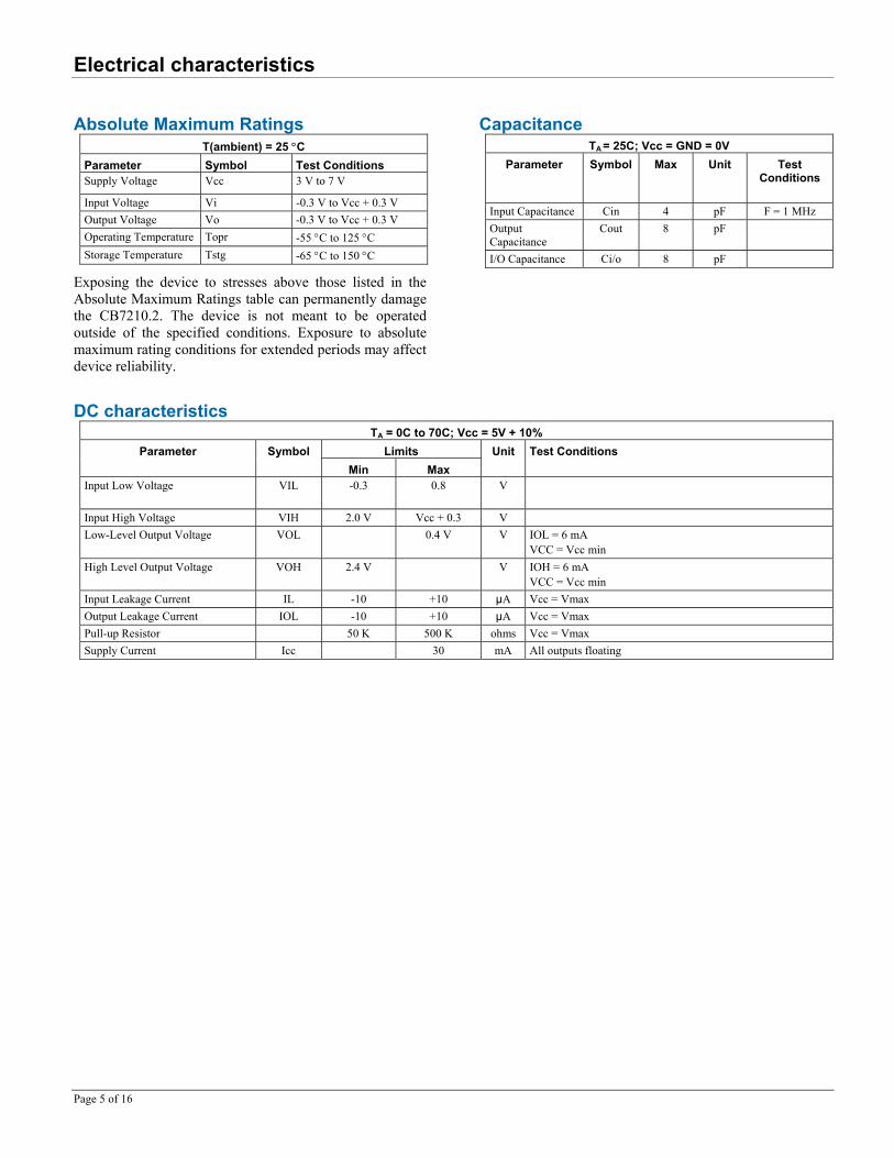
Electrical characteristics
Absolute Maximum Ratings T(ambient) = 25 °C
Parameter Symbol Test Conditions Supply Voltage Vcc 3 V to 7 V
Input Voltage Vi -0.3 V to Vcc + 0.3 V Output Voltage Vo -0.3 V to Vcc + 0.3 V Operating Temperature Topr -55 °C to 125 °C Storage Temperature Tstg -65 °C to 150 °C
Exposing the device to stresses above those listed in the Absolute Maximum Ratings table can permanently damage the CB7210.2. The device is not meant to be operated outside of the specified conditions. Exposure to absolute maximum rating conditions for extended periods may affect device reliability.
Capacitance TA = 25C; Vcc = GND = 0V
Parameter Symbol Max Unit Test Conditions
Input Capacitance Cin 4 pF F = 1 MHz Output Capacitance
Cout 8 pF
I/O Capacitance Ci/o 8 pF
DC characteristics TA = 0C to 70C; Vcc = 5V + 10%
Limits Parameter Symbol Min Max
Unit Test Conditions
Input Low Voltage VIL
-0.3 0.8 V
Input High Voltage VIH 2.0 V Vcc + 0.3 V Low-Level Output Voltage VOL 0.4 V
V IOL = 6 mA
VCC = Vcc min High Level Output Voltage VOH 2.4 V V IOH = 6 mA
VCC = Vcc min Input Leakage Current IL -10 +10 µA Vcc = Vmax Output Leakage Current IOL -10 +10 µA Vcc = Vmax Pull-up Resistor 50 K 500 K ohms Vcc = Vmax Supply Current Icc 30 mA All outputs floating
Page 5 of 16

Registers
Internal registers The CB7210.2 has 16 registers: 8 read and 8 write. The register names marked with an * and shown in gray table cells are not compatible with the NEC µPD7210.
Register Name Addressing Specifications RS2 RS1 RS0 WR/ RD/ CS/
Data In [OR] 0 0 0 1 0 0 D17 D16 D15 D14 D13 D12 D11 D10 Interrupt Status 1 [1R] 0 0 1 1 0 0 CPT APT DET END DEC ERR D0 D1 Interrupt Status 2 [2R] 0 1 0 1 0 0 INT SRQI LOK REM CO LOKC REMC ADSC *Serial Poll Status [3R]
0 1 1 1 0 0 S8 PEND S6 S5 S4 S3 S2 S1
*Revision [3R] 0 1 1 1 0 0 0 0 0 1 0 0 0 0 *Address Status [4R] 1 0 0 1 0 0 CIC ATN SPMS LPAS TPAS LA TA MJMN *State 1 [4R] 1 0 0 1 0 0 T1 T0 AH2 AH1 AH0 SH2 SH1 SH0 *State 2 [4R] 1 0 0 1 0 0 DC SR1 SR0 LE L1 L0 SP TE *State 3 [4R] 1 0 0 1 0 0 C4-1 C4-0 DT PE PP1 PP0 RL1 RL0 *State 4 [4R] 1 0 0 1 0 0 C3-1 C3-0 C2-0 C1-0 C3 C2 C1 C0 Command Pass Through [5R]
1 0 1 1 0 0 CPT7 CPT6 CPT5 CPT4 CPT3 CPT2 CPT1 CPT0
Address 0 [6R] 1 1 0 1 0 0 X DT0 DL0 AD5-0 AD4-0 AD3-0 AD2-0 AD1-0 *Address 1 [7R] 1 1 1 1 0 0 EOI DT1 DL1 AD5-1 AD4-1 AD3-1 AD2-1 AD1-1 *Bus Status [7R] 1 1 1 1 0 0 NDAC NRFD DAV REN IFC SRQ EOI ATN Byte Out[0W] 0 0 0 0 1 0 BO7 BO6 BO5 BO4 BO3 BO2 BO1 BO0 Interrupt Mask 1 [1W] 0 0 1 0 1 0 CPT APT DET END DEC ERR DO DI Interrupt Mask 2 [2W] 0 1 0 0 1 0 0 SRQI DMAO DMAI CO LOKC REMC ADSC Serial Poll Mode [3W] 0 1 1 0 1 0 S8 rsv S6 S5 S4 S3 S2 S1 Address Mode [4W] 1 0 0 0 1 0 ton lon TRM1 TRM0 0 0 ADM1 ADM0 Auxiliary Mode [5W] 1 0 1 0 1 0 CNT2 CNT1 CNT0 COM4 COM3 COM2 COM1 COM0 Address 0/1 [6W] 1 1 0 0 1 0 ARS DT DL AD5 AD4 AD3 AD2 AD1 End of String [7W] 1 1 1 0 1 0 EC7 EC6 EC5 EC4 EC3 EC2 EC1 EC0
Page 6 of 16

Registers
Data Registers Serial Poll Mode Registers Data registers are used for data and command transfers between the GPIB and the computer. The Data In register holds data sent from the GPIB to the computer. The Byte Out register holds information written into it for transfer to the GPIB.
The Serial Poll Mode register holds the STB (status byte S8, S6-S1) sent over the GPIB and the local message rsv (request service). You can read the Serial Poll Mode register through the Serial Poll Status register. The PEND bit is set when rsv = 1. The PEND bit is cleared when NPRS · rsv/ = 1, or the STB is read by the active controller. (NPRS = Negative Poll Response state) Data In [0R]
D17 D16 D15 D14 D13 D12 D11 D10
Byte Out [0W] BO7 BO6 BO5 BO4 BO3 BO2 BO1 BO0
Read Serial Poll Status [3R]
S8 PEND S6 S5 S4 S3 S2 S1
Interrupt Registers Write Serial Poll Status [3W]
S8 rsv S6 S5 S4 S3 S2 S1 The Interrupt registers contain interrupt status bits, interrupt mask bits, and other non-interrupt bits.
Revision Register* Read Interrupt Status 1 [1R]
CPT APT DET END DEC ERR DO DI
Interrupt Status 2 [2R] INT SRQI LOK REM CO LOKC REMC ADSC
The Revision register contains a revision number for the CB7210.2. To access this register, write a Set Register Page command to the Auxiliary Mode register.
Revision [3R] 0 0 0 0 0 0 0 0
Write Interrupt Mask 1 [1W] CPT APT DET END DEC ERR DO DI
Interrupt Mask 2 [2W] 0 SRQI DMAO DMAI CO LOKC REMC ADSC
Address Status/Address Mode Registers The Address Mode register selects the address mode of the device, and also sets the mode for the transceiver control lines, T/R3 and T/ R2.
There are 13 factors which can generate an interrupt from the CB7210.2, each with its own status and mask bit. Interrupt status bits are always set to 1 if the interrupt condition is met. The interrupt mask bits decide whether or not the INT bit and the interrupt pin will be active for that condition.
Address Status [4R] CIC ATN SPMS LPAS TPAS LA TA MJMN
Address Mode [4W] ton lon TRM1 TRM0 0 0 ADM1 ADM0
Interrupt status bits The TRM1 and TRM0 values of the Address Mode register determine the functions of the T/R2 and T/R3 pins.
INT OR of All Unmasked Interrupt Status Bits CPT Command Pass Through APT Address Pass Through T/R2 T/R3 TRM 1 TRM 0
EOIOE TRIG 0 0 CIC TRIG 0 1 CIC EOIOE 1 0 CIC PE 1 1
DET Device Trigger END End (END or EOS Message Received) DEC Device Clear ERR Error
EOIOE = TACS + SPAS + CIC · CSBS/ DO Data Out EOI/ pin output enable. DI Data In 1: output SRQI Service Request Input 0: input LOKC Lockout Change
CIC = CIDS/ + CADS/ REMC Remote Change Controller in charge ADSC Address Status Change 1: ATN = output, SRQ = input CO Command Output 0: ATN = input, SRQ = output Non-interrupt related bits
PE = CIC + PPAS/ LOK Lockout Pull-up enable for DIO8 - DIO1 and DAV lines. REM Remote/Local 1: Three-state DMAO Enable/Disable DMA Out 0: Open-collector DMAI Enable/Disable DMA In
Page 7 of 16

Registers
Address Registers TRIG
TRIG pulses high when the Device Trigger Active State (DTAS) is initiated, or when a trigger auxiliary command is issued. Upon reset, TRM0 and TRM1 become 0 (TRM0 = TRM1 = 0) so that T/R2 and T/R3 both become low.
The CB7210.2 automatically detects two types of addresses which are held in Address registers 0 and 1.
Address 0 [6R] X DT0 DL0 AD5-0 AD4-0 AD3-0 AD2-0 AD1-0
Address 1 [7R] EOI DT1 DL1 AD5-1 AD4-1 AD3-1 AD2-1 AD1-1
Address 0/1 [6W] ARS DT DL AD5 AD4 AD3 AD2 AD1
Address Status Bits ATN Data Transfer Cycle (Device in CSBS) LPAS Listener Primary Addressed state TPAS Talker Primary Addressed state CIC Controller Active
To set the address, write into the Address 0/1 register. LA Listener Addressed TA Talker Addressed Address 0/1 Register Bit Selections MJMN Set = Minor T/L Address, ARS Selects either address register 0 or 1 Reset = Major T/L Address DT Permits or prohibits the address to be detected
as Talk SPMS Serial Poll Mode state DL Permits or prohibits the address to be detected
as Listen Address Modes AD5-AD1 Device address value ton lon ADM1 ADM0 Address
Mode Contents of Address 0 Register
Contents of Address 1 Register
1 0 0 0 Talk only mode
0 1 0 0 Listen only mode
Address identification not necessary
(no controller on the GPIB) Not used
0 0 0 1 Address mode 11
Major talk address or major listen address
Minor talk address or minor listen address
0 0 1 0 Address mode 22
Primary address (talk or listen)
Secondary address (talk or listen)
0 0 1 1 Address mode 33
Primary address (major talk or major listen)
Primary address (minor talk or minor listen)
EOI Holds the value of EOI line when data is received
State Registers* State registers show the internal states of all state machines. The states are as described in the IEEE-488 specification. To access the State registers, write a Set Register Page command to the Auxiliary Command register.
State 1 T1 T0 H2 AH1 AH0 SH2 SH1 SH0
State 2 DC R1 SR0 LE L1 L0 SP TE
State 3 C4-1 C4-0 DT PE PP1 PP0 RL1 RL0
State 4 C3-1 C3-0 C2-0 C1-0 C3 C2 C1 C0
Command Pass Through Register Notes: Any combination other than those indicated is prohibited.
The Command Pass Through (CPT) register is used such that the CPU may read the DIO lines in the cases of undefined command, secondary address or parallel poll response.
1 Either MTA or MLA reception is indicated by coincidence of either address with the received address, interface function T or L Command Pass Through [5R]
CPT7 CPT6 CPT5 CPT4 CPT3 CPT 2 CPT1 CPT0 2 Address register 0=primary; address register 1=secondary; interface function TE or LE.
End-of-String Register 3 CPU must read the secondary address via the Command Pass Through register interface function (TE or LE). The End-of-String (EOS) register holds either a 7- or 8-bit
EOS message byte used in the GPIB system to detect the end of a data block. The length of the EOS byte is selected by the A4 function bit of Auxiliary Register A. The Auxiliary Register A function bits A2 and A3 control how the EOS register is used.
End of String [7W] EC7 EC6 EC5 EC4 EC3 EC2 EC1 EC0
Page 8 of 16
Registers
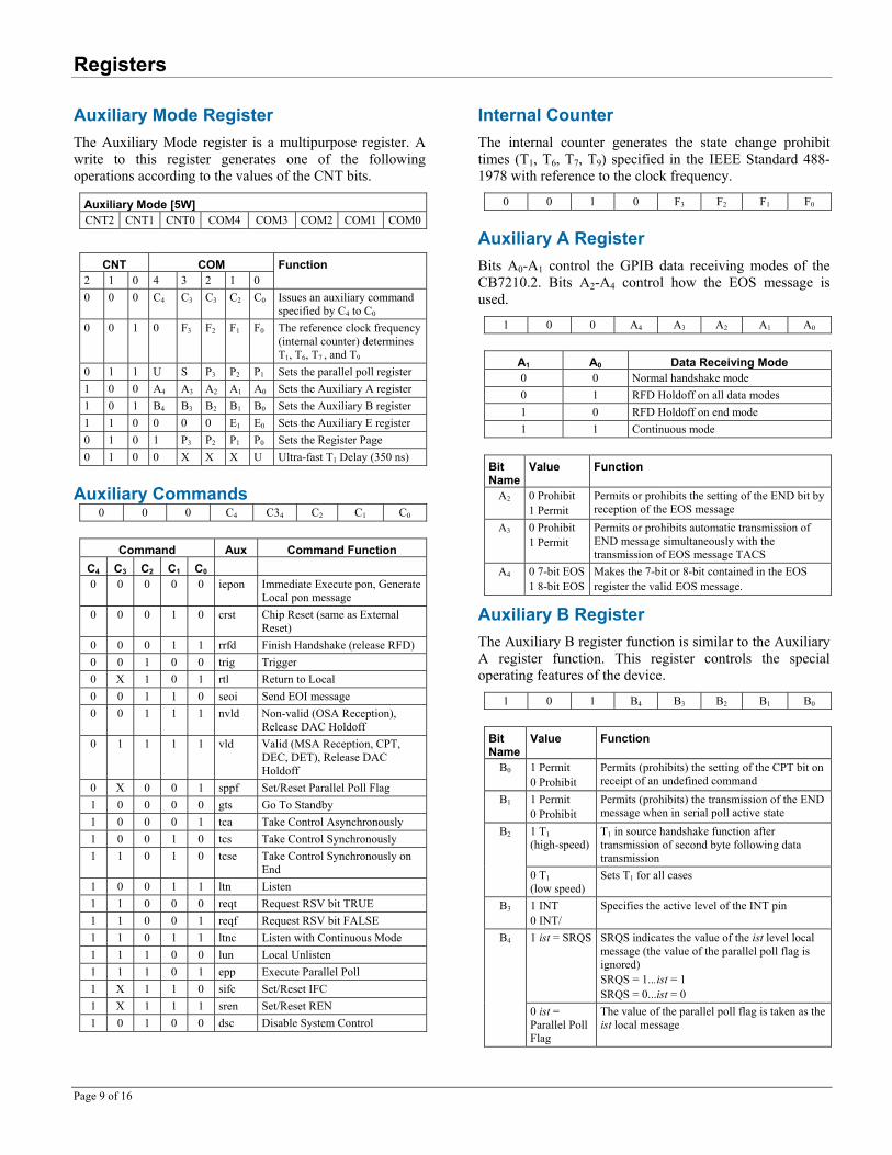
Auxiliary Mode Register Internal Counter The Auxiliary Mode register is a multipurpose register. A write to this register generates one of the following operations according to the values of the CNT bits.
The internal counter generates the state change prohibit times (T1, T6, T7, T9) specified in the IEEE Standard 488-1978 with reference to the clock frequency.
Auxiliary Mode [5W] CNT2 CNT1 CNT0 COM4 COM3 COM2 COM1 COM0
0 0 1 0 F3 F2 F1 F0
Auxiliary A Register CNT COM
2 1 0 4 3 2 1 0 Function
0 0 0 C4 C3 C3 C2 C0 Issues an auxiliary command specified by C4 to C0
0 0 1 0 F3 F2 F1 F0 The reference clock frequency (internal counter) determines T1, T6, T7 , and T9
0 1 1 U S P3 P2 P1 Sets the parallel poll register 1 0 0 A4 A3 A2 A1 A0 Sets the Auxiliary A register 1 0 1 B4 B3 B2 B1 B0 Sets the Auxiliary B register 1 1 0 0 0 0 E1 E0 Sets the Auxiliary E register 0 1 0 1 P3 P2 P1 P0 Sets the Register Page 0 1 0 0 X X X U Ultra-fast T1 Delay (350 ns)
Bits A0-A1 control the GPIB data receiving modes of the CB7210.2. Bits A2-A4 control how the EOS message is used.
1 0 0 A4 A3 A2 A1 A0
A1 A0 Data Receiving Mode 0 0 Normal handshake mode 0 1 RFD Holdoff on all data modes 1 0 RFD Holdoff on end mode 1 1 Continuous mode
Bit Name
Value Function
A2 0 Prohibit 1 Permit
Permits or prohibits the setting of the END bit by reception of the EOS message
A3 0 Prohibit 1 Permit
Permits or prohibits automatic transmission of END message simultaneously with the transmission of EOS message TACS
A4 0 7-bit EOS1 8-bit EOS
Makes the 7-bit or 8-bit contained in the EOS register the valid EOS message.
Auxiliary Commands 0 0 0 C4 C34 C2 C1 C0
Command Aux Command Function
C4 C3 C2 C1 C0 0 0 0 0 0 iepon Immediate Execute pon, Generate
Local pon message 0 0 0 1 0 crst Chip Reset (same as External
Reset) 0 0 0 1 1 rrfd Finish Handshake (release RFD) 0 0 1 0 0 trig Trigger 0 X 1 0 1 rtl Return to Local 0 0 1 1 0 seoi Send EOI message 0 0 1 1 1 nvld Non-valid (OSA Reception),
Release DAC Holdoff 0 1 1 1 1 vld Valid (MSA Reception, CPT,
DEC, DET), Release DAC Holdoff
0 X 0 0 1 sppf Set/Reset Parallel Poll Flag 1 0 0 0 0 gts Go To Standby 1 0 0 0 1 tca Take Control Asynchronously 1 0 0 1 0 tcs Take Control Synchronously 1 1 0 1 0 tcse Take Control Synchronously on
End 1 0 0 1 1 ltn Listen 1 1 0 0 0 reqt Request RSV bit TRUE 1 1 0 0 1 reqf Request RSV bit FALSE 1 1 0 1 1 ltnc Listen with Continuous Mode 1 1 1 0 0 lun Local Unlisten 1 1 1 0 1 epp Execute Parallel Poll 1 X 1 1 0 sifc Set/Reset IFC 1 X 1 1 1 sren Set/Reset REN 1 0 1 0 0 dsc Disable System Control
Auxiliary B Register The Auxiliary B register function is similar to the Auxiliary A register function. This register controls the special operating features of the device.
1 0 1 B4 B3 B2 B1 B0
Bit Name
Value Function
B0 1 Permit 0 Prohibit
Permits (prohibits) the setting of the CPT bit on receipt of an undefined command
B1 1 Permit 0 Prohibit
Permits (prohibits) the transmission of the END message when in serial poll active state
1 T1 (high-speed)
T1 in source handshake function after transmission of second byte following data transmission
B2
0 T1 (low speed)
Sets T1 for all cases
B3 1 INT 0 INT/
Specifies the active level of the INT pin
1 ist = SRQS SRQS indicates the value of the ist level local message (the value of the parallel poll flag is ignored) SRQS = 1...ist = 1 SRQS = 0...ist = 0
B4
0 ist = Parallel Poll Flag
The value of the parallel poll flag is taken as the ist local message
Page 9 of 16

Registers
Auxiliary E Register The Auxiliary E register function controls the Data Acceptance modes of the CB7210.2.
1 1 0 0 0 0 E1 E0
Bit Name Value Function E0 1 Enable
0 Disable DAC Holdoff by Initiation of DCAS
E1 1 Enable 0 Disable
DAC Holdoff by Initiation of DTAS
Parallel Poll Register The Parallel Poll register function defines the parallel poll response of the CB7210.2.
0 1 1 U S P3 P2 P1
U 1 = No parallel poll response 0 = Parallel poll response
S Specify the status bit polarity 1 = In Phase 0 = Reverse Phase
P3
P2
P1
Specify status bit output line (DIO1-DIO8)
Bus State Register* The Bus State register indicates the current state of all bus control lines. To access the Bus State register, write a Set Page Register command to the Auxiliary Command register.
Bus State [7R] NDAC NRFD DAV REN IFC SRQ EOI ATN
Page 10 of 16

AC Characteristics
In the following table, 1 clock cycle = 50 ns.
TA = 0C to 70C; VCC = 5V ± 10% Limits
Min clock limit (clock + ns = min clock)
Max clock limit (clock + ns = max clock)
Parameter Symbol
clock cycle
ns Min clock clock cycle
ns Max clock
Test Conditions
EOI ↓ → DIO tEODI - 30 30 ns PPSS → PPAS, ATN = True EOI ↓ → T/R1 ↑ tEOT11
- 20 20 ns PPSS → PPAS, ATN = True EOI ↑ → T/R1 ↓ tEOT12
- 25 25 ns PPAS → PPSS, ATN = False ATN ↓ → NDAC ↓ tATND
1 20 70 ns AIDS → ANRS, LIDS ATN ↓ → T/R1 ↓ t ATT1
- 30 30 ns TACS + SPAS → TADS, CIDS ATN ↓ → T/R2 ↓ tATT2
- 30 30 ns TACS + SPAS → TADS, CIDS DAV ↓ → DRQ tDVRQ
1 30 80 ns ACRS → ACDS, LACS DAV ↓ → NRFD ↓ tDVNR1 - 10 10 ns ACRS → ACDS DAV ↓ → NDAC ↑ tDVND1 - 45 45 ns ACRS → ACDS → AWNS DAV ↑ → NDAC ↓ tDVND2 1 ½ 20 95 ns AWNS → ANRS DAV ↑ → NRFD ↑ tDVNR2 - 10 10 ns AWNS → ANRS → ACRS RD ↓ → NRFD ↑ tRNR 1 ½ 10 85 ns ANRS → ACRS LACS, DI register selected NDAC ↑ → DRQ ↑ tNDRQ 2 ½ 20 145 ns STRS → SWNS → SGNS, TACS NDAC ↑ → DAV ↑ tNDDV 1 25 75 ns STRS → SWNS → SGNS Address Setup to RD tAR - 20 20 ns RS0 to RS2
CS Address Hold from RD tRA - 0 0 ns RD Pulse Width tRR - 0 0 ns Data Delay from RD ↓ tRD - 15 15 ns Output Float Delay from RD ↑ tDF - 20 20 ns RD Recovery Time tRV 1 0 50 ns Address Setup to WR tAW - 0 0 ns Address Hold from WR tWA - 0 0 ns WR Pulse Width tWW 1 0 50 ns Data Setup to WR tDW - 20 20 ns Data Hold from WR tWD - 0 0 ns WR Recovery Time tRV 1 0 50 ns DRQ ↓ Delay from DACK tAKRQ - 10 10 ns Data Delay from DACK tAKD - 15 15 ns DACK hold time from WR ↑ tDH - 0 0 ns
Page 11 of 16

Timing Waveforms and CPU Interface
DMA Read Timing
tAR tRAtRR
tRD
tRV
tAD
tAKD
tAKRQ
ValidHigh Impedance High Impedance
RD
D -D7 0
DACK
DRQ
CS, RS -RS2 0
tDF
DMA Write Timing
tDH
DRQ
DACK
WR
CPU Read/Write
tAW tWA
tWW
tRV
tDW tWD
D -D7 0
WR
CS,RS -RS2 0
ValidHigh Impedance High Impedance
Page 12 of 16

Timing Waveforms and CPU Interface
CPU Interface You can easily interface the CB7210.2 to common microprocessor or microcomputer chips. A block diagram of the CB7210.2 to an 8085 interface is shown below.
Bus Tranceivers
INT
DRQ DACK
T/R -T/R3 1
CSCLK
RESET
WRRDD-D
70
RS-RS
20
Decoder
H
RESET IN
X1 X2
A -A16 8
AD -AD7 0
IO/M
RD
RESET OUT
CLK
8085
WR
Contact us by phone or email if you need assistance in developing the interface to your particular system. Our engineering staff will work with you to ensure that your CB7210.2 interface is simple, efficient and allows access to all chip features.
Phone: 508-946-5100 and follow the instructions for reaching Tech Support. Email: [email protected]
Page 13 of 16

Transceiver Examples
MC3448A-based transceiver
Data A
Data B
Data C
Data D
S/RA-S/R
D
S/RA
Data A
S/RB
Data B
S/RC
Data C
S/RD
Data D
Bus A
Bus B
Bus C
Bus D
PEA-PE
D
S/RA
Data A
S/RB
Data B
S/RC
Data C
S/RD
Data D
PEA-PE
D
Bus D
Bus C
Bus B
Bus A
Bus A
Bus AData A
Data B
Data C
Data D
Bus B
Bus B
Bus C
Bus C
Bus D
Bus D
PEA-PE
D
DIO8
DIO7
DIO6
DIO5
DIO4
DIO3
DIO2
DIO1
DAV
NRFD
NDAC
SRQ
ATN
REN
IFC
EOI
HL L
CB7210.2 GPIB
S/R -S/RA D PE -PEA D
DIO8
DIO7
DIO6
DIO5
DIO1
DIO4
DIO3
DIO2
T/R1
T/R (EOIOE)3
EOI
DAV
NRFD
NDAC
T/R (CIC)2
SRQ
ATN
REN
IFC
MC3448A
In this example, a high-speed transfer cannot be made, since the bus transceiver is an open collector type.
Page 14 of 16
Transceiver Examples
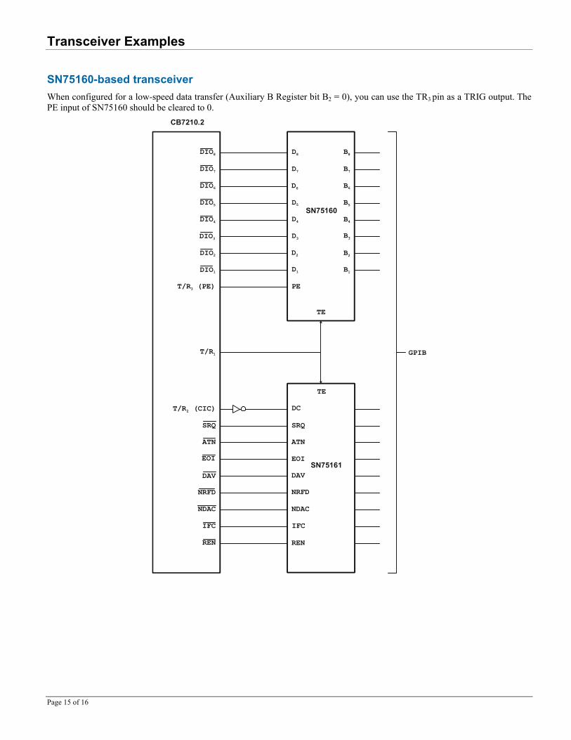
SN75160-based transceiver When configured for a low-speed data transfer (Auxiliary B Register bit B2 = 0), you can use the TR3 pin as a TRIG output. The PE input of SN75160 should be cleared to 0.
D8
D7
D6
D5
D4
D3
D2
D1
PE
DIO8
DIO7
DIO6
DIO5
DIO4
DIO3
DIO2
DIO1
B8
B7
B6
B5
B4
B3
B2
B1
TE
DC
SRQ
ATN
EOI
DAV
NRFD
NDAC
IFC
REN
TE
SN75161
REN
IFC
NDAC
NRFD
DAV
EOI
ATN
SRQ
T/R2 (CIC)
T/R1 GPIB
SN75160
T/R (PE)3
CB7210.2
Page 15 of 16

Package Outlines
CB7210.2-PDIP Item Millimeters
A 51.5 max B 1.62 max C 2.54 ± 0.1 D 0.5 ± 0.1 E 48.26 ± 0.1 F 1.2 min G 2.54 min H 0.5 min I 5.22 max J 5.72 max K 15.24 typ L 13.2 typ M 0.25 (+0.1, -0.05)
A
B C
E
F
H
Side ViewK
L
M 0-15o
D
G
I J
CB7210.2-TQFP Item Min. Nom. Max.
A 12.00 ± 0.2 BSC B 10.00 BSC C 12.00 ± 0.2 BSC D 10.00 BSC E 0.80 BSC F 0.30 mm 0.37 mm 0.45 mm G 0.5 mm 0.10 mm 0.15 mm H 0.09 mm - 0.20 mm I 0.9 mm 1.4 mm 1.9 mm J 11° 12 ° 13° K 0.45 mm 0.65 mm 0.75 mm L 0° - 7° M 0.09R - 0.20R
0.09Rmin
J
KL
M
0 mino
0.20min
H
I
G
1.00
1 11
12
22
2333
34
44
A
B
E F
C D
Page 16 of 16


Measurement Computing Corporation 16 Commerce Boulevard,
Middleboro, Massachusetts 02346 (508) 946-5100
Fax: (508) 946-9500 E-mail: [email protected]
www.mccdaq.com