carrier loss mechanisms in textured crystalline si-based
TRANSCRIPT
1
arXiv preprint
Submitted on July 21, 2017
Carrier loss mechanisms in textured crystalline Si-based solar cells
Akihiro Nakane, Shohei Fujimoto, and Hiroyuki Fujiwaraa)
Department of Electrical, Electronic and Computer Engineering, Gifu University, 1-1
Yanagido, Gifu 501-1193, Japan
Abstract
A quite general device analysis method that allows the direct evaluation of optical and
recombination losses in crystalline silicon (c-Si)-based solar cells has been developed.
By applying this technique, the optical and physical limiting factors of the
state-of-the-art solar cells with ~20% efficiencies have been revealed. In the established
method, the carrier loss mechanisms are characterized from the external quantum
efficiency (EQE) analysis with very low computational cost. In particular, the EQE
analyses of textured c-Si solar cells are implemented by employing the experimental
reflectance spectra obtained directly from the actual devices while using flat optical
models without any fitting parameters. We find that the developed method provides
almost perfect fitting to EQE spectra reported for various textured c-Si solar cells,
including c-Si heterojunction solar cells, a dopant-free c-Si solar cell with a MoOx layer,
and an n-type passivated emitter with rear locally diffused (PERL) solar cell. The
modeling of the recombination loss further allows the extraction of the minority carrier
diffusion length and surface recombination velocity from the EQE analysis. Based on
the EQE analysis results, the carrier loss mechanisms in different types of c-Si solar
cells are discussed.
2
I. INTRODUCTION
Pyramid-shaped textures with sizes of 5~10 µm are generally incorporated into
crystalline silicon (c-Si) solar cells to suppress the front light reflection and thus to
enhance the light absorption in the devices.1,2 The large textures formed on the front and
rear surfaces of the c-Si, however, complicate the optical analysis significantly, making
the determination of the carrier loss mechanisms within the devices quite challenging.
The difficulty of performing the explicit optical characterization arises particularly
from the randomness of the pyramid textures, formed generally by alkaline wet etching
of c-Si (100) wafers.1-3 So far, to characterize the light trapping properties of various
c-Si textures, a computer-intensive ray tracing technique has been applied,1,4-11 but these
studies provide limited success, as the full optical analysis of the multilayered c-Si
device has been rather difficult due to the large calculation cost of this approach. Thus,
there is still a strong need for the development of a novel optical simulator that can be
employed for the practical characterization of textured c-Si devices on a routine basis.
Such a technique is critical for the efficient optimization of solar cells. In particular,
in c-Si heterojunction solar cells, hydrogenated amorphous silicon (a-Si:H) and
transparent conductive oxide (TCO) layers exhibit large unfavorable parasitic
absorption, reducing the external quantum efficiency (EQE) in the short and long
wavelength (λ) regions notably.9-13 For the heterojunction solar cells formed on flat c-Si
substrates, detailed EQE characterization has been performed to determine the optical
losses in the component layers;11 however, for c-Si solar cells with random textures, the
complete optical-loss analysis has not been reported yet.
On the other hand, the effect of the carrier recombination appears clearly in the EQE
spectra of c-Si solar cells, and the intensive carrier recombination observed at a c-Si/Al
rear interface reduces the EQE response in the longer λ region remarkably.14
Accordingly, all the optical and recombination losses in the solar cells can be assessed
quantitatively based on the EQE analysis if the proper analysis method is established.
In our previous study,15-17 we have established an EQE analysis technique for
thin-film solar cells with submicron textures. In this method, to determine the light
absorption in solar cells accurately, reflectance spectra obtained experimentally have
been applied assuming flat optical models within the framework of the optical
admittance method.18 This method provides excellent fittings to numerous EQE spectra
reported for Cu(In,Ga)Se2 (Ref. 15), Cu2ZnSn(S,Se)4 (Ref. 17), and hybrid
perovskite16,19 solar cells, enabling the accurate characterization of the carrier loss
mechanisms in these devices.
3
In this study, to reveal the optical and physical limiting factors of various c-Si-based
solar cells, we have developed a global EQE analysis method in which the light
absorption in the c-Si with a random texture is assessed using the experimental
reflectance spectrum while assuming a perfectly flat optical model. By this procedure,
the EQE calculations of the textured structures are simplified drastically. To reproduce
the incoherent light absorption observed in thick c-Si wafers, a calculation scheme has
also been established. As characterization examples, we present the EQE analyses for (i)
c-Si heterojunction solar cells,9,14,20 (ii) a dopant-free c-Si solar cell21 and (iii) an n-type
passivated emitter with rear locally diffused (PERL) solar cell.22 We have further
developed recombination analysis that can be incorporated into the above EQE analysis.
From our approach, all the reflection, parasitic absorption and recombination losses in
c-Si solar cells can be evaluated systematically.
II. EXPERIMENT
In this study, the EQE spectra of high-efficiency c-Si solar cells reported
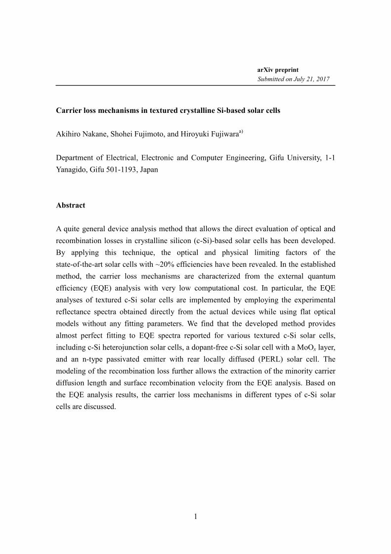
earlier9,14,20-22 have been analyzed. Figure 1 shows the structures of the c-Si solar cells
analyzed by the developed EQE analysis method: flat c-Si heterojunction solar cells
with (a) single-hetero (SH) and (b) double-hetero (DH) structures,14 (c) a textured
a-Si:H/c-Si heterojunction solar cell,20 (d) a textured dopant-free MoOx/c-Si solar cell,21
and (e) a textured n-type PERL solar cell.22 In this figure, the layer thicknesses of the
solar-cell component layers used in the EQE analyses are also indicated. These values
were adopted from the descriptions in the references. In the analyses of Fig. 1(c) and
1(d), however, the a-Si:H layer thicknesses were adjusted slightly to obtain the better
matching with the experimental results, and the original thicknesses are shown inside
the parentheses in Fig. 1. In Table I, the short-circuit current density (Jsc), open-circuit
voltage (Voc), fill factor (FF) and conversion efficiency of the above solar cells,
determined from the current density-voltage characteristics, are summarized.
In the solar cells of Figs. 1(a) and 1(b), hydrogenated amorphous silicon oxide
(a-SiO:H) layers are introduced, instead of conventional a-Si:H layers, to suppress the
detrimental epitaxial growth of an intended a-Si:H layer on c-Si.23 The elimination of
the epitaxial phase at the a-Si:H/c-Si interface is critical to maintain high Voc (Ref. 24)
and the epitaxial phase formation is suppressed quite effectively when a-SiO:H is
employed.23 For the solar cells of Figs. 1(a) and 1(b), the O contents of 7 at.% (p and n
layers) and 4 at.% (i layer) were employed.14 The conversion efficiencies of

4
FIG. 1. Structures of c-Si solar cells analyzed in this study: flat c-Si heterojunction solar
cells with (a) single-hetero (SH) and (b) double-hetero (DH) structures,14 (c) a textured
a-Si:H/c-Si heterojunction solar cell,20 (d) a textured dopant-free MoOx/c-Si solar cell,21
and (e) a textured n-type PERL solar cell.22 The layer thicknesses of the solar-cell
component layers adopted from the references are indicated and these thicknesses were
used in the actual EQE analyses. For (c) and (d), however, the a-Si:H layer thicknesses
were adjusted slightly and the original thicknesses are shown inside the parentheses.
5
TABLE I. Characteristics of c-Si solar cells shown in Fig. 1.
Device Structure Jsc
(mA/cm2)
Voc
(mV)
FF Efficiency
(%)
a-SiO:H/c-Si
(SH) a)
Fig. 1(a) 33.1 643 0.76 16.2
a-SiO:H/c-Si
(DH) a)
Fig. 1(b) 35.6 656 0.75 17.5
a-Si:H/c-Si b) Fig. 1(c) 37.0 718 0.78 20.7
MoOx/c-Si c) Fig. 1(d) 37.1 716 0.73 19.4
PERL d) Fig. 1(e) 41.2 703 0.80 23.2
a) Ref. 14, b) Obtained from Fig. 7 of Ref. 20, c), Ref. 21, d) Ref. 22
a-SiO:H/c-Si solar cells are comparable to those of the a-Si:H/c-Si solar cells.20,23 In
Table I, Jsc of the SH a-SiO:H/c-Si solar cell is lower, compared with the DH structure,
due to the intense carrier recombination at the c-Si/Al rear interface. As known well,1
this rear carrier recombination can be reduced drastically by the introduction of a back
surface field (BSF) structure [i.e., a-SiO:H(i)/a-SiO:H(n) layers in Fig. 1(b)].
The textured a-Si:H/c-Si solar cell in Fig. 1(c) represents a standard structure of c-Si
heterojunction solar cells. Due to the presence of a pyramid-type texture, Jsc of this solar
cell is higher than that of the flat-type solar cell by ~2 mA/cm2. The dopant-free solar
cell architecture [Fig. 1(d)] has been proposed to eliminated the Jsc loss caused by the
parasitic absorption of the a-Si:H p layer in Fig. 1(c), although the a-Si:H i layer is still
necessary to maintain high Voc.21 In this advanced structure, a high work function MoOx
layer is employed as a front contact layer, whereas a LiF tunneling layer is provided as a
rear contact layer. Moreover, to suppress the free carrier absorption in TCO layers,25 the
front TCO of this solar cell has a bilayer structure26 consisting of a high-mobility
In2O3:H (IOH) layer27,28 and a conventional In2O3:Sn (ITO) layer. It should be noted
that the ITO layer in this device is a contact layer, which is employed to reduce contact
resistance with the metal electrode.26
The PERL solar cell [Fig. 1(e)] was fabricated using a surface texture with inverted
pyramids.22 In this device, SiNx antireflection and Al2O3 passivation layers are formed
on the front surface of the p-type emitter (140 Ω/sq). The rear surface of this solar cell is
6
passivated by SiO2 and the rear electrical contact is made through the contact hole
where n+ diffused region is created as the local BSF structure. This solar cell shows a
quite high conversion efficiency of 23.2% with higher Jsc than those of the
heterojunction cells due to the absence of the TCO and a-Si:H-based layers. However,
Voc of the PERL cell is smaller, particularly when compared with a record-efficiency
a-Si:H/c-Si solar cell (Voc=743 mV)29, as the heterointerface suppresses the interface
recombination and the saturation current density effectively.12,13
III. GLOBAL EQE ANALYSIS METHOD
A. Calculation of flat solar cells
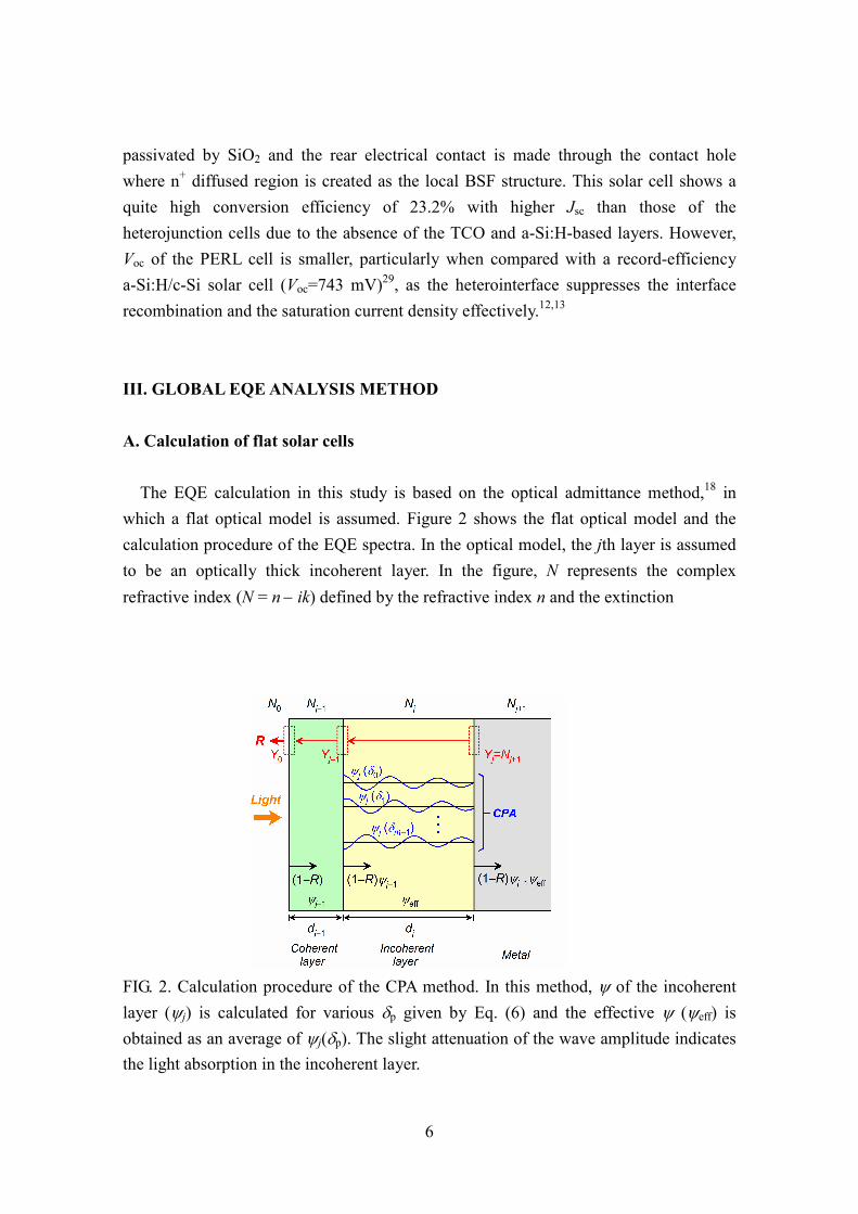
The EQE calculation in this study is based on the optical admittance method,18 in
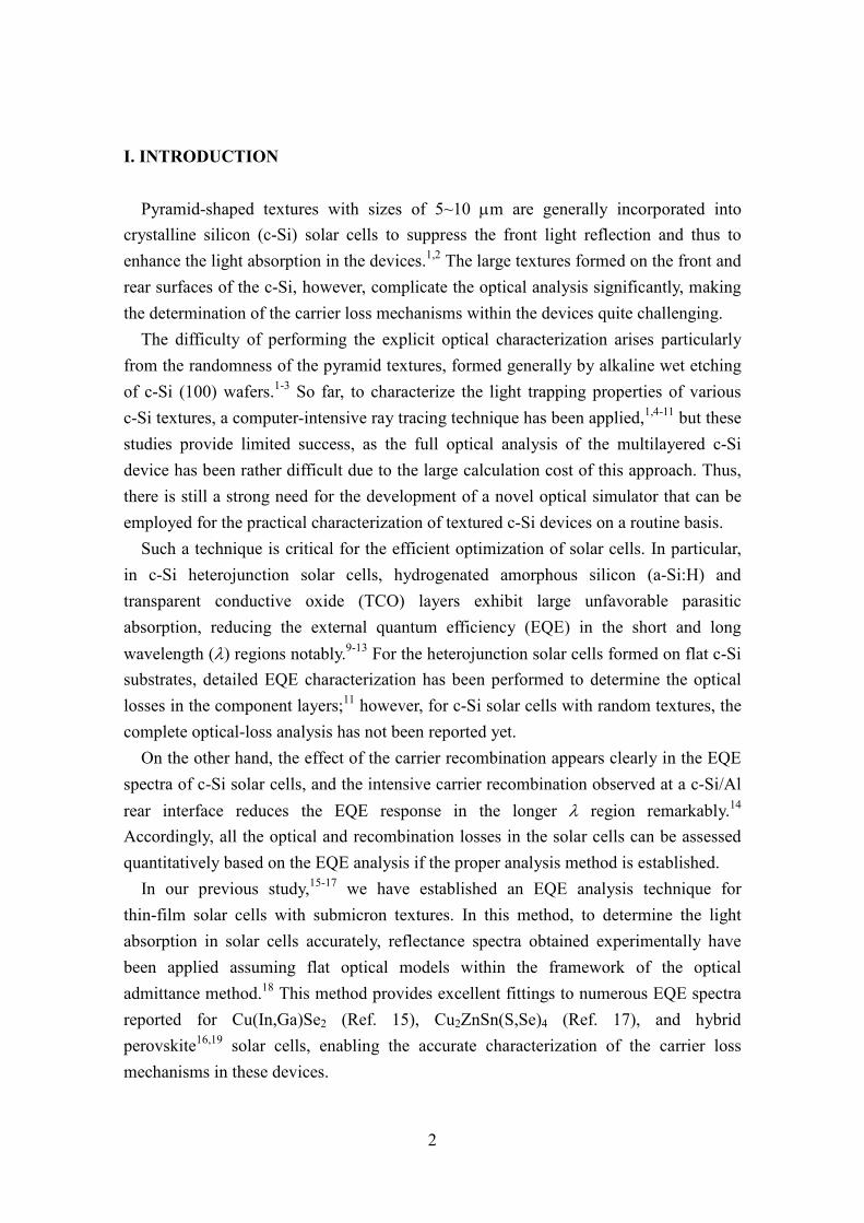
which a flat optical model is assumed. Figure 2 shows the flat optical model and the
calculation procedure of the EQE spectra. In the optical model, the jth layer is assumed
to be an optically thick incoherent layer. In the figure, N represents the complex
refractive index (N = n − ik) defined by the refractive index n and the extinction
FIG. 2. Calculation procedure of the CPA method. In this method, ψ of the incoherent
layer (ψj) is calculated for various δp given by Eq. (6) and the effective ψ (ψeff) is
obtained as an average of ψj(δp). The slight attenuation of the wave amplitude indicates
the light absorption in the incoherent layer.
7
coefficient k.30 The optical admittance Y is expressed as Y = Hf /Ef, where Hf and Ef
show the magnetic and electric fields, respectively. As known well,18,30 there is a
relation of Hf = NEf and thus Y basically corresponds to N. In the case of Fig. 2, we
obtain Yj=Nj+1.
In the conventional optical admittance method applied for optically coherent systems,
Yj is transferred to Yj−1 according to
jjjj
jjjj
jNiY
iNYY
δδ
δδ
sincos
sincos1 +
+=− , (1)
where δj shows the phase thickness expressed by
δj = 2πNjdj/λ. (2)
Here, d and λ are the layer thickness and wavelength, respectively. If the calculation of
Eq. (1) is repeated in a multilayer structure, we obtain Y0 from which the reflectance (R)
of the optical model is calculated as
2
0
2
0 11 YYR +−= . (3)
The important feature of the optical admittance method is that the transmittance (T) at
each interface is obtained by multiplying the potential transmittance ψ of each layer
sequentially from the top layer, and ψj is given by
2
1 sincos)Re(
)Re(
jjjjj
j
j
NiYY
Y
δδψ
+=
−
. (4)
In Fig. 2, T at each interface is indicated and, from R and ψ of each layer, the
absorptance of the jth layer (Aj) is determined as follows:15,17
∏−
=
−−=1
1
)1)(1(j
g
gjj RA ψψ . (5)
For optically thick c-Si wafers (~150 µm), however, the above calculation procedure
cannot be employed because the optical response in this case needs to be calculated
under the incoherent condition. More specifically, for optically thick incoherent layers,
the optical interference is not observed as the phase information is lost completely by
the time-varying phase of light traveling a long distance.30 Quite fortunately, the
calculation procedure for a coherent/incoherent multilayer model has already been
established within the Fresnel approach (or transfer matrix method).31,32 In this method,
the phase δ expressed by Eq. (2) is changed intentionally so that the optical interference
effect is eliminated by averaging out the coherent optical response.
8
By following this approach, we have developed a continuous phase approximation
(CPA) method in which incoherent light absorption is described within the above optical
admittance calculation by varying the phase of the incoherent layer continuously. In the
CPA method, δ of the incoherent layer is expressed by
πλ
πδ
m
pdN jj
p +=2
, (6)
where m is a total number of the assumed waves and p is the sequential number of the
individual wave (p = 0, 1…m−1). In Eq. (6), the term pπ/m indicates a phase added
intentionally to δ of Eq. (2). When the phase is modified, the peak and valley positions
of the propagating waves change [see ψj(δp) in Fig. 2]. Thus, if all the waves having
slightly different δ values are integrated, the optical interference fringes disappear and
the incoherent optical response can be reproduced, as reported previously.31,32
As a result, by modifying Eq. (5), the absorptance of the incoherent layer (Aj,inc) is
described by
( )[ ]∑ ∏−
=
−
=
−−=1
0
1
1, 1)1(
1 m
p
j
g
gpjincj Rm
A ψδψ (7)
∏−
=
−−=1
1eff )1)(1(
j
g
gR ψψ ,
where ψeff indicates the effective ψ of the incoherent layer:
( )∑−
=
=1
0
1 m
p
pjeffm
δψψ . (8)
The above equation confirms that ψeff is a simple average of different ψj(δp) values. The
R of the above incoherent model [i.e., R in Eq. (7)] is further expressed using Eq. (3):
( )( )∑
−
= +
−=
1
0
2
0
0
1
11 m
p p
p
CPAY
Y
mR
δ
δ, (9)
where RCPA shows the reflectance obtained from the CPA method. By applying the
above procedure, the light absorption in a complex multilayer structure with coherent
and incoherent layers can be calculated rather easily. If 100% carrier collection is
further assumed for the incoherent absorber layer, the corresponding EQE spectrum is
obtained from Eq. (7) as Aj,inc(λ)=EQE(λ). In the actual EQE calculation, the c-Si
absorber in the optical model is divided into c-Si sublayers with a thickness of less than
10 µm, as otherwise the computer calculation becomes quite difficult due to quite large
δp values.
9
B. Calculation of textured solar cells
As confirmed previously,33-36 thin film structures formed on the 111 facets of c-Si
pyramid textures can be modeled using a simple coherent optical model. In fact, when a
SiNx or an ITO layer (~70 nm) is deposited on the pyramid-shaped random texture, the
surface shows a blue color, which corresponds to the interference color of the thin film
structure. In other words, light scattering within the thin layers is rather small and the
overall near-surface optical response is described by the coherent condition. In addition,
when the specular light-reflection component of the textures is measured by
spectroscopic ellipsometry (SE) using a tilt-angle optical configuration, a-Si:H/c-Si
solar cell structures deduced by SE show excellent agreement with those determined by
transmission electron microscopy.34,35
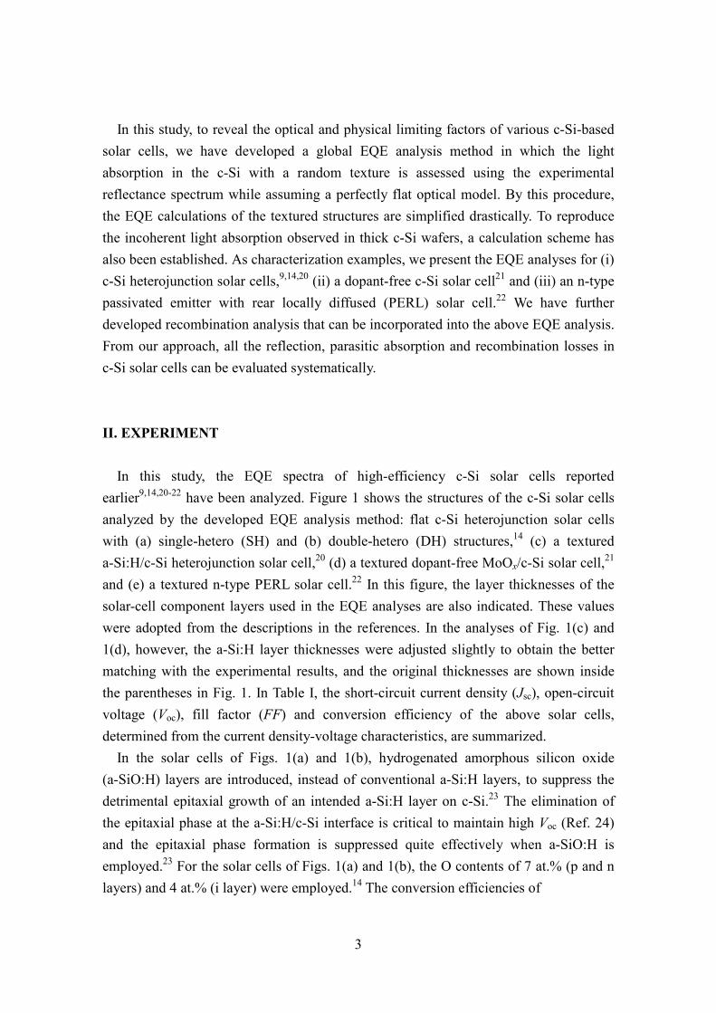
Figure 3(a) schematically shows the light transmission in an ITO/a-Si:H/c-Si front
texture. From experiments, the top angle of the pyramid-shaped texture is confirmed to
be 80o (Refs. 34 and 35). The n values of ITO, a-Si:H and c-Si in the region just above
the band gap (Eg) of c-Si (λ=1100 nm) are n=1.7 (Ref. 25), n=3.6 (Ref. 37), and n=3.5
(Ref. 38), which result in transmission angles of 27o, 12o and 12o, respectively [see Fig.
FIG. 3. (a) Optical transmission in an ITO/a-Si:H thin film structure formed on the
111 facet of a pyramid-shaped c-Si texture and (b) calculation method of the optical
absorption in the textured structure. In this method, a flat optical model is applied while
using the experimental reflectance spectrum (RERS) obtained from an actual textured
solar cell.
10
3(a)]. The transmission angles within the thin layers are close to the normal to the 111
texture-facet plane. Accordingly, based on the above results, we approximate the
absorptance of the TCO and a-Si:H layers incorporated into the textured solar cells by
assuming the normal incidence within the simple coherent condition [see Fig. 3(b)].
Quite fortunately, for this calculation, the identical calculation procedure described in
the previous section (Sec. III A) can be employed. Nevertheless, the c-Si textures reduce
R notably in the visible region, if compared with flat c-Si structures,11 and this
antireflection effect should be taken into account. In this study, to estimate the optical
absorption in c-Si textured solar cells accurately, the reflectance spectra obtained
experimentally from the actual solar cells are adopted for the EQE analyses. These
analyses can be implemented quite easily by replacing R in Eq. (7) with RERS, where
RERS represents R of the experimental reflectance spectra. In other words, if the internal
quantum efficiency (IQE) obtained using a flat optical model is IQEflat, the EQE of the
textured structure (EQEtex) is approximated as
( ) flatERStex 1 IQEREQE −= . (10)
The above procedure simplifies the EQE analysis of textured c-Si solar cells drastically.
In the EQE analysis of the PERL solar cell, on the other hand, the rear interface
structure is assumed to be uniform by neglecting the optical contribution of the local n+
region, as the area fraction of the n+ region is rather small (5%).22
C. Optical constants of solar cell materials
For all the optical analyses in this study, the optical constants of c-Si reported by
Herzinger et al.38 were adopted, whereas the optical data of the Al and Ag rear
electrodes were taken from Ref. 39 and Ref. 40, respectively. In the analyses of the
a-SiO:H/c-Si solar cells [Figs. 1(a) and 1(b)], the optical constants of ITO (Ref. 25) and
a-SiO:H (Ref. 41), extracted from samples fabricated using similar growth conditions,
were used. In particular, the optical carrier concentration (Nopt) of the front and rear ITO
layers in the devices is 5×1020 cm-3 (Refs. 13 and 25).
For the textured a-Si:H/c-Si solar cell in Fig. 1(c), the optical constants of the a-Si:H
and ITO layers incorporated into the solar cells have been characterized by SE9 and
these optical data were adopted for the calculation. In the analysis of Fig. 1(c), however,
we assumed that the optical properties of the a-Si:H i-n layers are identical. Moreover,
based on Ref. 10, the carrier concentrations of the front and rear ITO layers are further
assumed to be 2.4×1020 cm-3 and 1.7×1019 cm-3, respectively.
For the EQE analysis of the dopant-free solar cell [Fig. 1(d)], the reported optical
11
constants of a-Si:H (Ref. 9), ITO (Nopt=2.4×1020 cm-3 of Ref. 10), IOH (Nopt=2.1×10²⁰
cm-3 of Ref. 42) and LiF (Ref. 43) were used, whereas we employed a MoOx dielectric
function extracted from a sputtered MoOx layer40 for the calculation.
In the EQE analysis of the PERL cell [Fig. 1(e)], the dielectric functions of a
wide-gap Si3N4 layer44 and an Al2O3 layer prepared by atomic layer deposition45 were
employed. The parameterization of the Si3N4 dielectric function using the Tauc-Lorentz
model46 leads to A=150.733 eV, E0=8.416 eV, C=3.962 eV, Eg=4.825 eV and
ε1(∞)=1.478. For the actual calculation of the Si3N4 dielectric function, these parameters
were employed. For the SiO2 passivation layer, we used the optical constants of a
thermal oxide formed on c-Si.38
IV. RESULTS
A. Analysis of flat heterojunction solar cells
To confirm the validity of the CPA method, the EQE spectrum of the DH
a-SiO:H/c-Si solar cell without texture [i.e., Fig. 1(b)] was analyzed first. Figure 4
shows the experimental EQE spectrum of this solar cell reported in Ref. 14 (open
circles) and the calculated EQE spectra (solid lines). In this analysis, the EQE of the
c-Si was deduced from Eq. (7) using m=13 assuming 100% carrier collection
(Aj,inc=EQE). The red line represents the EQE spectrum calculated from the CPA method,
whereas the EQE spectra obtained using selected δp values (i.e., p=0, 1, 2, 12) are also
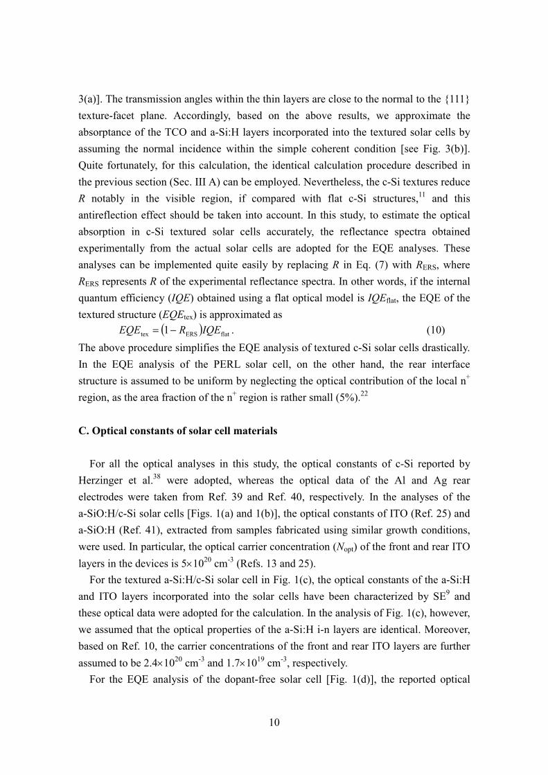
shown (see also the enlarged figure). For the choice of m, we find that (i) a prime
number and (ii) a larger m value are favorable to eliminate the interference fringes
effectively.
As shown in Fig. 4, when the EQE is calculated using a fixed δp, quite sharp optical
interference appears particularly in a low light absorption region of c-Si (λ>1000 nm)
and the interference pattern changes systematically with δp. If the average optical
absorption is calculated from Eq. (7), therefore, all the sharp absorption features are
averaged out and a quite smooth incoherent spectrum can be obtained.
Figure 5 shows the EQE analysis result for the flat DH a-SiO:H/c-Si solar cell. The
experimental EQE (open circles) and the EQE calculated from the CPA method (red
line) are consistent with Fig. 4, whereas the black lines indicate the CPA-derived
reflectance spectrum (RCPA) and absorptance spectra of the solar-cell component layers.
In Fig. 5, the calculated EQE spectrum shows almost perfect agreement with the
experimental EQE spectrum in the wide λ region. As a result, Jsc obtained from the CPA
12
FIG. 4. Experimental EQE spectrum (open circles) and calculated EQE spectra (solid lines) of the flat a-SiO:H/c-Si solar cell (DH) shown in Fig. 1(b). The experimental spectrum was taken from Ref. 14. For the EQE spectra calculated using fixed δp values, only the results of p=0, 1, 2 and 12 (m=13) are shown for clarity. The values inside the parentheses show δ added intentionally [see Eq. (6)]. The red line represents the EQE spectrum calculated by applying the CPA method. The enlarged spectra in the range of 1000≤λ≤1100 nm are also shown.
FIG. 5. EQE analysis result for the flat a-SiO:H/c-Si solar cell (DH) shown in Fig. 1(b). The experimental EQE (open circles) and the calculated EQE (red line) are consistent with Fig. 4. The black lines indicate the reflectance spectrum and absorptance spectra of the solar-cell component layers, deduced from the CPA method.
13
calculation (34.9 mA/cm2) agrees quite well with the experimental Jsc (35.4 mA/cm2).
We emphasize that the above EQE analysis was implemented without using any
fitting parameters. In particular, the a-SiO:H/c-Si solar cell was fabricated by real-time
control of the a-SiO:H layer thicknesses using SE with an accuracy of ~1 Å,47 and the
structural uncertainty is quite small for this solar cell. The excellent agreement observed
between the experimental and calculated EQE spectra confirms that the a-SiO:H layers
are “dead layers” that allow almost no carrier extraction.
The above EQE analysis shows clearly that the parasitic absorption in the front
structure [i.e., ITO/a-SiO:H(p-i)] is relatively large with a total loss of 2.3 mA/cm2,
while the rear structure [i.e., a-SiO:H(i-n)/ITO/Al] shows a very small optical loss of
0.4 mA/cm2. In this solar cell, however, the largest Jsc loss occurs by the reflectance loss
(8.9 mA/cm2) due to the flat device structure.
To justify the CPA approach further, flat a-Si:H/c-Si solar cells reported in Ref. 11
were analyzed. These solar cells have a structure of ITO/a-Si:H p (5 nm)/a-Si:H i (5
nm)/c-Si (280 µm)/a-Si:H n (9 nm)/Ag, and a series of the solar cells were made by
varying the ITO layer thickness (53~93 nm). For the EQE analyses, dielectric functions
of a-Si:H processed at 130 oC (Ref. 37) and ITO (Nopt=4.9×1020 cm-3) of Ref. 25 were
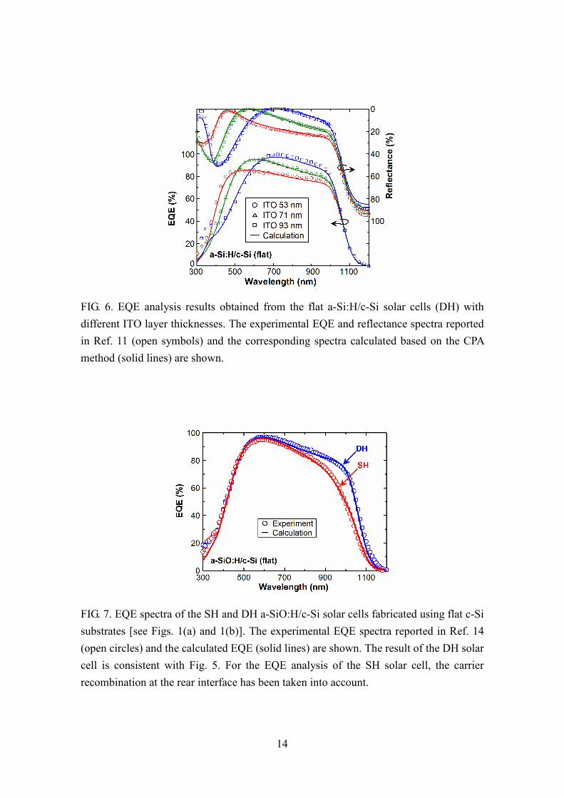
employed. Figure 6 summarizes the experimental EQE and reflectance spectra (open
symbols) and the corresponding spectra calculated based on the CPA method (solid
lines). For all the EQE and reflectance spectra, remarkable agreement has been observed.
Thus, RCPA obtained from Eq. (9) provides good matching to the experimental result.
The above result further supports that only the photocarriers generated within c-Si
contribute to Jsc and those created within the a-Si:H layers are lost by recombination.
Our result is slightly different from those of earlier studies in which slight carrier
extraction (~30%) from a-Si:H i layers is reported to occur.9,11
B. Modeling of carrier recombination
By extending the CPA method, we have further characterized the carrier
recombination observed in the SH a-SiO:H/c-Si solar cell without a BSF structure14 [i.e.,
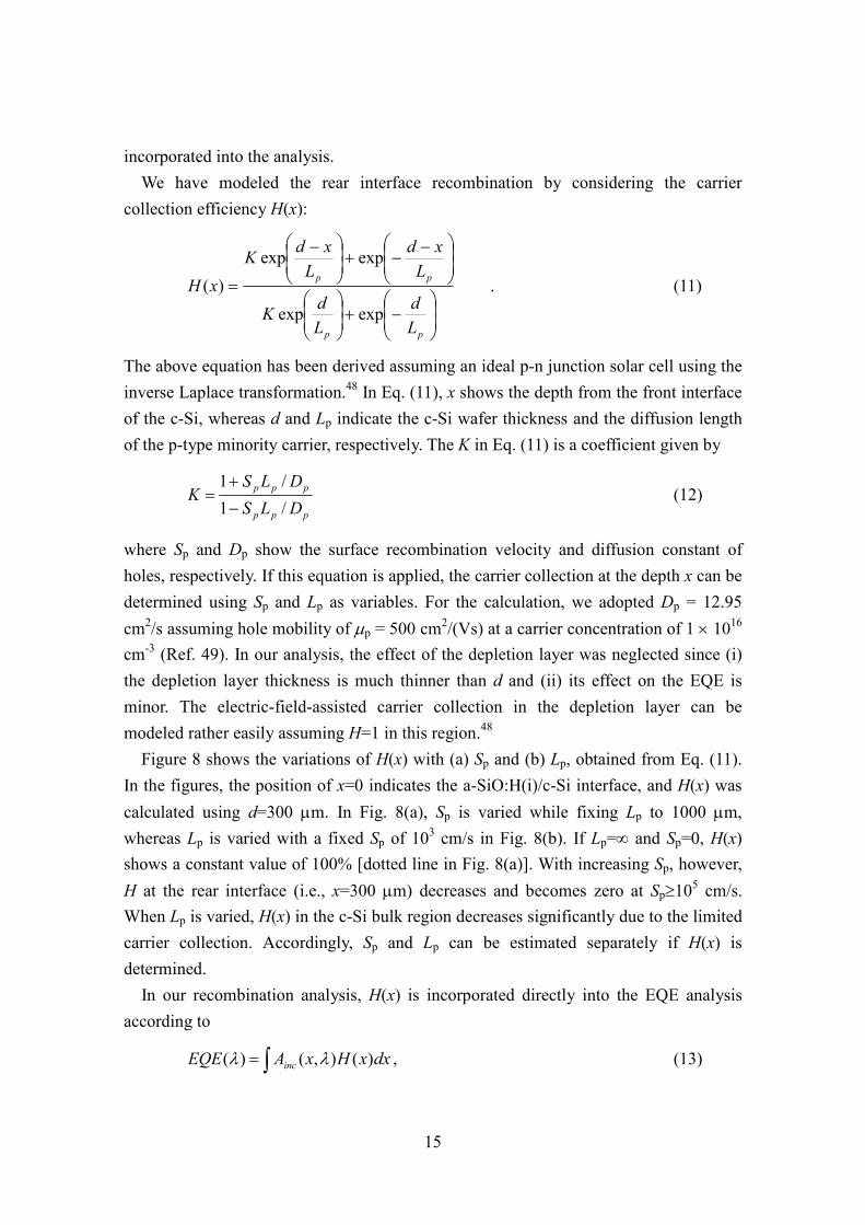
Fig. 1(a)]. Figure 7 compares the EQE spectra obtained from the SH and DH
a-SiO:H/c-Si solar cells of Figs. 1(a) and 1(b). In Fig. 7, the experimental EQE
spectrum (open circles) of the SH solar cell shows the lower EQE response in the long λ
region (λ > 700 nm), compared with the DH solar cell, due to the effect of the rear
interface recombination. In this case, therefore, the recombination effect needs to be
14
FIG. 6. EQE analysis results obtained from the flat a-Si:H/c-Si solar cells (DH) with
different ITO layer thicknesses. The experimental EQE and reflectance spectra reported
in Ref. 11 (open symbols) and the corresponding spectra calculated based on the CPA
method (solid lines) are shown.
FIG. 7. EQE spectra of the SH and DH a-SiO:H/c-Si solar cells fabricated using flat c-Si
substrates [see Figs. 1(a) and 1(b)]. The experimental EQE spectra reported in Ref. 14
(open circles) and the calculated EQE (solid lines) are shown. The result of the DH solar
cell is consistent with Fig. 5. For the EQE analysis of the SH solar cell, the carrier
recombination at the rear interface has been taken into account.
15
incorporated into the analysis.
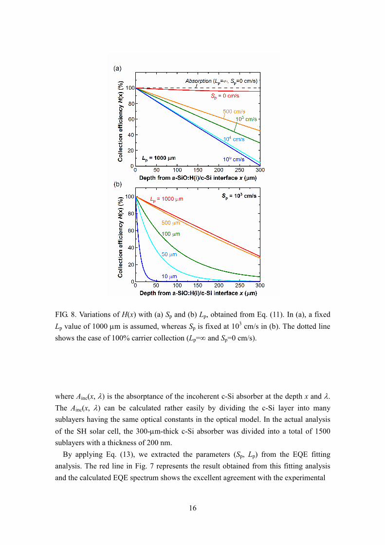
We have modeled the rear interface recombination by considering the carrier
collection efficiency H(x):
−+
−−+
−
=
pp
pp
L
d
L
dK
L
xd
L
xdK
xH
expexp
expexp
)( . (11)
The above equation has been derived assuming an ideal p-n junction solar cell using the
inverse Laplace transformation.48 In Eq. (11), x shows the depth from the front interface
of the c-Si, whereas d and Lp indicate the c-Si wafer thickness and the diffusion length
of the p-type minority carrier, respectively. The K in Eq. (11) is a coefficient given by
ppp
ppp
DLS
DLSK
/1
/1
−
+= (12)
where Sp and Dp show the surface recombination velocity and diffusion constant of
holes, respectively. If this equation is applied, the carrier collection at the depth x can be
determined using Sp and Lp as variables. For the calculation, we adopted Dp = 12.95
cm2/s assuming hole mobility of µp = 500 cm2/(Vs) at a carrier concentration of 1 × 10¹⁶
cm-3 (Ref. 49). In our analysis, the effect of the depletion layer was neglected since (i)
the depletion layer thickness is much thinner than d and (ii) its effect on the EQE is
minor. The electric-field-assisted carrier collection in the depletion layer can be
modeled rather easily assuming H=1 in this region.48
Figure 8 shows the variations of H(x) with (a) Sp and (b) Lp, obtained from Eq. (11).
In the figures, the position of x=0 indicates the a-SiO:H(i)/c-Si interface, and H(x) was
calculated using d=300 µm. In Fig. 8(a), Sp is varied while fixing Lp to 1000 µm,
whereas Lp is varied with a fixed Sp of 103 cm/s in Fig. 8(b). If Lp=∞ and Sp=0, H(x)
shows a constant value of 100% [dotted line in Fig. 8(a)]. With increasing Sp, however,
H at the rear interface (i.e., x=300 µm) decreases and becomes zero at Sp≥105 cm/s.
When Lp is varied, H(x) in the c-Si bulk region decreases significantly due to the limited
carrier collection. Accordingly, Sp and Lp can be estimated separately if H(x) is
determined.
In our recombination analysis, H(x) is incorporated directly into the EQE analysis
according to
∫= dxxHxAEQE inc )(),()( λλ , (13)
16
FIG. 8. Variations of H(x) with (a) Sp and (b) Lp, obtained from Eq. (11). In (a), a fixed
Lp value of 1000 µm is assumed, whereas Sp is fixed at 103 cm/s in (b). The dotted line
shows the case of 100% carrier collection (Lp=∞ and Sp=0 cm/s).
where Ainc(x, λ) is the absorptance of the incoherent c-Si absorber at the depth x and λ.
The Ainc(x, λ) can be calculated rather easily by dividing the c-Si layer into many
sublayers having the same optical constants in the optical model. In the actual analysis
of the SH solar cell, the 300-µm-thick c-Si absorber was divided into a total of 1500
sublayers with a thickness of 200 nm.
By applying Eq. (13), we extracted the parameters (Sp, Lp) from the EQE fitting
analysis. The red line in Fig. 7 represents the result obtained from this fitting analysis
and the calculated EQE spectrum shows the excellent agreement with the experimental
17
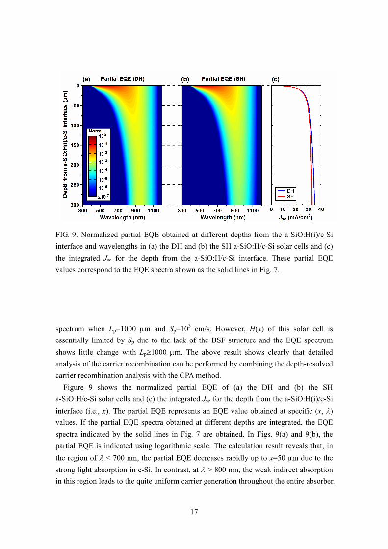
FIG. 9. Normalized partial EQE obtained at different depths from the a-SiO:H(i)/c-Si
interface and wavelengths in (a) the DH and (b) the SH a-SiO:H/c-Si solar cells and (c)
the integrated Jsc for the depth from the a-SiO:H/c-Si interface. These partial EQE
values correspond to the EQE spectra shown as the solid lines in Fig. 7.
spectrum when Lp=1000 µm and Sp=103 cm/s. However, H(x) of this solar cell is
essentially limited by Sp due to the lack of the BSF structure and the EQE spectrum
shows little change with Lp≥1000 µm. The above result shows clearly that detailed
analysis of the carrier recombination can be performed by combining the depth-resolved
carrier recombination analysis with the CPA method.
Figure 9 shows the normalized partial EQE of (a) the DH and (b) the SH
a-SiO:H/c-Si solar cells and (c) the integrated Jsc for the depth from the a-SiO:H(i)/c-Si
interface (i.e., x). The partial EQE represents an EQE value obtained at specific (x, λ)
values. If the partial EQE spectra obtained at different depths are integrated, the EQE
spectra indicated by the solid lines in Fig. 7 are obtained. In Figs. 9(a) and 9(b), the
partial EQE is indicated using logarithmic scale. The calculation result reveals that, in
the region of λ < 700 nm, the partial EQE decreases rapidly up to x=50 µm due to the
strong light absorption in c-Si. In contrast, at λ > 800 nm, the weak indirect absorption
in this region leads to the quite uniform carrier generation throughout the entire absorber.
18
Thus, the influence of the rear-interface carrier recombination appears predominantly in
this λ region. As shown in Fig. 8(a), H decreases almost linearly with x and the partial
EQE of the SH solar cell decreases in the longer λ region, compared with the DH solar
cell. In particular, since Lp (1000 µm) is larger than the absorber thickness (300 µm), the
intense rear-interface recombination reduces the EQE response of the SH solar cell
notably.
In Fig. 9(c), the integrated Jsc values relative to x are shown. The integrated Jsc values
of the SH and DH solar cells are almost identical up to x~50 µm but the recombination
in the SH solar cell hinders the increase in Jsc at x>50 µm, resulting in the Jsc reduction
of 2.5 mA/cm2. The result of Fig. 9 also shows that a stronger optical confinement is
critical to achieve high efficiencies when a thinner c-Si wafer is used.
C. Analysis of textured solar cells
To validate our EQE analysis procedure established for textured c-Si solar cells, a
series of standard a-Si:H/c-Si heterojunction solar cells with different a-Si:H layer
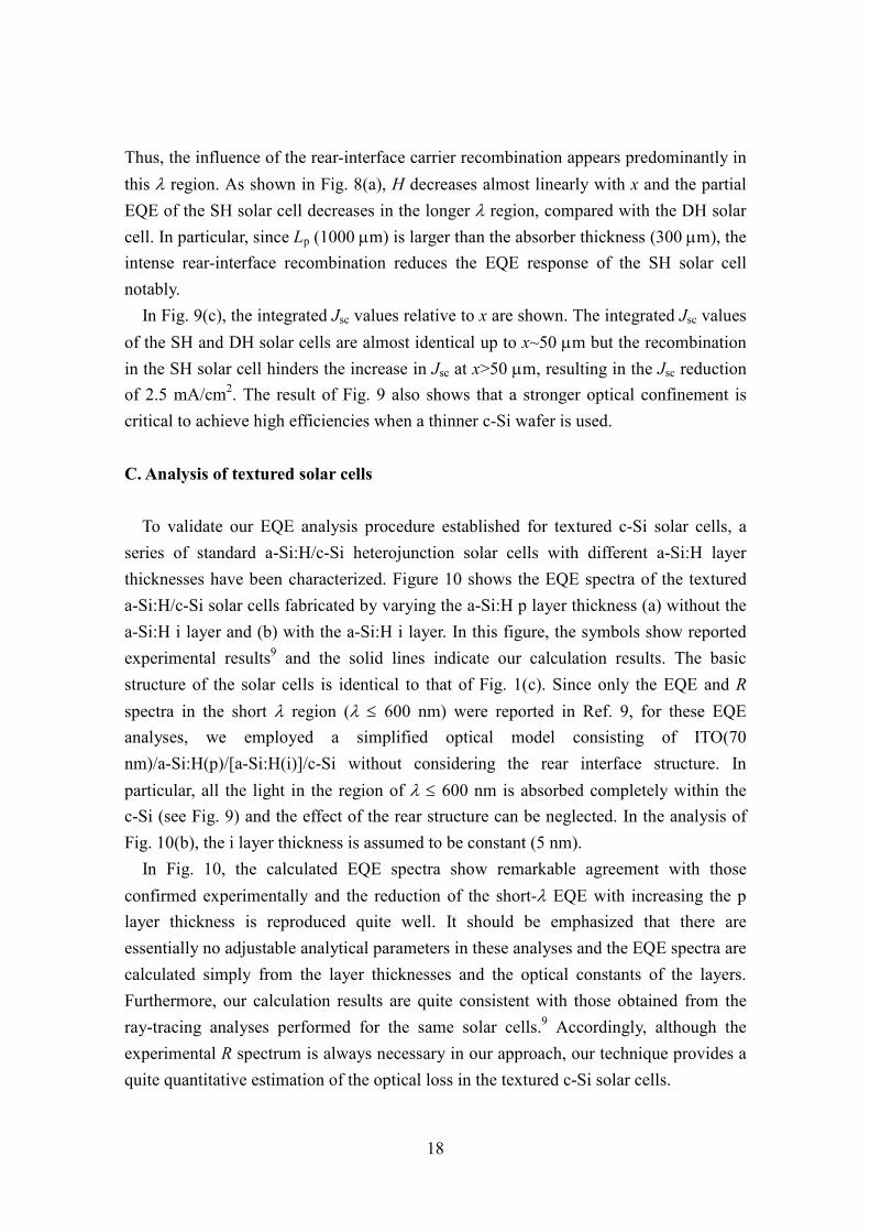
thicknesses have been characterized. Figure 10 shows the EQE spectra of the textured
a-Si:H/c-Si solar cells fabricated by varying the a-Si:H p layer thickness (a) without the
a-Si:H i layer and (b) with the a-Si:H i layer. In this figure, the symbols show reported
experimental results9 and the solid lines indicate our calculation results. The basic
structure of the solar cells is identical to that of Fig. 1(c). Since only the EQE and R
spectra in the short λ region (λ ≤ 600 nm) were reported in Ref. 9, for these EQE
analyses, we employed a simplified optical model consisting of ITO(70
nm)/a-Si:H(p)/[a-Si:H(i)]/c-Si without considering the rear interface structure. In
particular, all the light in the region of λ ≤ 600 nm is absorbed completely within the
c-Si (see Fig. 9) and the effect of the rear structure can be neglected. In the analysis of
Fig. 10(b), the i layer thickness is assumed to be constant (5 nm).
In Fig. 10, the calculated EQE spectra show remarkable agreement with those
confirmed experimentally and the reduction of the short-λ EQE with increasing the p
layer thickness is reproduced quite well. It should be emphasized that there are
essentially no adjustable analytical parameters in these analyses and the EQE spectra are
calculated simply from the layer thicknesses and the optical constants of the layers.
Furthermore, our calculation results are quite consistent with those obtained from the
ray-tracing analyses performed for the same solar cells.9 Accordingly, although the
experimental R spectrum is always necessary in our approach, our technique provides a
quite quantitative estimation of the optical loss in the textured c-Si solar cells.
19
FIG. 10. EQE analysis results obtained for the textured a-Si:H/c-Si solar cells fabricated
by varying the a-Si:H p layer thickness (a) without the a-Si:H i layer and (b) with the
a-Si:H i layer. The experimental EQE spectra reported in Ref. 9 (symbols) and the
calculated EQE (solid lines) are shown.
Conversely, from the EQE analysis of this region, the a-Si:H layer thickness can be
estimated assuming no carrier extraction from the a-Si:H layers.
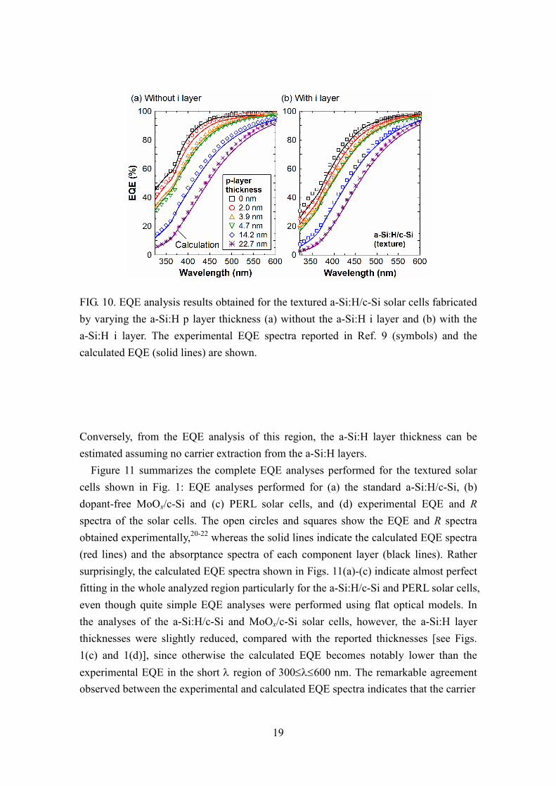
Figure 11 summarizes the complete EQE analyses performed for the textured solar
cells shown in Fig. 1: EQE analyses performed for (a) the standard a-Si:H/c-Si, (b)
dopant-free MoOx/c-Si and (c) PERL solar cells, and (d) experimental EQE and R
spectra of the solar cells. The open circles and squares show the EQE and R spectra
obtained experimentally,20-22 whereas the solid lines indicate the calculated EQE spectra
(red lines) and the absorptance spectra of each component layer (black lines). Rather
surprisingly, the calculated EQE spectra shown in Figs. 11(a)-(c) indicate almost perfect
fitting in the whole analyzed region particularly for the a-Si:H/c-Si and PERL solar cells,
even though quite simple EQE analyses were performed using flat optical models. In
the analyses of the a-Si:H/c-Si and MoOx/c-Si solar cells, however, the a-Si:H layer
thicknesses were slightly reduced, compared with the reported thicknesses [see Figs.
1(c) and 1(d)], since otherwise the calculated EQE becomes notably lower than the
experimental EQE in the short λ region of 300≤λ≤600 nm. The remarkable agreement
observed between the experimental and calculated EQE spectra indicates that the carrier
20
recombination at the rear interface is negligible in these solar cells due to the presence
of the BSF structures.
The result of Fig. 11(d) confirms that the EQE in the short λ region is limited in the
a-Si:H/c-Si and MoOx/c-Si solar cells because of the parasitic light absorption in the
TCO and a-Si:H layers. In the longer λ region, on the other hand, the EQE response of
all the solar cells is quite similar. The R of the PERL cell is, however, quite large,
compared with the heterojunction solar cells, most likely due to the flat rear interface
structure [see Fig. 1(e)].
FIG. 11. EQE analysis results obtained from the textured c-Si solar cells shown in Fig.
1: (a) standard a-Si:H/c-Si, (b) dopant-free MoOx/c-Si and (c) PERL solar cells, and (d)
comparison of the experimental EQE and R spectra. The open circles and squares show
the experimental EQE and R spectra,20-22 respectively. In (a)-(c), the red line indicates
the calculated EQE spectrum, whereas the black lines show the absorptance spectra of
each component layer.
21
V. DISCUSSION
A. Carrier loss mechanisms in textured c-Si solar cells
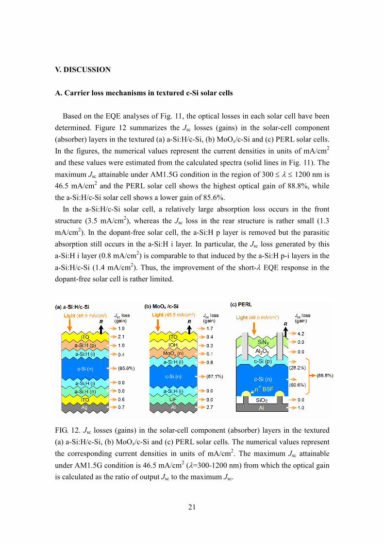
Based on the EQE analyses of Fig. 11, the optical losses in each solar cell have been
determined. Figure 12 summarizes the Jsc losses (gains) in the solar-cell component
(absorber) layers in the textured (a) a-Si:H/c-Si, (b) MoOx/c-Si and (c) PERL solar cells.
In the figures, the numerical values represent the current densities in units of mA/cm2
and these values were estimated from the calculated spectra (solid lines in Fig. 11). The
maximum Jsc attainable under AM1.5G condition in the region of 300 ≤ λ ≤ 1200 nm is
46.5 mA/cm2 and the PERL solar cell shows the highest optical gain of 88.8%, while
the a-Si:H/c-Si solar cell shows a lower gain of 85.6%.
In the a-Si:H/c-Si solar cell, a relatively large absorption loss occurs in the front
structure (3.5 mA/cm2), whereas the Jsc loss in the rear structure is rather small (1.3
mA/cm2). In the dopant-free solar cell, the a-Si:H p layer is removed but the parasitic
absorption still occurs in the a-Si:H i layer. In particular, the Jsc loss generated by this
a-Si:H i layer (0.8 mA/cm2) is comparable to that induced by the a-Si:H p-i layers in the
a-Si:H/c-Si (1.4 mA/cm2). Thus, the improvement of the short-λ EQE response in the
dopant-free solar cell is rather limited.
FIG. 12. Jsc losses (gains) in the solar-cell component (absorber) layers in the textured
(a) a-Si:H/c-Si, (b) MoOx/c-Si and (c) PERL solar cells. The numerical values represent
the corresponding current densities in units of mA/cm2. The maximum Jsc attainable
under AM1.5G condition is 46.5 mA/cm2 (λ=300-1200 nm) from which the optical gain
is calculated as the ratio of output Jsc to the maximum Jsc.
22
Moreover, in the a-Si:H/c-Si solar cell, the optical losses in the rear a-Si:H i-n layers
are zero. This effect can be interpreted by high Eg of a-Si:H layers (~1.7 eV), which lead
to strong light absorption only in the region of λ<730 nm. As confirmed from Fig. 9, all
the light in this region is absorbed in the c-Si upper layer and thus the parasitic
absorption in the rear a-Si:H layers is negligible.
In the MoOx/c-Si solar cell that incorporates the high-mobility IOH layer, the optical
loss induced by the front TCO is well suppressed, compared with the a-Si:H/c-Si solar
cell. In the dopant-free solar cell, however, quite strong parasitic absorption occurs in
the Al rear electrode [see also Fig. 11(b)]. This shows an important fact for the light
absorption in solar cells; i.e., the absorptance of the absorber layer in a multilayer solar
cell is essentially governed by the relative magnitude of the absorption coefficient (α)
and thickness of the component layers. In other words, even when the front optical loss
is reduced, the light absorption in the indirect-transition c-Si absorber may not increase
significantly, if another component layer has a higher α value than that of c-Si. In the
case of the a-Si:H/c-Si solar cell, for example, the contributions of the parasitic
absorption observed at λ > 1000 nm are roughly equal for the front ITO, rear ITO and
Ag, although the light absorption in the front layer tends be larger than the rear layer.
However, if the front parasitic absorption is removed [i.e., Fig. 12(b)], the light
absorption in the rear metal electrode becomes dominant as α of metals is far larger than
that of c-Si. Accordingly, to improve the longer λ response in c-Si solar cells, enhanced
light scattering in the front texture or the increase in the c-Si thickness is necessary.
In the PERL solar cell, the optical loss in the front layers is eliminated completely
and the EQE is equal to 1−R at λ ≤ 1000 nm. Furthermore, there is no carrier loss in the
p-type emitter and its contribution to Jsc (13.1 mA/cm2) accounts for 28% of the total Jsc.
In this solar cell, the largest optical loss occurs by the light reflection (4.2 mA/cm2),
which is notably larger than those in the heterojunction solar cell (~2 mA/cm2) due to
the flat rear interface structure. A ray-tracing simulation of c-Si solar cells has already
confirmed the clear increase in Jsc by double-sided texturing,4 but the rear texturing
makes the formation of the PERL structure more difficult. As mentioned above,
although the optical gain of the PERL cell is high, one disadvantage of this solar cell is
a lower Voc, compared with the heterojunction solar cells.
B. Effect of c-Si thickness
In the above EQE analyses, the c-Si wafer thicknesses of the actual solar cells were
used. However, if the transmission angle depicted in Fig. 3 is assumed, the effective
23
optical pass length within the textured c-Si is expected to increase by 27% [i.e.,
1/cos(50o−12o)], although this effect is neglected completely in our analysis. To find the
effect of c-Si thickness on EQE, we have simulated the EQE spectra of textured
a-Si:H/c-Si solar cells having different wafer thicknesses. For the simulations, we
assumed the a-Si:H/c-Si structure of Fig. 1(c). Unfortunately, the complete device
simulation of c-Si textured structures is difficult in our approach due to the necessity of
the corresponding R spectra, and we employed a fixed R spectrum for all the
calculations. Since R varies with the c-Si thickness, the optical simulation performed
here is hypothetical. However, the change in R observed in a-Si:H/c-Si solar cells in a
thickness range of 100-250 µm is rather small (∆R<5%)10 and the effect of R is
expected to be minor.
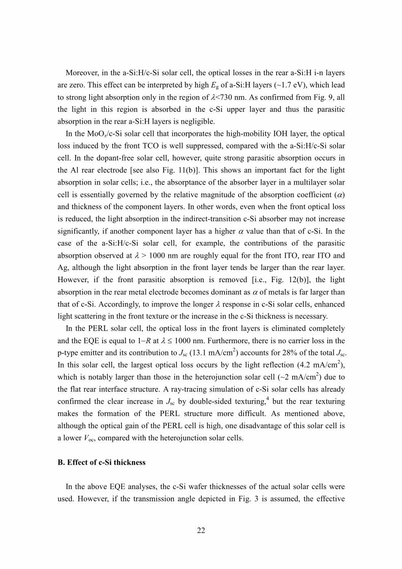
Figure 13 shows the variation of EQE spectrum with c-Si thickness obtained from the
optical simulation. The solid lines show the simulation result, whereas the open symbols
indicate the experimental data of Fig. 11(a).20 With increasing the wafer thickness, the
EQE in the longer λ increases gradually and the experimental EQE shows good
agreement when the c-Si thicknesses in the simulations are 150~200 µm. These
thicknesses are slightly thinner than the actual c-Si thickness (230 µm). If the enhanced
optical pass length by the inclined transition angle (i.e., 27%) is considered for the
230-µm-thick substrate, the effective c-Si thickness becomes ~290 µm. In this case, the
experimental EQE becomes slightly smaller than the simulation result, suggesting the
slight recombination at the rear interface. Nevertheless, the above EQE simulation could
FIG. 13. Variation of EQE spectrum with the c-Si thickness obtained from the optical
simulation. The open circles and squares show the experimental EQE and R spectra
reported in Ref. 20, respectively. In the EQE simulations, R obtained from the
24
a-Si:H/c-Si solar cell with a 230-µm-thick c-Si substrate20 is assumed to be constant.
be too simple to discuss very small carrier losses observed in the longer λ region. Thus,
the effect of the c-Si substrate thickness in textured solar cells needs to be clarified
further based on the EQE analysis results obtained with the variation of the c-Si
thickness.
VI. Conclusion
We established a global EQE analysis method that can be applied for quantitative
analysis of the optical and recombination losses in various c-Si solar cells. In this
calculation scheme, a flat optical model is employed within the framework of the optical
admittance method, and the incoherent optical absorption in thick c-Si substrates is
expressed by using a procedure reported earlier. We find that the EQE calculation of
textured c-Si solar cells can be performed by applying experimental reflectance spectra
to the above method. Our approach provides excellent fittings to numerous EQE spectra
reported for high-efficiency c-Si solar cells fabricated using flat and pyramid-shaped
c-Si substrates. The main advantage of the established method is a very low
computational cost and the EQE calculation can be performed quite easily if the optical
constants and thicknesses of all the layers are known. Based on the EQE analyses, Jsc
losses induced by the front light reflection and parasitic light absorption in solar-cell
component layers were deduced. Furthermore, an EQE analysis procedure that allows
the extraction of the carrier recombination characteristics of the solar cell was
developed. Finally, we note that our method can further be applied to determine carrier
loss mechanisms in multi-junction solar cells consisting of group III-V compound
semiconductors.
25
Reference list
1M. A. Green, Silicon Solar Cells: Advanced Principles & Practice (Centre for
Photovoltaic Devices and Systems, University of New South Wales, 1995). 2W. G. J. H. M. van Sark, L. Korte, F. Roca, editors, Physics and Technology of
Amorphous-Crystalline Heterostructure Silicon Solar Cells (Springer-Verlag, Berlin,
2012). 3E. Vazsonyi, K. De Clercq, R. Einhaus, E. Van Kerschaver, K. Said, J. Poortmans,
J.Szlufcik, and J. Nijs, Sol. Energy Mater. Sol. Cells 57, 179 (1999). 4P. Campbell and M. A. Green, J. Appl. Phys. 62, 243 (1987). 5A. W. Smith and A. Rohatgi, Sol. Energy Mater. Sol. Cells 29, 37 (1993). 6D. Kray, M. Hermle, and S. W. Glunz, Prog. Photovolt. 16, 1 (2008). 7S. C. Baker-Finch and K. R. Mclntosh, Prog. Photovolt. 19, 406 (2011). 8N. Wohrle, J. Greulich, C. Schwab, M. Glatthaar and S. Rein, IEEE J. Photovolt. 3,
175 (2013). 9Z. C. Holman, A. Descoeudres, L. Barraud, F. Z. Fernandez, J. P. Seif, S. De Wolf, and
C. Ballif, IEEE J. Photovolt. 2, 7 (2012). 10Z. C. Holman, M. Filipič, A. Descoeudres, S. De Wolf, F. Smole, M. Topič, and C.
Ballif, J. Appl. Phys. 113, 013107 (2013). 11D. Zhang, I. A. Digdaya, R. Santbergen, R. A. C. M. M. van Swaaij, P. Bronsveld, M.
Zeman, J. A. M. van Roosmalen, and A. W. Weeber, Sol. Energy Mater. Sol. Cells 117,
132 (2013). 12M. Tanaka, M. Taguchi, T. Matsuyama, T. Sawada, S. Tsuda, S. Nakano, H. Hanafusa,
and Y. Kuwano, Jpn. J. Appl. Phys. 31, 3518 (1992). 13H. Fujiwara, and M. Kondo, J. Appl. Phys. 101, 054516 (2007). 14H. Fujiwara, H. Sai, and M. Kondo, Jpn. J. Appl. Phys. 48, 064506 (2009). 15T. Hara, T. Maekawa, S. Minoura, Y. Sago, S. Niki, and H. Fujiwara, Phys. Rev. Appl.
2, 034012 (2014). 16M. Shirayama, H. Kadowaki, T. Miyadera, T. Sugita, M. Tamakoshi, M. Kato, T.
Fujiseki, D. Murata, S. Hara, T. N. Murakami, S. Fujimoto, M. Chikamatsu, and H.
Fujiwara, Phys. Rev. Appl. 5, 014012 (2016). 17A. Nakane, H. Tampo, M. Tamakoshi, S. Fujimoto, K. M. Kim, S. Kim, H. Shibata, S.
Niki, and H. Fujiwara, J. Appl. Phys. 120, 064505 (2016). 18H. A. Macleod, Thin-Film Optical Filters (CRC Press, NY, 2010). 19M. Kato, T. Fujiseki, T. Miyadera, T. Sugita, S. Fujimoto, M. Tamakoshi, M.
Chikamatsu, and H. Fujiwara, J. Appl. Phys. 121, 115501 (2017).
26
20J. P. Seif, A. Descoeudres, M. Filipič, F. Smole, M. Topič, Z. C. Holman, S. De Wolf,
and C. Ballif, J. Appl. Phys. 115, 024502 (2014). 21J. Bullock, M. Hettick, J. Geissbühler, A. J. Ong, T. Allen, C. M. Sutter-Fella, T. Chen,
H. Ota, E. W. Schaler, S. De Wolf, C. Ballif, A. Cuevas, and A. Javey, Nat. Energy 1,
15031 (2015). 22J. Benick, B. Hoex, M. C. M. van de Sanden, W. M. M. Kessels, O. Schultz, and S. W.
Glunz, Appl. Phys. Lett. 92, 253504 (2008). 23H. Fujiwara, T. Kaneko, and M. Kondo, Appl. Phys. Lett. 91, 133508 (2007). 24H. Fujiwara and M. Kondo, Appl. Phys. Lett. 90, 013503 (2007). 25H. Fujiwara and M. Kondo, Phys. Rev. B 71, 075109 (2005). 26L. Barraud, Z. C. Holman, N. Badel, P. Reiss, A. Descoeudres, C. Battaglia, S. De
Wolf, and C. Ballif, Sol. Energy Mater. Sol. Cells 115, 151 (2013). 27T. Koida, H. Fujiwara, and M. Kondo, Sol. Energy Mater. Sol. Cells 93, 851 (2009). 28T. Koida, Phys. Status Solidi A, doi: 10.1002/pssa.201600464 (2016). 29M. A. Green, K. Emery, Y. Hishikawa, W. Warta, E. D. Dunlop, D. H. Levi, and A.
W. Y. Ho-Baillie, Prog. Photovolt. 25, 3 (2017). 30H. Fujiwara, Spectroscopic Ellipsometry: Principles and Applications (Wiley, West
Sussex, UK, 2007). 31M. C. Troparevsky, A. S. Sabau, A. R. Lupini, and Z. Zhang, Opt. Express 18, 24715
(2010). 32R. Santbergen, A. H. M. Smets, and M. Zeman, Opt. Express 21, A262 (2013). 33M. F. Saenger, J. Sun, M. Schädel, J. Hilfiker, M. Schubert, and J. A. Woollam, Thin
Solid Films 518, 1830 (2010). 34K. Watanabe, N. Matsuki, and H. Fujiwara, Appl. Phys. Express 3, 116604 (2010). 35N. Matsuki and H. Fujiwara, J. Appl. Phys. 114, 043101 (2013). 36Y. Tanaka, N. Matsuki, and H. Fujiwara, Thin Solid Films 569, 64 (2014). 37S. Kageyama, M. Akagawa, and H. Fujiwara, Phys. Rev. B 83, 195205 (2011). 38C. M. Herzinger, B. Johs, W.A. McGahan, and J. A. Woollam, J. Appl. Phys. 83, 3323
(1998). 39S. Adachi, The Handbook on Optical Constants of Metals: in Tables and Figures
(World Scientific, Singapore, 2012). 40H. Fujiwara, R. W. Collins, editors, Spectroscopic Ellipsometry for Photovoltaics:
Optical Constants of Solar Cell Materials (Springer, Heidelberg, 2017): in press. 41M. Sato, S. W. King, W. A. Lanford, P. Henry, T. Fujiseki, and H. Fujiwara, J. Non
Cryst. Solids 440, 49 (2016). 42T. Koida, M. Kondo, K. Tsutsumi, A. Sakaguchi, M. Suzuki, and H. Fujiwara, J. Appl.
27
Phys. 107, 033514 (2010). 43E. D. Palik, Handbook of Optical Constants of Solids (Academic Press, New York,
1985). 44H. R. Philipp, J. Electrochem. Soc. 120, 295 (1973). 45G. Dingemans and W. M. M. Kessels, J. Vac. Sci. Technol. A 30, 040802 (2012). 46G. E. Jellison, Jr. and F. A. Modine, Appl. Phys. Lett. 69, 371 (1996); Erratum, Appl.
Phys. Lett. 69, 2137 (1996). 47H. Fujiwara and M. Kondo, Appl. Phys. Lett. 86, 032112 (2005). 48J. Sinkkonen, J. Ruokolainen, P. Uotila, and A. Hovinen, Appl. Phys. Lett. 66, 206
(1995). 49B. L. Anderson and R. L. Anderson, Fundamentals of Semiconductor Devices
(McGraw-Hill, New York, 2005).