carbon nanotubes: - the electrochemical society
TRANSCRIPT

23 The Electrochemical Society Interface • Summer 2006
Carbon Nanotubes:Next Generation of Electronic Materials
The current interest in carbon nanotubes is a direct
consequence of the synthesis of buckminsterfullerene, C60, in 1985 and its derivatives thereafter. The discovery that carbon could form stable, ordered structures other than graphite and diamond stimulated many researchers in the world to search for other allotropes of carbon. This further led to another key finding in 1990 that C60 could be produced in a simple arc-evaporation apparatus readily available in most laboratories. Sumio Iijima1 discovered fullerene-related carbon nanotubes in 1991 using a similar evaporator. The word nanotube is derived from their size, because the diameter of a nanotube is on the order of a few nanometers (approximately 50,000 times smaller than the width of a human hair) and can be up to several micrometers in length. A nanotube (also known as a buckytube) is a member of the fullerene structural family. Nanotubes are composed of sp² bonds, similar to those observed in graphite and they naturally align themselves into ropes held together by van der Waals forces. Carbon nanotubes (CNTs) are cylindrical carbon molecules with novel properties (outstanding mechanical, electrical, thermal, and chemical properties: 100 times stronger than steel, best field emission emitters, can maintain current density of more than 10-9 A/cm², thermal conductivity comparable to that of diamond) which make them potentially useful in a wide variety of applications (e.g., optics, nanoelectronics, composite materials, conductive polymers, sensors, etc.). CNTs are of two types, namely, single-walled carbon nanotubes (SWCNTs) and multiwalled nanotubes (MWCNTs) as shown in Fig.1 (http://www.nanotechnologies.qc.ca/projets/nanotubes). SWCNTs were discovered2 in 1993 and most of these have a diameter close to 1 nm, with a tube length that may be many thousands of times larger and up to orders of centimeters.3 (See the article by Weisman and Subramoney in this issue.)
by Jaldappagari Seetharamappa, Shivaraj Yellappa, and Francis D’Souza
FIG. 1. Structures of (a) SWCNT and (b) MWCNT.
(a) (b)
FIG. 2. 3D model of three types of single-walled carbon nanotubes.
(continued on next page)
The structure of a SWCNT can be conceptualized by wrapping a one-atom-thick layer of graphite (or graphene) into a seamless cylinder. The way the graphene sheet wraps can be represented by a pair of indices (n, m) called the chiral vector. The relationship between n and m defines three categories of CNTs (Fig. 2: http://en.wikipedia.org/wiki/Nanotubes) viz. (i) arm chair (n = m and chiral angle equal to 30°), (ii) zigzag (n = 0 or m = 0 and chiral angle equal to 0°), and (iii) chiral (other values of n and m and chiral angles lie between 0 and 30°). SWCNTs exhibit important electric properties that are not shown by MWCNTs. The most
basic building block of these systems is the electric wire and these are excellent conductors.
SWCNTs were used in the development of the first intramolecular field-effect transistors (FETs) and intramolecular logic gate using SWCNT FETs.4 To create a logic gate, a p-FET and an n-FET are required. Because SWCNTs are p-FETs when exposed to air and n-FETs when unexposed to oxygen, they were able to protect half of a SWCNT from oxygen exposure, while exposing the rest to oxygen. This results in a single SWCNT that acts as a NOT logic gate with both p- and n-type FETs within

24 The Electrochemical Society Interface • Summer 2006
the same molecule. MWCNTs consist of multiple layers of graphite rolled in on themselves to form a tube shape with an interlayer spacing of 3.4 Å. The outer diameter of MWCNTs may range from 1 to 50 nm while the inner diameter is usually of several nanometers. Two models are used to describe the structures of MWCNTs such as the Russian Doll model where the sheets of graphite are arranged in concentric cylinders, e.g., a (0, 8) SWCNT within a larger (0, 10) SWCNT and the Parchment model where a single sheet of graphite is rolled in around itself, resembling a scroll of parchment or a rolled up newspaper.5
The electronic transport in metallic SWCNTs and MWCNTs occurs ballistically (without scattering) over long lengths owing to their nearly one-dimensional electronic structure. This enables nanotubes to carry high currents with negligible heating. It is reported that the MWCNTs can carry high current densities up to 109 to1010 A/cm2 and can conduct current without any measurable change in their resistance or morphology for extended times up to 250°C. The electrical and electronic properties of nanotubes are affected by distortions like bending and twisting. It is extremely challenging to measure the tensile strength of CNTs. Young’s modulus gives
the values of tensile strength and density of CNTs (Table I).
Temperature plays a key role in the strength of CNTs since the motion of dislocations is thermally activated. CNTs are brittle at low temperature, regardless of their diameter and helicity. The specific heat and thermal conductivity of CNTs are dominated by phonons as the electronic contribution is negligible due to low density of free charge carriers. Some parameters of CNTs are shown in Table II.
Preparation and PurificationTechniques like carbon arc-discharge,
laser ablation, high pressure carbon monoxide (HiPco), and chemical vapor deposition (CVD) are being employed to synthesize CNTs of sizeable quantities. Of these, the CVD method has shown the most promise in terms of its price/unit ratio. The arc-evaporation method, which produces the best quality nanotubes, involves applying a current of about 50 A between two graphite electrodes in a helium atmosphere. This results in graphite evaporation, part of which condenses on the walls of the reactor vessel and part on the cathode. Deposit on the cathode usually contains the CNTs. SWCNTs are produced when Co and Ni or some other metal is added to the anode. Ijima and Ichihasti2 have reported the synthesis of SWCNTs with
diameters of around 1 nm by using a gas mixture of 10 Torr methane and 40 Torr argon at a dc current of 200 A and a voltage of 20 V. Bethune et al.7 have used Co, Ni, and Fe as catalysts to synthesize CNTs. Researchers have also used the mixture of catalysts (Ni-Co, Co-Y, or Ni-Y) in the synthesis of SWCNTs. In laser-ablation technique, intense laser pulses are used to ablate a carbon target. The pulsed laser-ablation of graphite in the presence of an inert gas and catalyst yields CNTs8 in the form of ropes or bundles of 5 to 20 nm diameter and tens to hundreds of micrometers long. Fullerenes, graphite polyhedrons with enclosed metal particles, and amorphous carbon were obtained as the by-products in an arc-discharge and a laser-ablation technique. Generally, the CVD technique involves the reaction of a carbon-containing gas (such as methane, acetylene, ethylene, ethanol, etc.) with a metal catalyst particle (usually, cobalt, nickel, iron, or a combination of these such as cobalt/iron or cobalt/molybdenum) at temperatures above 600°C. Although both arc-discharge and laser-ablation methods produce SWCNTs in high yields (more than 70%), they have disadvantages like (i) tangled CNTs that are synthesized to make the purification and applications of CNTs difficult and (ii) these processes rely on evaporation of carbon atoms at temperatures more than 3000°C.
Most SWCNT samples contain carbonaceous impurities such as amorphous carbon, fullerenes, nanoparticles, and transition metals introduced as catalysts during the synthesis of SWCNTs. Proposed applications of SWCNTs, namely, nanoelectronic devices, field emitters, gas sensors, high-strength composites, and hydrogen storage demand pure SWCNT materials. Hence, one of the greatest current demands in carbon nanotube
The Chalkboard(continued from previous page)
Table I. Young’s modulus, tensile strength, and density of carbon nanotubes compared with other materials.
Material Young’s modulus (GPa) Tensile Strength (GPa) Density (g/cm3)
Single wall nanotube 1054.000 150.000
Multiwall nanotube 1200.000 150.000 2.600
Steel 208.000 0.400 7.800
Epoxy 3.500 0.005 1.250
Wood 16.000 0.008 0.600
Table II. Some parameters for carbon nanotubes.6 (All values are for SWCNTs unless otherwise stated.)
Equilibrium Structure
Average diameter of SWNTs 1.2-1.4 nm
Distance from opposite carbon atoms (Line 1) 2.830 Å
Analogous carbon atom separation (Line 2) 2.456 Å
Parallel carbon bond separation (Line 3) 2.450 Å
Carbon bond length (Line 4) 1.420 Å
C-C tight bonding overlap energy ~ 2.50 eV
Group symmetry (10, 10) C5V
Interlayer spacing:(n, n) Armchair(n, 0) Zigzag(2n, n) Chiral
3.380 Å3.410 Å3.390 Å
Optical properties
Fundamental gap:For (n, m); n-m is divisible by 3 [Metallic]For (n, m); n-m is divisible by 3 [Semiconducting]
0 eV~0.5 eV
Maximum current density 1013 A/m2
Thermal transport
Thermal conductivity (room temperature) ~ 2000 W/m K
Phonon mean free path ~ 100 nm
Relaxation time ~ 10-11 s
Elastic behavior
Young's modulus (SWNT) ~ 1 TPa
Young's modulus (MWNT) 1.28 TPa
The Electrochemical Society Interface • Summer 2006 25
research and commercialization includes the development of effective and viable methods for obtaining SWCNTs in pure form without wall damage. The methods adopted include9 hydrothermal, gaseous, or catalytic oxidation, nitric acid reflux, peroxide reflux, cross-flow filtration and chromatography, and chemical functionalization. Although purification based on an initial selective oxidation to remove amorphous carbon followed by a reflux in concentrated nitric acid is effective in removing metal from the reaction products, the refluxing in nitric acid induces wall damage in the nanotubes.9 SWCNTs of more than 90% purity were produced using ultrasonically assisted microfiltration from amorphous and crystalline carbon impurities and metal particle.10 A scalable purification is possible using microwave heating in the presence of air followed by treatment with hydrochloric acid. Microwave assisted purification is also used for purification of MWCNTs.11 Recently, the dissolution of SWCNTs by deoxyribonucleic acid (DNA)12 has been reported.
According to some researchers, the solubilization of SWCNT ropes and bundles in both organic and aqueous solutions is a result of their noncovalent association with polymers. The types of polymers employed in some of the solubilization studies range from the water-soluble helical polymer amylose found in starch, to organic soluble polymers such as poly(m-phenylenevinylene)-co-(2,5-dioctoxy-p-phenylene)vinylene and various derivatives, including poly(2,6-pyridinlenevinylene)-co-(2,5-dioctoxy-p-phenylene)vinylene and poly(5-alkoxy-m-phenylenevinylene)-co-(2,5-dioctoxy-p-phenylene)vinylene.
In addition, carboxymethylcellulose has been employed recently for the purification of SWCNTs. This method involves annealing in air and dispersing the SWCNTs in an aqueous solution of gelatin. The purity of the CNTs can be evaluated by Raman spectroscopy, transmission electron microscopy (TEM), scanning electron microscopy (SEM), atomic force microscopy (AFM), and UV-visble-near-infrared (UV-vis-NIR).
ElectrochemistryThe subtle electronic behavior
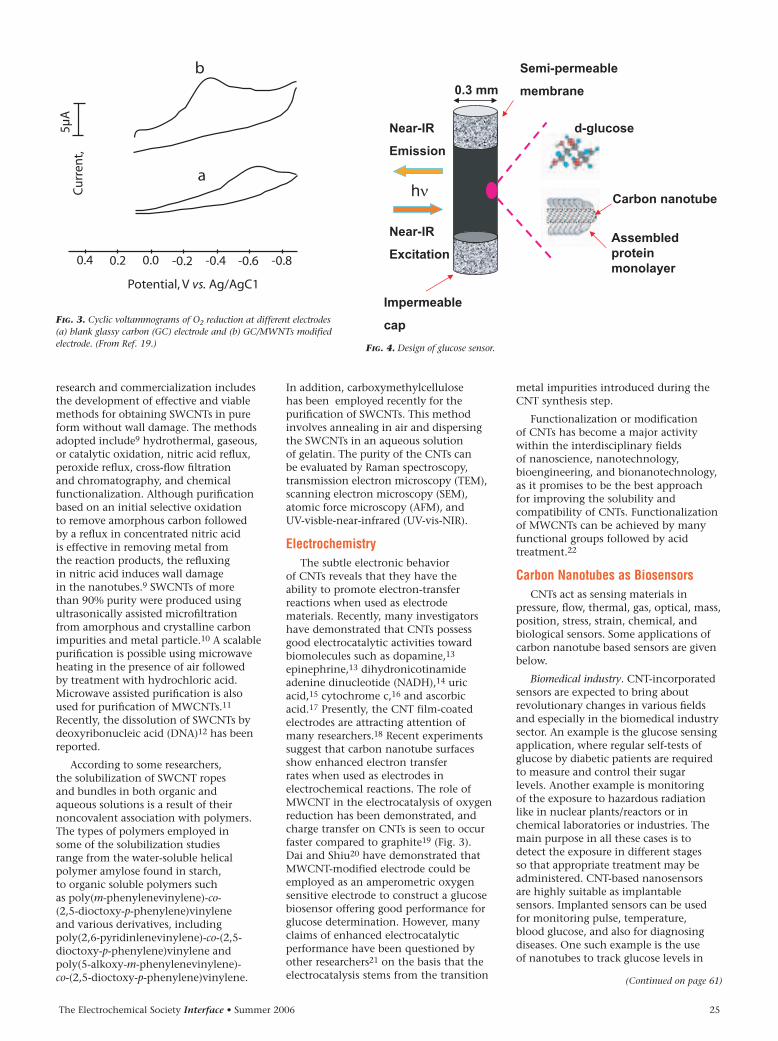
of CNTs reveals that they have the ability to promote electron-transfer reactions when used as electrode materials. Recently, many investigators have demonstrated that CNTs possess good electrocatalytic activities toward biomolecules such as dopamine,13 epinephrine,13 dihydronicotinamide adenine dinucleotide (NADH),14 uric acid,15 cytochrome c,16 and ascorbic acid.17 Presently, the CNT film-coated electrodes are attracting attention of many researchers.18 Recent experiments suggest that carbon nanotube surfaces show enhanced electron transfer rates when used as electrodes in electrochemical reactions. The role of MWCNT in the electrocatalysis of oxygen reduction has been demonstrated, and charge transfer on CNTs is seen to occur faster compared to graphite19 (Fig. 3). Dai and Shiu20 have demonstrated that MWCNT-modified electrode could be employed as an amperometric oxygen sensitive electrode to construct a glucose biosensor offering good performance for glucose determination. However, many claims of enhanced electrocatalytic performance have been questioned by other researchers21 on the basis that the electrocatalysis stems from the transition
metal impurities introduced during the CNT synthesis step.
Functionalization or modification of CNTs has become a major activity within the interdisciplinary fields of nanoscience, nanotechnology, bioengineering, and bionanotechnology, as it promises to be the best approach for improving the solubility and compatibility of CNTs. Functionalization of MWCNTs can be achieved by many functional groups followed by acid treatment.22
Carbon Nanotubes as BiosensorsCNTs act as sensing materials in
pressure, flow, thermal, gas, optical, mass, position, stress, strain, chemical, and biological sensors. Some applications of carbon nanotube based sensors are given below.
Biomedical industry. CNT-incorporated sensors are expected to bring about revolutionary changes in various fields and especially in the biomedical industry sector. An example is the glucose sensing application, where regular self-tests of glucose by diabetic patients are required to measure and control their sugar levels. Another example is monitoring of the exposure to hazardous radiation like in nuclear plants/reactors or in chemical laboratories or industries. The main purpose in all these cases is to detect the exposure in different stages so that appropriate treatment may be administered. CNT-based nanosensors are highly suitable as implantable sensors. Implanted sensors can be used for monitoring pulse, temperature, blood glucose, and also for diagnosing diseases. One such example is the use of nanotubes to track glucose levels in
��� ��� ��� ���� ���� ���� ����
�
��
����
���
���
������������������������
h
RI-raeN
noissimE
RI-raeN
noitaticxE
elbaemrepmI
pac
elbaemrep-imeS
enarbmemmm 3.0
ebutonan nobraC
delbmessAnietorp
reyalonom
esoculg-d
(Continued on page 61)
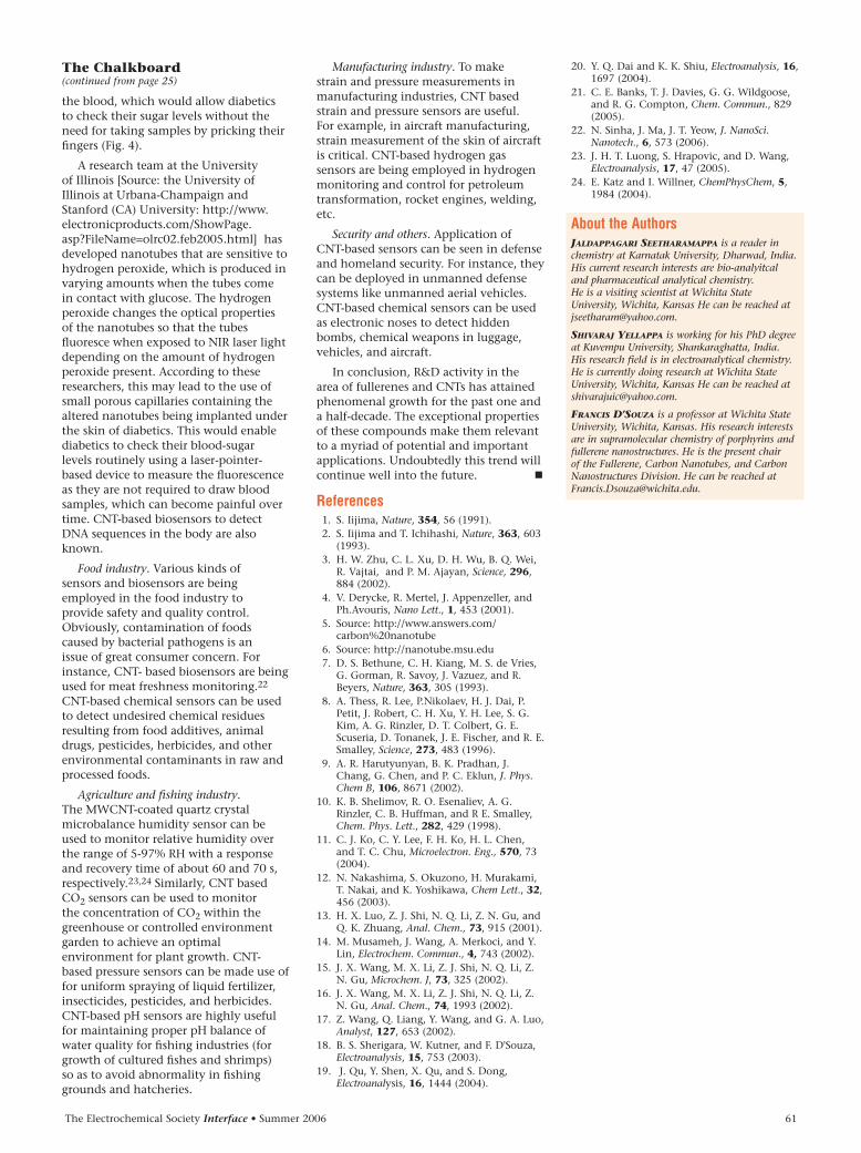
FIG. 3. Cyclic voltammograms of O2 reduction at different electrodes (a) blank glassy carbon (GC) electrode and (b) GC/MWNTs modified electrode. (From Ref. 19.) FIG. 4. Design of glucose sensor.
The Electrochemical Society Interface • Summer 2006 61
the blood, which would allow diabetics to check their sugar levels without the need for taking samples by pricking their fingers (Fig. 4).
A research team at the University of Illinois [Source: the University of Illinois at Urbana-Champaign and Stanford (CA) University: http://www.electronicproducts.com/ShowPage.asp?FileName=olrc02.feb2005.html] has developed nanotubes that are sensitive to hydrogen peroxide, which is produced in varying amounts when the tubes come in contact with glucose. The hydrogen peroxide changes the optical properties of the nanotubes so that the tubes fluoresce when exposed to NIR laser light depending on the amount of hydrogen peroxide present. According to these researchers, this may lead to the use of small porous capillaries containing the altered nanotubes being implanted under the skin of diabetics. This would enable diabetics to check their blood-sugar levels routinely using a laser-pointer-based device to measure the fluorescence as they are not required to draw blood samples, which can become painful over time. CNT-based biosensors to detect DNA sequences in the body are also known.
Food industry. Various kinds of sensors and biosensors are being employed in the food industry to provide safety and quality control. Obviously, contamination of foods caused by bacterial pathogens is an issue of great consumer concern. For instance, CNT- based biosensors are being used for meat freshness monitoring.22 CNT-based chemical sensors can be used to detect undesired chemical residues resulting from food additives, animal drugs, pesticides, herbicides, and other environmental contaminants in raw and processed foods.
Agriculture and fishing industry. The MWCNT-coated quartz crystal microbalance humidity sensor can be used to monitor relative humidity over the range of 5-97% RH with a response and recovery time of about 60 and 70 s, respectively.23,24 Similarly, CNT based CO2 sensors can be used to monitor the concentration of CO2 within the greenhouse or controlled environment garden to achieve an optimal environment for plant growth. CNT-based pressure sensors can be made use of for uniform spraying of liquid fertilizer, insecticides, pesticides, and herbicides. CNT-based pH sensors are highly useful for maintaining proper pH balance of water quality for fishing industries (for growth of cultured fishes and shrimps) so as to avoid abnormality in fishing grounds and hatcheries.
Manufacturing industry. To make strain and pressure measurements in manufacturing industries, CNT based strain and pressure sensors are useful. For example, in aircraft manufacturing, strain measurement of the skin of aircraft is critical. CNT-based hydrogen gas sensors are being employed in hydrogen monitoring and control for petroleum transformation, rocket engines, welding, etc.
Security and others. Application of CNT-based sensors can be seen in defense and homeland security. For instance, they can be deployed in unmanned defense systems like unmanned aerial vehicles. CNT-based chemical sensors can be used as electronic noses to detect hidden bombs, chemical weapons in luggage, vehicles, and aircraft.
In conclusion, R&D activity in the area of fullerenes and CNTs has attained phenomenal growth for the past one and a half-decade. The exceptional properties of these compounds make them relevant to a myriad of potential and important applications. Undoubtedly this trend will continue well into the future.
References 1. S. Iijima, Nature, 354, 56 (1991). 2. S. Iijima and T. Ichihashi, Nature, 363, 603
(1993). 3. H. W. Zhu, C. L. Xu, D. H. Wu, B. Q. Wei,
R. Vajtai, and P. M. Ajayan, Science, 296, 884 (2002).
4. V. Derycke, R. Mertel, J. Appenzeller, and Ph.Avouris, Nano Lett., 1, 453 (2001).
5. Source: http://www.answers.com/carbon%20nanotube
6. Source: http://nanotube.msu.edu 7. D. S. Bethune, C. H. Kiang, M. S. de Vries,
G. Gorman, R. Savoy, J. Vazuez, and R. Beyers, Nature, 363, 305 (1993).
8. A. Thess, R. Lee, P.Nikolaev, H. J. Dai, P. Petit, J. Robert, C. H. Xu, Y. H. Lee, S. G. Kim, A. G. Rinzler, D. T. Colbert, G. E. Scuseria, D. Tonanek, J. E. Fischer, and R. E. Smalley, Science, 273, 483 (1996).
9. A. R. Harutyunyan, B. K. Pradhan, J. Chang, G. Chen, and P. C. Eklun, J. Phys. Chem B, 106, 8671 (2002).
10. K. B. Shelimov, R. O. Esenaliev, A. G. Rinzler, C. B. Huffman, and R E. Smalley, Chem. Phys. Lett., 282, 429 (1998).
11. C. J. Ko, C. Y. Lee, F. H. Ko, H. L. Chen, and T. C. Chu, Microelectron. Eng., 570, 73 (2004).
12. N. Nakashima, S. Okuzono, H. Murakami, T. Nakai, and K. Yoshikawa, Chem Lett., 32, 456 (2003).
13. H. X. Luo, Z. J. Shi, N. Q. Li, Z. N. Gu, and Q. K. Zhuang, Anal. Chem., 73, 915 (2001).
14. M. Musameh, J. Wang, A. Merkoci, and Y. Lin, Electrochem. Commun., 4, 743 (2002).
15. J. X. Wang, M. X. Li, Z. J. Shi, N. Q. Li, Z. N. Gu, Microchem. J, 73, 325 (2002).
16. J. X. Wang, M. X. Li, Z. J. Shi, N. Q. Li, Z. N. Gu, Anal. Chem., 74, 1993 (2002).
17. Z. Wang, Q. Liang, Y. Wang, and G. A. Luo, Analyst, 127, 653 (2002).
18. B. S. Sherigara, W. Kutner, and F. D'Souza, Electroanalysis, 15, 753 (2003).
19. J. Qu, Y. Shen, X. Qu, and S. Dong, Electroanalysis, 16, 1444 (2004).
The Chalkboard(continued from page 25)
20. Y. Q. Dai and K. K. Shiu, Electroanalysis, 16, 1697 (2004).
21. C. E. Banks, T. J. Davies, G. G. Wildgoose, and R. G. Compton, Chem. Commun., 829 (2005).
22. N. Sinha, J. Ma, J. T. Yeow, J. NanoSci. Nanotech., 6, 573 (2006).
23. J. H. T. Luong, S. Hrapovic, and D. Wang, Electroanalysis, 17, 47 (2005).
24. E. Katz and I. Willner, ChemPhysChem, 5, 1984 (2004).
About the AuthorsJALDAPPAGARI SEETHARAMAPPA is a reader in chemistry at Karnatak University, Dharwad, India. His current research interests are bio-analyitcal and pharmaceutical analytical chemistry. He is a visiting scientist at Wichita State University, Wichita, Kansas He can be reached at [email protected].
SHIVARAJ YELLAPPA is working for his PhD degree at Kuvempu University, Shankaraghatta, India. His research field is in electroanalytical chemistry. He is currently doing research at Wichita State University, Wichita, Kansas He can be reached at [email protected].
FRANCIS D’SOUZA is a professor at Wichita State University, Wichita, Kansas. His research interests are in supramolecular chemistry of porphyrins and fullerene nanostructures. He is the present chair of the Fullerene, Carbon Nanotubes, and Carbon Nanostructures Division. He can be reached at [email protected].