carbon nanotubes and its applications
DESCRIPTION
reportTRANSCRIPT
Summer Project Report
Nanoscience and Technology Consortium
A report on
“Overview of Carbon Nanotubes and Applications in Chemical Industry”
Submitted By:-
Ronika Goswami
College: Visvesvaraya National Institute of Technology, Nagpur
Discipline: Chemical Engineering
ACKNOWLEDGEMENT
With due respect, i express my deep sense of gratitude to the Nanoscience
and Technology Consortium for giving us the opportunity to learn deeper
inside the basics of nanotechnology. I am also very thankful to NSTC for
providing us with the very helpful study materials.
I express sincere thanks to Nanoscience and Technology Consortium,
for providing us with a conducive environment and necessary facilities,
allowing us to reach the desired accomplishment.
Ronika Goswami
B.TECH 5TH SEMESTER
CHEMICAL ENGINEERING
VNIT, Nagpur

CONTENTS:
1. Abstract
2. Introduction
What is carbon nanotube? Nano torus Carbon Nanobud
3. Characterisation of nanomaterials
Scanning Electron Microscope Transmission Electron Microscope Atomic Force Microscope Scanning Tunneling Microscpe
4. Properties of CNTs
Electrical Optical Magnetic Field emission Chemical Mechanical Thermal Highly absorbent
5. Types of CNTs
Single-walled Nanotubes Multi-walled nanotubes
6. CNTs strength
7. Synthesis methods of CNTs
Plasma based synthesis methods: Arc discharge method Laser ablation method
Thermal synthesis process: Chemical vapour deposition Plasma enhanced chemical vapour deposition
Ball milling Other methods
8. Purification of CNTs
Gas phase Liquid phase Intercalation

9. Functionalization of CNTs
10. Applications of CNTs
Conductive or reinforced plastics Energy storage Conductive adhesives or connectors CNTs in electronics Molecular electronics Thermal materials Structural composites Fibers and fabrics Catalyst support CNT ceramics Air, water and gas filtration Field emission displays CNT based sensor for various applications MWNT based gas sensor for NH3 SWNT based gas sensor for NO2 CNT sensor array for various gas detection CNT in drug delivery
11. Carbon Nanotubes biofuel
12. Summary
13. References

KEY WORDS:- Carbon nano tubes, Scanning microscopy, multi walled CNTs, arc discharge method, laser ablation method, chemical vapor deposition method.
INTRODUCTION:-
The history of carbon nanotubes is not entirely clear even for those in the science. Therefore, giving proper credit to the person that invented the carbon nanotube has been the subject of several high tech debates among the scientific communities. The initial history of nanotubes started in the 1970s. A preparation of the planned carbon filaments was completed by Morinobu Endo who was earning his Ph.D. at the University of Orleans, France. The growth of these carbon filaments were initially thought to be

the first carbon nanotubes. However, they failed to meet the measurement requirements for width and thus were deemed, eventually, barreleness. In 1991 the true first invention of nanotube was finally made. It seems as though there was a race between Russian nanotechnologists and Sumio Iijima of Japan. The first observation of the multiwalled carbon nanotubes was credited to Iijima. There are some that hold the belief that in the 1950s there was an initial discovery of what could have possibly been seen as the first carbon nanotubes had Roger Bacon had the high powered electron microscope that would have been necessary. He was credited with the first visual impression of the tubes of atoms that roll up and are capped with fullerene molecules, by many scientists in the field. Some state that his discovery just wasn’t taken very seriously at the time because science did not know how this discovery could impact scientific research.
It would be in 1993 that Iijima and Donald Bethune found single walled
nanotubes known as buckytubes. This helped the scientific community
make more sense out of not only the potential for nanotube research, but
the use and existence of fullerenes.

What is carbon nano tube?
Carbon exists in three forms-graphite, diamond and fullerene. Carbon
nano tubes are allotropes of carbon with a cylindrical nano structure. Nano
tubes are members of the fullerene structural family, which also includes
the spherical bucky balls. A fullerene is any molecule composed entirely of
carbon, in the form of a hollow sphere, ellipsoid or tube. Spherical
fullerenes are also called bucky balls. Nano tubes are considered as 1-D
forms of fullerenes because of large length (upto several microns) and
small diameter to the range of few nano meter resulting in large aspect
ratio. Aspect ratio is length to diameter ratio.
The dimensionality of carbon nano tubes is determined by sp3
hybridization. Carbon nano tubes exhibit a spiral conformation called
chirality.
Nanotorus:
A nanotorus is theoretically described as carbon nanotube bent into a torus
(doughnut shape). Nanotori are predicted to have many unique properties,
such as magnetic moments 1000 times larger than previously expected for
certain specific radii. Properties such as magnetic moment, thermal stability
etc. varies widely depending on radius of the torus and radius of the tube.
Carbon-nano-torus
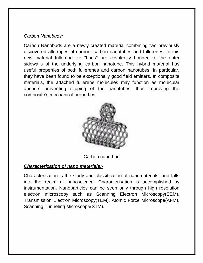
Carbon Nanobuds:
Carbon Nanobuds are a newly created material combining two previously
discovered allotropes of carbon: carbon nanotubes and fullerenes. In this
new material fullerene-like "buds" are covalently bonded to the outer
sidewalls of the underlying carbon nanotube. This hybrid material has
useful properties of both fullerenes and carbon nanotubes. In particular,
they have been found to be exceptionally good field emitters. In composite
materials, the attached fullerene molecules may function as molecular
anchors preventing slipping of the nanotubes, thus improving the
composite’s mechanical properties.
Carbon nano bud
Characterization of nano materials:-
Characterisation is the study and classification of nanomaterials, and falls
into the realm of nanoscience. Characterisation is accomplished by
instrumentation. Nanoparticles can be seen only through high resolution
electron microscopy such as Scanning Electron Microscopy(SEM),
Transmission Electron Microscopy(TEM), Atomic Force Microscope(AFM),
Scanning Tunneling Microscope(STM).

Scanning Electron Microscope(SEM):
Scanning Electron Microscope images the sample surface by scanning it
with a high-energy beam of electrons in a raster scan pattern. Raster scan
pattern is a systematic process of covering the area progressively, one line
at a time by bombarding it with a stream of electrons. This technique is
used in forming images on television screens. The electrons interact with
the atoms that make up the sample producing signals that contain
information about the sample’s surface topography, composition and other
properties such as electrical conductivity. The scanning electron
microscope has many advantages over traditional microscopes. The SEM
has a large depth of field, which allows more of a specimen to be in focus
at one time. The SEM also has much higher resolution, so closely spaced
specimens can be magnified at much higher levels. Because the SEM uses
electromagnets rather than lenses, the researcher has much more control
in the degree of magnification.
Schematic for Scanning Electron microscope

Scanning electron microscope
SEM image of gold nano particle
Transmission Electron Microscope(TEM):
In Transmission Electron Microscope, a beam of electrons is transmitted
through an ultra thin specimen. If the electron gets through, sample is not
very dense in that area. If beam is blocked, sample is densed at that point.
By collecting electron beams onto a screen positioned at the other side of
the sample, an image is formed, giving the exact composition of the
sample. The image is magnified and focused onto an imaging device.
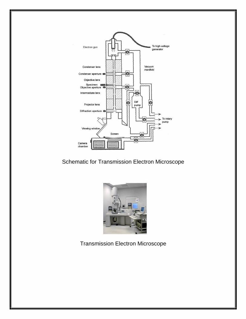
Schematic for Transmission Electron Microscope
Transmission Electron Microscope

TEM image of Brain Cancer Cell
Atomic Force Microscope(AFM):
In Atomic Force Microscope, information is gathered by feeling the surface
with a mechanical probe. A nano-sized tip feels the bumps and troughs on
the surface material. Piezoelectric elements that facilitate tiny but accurate
and precise movements on electronic command enable the very precise
scanning. AFM can also measure the inter-atomic forces using a nano-
Newton scale. In the biomedical field AFM is used to visualize single
biomolecules, live/fixed cells or tissues at nanoscale resolution without
drying/coating them.
Schematic diagram of AFM

Atomic Force Microscope
Scanning Tunneling Microscope(STM):
Scanning Tunneling Microscope generates 3-D images of substances that
conduct electricity. In STM, the structure of a surface is studied using a
stylus that scans the surface at a fixed distance from it. A stylus is a narrow
elongated staff, similar to a modern ball point pen. Stylus generates a very
tiny current, called tunneling current that varies depending upon the
distance of the tip from the surface material. Stylus is mounted on a
piezoelectric tube that is controlled by voltage to expand and contract the
tube to keep tunneling current constant. If the stylus goes into a trough in
surface material, current generated weakens because of extra distance.
Hence, external voltage is applied to the tube to expand it to bring stylus
close to material surface and keep the tunneling current constant. The
movement of the tube is closely monitored and used to generate a 3-D
image of the conducting material.
Schematic for Scanning Tunneling Microscope

PROPERTIES:-
Electrical properties:
CNTs can be highly conducting, and hence can be said to be metallic. Their conductivity has been shown to be a function of their chirality, the degree of twist as well as their diameter. CNTs can be either metallic or semi-conducting in their electrical behavior. Conductivity in MWNTs is quite complex. Some types of ―armchair‖-structured CNTs appear to conduct better than other metallic CNTs. Furthermore, interwall reactions within multi walled nanotubes have been found to redistribute the current over individual tubes non-uniformly. However, there is no change in current across different parts of metallic single-walled nanotubes. The behavior of the ropes of semi-conducting single walled nanotubes is different, in that the transport current changes abruptly at various positions on the CNTs. The conductivity and resistivity of ropes of single walled nanotubes has been measured by placing electrodes at different parts of the CNTs. The resistivity of the single walled nanotubes ropes was of the order of 10–4 ohm-cm at 27°C. This means that single walled nanotube ropes are the most conductive carbon fibers known. The current density that was possible to achieve was 10-7 A/cm2, however in theory the single walled nanotube ropes should be able to sustain much higher stable current densities, as high as 10-13 A/cm2. It has been reported that individual single walled nanotubes may contain defects. Fortuitously, these defects allow the single walled nanotubes to act as transistors. Likewise, joining

CNTs together may form transistor-like devices. A nanotube with a natural junction (where a straight metallic section is joined to a chiral semiconducting section) behaves as a rectifying diode – that is, a half-transistor in a single molecule. It has also recently been reported that single walled nanotubes can route electrical signals at speeds up to 10 GHz when used as interconnects on semi-conducting devices.
Optical properties:
Bulk gold is yellow in colour whereas nano gold is red in colour. The yellow
colour of bulk gold is due to sloshing about of its electron. Metals have a
shine and conduct electricity due to a cloud of free electrons on the surface
of metals, which carry current from one part of the metal to another. The
electron cloud on the surface also absorbs photons without allowing them
to get through. Some photons are reflected, resulting in a shine on the
surface of the metal. Other photons are absorbed by the electron plasma,
resulting in the formation of plasmons. These electron slosh about
particularly well at a particular frequency. All incident photons at or above
this frequency are absorbed and this phenomenon is called surface
Plasmon resonance. Lower frequency light waves are reflected. Smaller
the particle, the higher is its range of absorption of light. As gold particles
are made smaller and smaller, their Plasmon resonance frequency will
become higher, resulting in the range of light that can be absorbed by the
gold particles becoming larger. At macro level, gold absorbs the blue-green
spectrum to be reflected, giving gold its characteristic yellow colour. As
gold size reaches nanoscale, capacity to absorb yellow light also increases,
giving gold nanoparticles a red colour.

Nano gold (red)
Magnetic properties:
At nanoscale, forces in the nucleus become far stronger than at macro
scale. The inter and intra-atomic magnetic forces become exponentially
stronger at nano-level. The magnetism of a material increases per unit area
with a decrease in the size of the material. Magnetic nanoparticles can be
sent into the bloodstream of a person contaminated with bio-toxins, to bind
with the particles of the toxin. Then by utilizing a magnetic field gradient,
the magnetic-toxin particle can be extracted from the body.
Field emission:
Field emission results from the tunneling of electrons from a metal tip into
vacuum, under application of a strong electric field. The small diameter and
high aspect ratio of CNTs is very favorable for field emission. Even for
moderate voltages, a strong electric field develops at the free end of
supported CNTs because of their sharpness. This was observed by de
Heer and co-workers at EPFL in 1995. He also immediately realized that
these field emitters must be superior to conventional electron sources and
might find their way into all kind of applications, most importantly flat-panel
displays. It is remarkable that after only five years Samsung actually
realized a very bright color display, which will be shortly commercialized
using this technology. Studying the field emission properties of multi walled
nanotubes, Bonard and co-workers at EPFL observed that together with
electrons, light is emitted as well. This luminescence is induced by the
electron field emission, since it is not detected without applied potential.
This light emission occurs in the visible part of the spectrum, and can
sometimes be seen with the naked eye.
Chemical properties:
Nanoparticles of titanium oxide is applied for self-cleaning of glass. Glass is
coated with a 15nm thick transparent layer of nanoparticles of titanium
oxide(TiO2). When dust settles on the glass, the reaction of the Ultraviolet
component of sunlight with the coating of nanocrystalline titanium oxide on
the glass causes a reaction that breaks down organic dirt. The coating then
attracts moisture from the atmosphere, forming strongly oxidized free
radicals, which cleans the glass surface.
Mechanical Properties:-
Carbon nanotube is one of the strongest materials in nature. Carbon
nanotubes (CNTs) are basically long hollow cylinders of graphite sheets.
Although a graphite sheet has a 2D symmetry, carbon nanotubes by
geometry have different properties in axial and radial directions. It has been
shown that CNTs are very strong in the axial direction. Young's modulus on
the order of 270 - 950 GPa and tensile strength of 11 - 63 GPa were
obtained.
On the other hand, there was evidence that in the radial direction they are
rather soft. The first transmission electron microscope observation of radial
elasticity suggested that even the van der Waals forces can deform two
adjacent nanotubes. Later, nano indentations with atomic force microscope
were performed by several groups to quantitatively measure radial elasticity
of multi walled carbon nanotubes and tapping/contact mode atomic force
microscopy was recently performed on single-walled carbon nanotubes.
Young's modulus of on the order of several GPa showed that CNTs are in
fact very soft in the radial direction.

Radial direction elasticity of CNTs is important especially for carbon
nanotube composites where the embedded tubes are subjected to large
deformation in the transverse direction under the applied load on the
composite structure.
One of the main problems in characterizing the radial elasticity of CNTs is
the knowledge about the internal radius of the CNT; carbon nanotubes with
identical outer diameter may have different internal diameter (or the
number of walls). Recently a method using atomic force microscope was
introduced to find the exact number of layers and hence the internal
diameter of the CNT. In this way, mechanical characterization is more
accurate.
Thermal properties:
The thermal conductivity of a nanofluid is much greater than that of the
base fluid. Nanoparticles have very high aspect ratio(surface area to
volume ratio). This increase in surface area of the particles is responsible
for higher thermal conductivity in nanofluids.
Highly absorbent:
The large surface area and high absorbency of CNTs make them ideal
candidates for use in air, gas, and water filtration. A lot of research is being
done in replacing activated charcoal with CNTs in certain ultra high purity
applications.
TYPES OF CNTs:-
Carbon nanotubes (CNTs) are allotropes of carbon with
a cylindrical nanostructure. These cylindrical carbon molecules have
unusual properties, which are valuable for
nanotechnology, electronics, optics and other fields of materials
science and technology. In particular, owing to their extraordinary thermal
conductivity and mechanical and electrical properties, carbon nanotubes
find applications as additives to various structural materials.
Nanotubes are members of the fullerene structural family. Their name is derived from their size, since the diameter of a nanotube is of the orders of a few nanometers while they can be upto several millimeters in length. The chemical bonding of nanotubes is composed entirely of sp2 bonds, similar to those of graphite. Nanotubes naturally align themselves into ropes held together by Van der Waal forces. Under high pressure, nanotubes can merge together, trading some sp2 bonds, giving the possibility of producing strong, unlimited-length wires through high pressure nanotube linking.
Nanotubes are categorized as:
Single walled-nanotubes(SWNTs)
Multi-walled nanotubes(MWNTs)
Single walled-nano tubes(SWNTs):
It is conceptualized by wrapping a one-atom-thick layer of graphite called graphene into a seamless cylinder. Most SWNTs have a diameter of close to 1 nm, with a tube length that can be many millions of times longer (limitation possessed by synthesis method). There are ways to roll a grapheme into a single-wall nanotube, some of the resulting nanotubes enabling symmetry mirrors both parallel and perpendicular to the nanotube axis. The way the graphene sheet is wrapped is represented by a pair of indices (n,m) called the chiral vector. The integers n and m denote the number of unit vectors along two directions in the honeycomb crystal lattice of graphene. If m=0, it is known as ―zig-zag‖ nanotube, which is named for the pattern of hexagons as we move on the circumference of the tube. If n=m, it is known as ―armchair‖ nanotube. If value of m lies between zig-zag and armchair, then it is known as chiral. ―Chiral‖ means handedness and it indicates that the tubes may twist in either direction. SWNTs are very expensive. Hence, cheaper means of synthesis are required.

Single walled nanotubes
Multi-walled nanotubes:
Multi-walled nanotubes consist of multiple rolled layers (concentric tubes) of graphite. There are two models which can be used to describe the structures of multi-walled nanotubes. In the Russian Doll model, sheets of graphite are arranged in concentric cylinders, e.g. a (0, 8) single-walled nanotube (SWNT) within a larger (0,10) single-walled nanotube. In the Parchment model, a single sheet of graphite is rolled in around itself, resembling a scroll of parchment or a rolled newspaper. The interlayer distance in multi-walled nanotubes is close to the distance between graphene layers in graphite. Such nanotubes are generally formed either by the electric-arc technique (without any catalyst) or by catalyst-enhanced thermal cracking of gaseous hydrocarbons or CO disproportionation. In Herringbone MWNTs(h-MWNTs), graphenes make an angle with respect to the nanotube axis.
The special place of double-walled carbon nanotubes (DWNT) must be emphasized here because their morphology and properties are similar to SWNT but their resistance to chemicals is significantly improved. This is especially important when functionalization is required (this means grafting of chemical functions at the surface of the nanotubes) to add new properties to the CNT. In the case of SWNT, covalent functionalization will break some C=C double bonds, leaving "holes" in the structure on the nanotube and thus modifying both its mechanical and electrical properties. In the case of DWNT, only the outer wall is modified.

Multi-walled Nanotubes
CNTs’ strength The strength of a material is not as well defined as the Young’s modulus, because it depends not only on the type of material, but also on its history, the atmosphere, the pressure, and the temperature, and the measuring system (fluctuations in load can modify the strength). It is intimately linked to structural defects and imperfections that can be present in the solid and only in very few cases do materials have strengths approaching the theoretical limit. It is usual to distinguish between two kinds of solids associated with two different types of stress/strain curves. The first one is typical of brittle conditions and is characterised by the absence of plasticity, i.e. the rupture occurs in the elastic regime. The strength is measured by the fracture stress σf. Ceramics and glasses usually exhibit a brittle breaking mechanism. The second behaviour is typical of ductile conditions and is encountered in metals and simple ionic solids. The strength of the material is then associated with the yield stress σy when the material ceases to behave elastically. The strength and the breaking mechanisms of a material depend largely on the mobility of dislocations and their ability to relax stress concentrations at the flaw tip. It is frequently observed that the strength of a brittle solid depends on the size of the sample. Graphite whiskers exhibit strength as high as 20 GPa, but the typical strength is 1 GPa for larger fibres . This behaviour is due to the fact that the number of flaws is considerably reduced in whiskers. Griffith showed that in brittle solids, fracture occurs through local decohesion at the tip of an extending sharp crack instead of simultaneous bond breaking across the whole fracture plane. This is why real strengths are orders of magnitude lower than theoretical ones.With CNTs, we have in hand model systems to study

the intrinsic strength of a sp2 bonded material and how it relaxes the mechanical energy at high strain. We recall that the temperature is an important parameter in the strength of a material since the motion of dislocations is thermally activated. Like all covalent materials, CNTs are brittle at low temperature, whatever their diameter and helicity. The flexibility of CNTs at room temperature is not due to any plastic deformation but to their high strength and to the unique capability of the hexagonal network to distort for relaxing stress. This has been demonstrated theoretically and experimentally. The question that remains is whether or not plastic flow can occur at high temperature and what kind of dislocations are involved.
Table 1. Mechanical Properties of Engineering Fibers
Fiber Material
Specific Density
E (TPa) Strenght (GPa)
Strain at Break (%)
Carbon Nanotube
1.3 – 2 1 10 – 60 10
HS Steel 7.8 0.2 4.1 < 10
Carbon Fiber – PAN
1.7 – 2 0.2 - 0.6 1.7 – 5 0.3 - 2.4
Carbon Fiber – Pitch
2 - 2.2 0.4 - 0.96 2.2 - 3.3 0.27 - 0.6
E/S – glass 2.5 0.07 / 0.08 2.4 / 4.5 4.8
Kevlar* 49 1.4 0.13 3.6 - 4.1 2.8
Synthesis methods of CNTs:-
(a) Plasma based synthesis methods:-
1. Arc Discharge Method:
The carbon arc discharge method is the most common and perhaps the
easiest way to produce carbon nanotubes. The presence of catalyst
determines whether the product contains SWNT or MWNT. However, this
method produces a mixture of components and requires separating CNTs

from the soot and catalytic metals.
This method creates CNTs through arc vaporization of two carbon rods of 5
to 20 mm diameter, having a gap of 1 mm. Arc discharge synthesis uses a
low-voltage (~12 to 25 V), high d.c-current (50 to 120 amps) power supply.
An inert gas such as helium or argon is used as the atmosphere for the
reaction, at a pressure of 50 to 700 mbar.
Recent research result shows that instead of inert gases, liquid nitrogen
can be used. Producing CNT in high yield depends on the uniformity of
plasma arc and the temparature of the deposit form on the carbon
electrode. The anode to cathode (ACD) distance can be changed to vary
the strength of the plasma formed in between. SWNTs will form by adding
metal catalyst to the anode; specifically, Iijima used an Fe-C anode in a
methane:argon environment, while Bethune utilized a Co-C anode with a
He environment. Normally used metal catalysts are Fe, Co, Ni, Y or Mo.
Current standard widely used for SWNT production is a Y-Ni mixture that
has been shown to yield up to 90% SWNT, with an average diameter of 1.2
to 1.4 nm.
There are several variations that can be made to tailor the arc discharge
process. Currently, most growth is carried out in an Ar-He gas mixture. By
tailoring the Ar-He gas ratio, the diameter of the SWNTs formed can be
controlled, with greater Ar yielding smaller diameters. The overall gas
pressure has been shown to affect the percent yield of SWNTs. Synthesis
of MWNTs in a magnetic field gives defect free and high purity MWNTs
which shows the control of magnetic field on synthesis process. In general,
the nanotubes produced by this synthesis method need extensive
purification before use. On the other hand, both SWNTs and MWNTs made
from this process are now commercially available relatively inexpensively,
and have been for several years.
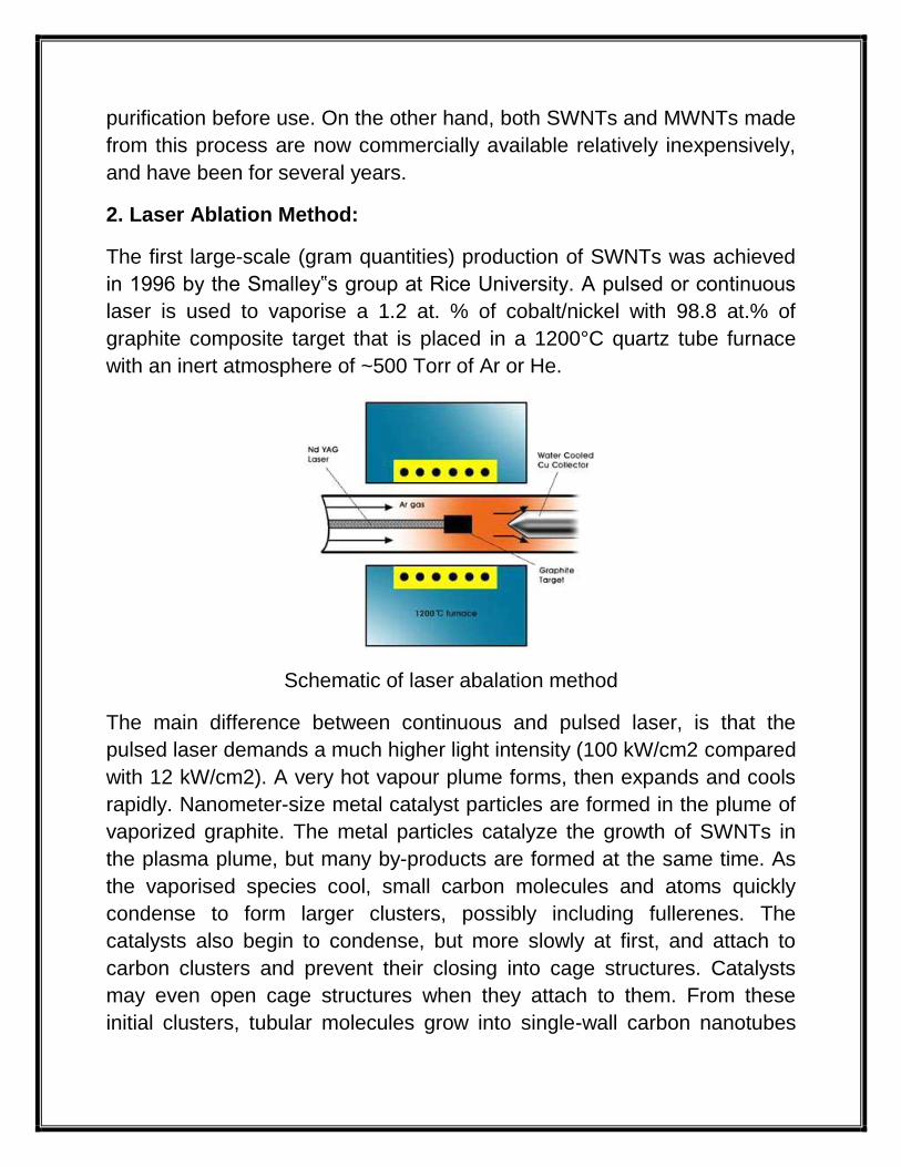
2. Laser Ablation Method:
The first large-scale (gram quantities) production of SWNTs was achieved
in 1996 by the Smalley‟s group at Rice University. A pulsed or continuous
laser is used to vaporise a 1.2 at. % of cobalt/nickel with 98.8 at.% of
graphite composite target that is placed in a 1200°C quartz tube furnace
with an inert atmosphere of ~500 Torr of Ar or He.
Schematic of laser abalation method
The main difference between continuous and pulsed laser, is that the
pulsed laser demands a much higher light intensity (100 kW/cm2 compared
with 12 kW/cm2). A very hot vapour plume forms, then expands and cools
rapidly. Nanometer-size metal catalyst particles are formed in the plume of
vaporized graphite. The metal particles catalyze the growth of SWNTs in
the plasma plume, but many by-products are formed at the same time. As
the vaporised species cool, small carbon molecules and atoms quickly
condense to form larger clusters, possibly including fullerenes. The
catalysts also begin to condense, but more slowly at first, and attach to
carbon clusters and prevent their closing into cage structures. Catalysts
may even open cage structures when they attach to them. From these
initial clusters, tubular molecules grow into single-wall carbon nanotubes

until the catalyst particles become too large, or until conditions have cooled
sufficiently that carbon no longer can diffuse through or over the surface of
the catalyst particles. It is also possible that the particles become that much
coated with a carbon layer that they cannot absorb more and the nanotube
stops growing.
The SWNTs formed in this case are bundled together by van der Waals
forces. The nanotubes and by-products are collected via condensation on a
cold finger downstream from the target. The yield varies from 20 to 80% of
SWNTs by weight. The by-products of this synthesis are graphitic and
amorphous carbon, ―bucky onions‖ (concentric fulleriod spheres)
surrounding metal catalyst particles and small fullerenes (C60, C70, etc.).
In principle, arc discharge and laser ablation are similar methods, as both
use a metal-impregnated graphite target (anode) to produce SWNTs, and
both produce MWNT and fullerenes when pure graphite is used instead.
However, the length of MWNT produced through laser ablation is much
shorter than that produced by arc discharge method. Therefore, this
method does not seem adequate for the synthesis of MWNT.The diameter
distribution of SWNTs made by this method is roughly between 1.0 and 1.6
nm. Because of the good quality of nano tubes produced by this method,
scientist are trying to scale up laser abalation method.
(b) Thermal Synthesis Process:-
Arc discharge and laser ablation methods are fundamentally plasma based
synthesis. However, in thermal synthesis, only thermal energy is relied and
the hot zone of reaction never goes beyond 12000C, including the case of
plasma enhanced CVD. In almost all cases, in presence of active catalytic
species such as Fe, Ni, and Co, carbon feedstock produces CNTs.
Depending on the carbon feedstock, Mo and Ru are sometimes added as
promoters to render the feedstock more active for the formation of CNTs. In
fact, thermal synthesis is a more generic term to represent various
chemical vapor deposition methods. It includes Chemical Vapor Deposition
processes, Carbon monoxide synthesis processes and flame synthesis.

i. Chemical Vapor Deposition:
Chemical vapour deposition (CVD) synthesis is achieved by putting a
carbon source in the gas phase and using energy source to transfer energy
to a gaseous carbon molecule. The CVD process encompasses a wide
range of synthesis techniques, from the gram-quantity bulk formation of
nanotube material to the formation of individual aligned SWNTs on SiO2
substrates for use in electronics.
CVD can also produce aligned vertical MWNTs for use as high-
performance field emitters. Commonly used gaseous carbon sources
include methane, carbon monoxide and acetylene. The energy source is
used to ―crack‖ the molecule into reactive atomic carbon. Then, the carbon
diffuses towards the substrate, which is heated and coated with a catalyst
where it will bind. The catalysts usually used are first row transition metals
such as Ni, Fe or Co. Carbon nanotubes will be formed if the proper
parameters are maintained. Excellent alignment, as well as positional
control on nanometer scale, can be achieved by using CVD. Control over
the diameter, as well as the growth rate of the nanotubes can also be
maintained. The appropriate metal catalyst can preferentially grow single
rather than multi-walled nanotubes.
Schematic of CVD Process
CVD carbon nanotube synthesis is essentially a two-step process
consisting of a catalyst preparation step followed by the actual synthesis of
the nanotube. The catalyst is generally prepared by sputtering a transition
metal onto a substrate and then using either chemical etching or thermal
annealing to induce catalyst particle nucleation. Thermal annealing results
in cluster formation on the substrate, from which the nanotubes will grow.
Ammonia may be used as the etchant. The temperatures for the synthesis

of nanotubes by CVD are generally within the 550-1200 0C range.
CVD in its various forms produces SWNT material of higher atomic quality
and higher percent yield than the other methods currently available and, as
such, represents a significant advance in SWNT production. The majority of
SWNT production methods developed lately such as plasma enhanced
CVD, thermal chemical CVD, alcohol catalytic CVD, vapour phase growth,
aero gel-supported CVD and laser assisted CVD have been direct
descendents of basic CVD.
Simply put, gaseous carbon feedstock is flowed over transition metal
nanoparticles at medium to high temperature and reacts with the
nanoparticles to produce SWNTs. With CVD SWNTs anywhere from 0.4 to
5 nm can be readily produced and depending on the conditions, feedstock,
and catalyst, the yield can exceed 99% (weight percent of final material)
and the final product can be completely free of amorphous carbon.
ii. Plasma Enhanced CVD (PECVD):
Plasma-enhanced chemical vapor deposition (PECVD) systems have been
used to produce both SWNTs and MWNTs. PECVD is a general term,
encompassing several differing synthesis methods. In general PECVD can
be direct or remote. Direct PECVD systems can be used for the production
of MWNT field emitter towers and some SWNTs (Figure 4). A remote
PECVD can also be used to produce both MWNTs and SWNTs (Figure 5).
For SWNT synthesis in the direct PECVD system, the researchers heated
the substrate up to 550 to 850°C, utilized a CH4/H2 gas mixture at 500 mT,
and applied 900 W of plasma power as well as an externally applied
magnetic field. The remote PECVD system utilized by Li et al. used CH4/Ar
held at 500 mT, with only 50 to 75 W of plasma power.
The plasma enhanced CVD method generates a glow discharge in a
chamber or a reaction furnace by a high frequency voltage applied to both
electrodes. A substrate is placed on the grounded electrode. In order to
form a uniform film, the reaction gas is supplied from the opposite plate.
Catalytic metal, such as Fe, Ni and Co are used on a Si, SiO2, or glass
substrate using thermal CVD or sputtering.

Schematic of PECVD
After nanoscopic fine metal particles are formed, carbon nanotubes will be
grown on the metal particles on the substrate by glow discharge generated
from high frequency power. A carbon containing reaction gas, such as
C2H2, CH4, C2H4, C2H6, CO is supplied to the chamber during the
discharge.
To grow SWNT by hot-wire CVD (HWCVD), hydrocarbons with dissolved
Fe-containing molecules are passed over an extremely hot filament near
the furnace entrance to facilitate a plasma-induced breakdown of
hydrocarbons and nucleation of nanotube growth. By initiating growth in the
vapor phase, a substrate can be placed downstream in a cooler area of the
furnace (~450°C) so that the nanotubes can deposit from the vapor phase
onto the substrate. This is useful because by lowering the substrate
temperature, the variety of substrates on which SWNTs can be synthesized
is widened.
Schematic of HWCVD

As such, PECVD and HWCVD is essentially a crossover between plasma-
based growth and CVD synthesis. In contrast to arc discharge, laser
ablation, and solar furnace, the carbon for PECVD synthesis comes from
feedstock gases such as CH4 and CO, so there is no need for a solid
graphite source. The argon-assisted plasma is used to break down the
feedstock gases into C2, CH, and other reactive carbon species (CxHy) to
facilitate growth at low temperature and pressure.
The growth of vertically aligned carbon nanotubes using Ni catalyst layer in
PECVD process has been observed. The growth properties are studied as
a function of the Ni catalyst layer thickness, bias voltage, deposition
temperature, C2H2:NH3 ratio, and pressure. It was found that the diameter,
growth rate, and areal density of the nanotubes are controlled by the initial
thickness of the catalyst layer. The alignment of the nanotubes depends on
the electric field. It has been found that the growth occurs by diffusion of
carbon through the Ni catalyst particle, which rides on the top of the
growing tube. The catalyst has a strong effect on the nanotube diameter,
growth rate, wall thickness, morphology and microstructure. Ni seems to be
the most suitable pure-metal catalyst for the growth of aligned multiwalled
carbon nanotubes (MWNTs). The diameter of the MWNTs is approximately
15 nm. The highest yield of carbon nanotubes achieved was about 50%
and was obtained at relatively low temperatures as below as 330 0C.
(c) Ball Milling:- Ball milling and subsequent annealing is a simple method for the production of CNTs. Although it is well established that mechanical attrition of this type can lead to fully nano porous microstructures, it was not until a few years ago that CNTs of carbon and boron nitride were produced from these powders by thermal annealing. Essentially the method consists of placing graphite powder into a stainless steel container along with four hardened steel balls. The container is purged, and argon is introduced. The milling is carried out at room temperature for up to 150 hours. Following milling, the powder is annealed under an inert gas flow at temperatures of 1400°C for six hours. The mechanism of this process is not known, but it is thought that the ball milling process forms nanotube nuclei, and the annealing process activates nanotube growth. Research has shown that
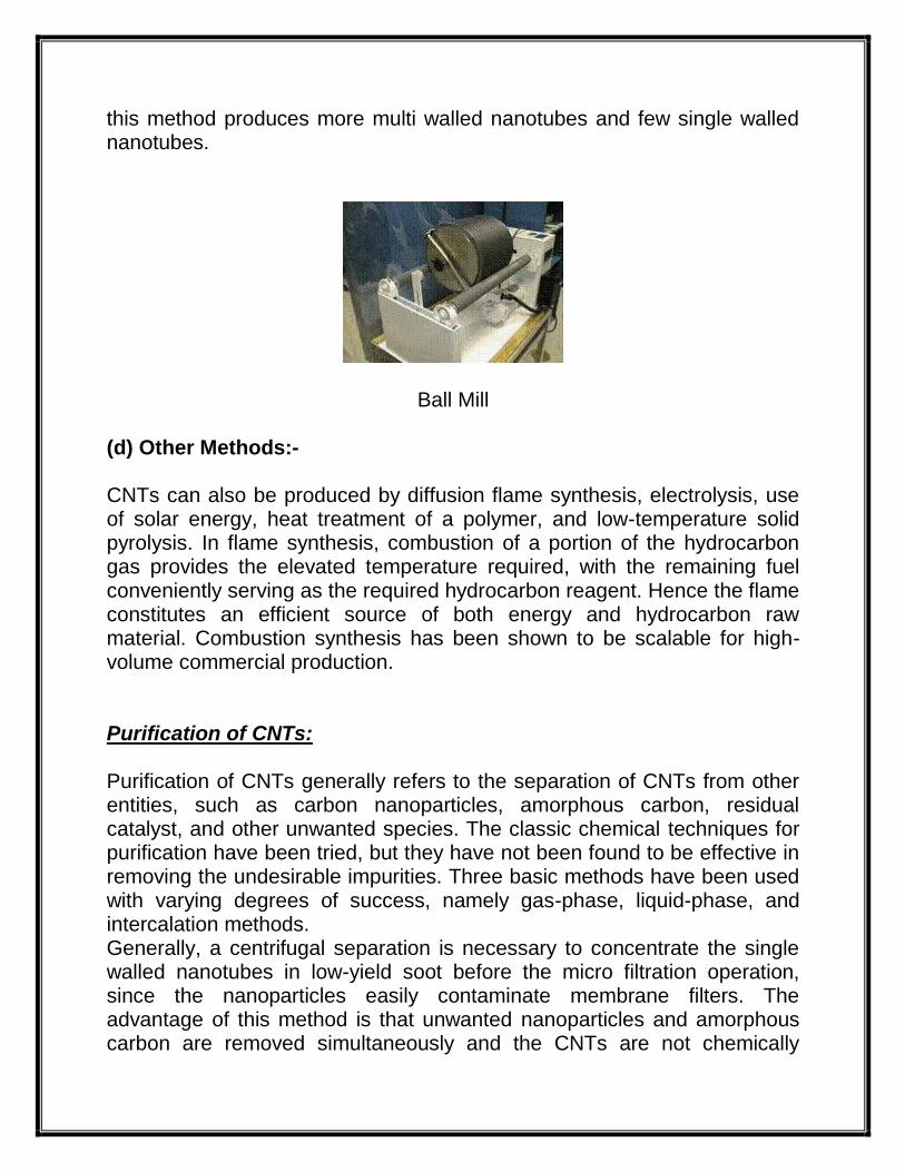
this method produces more multi walled nanotubes and few single walled nanotubes.
Ball Mill (d) Other Methods:- CNTs can also be produced by diffusion flame synthesis, electrolysis, use of solar energy, heat treatment of a polymer, and low-temperature solid pyrolysis. In flame synthesis, combustion of a portion of the hydrocarbon gas provides the elevated temperature required, with the remaining fuel conveniently serving as the required hydrocarbon reagent. Hence the flame constitutes an efficient source of both energy and hydrocarbon raw material. Combustion synthesis has been shown to be scalable for high-volume commercial production. Purification of CNTs: Purification of CNTs generally refers to the separation of CNTs from other entities, such as carbon nanoparticles, amorphous carbon, residual catalyst, and other unwanted species. The classic chemical techniques for purification have been tried, but they have not been found to be effective in removing the undesirable impurities. Three basic methods have been used with varying degrees of success, namely gas-phase, liquid-phase, and intercalation methods. Generally, a centrifugal separation is necessary to concentrate the single walled nanotubes in low-yield soot before the micro filtration operation, since the nanoparticles easily contaminate membrane filters. The advantage of this method is that unwanted nanoparticles and amorphous carbon are removed simultaneously and the CNTs are not chemically

modified. However 2-3 mol nitric acid is useful for chemically removing impurities. It is now possible to cut CNTs into smaller segments, by extended sonication in concentrated acid mixtures. The resulting CNTs form a colloidal suspension in solvents. They can be deposited on substrates, or further manipulated in solution, and can have many different functional groups attached to the ends and sides of the CNTs.
(a) Gas Phase
The first successful technique for purification of nanotubes was developed by Thomas Ebbesen and coworkers. Following the demonstration that nanotubes could be selectively attached by oxidizing gases these workers realized that nanoparticles, with their defect rich structures might be oxidised more readily than the relatively perfect nanotubes. They found that a significant relative enrichment of nanotubes could be achieved this way, but only at the expense of losing the majority of the original sample. A new gas-phase method has been developed at the NASA Glenn Research Center to purify gram-scale quantities of single-wall CNTs. This method, a modification of a gas-phase purification technique previously reported by Smalley and others, uses a combination of high-temperature oxidations and repeated extractions with nitric and hydrochloric acid. This improved procedure significantly reduces the amount of impurities such as residual catalyst, and non-nanotube forms of carbon) within the CNTs, increasing their stability significantly.
(b) Liquid Phase
The current liquid-phase purification procedure follows certain essential steps: preliminary filtration- to get rid of large graphite particles; dissolution- to remove fullerenes (in organic solvents) and catalyst particles (in concentrated acids) centrifugal separation- microfiltration- and chromatography
It is important to keep the CNTs well-separated in solution, so the CNTs are typically dispersed using a surfactant prior to the last stage of separation.
(c) Intercalation
An alternative approach to purifying multi walled nanotubes was introduced in 1994 by a Japanese research group. This technique made use of the fact that nanoparticles and other graphitic contaminants have relatively ―open‖ structures and can therefore be more readily intercalated with a variety of materials that can close nanotubes. By intercalating with copper chloride, and then reducing this to metallic copper, the research group was able to preferentially oxidize the nanoparticles away, using copper as an oxidation catalyst. Since 1994, this has become a popular method for purification of nanotubes. ―The first stage is to immerse the crude cathodic deposit in a molten copper chloride and potassium chloride mixture at 400°C and leave it for one week. The product of this treatment, which contains intercalated nanoparticles and graphitic fragments, is then washed in ion exchanged water to remove excess copper chloride and potassium chloride. In order to reduce the intercalated copper chloride-potassium chloride metal, the washed product is slowly heated to 500°C in a mixture of Helium and hydrogen and held at this temperature for 1 hour. Finally, the material is oxidized in flowing air at a rate of 10°C/min to a temperature of 555°C. Samples of cathodic soot which have been treated this way consist almost entirely of nanotubes. A disadvantage of this method is that some amount of nanotubes are inevitably lost in the oxidation stage, and the final material may be contaminated with residues of intercalates. A similar purification technique, which involves intercalation with bromine followed by oxidation, has also been described. Functionalization:- Pristine nanotubes are unfortunately insoluble in many liquids such as water, polymer resins, and most solvents. Thus they are difficult to evenly disperse in a liquid matrix such as epoxies and other polymers. This complicates efforts to utilize the nanotubes’ outstanding physical properties in the manufacture of composite materials, as well as in other practical

applications which require preparation of uniform mixtures of CNTs with many different organic, inorganic, and polymeric materials. To make nanotubes more easily dispersible in liquids, it is necessary to physically or chemically attach certain molecules, or functional groups, to their smooth sidewalls without significantly changing the nanotubes’ desirable properties. This process is called functionalization. The production of robust composite materials requires strong covalent chemical bonding between the filler particles and the polymer matrix, rather than the much weaker van der Waals physical bonds which occur if the CNTs are not properly functionalized. Functionalization methods such as chopping, oxidation, and ―wrapping‖ of the CNTs in certain polymers can create more active bonding sites on the surface of the nanotubes. For biological uses, CNTs can be functionalized by attaching biological molecules, such as lipids, proteins, biotins, etc. to them. Then they can usefully mimic certain biological functions, such as protein adsorption, and bind to DNA and drug molecules. This would enable medially and commercially significant applications such as gene therapy and drug delivery. In biochemical and chemical applications such as the development of very specific biosensors, molecules such as carboxylic acid (COOH), poly m-aminobenzoic sulfonic acid (PABS), polyimide, and polyvinyl alcohol (PVA) have been used to functionalize CNTs, as have amino acid derivatives, halogens, and compounds. Some types of functionalized CNTs are soluble in water and other highly polar, aqueous solvents.
Applications of CNTs:-
1.Conductive or reinforced plastics:
Much of the history of plastics over the last half-century has involved their use as a replacement for metals. For structural applications, plastics have made tremendous headway, but not where electrical conductivity is
required, because plastics are very good electrical insulators. This deficiency is overcome by loading plastics up with conductive fillers, such as carbon black and larger graphite fibers. The loading required to provide the necessary conductivity using conventional fillers is typically high, however, resulting in heavy parts, and more importantly, plastic parts whose structural properties are highly degraded. It is well-established that the higher the aspect ratio of the filler particles, the lower the loading required to achieve a given level of conductivity. CNTs are ideal in this sense, since they have the highest aspect ratio of any carbon fiber. In addition, their natural tendency to form ropes provides inherently very long conductive pathways even at ultra-low loadings. Applications that exploit this behavior of CNTs include EMI/RFI shielding composites; coatings for enclosures, gaskets, and other uses such as electrostatic dissipation; antistatic materials, transparent conductive coatings; and radar-absorbing materials for stealth applications. A lot of automotive plastics companies are using CNTs as well. CNTs have been added into the side mirror plastics on automobiles in the US since the late 1990s. I have seen forecasts predicting that GM alone will consume over 500 pounds of CNT masterbatches in 2006 for using in all areas of automotive plastics. Masterbatches normally contain 20 wt% cnts which are already very well dispersed. Manufacturers then need to perform a ―let down‖ or dilution procedure prior to using the masterbatch in production.
2.Energy storage:
CNTs have the intrinsic characteristics desired in material used as electrodes in batteries and capacitors, two technologies of rapidly increasing importance. CNTs have a tremendously high surface area, good electrical conductivity, and very importantly, their linear geometry makes their surface highly accessible to the electrolyte. Research has shown that CNTs have the highest reversible capacity of any carbon material for use in lithium ion batteries. In addition, CNTs are outstanding materials for super capacitor electrodes and are now being marketed for this application. CNTs also have applications in a variety of fuel cell components. They have a number of properties, including high surface area and thermal conductivity, which make them useful as electrode catalyst supports in PEM fuel cells. Because of their high electrical conductivity, they may also be used in gas diffusion layers, as well as current collectors. CNTs' high strength and toughness-to-weight characteristics may also prove valuable as part of composite components

in fuel cells that are deployed in transport applications, where durability is extremely important.
3. Conductive adhesives and connectors:
The same properties that make CNTs attractive as conductive fillers for use in electromagnetic shielding, ESD materials, etc., make them attractive for electronics packaging and interconnection applications, such as adhesives, potting compounds, coaxial cables, and other types of connectors.
4. Carbon Nanotubes in Electronics:
It should be pointed out that the integration of nanotubes into electronic
devices still is a long-term application with the prospect of commercial
products beyond the ten-year time frame. However, nanotubes (in
particular, SWNTs) have emerged as a promising class of electronic
materials due to their nanoscale dimensions and outstanding properties,
such as ballistic electronic conduction and insensitivity to electromigration .
Both metallic and semiconducting SWNTs are found to possess electrical
characteristics that compare favorably with the best electronic materials
presently available. The recent advances in the separation of SWNTs with
different electronic properties has enabled the nanotube community to
develop the field-effect transistors (FET) and interconnects on a large
scale.
In hot pursuit of Moore’s law, semiconductor giants like Intel, IBM, AMD,
UMC and TSMC are commercially manufacturing silicon-based transistors
at the 65-nm technology node. Intel intends to commercialize transistors at
the 45-nm technology node by the end of 2007 or early 2008. By an
evolutionary process, a conservative estimate for the smallest conceivable
silicon transistor at this point is 16 nm, expected to hit markets not prior to
2018. A revolutionary speedup of this process can be realistically
envisioned only if nanotechnology can be controlled on a large scale.
Single-wall carbon nanotubes, with a diameter of ∼ 1 nm, have been
demonstrated to operate as field-effect transistors almost a decade ago,
and since then, the FETs have steadily grown in versatility and promise for

future nanometer scale electronics.
Nano transistors
5. Molecular electronics:
The idea of building electronic circuits out of the essential building blocks of materials - molecules - has seen a revival the past few years, and is a key component of nanotechnology. In any electronic circuit, but particularly as dimensions shrink to the nanoscale, the interconnections between switches and other active devices become increasingly important. Their geometry, electrical conductivity, and ability to be precisely derived, make CNTs the ideal candidates for the connections in molecular electronics. In addition, they have been demonstrated as switches themselves. There are already companies such as Nantero from Woburn, MA that are already making CNT based non-volitle random access memory for PC’s. A lot of research is being done to design CNT based transistors as well. 6. Thermal materials: The record-setting anisotropic thermal conductivity of CNTs is enabling many applications where heat needs to move from one place to another. Such an application is found in electronics, particularly heat sinks for chips used in advanced computing, where uncooled chips now routinely reach over 100oC. The technology for creating aligned structures and ribbons of CNTs [D.Walters, et al., Chem. Phys. Lett. 338, 14 (2001)] is a step toward realizing incredibly efficient heat conduits. In addition, composites with CNTs have been shown to dramatically increase their bulk thermal conductivity, even at very small loadings.

7. Structural composites: The superior properties of CNTs are not limited to electrical and thermal conductivities, but also include mechanical properties, such as stiffness, toughness, and strength. These properties lead to a wealth of applications exploiting them, including advanced composites requiring high values of one or more of these properties.
8. Fibers and fabrics:
Fibers spun of pure CNTs have recently been demonstrated and are
undergoing rapid development, along with CNT composite fibers. Such
super-strong fibers will have many applications including body and vehicle
armor, transmission line cables, woven fabrics and textiles.
9. Catalyst support:
CNTs intrinsically have an enormously high surface area; in fact, for single
walled nanotubes every atom is not just on one surface - each atom is on
two surfaces, the inside and the outside of the nanotube! Combined with
the ability to attach essentially any chemical species to their sidewalls this
provides an opportunity for unique catalyst supports. Their electrical
conductivity may also be exploited in the search for new catalysts and
catalytic behavior.
10. CNT Ceramics:
A ceramic material reinforced with carbon nanotubes has been made by materials scientists at UC Davis. The new material is far tougher than conventional ceramics, conducts electricity and can both conduct heat and act as a thermal barrier, depending on the orientation of the nanotubes. Ceramic materials are very hard and resistant to heat and chemical attack, making them useful for applications such as coating turbine blades, but they are also very brittle. The researchers mixed powdered alumina (aluminum oxide) with 5 to 10 percent carbon nanotubes and a further 5 percent finely milled niobium. The researchers treated the mixture with an electrical pulse in a process called spark-plasma sintering. This process consolidates ceramic powders more quickly and at lower temperatures than conventional processes.

The new material has up to five times the fracture toughness -- resistance to cracking under stress -- of conventional alumina. The material shows electrical conductivity seven times that of previous ceramics made with nanotubes. It also has interesting thermal properties, conducting heat in one direction, along the alignment of the nanotubes, but reflecting heat at right angles to the nanotubes, making it an attractive material for thermal barrier coatings. 11. Air, water and gas filtration: Many researchers and corporations have already developed CNT based air and water filtration devices. It has been reported that these filters can not only block the smallest particles but also kill most bacteria. This is another area where CNTs have already been commercialized and products are on the market now. Someday CNTs may be used to filter other liquids such as fuels and lubricants as well. A lot of research is being done in the development of CNT based air and gas filtration. Filtration has been shown to be another area where it is cost effective to use CNTs already. The research I’ve seen suggests that 1 gram of MWNTs can be dispersed onto 1 sq ft of filter media. Manufacturers can get their cost down to 35 cents per gram of purified MWNTs when purchasing ton quantities.
12. Field Emission Displays:
Flat-panel field-emission display using CNT electron source provides a
high-brightness display for both consumer and professional applications.
The function of a simplest display is shown in figure. Nanotubes are
patterned on a matrix of electrodes in a vacuum housing. The counter
electrode is a glass plate (can use ITO glass) coated with a conducting but
transparent layer and a phosphor layer. A voltage difference of a few
kilovolts between the nanotube cathode and the glass plate results in field
emission and the generation of light through excitation of the
cathodoluminescent phosphor. An image can be obtained by addressing
selectively the different positions of the matrix, which can either be
monochrome or in colour (if each pixel is divided in red, blue and green
sub-pixels).

The charging effect at the isolating spacers between the cathode and
anode is one of the problems yet to be solved. The difficulty to operate with
a large voltage between cathode and anode is another problem. It can be
addressed by using a gate electrode to control the emission with the gate-
to-cathode voltage. The arrangement is shown in fig.1(b). Gate can also be
used to converge the electron beam so that higher brightness and a
sharper image can be obtained. The electron beam spreads out in space
and the direction of the beam varies from nanotube to nanotube.So the
ideal condition of „one emitting pixel addresses only one pixel on the
screen‟ can not be achieved.
Schematic of working principle of field emission display pixels
(a)Diode structure
(b)Triode structure with ballast resistor in series with emitters
13. CNT Based Sensors for Various Applications:
Gas sensors are a omnipresent part of our everyday lives. Various types of
gas sensors are present in automobiles, commercial and industrial
buildings, and even in many homes. The purpose of these sensors varies
depending on their application. Automotive gas sensors enable a motor
vehicle to operate cleanly and efficiently. Commercial and industrial gas

sensors help ensure employees are not exposed to harmful toxins in the
workplace. Gas sensors in the home primarily protect families from the
deadly effects of carbon monoxide poisoning.
Gas sensors with high sensitivity and selectivity are required for leakage
detections of explosive gases such as hydrogen, and for real-time
detections of toxic or pathogenic gases in industries.
There is also a strong demand for the ability to monitor and control our
ambient environment, especially with the increasing concern of the globe
warming. Researchers from the national aeronautics and space
administration (NASA) are seeking the use of high-performance gas
sensors for the identification of atmospheric components of various planets.
In addition, nerve agent sensing for homeland security is also at the centre
of public concern.
CNT Based Gas Sensor
Generally, there are several basic criteria for good and efficient gas
sensing systems:
(i) high sensitivity and selectivity;
(ii) fast response time and recovery time;
(iii) low analyst consumption;

(iv) low operating temperature and temperature independence;
(v) stability in performances.
Commonly used gas sensing materials include vapour-sensitive polymers,
semiconductor metal oxides, and other porous structured materials such as
porous silicon. Since the most common gas sensing principle is the
adsorption and desorption of gas molecules on sensing materials, it is quite
understandable that by increasing the contact interfaces between the
analytes and sensing materials, the sensitivity can be significantly
enhanced.
Recent development of nanotechnology has created huge potential to build
highly sensitive, low cost, portable sensors with low power consumption.
The extremely high surface-to-volume ratio and hollow structure of
nanomaterials is ideal for gas molecules adsorption and storage.
Therefore, gas sensors based on nanomaterials, such as carbon
nanotubes (CNTs), nanowires, nanofibers, and nanoparticles, have been
used widely.
14. Multi Walled Carbon Nanotube based Gas Sensor for NH3:
Multi-walled carbon nanotube (MWNT) based gas sensors for detecting
gaseous molecules of ammonia (NH3) were developed. It is found that the
conductance of MWNTs decreases when the sensors successively
exposed to NH3 gas at room temperature of 25 °C. The MWNT-based
sensors are sensitive to NH3 gas. This suggests that the MWNTs could be
a good candidate material for NH3 detection at room temperature.
15. Single Walled Carbon Nanotube based Gas Sensor for NO2 :
The sensitivity of the SWNT monolayer network-based sensors to NO2 gas
was investigated at room temperature by Department of Physics and
Astronomy. They have found that the response of the gas sensors is
inversely proportional to the initial conductance of the SWNT network. This
behavior is different from conventional gas sensors based on uniform films,
and it may be critical for the calibration of sensors in practical applications.

16. CNT Sensor Array for Various Gas Detection:
A carbon nanotube based gas sensor array was developed for
discriminating gases and vapors by Center for Nanotechnology, NASA
Ames Research Center, United States. The sensor array was composed of
32 sensing elements with nano materials, e.g. pristine single walled carbon
nanotubes (SWNTs), and SWNTs with different metal dopants and polymer
coatings. This sensor array was exposed to NO2, HCN, HCl, Cl2, acetone
and benzene in parts per million (ppm) concentration levels. All tested
gases and vapors can be discriminated by their chemical nature in the low
gas/vapor concentration at ppm levels using this carbon nanotube based
sensor array.
Gas Sensors
17. Carbon Nanotubes in Drug Delivery:
The development of new and efficient drug delivery systems is of
fundamental importance to improve the pharmacological profiles of many
classes of therapeutic molecules. Many different types of drug delivery
systems are currently available. Within the family of nanomaterials, carbon
nanotubes (CNT) have emerged as a new alternative and efficient tool for
transporting and translocating therapeutic molecules. CNT can be
functionalised with bioactive peptides, proteins, nucleic acids and drugs,
and used to deliver their cargos to cells and organs. Because

functionalized CNT display low toxicity and are not immunogenic, such
systems hold great potential in the field of nano biotechnology and
nanomedicine.
(a) Carbon Nano Tube in drug delivery (b)Gold NPs in controlled
drug delivery
One of the most impressive and potentially life changing potential for the use of nanotubes is the ability to help the human body transmit nerve signals where there was previous damage.
When the spinal cord receive trauma, the brain and the body are often cut off from each other by the lack of nerve signal transmission along the spinal cord. Nanotubes have actually been proven to be able to correct this problem in some patients.
Nanotubes are actuall stronger than steel by about one hundred times. Additionally, nanotubes are a fantastic electricity conductor, outperforming copper and silicone.
When nanotubes are used as semiconductor chips their potential is actually limitless. Their strength and their ability to conduct electricity make them prime options for medical advancement, space exploration, undersea exploration, and even computer advancement. The carbon nanotube could one day become the basis of all sciences.
Medical science has been able to see the potential for medical advancement. Paralysis and neurological diseases could be treated and even cured with the nanotube. Once carbon nanotubes are created for nerve cell transmission, the potential for human cell growth on the surface makes nanotube therapies a prime choice for all of medical science to continue to explore.

There is promising research that indicates that the cure for cancer could lay in the hands of nanoscience. Since the nanotubes’ surfaces allow for the growth of human cells, the hope is that the nanotubes could be injected into cancer patients with pinpoint accuracy and the cancer cells could be destroyed while noncancerous cells would be encouraged to grow on the nanotubes’ surfaces.
This technology has not been perfected yet but the hope that the technology will one day eradicate cancer. This hope is thus far the most promising that medical science has ever witnessed.
Those who suffer from diseases and ailments like chronic pain, Parkinson’s disease, and even depression may very well also be helped by the use of nanotubes. By creating the nanotubes to conduct specific nerve impulses, the altered nerve impulses that can cause the symptoms of these diseases can be over ridden.
Those who are opposed to stem cell research believe often have cited that there has been drastic improvements in the research that nanotubes present. It could have the same effect with the ability to engineer them for specific nerve cell signals.
We have the technology to direct the nanotubes to respond to human cells in different ways, which would allow us to direct the nanotubes to address diseases on the cellular level. The potential to treat almost any disease exists with the use of nanotubes.
Nanotube research is not as well-known as other forms of medical research, but it holds great promise. It is vital that the communities that will one day implement this science continue to increase their education regarding nanotechnology and all possible applications of nanotubes.
Nanotubes are now being coated to increase their ability to respond to nerve cell direction, they are being tested on human cancer cells and even worms.
They are being specifically created for various disease relief. While the science and the technology has not received much media attention (most likely because it is not controversial) there are some human trials taking place around the world to attempt to prove that this is the next viable treatment options for many medical problems.
18. Other applications:
Some commercial products on the market today utilizing CNTs include
stain resistant textiles, CNT reinforced tennis rackets and baseball bats.
Companies like Kraft foods are heavily funding cnt based plastic
packaging. Food will stay fresh longer if the packaging is less permeable to
atmosphere. Coors Brewing company has developed new plastic beer
bottles that stay cold for longer periods of time. Samsung already has CNT
based flat panel displays on the market. A lot of companies are looking
forward to being able to produce transparent conductive coatings and
phase out ITO coatings. Samsung uses align SWNTs in the transparent
conductive layer of their display manufacturing process.
Carbon Nanotube Biofuels:
Carbon nanotubes are widely popular and widely debated in scientific and research circles because they are feather light, stronger than many other materials—especially stronger than most man-made materials, and because they have some toxic properties in addition to their uniquely useful properties.
Carbon nanotubes have the ability to change architecture, the automobile industry, materials science, the space program and a variety of activities and products associated with daily living. These nanotubes are able to be produced on industrial mass scales and the commercial production of carbon nanotubes through synthesis make them incredibly affordable, costing as little as 95 dollars per gram at present—with the price going down every year—making them a uniquely affordable in the creation of carbon nanotubes biofuel.
At present, many different studies are being performed all over the world to deduce the use of nanotubes in the production of carbon nanotubes biofuel. These studies are using a variety of different biological matter including glucose, hydroxyapatite, porous silicon and even vegetables such as corn and tomato plants. The most popular studies for this biofuel and

other implications in agriculture are the Glucose Oxidase studies and those studies involving the use of growing plants, like tomatoes.
Biofuel cells are an increasingly popular topic for study, experiment and research in the scientific fields, partially due to the constantly depleting sources of fossil fuels on the planet and also due to the fact that biofuels, unlike fossil fuels, are a completely renewable resource.
As long as plants and other biological materials can grow, and grow quickly, biofuels will prove to be a much cheaper and easier alternative for the world. Fossil fuels, on the other hand, while renewable, took hundreds of thousands of years to become what they are today and required incredible circumstances to synthesize that do not all exist today. Most biofuels are made with Glucose Oxidase although many are made with other enzymes or even microorganisms.
Carbon nanotubes biofuels are growing in popularity amongst scientists and researches because these biofuels are much stronger than any of those previously studied or created. Because of the unique construction of carbon nanotubes, the carbon nanotubes biofuels that are presently being created are unlike any other biofuel in existence. They may have implications for all present uses of biofuels including, alternative fuel source vehicles, pacemakers, portable energy supplies and even glucose sensors.
When carbon nanotubes are used in junction with glucose oxidase to produce carbon nanotubes biofuel, the carbon nanotubes form a covalent bond with the glucose oxidase, creating a biofuel that is not only stronger than traditional biofuels but that also has a high electrical output, making these new biofuels useful for a large number of applications across the practical field of sciences, materials science and even modern day living.
What is more interesting at present is the use of carbon nanotubes in increasing the growth in size, quantity and speed, of vegetables like tomatoes. In September 2009, a team of researchers at the Little Rock Nanotechnology Center, housed at the University of Arkansas, used carbon nanotubes to increase the germination rate of tomato plants.
In addition, this exposure caused the seedlings to become stronger and grow more quickly. What the carbon nanotubes did for the plants in this study was to become a part of the seed by penetrating through the thick outer shell and bonding with the plant structure.

This in turn made it possible for the plants not only to take in more water, but to hold that water, creating a plant that could possibly survive a longer drought period after a long rain fall. Interestingly, although not related to its properties as a biofuel in this instance, the effects the carbon nanotubes had on these plants seemed to make them toxic to fruit flies.
The effects and outcomes of this particular study point to carbon nanotubes biofuel as the wave of the future. If carbon nanotubes are able to create stronger, better and more quickly growing plants, their implications for agriculture, especially in terms of creating biofuels, are greater than most scientists could ever have imagined.
However, even as carbon nanotubes biofuel becomes more of a reality rather than a possibility for the far off future, there are many implications to consider. If carbon nanotubes are toxic to fruit flies, what might their implications be for human beings? Additionally, it has been reported that wastes from this type of biofuel may have been a factor in the cause of asbestos and other carcinogens in the lungs of some mice. The toxic properties and possibilities that come with carbon nanotubes biofuel should be taken into account.
The purpose of using biofuels in our modern world is to help eliminate the dangers that come with fossil fuels. Fossil fuels are damaging the ozone and difficult and expensive to extract and make usable. At this point in time, it seems that while carbon nanotubes biofuels may be less expensive to produce on a mass scale, they are currently as dangerous, if not more so, for animals, humans and the earth than fossil fuels.
Research will continue into the development of carbon nanotubes for use in biofuels and other agricultural pursuits and we can only hope that solutions to the toxic properties are discovered long before these biofuels are put into mass production for public and commercial use.

Conclusion:
The unique properties of carbon nano tubes renders its importance in
various fields. Researchers have been looking for cheap synthesis
methods for carbon nano tubes. At present the cheapest method for
production of SWNTs is Arc discharge method and for the production of
MWNTs, is Chemical Vapor Deposition Method. But researchers are still
working on green chemical vapor deposition process which gives less
waste.

References:-
1. Polymer Nanocomposites containing Carbon Nanotubes by
Mohammad Moniruzzaman and Karen I. Winey.
2. High Aspect Ratio Polymer Micro/Nano-Structure Manufacturing using Nanoembossing, Nanomolding and Directed Self-Assembly by Metin Sitti, Dept. of Mechanical Engineering and Robotics Institute,Carnegie Mellon University, Pittsburgh, USA. 3. Electronic Structure of Doped Fullerenes and Single Wall Carbon
Nanotubes by S. Eisebitt, A. Karl, A. Zimina, R. Scherer, M. Freiwald, W. Eberhardt, F. Hauke1, A. Hirsch1, Y. Achiba2.
4. Morphology of Electrospun Nylon-6 Nanofibers as a function of
Molecular Weight and Processing Parameters by Satyajeet S. Ojha,
Mehdi Afshari, Richard Kotek, Russell E. Gorga, Dpt of Fiber and
Polymer Science, College of Textiles, North Carolina State University.
5. Intimate relationship between structural deformation and properties of
single-walled carbon nanotubes and its hydrogenated derivatives by
Taner Yildirim*, Oguz Gulseren and Salim Ciraci**,* NIST Center for
Neutron Research, Gaithersburg, MD 20899, USA; **Physics
Department, Bilkent University, 06533, Ankara, Turkey.
6. http://nanogloss.com/
7. http://www.nanowerk.com
8. http://nstc.celnet.in/
9. Wikipedia.

Declaration: I, hereby, declare that the contents above are correct to the best of my knowledge. I transfer the copyright of this document to NSTC.
(Ronika Goswami)
Chemical Engineering
VNIT, Nagpur