car alternator multifunction smart voltage · pdf filethis is information on a product in full...
TRANSCRIPT

This is information on a product in full production.
September 2015 DocID10990 Rev 13 1/20
L9911
Car alternator multifunction smart voltage regulator
Datasheet - production data
Features Fully monolithic design High side field driver
Thermal protection Field short circuit protection Protected diagnostic lamp driver Protected high side relay driver Complex diagnostics Load response control DFM output (field monitor) Self start function
DescriptionThe L9911 is a monolithic multifunction alternator voltage regulator intended for use in automotive application.
It includes the control section, the field power stage, fault diagnostic circuit which drives a warning lamp, and the protection against short circuits
Multiwatt8
Table 1. Device summaryOrder code Temp. range, °C Package Packing
L9911F
Tj = -40 to +150 Multiwatt8 Tube
L9911I
L9911P
L9911V
L9911K
L9911U
www.st.com

Contents L9911
2/20 DocID10990 Rev 13
Contents
1 Circuit operation . . . . . . . . . . . . . . . . . . . . . . . . . . . . . . . . . . . . . . . . . . . . 51.1 Voltage regulation . . . . . . . . . . . . . . . . . . . . . . . . . . . . . . . . . . . . . . . . . . . . 5
1.2 Protection . . . . . . . . . . . . . . . . . . . . . . . . . . . . . . . . . . . . . . . . . . . . . . . . . . 5
1.3 Diagnosis . . . . . . . . . . . . . . . . . . . . . . . . . . . . . . . . . . . . . . . . . . . . . . . . . . 5
1.4 Load response control . . . . . . . . . . . . . . . . . . . . . . . . . . . . . . . . . . . . . . . . 5
1.5 Self start function . . . . . . . . . . . . . . . . . . . . . . . . . . . . . . . . . . . . . . . . . . . . 5
2 Pin description . . . . . . . . . . . . . . . . . . . . . . . . . . . . . . . . . . . . . . . . . . . . . 6
3 Electrical specification . . . . . . . . . . . . . . . . . . . . . . . . . . . . . . . . . . . . . . . 73.1 Absolute maximum ratings . . . . . . . . . . . . . . . . . . . . . . . . . . . . . . . . . . . . . 7
3.2 Thermal data . . . . . . . . . . . . . . . . . . . . . . . . . . . . . . . . . . . . . . . . . . . . . . . 7
3.3 Electrical characteristics . . . . . . . . . . . . . . . . . . . . . . . . . . . . . . . . . . . . . . . 7
3.4 Principle of phase regulation . . . . . . . . . . . . . . . . . . . . . . . . . . . . . . . . . . 14
4 Package information . . . . . . . . . . . . . . . . . . . . . . . . . . . . . . . . . . . . . . . . 174.1 Multiwatt 8 (pin 5 GND) package information . . . . . . . . . . . . . . . . . . . . . . 17
5 Revision history . . . . . . . . . . . . . . . . . . . . . . . . . . . . . . . . . . . . . . . . . . . 19

DocID10990 Rev 13 3/20
L9911 List of tables
3
List of tables
Table 1. Device summary . . . . . . . . . . . . . . . . . . . . . . . . . . . . . . . . . . . . . . . . . . . . . . . . . . . . . . . . . . 1Table 2. Pin description . . . . . . . . . . . . . . . . . . . . . . . . . . . . . . . . . . . . . . . . . . . . . . . . . . . . . . . . . . . 6Table 3. Absolute maximum ratings . . . . . . . . . . . . . . . . . . . . . . . . . . . . . . . . . . . . . . . . . . . . . . . . . . 7Table 4. Thermal data. . . . . . . . . . . . . . . . . . . . . . . . . . . . . . . . . . . . . . . . . . . . . . . . . . . . . . . . . . . . . 7Table 5. Electrical characteristics . . . . . . . . . . . . . . . . . . . . . . . . . . . . . . . . . . . . . . . . . . . . . . . . . . . . 7Table 6. Load response control parameters . . . . . . . . . . . . . . . . . . . . . . . . . . . . . . . . . . . . . . . . . . . 10Table 7. Load response control timing options . . . . . . . . . . . . . . . . . . . . . . . . . . . . . . . . . . . . . . . . . 10Table 8. Correspondence of frequency (typical values) to application features . . . . . . . . . . . . . . . . 11Table 9. Customization of L9911: combination of LRC, regulation, and application options . . . . . . 11Table 10. Fault detection . . . . . . . . . . . . . . . . . . . . . . . . . . . . . . . . . . . . . . . . . . . . . . . . . . . . . . . . . . 16Table 11. Multiwatt 8 (pin 5GND) package mechanical drawing . . . . . . . . . . . . . . . . . . . . . . . . . . . . 18Table 12. Document revision history. . . . . . . . . . . . . . . . . . . . . . . . . . . . . . . . . . . . . . . . . . . . . . . . . . 19

List of figures L9911
4/20 DocID10990 Rev 13
List of figures
Figure 1. Pin connection (top view) . . . . . . . . . . . . . . . . . . . . . . . . . . . . . . . . . . . . . . . . . . . . . . . . . . . 6Figure 2. Vreg-1. . . . . . . . . . . . . . . . . . . . . . . . . . . . . . . . . . . . . . . . . . . . . . . . . . . . . . . . . . . . . . . . . . 11Figure 3. Vreg-2. . . . . . . . . . . . . . . . . . . . . . . . . . . . . . . . . . . . . . . . . . . . . . . . . . . . . . . . . . . . . . . . . . 12Figure 4. Vreg-3. . . . . . . . . . . . . . . . . . . . . . . . . . . . . . . . . . . . . . . . . . . . . . . . . . . . . . . . . . . . . . . . . . 12Figure 5. Vreg-4. . . . . . . . . . . . . . . . . . . . . . . . . . . . . . . . . . . . . . . . . . . . . . . . . . . . . . . . . . . . . . . . . . 13Figure 6. Output voltage rise/fall time (F+, DFM). . . . . . . . . . . . . . . . . . . . . . . . . . . . . . . . . . . . . . . . 13Figure 7. Phase regulation characteristics . . . . . . . . . . . . . . . . . . . . . . . . . . . . . . . . . . . . . . . . . . . . . 13Figure 8. Application diagram . . . . . . . . . . . . . . . . . . . . . . . . . . . . . . . . . . . . . . . . . . . . . . . . . . . . . . 14Figure 9. High side/low side driver saturation . . . . . . . . . . . . . . . . . . . . . . . . . . . . . . . . . . . . . . . . . . 14Figure 10. Test mode to cancel soft-start/attack . . . . . . . . . . . . . . . . . . . . . . . . . . . . . . . . . . . . . . . . . 14Figure 11. Soft-start enable frequency range . . . . . . . . . . . . . . . . . . . . . . . . . . . . . . . . . . . . . . . . . . . 14Figure 12. Soft-start characteristics (always activated at engine start) . . . . . . . . . . . . . . . . . . . . . . . . 15Figure 13. Soft start/attack characteristics . . . . . . . . . . . . . . . . . . . . . . . . . . . . . . . . . . . . . . . . . . . . . . 15Figure 14. DF monitor electrical configuration . . . . . . . . . . . . . . . . . . . . . . . . . . . . . . . . . . . . . . . . . . . 16Figure 15. Short circuit drivers' protection . . . . . . . . . . . . . . . . . . . . . . . . . . . . . . . . . . . . . . . . . . . . . . 16Figure 16. Multiwatt 8 (pin 5GND) package outline . . . . . . . . . . . . . . . . . . . . . . . . . . . . . . . . . . . . . . . 17

DocID10990 Rev 13 5/20
L9911 Circuit operation
19
1 Circuit operation
The alternator's voltage regulator performs the following main functions:1. voltage regulation2. protection3. control fault diagnosis4. load response control
1.1 Voltage regulationThe alternator voltage is compared with a reference voltage in an amplifier, whose output determines the switching frequency of output power MOS whose current excites the coil of the alternator; as the regulator is in fixed-frequency topology, the field switching frequency does not depend on the alternator characteristics. The regulators have an integrated filter in the voltage sensing path guaranteeing the correct behaviour of the devices also when the rectifier diodes feature very high switching spikes. The internal filtering allows the usage of the device also with very long cables connecting the alternator to the battery with an impedance so high to cause a superimposed ripple on the alternator voltage higher than 5-6 V. Consequently it doesn't need, in the standard application, any external component. Anyway an external capacitor (2.2 μF) must be inserted between A+ and ground when using the device with very long cables.
1.2 Protection It is present a protection against short circuits of the lamp and the relay power drivers (L) and of the field power driver (F+), a thermal drivers shutdown protection and an overvoltage protection of L power drivers.
1.3 DiagnosisThe circuit detects fault conditions related to the phase and F+ status and receives informations from one of the three alternator phases. In order to prevent spurious indications, fault warnings are not displayed immediately but are delayed by a fixed time.
1.4 Load response control The internal circuit regulates the soft start characteristics (activated always at engine start) and the soft attack characteristics.
1.5 Self start functionThe device wakes up by the phase signal only. The phase signal must have a voltage amplitude higher than VPHL1 and a frequency higher than EN-x.
Pin description L9911
6/20 DocID10990 Rev 13
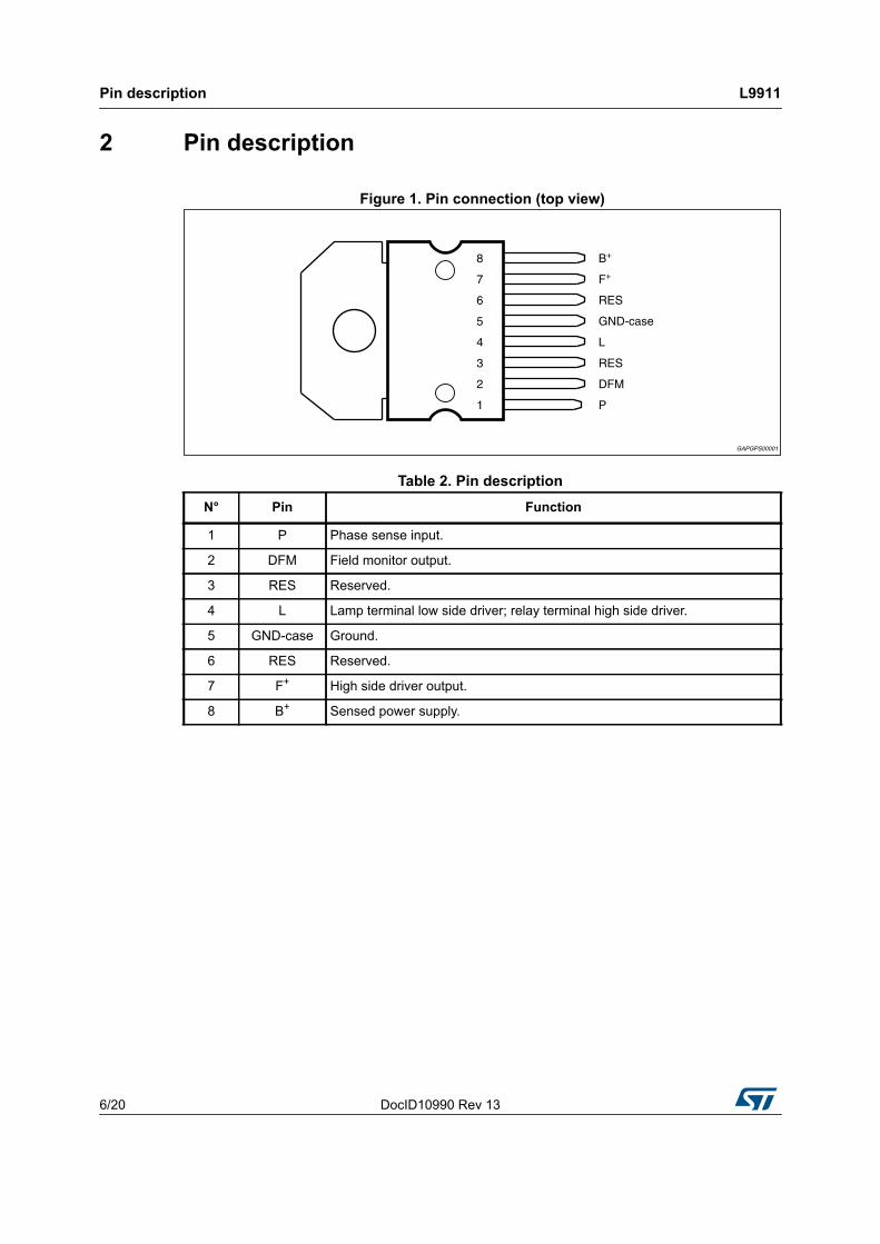
2 Pin description
Figure 1. Pin connection (top view)
Table 2. Pin description N° Pin Function
1 P Phase sense input.
2 DFM Field monitor output.
3 RES Reserved.
4 L Lamp terminal low side driver; relay terminal high side driver.
5 GND-case Ground.
6 RES Reserved.
7 F+ High side driver output.
8 B+ Sensed power supply.

DocID10990 Rev 13 7/20
L9911 Electrical specification
19
3 Electrical specification
3.1 Absolute maximum ratingsTj = -40 to 150 °C, unless otherwise specified.
3.2 Thermal data
3.3 Electrical characteristicsTj = -40 °C to 150 °C; unless otherwise specified.
Table 3. Absolute maximum ratings Symbol Parameter Value Unit
VS DC supply voltage (2 min. @ 25 °C) 24 V
- Transient supply voltage (load dump) [see Figure 8] t < 500 ms 40 V
- Transient supply voltage (low energy spikes) (see Figure 8) ISO7637-1 pulse 1,2,3 /ISO7637-3 60 V
Tj Junction temperature range -40 to 150 °C
Tstg, Tcase Storage and case temperature range -40 to 150 °C
Ptot Total power dissipation (@ Tcase 150°C, Ifield 5A) 4 W
- Reverse battery voltage (see Figure 8) @ 25°C, T = 15 sec. -2.5 V
- Normal working condition reverse voltage (P vs. GND) -1.5 V
- DC pin current on F+, B+, GND (bonding limitation) 15 A
- ESD voltage MILSTD883C (All pins vs.GND) ±4 KV
Table 4. Thermal data Symbol Parameter Value Unit
Rth j-case Thermal resistance junction-to-case ≤1.5 °C/W
Table 5. Electrical characteristics Symbol Parameter Test condition Min. Typ. Max. Unit
Vbat Operating supply voltage - 7 - 18 V
Ib-sinked Supply battery current - - - 25 mA
Ib-stby Standby current B+ = 12.5 V, F+ = 0 V - - 500 μA

Electrical specification L9911
8/20 DocID10990 Rev 13
Vreg 1
Regulated voltage & thermal drift.3 configurations available, selectable by mask option (see Table 8).
Ialt =1 A-0.9 · Inom; Tcase = 20 °C;1400 < rpm < RPMMAX (see Figure 2)
14.0-4.5
14.4-3.5
14.8-2.5
VmV/°C
Vreg 2
Ialt =10 A; Tcase = 23 °C;rpm = 6000 rpm; 15 V max. (see Figure 3)
14.35-11.8
14.5-10
14.65-8.2
VmV/°C
Vreg 3Ialt =10 A; Tcase = 23 °C;rpm = 6000 rpm (see Figure 4)
14.35-6
14.5-4
14.65-2
VmV/°C
Vreg 4Ialt =10 A; Tcase = 23 °C;rpm = 6000 rpm (see Figure 5)
13.95-3.5
14.2-2.5
14.3-1.5
VmV/°C
Vrpm - 1400<rpm<RPMMAX; Ialt = 10 A - - 200 mV
Vload - 5 A<Ialt < Inom; rpm = 6000 rpm - - 250 mV
Vreg-less Reg. voltage without battery Ialt = 3 A resistive; Tcase = 25 °C; 2000 < rpm < RPMMAX 12 - 16 V
Vov-p Overvoltage protection threshold Voltage on pin B+ to disable L drivers
High and low side driver off 18 - 22 V
Vov-d Overvoltage diagnosis threshold VB+ to turn on L low side driver at VF+ > VS1
Vreg -5% Vreg Vreg +
5% V
Tj-sd Thermal shutdown threshold Temperature to disable F+, DFM, L (high & low side drivers) 160 175 190 °C
Tj-sd-dwn Thermal shut-down hysteresisL/F+/DFM from OFF STATE (due to thermal shutdown) to ON STATE
Tj-sd-10 - Tj-sd-
2 °C
Vuv-1Under voltage diagnosis threshold
VB+ to turn on L low side driver 7.7 8.6 9.5 V
Vuv-up VB+ to turn off L low side driver Vuv + 0.40
Vuv + 0.75
Vuv + 1.2 V
VF+_sat Field driver saturation voltageTj = 150 °C; I = 4.5 A - - 0.6 V
Tj = 25 °C; I = 7 A - - 0.55 V
Vf Freewheeling diode F+ I = 5 A - - 2 V
If_SCTH
Field short circuit driver protection threshold current (see Figure 15)
F+ = 0 V; Tj = -40 °C 11 - 18 A
F+ = 0 V; Tj = -25 °C 9.5 - 18 A
F+ = 0 V; Tj = -150 °C 9 - 18 A
Vs1 Field driver ON-state detection - 4.5 - 5.5 V
f-pre Pre-excitation frequency - 283 333 383 Hz
Duty-pre Pre-excitation Field driver ON-duty - 15.93 18.75 21.57 %
tr Output voltage rise time Ifield = 3 A resistivesee Figure 6)
10 - 50 μs
tf Output voltage fall time 10 - 50 μs
Fsw_F+ Field switching frequency Ialt = 1 A~0.9 · Inom; 1400 rpm < rpm < RPMMAX 250 - 400 Hz
Table 5. Electrical characteristics (continued)Symbol Parameter Test condition Min. Typ. Max. Unit

DocID10990 Rev 13 9/20
L9911 Electrical specification
19
If_leak Output field driver leakage current B+ = 24 V; VF+ = 0 - - 10 A
DUTY-PR Phase regulation max field ON duty see Figure 7 26.56 31.25 35.94 %
VH_SATHigh side driver saturation Voltage (see Figure 9) With driver Isource = 500 mA - - 1.5 V
VL_SATLow side driver saturation voltage (see Figure 9) With driver Isink = 500 mA - - 1.5 V
VLSBSelf bias without supply lamp driver voltage
B+ open; L connected to 12 V through a 50 Ohm resistor - - 4 V
IHSCHigh side driver short circuit current protection B+ = 12.5 V; L = GND 1.2 - 3 A
ILSCLow side driver short circuit current (see Figure 15) B+ = L = 12.5 V 1 - 2 A
VthLEnable regulator supply voltage threshold - 0.8 - 1.15 V
Ipd_LL terminal pull-down current when the generator is not rotating VL = 0.6 V 0.4 - 3.5 mA
IL_sinkL sink current when the generator is rotating P frequency 500 Hz; VB+ = 12 V - - 100 μA
t-D Diagnostic alarm delay time - 0.2 - 0.5 s
Vcan-DFMTest mode to cancel soft start/ attack (voltage) (see Figure 10)
30 - 50 V
tcan-DFM Test mode delay time 25 - - ms
VPHL1Enable control voltage input high threshold - - - 0.40 V
VPHL2Enable control voltage input low threshold - - - 0.25(1) V
tPHL1Enable Control Voltage Phase Filtering Time - 50 - 115 μs
VPHH1Diagnosis phase loss input high threshold - 8 9 10 V
VPHH2_1Diagnosis phase loss input low threshold - 6.4 7.4 8.4 V
tPHd Diagnostic phase filtering time - 50 - 100 μs
IPd-P1 Phase pull-down current VP = 0.8 V 1 - 8 mA
f-dfmDFM output open drain switching freq.
Ialt =1 A~0.9 · Inom; 1400 rpm < rpm < RPMMAX; Isink = 4 mA
125 - 200 Hz
VL-DFM Output low voltage saturation I-sink = 14 mA - - 1.5 V
I-SC_DFM Short circuit current protection VB+ = VDFM = 12.5 V 50 - 400 mA
Ilk-DFM Output leakage current VDFM =16 V at DFM driver OFF - - 5 μA
Table 5. Electrical characteristics (continued)Symbol Parameter Test condition Min. Typ. Max. Unit

Electrical specification L9911
10/20 DocID10990 Rev 13
t-TM Output voltage rise timeR = 1 k (see Figure 6)
0.5 - 50μs
t-TD Output voltage fall time 0.5 - 50
1. Guaranteed by design.
Table 5. Electrical characteristics (continued)Symbol Parameter Test condition Min. Typ. Max. Unit
Table 6. Load response control parameters Symbol Parameter Test Condition Min. Typ. Max. Unit
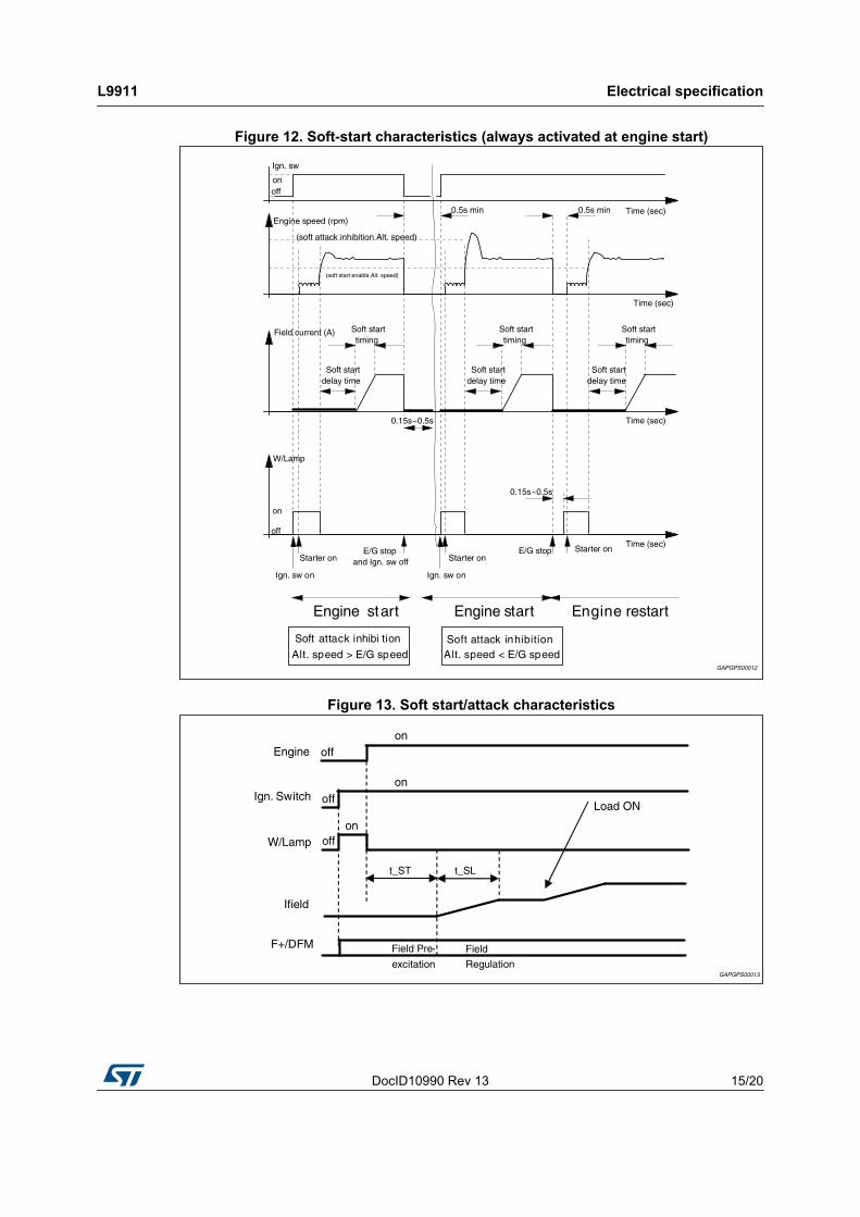
tST_1 Soft start delay time (see Figure 12) 2 steps available, selectable by mask option (see Table 7).
Activated always at engine start
- 0- - s
tST_2 1.73 2 2.35 s
tSL_1 Soft attack time / soft start time (see Figure 12). 2 steps available, selectable by mask option (see Table 7).
From 0 to 100 % field duty cycle
2.13 2.5 2.87
stSL_2 7.65 9 10.35
EN-RES(constant)
Reset frequency range to enable regulation; Frequency judged after 4 periods (see Figure 11)
- 40 50 60 Hz
EN-1
Soft start enable (EN) and LRC disable (DISAB) frequency ranges.4 configurations available, selectable by mask option (possible combinations in Table 8). Always activated at engine start. Frequencies judged after 4 periods (see Figure 11)
Tj = 25 °C Tj = -40 to150 °C
108102
120120
132138
HzHz
EN-2Tj = 25 °C Tj = -40 to150 °C
131124
145145
159166
HzHz
EN-3Tj = 25 °C Tj = -40 to150 °C
144136
160160
176184
HzHz
EN-4Tj = 25 °C Tj = -40 to150 °C
174165
193193
212221
HzHz
DISAB-1Tj = 25 °C Tj = -40 to150 °C
270255
300300
330345
HzHz
DISAB-2Tj = 25 °C Tj = -40 to150 °C
315298
350350
385402
HzHz
DISAB-3Tj = 25 °C Tj = -40 to150 °C
367347
408408
449469
HzHz
DISAB-4Tj = 25 °C Tj = -40 to150 °C
420397
466466
512535
HzHz
Table 7. Load response control timing options - t_SL = 2.5 s t_SL = 9 s
t_ST = 0 s LRC-A LRC-D
t_ST = 0.5 s LRC-C -
t_ST = 2 s LRC-E LRC-B

DocID10990 Rev 13 11/20
L9911 Electrical specification
19
Considering the overall WW application scenario, there is a direct correspondence between Typical configurations A/B and regulation curve Vreg-1, and between typical configuration C and regulation curves Vreg-2 and Vreg-3. This is allowing the summary of all possible customization for L9911 in the table below.
Figure 2. Vreg-1
Table 8. Correspondence of frequency (typical values) to application features Alternator revolution speed (rpm) 6 pole pairs 8 pole pairs
Typical configuration A (Config-A)
Initiate regulation 1200 EN-1 EN-3
LRC Cut 3000 DISAB-1 DISAB-3
Typical configuration B (Config-B)
Initiate Regulation 1450 EN-2 EN-4
LRC Cut 3000 DISAB-1 DISAB-3
Typical configuration C (Config-C)
Initiate Regulation 1450 EN-2 EN-4
LRC Cut 3500 DISAB-2 EN-4
Table 9. Customization of L9911: combination of LRC, regulation, and application options
LRC timing
options
Vreg-1/Config-A Vreg-1/Config-B Vreg-2/Config-B Vreg-2/Config-A Vreg-4/Config-A
6 Pole Pairs
8 Pole Pairs
6 Pole Pairs
8 Pole Pairs
6 Pole Pairs
8 Pole Pairs
6 Pole Pairs
8 Pole Pairs
6 Pole Pairs
8 Pole Pairs
LRC-A L9911P nya nya nya nya nya nya nya L9911K nya
LRC-B nya nya L9911F nya L9911I nya nya nya nya nya
LRC-C nya nya nya nya nya nya L9911V nya nya nya
LRC-D nya nya nya nya nya nya nya nya nya nya
LRC-E L9911U nya nya nya nya nya nya nya nya nya

Electrical specification L9911
12/20 DocID10990 Rev 13
Figure 3. Vreg-2
Figure 4. Vreg-3

DocID10990 Rev 13 13/20
L9911 Electrical specification
19
Figure 5. Vreg-4
Figure 6. Output voltage rise/fall time (F+, DFM)
Figure 7. Phase regulation characteristics

Electrical specification L9911
14/20 DocID10990 Rev 13
3.4 Principle of phase regulationWhen VB+ is above the regulated voltage, the field driver is controlled to keep phase peak voltage from falling below VPHH1.
If phase peak voltage drops below VPHL1, phase regulation does not work.
Figure 8. Application diagram
Figure 9. High side/low side driver saturation
Figure 10. Test mode to cancel soft-start/attack
Figure 11. Soft-start enable frequency range
DocID10990 Rev 13 15/20
L9911 Electrical specification
19
Figure 12. Soft-start characteristics (always activated at engine start)
Figure 13. Soft start/attack characteristics
Electrical specification L9911
16/20 DocID10990 Rev 13
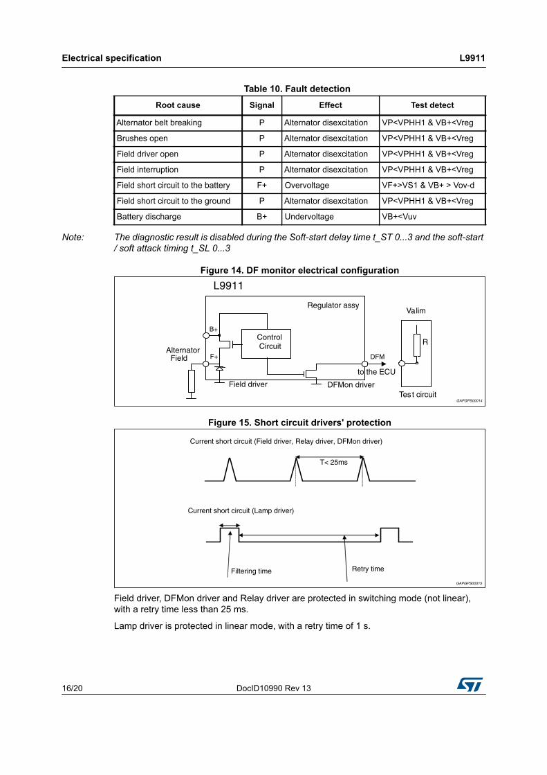
Note: The diagnostic result is disabled during the Soft-start delay time t_ST 0...3 and the soft-start / soft attack timing t_SL 0...3
Figure 14. DF monitor electrical configuration
Figure 15. Short circuit drivers' protection
Field driver, DFMon driver and Relay driver are protected in switching mode (not linear), with a retry time less than 25 ms.
Lamp driver is protected in linear mode, with a retry time of 1 s.
Table 10. Fault detection Root cause Signal Effect Test detect
Alternator belt breaking P Alternator disexcitation VP<VPHH1 & VB+<Vreg
Brushes open P Alternator disexcitation VP<VPHH1 & VB+<Vreg
Field driver open P Alternator disexcitation VP<VPHH1 & VB+<Vreg
Field interruption P Alternator disexcitation VP<VPHH1 & VB+<Vreg
Field short circuit to the battery F+ Overvoltage VF+>VS1 & VB+ > Vov-d
Field short circuit to the ground P Alternator disexcitation VP<VPHH1 & VB+<Vreg
Battery discharge B+ Undervoltage VB+<Vuv
DocID10990 Rev 13 17/20
L9911 Package information
19
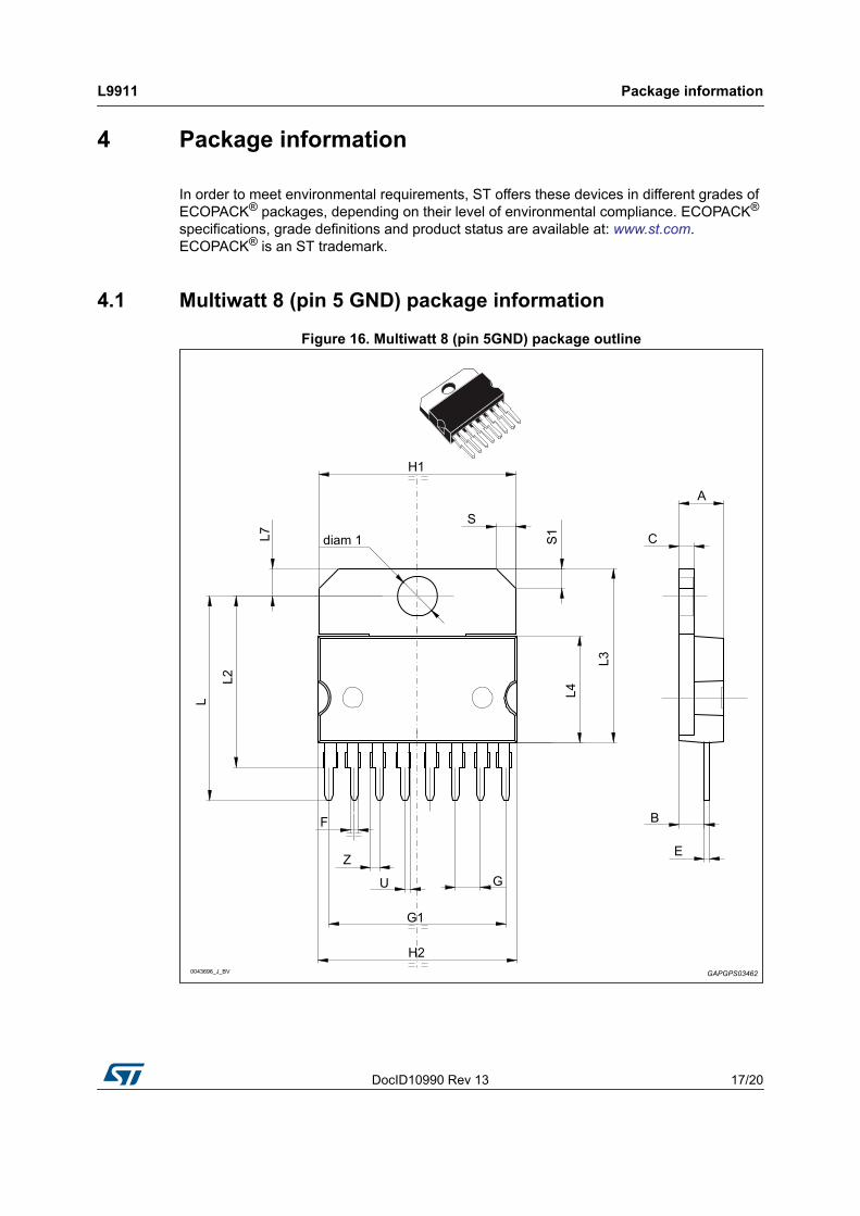
4 Package information
In order to meet environmental requirements, ST offers these devices in different grades of ECOPACK® packages, depending on their level of environmental compliance. ECOPACK® specifications, grade definitions and product status are available at: www.st.com. ECOPACK® is an ST trademark.
4.1 Multiwatt 8 (pin 5 GND) package information
Figure 16. Multiwatt 8 (pin 5GND) package outline

Package information L9911
18/20 DocID10990 Rev 13
Table 11. Multiwatt 8 (pin 5GND) package mechanical drawing
Ref
Dimensions
Millimeters Inches(1)
1. Values in inches are converted from mm and rounded to 4 decimal digits.
Min. Typ. Max. Min. Typ. Max.
A - - 5 - - 0.1969
B - - 2.65 - - 0.1043
C - - 1.6 - - 0.0630
E 0.49 - 0.55 0.0193 - 0.0217
F 0.78 - 0.85 0.0307 - 0.0335
G 2.40 2.54 2.68 0.0945 0.1000 0.1055
G1 17.64 17.78 17.92 0.6945 0.7000 0.7055
H1 19.6 - - 0.7717 - -
H2 - - 20.2 - - 0.7953
L 20.35 20.65 0.8012 0.8130
L2 17.05 17.20 17.35 0.6713 0.6772 0.6831
L3 17.25 17.5 17.75 0.6791 0.6890 0.6988
L4 10.3 10.7 10.9 0.4055 0.4213 0.4291
L7 2.65 - 2.9 0.1043 - 0.1142
S 1.9 - 2.6 0.0748 - 0.1024
S1 1.9 - 2.6 0.0748 - 0.1024
U 0.40 - 0.55 0.0157 - 0.0217
Z 0.70 - 0.85 0.0276 - 0.0335
diam1 3.65 - 3.85 0.1437 - 0.1516

DocID10990 Rev 13 19/20
L9911 Revision history
19
5 Revision history
Table 12. Document revision history Date Revision Changes
22-Jun-2004 1 Initial release.
18-May-2005 2Modified Figure 2, Table 2 and Table 5; Updated Figure 10, 11 and 14; Add Table 7. Add ordering numbers.
07-Nov-2005 3Updated Table 5.Added new tables 6-9.
28-Nov-2005 4Added the L9911C part number.Updated the Table 9.
11-Jul-2007 5Document reformatted.Updated order codes, see Table 1: Device summary.
09-Nov-2009 6Updated Table 1: Device summary, Table 7: Load response control timing options and Table 9: Customization of L9911: combination of LRC, regulation, and application options.
23-Jul-2010 7
Updated Table 1: Device summary, Table 5: Electrical characteristics and Table 9: Customization of L9911: combination of LRC, regulation, and application options.Updated Figure 2, 3 and 4.Added new Figure 5.
25-Jan-2011 8Updated Table 5: Electrical characteristics.Updated Figure 5.
29-Mar-2011 9 Modified in the Table 5: Electrical characteristics the values of the “Vuv-up” parameter.
26-Mar-2012 10
Updated:Table 1: Device summary on page 1;Table 7: Load response control timing options on page 10;Table 9: Customization of L9911: combination of LRC, regulation, and application options on page 11.
28-May-2012 11 Updaded Table 9: Customization of L9911: combination of LRC, regulation, and application options on page 11.
19-Sep-2013 12 Updated disclaimer.
30-Sep-2015 13 Added Section 1.5: Self start function on page 5.

L9911
20/20 DocID10990 Rev 13
IMPORTANT NOTICE – PLEASE READ CAREFULLY
STMicroelectronics NV and its subsidiaries (“ST”) reserve the right to make changes, corrections, enhancements, modifications, and improvements to ST products and/or to this document at any time without notice. Purchasers should obtain the latest relevant information on ST products before placing orders. ST products are sold pursuant to ST’s terms and conditions of sale in place at the time of order acknowledgement.
Purchasers are solely responsible for the choice, selection, and use of ST products and ST assumes no liability for application assistance or the design of Purchasers’ products.
No license, express or implied, to any intellectual property right is granted by ST herein.
Resale of ST products with provisions different from the information set forth herein shall void any warranty granted by ST for such product.
ST and the ST logo are trademarks of ST. All other product or service names are the property of their respective owners.
Information in this document supersedes and replaces information previously supplied in any prior versions of this document.
© 2015 STMicroelectronics – All rights reserved