cadence circuit design tools - turku centre for … introduction and objectives we have two...
TRANSCRIPT

Mikko Pankaala | Sami Nuuttila
Cadence Circuit Design Tools
TUCS Technical ReportNo 831, June 2007


Cadence Circuit Design Tools
Mikko PankaalaUniversity of Turku, Department of Information TechnologyJoukahaisenkatu 3-5, 20520 Turku, [email protected]
Sami NuuttilaUniversity of Turku, Department of Information TechnologyJoukahaisenkatu 3-5, 20520 Turku, [email protected]
TUCS Technical Report
No 831, June 2007

Abstract
This document is an attempt to give a short description of available Cadence toolsfor circuit design through Europractise (2006/2007 Release) at the University ofTurku. It tries to answer two questions: What kind of tools wehave? and Whatare they for? Moreover, a selected set of the most important system files anddirectories related to analog IC design are examined more closely.
Keywords: CADENCE, IC design
TUCS LaboratoryMicroelectronics

1 Introduction and Objectives
We have two objectives for writing this document. First, to increase the knowl-edge of available Cadence circuit design tools among users at our department.Second, we provide information what are the tools for.
However, the purpose is not to provide an exhaustive study ofall available tools,but merely to give a short description of the main features ofeach tool and therebyto encourage users to find out more of the tools that could be useful for their pur-poses. The focus is on analog circuit design tools, but some tools for digital designare also introduced to get a more comprehensive insight of Cadence’s tool reper-toire.
One of the reasons that gave rise to writing this document wasthat by providingthe basic knowledge about the most important Cadence related system files (foranalog IC design) could help people to fix the most common problems by them-selves.
2 Cadence Circuit Design Tools
This chapter introduces different Cadence circuit design tools available at the Uni-versity of Turku. Tools are provided by Europractice and the2006/2007 releaseis of specific interest. A more or less complete list of this release can be found athttp://www.msc.rl.ac.uk/europractice/software/cadence 06 07.html. If you lookat the webpage, most of the software listed underIC Packageare installed andthe rest can (probably) be installed by request. The contents of the IC Package isreplicated in tables 1 and 2 on the next pages. Table 1 lists the tools for digital andmixed-mode design and table 2 for analog and mixed-mode design respectively. Itcan be expected that even more than before, more specializedtools are introducedas processing technology develops towards smaller and smaller devices. But thatis another story. Next we will take a look where we are now. After the list, themain features of each tool are discussed.
Notice that most of the tools are embedded tightly to the Cadence Design Frame-work and do not have specific graphical user interface (GUI) of their own. Theonly cue of their existence can be an additional menu in some other tool. To getan idea of the tools available at your current set up start CIW(eg. with commandicfb), chooseCIW − > Options − > License. . . and check the list of availablelicenses.
1
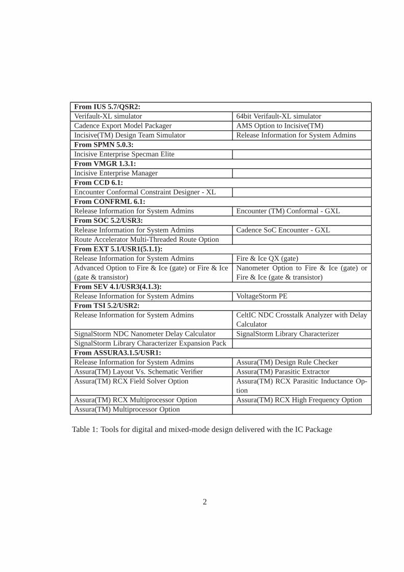
From IUS 5.7/QSR2:Verifault-XL simulator 64bit Verifault-XL simulatorCadence Export Model Packager AMS Option to Incisive(TM)Incisive(TM) Design Team Simulator Release Information for System AdminsFrom SPMN 5.0.3:Incisive Enterprise Specman EliteFrom VMGR 1.3.1:Incisive Enterprise ManagerFrom CCD 6.1:Encounter Conformal Constraint Designer - XLFrom CONFRML 6.1:Release Information for System Admins Encounter (TM) Conformal - GXLFrom SOC 5.2/USR3:Release Information for System Admins Cadence SoC Encounter - GXLRoute Accelerator Multi-Threaded Route OptionFrom EXT 5.1/USR1(5.1.1):Release Information for System Admins Fire & Ice QX (gate)Advanced Option to Fire & Ice (gate) or Fire & Ice(gate & transistor)
Nanometer Option to Fire & Ice (gate) orFire & Ice (gate & transistor)
From SEV 4.1/USR3(4.1.3):Release Information for System Admins VoltageStorm PEFrom TSI 5.2/USR2:Release Information for System Admins CeltIC NDC Crosstalk Analyzer with Delay
CalculatorSignalStorm NDC Nanometer Delay Calculator SignalStorm Library CharacterizerSignalStorm Library Characterizer Expansion PackFrom ASSURA3.1.5/USR1:Release Information for System Admins Assura(TM) Design Rule CheckerAssura(TM) Layout Vs. Schematic Verifier Assura(TM) Parasitic ExtractorAssura(TM) RCX Field Solver Option Assura(TM) RCX Parasitic Inductance Op-
tionAssura(TM) RCX Multiprocessor Option Assura(TM) RCX High Frequency OptionAssura(TM) Multiprocessor Option
Table 1: Tools for digital and mixed-mode design delivered with the IC Package
2

From IC 5.1.41/ISR:Cadence Design Framework II Cadence Design Framework Integrator’s
Toolkit64bit Cadence Design Framework Int Virtuoso PreviewVirtuoso Simulation Environment Virtuoso Schematic VHDL InterfaceVirtuoso Schematic Editor Verilog Interface Virtuoso Schematic Editor HSPICE Inter-
faceVirtuoso-XL Layout Editor 64bit Virtuoso Layout EditorVirtuoso Compactor Virtuoso Layout Editor TurboVirtuoso Analog Oasis Run-Time Option Cadence OASIS for RFDEVirtuoso Electronic Design for ManufacturabilityOption
Spectre Third-party Simulator Interface
Spectre Verilog-A Simulation Option Spectre/-RF - Cadence SPW Model LinkOption to Spectre RF
Spectre-RF IC Package Modeler Option Virtuoso Analog HSPICE Interface OptionVirtuoso Schematic Editor Virtuoso Analog Design EnvironmentSpectre-RF Substrate Coupling Analysis Option Virtuoso Analog VoltageStorm OptionVirtuoso Analog ElectronStorm Option Virtuoso Layout MigrateStructure Compiler Virtuoso Schematic Composer to design
compiler integrationCadence(R) RC Network Reducer Option Virtuoso AMS Designer EnvironmentDracula Design Rule Checker 64bit Dracula Design Rule CheckerDracula Layout Vs. Schematic Verifier 64bit Dracula Layout Vs. SchematicDracula Parasitic Extractor 64bit Dracula Parasitic ExtractorDiva Design Rule Checker 64bit Diva Design Rule CheckerDiva Layout Vs. Schematic Verifier 64bit Diva Layout Vs. Schematic VerifierDiva Parasitic Extractor Release Information for System AdminsCadence SKILL Development Environment Virtuoso EDIF 300 Connectivity
Reader/WriterVirtuoso EDIF 300 Schematic Reader/Writer Cadence team design project administratorFrom ICC 11.2.41/USR3:Virtuoso Chip Assembly RouterFrom MMSIM 6.0/ISR:Virtuoso Spectre Circuit Simulator Virtuoso Spectre Model Interface OptionVirtuoso Spectre-RF Simulation Option Spectre/-RF - Cadence SPW Model Link
Option to Spectre RFVirtuoso UltraSim Full-chip Simulator Virtuoso RelXpertRelease Information for System AdminsFrom AES 1.0:Cadence Advanced Encryption Standard-64bitFrom NEOCKT 3.3/ISR(3.3.4):Virtuoso NeoCircuit DFM Release Information for System AdminsELDO Interface to Virtuoso NeoCircuit HSPICE Interface to Virtuoso NeoCircuitADS Interface to Virtuoso NeoCircuitFrom VSDE 4.1/USR1:Virtuoso Parallel Analysis Option Virtuoso Specification-driven EnvironmentVirtuoso Characterization & Modeling option forthe Specification-driven Environment
Virtuoso Optimization option for theSpecification-driven Environment
Table 2: Tools for analog and mixed-mode design delivered with the IC Package
3
2.1 Tools for Digital and Mixed-mode design
The tools listed in the following are divided into two gategories. The first set oftools is for front-end digital design (logic design and verification) and the secondis for back-end design (place & route, delay calculation, timing analysis etc.). Thelist is not comprehensive, but tries to cover the most relevant tools.
2.1.1 Logic Design and Verification
NCLaunchNCLaunch provides you with a graphical user interface to configure and launchyour Cadence simulation tools.
NC-VHDL simulatorThe Cadence NC-VHDL simulator C Interface (CIF) is part of the Open Archi-tecture of the Cadence NC-VHDL simulator product. The Open Architecture is acollection of libraries that allow access to the NC-VHDL simulator environment.The Open Architecture includes:
• The C Function Call library (CFC)The CFC library lets you call C functions from the simulator command line.
• The Foreign Model Import library (FMI)The FMI library enables models written in the C programming languageand VHDL subprograms to be executed by the simulator.
• The VHDL Design Access library (VDA)The VDA library contains a set of routines and definitions formanipulatingVHDL objects, scopes, values, and types.
SimVisionSimVision is a unified graphical debugging environment for Cadence simulators.You can use SimVision to debug digital, analog, or mixed-signal designs writtenin Verilog, VHDL, SystemC, or a combination of those languages.
NC-Verilog simulatorThe Cadence NC-Verilog simulator is a Verilog digital logicsimulator that com-bines the high-performance of native compiled code simulation with the accuracy,flexibility, and debugging capabilities of event-driven simulation. The NC-Verilogsimulator is based on Cadence’s Interleaved Native Compiled Code Architecture(INCA).
NC-SystemC simulatorSystemC, as an industry standard for system-level design modeling, supports thedescription of the architecture of complex systems consisting of both software and
4

hardware components. The SystemC environment is the C++ programming lan-guage with additional semantics introduced by the SystemC Class Library. Thislibrary provides the constructs necessary to model system architecture, includinghardware timing, concurrency, and reactive behavior.
The Cadence SystemC Design and Verification environment, aspart of the Inci-siveTM unified simulation platform, consists of a set of simulation and debuggingcapabilities that allows you to address your needs in both the design and verifica-tion of system hardware and software. The NC-SystemC simulator is a platformfor simulation and debugging SystemC models, either pure ormixed with Verilogor VHDL.
Verifault-XLVerifault-XL is a fault simulation system that operates within the Verilog-XL envi-ronment using the same libraries that Verilog-XL uses. Verifault-XL allows chip,board, and system designers to simulate the faults that can occur in the hardwarerepresented by their design descriptions and to develop test vectors that can detectthose faults.
Verifault-XL simulates faults at the gate-and-switch, or structural, level. However,your circuit descriptions may contain elements that are described using behav-ioral constructs. Therefore, Verifault-XL lets you propagate the effects of faultsthrough both structural and behavioral constructs, makingit a true mixed-levelfault simulator.
Verifault-XL supports bit annotation, which lets you placebuses in specific blocksfor timing constructs. As a result, you do not need to split the individual bits of abus to apply timing information to them.
Cadence HDL analysis and lint (HAL)HAL is a design rule checker for Verilog Hardware Description Language (HDL),Very High-speed integrated circuit Hardware Description Language (VHDL), Sys-temC and Mixed Language designs.
HAL helps you find coding errors early in your design process,before you simu-late your design. The tool identifies coding errors and improper register transferlevel (RTL) design styles through a comprehensive analysisof your HDL sourcecode.
IP Model PackagerThe IP Model Packager is a model export tool that creates a protected model. Youcan simulate a packaged model in standard HDL simulation environments withthe model manager software that is included in the packaged model.
5

Note: To use the IP Model Packager most effectively, you should befamiliarwith performing digital design and analysis using either the Verilog HardwareDescription Language (HDL), or the Very High Speed Integrated Circuit Hard-ware Description Language (VHDL), and you should be familiar with either theVerilog-XL simulator or the Cadence NC simulator.
Incisive CoverageCoverage analysis at the RTL or behavioral level is analogous to fault coverageat the gate level. Performing coverage analysis prior to synthesis reduces the testverification cycle by moving the process to a higher level of abstraction where thetestbench is more easily understood with regard to the code it is testing.
Without code coverage, the design engineer can only guarantee that the outputsfrom functional simulation match the expected results for agiven set of test vec-tors; there is no way to ensure the effectiveness of the test vectors. Without know-ing how well the test vectors are exercising the design, the designer does not knowif more test vectors are needed, where more test vectors are needed, or when tostop simulating. Incisive Coverage Technology enables thedesigner to answer allof these questions.
Using Coverage Technology prior to synthesis is the most productive way of us-ing the tool. The coverage tool supports coverage analysis at all levels of designabstraction and for all Verilog/VHDL language constructs.The coverage tool en-ables designers and design verification engineers to generate a quantitative answerto the question: Have we simulated our design enough to commit it to synthesis?
Incisive Coverage Technology works in conjunction with HDLsimulation to quan-tify how well the test vectors exercise the design and to identify parts of a designthat require more testing. Coverage analysis reports identify
• Design areas not completely tested,
• Redundancy in testing, and
• Unused portions of the design that can be removed before synthesis.
The Finite State Machine (FSM) monitoring capability givesyou a unique wayof quantifying coverage of the control portions of the design. USX technologyperforms a synthesis interpretation of the control logic and provides analysis us-ing FSM representation. Together with code coverage analysis, The coverage toolprovides a comprehensive, quantitative measure of the quality of the simulationtests applied to a design.
6

FormalCheck Model CheckerThe Cadence FormalCheck Model Checker verifies synthesizable Verilog Hard-ware Description Language (Verilog HDL) and Very High-Speed Integrated Cir-cuit Hardware Description Language (VHDL) designs. FormalCheck is designedto operate as a companion to any digital simulator for Verilog or VHDL.
FormalCheck functionally verifies a VHDL or Verilog design against a designspecification by answering the question: ”Does my design function according toits specification?” FormalCheck does this through model checking, rather than us-ing test vectors or testbenches.
Model checking is an algorithmic procedure to verify that a design possesses des-ignated properties. The procedure analyzes all possible behaviors of a design, andcan verify properties with mathematical certainty. Applying model checking toa design corresponds to simulating the design for every possible test vector se-quence for an infinite number of arbitrarily long tests.
Using model checking techniques, FormalCheck finds design errors that are diffi-cult or impossible to detect using traditional simulation tools. These errors includethose that occur under complex, hard-to-anticipate sequential conditions. Whilesuch errors are notoriously difficult to find, either with designed or random testvectors, they are routinely detected by a model checker.
The FormalCheck Model Checker detects errors in a fully automated fashion. Thismeans that a FormalCheck automated verification run does notrequire you to an-ticipate errors. Thrashing (livelock) conditions, which cannot be detected directlyby simulators at all, are also found with fully automated model checking.
Model checking is most effective on ”control-intensive” designs (designs withoutextensive data paths). You may verify properties that you define in FormalCheckwith a digital simulator on those portions of a design where model checking isless effective. This is supported by a utility that transforms the properties into atestbench for the simulator.
It is not necessary to have any specialized mathematical knowledge, nor is it nec-essary to learn a specific model checking language to use FormalCheck. For-malCheck can be used with familiar HDL language constructs and command-lineinterface (CLI) commands to verify designs.
7
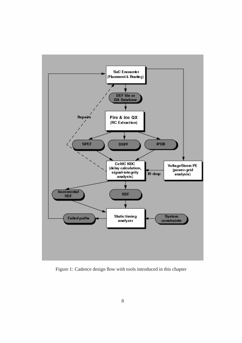
Figure 1: Cadence design flow with tools introduced in this chapter
8

2.1.2 Encounter Family for Back-end Design
Figure 1 presents Cadence design flow with the tools introduced in the following.
SoC Encounter - GXLThe Encounter family consists of four products:
• First Encounter Ultra silicon virtual prototyping solution
• Nano EncounterTM implementation system for flat designs
• Nano Encounter Demand-Based Savings (DBS) system
• SoC EncounterTM hierarchical RTL-to-GDSII physical implementation so-lution
• (NanoRouteTM Ultra SoC routing solution)
The First Encounter Ultraproduct includes the following features:
• RTL synthesisCreates a gate-level netlist from Register Transfer Language (RTL) input.
• Virtual prototyping and placementProvides quick feedback on the design performance. With this feature, youfirst create a block-and-cell placement, then perform trialrouting, analyzetiming, and refine the design to meet your specifications.
• Hierarchical partitioning and block placementLets you create a hierarchical design consisting of a top-level floorplanthat contains blocks you implement separately. At the top level you defineblocks, analyze congestion and timing, and refine the designas needed. Thesystem automatically creates timing budgets and optimizedpin locations touse in physical implementation.
• Timing optimizationProvides in-place optimization, which improves timing by inserting buffersand resizing gates, without changing the design’s logic. Includes a physicalsynthesis solution to close timing for difficult blocks.
The Nano Encounterproduct includes the following features for flat design flows:
• Support for 90 nm and 130 nm process rules
• Virtual prototyping and placement
• Physical synthesis optimizationNote: You cannot perform RTL synthesis.
9

• WRoute routerProvides traditional grid-based global and detailed routing of signal andclock nets.
• Power routerProvides the ability to create power rings and stripes, and perform powerrouting.
• NanoRoute routerProvides high-speed graph-based global and detailed routing for large-capacitydesigns.
• Geometry, connectivity, and antenna verification
• Signal wire editing
• Block antenna abstract creation
• GDSII generation
An optional Route Accelerator license provides multi-thread capability that letsyou run WRoute and NanoRoute on multiple CPUs.
Nano Encounter Demand-Based Savings (DBS)The Nano Encounter DBS product is a cost-saving alternativeto Nano Encounterthat provides all of the major features of Nano Encounter, but for smaller designs.Each Nano Encounter DBS license supports designs with up to 300,000 place-able instances (excluding filler cells). If your design grows beyond that limit,Encounter can check out additional Nano Encounter DBS licenses to support thelarger design.
The Nano Encounter DBS user interface provides access to allof the major NanoEncounter components, including NanoRoute, WRoute, SRoute, and ClockWise.However, with the exception of WRoute, the interface does not support use ofthese tools in standalone mode, and it does not support the Coyote field solver.Additionally, support for multi-threading with Nano Encounter DBS requires aseparate Route Accelerator license for each additional thread.
NanoRoute UltraThe NanoRoute Ultra product is a self-contained, block-level and top-level rout-ing solution for system-on-chip (SoC) designs. It has the same features as NanoEncounter, except for virtual prototyping and placement.
The SoC Encounterproduct is a full hierarchical floorplanning and routing solu-tion. It provides a broad spectrum of features, including the following featurescontained in First Encounter Ultra and Nano Encounter:
10

• RTL synthesis
• Virtual prototyping and placement
• Hierarchical partitioning and block placement
• Timing optimization
• Virtual prototyping and placement
• Physical synthesis optimization
• WRoute router
• Power router
• NanoRoute router
• Geometry, connectivity, and antenna verification
• Signal wire editing
• Block antenna abstract creation
• GDSII generation
SoC Encounter also includes the following feature, which isnot included in theother Encounter products:
• Sign-off signal integrityThe CeltICTM crosstalk analyzer for cell-based design prevents, calculates,and repairs crosstalk noise caused by interconnect coupling. This tool canalso calculate and repair glitch noise and the delay effectsof noise for statictiming analysis.
SoC Encounter provides an easy upgrade path from the SiliconEnsemble family,with legacy support.
Voltage Storm PEVoltageStorm PE is designed to help you verify that the power-grid network onyour chip does not suffer from IR drop, ground bounce, or electromigration prob-lems.
Because VoltageStorm PE does not require the signal routingof your design tobe complete before power-grid analysis, it enables you to verify and change yourpower grid early in the design cycle.
VoltageStorm PE offers the following features:
11

• Multi-level hierarchical power-grid verification
• Pass/fail power-grid validation
• Accurate embedded 130 nanometer and below parasitic extraction that mod-els effects resulting from advanced copper processes, suchas chemical me-chanical polishing (CMP), such as erosion, dishing, and slotting, and opticaleffects, such as non-trapezoidal wires and wire-edge enlargement.
• Integration with Cadence SoC Encounter
• Integration with CeltIC NDC
• Support for multiple design formats such as LEF/DEF, GDSII,a mixture ofDEF and GDSII, or OpenAccess 2.2
• Static and dynamic gate-level power-grid analysis
• Instance-based static and dynamic power-consumption analysis, includingIP and memories
• Hierarchical power-grid analysis and signoff for cell-based designs
• Power distribution estimation for hard IPs and macros
• Power planning
• User-selectable power-ground short detection
• Via clustering
• “What if” analysis using PGS Exploration, which enables youto interac-tively experiment to fix problems and optimize the power distribution net-work
• Use of power-grid views to efficiently support designs that contain customor IP blocks
• Selective accuracy to support early verification and signoff accuracy
• Standard interfaces
• Package modeling
CeltIC NDC Crosstalk Analyzer with Delay CalculatorThe CeltICTM crosstalk analyzer analyzes and fixes crosstalk-related functionaland timing problems for cell-based designs. It calculates noise-induced delaychanges for static timing analysis and generates repairs for place-and-route.
CeltIC offers the following features:
12

• Characterize the cell library for noise.
• Calculate crosstalk noise caused by interconnect coupling.
• Filter out false noise failures.
• Calculate crosstalk-induce delay and slew changes for Static Timing Anal-ysis (STA).
• Generate ECO repairs for optimization.
Physically Knowledgeable Synthesis (PKS)Cadence Physically Knowledgeable Synthesis (PKS) is a Cadence physical syn-thesis product and a part of the unified synthesis and place-and-route (SP&R)flow. PKS provides physical placement and timing information in combinationwith logic synthesis (BuildGates Synthesis) to resolve thetiming closure issuesthat currently plague conventional synthesis. Its purposeis to provide logic syn-thesis technology with a means to accurately predict timingbased on the incre-mental physical placement of cells during the optimizationprocess.
Fire & Ice QX (gate)Fire & Ice QX (QX) is an accurate, high-capacity, high-performance gate-levelparasitic resistance and capacitance extractor that is fast enough to use after everydetailed routing session.
In 0.13µm and below processes, signal delay due to interconnect parasitics be-comes much more significant than the contribution to signal delay due to the in-herent cell delays. Approximately 80% of the delay for most paths is now dueto interconnect delays. Therefore accurate modeling of theparasitics on the inter-connects is vital for high performance chip designs. Also, signal integrity analysisrequires accurate coupling capacitance extraction. However, accuracy of parasiticextraction comes at a cost - in terms of run time for performing the extraction. Itis a function of design size, process, desired results, and the number and configu-rations of systems that are available to do the extraction.
Three-Dimensional Interconnect Modeling and RCgen
Cadence tools use analytical modeling to model the interconnect parasitic capac-itance and resistance of an integrated circuit design. QX uses a technology file,created from the fabrication process information, along with cell library data andthe design itself, for resistance and capacitance extraction. The fabrication pro-cess information is entered into an ASCII-format interconnect technology (ICT)input file from which RCgen generates a technology file for QX.This technologyfile is often created and validated by the major foundries. This file contains inter-connect models used by QX to extract the interconnect parasitic capacitance and
13
resistance. For resistance extraction, it contains resistance information on each in-terconnect layer and via; for capacitance extraction, it contains three-dimensionalinterconnect models.
2.2 Tools for Analog and Mixed-mode design
Cadence IC package includes a wide variety of different tools for analog andmixed-mode design, as can be seen in table 2. The most important tools are dis-cussed next.
2.2.1 AMS Environment
The AMS flow uses the AMS environment and a set of tools tuned tofacilitate thedevelopment of mixed-signal designs. The flow gives you a mixed-signal, mixed-language, block-based design solution featuring the following characteristics.
• A top-down or bottom-up development methodology for both analog andmixed-signal designs.
• The ability to mix blocks at different levels of abstractionfor an optimizedbalance of simulation accuracy versus speed
• The ability to create Verilog-AMS netlists for an entire library with a singlecommand
• Automatic, non-destructive conversion of existing analogprimitive libraries
• A design capture environment that facilitates both text andschematic dataentry
• Support for the Verilog-AMS, VHDL-AMS, Spectre, and SPICE languages
• Flexible and accurate representation of analog/digital interface boundariesand accurate, automatic insertion of interface elements
• Flexible and accurate representation of mixed-language boundaries
• Flexible design configuration, which allows easy switchingfrom one designrepresentation to another
• Accelerated, automatic netlist generation from schematics
• A single debugging environment for analog, digital, and mixed-signal partsof your design
14

• Stand-alone simulation when desired
• A single unified waveform display for analog, digital, and mixed signal netsin your design
The tools in the AMS flow work smoothly together, so you can move from onetool to another without worrying about whether your data is in the necessary for-mat. For example, when you work within the flow, you can develop a schematic,define a configuration, and then simulate without working through a netlistingstep: the flow netlists the design for you as needed or uses a netlist created bysomeone else for a block you are referencing.
2.2.2 Cadence analog design environment(ADE)
The features of the Cadence analog design environment
• Consistent User Interface
• Analog Design Entry
• Design Hierarchy
• Annotation
• Interactive Simulation
• Simulation Output and Analysis
• Parametric Analysis
2.2.3 Waveform Calculator
The Waveform Calculator is a scientific calculator with bothalgebraic and ReversePolish Notation (RPN) modes. You can use it to
• Build, print, and plot expressions containing your simulation output data
• Enter expressions, which can contain node voltages, port currents, operatingpoints, model parameters, noise parameters, design variables, mathematicalfunctions, or arithmetic operators, into a buffer
• Store the buffer contents into a memory and then recall the memory contentsback into the buffer
• Save calculator memories to a file and load those memories back into thecalculator
15

2.2.4 Cadence mixed-signal circuit design environment (icms)
The features of the Cadence mixed-signal circuit design environment let you cre-ate, simulate, and analyze designs containing both analog and digital components.
Mixed-signal design examples are available for you to try out the mixed-signalflow on CDBA. They are located in/soft/cadence/ic5033usr2/tools/dfII/samples/artist/mixSig. See README file.
2.2.5 SKILL language
The Cadence SKILL language is a high-level, interactive programming languagebased on the popular artificial intelligence language, Lisp. However, the SKILLlanguage supports a more conventional C-like syntax. This support allows anovice user to quickly learn to use the system, while expert programmers canaccess the full power of the Lisp language. At the simplest level, SKILL is aseasy to use as a calculator. At the most sophisticated level,SKILL is a powerfulprogramming language whose applications are virtually unlimited.
SKILL brings to the command line a functional interface to the underlying sub-systems. SKILL lets you quickly and easily customize existing CAD applicationsand helps you develop new applications. SKILL has functionsto access each Ca-dence tool using an application programming interface.
2.2.6 Open Command Environment for Analysis (OCEAN)
OCEAN lets you set up, simulate, and analyze circuit data. OCEAN is a text-based process that you can run from a UNIX shell or from the Command Inter-preter Window (CIW). You can type OCEAN commands in an interactive session,or you can create scripts containing your commands, then load those scripts intoOCEAN. OCEAN can be used with any simulator integrated into the CadenceAnalog Design Environment.
Typically, you use the Cadence analog design environment when creating yourcircuit (in Composer) and when interactively debugging thecircuit. After thecircuit has the performance you want, you can use OCEAN to runyour scriptsand test the circuit under a variety of conditions. After making changes to yourcircuit, you can easily rerun your scripts. OCEAN lets you
• Create scripts that you can run repeatedly to verify circuitperformance
• Run longer analyses such as parametric analyses, Corners Analyses, andstatistical analyses more effectively
16

• Run long simulations in OCEAN without starting the Cadence analog de-sign environment graphical user interface
• Run simulations from a nongraphic, remote terminal
OCEAN examples are located in/soft/cadence/ic5033usr2/tools/dfII/samples/artist/OCEAN. See README file.
2.2.7 Virtuoso Specification-driven Environment (SdE)
The Virtuoso Specification-driven Environment (SdE) is an interactive design en-vironment for the analysis, characterization, and verification of analog, digital,and mixed-signal circuits. The SdE is also integrated with the Virtuoso SchematicEditor and can be used with multiple designs simultaneously.
Note: The Virtuoso Specification-driven Environment is OpenAccess compliant.
The Virtuoso Specification-driven Environment helps you:
• Set up simulation parameters
• Execute simulation jobs (using parallel processing)
• Generate results
• Analyze results using data analysis scripts
The following tasks are performed in the environment:
• Create test benches
• Explore design characteristics
• Run experiments and corners analyses
• Perform optimization and Monte Carlo analysis
• View, plot, and analyze results
• Perform pass/fail validation of operational and performance specs
• Create silicon-calibrated behavioral models
• Create or modify plans for characterization, model calibration, etc.
• Set up optimizations and create synthesis plans
17

For ease of reuse, and organizing design data and results, projects are organizedinto workspaces using a lib/cell/view hierarchy. One or more related projects (ordesigns) can be made available in the environment at the sametime. Multipletests can be used to characterize a design, and a sweep analysis can vary one ormore parameters over multiple tests in a project. The Spec Sheet tool can be usedto verify whether a circuit’s target behavior and performance goals are met. Theenvironment supports distributed simulation to execute multiple tests and experi-ments in parallel. Silicon-calibrated behavioral models help to reduce simulationtimes significantly. The environment promotes reuse of design components andthe capture of design Intellectual Property.
2.2.8 Virtuoso Schematic Composer
The Virtuoso Schematic Composer is a design entry tool that supports the work oflogic and circuit design engineers, including drafters. Physical layout designersand printed circuit board designers can use the informationas background mate-rial to support their work.
2.2.9 Virtuoso layout
You use Virtuoso layout tools to prepare custom integrated circuit designs. Thelayout editor is the base editor in the Virtuoso set of tools.
The layout editor lets you perform the following tasks:
• Create and edit polygons, paths, rectangles, circles, ellipses, donuts, pins,and contacts in layout cellviews
• Place cells into other cells to create hierarchical designs
• Connect a pin or group of pins in a net internally or externally
• Automate each stage of the design task using the Virtuoso XL Layout Editor
• Create special parameterized cells (called pcells) containing data that youwant to modify quickly or that you want to set with Cadence SKILL lan-guage commands
2.2.10 Virtuoso Layout Migrate
Virtuoso Layout Migrate (Migrate) is a software tool that can quickly and auto-matically migrate an existing integrated circuit (IC) layout to a new layout for atarget process.
18

Migrate enforces all design rules of the target process and all device and wire pa-rameters for the target circuit. However Migrate does more than design rule andcircuit parameter enforcement, it also optimizes the layout by minimizing the to-tal layout area, reducing wire length and capacitance, and decreasing contact andpower routing resistance.
Note: Migrate does not need design rules for the source layout to operate. How-ever, to make best use of Migrate’s features, you will need tohave access to a.qttfile which describes the design rules to be enforced for the target process.
Virtuoso Layout Migrate (Migrate) is fully integrated intoCadence’s Virtuoso lay-out editing tools and can perform layout migration and/or optimization directly onyour Cadence database library.
2.2.11 Virtuoso Preview
Virtuoso Preview is a flexible floorplanner that helps you plan your physical de-sign. You use Virtuoso Preview to predict and assess the effects of physical layoutbefore you place and route your design. This speeds up the design process byminimizing costly iterations.
Using Virtuoso Preview, you can design from the top down or from the bottomup. The physical hierarchy can be independent of the logicalhierarchy. You canflatten some or all of a logical design, or you can create soft blocks that you latersynthesize, place, and route.
Virtuoso Preview lets you perform operations such as chop, reshape, stretch, andmove on the rectilinear blocks. Using Virtuoso Preview, youcan move and alignpins, and differentiate between analog and digital blocks.You can, therefore, useVirtuoso Preview for mixed signal floorplanning as well.
Virtuoso Preview can be used as a floorplanner at different stages of your design:
• For high-level floorplanning at the behavioral level to predict size and per-formance.
• For gate-level or cell-level floorplanning, when you place and route the de-sign.When you use Virtuoso Preview before placement, you use it toassess thefloorplan, die size, and delay estimates. When you use it after placement andbefore routing, you use Virtuoso Preview to re-evaluate timing and conges-tion.
19

• For floorplanning at any other time in the designThe Virtuoso Preview floorplanner links the logic design tools to the placeand route tools at the gate, cell, or block level. It breaks down the traditionalwall between the front-end logic and back-end physical design as follows.
• Floorplanning gives the front-end logic designer more control over the back-end physical design process. For example, the logic designer can commu-nicate design requirements by partitioning the design to provide a startingpoint for physical layout.
• Virtuoso Preview lets the logic designer identify criticaltiming paths andmodify the design and floorplan accordingly, before the design is placed androuted. Virtuoso Preview provides more accurate timing estimates than thelogic timing analyzer at the front end, because it generatesdelay estimatesbased on wire length in addition to estimates based on fanout.
• Virtuoso Preview lets the logic designer accurately predict the size and per-formance of the physical layout.
• Virtuoso Preview lets you backannotate the logical design with the floor-planning results.
See Virtuoso Preview multimedia demonstrations page:/soft/cadence/ic5033usr2/doc/previewWN/examples/ virtuosopreviewdemos.html
2.2.12 Virtuoso XL layout editor
The Virtuoso XL layout editor (Virtuoso XL) is a connectivity-based editing toolthat automates each stage of the design task, from componentgeneration throughautomatic/interactive routing. When used as part of an automated custom physicaldesign methodology, Virtuoso XL lets you generate custom layouts from schemat-ics or netlists and edit layouts that have defined connectivity.
Virtuoso XL continuously monitors connections of components in the layout andcompares them with connections in the schematic. You can useVirtuoso XL toview incomplete nets, shorts, invalid connections, and overlaps to help you wireyour design. It lets you both speed up and customize the layout process.
Virtuoso XL extends the Virtuoso layout editor with advanced interactive editingcapability and provides a design environment that integrates automated place-and-route functionality. Virtuoso XL combines the schematic connectivity informationwith the physical layout data to create an automated method for generating phys-ical layout data. Virtuoso XL is compatible with legacy design data. Once pininformation has been added to legacy layout design data, Virtuoso XL can use thecells in the connectivity mode.
20

2.2.13 Virtuoso custom placer
The Virtuoso custom placer is an automated solution for placing components andcells in both block and cell-level designs. You control placement using topologicaland geometric constraints. You can enter constraints into the Constraint Managerfrom either the Constraint Manager or layout cellviews. Allplacement activity isinitiated from within Virtuoso XL.
The main features of the placer are the following:
• Re-entrant automated batch placement capability within the Virtuoso Lay-out environment
• Connectivity and constraint-driven placement to achieve overall shortestwiring length
• Supports a wide variety of placement styles automaticallyRow-based MOSRow-based standard cellArea-based analogSupports any combination of the above placement styles concurrently
• Manual capabilities to partition placement
• Accelerates engineering change orders
• Placement constraints supported: DistanceAlignmentGroupingSymmetryFixed
• Automatic row generation for both device-level MOS and standard cellsdesigns
• Automated pin placement positioning user interfaceAssigns pins to any edge of placement boundarySupports ordered and unordered pinsProvides the ability to fix pin positionsPlace groups of pins at any given spacingMultiple pins of the same net
2.2.14 Virtuoso custom router and Chip assembly router
The Virtuoso custom router is a multi-pass, rip-up and re-route, re-entrant router.The multi-pass aspect of the Virtuoso custom router lets therouting algorithm
21
change variables and focus on different aspects of the design. During each suc-cessive pass, the Virtuoso custom router has a new set of parameters and a newpartially routed problem to complete. The rip-up and re-route aspect allows theVirtuoso custom router to leave violations during a route pass and come back andtry to resolve them in successive passes. The re-entrant aspect lets you stop theVirtuoso custom router at any point during the autoroute session, make modifica-tions by hand and then start the Virtuoso custom router again.
The Virtuoso custom router lets you set many controls to helpachieve a good rout-ing solution. The Router Rule menu is set in order of precedence with the itemsat the bottom of the menu having the greatest rule precedence.
Many of the Virtuoso custom router features are targeted forchip assembly, andmay be unnecessary when working at the device-level.
The key to success with the Virtuoso custom router is iteration and experimenta-tion. Many users find that quickly iterating through the design many times willresult in a design close to or better than if the design were routed by hand. Ifyou get frustrated with the design progress, stop to review the documentation andanalyze your data.
Chip assembly is a design methodology that involves specificrouting require-ments that fall between the requirements for semi-custom automation and full-custom, tight control. Using the routing tools, you can meetthe requirementsdemanded by a chip assembly design for manufacturing, density, design quality,speed, noise sensitivity, and productivity.
A chip assembly design is generally described as a top-levelrouting task, wherethe physical interconnects are created at the highest physical level. The designflow can be tuned for chip assembly or for timing driven chip assembly. A varia-tion of these flows might also be used.
2.2.15 Virtuoso Compactor
The Virtuoso Compactor is a symbolic compactor that compacts symbolic objectsas closely as possible to achieve smallest cell size. Compaction is such that de-sign rules are not violated in the final layout. Parameterized cells (pcells) builtwith ROD constructs are supported by the compactor. The compactor can handledesigns up to 100k transistors using less than 900MB of memory.
22

2.2.16 Virtuoso Analog VoltageStorm/ElectronStorm
The Virtuoso Analog VoltageStorm Option (VAVO) and the Virtuoso Analog Elec-tronStorm Option (VAEO) are for power-grid and electromigration (EM) analysis.VAVO enables you to verify the integrity of your power and ground networks inanalog blocks within the Cadence Analog Design Environment(ADE). VAEOenables you to find signal nets that could fail electromigration specifications inanalog blocks.
2.2.17 Diva
The Diva verification product is a set of physical verification tools that lets youfind and correct design errors. Using layer processing to prepare data, this set ofverification tools checks physical design and electrical functionality and performslayout versus schematic comparisons. This tool helps you find errors early in thedesign process and lets you view them interactively to help speed error diagnosisand correction. This product also allows you to perform incremental checks onareas that you change.
The Diva verification tool set has five interactive products:
• Design Rule Checker (iDRC)
• Layout Parasitic Extractor (iLPE)
• Parasitic Resistance Extractor (iPRE)
• Electrical Rules Checker (iERC)
• Layout Versus Schematic program (iLVS)
2.2.18 Dracula
Dracula offers a complete set of integrated applications for verifying IC layoutdesigns.
• Design Rules Checker (DRC)
• Electrical Rules Checker (ERC)
• Layout Versus Schematic (LVS)
• Layout Versus Layout (LVL)
• Schematic Versus Schematic (SVS)
• Layout Parameter Extraction (LPE)
23

• Parasitic Resistance Extraction (PRE)
• Pattern Generation (Dracula pattern generation option II)
• Plotting
You run the Dracula applications using the preprocessor, PDRACULA. PDRAC-ULA controls execution and most of the file management functions, eliminatingthe need for complex job control languages. PDRACULA provides tools for boththe IC process engineer who maintains the design rules and the designer who runsDracula and interprets the results.
2.2.19 UltraSim
UltraSimTM is a fast and multi-purpose single engine, hierarchical simulator, de-signed for the verification of analog, mixed signal, and digital circuits. Coveringa wide range of applications, UltraSim can be used for functional verificationof billion-transistor memory circuits, as well as for high-precision simulation ofcomplex analog circuits. Because of its true hierarchical simulation approach, Ul-traSim is faster and uses less memory than traditional circuit simulators, whilemaintaining near SPICE accuracy. UltraSim has powerful deep-submicron anal-ysis capabilities, including timing, power, noise, and reliability. UltraSim rec-ognizes a variety of netlist formats, including HSPICE (registered trademark ofSynopsys, Inc.), Spectre, and supports RELXPERT format forreliability simula-tion.
The main features of UltraSim include
• Plus or minus one percent accuracy with respect to SPICE using the mostaccurate mode
• Ten to more than 10,000 times faster than SPICE
• Virtually limitless capacity for hierarchically structured designs [dynamicrandom access memory (DRAM), static random access memory (SRAM),and flash memory]
• Outstanding performance with logic and mixed signal circuits [such as mul-tipliers, adders, analog to digital converters (ADC), digital to analog con-verters (DAC), and phase-locked loops (PLLs)]
• Pre-layout and post-layout simulation, with compaction and reduction algo-rithms for extracted postlayout netlists
• Analog and digital simulation modes for analog and mixed signal circuitsimulation
24

• Timing checks for verifying setup, hold, edge, and pulse width checks
• Power analysis at the element and subcircuit level
• Noise analysis, which monitors voltage overshoot (VO) and voltage under-shoot (VU) effects on nodes
• Reliability simulation, including hot carrier degradation, negative bias tem-perature instability, and aged simulation
• Fully recognized HSPICE format including analysis cards
• Native support for the most popular metal oxide semiconductor field-effecttransistor (MOSFET) models, including BSIM3 and BSIM4
• Simulation of silicon-on-insulator (SOI) designs with thepartial-depletionMOSFET (BSIMPD) Berkeley SOI model
• Support of the Cadence high-voltage MOS (HVMOS) model for high-voltageapplications, such as Flash and power circuits
• Support of Spectre netlist format for transient analysis
• Support of all major Spectre device models
• UltraSim C-macromodel interface (UCI) for implementing user-specific ana-log or digital macromodels, such as PLL, memory block, analog to digitalconverter (ADC), and digital to analog converter (DAC)
• UltraSim reliability interface (URI) for implementing user-specific reliabil-ity models
• UltraSim waveform interface (UWI) for customizing output of waveformformats
• Recognizes RELXPERT format commands for reliability simulation
• Integration into the Cadence analog design environment (ADE)
• Support of structural Verilog netlists
• Support Verilog A models
• Accept digital vector format and VCD format files
• Support post-layout RC files
Consult/soft/cadence/usim41/doc/UltraSimUser/UltraSimUserTOC.htmland/soft/cadence/usim41/doc/UltraSimtutorial/UltraSim tutorialTOC.htmlfor usagequestions.
25

2.2.20 NeoCircuit
NeoCircuit enables you to size and bias a circuit. The circuit is verified using yourown simulation environment.
Within the NeoCircuit application, you can define performance specifications anddesign variables for the circuit, then synthesize your circuit, or simulate a numberof points. Then back-annotate your schematic with the synthesis information.
Neocircuit provides an interface to the following items
• VariablesUse the Variables page to set the device relationships and independent vari-ables.
• SimulationsIn the Simulations page, you specify simulation information and extractsimulation outputs.
• GoalsIn the Goals page, you can enter computations on the simulation outputsand set design goals.
• Area CalculationsYou can use the Areas page to create formulas for computing area for de-vices.
• CornersYou can specify information for corners in the Corners page.The Cornersdialog box enables you to specify parameters to vary for eachcorner case.
• Operating RegionsUse the OpRegions page to define specific expressions that ensure your de-vices are operating in a desired region (saturation, triode, etc.).
• ResultsOn the Results pane, you can view the results of any synthesisrun.
• DFMThe DFM page enables you to specify and correlate statistical variables, andto view the results of Monte Carlo analysis.
• DiagnosticsThe Diagnostics pane gives information on machine utilization, the averagetime for a simulation run, and other runtime information including the totalelapsed time of the synthesis run, the number of points run thus far, the totalnumber of nodes in use, etc.
26

Consult/soft/cadence/neockt31/tools/NeoCircuit/docs/neocircuit user.pdffor us-age questions.
3 Cadence Tools for Analog IC Design
3.1 General
The most frequently used (and well-known among users) toolsintroduced in chap-ter 2.2, “Tools for Analog and Mixed-mode design”, are:
• Virtuoso Schematic Composer
• Cadence analog design environment(ADE)
• Virtuoso layout
In practice, these tools provide access to other tools mentioned in chapter 2.2,“Tools for Analog and Mixed-mode design”, excluding programming languagesSKILL and OCEAN. Notice that, all tools are not available forAlcatel 0.35µmtechnology.
The Command Interpreter Window (CIW) is the first window you see and interactwith using Cadence software. It contains menus with commands that allow you todo any operation Cadence supports.
Cadence documentation can be invoked by selectingCIW − > Help − > Ca-dence Documentationor directly from the shell by typing “cdsdoc & ” afterany Cadence related use function. Notice that, the contentsof the documentationvary depending on set environment. See chapter 3.3, “Use Functions”, for moreinformation.
The most important system files and directories used by Virtuoso Schematic Com-poser, Cadence analog design environment(ADE) and Virtuoso layout are dis-cussed next.
3.2 Getting Familiar with Your Unix files
The key to succesfully run different tools at your Unix machine is to know howsystem administrator has planned them to be used. Besides there are many differ-ent tools, there are also four (at the moment of writing this document) differentprocessing technologies that require different environment setups etc. Availabletechnologies at the University of Turku are:
• Alcatel CMOS0.35µm
27

• STMicroelectronics CMOS0.18µmDocumentation index:/tech/stmicro/hcmos8d/ DKhcmos8d6.1.3/doc/html/index.html
• STMicroelectronics CMOS0.13µmDocumentation index:/tech/stmicro/hcmos9gp902/DK hcmos9gpA M6 3V3 HSLL 9.0.2/doc/Manuals/Manualsindex.html
• STMicroelectronics CMOS90nmDocumentation index:/tech/stmicro/cmos09040b1/DK cmos090gp7M2T 50A 4.0b1/doc/html/index.html
CMOS0.35µm is used mainly for education and the rest are for research purposes.Currently support for CMOS0.18µm is only marginal. To get rid of complicatedtool and technology specific start scriptsUSE functions were introduced for sometime ago. The use functions also facilitate easier use of combinations of varioustools from different vendors.
It is a good practice to create a new directory for each technology before you startworking with any circuit design tool. This helps you to keep your technologydependent setup files in good order and to avoid conflicts between various tech-nologies. As an example, let’s assume that you are planning to use0.13µm CMOStechnology. You can create a new directory for this technology by typing “mkdir<working directory>”, e.g. “mkdir cadence 013 ”.
Next we’ll examine the most important files and directories related to Cadencecircuit design tools.
3.2.1 .bashrc and .profile
.bashrc and .profile are hidden system files located in your home directory. Youcan have one of of these files or both of them in your home folder.Go to your home directory by typing “cd ”.Type “more .bashrc ” (or .profile) to list the contents of your .bashrc file. Itshould contain at least the following lines:
export LM_LICENSE_FILE=5280@arbiter:1717@mixer:27000 @mixer:27000@dct
function use (){
. /net/idwt/export/sun/etc/use.sh}
The contents of .profile and .bashrc files may be identical. The only differenceis that .profile file is processed by a “login” shell and the .bashrc by an “interac-tive” shell. If you don’t want this distinction you may e.g. link one to the otherto guarantee that your environment is the same regardless ofthe shell type – this
28

most probably is the case.
TheLM LICENSE FILE variable contains information about the location of thesoftware licenses. More specifically, the variable holds the information aboutwhat machines are the license servers and respectively at what port the licenseserver listens at on each server. The following list describes what licenses eachport@hostpart of the variable grants.
• 5280@arbiterholds the licenses forCadencetools as well as tools fromHandshake Solutions.
• 1717@mixerholds the licenses forMentor tools.
• 27000@mixerholds the licenses forSynopsystools.
• 27000@dctholds the licenses forMatlabandAplac.
If any Cadence software at any situation reports an error related to license serveror license manager you should first check that your environment has the correctlicense setup. You can verify this by issuing e.g. the following command in aterminal window “set | grep ˆLM ” which should give you the current valueof theLM LICENSE FILE environment variable.
The other important thing is the definition of the use function itself. If use func-tions do not appear to work as stated in chapter 3.3, “Use Functions”, check thatthe four rowsfunction use (). . .are included in your .bashrc or .profile file. If not,you can add them. Care is advised when editing these files – youmay mess upyour environment unless you know what you’re doing.
3.3 Use Functions
The use functions were created to help people to invoke applications (includingCadence tools) with good configurations. The main purpose ofeach use functionis to set up the environment properly for the application or technology that is aboutto be used. Additionally, some use functions also copy some necessary files to thecurrent directory, when used the very first time. For example:
1) Go to your working directory that you created in chapter 3.2, “Getting Fa-miliar with Your Unix files”. “cd cadence 013 ”
2) Type “use hcmos9gp ”. This sets the environment correctly and asks:“Set-up a work directory at: /<your home directory>/cadence013 [y/n]?”
3) Press y. Text: “OK, copying necessary files to /<your home directory>/cadence013, done.” appears on the screen
29

4) Type “ls -a ” to get a list of the copied files. It should look like this:
. .. .cdsinit .simrc .ucdprod cds.lib
It is important to note that the use functions areshell-specific. Because of thisthere are a few things to consider. Although most use functions can be given(and in some cases must be given) one after the other, this is not true for alluse functions. For instance, if you have finished working with 0.13µm (use hc-mos9gp) technology and closed all programs, and then decideto start workingwith 90nm technology. Typing use cmos090 from the same shellcauses unpre-dicted behaviour when you start working with icfb, icms etc.This is becausethe environment set withuse hcmos9gpconflicts with the environment set byusecmos090. If you notice that, for example, the menus in the Analog Design En-vironment or some other Cadence tool look weird, the most probable reason isthe situation described above. Therefore, always start with a fresh terminal whenyou change technology. Working with two or more technologies in parallel is OKas long as they are set with different terminals (and your machine can handle theheavy burden). Typically the use functions are compatible with one another. Thementioned ST technology specific use functions are the main exception to thisrule.
Typingusewithout any parameters gives a list of all available use functions.
All tools are not available for all technologies and due to that different set of usefunctions must be given to invoke desired tools.
• use icTools like icfb, icms can be invoked without technology dependent environ-ment settings and libraries. This can be used e.g. for educational purposeswithout NDA problems. Includes rfExamples library that contains severaluseful tutorials for simulating rf-circuits.
• use alcatelSets the environment for Alcatel0.35µm technology. Note that with theAlcatel technologyuse icmust also be given as the technology setup itselfdoesn’t contain any configuration for the actual tools.
• use hcmos9gpSets the environment for STMicroelectronics 130nm technology
• use cmos090Sets the environment for STMicroelectronics 90nm technology
• use icc, use anacad (or use ams),. . .
Can be used withuse hcmos9gpand use cmos090to set the enviroment
30

for optional tools like Virtuoso Custom Router or e.g. Eldo simulator fromMentor Graphics.
NOTE: For use ic, use hcmos9gpanduse cmos090you must specify the soft-ware or the design kit version as well! It is highly recommended to create a newworking directory for the new design kit to avoid confusionsbetween differentversions. (Otherwise, for instance your cds.lib file will beoverwritten.) After thisyou can add you own libraries to the end of thecds.libfile. See chapter 3.3.4,“cds.lib”, for details.
Typing “unidoc & ” after use hcmos9gpor use cmos090provides access to tech-nology dependent documents for CMOS0.13µm and CMOS90nm.
The following commands can be given after use ic, use hcmos9gp, use cmos090to invoke CIW with different set ups.
• icde, which includes the schematic editor, symbol editor, and plotting
• icds, which includes all of the above, plus digital simulator interfaces
• icms, which includes all of the above plus mixed-signal functionality
• msfb, which encompasses mixed-signal front-to-back functionality
• icfb, which encompasses full-chip design functionality
In practice, icfb (or msfb) is the recommended choice as it guarantees that youhave all tools and features in full force.
3.3.1 .cdsinit
.cdsinit file is for customizing your Cadence tools. It is located in your workingdirectory. With .cdsinit file, you can for instance
• Define specific bind keys for different programs
• Set user preference options
• Define SKILL procedures etc.
Actually, .cdsinit is often used just to load some specific customization files thatend with “.il”. For example adding the following lines to .cdsinit file allows youto use strokes when drawing layout with the Virtuoso.
load(prependInstallPath( "etc/sted/stroke.il"))load(prependInstallPath( "etc/sted/defstrokes.il"))hiLoadStrokeFile("def.strokes" "Layout")
31

Programming language in .cdsinit file is Cadence SKILL language. See chapter3.4, “Skill language”, for more information.
Hint . To see currently set bind keys for a specific application choose from theCommand Intepreter Window (CIW)Options − > Bindkey. . .. Choose desiredapplication from the pull-down menu and press Show Bind keys-button.
Please read the entire .cdsinit file and the comments before you start customizingthe file. Default .cdsinit file is copied to your working directory when you type forinstanceuse hcmos9gpfor the first time, see chapter 3.3, “Use Functions”. Type“more .cdsinit ” to see the contents of your .cdinit file. The hard path for thereferenced<cds install dir> is /soft/cadence/ic5033usr2/tools/dfII/
Remember that settings in the .cdsinit file override settings in the .cdsenv file.
More information about customizing your environment variables can be found atCadence help:Cadence Design Framework II User Guide=> 4 Setting CadenceEnvironment Variables: The .cdsinit File.
If you wish to use Calibre instead of Diva or Assura for checkslike design ruleschecks (DRC), layout versus schematic (LVS) etc. when you draw layout withVirtuoso or VirtuosoXL, make sure that the following two lines at the end of.cdsinit file are uncommented.
load(strcat(getShellEnvVar("MGC_HOME") "/shared/pkgs /icv.ss6/tools/queryskl/calibre.skl"))
mgc_rve_init_socket(9189)
This establishes an interface between Calibre and Virtuoso(adds Calibre menuin to the Virtuoso). If you get aCalibre error about not being able to initializelayout server socket. You may need to change the socket number from 9189 tosomething else (e.g. 9188). There are two cases when this error is likely to comeup 1) you are running the software on a server where some otheruser may alreadybe using the same socket number 2) you are running two technologies in parallel.
3.3.2 .cdsenv
.cdsenv file is to set application environment variables. Itis located in your homedirectory. If you wish to specify and save new default settings, you can do it di-rectly by manipulating your .cdsenv file or create a new .cdsenv file to your work-ing directory (and thereby create technology dependent default settings). Listingthe contents of your current .cdsenv file (more .cdsenv) gives you a brief overviewwhat can be done with .cdsenv file. Functions in .cdsenv file are given vith SKILLlanguage. See chapter 3.4, “Skill language”, for more information.
32

Direct manipulation of .cdsenv file is equivalent of choosing CIW − > Options− > Save Defaults.
Remember that settings in the .cdsinit file override settings in the .cdsenv file.
More information can be found at Cadence help:Cadence Design FrameworkII User Guide=> 10 Customizing DFIIand11 Saving and Recalling DefaultValues.
3.3.3 .artist states
.artist states is for storing the states saved in Analog Design Environment (simu-lator). The default location is your home directory. To change the default locationchoose from Analog Design EnvironmentSession− > Options. Edit path givenat row “State Save Directory”.
WARNING! Saving states with all optional boxes checked can create verylarge files in .artist states directory. This is especially true with long transientMonte- Carlo simulations, so think carefully what you want to save.
3.3.4 cds.lib
cds.lib keeps track of your design libraries. It is located in your working directory.Default contents of the cds.lib is listed below:
DEFINE analogLib $CDS_INST_DIR/tools/dfII/etc/cdslib/ artist/analogLibDEFINE functional $CDS_INST_DIR/tools/dfII/etc/cdslib /artist/functionalDEFINE basic $CDS_INST_DIR/tools/dfII/etc/cdslib/basi cDEFINE US_8ths $CDS_INST_DIR/tools/dfII/etc/cdslib/sh eets/US_8ths
These files are technology independent, thus same for all technologies. To createa new library, simply add a new line to cds.lib file. For example:
DEFINE opamps /<working directory>/opamps
and create respective entry to your working directory. In this case“mkdir opamps ”. This is equivalent of selectingCIW − > File − > New− > Library. . . . Notice, when creating a new library via CIW, attachment to aTechnology File is requested (, only needed when working with layouts, as statedin the box). If you create a new library by directly editing the cds.lib file attach-ment to a Technology File is never requested. However, if youwant to establishthis connection, chooseCIW − > Tools − > Technology File Managerandpress “Attach”-button. Then make appropriate selections.
In some cases you may have an existing library that you want towork with (e.g.A design made with different technology). You can simply edit your cds.lib fileor use CIW to add the existing library to your system. FromCIW , chooseTools− > Library Path Editor. . . . A window saying
33

The file ‘‘/<working directory>/cds.lib’’ is not edit lock ed.
pops up. Press OK and chooseEdit − > Exclusive lock. Now, chooseEdit− > Add Library. . . and make selections you wish to make. Before exit, re-member to save changes you have made and remove the exclusivelock.
Sometimes your design library may contain a lot of unnecessary cellviews. Delet-ing a cellview from the library withrm “cellview” physically removes the cel-lview, but does not update the list of available cellviews inthe CIW. To fix thischooseCIW − > File − > Defragment Data− > Library and make appropri-ate selections. Finally press OK.
More information can be found at Cadence help:Cadence Application Infrastruc-ture User Guide=> 5 Cadence Library Definition File: cds.lib
3.3.5 adsanalogsimulation
adsanalogsimulation stores the data created with Analog Design Environment,such as netlists, Monte Carlo simulation data and psf data.
Hint . If your simulation results do not appear to be consistent with your schemat-ics, one reason might be that simulation files in your adsanalogsimulation direc-tory are corrupted, defragmented etc. In that case you can try to delete your entireadsanalogsimulation directory (rm -r adsanalogsimulation) and simulate your de-sign again (new adsanalogsimulation directory is automatically created).
3.3.6 CDS.log
CDS.log keeps track of events happened during your current session. It is locatedin your home directory. It is a typical log-file that registers basically everythingyou do during your session. If you run multiple parallel sessions simultaneously,different log files are separated by “.x” ending (x=1,2,3. . .) and respective lockfiles with the same principle are created. For example, opening two parallel ses-sions produces the following log- and lock-files:
CDS.log CDS.log.1 CDS.log.1.cdslck CDS.log.cdslck
Hint . If your start up phase (e.g. after giving icfb &) takes much longer thanusually, the most probable reason is that the size of your CDS.log file is enormousfor some reason. Due to this, the start up can take up to five minutes. In thatcase, delete all CDS.log files (“rm CDS.log * ”). Respective lock files shouldbe deleted automatically when icfb (or respective) sessions are closed. Functionuse icdeletes CDS.log files automatically.
34

Hint . If your icfb or whatever session crashes for some reason it can create a lockfile that prevents e.g. opening schematics in an edit-mode (opens in a read-onlymode). In that case, check if there are any lock files that are responsible for thiskind of behaviour by typingfind . -name \* .cdslck . Type find .-name \* .cdslck |xargs rm to get rid of all suspicious lock files.
3.3.7 display.drf
display.drf (display resource file) defines necessary layout layers for a given tech-nology. A good place to store the display.drf file is your working directory, be-cause all technologies have different one. If you have attached your library to thecorrect technology file, see chapter 3.3.4, “cds.lib”, but display.drf file is missing,Virtuoso opens with only one visible drawing layer (bkground). To get the layerscorrect do the following: ChooseCIW − > Tools− > Display Resource Man-ager. . . and press “Merge”. Select appropriate display.drf file “From Library”,e.g.cmos090/display.drfand give the path corresponding your working directoryto “Destination DRF”, e.g.<working directory>/display.drf).
See Cadence help:Technology File and Display Resource File User Guide=> 12Editing, Reusing, and Merging Display Resourcesfor more information.
Hint . By default, the Layer Selection Window (LSW) in Virtuoso contains manyunnecessary layers. To work more efficiently without havingto search for a de-sired layer among all visible layers, do the following: ChooseLSW − > Edit− > Set Valid Layers. . .. Make your selections and press OK. Then chooseLSW− > Edit − > Save. . .. Choose eitherSave To Techfileor File. Techfile saves alllayers listed in the LSW as valid layers in the technology fileused for this library.File saves all layers in the LSW to a file that you can later loadwith the Edit -Load command in the LSW.
3.4 SKILL
As was said in chapter 2.2.5, “SKILL language”, the applications of the SKILLlanguage are virtually unlimited. Using SKILL language is awide-ranging topicand therefore is not in the scope of this report. Here, only two examples and themost relevant references are given.
There are many ways to use SKILL. For instance, you can type functions directlyto the command line of CIW or create a script and then load it from the CIW.
Example 1
35
If you have difficulties to access the menus that require a double click, do the fol-lowing:
Type “hiGetMultiClickTime( ) ” to the command line of CIW.
This function returns the number of milliseconds that must elapse before a mouseclick is recognized as a separate single click rather than the second click of a dou-ble click.
To set a new value, type “hiSetMultiClickTime( x milliseconds ) ”.
The valid range is 50-1000.
Example 2
Sometimes you may want to try “what if scenarios” like what happens if I replacehigh-speed transistors with low-leakage transistors. Of course, you can do it man-ually or use search and replace form in virtuoso, but here is ascript that does thesame thing (for 90nm technology).
Create a filemy schand rep skill.il with the following content, and save it to yourworking directory.
schHiReplace( t "master" "==" "cmos090 nlvt symbol" "maste r" "cmos090 nhvt symbol" )schHiReplace( t "master" "==" "cmos090 plvt symbol" "maste r" "cmos090 phvt symbol" )
Type “load(‘‘my sch and rep skill.il’’) ” to the command line ofCIW, and you are done.
SeeSKILL Language User Guideand SKILL Language Reference Manualtoprobe further.
36


Lemminkaisenkatu 14 A, 20520 Turku, Finland | www.tucs.fi

University of Turku• Department of Information Technology
• Department of Mathematics
Abo Akademi University• Department of Computer Science
• Institute for Advanced Management Systems Research
Turku School of Economics and Business Administration• Institute of Information Systems Sciences
ISBN 978-952-12-1924-5ISSN 1239-1891