c3430 10 mhz – 700 mhz - vectron.com · low signal pll out of lock only for modul test or...
TRANSCRIPT

FX-401Frequency Controlled Crystal Oscillator
Base Stations Reflow Process CompatibleSurface Mount Package
Low Phase NoiseBuild in PLL-Circuit
Features Typical Applications
htttp://www.vectron.comVectron International•267 LowellRoad, Hudson, New Hampshire 03051•Tel:+1-88-VECTRON-1
Vectron International GmbH & Co. KG • Landstraße, 74924 Neckarbischofsheim, Germany • Tel: +49 7268 801 100
Previous Vectron Model Number C3430
Output Frequency Range 10 MHz – 700 MHz
Standard Frequencies 10; 25; 26; 39.3216; 52; 56; 61.44;77.76; 104; 122.88 MHz153.6; 155.52; 160; 184.32; 311.04; 491.52; 622.08 MHz
Parameter Min Typ Max Units ConditionInput frequency 1 300 MHz ± 2 ppm
Standard input frequencies 10 MHz
Opt
ions
5
13 MHz
26 MHz
32,768 MHz
Signal HCMOS
HCMOS / similar sinewaveReference Level 0.5 4 Vpp
Reference Input Impedance 2 kΩ
Reference Frequency
FX-401 page: 1/8

Parameter Min Typ Max Units ConditionSignal PECL
LVPECLReference Level Min 1.355 1.68 V
Reference Level Max 2.155 2.42 V
Reference Input Impedance 50 Ω
Signal LVDS
LVDSReference Level Min -0.45 -0.25 V
Reference Level Max 0.25 0.45 V
Reference Input Impedance 100 Ω
Parameter Min Typ Max Units ConditionOutput frequency 10 700 MHz
Signal HCMOS
Load 15.0 pF
Rise and Fall time 5 ns @ 15 pF 10 to 90 %
Duty cycle 40 60 % @ Vs/2
Signal PECL
Load 50 Ω Vs - 2V
Rise and Fall time 1 ns 20 to 80 %
Duty cycle 45 55 %
Signal LVDS
Load 100 Ω
Rise and Fall time 1 ns 10 to 90 %
Duty cycle 40 60 %
Parameter Min Typ Max Units ConditionSupply voltage [Standard] 3.135 3.3 3.465 VDC
Current consumption 50 mA steady state @ +25°C & 3.3VDC
Parameter Min Typ Max Units Condition
Phase Noise3 -95 dBc/Hz 10 Hz @ 10 MHz
-125 dBc/Hz 100 Hz HCMOS
-142 dBc/Hz 1 kHz
-155 dBc/Hz 10 kHz
-160 dBc/Hz 100 kHz
Jitter 0.7 Ps RMS @ 10Hz .. 100kHz
Supply Voltage (Vs)
Output Frequency
htttp://www.vectron.comVectron International•267 LowellRoad, Hudson, New Hampshire 03051•Tel:+1-88-VECTRON-1
Vectron International GmbH & Co. KG • Landstraße, 74924 Neckarbischofsheim, Germany • Tel: +49 7268 801 100
Additional Parameters
Reference Frequency
FX-401 page: 2/8
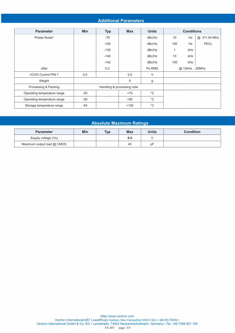
Parameter Min Typ Max Units ConditionsPhase Noise3 -75 dBc/Hz 10 Hz @ 311.04 MHz
-105 dBc/Hz 100 Hz PECL
-130 dBc/Hz 1 kHz
-140 dBc/Hz 10 kHz
-142 dBc/Hz 100 kHz
Jitter 0.2 Ps RMS @ 12kHz .. 20MHz
VCXO Control PIN 7 0,5 2,5 V
Weight 9 g
Processing & Packing Handling & processing note
Operating temperature range -20 +70 °C
Operating temperature range -30 +85 °C
Storage temperature range -55 +125 °C
Parameter Min Typ Max Units ConditionSupply voltage (Vs) 6.0 V
Maximum output load @ CMOS 40 pF
Additional Parameters
Absolute Maximum Ratings
FX-401 page: 3/8
htttp://www.vectron.comVectron International•267 LowellRoad, Hudson, New Hampshire 03051•Tel:+1-88-VECTRON-1
Vectron International GmbH & Co. KG • Landstraße, 74924 Neckarbischofsheim, Germany • Tel: +49 7268 801 100
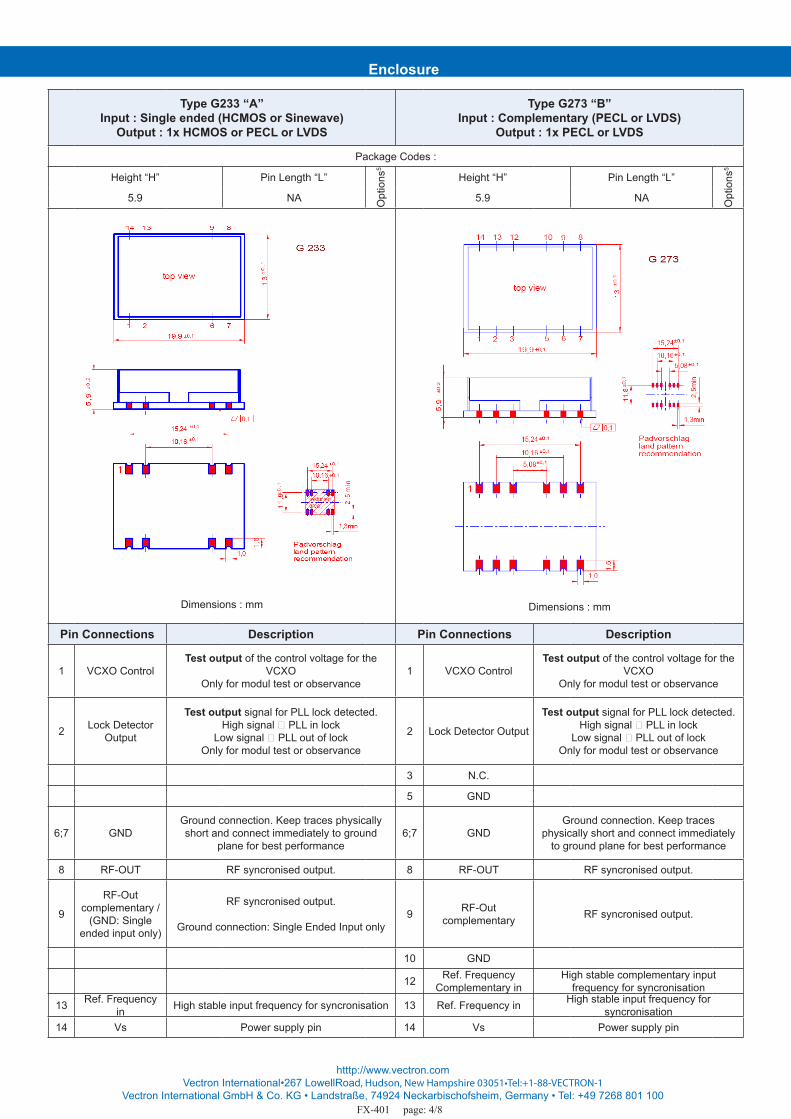
Enclosure
htttp://www.vectron.comVectron International•267 LowellRoad, Hudson, New Hampshire 03051•Tel:+1-88-VECTRON-1
Vectron International GmbH & Co. KG • Landstraße, 74924 Neckarbischofsheim, Germany • Tel: +49 7268 801 100
Type G233 “A”Input : Single ended (HCMOS or Sinewave)
Output : 1x HCMOS or PECL or LVDS
Type G273 “B”Input : Complementary (PECL or LVDS)
Output : 1x PECL or LVDS
Package Codes :
Height “H” Pin Length “L”
Opt
ions
5
Height “H” Pin Length “L”
Opt
ions
5
5.9 NA 5.9 NA
Dimensions : mm
Dimensions : mm
Pin Connections Description Pin Connections Description
1 VCXO ControlTest output of the control voltage for the
VCXO Only for modul test or observance
1 VCXO ControlTest output of the control voltage for the
VCXO Only for modul test or observance
2 Lock Detector Output
Test output signal for PLL lock detected. High signal PLL in lock
Low signal PLL out of lockOnly for modul test or observance
2 Lock Detector Output
Test output signal for PLL lock detected. High signal PLL in lock
Low signal PLL out of lockOnly for modul test or observance
3 N.C.
5 GND
6;7 GNDGround connection. Keep traces physically short and connect immediately to ground
plane for best performance6;7 GND
Ground connection. Keep traces physically short and connect immediately
to ground plane for best performance
8 RF-OUT RF syncronised output. 8 RF-OUT RF syncronised output.
9
RF-Out complementary /
(GND: Single ended input only)
RF syncronised output.
Ground connection: Single Ended Input only9 RF-Out
complementary RF syncronised output.
10 GND
12 Ref. Frequency Complementary in
High stable complementary input frequency for syncronisation
13 Ref. Frequency in High stable input frequency for syncronisation 13 Ref. Frequency in High stable input frequency for
syncronisation14 Vs Power supply pin 14 Vs Power supply pin
FX-401 page: 4/8

htttp://www.vectron.comVectron International•267 LowellRoad, Hudson, New Hampshire 03051•Tel:+1-88-VECTRON-1
Vectron International GmbH & Co. KG • Landstraße, 74924 Neckarbischofsheim, Germany • Tel: +49 7268 801 100
Enclosure
Type G273 “C”Input : Single ended (HCMOS or Sinewave)
Output : 2x PECL or LVDS
Type G267 “D”Input : Single ended (HCMOS or Sinewave)
Output : 4x HCMOS (same frequency)
Package Codes :
Height “H” Pin Length “L”
Opt
ions
5
Height “H” Pin Length “L”
Opt
ions
5
5.9 NA 5.9 NA
Dimensions : mm Dimensions : mm
Pin Connections Description Pin Connections Description
1 VCXO ControlTest output of the control voltage for the
VCXO Only for modul test or observance
1 VCXO ControlTest output of the control voltage for the
VCXO Only for modul test or observance
2 Lock Detector Output
Test output signal for PLL lock detected. High signal PLL in lock
Low signal PLL out of lockOnly for modul test or observance
2 Lock Detector Output
Test output signal for PLL lock detected. High signal PLL in lock
Low signal PLL out of lockOnly for modul test or observance
3 N.C.
5 GND 5 RF-OUT 1 4 independent RF syncronised outputs
6 RF-OUT 1 RF output frequency 1 6 GNDGround connection. Keep traces physically short and connect immediately to ground
plane for best performance
7 Compl. RF-OUT 1 Complimentary RF output frequency 1 7 RF-OUT 2 4 independent RF syncronised outputs
8 RF-OUT 2 RF output frequency 2 8 RF-OUT 3 4 independent RF syncronised outputs
9 Compl. RF-OUT 2 Complimentary RF output frequency 2 9 GND
10 GND 10 RF-OUT 4 4 independent RF syncronised outputs
12 N.C.
13 Ref. Frequency in High stable input frequency for syncronisation 13 Ref. Frequency in High stable input frequency for
syncronisation
14 Vs Power supply pin 14 Vs Power supply pin
FX-401 page: 5/8

MarkingFX-401
Frequency
AYYWW
(10 MHz; HCMOS output) (311,04 MHz; PECL output)
Frequency range [Hz] Jitter [ps rms] Frequency range [Hz] Jitter [ps rms]10Hz to 100kHz 0.708ps 12kHz to 20MHz 0.168ps
VS
8
15
4
0
8
15
4
VCXO
PLLCircuit
ReferenceFrequency VCXO
LockDetector
VCXOControl
0
VCXO
VS
VS
0
Loop Filter
VS
htttp://www.vectron.comVectron International•267 LowellRoad, Hudson, New Hampshire 03051•Tel:+1-88-VECTRON-1
Vectron International GmbH & Co. KG • Landstraße, 74924 Neckarbischofsheim, Germany • Tel: +49 7268 801 100
Typical Phase Noise and Jitter
Block Diagramm
Enclosure
FX-401 page: 6/8

*bei W ≤ 24 mm nur untere Lochreihe∗by W ≤ 24 mm only lower hole line
GurtoberseiteTape upper side
GurtunterseiteTape buttom side
AbwickelrichtungUnwinding direction
Lage im GurtPosition in tapePin 1A
X
P
B
K
Production tolerance complying DIN IEC 286-3
Enclosure Type Tape width W [mm] Quantity per meter Quantity per reel Dimension PG194B tbd tbd tbd tbd
Profile Feature Pb-Free Assembly/Sn-Pb Assembly Profile Feature Pb-Free Assembly/
Sn-Pb Assembly
Average ramp-up rate (TL to Tp) 3°C/second max. Time 25°C to Peak Temperature 8 minutes max.
Preheat -Temperature Min Tsmin -Temperature Min Tsmax -Time (min to max)(ts)
150°C200°C
60-180 seconds
Time maintainted above-Temperature (TL)
-Time (tL)217°C
60-150 seconds
Tsmax to TL-Ramp-up Rate 3°C/second max
Time maintainted above-Temperature (TL)
-Time (tL)217°C
60-150 seconds
Time within 5°C of actual Peak Temperature (tP) 20-40 seconds
Peak Temperature (TP) max 260°C Ramp-down Rate 6°C/ second max
Note: All temperatures refer to topside of the package, measured on the package body surface.SMD oscillators must be on the top side of the PCB during the reflow process.
Standard Shipping Methode (For B-Type Enclosure)
Recommanded Reflow Profile
htttp://www.vectron.comVectron International•267 LowellRoad, Hudson, New Hampshire 03051•Tel:+1-88-VECTRON-1
Vectron International GmbH & Co. KG • Landstraße, 74924 Neckarbischofsheim, Germany • Tel: +49 7268 801 100FX-401 page: 7/8

RF Output Code:A: HCMOSC: PECLD: LVDS
Height: 1: A 5,9 mm2: B 5,9 mm3: C 5,9 mm4: D 5,9 mm
Supply Voltage Code: E: 3,3 V
Temperature Range: H: -30...+85°C J: -20...+70°C
How to order this product:
Use this worksheet to forward the following information to your factory representative:
Model Height - Supply Voltage Code
RF Output Code
Temperature Range -
Reference Frequency - Output Frequency
FX-401 1 - E A J - -
htttp://www.vectron.comVectron International•267 LowellRoad, Hudson, New Hampshire 03051•Tel:+1-88-VECTRON-1
Vectron International GmbH & Co. KG • Landstraße, 74924 Neckarbischofsheim, Germany • Tel: +49 7268 801 100FX-401 page: 8/8