bulk zno nanorod assemblies fabricated by spin coating of organo-precursor gels on cuo nanowires
TRANSCRIPT

Materials Science-Poland, 31(3), 2013, pp. 397-403http://www.materialsscience.pwr.wroc.pl/DOI: 10.2478/s13536-013-0123-7
Bulk ZnO nanorod assemblies fabricated by spin coatingof organo-precursor gels on CuO nanowires
KASIMAYAN UMA1 , SOLIAPPAN ANATHAKUMAR2 , R. VISWANATH MANGALARAJA3 ,TETSUO SOGA1,4∗, TAKASHI JIMBO4
1Centre for Social Contribution and Collaboration, Nagoya Institute of Technology, Nagoya 466-85552Materials and Minerals Division, National Institute for Interdisciplinary Science and Technology (CSIR), Kerala, India
3Department of Materials Engineering, University of Concepcion, Concepcion, Chile4Department of Frontier Materials, Nagoya Institute of Technology, Nagoya, Japan
Bulk ZnO nanorod assemblies have been successfully fabricated on CuO nanowires through spin coating of organo-precursor gels. A thin film of CuO nanowires was first generated by direct heating of a metallic Cu-foil at 500 °C in anair atmosphere. A stable colloidal organo-precursor sol synthesized by dissolving equimolar zinc acetate dihydrate and mo-noethanolamine in 2-methoxyethanol was subsequently repeatedly deposited onto the CuO nanowires by spin coating. Theformation of ZnO nanorod assemblies was controlled by varying the number of coatings. The average diameter of the ZnO rodswas determined to be ∼ 600 nm.
Keywords: ZnO; CuO; sol-gel; Raman spectrum; SEM
© Wroclaw University of Technology.
1. Introduction
Nanostructured materials have attracted muchscientific attention due to their interesting size-dependent chemical and physical properties andpotential technological applications. Nanowiresand nanorods of various semiconducting materi-als, including Si, Ge, CuO, GaN, ZnO, SnO2, etc.have been synthesized for different potential appli-cations. Compared to the bulk materials, the ultra-fine materials reveal remarkable quantum effects,including electrical, optical and magnetic proper-ties that can be in principle tailored by varyingthe size. Zinc oxide (ZnO) is a fascinating, n-type II – VI semiconductor with a wide energyband gap (3.3 eV) and high exciton binding en-ergy (60 meV). It also exhibits high carrier mobil-ity and high transparency at room temperature. Dueto its almost indefinite stability and environmen-tally friendly properties, ZnO is recognized as a po-tential source for the fabrication of dye-sensitized
∗E-mail: [email protected]
solar cells and LEDs [1, 2]. Among the variousZnO nanostructures, ZnO nanorods and nanowiresare extremely important for the development of so-lar cells because they offer an increased interfacialarea and a direct path for the photo-generated elec-tron transport. However, an increased efficiency ispossible only when well-oriented ZnO nanorodsare fabricated. Therefore, active research is un-derway to synthesize the oriented semiconduct-ing ZnO nanostructures. One-dimensional ZnOnanostructures, including nanowires, nanobelts andnanotubes have been fabricated by vapor phaseevaporation [3], chemical vapor deposition [4], sol-gel [5], template method [6], laser ablation [7],and solution [8] processes. Most of these tech-niques are found to be successful for achieving bulknanostructures with randomly oriented nanowiresand rods.
Copper oxide (CuO) has been extensively stud-ied due to its suitability for the application in highTc superconductors and as a heterogeneous cata-lyst. Recently, CuO structures have found a vari-ety of applications in gas sensing [9], field emis-

398 KASIMAYAN UMA et al.
sion [10], and photovoltaic devices [11]. Cupric ox-ide is a p-type semiconductor with the band gapenergy between 1.96 and 2.38 eV. A solar cell as-sembly with high open-circuit voltage can be fab-ricated if a suitable n-type semiconductor is com-bined with CuO [12]. Since the 1950s, there hasbeen significant research into the growth of cop-per oxide whiskers and nanowires [13]. Solution-techniques [14], template assisted growth [15], andthermal oxidation of Cu metal [16] and Cu2S [17]are a few of the known techniques reported for thispurpose. The thermal oxidation process is remark-ably simple, because in this technique the growthof CuO whiskers/nanowires (100 – 200 nm) is ac-complished by the conventional heating of thickcopper sheets or foils at temperatures from 400 to700 °C in an ambient air environment. The thickcopper substrates effectively provide a large excessof copper during oxidative growth. In this work wehave attempted to fabricate bulk ZnO nanorod as-semblies on CuO nanowires. Here we report ona simple method for the fabrication of ZnO–CuOnanorods on Cu substrates by heating them in anair atmosphere. This is followed by the depositionof ZnO layers by the sol-gel spin coating method.SEM and Raman spectroscopy are employed toinvestigate the nanorod formation and the opticalproperties of the nanorods. The advantage of thistechnique is that it is simple and relatively inex-pensive to implement.
2. Experimental procedureMetallic copper foils, procured from Nilaco
Metals and Chemicals, Japan (1 cm × 1 cm, withthickness of 0.1 mm), were used as substrates forgrowing the CuO nanowires. The copper foil washeated in an electrical coiled furnace at 500 °C inair for 4 hours. Upon heating, the shiny copper sur-face turned black. A coating precursor solution wasprepared by dissolving zinc acetate di-hydrate (Zn(CH3COO)2·2H2O), Nacalai Tesque Chemical Co.Ltd., 99.5 %) and equivalent molar quantity of mo-noethanolamine (MEA, Nacalai Tesque ChemicalCo. Ltd., 99.5 %) in 2-methoxyethanol (NacalaiTesque Chemical Co. Ltd). The precursor solutionwas homogenously mixed by simple stirring for
3 hours at room temperature and then at 60 °C for2 hours. The precursor sol was deposited onto thepreheated copper foils by spin coating at 2000 rpmfor 20 seconds and then at 3000 rpm for another20 seconds at room temperature. Immediately afterthe coating, the precursor films were subjected tocuring at 300 °C for 10 min to remove the excesssolvents and residual moisture. The coating processwas repeated 2, 5 and 10 times. Finally, the coatedsubstrates were annealed at 600 °C for 2 h in air at-mosphere. Coatings were also prepared on the glassand silicon substrates under identical conditions forthe purpose of comparison. The as-prepared prod-ucts were observed and characterized by scanningelectron microscopy (SEM, S-3000H Hitachi), X-ray diffraction (X-ray diffractometer – JEOL) andRaman spectrometer (NRS 1500W Raman Spec-trometer – JASCO.
3. Results and discussion
3.1. XRD analysis
The X-ray diffraction analysis of the as receivedCu-foil, the Cu-foil thermally heated to 500 °C andthe ZnO precursor layers heated at 600 °C on Cufoil are presented in Fig. 1 (a – e). The as re-ceived Cu-foil shows two sharp crystalline peaksat 2θ = 43.46° and 50.6° that confirms that thefoils are phase-pure cubic-metallic Cu as shown inFig. 1(a). The diffraction peaks of thermally heatedCu-foil in Fig. 1(b) represent the fully crystallinemonoclinic CuO phase (JCPDS 48-1548) [18]. Inthis case, when copper is oxidized in air, Cu2O isinitially formed and then it transforms into CuOthrough secondary oxidation. The Cu2O actuallyserves as a precursor for obtaining CuO nanowires.The high vapor pressure of the bulk Cu-metal re-actants serves to accelerate the growth of the CuOnanowires [19]. We assume that the oxidation ofcopper to Cu2O and then to CuO provides the en-ergy required to form additional surfaces for thenanowires. Oxidation leads to stress in the foil dueto volume and structural changes. Sufficiently highrates of oxidation coupled with the low mobility ofatoms in the solid lead to relaxation of stress by theformation of small crystallites of CuO from which

Bulk ZnO nanorod assemblies fabricated by spin coating of organo-precursor gels. . . 399
Fig. 1. XRD analysis of: (a) pure Cu metal foil; (b) Cufoil heated at 500 °C in air; CuO nanowire sur-face with (c) two- (d) five- and (e) ten- coatingsof ZnO precursor sol.
the nanowires are observed to grow. Once the pre-cursor sol is coated, the lateral growth of the CuOnanowire is largely controlled. Fig. 1 (c – e) rep-resent the X-ray analysis of the ZnO coatings de-posited on the CuO thin films with different coat-ing layers. When the precursor sol is spin coatedtwice, the X-ray pattern exhibits peaks that corre-spond to only the CuO phase. However, a signifi-cant reduction in the peak intensity is observed dueto the double precursor coating. When the numberof deposition cycles is increased from two to five,a poorly crystalline, weak ZnO peak appears in thespectrum. A large amount of strong ZnO peaks areseen in the spectrum after ten coatings. The X-raypattern clearly shows that the diffraction peaks arevery intense, confirming that the coatings are fullycrystalline wurtzite ZnO. It is well known that tran-sition metal monoxides, like NiO, FeO, and CuO,which are similar to metal catalysts, have a goodcatalytic effect on the growth of semiconductornanoscale materials. Lyu et al. [20], for example,successfully synthesized ZnO nanowires on NiO-catalyzed alumina substrates. In our experiments,the copper oxide nanowires played a key role as acatalyst for the synthesis of the ZnO nanorods andmicrorods.
3.2. SEM analysisA SEM image of the Cu-foil heated at 500 °C is
shown in Fig. 2. At the given thermal heat treatment
conditions, the SEM image confirms that there isa bulk growth of CuO wires with the dimensionsof 100 – 300 nm in length and a maximum 10 µmin width. The microstructures of the ZnO coatingsgenerated on the CuO substrates at various timesof deposition are shown in Figs. 3(a), 4(a) and5(a). When the deposition is made only twice, thenanowire morphology collapses, and the basic mor-phology of the wire changes to become a rod-likestructure. The change in morphology is expectedwhen the precursor solution is deposited on thesubstrate surface, because, due to the large surfacearea of the CuO wires, the functional groups fromthe precursor solution, e.g, Zn, –OH and aminegroups, react with the Cu–O species. During sub-sequent heat treatment, the monoethanolamine dis-sociates into ammonia and hydroxyl groups on thesurface of ZnO induce hydrolytic reactions and fi-nally complex hydroxides are formed. The organo-precursor gel prepared in monoethanolamine is asomewhat viscous and hygroscopic medium andduring heating, apart from the hydrolysis, the ac-companying changes in the enthalpy and heat ca-pacity of the precursor gels lead to structural col-lapse of the wire structure. When the number ofspin coatings is increased to five, growth is predom-inant and the morphology is completely changedinto highly oriented rods. Since XRD patternsclearly show the presence of fully crystalline ZnO,we can confirm that they are ZnO rods. As ex-pected, the length of the rods is on the micronlevel, but the width is on the nanometer scale, and,interestingly, all the ZnO rods exhibit high degreeof uniformity in size and shape with a specific ori-entation. Due to its wurtzite structure, ZnO exhibitsa non-central symmetry and polar surfaces. The op-positely charged ions produce positively charged(0001)-Zn and negatively charged (0001)-O polarsurfaces, resulting in a normal dipole moment andspontaneous polarization along the c-axis, as wellas a divergence in surface energy. Due to such in-herent character of ZnO, the nucleation and growthwould preferably occur in one direction, leadingto rod-like growth. After 10 coating cycles, thecharacteristic structure of the ZnO rods collapsesand the morphology changes into a cage-like net-worked microstructure. However, in both cases, the

400 KASIMAYAN UMA et al.
coatings are very dense and the rod assembly istightly packed on the substrate surface. The growthof crystalline ZnO can also be attributed to the cat-alytic nature of the reactive CuO nanowires. This isconfirmed by deposition of the precursor solutionon the surface of the silicon substrates under iden-tical conditions (Figs. 3(b), 4(b) and 5(b)) and glass(Figs. 3(c), 4(c) and 5(c)). The growth of the ZnOnanorods can be attributed to the catalytic natureof the CuO layer. It is also seen that under iden-tical conditions, nanorods could not be producedwhen the precursor had been deposited on the glassand silicon substrates. The evolution of the mor-phologies of the precursor coatings on these sub-strates was observed by SEM, and revealed thatthe layers obtained after two deposition cycles con-tained mainly amorphous clusters of nano partic-ulate Zn-hydroxide phases. The gradual increasein the number of depositions only resulted in ag-glomerated particles. After ten deposition cycles,the coatings exhibited a cage like structures sim-ilar to the growth pattern obtained over the CuOnanowires. However, in none of these cases didZnO nanorods form. Apart from the catalytic char-acteristics of Cu–O, the whole structure of CuOwires can also be a possible reason for the orientedgrowth of ZnO. The bonding in CuO is partiallyionic and it has a monoclinic structure with 2hC6
symmetry. Every oxygen atom has four neighbor-ing copper atoms arrayed in a distorted tetrahedralconfiguration. In CuO there also exists a slightlydistorted planar square in the form of a parallelo-gram, formed by copper and oxygen atoms. Due tothis crystal nature, the ZnO growth is accelerated,particularly in the oriented directions.
3.3. Raman spectroscopy analysis
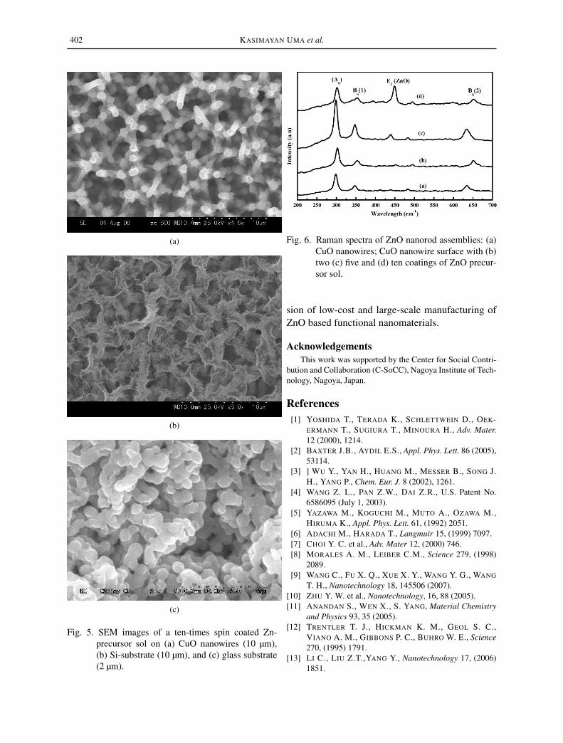
We have also confirmed by the Raman spec-troscopy that zinc is well incorporated into theCuO substrate. The Raman spectra of the CuO sub-strates containing ZnO-coatings and the CuO sub-strate without any coating are presented in Fig. 6.The plain CuO substrate shows three strong peaksat 286, 335 and 625 cm−1 and one weak peak at480 cm−1. This is attributed to the Ag, B(1)
g , and Bg
modes of the CuO due to the vibrations of the oxy-
Fig. 2. SEM (10 µm) image of CuO nanowires pre-pared by thermal activation of Cu metallic foilat 500 °C in an air atmosphere.
gen atoms [21]. When the ZnO layers are depositedover the substrate, the Raman spectrum gives asignal at 439 cm−1 and this peak corresponds tothe E2 mode of ZnO [22]. The presence of the E2mode in the Raman spectra of the samples confirmsthe wurtzite nature of the ZnO products. However,the distributions of CuO and ZnO are not uniformand obviously different Raman signals are obtainedfrom different regions. For the ZnO layer obtainedafter a ten time deposition, the spectrum shows theincreasing intensity of the E2 mode of ZnO. Theincreasing intensity of the E2 mode is due to thehighly crystalline structure of the ZnO crystal.
4. ConclusionsIn conclusion, ZnO nanorods have been suc-
cessfully grown on the CuO nanowires derivedfrom metallic Cu-substrates. When the zinc con-taining organo-precursor sol was deposited over theCu- substrate surface by spin coating, a dense, fullycrystalline ZnO nanorod assembly was achieved at600 °C. However, the coating process must havebeen repeated more than five times. The growthof the ZnO nanorods can be attributed to the cat-alytic nature of the CuO layer. We also observedthat under identical conditions, nanorods could notbe produced when the precursor was deposited onglass and silicon substrates. This controlled synthe-sis has good potential to be scaled-up for the provi-

Bulk ZnO nanorod assemblies fabricated by spin coating of organo-precursor gels. . . 401
(a)
(b)
(c)
Fig. 3. SEM images of a two-times spin coated Zn-precursor sol on: (a) CuO nanowires (5 µm),(b) Si-substrate (10 µm) and (c) glass substrate(2 µm).
(a)
(b)
(c)
Fig. 4. SEM images of a five-times spin coated Zn-precursor sol on: (a) CuO nanowires (10 µm),(b) Si-substrate (2.5 µm) and (c) glass substrate(5 µm).
402 KASIMAYAN UMA et al.
(a)
(b)
(c)
Fig. 5. SEM images of a ten-times spin coated Zn-precursor sol on (a) CuO nanowires (10 µm),(b) Si-substrate (10 µm), and (c) glass substrate(2 µm).
Fig. 6. Raman spectra of ZnO nanorod assemblies: (a)CuO nanowires; CuO nanowire surface with (b)two (c) five and (d) ten coatings of ZnO precur-sor sol.
sion of low-cost and large-scale manufacturing ofZnO based functional nanomaterials.
AcknowledgementsThis work was supported by the Center for Social Contri-
bution and Collaboration (C-SoCC), Nagoya Institute of Tech-nology, Nagoya, Japan.
References[1] YOSHIDA T., TERADA K., SCHLETTWEIN D., OEK-
ERMANN T., SUGIURA T., MINOURA H., Adv. Mater.12 (2000), 1214.
[2] BAXTER J.B., AYDIL E.S., Appl. Phys. Lett. 86 (2005),53114.
[3] ] WU Y., YAN H., HUANG M., MESSER B., SONG J.H., YANG P., Chem. Eur. J. 8 (2002), 1261.
[4] WANG Z. L., PAN Z.W., DAI Z.R., U.S. Patent No.6586095 (July 1, 2003).
[5] YAZAWA M., KOGUCHI M., MUTO A., OZAWA M.,HIRUMA K., Appl. Phys. Lett. 61, (1992) 2051.
[6] ADACHI M., HARADA T., Langmuir 15, (1999) 7097.[7] CHOI Y. C. et al., Adv. Mater 12, (2000) 746.[8] MORALES A. M., LEIBER C.M., Science 279, (1998)
2089.[9] WANG C., FU X. Q., XUE X. Y., WANG Y. G., WANG
T. H., Nanotechnology 18, 145506 (2007).[10] ZHU Y. W. et al., Nanotechnology, 16, 88 (2005).[11] ANANDAN S., WEN X., S. YANG, Material Chemistry
and Physics 93, 35 (2005).[12] TRENTLER T. J., HICKMAN K. M., GEOL S. C.,
VIANO A. M., GIBBONS P. C., BUHRO W. E., Science270, (1995) 1791.
[13] LI C., LIU Z.T.,YANG Y., Nanotechnology 17, (2006)1851.

Bulk ZnO nanorod assemblies fabricated by spin coating of organo-precursor gels. . . 403
[14] ZHANG K, ROSSI C., ARDILA G. A., RODRIGUEZ R.,TENAILEAU C., ALPHONSE P., Appl. Phys. Lett. 91,(2007) 113117.
[15] CHALTYKYAN O. A., Copper-catalytic Reactions, Con-sultants Bureau, New York, NY, USA, 1966.
[16] HOMMA T., ISSIKI S., Acta Metall. 12, (1964) 1092.[17] WANG W. Z., WANG G. H., WANG X. S., ZHAN Y. J.,
LIU Y. K., ZHENG C. L., Adv. Mater 14, 6 (2002) 7.[18] HSIEH C. T., CHEN J. M., LIN H. H, SHIH H. C.,
Appl. Phys. Lett. 82, (2003) 3316.
[19] JIANG K., HERRICKS T., XIA Y., Nano. Lett. 2 812,(2002) 1333.
[20] WANG S., HUANG Q., WEN X., LI. X. AND YANG S.,Phys. Chem. 4, (2002) 3425-3430.
[21] ZHU Y. W. et al., Nanotechnology 16, (2005) 88.[22] ZONG B. et al., Chem. Mater. 17, (2005) 1515.
Received 2011-01-07Accepted 2013-05-22