buck voltage regulator using the pm8903 - st.com · where Δil is the voltage across the inductor...
TRANSCRIPT

June 2012 Doc ID 023053 Rev 1 1/11
AN4086Application note
Buck voltage regulator using the PM8903
By David Toland
IntroductionThe PM8903 is a compact, high-efficiency, monolithic step-down switching voltage regulator which can deliver up to 3 A of continuous current. The IC minimizes external components and board space by incorporating low-resistance MOSFETs into the IC. It is used in applications including CPU, DSP and FPGA power supplies, distributed power supplies, and for general DC/DC converters. The following features are incorporated:
■ Input voltage range of 2.8 V to 6 V
■ Adjustable output voltage to as low as 0.6 V
■ PSKIP mode for optimizing efficiency at light load
■ Undervoltage, overvoltage, overcurrent, and overtemperature protection
■ Power Good output
■ 1.1 MHz switching frequency which enables the use of a small inductor
■ Low quiescent current when shut down (<15 µA)
■ Interleaving synchronization (up to two ICs)
■ Small VFQFPN16, 3x3 mm package
www.st.com
Contents AN4086
2/11 Doc ID 023053 Rev 1
Contents
1 Circuit description . . . . . . . . . . . . . . . . . . . . . . . . . . . . . . . . . . . . . . . . . . . 4
2 Revision history . . . . . . . . . . . . . . . . . . . . . . . . . . . . . . . . . . . . . . . . . . . 10
AN4086 List of figures
Doc ID 023053 Rev 1 3/11
List of figures
Figure 1. PM8903 schematic . . . . . . . . . . . . . . . . . . . . . . . . . . . . . . . . . . . . . . . . . . . . . . . . . . . . . . . . 6Figure 2. R/C snubber circuit . . . . . . . . . . . . . . . . . . . . . . . . . . . . . . . . . . . . . . . . . . . . . . . . . . . . . . . . 6Figure 3. PM8903 demonstration board . . . . . . . . . . . . . . . . . . . . . . . . . . . . . . . . . . . . . . . . . . . . . . . 7Figure 4. PM8903 demonstration board efficiency with VIN = 3.3 V, VOUT = 1.5 V, and
FSW = 1.1 MHz . . . . . . . . . . . . . . . . . . . . . . . . . . . . . . . . . . . . . . . . . . . . . . . . . . . . . . . . . . 7Figure 5. Startup . . . . . . . . . . . . . . . . . . . . . . . . . . . . . . . . . . . . . . . . . . . . . . . . . . . . . . . . . . . . . . . . . 8Figure 6. VOUT, VIN, IIN ripple . . . . . . . . . . . . . . . . . . . . . . . . . . . . . . . . . . . . . . . . . . . . . . . . . . . . . . . 8Figure 7. Transient load (0 A to 1.5 A) . . . . . . . . . . . . . . . . . . . . . . . . . . . . . . . . . . . . . . . . . . . . . . . . . 8Figure 8. Transient load (1.5 A to 3 A) . . . . . . . . . . . . . . . . . . . . . . . . . . . . . . . . . . . . . . . . . . . . . . . . . 8Figure 9. Duty cycle jitter at 3 A load . . . . . . . . . . . . . . . . . . . . . . . . . . . . . . . . . . . . . . . . . . . . . . . . . . 8Figure 10. VOUT, VIN, IIN ripple . . . . . . . . . . . . . . . . . . . . . . . . . . . . . . . . . . . . . . . . . . . . . . . . . . . . . . . 8Figure 11. Overvoltage protection . . . . . . . . . . . . . . . . . . . . . . . . . . . . . . . . . . . . . . . . . . . . . . . . . . . . . 9Figure 12. Shutdown . . . . . . . . . . . . . . . . . . . . . . . . . . . . . . . . . . . . . . . . . . . . . . . . . . . . . . . . . . . . . . . 9

Circuit description AN4086
4/11 Doc ID 023053 Rev 1
1 Circuit description
● Output voltage setting
In Equation 1 below, the output voltage is programmed by ROS and RFB using the formula:
Equation 1
where VREF is 0.6 V and RFB is selected to obtain the desired regulator bandwidth (see section 6.1 of datasheet for details).
● Inductor selection
Choosing an inductor involves a compromise between dynamic response, efficiency, cost and size. A higher inductor value will decrease the output voltage ripple, but will increase the regulator response time to load changes.
The inductance has to be calculated to keep the ripple current (ΔIL) between 20% and 30% of the maximum output current, using the following equation:
Equation 2
where FSW is the switching frequency, VIN is the input voltage, and VOUT is the output voltage.
● Output capacitor selection
The output capacitor bank will define the ripple voltage and affect the transient response of the regulator.
During steady state operation, the output voltage ripple is affected by the ESR and the capacitance value according to the following equations:
Equation 3
Equation 4
where ΔIL is the inductor current ripple.
ROS = RFB * VREF / (VOUT – VREF)

AN4086 Circuit description
Doc ID 023053 Rev 1 5/11
During a load transient, the output capacitor bank either supplies the load current, or absorbs the energy stored in the inductor until the regulator reacts. The output voltage drop that depends on the ESR (equivalent series resistance) and on the capacitive charge/discharge is calculated according to the following:
Equation 5
where ΔIL is the voltage across the inductor during the transient load [DMAX · (VIN - VOUT) for a load application or VOUT for load release.
MLCC capacitors typically have low ESR which is good to minimize the voltage ripple, but they have low capacitance. Electrolytic capacitors have larger capacitance, which is good for minimizing voltage changes during transients, but they also have higher ESR than MLCC capacitors.
Ideally, a mix of electrolytic and MLCC capacitors can be used for minimal ripple as well as minimizing voltage changes during transient loads.
● Input capacitor selection
The major consideration when choosing an input capacitor is the input RMS current, which depends on the output current (IOUT) and the duty cycle (D) according to the following:
Equation 6
Maximum IRMS occurs when D = 0.5, when .
Make sure the capacitor RMS current rating is well above the maximum operating RMS current of the regulator. For long-term reliability, a good rule of thumb is to choose a capacitor that will exhibit less than a 10 °C rise in temperature at max RMS current. Most capacitor datasheets have plots that show RMS current vs. temperature.
Another consideration is the input ripple voltage - which is caused by the ESL (equivalent series inductance) and ESR of the input capacitor and the dV/dt of the switch node. Using low ESR and ESL ceramic capacitors are effective for lowering input ripple voltage.
IRMS IOUT D 1 D–( )⋅⋅=
IRMSIOUT
2------------=

Circuit description AN4086
6/11 Doc ID 023053 Rev 1
Figure 1. PM8903 schematic
● Design tip for input voltages of 5 V to 6 V
For a 5 V input, the maximum rated voltage at the phase pin is 7 V. For a 6 V input, the maximum rated voltage is 7.5 V with t < 100 ns.
If you use a 5 V to 6 V input voltage, the maximum voltage at the phase node should be measured at maximum load. This measurement should be taken on the phase node pin, using the full bandwidth setting on the oscilloscope and as short a ground as possible on the probe. If measured voltage exceeds 7 V, an R/C snubber circuit should be implemented at the phase node, as shown in Figure 2. Also, to be effective, the R/C should be as close as possible to the phase node pin.
Figure 2. R/C snubber circuit
AN4086 Circuit description
Doc ID 023053 Rev 1 7/11
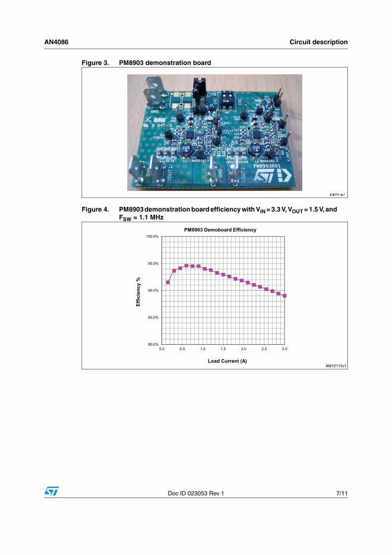
Figure 3. PM8903 demonstration board
Figure 4. PM8903 demonstration board efficiency with VIN = 3.3 V, VOUT = 1.5 V, and FSW = 1.1 MHz
Circuit description AN4086
8/11 Doc ID 023053 Rev 1
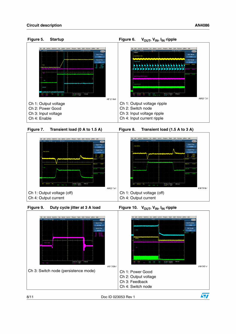
Figure 5. Startup Figure 6. VOUT, VIN, IIN ripple
Ch 1: Output voltageCh 2: Power GoodCh 3: Input voltageCh 4: Enable
Ch 1: Output voltage rippleCh 2: Switch nodeCh 3: Input voltage rippleCh 4: Input current ripple
Figure 7. Transient load (0 A to 1.5 A) Figure 8. Transient load (1.5 A to 3 A)
Figure 9. Duty cycle jitter at 3 A load Figure 10. VOUT, VIN, IIN ripple
Ch 1: Output voltage (off)Ch 4: Output current
Ch 1: Output voltage (off)Ch 4: Output current
Ch 3: Switch node (persistence mode) Ch 1: Power GoodCh 2: Output voltageCh 3: FeedbackCh 4: Switch node

AN4086 Circuit description
Doc ID 023053 Rev 1 9/11
Figure 11. Overvoltage protection Figure 12. Shutdown
Ch 1: Power GoodCh 2: Output voltageCh 3: Input voltageCh 4: Switch node
Ch 1: Output voltageCh 2: Power GoodCh 3: Input voltageCh 4: Enable
Revision history AN4086
10/11 Doc ID 023053 Rev 1
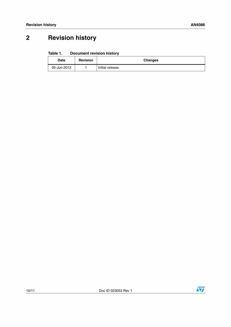
2 Revision history
Table 1. Document revision history
Date Revision Changes
05-Jun-2012 1 Initial release.
AN4086
Doc ID 023053 Rev 1 11/11
Please Read Carefully:
Information in this document is provided solely in connection with ST products. STMicroelectronics NV and its subsidiaries (“ST”) reserve theright to make changes, corrections, modifications or improvements, to this document, and the products and services described herein at anytime, without notice.
All ST products are sold pursuant to ST’s terms and conditions of sale.
Purchasers are solely responsible for the choice, selection and use of the ST products and services described herein, and ST assumes noliability whatsoever relating to the choice, selection or use of the ST products and services described herein.
No license, express or implied, by estoppel or otherwise, to any intellectual property rights is granted under this document. If any part of thisdocument refers to any third party products or services it shall not be deemed a license grant by ST for the use of such third party productsor services, or any intellectual property contained therein or considered as a warranty covering the use in any manner whatsoever of suchthird party products or services or any intellectual property contained therein.
UNLESS OTHERWISE SET FORTH IN ST’S TERMS AND CONDITIONS OF SALE ST DISCLAIMS ANY EXPRESS OR IMPLIEDWARRANTY WITH RESPECT TO THE USE AND/OR SALE OF ST PRODUCTS INCLUDING WITHOUT LIMITATION IMPLIEDWARRANTIES OF MERCHANTABILITY, FITNESS FOR A PARTICULAR PURPOSE (AND THEIR EQUIVALENTS UNDER THE LAWSOF ANY JURISDICTION), OR INFRINGEMENT OF ANY PATENT, COPYRIGHT OR OTHER INTELLECTUAL PROPERTY RIGHT.
UNLESS EXPRESSLY APPROVED IN WRITING BY TWO AUTHORIZED ST REPRESENTATIVES, ST PRODUCTS ARE NOTRECOMMENDED, AUTHORIZED OR WARRANTED FOR USE IN MILITARY, AIR CRAFT, SPACE, LIFE SAVING, OR LIFE SUSTAININGAPPLICATIONS, NOR IN PRODUCTS OR SYSTEMS WHERE FAILURE OR MALFUNCTION MAY RESULT IN PERSONAL INJURY,DEATH, OR SEVERE PROPERTY OR ENVIRONMENTAL DAMAGE. ST PRODUCTS WHICH ARE NOT SPECIFIED AS "AUTOMOTIVEGRADE" MAY ONLY BE USED IN AUTOMOTIVE APPLICATIONS AT USER’S OWN RISK.
Resale of ST products with provisions different from the statements and/or technical features set forth in this document shall immediately voidany warranty granted by ST for the ST product or service described herein and shall not create or extend in any manner whatsoever, anyliability of ST.
ST and the ST logo are trademarks or registered trademarks of ST in various countries.
Information in this document supersedes and replaces all information previously supplied.
The ST logo is a registered trademark of STMicroelectronics. All other names are the property of their respective owners.
© 2012 STMicroelectronics - All rights reserved
STMicroelectronics group of companies
Australia - Belgium - Brazil - Canada - China - Czech Republic - Finland - France - Germany - Hong Kong - India - Israel - Italy - Japan - Malaysia - Malta - Morocco - Philippines - Singapore - Spain - Sweden - Switzerland - United Kingdom - United States of America
www.st.com