bringing up a chip on the cheap -...
TRANSCRIPT

Bringing Up a Chip onthe CheapMegan Wachs, Ofer Shacham, Zain Asgar,
Amin Firoozshahian, Stephen Richardson, and
Mark Horowitz
Stanford University
h ‘‘CONGRATULATIONS, IT’S A . . . chip!’’ Much like
real babies, a newly born chip starts its life helpless,
and (unfortunately) much like a real baby, it takes
significant work to nurture the chip until it takes its
first step; and even more work getting it to run real
applications as a mature adult. Anyone who ever
built a chip knows that tapeout is never the end. In
some ways, it’s just the beginning. After fabrication,
the chip must be ‘‘booted’’ on some kind of real
system, to verify correct functionality. This bringup
process is expensive and time-consuming, as well as
something of a distraction for the validation team,
who truly wish(ed) that tapeout really was the end
of the process. In addition, the bringup of any chip,
especially a test chip, can only be allocated limited
resources.
This paper describes one team’s experience
bringing up a research chip: Stanford Smart Mem-
ories (SSM). This chip was designed and validated
by a very small team, although as an 8-core, recon-
figurable chip multiprocessor with 55 million tran-
sistors, it was by no means a simple chip. The design
of this substantial chip took several years, and by
tapeout, its supporting
research contract had ex-
pired, resulting in ex-
tremely limited funds for
implementing the postsili-
con processes. Testability
of the chip was considered
from the beginning, and
the team implemented
several well-known industry techniques to aid post-
silicon debugging. However, our team had to look
for a creative solution for the bringup platform. For-
tunately, an early design choice had us use an estab-
lished processor from Tensilica as the chip’s core
compute engine, one with solid built-in debugging
support. We then found creative ways to leverage
Berkeley’s BEE2 FPGA platform [2] as a generic
means for system testing, even though it was never
intended for bringup. By using this commodity
hardware supplemented by a very simple daughter
card, the bringup tasks were achievable by 1-2 grad
students working part time. The bringup process,
from getting silicon in hand to having it run system-
level programs (SPLASH-2 [2] kernels running on
multiple processors) took only about a month. A 32-
processor system of four chips has been successfully
constructed using the same platform.
While industrial designs may have more re-
sources and need for a custom testing platform
(especially since the design is likely to be part of at
least one commercial product), this paper is de-
signed to provide encouragement, advice, and pitfall
lessons for teams desiring to bring up a chip quickly,
with minimum custom hardware (i.e. on the cheap).
Section II briefly describes the SSM chip, while
Section III explains how we planned for bringup
Editor’s notes:Booting and debugging the functionality of silicon samples are known to bechallenging and time-consuming tasks, even more so in cost-constrainedenvironments. The authors describe their creative solutions used to bring upStanford Smart Memories (SSM), a 55-million transistor research chip.
VNicola Nicolici, McMaster University
0740-7475/12/$31.00 B 2012 IEEENovember/December 2012 Copublished by the IEEE CEDA, IEEE CASS, IEEE SSCS, and TTTC 1
Digital Object Identifier 10.1109/MDT.2011.2179849
Date of publications: 00 Month 0000.

during RTL design. Section IV describes our bringup
platform and tells our bringup story. Section V ana-
lyzes the utility of the various debugging features.
The smart memories chipThe Stanford Smart Memories (SSM) research
project [4]–[8] aimed to build a hardware platform
supporting multiple programming models by relying
on a flexible execution and memory system archi-
tecture. Each SSM chip contains eight Tensilica pro-
cessors, several modular reconfigurable memory
blocks, and a programmable protocol controller. An
off-chip interconnection network joins the chips to
main-memory controllers (MC). RTL for MCs and
network switches (NS) was to be implemented as
separate board-level glue logic. System simulation
integrated four SSM chips with RTL versions of
1-4 MCs and an NS to provide 32-core functionality.
SSM’s software includes a C/C++ Tensilica compiler
instrumented with special Tensilica Instruction
Extension (TIE) instructions. SSM taped out as an
eight-core chip multiprocessor in late 2008. ST-
Microelectronics fabricated the 61 mm2 silicon
chip in 90 nm technology, shown in Figure 1a.
Designing for bringupLong before tapeout, we considered the bringup
process to ensure that when the chip returned from
fabrication, we could debug any failures. Designers
in industry and academia have long addressed the
same challenge ([3]–[12], to name a few). The
SSM’s design originally involved a custom processor
called Imagine, in development by another Stanford
group. For practical reasons, we instead chose to use
Tensilica, an established processor with debugging
support. We leveraged Tensilica’s on-chip debugger
(OCD), controlled via industry-standard JTAG (IEEE
Std. 1149.1-2001), by concatenating the processors’
JTAG chains (see Figure 2). OCD enables using stan-
dard tools like gdb after tapeout. In addition, we
mapped the processors’ debug trace ports to confi-
guration registers, accessible via processor or JTAG
reads.
To read/write the SSM configuration, debug, and
on-chip memory space, we added a ninth JTAG
controller at the chip level. Extensive JTAG simula-
tions ensured that it could load programs into on-
chip memories, configure the system, and run tests
without a more sophisticated platform. The JTAG
interface also enabled boundary scan for EXTEST
and SAMPLE testing, as well as full scan.
Special consideration was given to the power-on/
reset sequence, as this can be Achilles’ heel of any
design, especially a reconfigurable design. Two sig-
nals, Reset and DisableBootProc, control SSM’s confi-
guration and boot sequence. With DisableBootProc
in its normal OFF position, a positive edge on Reset
places SSM in its default configuration and starts one
processor. This processor can further configure the
chip and bring other processors out of reset. With
DisableBootProc ON, however, posedge Reset still
configures the chip, but nothing runs. In this state,
JTAG can configure the chip and bring processors
out of reset via configuration writes.
SSM also had a significant amount of statistic-
gathering support. It supported extensive logging for
Figure 1. (a) Die photograph of the 61 mm2, 55M-transistor SSM chip fabricated in 90 nm technology.Each chip includes eight Tensilica processors, 64 KB of local configurable memory, and a memorysystem with programmable protocol controller. (b) Simple riser card, used to connect a BEE2 DIMMsocket to an SSM daughter card. (c) and (d) Custom daughter cards, with soldered chip and with asocket (respectively). (e) A complete system mounted on the BEE2 platform. Silicon bringup includedtesting of 1–32 processor systems (up to four SSM chips as shown).
IEEE Design & Test of Computers2
General Interest

performance information at several levels, and
could be configured to record four instruction-level
traces into on-chip memory. Compressed, these
traces can record up to 4K instruction branches
for each processor. Several registers on the chip
(accessible via processor or JTAG reads) mapped to
debugging information, such as each processor’s
current PC, stall state, etc. As a final window into a
nonresponsive chip, a dedicated set of 12 output
pins connected to key internal signals (such as
resets and actively monitored processor clocks),
similar to the ‘‘Observability Bus’’ in [7]. An input-
controlled multiplexer selected between 32 vectors,
unconstrained by timing, because they would only
be observed with a slow clock.
Before committing to tapeout, we had to design a
platform that would communicate with our chip. To
reduce the probability of error from reasons unre-
lated to our research goals, excess features were
relegated to ‘‘the FPGA,’’ the mythical device that
would allow SSM to communicate with the outside
world. For example, an abstract flit-based network
interface replaced an on-chip memory controller,
synchronized by an I/O clock divisible by 1-8 relative
to the core clock. The FPGA would implement our
MC as well as provide access to a 3-GB memory
space. Vermuelen and Goel [10] consider using the
application board to do all this, but our bringup
system had to avoid custom hardware. This was to
reduce costs, but also because such work was out-
side of the research goalsVit was overhead that
could only lead to student burnout.
Since we had already emulated our design with a
Berkeley BEE2 [2] board, we decided to use the
BEE2’s FPGAs to implement the glue logic for bring-
up, as shown in Figure 3. The FPGA’s PowerPC served
as a host, allowing us to connect via BEE2’s Ethernet
port and run tests remotely. This scheme required a
way to connect the SSM chip to the BEE2 board.
Unfortunately, the BEE2 was not designed to be
extensible and had limited I/O.
After struggling with the SSM’s I/O requirements
and considering the BEE2’s low I/O counts, we
arrived at a solution: remove two DDR2 DIMM cards
from the BEE2 board, and use the over 200 available
DDR signals to communicate with SSM. For elec-
trical signal integrity reasons, the connections had
to be terminated (with 50�, resistors to prevent
reflections)Vthey were. Each also needed to be an
independent signal lineVmost were. SPICE simula-
tions ensured that BEE2 signal levels were compat-
ible with an SSM’s 1.8 V I/O level. A few more sanity
checks convinced us that this would be a viable
solution. Using half of the DIMM slots in this way,
however, limited the platform to 2 GB of memory,
which would be partitioned between the host
PowerPC (which controls the platform) and the
MC (part of the system under test). Therefore, a
memory translation block was inserted between the
MC and the true DDR2 controller (see Figure 3). This
single-cycle latency block mapped twelve 0.25 GB
memory segments, covering SSM’s address space
from 1 GB-4 GB (SSM did not use off-chip addresses
below 1 GB). SSM memory accesses included both
meta-data and data, so fully mapping a 0.25 GB
address range required 0.5 GB of DDR memory. Each
SSM segment could map to a 64-512 MB DDR block,
specified by starting address and size. If a processor
accessed an address that was too high, the behavior
would be erroneous, but we controlled the compiler
and ensured that each instruction, data, stack etc.
region did not exceed its segment size. The transla-
tion block also checked for overflow. A commercial
chip could warrant a custom platform with dedi-
cated I/O connections, but this design allowed us to
Figure 2. Schematic representation of theSSM chip showing the tiled processorsand the protocol controller, with the serialconnection of JTAG test access ports(TAPs). Each Tensilica processor has a TAPto control its on-chip debugger. These werestitched with the chip level TAP, whichcontrolled the configuration registers,accessed the on-chip memory space, andhandled the scan chains.
November/December 2012 3
proceed to tapeout without constructing a custom
test rig.
Bringup system and flowWith the BEE2 as a commodity platform, we
could push a significant amount of support functio-
nality onto the FPGAs, requiring only a simple board
to hold SSM. After exploring several DIMM socket
connection options, we created custom riser cards
(see Figure 1b), to both physically support the
daughter card above the FPGAs, and transmit signals.
The custom daughter card (see Figures 1c and
1d) holding SSM had few components. Manual
switches controlled some signals (ChipID, Debug-
MuxSel, TestMode, ScanEn, IODiv, DisableBootProc,
and Reset). The FPGA could also control most of
these, to allow remote testing. A JTAG connector on
the daughter card allowed quick standalone testing,
but we also routed the JTAG sig-
nals with the flit signals through
the riser cards to the FPGA.
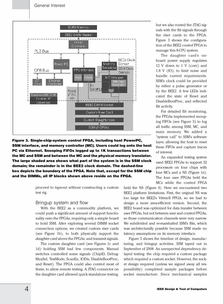
Figure 3 shows the configura-
tion of the BEE2 control FPGA to
manage this 8-CPU system.
The daughter card’s on-
board power supply regulates
12 V down to 1 V (core) and
1.8 V (IO), to limit noise and
handle current requirements.
SSM’s clock could be provided
by either a pulse generator or
by the BEE2. A few LEDs indi-
cated the state of Reset and
DisableBootProc, and reflected
flit activity.
For detailed flit monitoring,
the FPGAs implemented snoop-
ing FIFOs (see Figure 3) to log
all traffic among SSM, MC, and
main memory. We added a
‘‘system call’’ to SSM’s software
layer, allowing the host to reset
these FIFOs and capture traces
of interest.
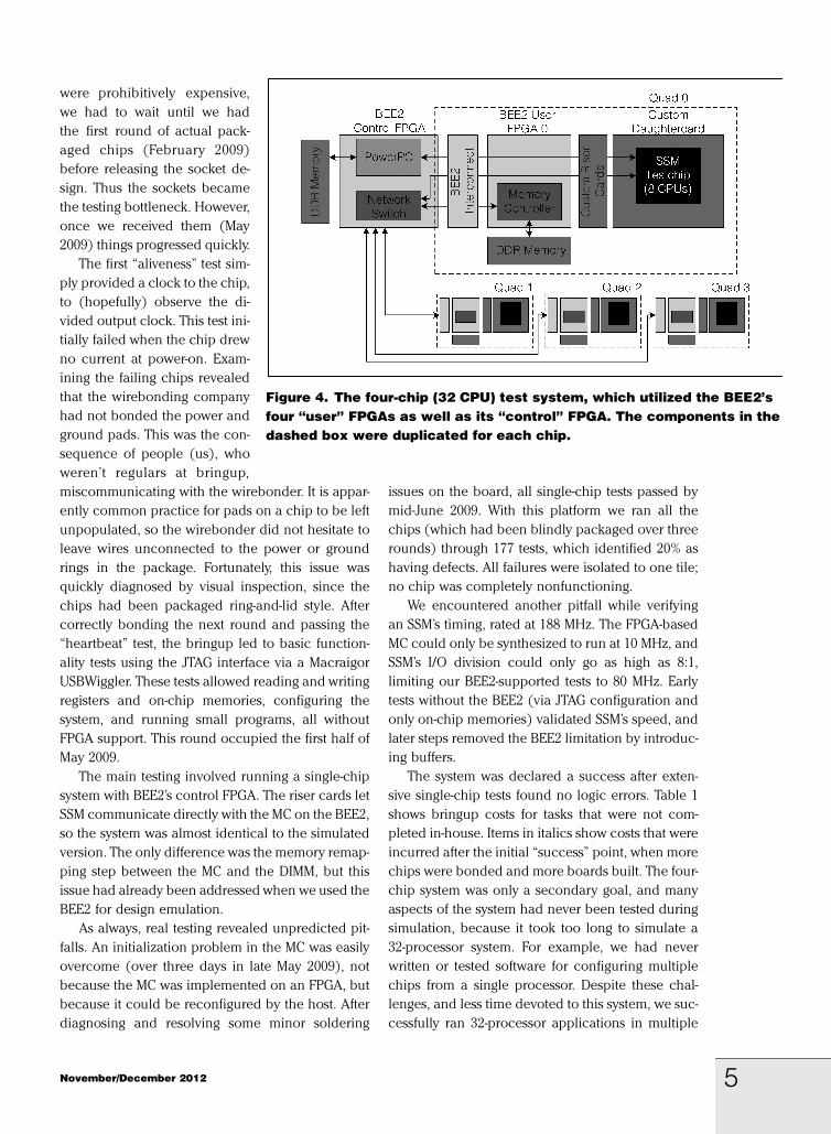
An expanded testing system
used BEE2 FPGAs to support 32
processors on four chips with
four MCs and a NS (Figure 1e).
The four user FPGAs held the
MCs while the control FPGA
held the NS (Figure 4). Here we encountered two
BEE2 platform limitations. First, the original NS was
too large for BEE2’s Virtex-II FPGA, so we had to
design a more area-efficient version. Second, the
BEE2 board was optimized for data transfer between
user FPGAs, but not between user and control FPGAs,
so those communication channels were very narrow.
We subdivided and re-marshalled SSM’s flits, which
was architecturally possible because SSM made no
latency assumptions on its memory interface.
Figure 5 shows the timeline of design, manufac-
turing, and bringup activities. SSM taped out in
September of 2008. An unexpected dependency de-
layed testing: the chip required a custom package
which required a custom socket. However, the sock-
et design required (unless we signed away all res-
ponsibility) completed sample packages before
socket manufacture. Since mechanical samples
Figure 3. Single-chip-system control FPGA, including host PowerPC,SSM interface, and memory controller (MC). Users could log onto the hostPC via Ethernet. Snooping FIFOs logged up to 1K transactions betweenthe MC and SSM and between the MC and the physical memory translator.The large shaded area shows what part of the system is in the SSM clockdomain; the remainder is in the BEE2 clock domain. The dashed-linebox depicts the boundary of the FPGA. Note that, except for the SSM chipand the DIMMs, all IP blocks shown above reside on the FPGA.
IEEE Design & Test of Computers4
General Interest
were prohibitively expensive,
we had to wait until we had
the first round of actual pack-
aged chips (February 2009)
before releasing the socket de-
sign. Thus the sockets became
the testing bottleneck. However,
once we received them (May
2009) things progressed quickly.
The first ‘‘aliveness’’ test sim-
ply provided a clock to the chip,
to (hopefully) observe the di-
vided output clock. This test ini-
tially failed when the chip drew
no current at power-on. Exam-
ining the failing chips revealed
that the wirebonding company
had not bonded the power and
ground pads. This was the con-
sequence of people (us), who
weren’t regulars at bringup,
miscommunicating with the wirebonder. It is appar-
ently common practice for pads on a chip to be left
unpopulated, so the wirebonder did not hesitate to
leave wires unconnected to the power or ground
rings in the package. Fortunately, this issue was
quickly diagnosed by visual inspection, since the
chips had been packaged ring-and-lid style. After
correctly bonding the next round and passing the
‘‘heartbeat’’ test, the bringup led to basic function-
ality tests using the JTAG interface via a Macraigor
USBWiggler. These tests allowed reading and writing
registers and on-chip memories, configuring the
system, and running small programs, all without
FPGA support. This round occupied the first half of
May 2009.
The main testing involved running a single-chip
system with BEE2’s control FPGA. The riser cards let
SSM communicate directly with the MC on the BEE2,
so the system was almost identical to the simulated
version. The only difference was the memory remap-
ping step between the MC and the DIMM, but this
issue had already been addressed when we used the
BEE2 for design emulation.
As always, real testing revealed unpredicted pit-
falls. An initialization problem in the MC was easily
overcome (over three days in late May 2009), not
because the MC was implemented on an FPGA, but
because it could be reconfigured by the host. After
diagnosing and resolving some minor soldering
issues on the board, all single-chip tests passed by
mid-June 2009. With this platform we ran all the
chips (which had been blindly packaged over three
rounds) through 177 tests, which identified 20% as
having defects. All failures were isolated to one tile;
no chip was completely nonfunctioning.
We encountered another pitfall while verifying
an SSM’s timing, rated at 188 MHz. The FPGA-based
MC could only be synthesized to run at 10 MHz, and
SSM’s I/O division could only go as high as 8:1,
limiting our BEE2-supported tests to 80 MHz. Early
tests without the BEE2 (via JTAG configuration and
only on-chip memories) validated SSM’s speed, and
later steps removed the BEE2 limitation by introduc-
ing buffers.
The system was declared a success after exten-
sive single-chip tests found no logic errors. Table 1
shows bringup costs for tasks that were not com-
pleted in-house. Items in italics show costs that were
incurred after the initial ‘‘success’’ point, when more
chips were bonded and more boards built. The four-
chip system was only a secondary goal, and many
aspects of the system had never been tested during
simulation, because it took too long to simulate a
32-processor system. For example, we had never
written or tested software for configuring multiple
chips from a single processor. Despite these chal-
lenges, and less time devoted to this system, we suc-
cessfully ran 32-processor applications in multiple
Figure 4. The four-chip (32 CPU) test system, which utilized the BEE2’sfour ‘‘user’’ FPGAs as well as its ‘‘control’’ FPGA. The components in thedashed box were duplicated for each chip.
November/December 2012 5

memory modes, concluding with 32-processor trans-
actional memory tests in October 2010.
Effectiveness of debugging andtest features
Considering that the SSM’s bringup started
‘‘from scratch,’’ yet cost under $20,000 (plus the
cost of an engineer for one or
two (wo)man-months), the
bringup process went remark-
ably smoothly, because of sever-
al key factors. The strategy of
simplifying the daughter card
was crucial, as despite its sim-
plicity, the first hand-assembled
daughter card had many sold-
ering shorts and opens. Once
the first chip was deemed suc-
cessful, the cost of having a sec-
ond run of boards assembled by
professionals at AlphaEMS was
justified, yet even there, design
simplicity reduced costs and the
possibility of errors. The BEE2
platform, with its host processor
running Linux, we quickly
ported our simulation environ-
ment and allowed remote
access to the machine (even to
researchers at other institu-
tions), with little effort. Note
that, had the BEE2 not been
available, we could have based
a similar effort around one of
the many FPGA prototyping/
emulation boards available in
industry.
Of the many on-chip debug
features, several proved inval-
uable both to functionality and
to ease of bringup. First, as in-
dustry knows all too well, a
working JTAG system is essen-
tial. Because registers were
mapped to the Because the
Tensilica processor’s trace
ports were address mapped,
JTAG let us read any processor’s
current PC. This helped diag-
nose situations when a processor was in an ex-
ception handler, or stalled on a blocking operation.
JTAG-readable processor instruction traces were
invaluable for tracing buggy execution, usually
due to configuration problems. Finally, the EXTEST
and SAMPLE tests enabled by the JTAG bound-
ary scan were critical for diagnosing shorts and
opens in the first, hand-assembled board. The
Figure 5. Timeline of activities related to SSM bringup and test. The pushto verify a single chip had full applications running in a little over a monthfrom receiving the hardware. After the single chip was declared asuccess, efforts to get the 32-processor system running were morerelaxed. The schedule had an annoying dependence: silicon !wirebonding ! socket ! testing.
IEEE Design & Test of Computers6
General Interest

second crucial debugging feature was the flit-
logging FIFOs on the bringup FPGAs. Along with
execution traces, these proved invaluable for
identifying errors in MC configurations and NS
protocols.
However, several aspects of the system went un-
used, either because they were for ‘‘hopeless case’’
debugging scenarios that never materialized, or be-
cause the effort required to use them was dispropor-
tional to the provided benefit. While JTAG was very
useful for many things, we never used or even tested
its scan functionality. The software infrastructure for
creating and interpreting scan chains was never im-
plemented, and because we needed neither post
silicon diagnosis nor high-speed testing, scan was
not used for validation either. The ‘‘debug vectors’’
were only used in their default configuration as a
sanity check to observe processor clocks and resets
at the very beginning of testing. No situation arose
where these signals gave us more information than
debug register reads, but this is because the chip
design worked and we never had to perform worst-
case testing on a dead design. Finally, the sophisti-
cated on-chip debugger (OCD), which came free
with Tensilica’s processor, would have been useful in
program debugging, but other than aliveness tests,
we have no first-hand knowledge as to whether it
even works. The problem was that the person fami-
liar with these tools was too far removed from the
bringup team implementing them, and there was no
demand from the user base. The OCD may yet come
in handy for more sophisticated future applications.
Using Tensilica processors was still extremely ad-
vantageous due to the advanced compiler and
software support.
While the bringup was a success, we lacked
some potentially useful debugging tools, especially
for the 32-processor system. The NS that had been
extensively tested during verification was too large
for BEE2’s Virtex-II FPGAs, and the reduced version
made inaccurate simplifying assumptions, which
caused most of the errors in the four-chip system.
The most useful parts of our debugging arsenal were
the traces, both FPGA ‘‘snooping’’ traces and chip
instruction traces. However, these filled up quickly,
so were only useful for tests that failed within a short
window. While debugging the NS, we tried to cap-
ture the problems by resetting on-FPGA traces from
within the application code, but it would be far
better to create ‘‘virtualized’’ traces with infinite
depth. Trace compression techniques such as those
suggested by Daoud and Nicolici [1] implemented
even on the FPGA, could have increased the trace
effectiveness. Alternatively, a tool to pinpoint a prob-
lem and generate tests that would trigger it quickly
would be very useful. Another simple-to-construct
tool would directly compare FPGA traces with
those generated by our simulations for functional
equivalence.
Finally, there was an issue with the BEE2 board
itself, in that the hardware interface to the DDR2
memory had stuck-at faults, which were diagnosed
to be isolated to our aging BEE2 board. We were able
to work around these problems with the memory
translation block, but he ability to monitor this in-
terface would have shortened development time for
the four-chip system.
DESIGNING FOR SYSTEM bringup from the start is an
important task. The small overhead of including
standardized harnesses for visibility of critical logi-
cal and electrical interfaces is well worth the cost.
While many groups (especially those building test
chips) do not have a need or budget for a custom
test or production platform, the proliferation of
FPGA emulation systems provides a tremendous
opportunity, especially if one such system is already
used and understood by the design group. Our pro-
ject leveraged the Berkeley BEE2 board, but many
other such platforms are available. The most useful
features of BEE2 were the PowerPC core which
served as our host processor, Ethernet connectivity
which allowed remote testing, and a topology
Table 1 Process Costs for the SSM Project. Items in
Italic were ‘‘Optional,’’ and Applied Only After the
Main Bringup Was Declared a Success.
November/December 2012 7

(5 FPGAs) which nicely matched our testing goals.
In addition, the BEE2 had a complete suite of devel-
opment tools. Of course, the caveat is that the test
chip must be designed with the test rig limitations in
mind, which is not ideal. For example, we had to
avoid any off-chip communication latency require-
ments and include an IO clock divider.
The main flaw with BEE2 was that it had no ob-
vious way to connect to our chip. Yet a little creati-
vity saved a lot of work. By pulling out a few DIMM
cards, we could use their sockets and, by building
‘‘riser’’ cards, we created a mechanical and electri-
cal way to connect our chip to the emulation board.
The results were impressive. In a relatively short
time, on a shoestring budget, we brought up a com-
plex 8-core chip multiprocessor and a 32-core
systemVone of the first few systems to support tran-
sactional memory in hardware. To other research
groups who may be considering a full tapeout and
bringup as a waste of funds and manpower, we
suggest that they consider leveraging a similar plat-
form and methodology, to implement their full sys-
tems. It can be done on the cheap and it is well
worth the effort. h
AcknowledgmentThe authors acknowledge the support of the
C2S2 Focus Center, one of six research centers
funded under the Focus Center Research Program
(FCRP), a Semiconductor Research Corporation
subsidiary, and earlier support from DARPA. This
material is based upon work partially supported
under a Sequoia Capital Stanford Graduate Fellow-
ship and The Sands Family Foundation.
h References[1] E. A. Daoud and N. Nicolici, ‘‘On using lossy
compression for repeatable experiments during
silicon debug,’’ IEEE Trans. Comput., vol. 60, no. 7,
pp. 937–950, Jul. 2011.
[2] C. Chang, J. Wawrzynek, and R. W. Brodersen,
‘‘Bee2: A high-end reconfigurable computing
system,’’ IEEE Design Test, vol. 22, pp. 114–125,
2005.
[3] J. Crafts, D. Bogdan, D. Conti, D. Forlenza,
O. Forlenza, W. Huott, M. Kusko, E. Seymour,
T. Taylor, and B. Walsh, ‘‘Testing the IBM Power
7 4 GHz eight core microprocessor,’’ in Proc.
IEEE Int. Test Conf., Nov. 2010.
[4] A. Firoozshahian, A. Solomatnikov, O. Shacham,
Z. Asgar, S. Richardson, C. Kozyrakis, and
M. Horowitz, ‘‘A memory system design framework:
Creating smart memories,’’ in Proc. 36th Ann. Int.
Symp. Comput. Architect. ISCA ’09, 2009.
[5] A. Grbic, S. D. Brown, S. Caranci, R. Grindley,
M. Gusat, G. G. Lemieux, K. Loveless, N. Manjikian,
S. Srbljic, M. Stumm, Z. G. Vranesic, and Z. Zilic,
‘‘Design and implementation of the NUMAchine
multiprocessor,’’ in Proc. Design Automat. Conf.,
1998, pp. 66–69.
[6] D. Josephson, S. Poehhnan, and V. Govan, ‘‘Debug
methodology for the McKinley processor,’’ in Proc.
Int. Test Conf., 2001, pp. 451–460.
[7] M. Levitt, S. Nori, S. Narayanan, G. Grewal, L. Youngs,
A. Jones, G. Billus, and S. Paramanandam,
‘‘Testability, debuggability, and manufacturability
features of the UltraSPARC-I microprocessor,’’ in
Proc. Int. Test Conf., Oct. 1995, pp. 157–166.
[8] A. Solomatnikov, A. Firoozshahian, O. Shacham,
Z. Asgar, M. Wachs, W. Qadeer, S. Richardson, and
M. Horowitz, ‘‘Using a configurable processor
generator for computer architecture prototyping,’’ in
Proc. 42nd Ann. IEEE/ACM Int. Symp. Microarchitect.,
2009, pp. 358–369.
[9] K. van Kaam, B. Vermeulen, and H. Bergveld,
‘‘Test and debug features of the RTO7 chip,’’ in
Proc. IEEE Int. Test Conf., Nov. 2005.
[10] B. Vermeulen and S. K. Goel, ‘‘Design for debug:
Catching design errors in digital chips,’’ IEEE
Design Test Comput., vol. 19, pp. 37–45,
2002.
[11] S. Woo, M. Ohara, E. Torrie, J. Singh, and A. Gupta,
‘‘The SPLASH-2 programs: characterization and
methodological considerations,’’ in Proc. 22nd Ann.
Int. Symp. Comput. Architect. (ISCA), Jun. 1995,
pp. 24–36.
[12] T. Wood, G. Giles, C. Kiszely, M. Schuessler,
D. Toneva, J. Irby, and M. Mateja, ‘‘The test features
of the quad-core AMD Opteron microprocessor,’’ in
Proc. IEEE Int. Test Conf., Oct. 2008.
MeganWachs has interests which include sharedmemory protocol synthesis and verification, crypto-graphic hardware, and VLSI design techniques. Sheis a PhD degree candidate in electrical engineeringand member of the Chip Generator group at StanfordUniversity, Stanford, CA. She received the MS de-gree in electrical engineering from Stanford Univer-sity in 2008. (e-mail: [email protected]).
IEEE Design & Test of Computers8
General Interest

Ofer Shacham is a Postdoctoral Researcher atStanford University, Stanford, CA, and the founder ofChip Genesis. His interests and expertise includepower efficient and high performance computer ar-chitectures, and VLSI design and verification tech-niques. He received the Masters and PhD degreesin electrical engineering from Stanford University.(e-mail: [email protected]).
Zain Asgar is currently with NVIDIA Corporationworking on the design of next generation graphicsprocessors. He is a PhD degree candidate in elec-trical engineering at Stanford University, Stanford,CA, in the area of multiprocessors. (e-mail: [email protected]).
Amin Firoozshahian is currently with HicampSystems, researching innovative memory system ar-chitectures. His research interests include memorysystems, reconfigurable architectures, and parallelprogramming models. He is a member of both IEEEand ACM. He received the PhD degree in electricalengineering from Stanford University, Stanford, CA,
in 2009. (e-mail: [email protected];[email protected]).
Stephen Richardson works as a researchscientist in the Chip Generator group, Stanford Univ-ersity, Stanford, CA. He is a longtime member of bothACM and the IEEE. He has degrees in electricalengineering from Stanford University and the Uni-versity of Tennessee. (e-mail: [email protected]).
Mark Horowitz is the Chair of electrical engineer-ing and the Yahoo! Founders Professor at Stanford,and a founder of Rambus. His research interestsspan using EE and CS analysis methods to problemsin molecular biology to creating new design meth-odologies for analog and digital VLSI. He is a Fellowof the IEEE and ACM and is a member of the NAEand the AAAS. (e-mail: [email protected]).
h Direct questions and comments about this articleto Megan Wachs, Electrical Engineering Depart-ment, Stanford University, Stanford, CA 94305;[email protected].
November/December 2012 9

AUTHOR QUERY
No query