bright light emitting diodes based on organometal halide
TRANSCRIPT

1
Bright Light-Emitting Diodes based on Organometal Halide Perovskite
Zhi-Kuang Tan1, Reza Saberi Moghaddam1, May Ling Lai1, Pablo Docampo2, Ruben Higler1, Felix
Deschler1, Michael Price1, Aditya Sadhanala1, Luis M. Pazos1, Dan Credgington1, Fabian Hanusch2,
Thomas Bein2, Henry J. Snaith3 and Richard H. Friend1*
1 Cavendish Laboratory, University of Cambridge, JJ Thomson Avenue, Cambridge CB3 0HE, UK.
2 Ludwig-Maximilians-Universität München, Butenandtstraße 11, 81377, München, Germany.
3 Department of Physics, University of Oxford, Clarendon Laboratory, Parks Road, Oxford OX1 3PU,
UK.
Solid state light-emitting devices based on direct bandgap semiconductors have, over the
past two decades, been utilized as energy efficient sources of lighting. However, the fabrication of
these devices typically relies on expensive high temperature and high vacuum processes,
rendering them uneconomical for use in large area displays. Here, we report high brightness light-
emitting diodes based on solution-processed organometal halide perovskites. We demonstrate
electroluminescence in the near-infrared, green and red by tuning the halide compositions in the
perovskite. In our infrared device, a thin 15 nm layer of CH3NH3PbI3-xClx perovskite emitter is
sandwiched between larger bandgap titanium dioxide (TiO2) and poly(9,9'-dioctylfluorene) (F8)
layers, effectively confining electrons and holes in the perovskite layer for radiative recombination.
We report an infrared radiance of 13.2 W sr-1 m-2 at a current density of 363 mA cm-2, with highest
external and internal quantum efficiencies of 0.76 % and 3.4 % respectively. In our green light-
emitting device with an ITO/PEDOT:PSS/CH3NH3PbBr3/F8/Ca/Ag structure, we achieved a
luminance of 364 cd m-2 at a current density of 123 mA cm-2, giving external and internal quantum
efficiencies of 0.1 % and 0.4 % respectively. We show, using photoluminescence studies, that
radiative bimolecular recombination is dominant at higher excitation densities. Hence, the
quantum efficiencies of the perovskite light-emitting diodes (PeLED) increase at higher current
density. This demonstration of effective perovskite electroluminescence offers scope for
developing this unique class of materials into efficient and color tunable light emitters for low-cost
display, lighting and optical communication applications.
Recent reports on earth-abundant organometal halide based perovskite for high efficiency
photovoltaics have demonstrated this class of materials to be excellent semiconductors for
optoelectronic devices.1-7 Their primary advantages lie in the fact that they can be easily solution
processed, require no high temperature heating, and they possess an optical bandgap which is
tunable in the visible to infrared regions,8,9 making them very attractive materials for use in low-cost
and large area optoelectronic applications. Previous works have shown these perovskites to possess
strong photoluminescent properties,10,11 hence making them potential candidates for use in light-
emitting devices. There were previous attempts to fabricate light-emitting devices using related

2
perovskite materials.12-14 However, electroluminescence could only be achieved at liquid nitrogen
temperatures, rendering those devices impractical for applications. In this work, we demonstrate the
first high brightness infrared and visible electroluminescence from solution-processed organometal
halide perovskites, using two unique device architectures. All electroluminescence and device
characteristics were measured in air at room temperature.
In our infrared PeLED, we use a simple 3-layered structure of TiO2/CH3NH3PbI3-xClx/F8 (Fig.
1a), which is sandwiched between indium tin oxide (ITO) and MoO3/Ag as the cathode and anode
respectively. We designed the perovskite to be placed between two large bandgap semiconductors,
in a double heterostructure architecture, so as to confine injected charges for better light emission.
A thin (25 nm) layer of TiO2 was deposited using atomic layer deposition (ALD) onto an ITO-coated
glass substrate. The TiO2 serves as an efficient electron injector, as well as a hole-blocking layer for
the perovskite device. A thin (15 nm) layer of perovskite was deposited on the TiO2 by spin-coating,
followed by annealing at 100 °C (see Fig. 1b for perovskite structure). The perovskite layer was
designed to be thin in order to spatially confine electrons and holes for bimolecular recombination.
Given the small exciton binding energy in this material,5,15,16 the confinement of injected charges
within a thin “well” enhances electron-hole capture and improves radiative recombination. The
perovskite film was capped with a 50 nm layer of F8 polymer by spin-coating from solution. The F8
polymer layer, with a deep ionization potential and a shallow electron affinity, was chosen to form a
type-I heterojunction with the perovskite (see Fig. 1c for energy-level diagram). This allows holes to
be confined within the perovskite well and electrons to be blocked from exiting via the anode. A high
work function MoO3/Ag anode was used to provide ohmic hole injection into the device.17 The
ionization potentials of the materials are estimated from values in the literature,18,19 and the
electron affinity values are estimated based on the optical bandgap of the materials.
Figure 1 | Structure and energy-level diagram of perovskite LED. a, Device architecture of CH3NH3PbI3-xClx perovskite light-emitting diode (PeLED). b, Single unit-cell of an ABX3 perovskite crystal, where A is methylammonium, B is Pb and X is I, Br or Cl. c, Energy-level diagram of different layers of materials in the infrared PeLED, showing conduction and valence band levels with respect to vacuum.
TiO2
eV
CH3
NH3
PbI3-xClx
F8
-3.7
-5.3
-3.9
-7.6
-2.9
-5.8
F8
Glass substrate
ITO
MoO3/Ag
CH3NH3PbI3-xClx
TiO2
a c
b
A
B
X
ITO
MoO3
/Ag
-6.9
-4.8
3
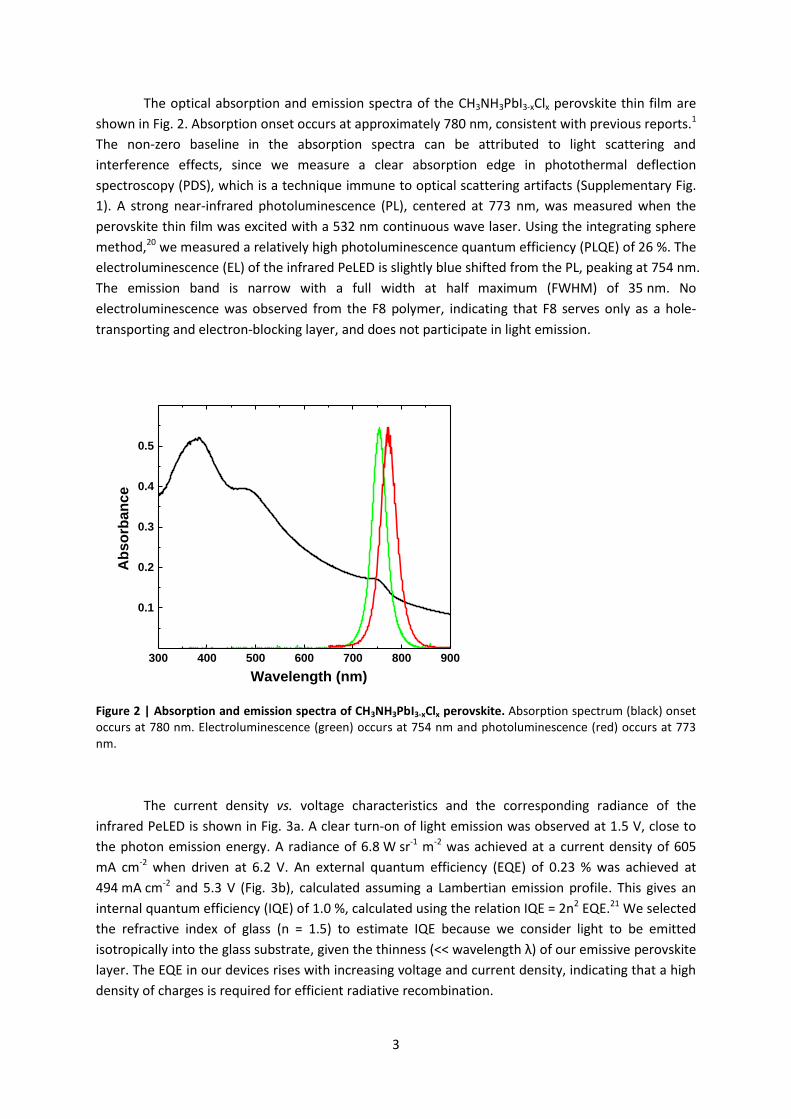
The optical absorption and emission spectra of the CH3NH3PbI3-xClx perovskite thin film are
shown in Fig. 2. Absorption onset occurs at approximately 780 nm, consistent with previous reports.1
The non-zero baseline in the absorption spectra can be attributed to light scattering and
interference effects, since we measure a clear absorption edge in photothermal deflection
spectroscopy (PDS), which is a technique immune to optical scattering artifacts (Supplementary Fig.
1). A strong near-infrared photoluminescence (PL), centered at 773 nm, was measured when the
perovskite thin film was excited with a 532 nm continuous wave laser. Using the integrating sphere
method,20 we measured a relatively high photoluminescence quantum efficiency (PLQE) of 26 %. The
electroluminescence (EL) of the infrared PeLED is slightly blue shifted from the PL, peaking at 754 nm.
The emission band is narrow with a full width at half maximum (FWHM) of 35 nm. No
electroluminescence was observed from the F8 polymer, indicating that F8 serves only as a hole-
transporting and electron-blocking layer, and does not participate in light emission.
Figure 2 | Absorption and emission spectra of CH3NH3PbI3-xClx perovskite. Absorption spectrum (black) onset occurs at 780 nm. Electroluminescence (green) occurs at 754 nm and photoluminescence (red) occurs at 773 nm.
The current density vs. voltage characteristics and the corresponding radiance of the
infrared PeLED is shown in Fig. 3a. A clear turn-on of light emission was observed at 1.5 V, close to
the photon emission energy. A radiance of 6.8 W sr-1 m-2 was achieved at a current density of 605
mA cm-2 when driven at 6.2 V. An external quantum efficiency (EQE) of 0.23 % was achieved at
494 mA cm-2 and 5.3 V (Fig. 3b), calculated assuming a Lambertian emission profile. This gives an
internal quantum efficiency (IQE) of 1.0 %, calculated using the relation IQE = 2n2 EQE.21 We selected
the refractive index of glass (n = 1.5) to estimate IQE because we consider light to be emitted
isotropically into the glass substrate, given the thinness (<< wavelength λ) of our emissive perovskite
layer. The EQE in our devices rises with increasing voltage and current density, indicating that a high
density of charges is required for efficient radiative recombination.
300 400 500 600 700 800 900
0.1
0.2
0.3
0.4
0.5
Ab
so
rban
ce
Wavelength (nm)

4
To investigate the reasons for the decline in radiance and efficiency at higher current
densities, we turned to pulse voltage measurements where a bias of 14 V was applied to drive
currents up to 1500 mA cm-2. Using square voltage pulses at a width of 1 ms and frequency of 100 Hz,
we achieved a two-times higher radiance of 13.1 W sr-1 m-2 at a current density of 1467 mA cm-2 (Fig.
3c). This indicates that the device degradation and efficiency drop-off are driven by heating at high
current densities since a higher radiance could be achieved when the device is given time to cool
between the pulses.
Interestingly, we observed during our pulse experiments that the radiance and quantum
efficiency of the PeLED increase across the duration of the voltage pulse, while the current density
remains approximately constant (Supplementary Fig. 2). We show, in Supplementary Fig. 3, that this
increase in light-emitting efficiency is related to the history of electric field polarization across the
device. In our experiments, a device which is pre-polarized with an external bias emits at a higher
radiance and efficiency. Over the duration of the voltage pulse, the perovskite device becomes
increasingly polarized, hence giving higher electroluminescence with longer pulse durations. This
polarization effect is also reflected in the hysteretic current-voltage characteristics of the PeLED, as
shown in Supplementary Fig. 4. A potential sweep from forward bias to reverse bias (i.e. larger
polarization history to smaller polarization) leads to higher radiance and EQE, compared to a sweep
from reverse to forward bias. We postulate that a high polarization voltage drives the ionic traps out
of the bulk emissive layer, therefore suppressing non-radiative trap-mediated recombination and
enhancing the radiative bimolecular recombination. A detailed discussion can be found in the
supplementary information.
In our experiments, we observe an increase in EL quantum efficiency with both increasing
voltage and current density (Fig. 3b and 3d). In order to investigate the relation of radiative
recombination with charge (or excitation) density, we measured photoluminescence quantum
efficiency (PLQE) as a function of laser excitation flux (Fig. 3d). We used a thin film structure of
TiO2/CH3NH3PbI3-xClx/F8 that is identical to our devices for measurement. The PLQE rises with laser
photon flux in a trend that is similar to the rise of device quantum efficiency with current density,
confirming that high charge densities are essential for efficient radiative recombination. In Fig. 3d,
we compare IQE vs. current density in the same plot as PLQE vs. absorbed photon flux, and find good
agreement between the quantum efficiencies obtained via laser excitation and electrical injection.
The extrapolation of IQE suggests that higher electroluminescence quantum efficiency may be
achievable at higher current densities. We note that the quantum efficiency of the pulsed device
also exhibits the same increase with current density, although efficiencies are lower compared to
the steady-state measurements due to the short pulse width of 1 ms (Supplementary Fig. 2). The
lower device EL quantum efficiencies compared to the PLQE suggest non-radiative losses by
electrical injection, which may be reduced by the optimization of device fabrication process if these
losses are predominantly due to high leakage currents.
We have previously demonstrated that radiative recombination in CH3NH3PbI3-xClx
perovskites is bimolecular in nature.10 The need for high excitation densities for efficient radiative
recombination suggests the presence of a competing non-radiative recombination pathway. Since
bimolecular recombination kinetics follow an n2 relationship (where n = excitation density), a
radiative bimolecular pathway can dominate at higher charge densities. With the fluxes produced in

5
our devices, charge densities are relatively low and the competing non-radiative channels dominate,
giving rise to a modest EL quantum efficiency.
It is interesting to note that a PLQE of 10 % can be achieved in a TiO2/CH3NH3PbI3-xClx/F8 film
structure. This is compared to a PLQE of 26 % for a pristine perovskite film of equivalent thickness at
an equivalent laser excitation flux. This confirms the formation of a charge confining well structure in
our devices, where excitations are only slightly quenched at the heterojunctions, despite an emissive
layer thickness of only 15 nm. To further demonstrate the effectiveness of our thin well structure,
we fabricated devices using thicker perovskite films (Supplementary Fig. 5). The radiance and
quantum efficiency of the devices decrease markedly at larger perovskite thicknesses,
demonstrating the need for spatial confinement of charges to ensure a high rate of electron-hole
capture and radiative recombination. In addition, reabsorption losses are likely to be lower in the
thinner films.
Figure 3 | Device characteristics of infrared PeLED. a, Combined radiance (black) and current density (red) vs. voltage characteristics of the infrared PeLED. The device turns on at 1.5 V. b, External quantum efficiency vs. voltage characteristics of PeLED. c, Radiance vs. current density of PeLED under steady state (black) and pulse
0 1 2 3 4 5 6
10-5
10-4
10-3
10-2
10-1
100
101
0 1 2 3 4 5 6
0.05
0.10
0.15
0.20
0.25
0 200 400 600 800 1000 1200 14000
2
4
6
8
10
12
14
5.0x10¹⁸
1.0x10¹⁹
1.5x10¹⁹
0
2
4
6
8
10
0
2
4
6
8
10
Rad
ian
ce
(W
sr-1
m-2)
Voltage (V)
10-3
10-2
10-1
100
101
102
103
104
Cu
rre
nt
Den
sit
y (
mA
cm
-2)
Ex
tern
al
Qu
an
tum
Eff
icie
nc
y (
%)
Voltage (V)
Rad
ian
ce
(W
sr-1
m-2)
Current Density (mA cm-2)
IQ
E (
%)
PL
QE
(%
)
Photon or charge flux (s-1 cm
-2)
a b
c d0 500 1000 1500 2000
Current Density (mA cm-2)

6
measurement (red) conditions. For pulse measurement, 1 ms square voltage pulses were applied at a frequency of 100 Hz. d, Photoluminescence quantum efficiency (PLQE) (black) of TiO2/CH3NH3PbI3-xClx/F8 layers as a function of absorbed (~15%) photon flux. Device Internal quantum efficiency (IQE) in steady-state measurement (red) and in pulse measurement (grey) are plotted against current density on the same graph for comparison. Dotted lines represent extrapolation of quantum efficiencies towards higher current density.
Our findings suggest that higher charge densities, higher polarization and thinner emission
layers are possible routes towards enhancing the electroluminescence efficiency. However, we note
that the surface coverage of the CH3NH3PbI3-xClx perovskite is incomplete (~30 % voids) in such thin
layers (Supplementary Fig. 6), causing possible contact between the TiO2 and F8 layers. In order to
investigate the effects of electrical shunts at TiO2/F8 interfaces, we fabricated a TiO2/F8 device
without the thin perovskite layer. We find the current density of the TiO2/F8 device to be several
times higher than the perovskite device at forward bias (Supplementary Fig. 7), indicating that there
are possible current losses at the TiO2/F8 interface that do not contribute to electroluminescence.
Optimization of thin film formation and morphology towards complete perovskite coverage is
therefore expected to enhance device radiance and quantum efficiency. We further note that the EL
photon flux from the F8-only device is 3 orders of magnitude lower than the perovskite device,
confirming that the F8 layer does not participate in light emission but serves only as a hole-
transporting and electron-blocking layer.
In an effort to optimize our device efficiencies and to minimize luminescence quenching at
the TiO2/perovskite interface, we inserted an ultra-thin (1 nm) layer of Al2O3 in between the TiO2 and
the perovskite layers using atomic layer deposition. With this minor modification, we achieved a
two-fold enhanced radiance of 13.2 W sr-1 m-2 at a lower current density of 363 mA cm-2 (Fig. 4a).
Consequently, the device EQE and IQE increased by more than 3 times to 0.76 % and 3.4 %
respectively (Fig. 4b). This level of performance is comparable or better than some of the best
colloidal quantum dot infrared light-emitting devices.22,23 This enhancement in luminescent
efficiency is likely due to the surface-induced nano-structuring of the perovskite layer24 and the
suppression of luminescence quenching at the TiO2/perovskite interface.

7
Figure 4 | Device characteristics of infrared PeLED modified with Al2O3. a, Combined radiance (black) and current density (red) vs. voltage characteristics of a modified ITO/TiO2/Al2O3(1nm)/CH3NH3PbI3-
xClx/F8/MoO3/Ag infrared PeLED. b, External quantum efficiency vs. voltage characteristics of modified infrared PeLED.
In order to demonstrate the application of organometal halide perovskite as visible light
emitters, we utilized the larger bandgap CH3NH3PbBr3 as a green emitter in our PeLED devices. Since
a larger bandgap makes it more challenging to achieve electron injection from TiO2 into the
perovskite conduction band, we turned to an inverted device structure with an
ITO/PEDOT:PSS/CH3NH3PbBr3/F8/Ca/Ag architecture. PEDOT:PSS and calcium were utilized as ohmic
hole and electron injectors respectively. The F8 polymer (50 nm) serves as a spacer layer for electron
transport and to prevent emission quenching near the Ca metal interface. In order to spatially
confine injected charges for efficient radiative recombination, we fabricated CH3NH3PbBr3 to a
thickness of 20 nm (film morphology shown in Supplementary Fig. 8). As shown in Fig. 5a, bright
green electroluminescence was achieved at 517 nm. The PL of CH3NH3PbBr3 perovskite is slightly
red-shifted from the EL, peaking at 524 nm with a PLQE of 7 % when excited with a 405 nm laser.
The device turns on at 3.3 V and reaches a luminance of 364 cd m-2 at a current density of 123 mA
cm-2, as shown in Fig. 5b. This gives an efficiency of 0.3 cd A-1, or an EQE of 0.1 % and an IQE of 0.4 %
(Fig. 5c), assuming a Lambertian emission profile. Similar to the infrared device, the EL quantum
efficiency increases with injection current density (Fig. 5d), demonstrating a need for high charge
densities to achieve efficient radiative recombination. We also demonstrate red
electroluminescence at 630 nm using a CH3NH3PbBr2I mixed halide perovskite in the same device
architecture (device characteristics in Supplementary Fig. 9), showing the versatility and wide
bandgap tunability of these organometal halide perovskites.
0 1 2 3 4 5 6 7 8
10-5
10-4
10-3
10-2
10-1
100
101
0 1 2 3 4 5 6 7 8
0.1
0.2
0.3
0.4
0.5
0.6
0.7
0.8
Rad
ian
ce
(W
sr-1
m-2)
Voltage (V)
10-3
10-2
10-1
100
101
102
103
104
Cu
rre
nt
Den
sit
y (
mA
cm
-2)
Ex
tern
al
Qu
an
tum
Eff
icie
nc
y (
%)
Voltage (V)
a b

8
Figure 5 | Device characteristics of visible PeLED. a, Absorption (black), electroluminescence (green, solid) and photoluminescence (green, dashed) spectra of CH3NH3PbBr3 perovskite. Electroluminescence of CH3NH3PbBr2I mixed halide perovskite shown in red. Inset image shows uniform green and red electroluminescence from ITO/PEDOT:PSS/CH3NH3PbBr3/F8/Ca/Ag and ITO/PEDOT:PSS/CH3NH3PbBr2I/F8/Ca/Ag PeLED respectively. b, Combined luminance (black) and current density (red) vs. voltage characteristics of green PeLED. The device turns on at 3.3 V. c, External quantum efficiency vs. voltage characteristics of green PeLED. d, External quantum efficiency vs. current density of green PeLED. Inset diagram shows green PeLED device structure.
Our demonstration of bright visible and infrared electroluminescence from organometal
halide based perovskites shows great promise in the development of this class of materials for large
area optoelectronics or electrically-pumped lasing applications.10,25 Furthermore, our work
exemplifies the fact that an efficient solar cell material is generally also a good light emitter, as given
by the Shockley-Queisser detailed balance limit calculations.26,27 It is interesting that bright
electroluminescence could be achieved using a simple thin emitter realized by solution processing.
Given the versatility and low-cost processability of these organometal halide perovskites, they may
quickly find their way into the display and lighting industry.
400 500 600 700 800 9000.00
0.05
0.10
0.15
0.20
0 1 2 3 4 5 6 7 8
0.01
0.1
1
10
100
0 1 2 3 4 5 6 7 80.00
0.02
0.04
0.06
0.08
0.10
0 20 40 60 80 100 1200.00
0.02
0.04
0.06
0.08
0.10
Ab
so
rba
nc
e
Wavelength (nm)
Lu
min
an
ce
(c
d m
-2)
Voltage (V)
1
10
100
Cu
rre
nt
Den
sit
y (
mA
cm
-2)
Ex
tern
al
Qu
an
tum
Eff
icie
nc
y (
%)
Voltage (V)
a b
c d
0.0
0.1
0.2
0.3
Eff
icie
nc
y (
cd
A-1)
Ex
tern
al
Qu
an
tum
Eff
icie
nc
y (
%)
Current Density (mA cm-2)

9
Materials and Methods
F8 polymer was provided by Cambridge Display Technology (CDT) and was used as received. All
other chemicals were purchased from Sigma-Aldrich and were used as received.
CH3NH3PbI3-xClx Perovskite Synthesis. Methylammonium iodide (CH3NH3I) was prepared by adding 33
wt % methylamine solution in ethanol (24 mL) and 57 wt % hydroiodic acid in water (10 mL) to 100
mL of absolute ethanol. The reaction mixture was stirred at room temperature in a nitrogen
atmosphere. The solvent was removed by rotary evaporation until white crystals started to appear.
The product was collected using Büchner funnel filtration and was dried overnight under vacuum at
80 °C. The mixed halide perovskite precursor solution was prepared by mixing CH3NH3I and PbCl2 in a
3:1 molar ratio in anhydrous N,N-dimethylformamide to give a concentration of 5 wt %.
CH3NH3PbBr3 Perovskite Synthesis. Methylammonium bromide (CH3NH3Br) was prepared by adding
33 wt % methylamine solution in ethanol (24 mL) and 48 wt % hydrobromic acid in water (8.5 mL) to
100 mL of absolute ethanol. The reaction mixture was stirred at room temperature. The solvent was
removed by rotary evaporation. The obtained white crystals were washed with anhydrous diethyl
ether and recrystallized in ethanol. The perovskite precursor solution was prepared by mixing
CH3NH3Br and PbBr2 in a 3:1 molar ratio in anhydrous N,N-dimethylformamide to give a
concentration of 5 wt %. For the CH3NH3PbBr2I mixed-halide precursor solution, we mixed the
individual CH3NH3PbBr3 and CH3NH3PbI3 precursor solutions in a molar ratio of 2:1 to give an overall
concentration of 5 wt %.
Infrared PeLED Fabrication. ITO-coated glass substrates were cleaned successively with acetone and
isopropanol. TiO2 (25 nm) was grown onto the cleaned substrates at 225 °C with atomic layer
deposition (ALD), using titanium tetrachloride (TiCl4) and water as precursors. The substrates were
transferred into a nitrogen filled glovebox for further fabrication. The CH3NH3PbI3-xClx perovskite
precursor solution was spin-coated onto the TiO2 at 3000 rpm for 60 seconds, and annealed at
100 °C for 5 minutes to give a thin perovskite film with an average thickness of ~15 nm, as
determined by atomic force microscopy (AFM). A solution of F8 in chlorobenzene (10 mg/mL) was
spin-coated onto the perovskite layer at 3000 rpm for 60 seconds to give a 50 nm film. MoO3 (5 nm)
and Ag (100 nm) were successively deposited by vacuum thermal evaporation. Devices were tested
in air without encapsulation.
Green PeLED Fabrication. ITO-coated glass substrates were cleaned successively with acetone and
isopropanol, followed by 10 minutes oxygen plasma treatment. PEDOT:PSS (Clevios P VP AI 4083)
was spin-coated onto the substrate at 6000 rpm for 30 seconds, and annealed at 140 °C for 30
minutes in a nitrogen atmosphere. The CH3NH3PbBr3 perovskite precursor solution was spin-coated
onto PEDOT:PSS at 3000 rpm for 30 seconds and annealed at 100 °C for 15 minutes to give a
perovskite film thickness of ~20 nm. A solution of F8 in chlorobenzene (10 mg/mL) was spin-coated
onto the perovskite layer at 3000 rpm for 30 seconds to give a 50 nm film. Ca (20 nm) and Ag (100
nm) were successively deposited by vacuum thermal evaporation. Devices were tested in air without
encapsulation.
PeLED Characterization. Current vs. voltage characteristics were measured using a Keithley 2400
Source Measure Unit (SMU). Photon flux was measured simultaneously using a calibrated silicon
photodiode centered over the light-emitting pixel. Radiance in W sr-1 m-2 and luminance in cd m-2

10
were calculated based on the emission function of the PeLED, and on the known spectral response
of the silicon photodiode. External quantum efficiency was calculated, assuming a Lambertian
emission profile. Electroluminescence spectra were measured using a Labsphere CDS-610
spectrometer.
PLQE Measurement. The PLQE of the thin film samples was measured using an integrating sphere
method, as reported in the literature.20 A continuous wave 532 nm green diode laser with an
excitation power of 10 – 100 mW and a focused beam spot of ~0.3 mm2 was used to photo-excite
the samples. Emission was measured using an Andor iDus DU490A InGaAs detector. During
measurements, the samples were kept at room temperature under a constant stream of nitrogen.
Samples were prepared in the structure TiO2/CH3NH3PbI3-xClx/F8 on top of a spectrosil fused silica
substrate, similar to the PeLED device structure.
Pulse LED Measurement. A square voltage pulse with a pulse width of 1 ms and frequency of 100 Hz
was applied to the device using a HP8116A Pulse/Function generator. A dual-channel Agilent
Technologies DSO6032A oscilloscope, set to 50 Ω impedance, was connected in series to the device
and the function generator to determine the current through the device. The electroluminescence
was monitored using a calibrated Si photodiode, connected to the 2nd channel of the oscilloscope (1
MΩ) via a Thorlabs PDA200C photodiode amplifier.

11
References
1 Lee, M. M., Teuscher, J., Miyasaka, T., Murakami, T. N. & Snaith, H. J. Efficient Hybrid Solar Cells Based on Meso-Superstructured Organometal Halide Perovskites. Science 338, 643-647 (2012).
2 Kim, H.-S. et al. Lead Iodide Perovskite Sensitized All-Solid-State Submicron Thin Film Mesoscopic Solar Cell with Efficiency Exceeding 9%. Sci. Rep. 2 (2012).
3 Burschka, J. et al. Sequential deposition as a route to high-performance perovskite-sensitized solar cells. Nature 499, 316-319 (2013).
4 Liu, M., Johnston, M. B. & Snaith, H. J. Efficient planar heterojunction perovskite solar cells by vapour deposition. Nature 501, 395-398 (2013).
5 Stranks, S. D. et al. Electron-Hole Diffusion Lengths Exceeding 1 Micrometer in an Organometal Trihalide Perovskite Absorber. Science 342, 341-344 (2013).
6 Xing, G. et al. Long-Range Balanced Electron- and Hole-Transport Lengths in Organic-Inorganic CH3NH3PbI3. Science 342, 344-347 (2013).
7 Heo, J. H. et al. Efficient inorganic-organic hybrid heterojunction solar cells containing perovskite compound and polymeric hole conductors. Nat Photon 7, 486-491 (2013).
8 Stoumpos, C. C., Malliakas, C. D. & Kanatzidis, M. G. Semiconducting Tin and Lead Iodide Perovskites with Organic Cations: Phase Transitions, High Mobilities, and Near-Infrared Photoluminescent Properties. Inorganic Chemistry 52, 9019-9038 (2013).
9 Noh, J. H., Im, S. H., Heo, J. H., Mandal, T. N. & Seok, S. I. Chemical Management for Colorful, Efficient, and Stable Inorganic–Organic Hybrid Nanostructured Solar Cells. Nano Letters 13, 1764-1769 (2013).
10 Deschler, F. et al. High Photoluminescence Efficiency and Optically Pumped Lasing in Solution-Processed Mixed Halide Perovskite Semiconductors. The Journal of Physical Chemistry Letters 5, 1421-1426 (2014).
11 Schmidt, L. C. et al. Nontemplate Synthesis of CH3NH3PbBr3 Perovskite Nanoparticles. Journal of the American Chemical Society 136, 850-853 (2014).
12 Era, M., Morimoto, S., Tsutsui, T. & Saito, S. Organic‐inorganic heterostructure electroluminescent device using a layered perovskite semiconductor (C6H5C2H4NH3)2PbI4. Applied Physics Letters 65, 676-678 (1994).
13 Hattori, T., Taira, T., Era, M., Tsutsui, T. & Saito, S. Highly efficient electroluminescence from a heterostructure device combined with emissive layered-perovskite and an electron-transporting organic compound. Chemical Physics Letters 254, 103-108 (1996).
14 Chondroudis, K. & Mitzi, D. B. Electroluminescence from an Organic−Inorganic Perovskite Incorporating a Quaterthiophene Dye within Lead Halide Perovskite Layers. Chemistry of Materials 11, 3028-3030 (1999).
15 Tanaka, K. et al. Comparative study on the excitons in lead-halide-based perovskite-type crystals CH3NH3PbBr3 CH3NH3PbI3. Solid State Communications 127, 619-623 (2003).
16 Hirasawa, M., Ishihara, T., Goto, T., Uchida, K. & Miura, N. Magnetoabsorption of the lowest exciton in perovskite-type compound (CH3NH3)PbI3. Physica B: Condensed Matter 201, 427-430 (1994).
17 Lu, L.-P., Kabra, D., Johnson, K. & Friend, R. H. Charge-Carrier Balance and Color Purity in Polyfluorene Polymer Blends for Blue Light-Emitting Diodes. Advanced Functional Materials 22, 144-150 (2012).
18 Abrusci, A. et al. High-Performance Perovskite-Polymer Hybrid Solar Cells via Electronic Coupling with Fullerene Monolayers. Nano Letters 13, 3124-3128 (2013).
19 Hwang, J. et al. Photoelectron Spectroscopic Study of the Electronic Band Structure of Polyfluorene and Fluorene-Arylamine Copolymers at Interfaces. The Journal of Physical Chemistry C 111, 1378-1384 (2006).

12
20 de Mello, J. C., Wittmann, H. F. & Friend, R. H. An improved experimental determination of external photoluminescence quantum efficiency. Advanced Materials 9, 230-232 (1997).
21 Greenham, N. C., Friend, R. H. & Bradley, D. D. C. Angular Dependence of the Emission from a Conjugated Polymer Light-Emitting Diode: Implications for efficiency calculations. Advanced Materials 6, 491-494 (1994).
22 Tessler, N., Medvedev, V., Kazes, M., Kan, S. & Banin, U. Efficient Near-Infrared Polymer Nanocrystal Light-Emitting Diodes. Science 295, 1506-1508 (2002).
23 Sun, L. et al. Bright infrared quantum-dot light-emitting diodes through inter-dot spacing control. Nat Nano 7, 369-373 (2012).
24 Choi, J. J., Yang, X., Norman, Z. M., Billinge, S. J. L. & Owen, J. S. Structure of Methylammonium Lead Iodide Within Mesoporous Titanium Dioxide: Active Material in High-Performance Perovskite Solar Cells. Nano Letters 14, 127-133 (2013).
25 Xing, G. et al. Low-temperature solution-processed wavelength-tunable perovskites for lasing. Nat Mater 13, 476-480 (2014).
26 Shockley, W. & Queisser, H. J. Detailed Balance Limit of Efficiency of p‐n Junction Solar Cells. Journal of Applied Physics 32, 510-519 (1961).
27 Miller, O. D., Yablonovitch, E. & Kurtz, S. R. Strong Internal and External Luminescence as Solar Cells Approach the Shockley-Queisser Limit. Photovoltaics, IEEE Journal of 2, 303-311 (2012).
Acknowledgements
We thank EPSRC (UK) for financial support. Z.K.T. thanks the Singapore National Research
Foundation (Energy Innovation Program Office) for the research scholarship. T.B. thanks the LMU
Center of NanoScience, the Excellence Cluster Nanosystems Initiative Munich (NIM) and the
Bavarian Network “Solar Technologies Go Hybrid" for financial support.
Author contributions
Original device architectures conceived by Z.K.T. Z.K.T. designed and fabricated the PeLED,
performed most experiments and data analyses, and wrote the paper. R.S.M. optimized the
electron-injection layers in devices. M.L.L. fabricated the red PeLED. P.D., R.H. and F.H. prepared the
perovskite materials. R.H., F.D. and M.P. assisted with PLQE studies. A.S. performed PDS studies.
L.M.P. and D.C. assisted with experiments. T.B. and H.J.S. provided important insights. R.H.F. guided
the work.
Additional information
Supplementary information accompanies this paper at
www.nature.com/naturenanotechnology. Reprints and permission information is
available online at http://npg.nature.com/reprintsandpermissions/. Correspondence and requests
for materials should be addressed to R.H.F.