bq24620 stand-alone synchronous switched-mode · pdf filewith low iq 1 features 2 applications...
TRANSCRIPT

bq24
620 Battery
pack
HIDRV
LODRV
PH
SRNSRP
VFB
CE
VREF
ISET
ADAPTER
ADAPTERSTAT
PG
VREF
TS
Product
Folder
Sample &Buy
Technical
Documents
Tools &
Software
Support &Community
bq24620SLUS893B –MARCH 2010–REVISED JUNE 2015
bq24620 Stand-Alone Synchronous Switched-Mode Lithium Phosphate Battery ChargerWith Low Iq
1 Features 2 Applications1• 300-kHz NMOS-NMOS Synchronous Buck • Power Tools and Portable Equipment
Converter • Personal Digital Assistants• Stand-Alone Charger Designed Specifically for • Handheld Terminals
Lithium Phosphate • Industrial and Medical Equipment• 5-V to 28-V VCC Operating Range, Supports 1 to • Netbooks, Mobile Internet Devices, and
7 Battery Cells Ultramobile PCs• High-Accuracy Voltage and Current Regulation
3 Description– ±0.5% Charge Voltage AccuracyThe bq24620 device is a highly integrated lithium– ±3% Charge Current Accuracyphosphate switched-mode battery charge controller.• Integration The device offers a constant-frequency synchronous
– Internal Loop Compensation switching PWM controller with high-accuracy chargecurrent and voltage regulation, charge– Internal Soft Startpreconditioning, termination, and charge status• Safetymonitoring.
– Input Overvoltage ProtectionThe bq24620 charges the battery in three phases:– Battery Thermistor Sense Suspend Charge at preconditioning, constant current, and constantHot/Cold Charge Suspend and Automatically voltage.ICHARGE/8 at WARM/COOL
– Battery Detection Device Information(1)
PART NUMBER PACKAGE BODY SIZE (NOM)– Built-In Safety Timerbq24620 VQFN (16) 3.50 mm × 3.50 mm– Charge Overcurrent Protection(1) For all available packages, see the orderable addendum at– Battery Short Protection
the end of the data sheet.– Battery Overvoltage Protection– Thermal Shutdown Simplified Schematic
• Status Outputs– Adapter Present– Charger Operation Status
• Charge Enable Pin• 6-V Gate Drive for Synchronous Buck Converter• 30-ns Driver Dead Time and 99.95% Maximum
Effective Duty Cycle• 16-Pin 3.5-mm × 3.5-mm QFN Package• Energy Star Low Iq
– < 15-μA Off-State Battery Discharge Current– < 1.5-mA Off-State Input Quiescent Current
1
An IMPORTANT NOTICE at the end of this data sheet addresses availability, warranty, changes, use in safety-critical applications,intellectual property matters and other important disclaimers. PRODUCTION DATA.

bq24620SLUS893B –MARCH 2010–REVISED JUNE 2015 www.ti.com
Table of Contents8.4 Device Functional Modes........................................ 221 Features .................................................................. 1
9 Application and Implementation ........................ 232 Applications ........................................................... 19.1 Application Information............................................ 233 Description ............................................................. 19.2 Typical Application ................................................. 234 Revision History..................................................... 2
10 Power Supply Recommendations ..................... 295 Device Comparison Table ..................................... 311 Layout................................................................... 296 Pin Configuration and Functions ......................... 3
11.1 Layout Guidelines ................................................. 297 Specifications......................................................... 411.2 Layout Example .................................................... 307.1 Absolute Maximum Ratings ..................................... 4
12 Device and Documentation Support ................. 317.2 ESD Ratings.............................................................. 512.1 Device Support...................................................... 317.3 Recommended Operating Conditions....................... 512.2 Documentation Support ........................................ 317.4 Thermal Information .................................................. 512.3 Community Resources.......................................... 317.5 Electrical Characteristics........................................... 512.4 Trademarks ........................................................... 317.6 Typical Characteristics .............................................. 912.5 Electrostatic Discharge Caution............................ 318 Detailed Description ............................................ 1112.6 Glossary ................................................................ 318.1 Overview ................................................................. 11
13 Mechanical, Packaging, and Orderable8.2 Functional Block Diagram ....................................... 12Information ........................................................... 318.3 Feature Description................................................. 13
4 Revision History
Changes from Revision A (October 2011) to Revision B Page
• Added ESD Ratings table, Feature Description section, Device Functional Modes, Application and Implementationsection, Power Supply Recommendations section, Layout section, Device and Documentation Support section, andMechanical, Packaging, and Orderable Information section .................................................................................................. 1
Changes from Original (March 2010) to Revision A Page
• Changed description for PH and BTST pins .......................................................................................................................... 4• Replaced Thermal Information table ...................................................................................................................................... 5• Corrected Equation 11 ......................................................................................................................................................... 24
2 Submit Documentation Feedback Copyright © 2010–2015, Texas Instruments Incorporated
Product Folder Links: bq24620

16 15 14 13
5 6 7 8
12
11
10
9
1
2
3
4
VCC
CE
STAT
TS
ISE
T
VR
EF
VF
B
SRN
SRP
GND
LO
DR
V
REGN
PH
HID
RV
BT
ST
OAR(bq24620)
QFN-16TOP VIEW
PG
bq24620www.ti.com SLUS893B –MARCH 2010–REVISED JUNE 2015
5 Device Comparison Table
bq24620 bq24630Cell chemistry Lithium phosphate Lithium phosphateNumber of cells in series (minimum to 1 to 7 1 to 7maximum, 4.2 V/cell)Charge voltage (minimum to maximum) (V) 1.8 to 26 1.8 to 26Input voltage range (minimum to maximum) (V) 5 to 28 5 to 28Input overvoltage (V) 32 32Maximum battery charging current (A) 10 10Switching frequency (kHz) 300 300JEITA charging temperature profile No NoDPM No IIN DPM
6 Pin Configuration and Functions
RVA Package16-Pin VQFN
Top View
Pin FunctionsPIN
DESCRIPTIONNAME NO.BTST 16 PWM high-side driver negative supply. Connect the 0.1-μF bootstrap capacitor from PH to BTST, and a bootstrap
Schottky diode from REGN to BTST.CE 2 Charge enable active-HIGH logic input. HI enables charge. LO disables charge. The CE pin has an internal 1-MΩ
pulldown resistor.GND 11 Low-current sensitive analog/digital ground. On PCB layout, connect with thermal pad underneath the IC.HIDRV 15 PWM high-side driver output. Connect to the gate of the high-side power MOSFET with a short trace.ISET 7 Charge current set input. The voltage of ISET pin programs the charge current regulation, precharge current and
termination current set-point.LODRV 13 PWM low-side driver output. Connect to the gate of the low-side power MOSFET with a short trace.
Copyright © 2010–2015, Texas Instruments Incorporated Submit Documentation Feedback 3
Product Folder Links: bq24620
bq24620SLUS893B –MARCH 2010–REVISED JUNE 2015 www.ti.com
Pin Functions (continued)PIN
DESCRIPTIONNAME NO.PG 5 Open-drain power good status output. The transistor turns on when a valid VCC is detected. The transistor is turned
off in the sleep mode. PG can be used to drive an LED or communicate with a host processor. The PG pin can beused to drive ACFET and BATFET.
PH 14 PWM high-side driver negative supply. Connect to the phase-switching node (junction of the low-side power MOSFETdrain, high-side power MOSFET source, and output inductor).
REGN 12 PWM low-side driver positive 6-V supply output. Connect a 1-μF ceramic capacitor from REGN to the PGND pin, closeto the IC. Use for low-side driver and high-side driver bootstrap voltage by connecting a small-signal Schottky diodefrom REGN to BTST.
SRN 9 Charge current sense resistor, negative input. A 0.1-μF ceramic capacitor is placed from SRN to SRP to providedifferential-mode filtering. An optional 0.1-μF ceramic capacitor is placed from the SRN pin to GND for common-modefiltering.
SRP 10 Charge current sense resistor, positive input. A 0.1-μF ceramic capacitor is placed from SRN to SRP to providedifferential-mode filtering. A 0.1-μF ceramic capacitor is placed from SRP pin to GND for common-mode filtering.
STAT 3 Open-drain charge status pin to indicate various charger operations (See Table 2)Thermal — Exposed pad beneath the IC. Always solder the thermal pad to the board, and have vias on the thermal-pad planepad star-connecting to GND and ground plane for high-current power converter. It also serves as a thermal pad to
dissipate the heat.TS 4 Temperature qualification voltage input for battery pack negative-temperature-coefficient thermistor. Program the hot
and cold temperature window with a resistor divider from VREF to TS to GND.VCC 1 IC power positive supply. Connect through a 10-Ω resistor to the common-source (diode-OR) point: source of high-
side P-channel MOSFET and source of reverse-blocking power P-channel MOSFET. Or connect through a 10-Ωresistor to the cathode of the input diode. Place a 1-μF ceramic capacitor from VCC to GND pin close to the IC.
VFB 8 Output voltage analog feedback adjustment. Connect the output of a resistive voltage divider from the batteryterminals to this node to adjust the output battery regulation voltage.
VREF 6 3.3-V regulated voltage output. Place a 1-μF ceramic capacitor from VREF to the GND pin close to the IC. Thisvoltage could be used for programming of voltage and current regulation and for programming the TS threshold.
7 Specifications
7.1 Absolute Maximum Ratings (1) (2) (3)
over operating free-air temperature range (unless otherwise noted)MIN MAX UNIT
VCC, SRP, SRN, CE, STAT, PG –0.3 33PH –2 36VFB –0.3 16
Voltage VREGN, LODRV, TS –0.3 7BTST, HIDRV with respect to GND –0.3 39VREF, ISET –0.3 3.6
Maximum difference voltage SRP–SRN –0.5 0.5 VJunction temperature, TJ –40 155 °CStorage temperature, Tstg –55 155 °C
(1) Stresses beyond those listed under Absolute Maximum Ratings may cause permanent damage to the device. These are stress ratingsonly, and functional operation of the device at these or any other conditions beyond those indicated under Recommended OperatingConditions is not implied. Exposure to absolute-maximum-rated conditions for extended periods may affect device reliability.
(2) All voltages are with respect to GND if not specified. Currents are positive into, negative out of the specified terminal. Consult thepackaging section of the data book for thermal limitations and considerations of packages.
(3) Must have a series resistor between battery pack to VFB if battery pack voltage is expected to be greater than 16 V. Usually theresistor-divider top resistor takes care of this.
4 Submit Documentation Feedback Copyright © 2010–2015, Texas Instruments Incorporated
Product Folder Links: bq24620
bq24620www.ti.com SLUS893B –MARCH 2010–REVISED JUNE 2015
7.2 ESD RatingsVALUE UNIT
Human body model (HBM), per ANSI/ESDA/JEDEC JS-001 (1) ±2000V(ESD) Electrostatic discharge VCharged device model (CDM), per JEDEC specification JESD22- ±500
C101 (2)
(1) JEDEC document JEP155 states that 500-V HBM allows safe manufacturing with a standard ESD control process.(2) JEDEC document JEP157 states that 250-V CDM allows safe manufacturing with a standard ESD control process.
7.3 Recommended Operating ConditionsMIN NOM MAX UNIT
VCC, SRP, SRN, CE, STAT, PG –0.3 28PH –2 30VFB –0.3 14
Voltage REGN, LODRV, TS –0.3 6.5 VBTST, HIDRV with respect to GND –0.3 34ISET –0.3 3.3VREF 3.3
Maximum difference SRP–SRN –0.2 0.2 VvoltageTJ Junction temperature 0 125 °CTstg Storage temperature –55 155 °C
7.4 Thermal Informationbq24620
THERMAL METRIC (1) RVA [VQFN] UNIT16 PINS
RθJA Junction-to-ambient thermal resistance 43.8 °C/WRθJC(top) Junction-to-case (top) thermal resistance 81 °C/WRθJB Junction-to-board thermal resistance 16 °C/WψJT Junction-to-top characterization parameter 0.6 °C/WψJB Junction-to-board characterization parameter 15.77 °C/WRθJC(bot) Junction-to-case (bottom) thermal resistance 4 °C/W
(1) For more information about traditional and new thermal metrics, see the Semiconductor and IC Package Thermal Metrics applicationreport, SPRA953.
7.5 Electrical Characteristics5 V ≤ VVCC ≤ 28 V, 0°C < TJ< 125°C, typical values are at TA= 25°C, with respect to GND unless otherwise noted
PARAMETER TEST CONDITIONS MIN TYP MAX UNIT
OPERATING CONDITIONS
VVCC_OP VCC input voltage operating range 5 28 V
QUIESCENT CURRENTS
Total battery discharge current (sum ofIBAT currents into VCC, BTST, PH, SRP, VVCC < VSRN, VVCC > VUVLO (SLEEP) 15 μA
SRN, VFB), VFB ≤ 2.1 V
VVCC > VSRN, VVCC > VUVLO CE = LOW (IC quiescent 1 1.5current)
Adapter supply current (current into VVCC > VSRN, VVCC >VVCCLOW , CE = HIGH, chargeIAC 2 5 mAVCC pin) done
VVCC > VSRN, VVCC >VVCCLOW , CE = HIGH, 12Charging, Qg_total = 20 nC, VVCC = 20 V
CHARGE VOLTAGE REGULATION
VFB Feedback regulation voltage 1.8 V
Copyright © 2010–2015, Texas Instruments Incorporated Submit Documentation Feedback 5
Product Folder Links: bq24620

bq24620SLUS893B –MARCH 2010–REVISED JUNE 2015 www.ti.com
Electrical Characteristics (continued)5 V ≤ VVCC ≤ 28 V, 0°C < TJ< 125°C, typical values are at TA= 25°C, with respect to GND unless otherwise noted
PARAMETER TEST CONDITIONS MIN TYP MAX UNIT
TJ = 0°C to 85°C –0.5% 0.5%Charge voltage regulation accuracy
TJ = –40°C to 125°C –0.7% 0.7%
IVFB Input leakage current into VFB pin VFB = 1.8 V 100 nA
CURRENT REGULATION – FAST CHARGE
VISET ISET voltage range 0 2 V
VIREG_CHG SRP–SRN current-sense voltage range VIREG_CHG = VSRP – VSRN 0 100 mV
Charger current-set factor; amps ofKISET RSENSE = 10 mΩ 5 A/Vcharge current per volt on ISET pin)
VIREG_CHG = 40 mV –3% 3%
VIREG_CHG = 20 mV –4% 4%Charge current regulation accuracy
VIREG_CHG = 5 mV –25% 25%
VIREG_CHG = 1.5 mV (VSRN > 3.1 V) –40% 40%
IISET Leakage current in to ISET Pin VISET = 2 V 100 nA
CURRENT REGULATION – PRECHARGE
Precharge current RSENSE = 10 mΩ, VFB < VLOWV 50 125 200 mA
CHARGE TERMINATION
Termination current range RSENSE = 10 mΩ ICHARGE/10 A
Termination current-set factor; amps ofKTERM 0.5 A/Vtermination current per volt on ISET pin
VITERM = 10 mV –10% 10%
Termination current accuracy VITERM = 5 mV –25% 25%
VITERM = 1.5 mV –45% 45%
Deglitch time for termination (both 100 msedge)
tQUAL Termination qualification time VBAT > VRECH and ICHARGE < ITERM 250 ms
IQUAL Termination qualification time Discharge current once termination is detected 2 mA
INPUT UNDERVOLTAGE LOCKOUT COMPARATOR (UVLO)
VUVLO AC undervoltage rising threshold Measure on VCC 3.65 3.85 4 V
VUVLO_HYS AC undervoltage hysteresis, falling 350 mV
VCC LOWV COMPARATOR
Falling threshold, disable charge Measure on VCC 4.1 V
Rising threshold, resume charge 4.35 4.5 V
SLEEP COMPARATOR (REVERSE DISCHARGING PROTECTION)
VSLEEP _FALL SLEEP falling threshold VVCC – VSRN to enter SLEEP 40 100 150 mV
VSLEEP_HYS SLEEP hysteresis 500 mV
SLEEP rising delay VCC falling below SRN, delay to pull up PG 1 µs
SLEEP falling delay VCC rising above SRN, delay to pull down PG 30 ms
SLEEP rising shutdown deglitch VCC falling below SRN, Delay to enter SLEEP mode 100 ms
VCC rising above SRN, Delay to come out of SLEEPSLEEP falling powerup deglitch 30 msmode
BAT LOWV COMPARATOR
LOWV rising threshold (precharge toVLOWV Measured on VFB pin 0.333 0.35 0.367 Vfast charge)
VLOWV_HYS LOWV hysteresis 100 mV
LOWV rising deglitch VFB falling below VLOWV 25 ms
LOWV falling deglitch VFB rising above VLOWV + VLOWV_HYS 25 ms
RECHARGE COMPARATOR
Recharge threshold (with respect toVRECHG Measured on VFB pin 110 125 140 mVVREG)
Recharge rising deglitch VFB decreasing below VRECHG 10 ms
Recharge falling deglitch VFB increasing above VRECHG 10 ms
6 Submit Documentation Feedback Copyright © 2010–2015, Texas Instruments Incorporated
Product Folder Links: bq24620

bq24620www.ti.com SLUS893B –MARCH 2010–REVISED JUNE 2015
Electrical Characteristics (continued)5 V ≤ VVCC ≤ 28 V, 0°C < TJ< 125°C, typical values are at TA= 25°C, with respect to GND unless otherwise noted
PARAMETER TEST CONDITIONS MIN TYP MAX UNIT
BAT OVERVOLTAGE COMPARATOR
VOV_RISE Overvoltage rising threshold As percentage of VFB 108%
VOV_FALL Overvoltage falling threshold As percentage of VFB 105%
INPUT OVERVOLTAGE COMPARATOR (ACOV)
VACOV AC overvoltage rising threshold on VCC 31.04 32 32.96 V
VACOV_HYS AC overvoltage falling hysteresis 1000 mV
AC overvoltage rising deglitch Delay to changing the STAT pins 1 ms
AC overvoltage falling deglitch Delay to changing the STAT pins 1 ms
THERMAL SHUTDOWN COMPARATOR
TSHUT Thermal shutdown rising temperature Temperature increasing 145 °C
Thermal shutdown hysteresis 15 °C
TSHUT_HYS Thermal shutdown rising deglitch Temperature increasing 100 μs
Thermal shutdown falling deglitch Temperature decreasing 10 ms
THERMISTOR COMPARATOR
VLTF Cold temperature rising threshold Charger suspended below this temperature 72.5% 73.5% 74.5%
VLTF_HYS Cold temperature hysteresis 0.2% 0.4% 0.6%
Charger enabled, cuts back to ICHARGE/8 below thisVCOOL Cool temperature rising threshold 70.2% 70.7% 71.2%temperature
VCOOL_HYS Cool temperature hysteresis 0.2% 0.6% 1.0%
Charger cuts back to ICHARGE/8 above thisVWARM Warm temperature rising threshold 47.5% 48% 48.5%temperature
VWARM_HYS Warm temperature hysteresis 1.0% 1.2% 1.4%
Charger suspended above this temperature beforeVHTF Hot temperature rising threshold 36.2% 37% 37.8%initiating charge
Charger suspended above this temperature duringVTCO Cutoff temperature rising threshold 33.7% 34.4% 35.1%initiating charge
Deglitch time for temperature out-of- VTS > VLTF, or VTS < VTCO, or VTS < VHTF 400 msrange detection
Deglitch time for temperature in-valid- VTS < VLTF – VLTF_HYS or VTS >VTCO, or VTS > VHTF 20 msrange detection
Deglitch time for current reduction toICHARGE/8 due to warm or cool VTS > VCOOL, or VTS < VWARM 25 mstemperature
Deglitch time to charge at ICHARGE from VTS < VCOOL - VCOOL_HYS, or VTS > VWARM -ICHARGE/8 when resuming from warm or 25 msVWARM_HYScool temperatures
Charge current due to warm or cool VCOOL < VTS < VLTF, or VWARM < VTS < VHTF, or ICHARGE/8temperatures VWARM < VTS < VTCO
CHARGE OVERCURRENT COMPARATOR (CYCLE-BY-CYCLE)
Current rising, in nonsynchronous mode, measure 45.5 mVon V(SRP-SRN), VSRP < 2 VCharge overcurrent, falling threshold
Current rising, as percentage of V(IREG_CHG), in 160%synchronous mode, VSRP > 2.2 VVOC
Minimum OCP threshold in synchronous mode,Charge overcurrent, threshold floor 50 mVmeasure on V(SRP-SRN), VSRP > 2.2 V
Maximum OCP threshold in synchronous mode,Charge overcurrent, threshold ceiling 180 mVmeasure on V(SRP-SRN), VSRP > 2.2 V
CHARGE UNDERCURRENT COMPARATOR (CYCLE-BY-CYCLE)
VISYNSET Charge undercurrent, falling threshold Switch from STNCH to NON-SYNCH, VSSP > 2.2 V 1 5 9 mV
BATTERY SHORTED COMPARATOR (BATSHORT)
BAT short falling threshold, forced non-VBATSHT VSRP falling 2 Vsyn mode
VBATSHT_HYS BAT short rising hysteresis 200 mV
VBATSHT_DEG Deglitch on both edges 1 μs
Copyright © 2010–2015, Texas Instruments Incorporated Submit Documentation Feedback 7
Product Folder Links: bq24620

bq24620SLUS893B –MARCH 2010–REVISED JUNE 2015 www.ti.com
Electrical Characteristics (continued)5 V ≤ VVCC ≤ 28 V, 0°C < TJ< 125°C, typical values are at TA= 25°C, with respect to GND unless otherwise noted
PARAMETER TEST CONDITIONS MIN TYP MAX UNIT
LOW CHARGE CURRENT COMPARATOR
Average low charge current, falling Measure on V(SRP-SRN), forced into nonsynchronousVLC 1.25 mVthreshold mode
VLC_HYS Low charge current, rising hysteresis 1.25 mV
VLC_DEG Deglitch on both edges 1 μs
VREF REGULATOR
VVREF_REG VREF regulator voltage VVCC > VUVLO (0 – 35 mA Load) 3.267 3.3 3.333 V
IVREF_LIM VREF current limit VVREF = 0 V, VVCC > VUVLO 35 mA
REGN REGULATOR
VREGN_REG REGN regulator voltage VVCC > 10 V, CE = HIGH (0 – 40 mA Load) 5.7 6 6.3 V
IREGN_LIM REGN current limit VREGN = 0 V, VVCC > VUVLO 40 mA
SAFETY TIMER
TPRECHG Precharge safety timer range (1) Precharge time before fault occurs 1440 1800 2160 s
TCHARGE Internal fast-charge safety timer (1) 4.25 5 5.75 Hr
BATTERY DETECTION
tWAKE Wake timer Max time charge is enabled 500 ms
IWAKE Wake current RSENSE = 10 mΩ 50 125 200 mA
tDISCHARGE Discharge timer Max time discharge current is applied 1 s
IDISCHARGE Discharge current 8 mA
IFAULT Fault current after a time-out fault 2 mA
VWAKE Wake threshold (relative to VREG) Voltage on VFB to detect battery absent during wake 125 mV
Voltage on VFB to detect battery absent duringVDISCH Discharge threshold 0.35 Vdischarge
PWM HIGH-SIDE DRIVER (HIDRV)
High-side driver (HSD) turnonRDS_HI_ON VBTST – VPH = 5.5 V 3.3 6 Ωresistance
RDS_HI_OFF High-side driver turnoff resistance VBTST – VPH = 5.5 V 1 1.3 Ω
Bootstrap refresh comparator threshold VBTST – VPH when low-side refresh pulse isVBTST_REFRESH 4 4.2 Vvoltage requested
PWM LOW-SIDE DRIVER (LODRV)
RDS_LO_ON Low-side driver (LSD) turnon resistance 4.1 7 Ω
RDS_LO_OFF Low-side driver turnoff resistance 1 1.4 Ω
PWM DRIVERS TIMING
Dead time when switching between LSD and HSD,Driver dead time 30 nsno load at LSD and HSD
PWM OSCILLATOR
VRAMP_HEIGHT PWM ramp height As percentage of VCC 7%
PWM switching frequency (1) 255 300 345 kHz
INTERNAL SOFT START (Eight Steps to Regulation Current ICHARGE)
Soft-start steps 8 step
Soft-start step time 1.6 ms
CHARGER SECTION POWER-UP SEQUENCING
Delay from when CE = 1 to when the charger isCharge-enable delay after power up 1.5 sallowed to turn on
LOGIC I/O PIN CHARACTERISTICS
VIN_LO CE input-low threshold voltage 0.8 V
VIN_HI CE input-high threshold voltage 2.1 V
VBIAS_CE CE input bias current V = 3.3 V (CE has internal 1-MΩ pulldown resistor) 6 μA
VOUT_LO STAT, PG output-low saturation voltage Sink current = 5 mA 0.5 V
IOUT_HI Leakage current V = 32 V 1.2 µA
(1) Verified by design.
8 Submit Documentation Feedback Copyright © 2010–2015, Texas Instruments Incorporated
Product Folder Links: bq24620
t − Time = 4 ms/div
CE
PH
LODRV
IBAT
5 V
/div
5 V
/div
10
V/d
iv2
A/d
iv
PH
LDRV
IL
CE
10 V
/div
5 V
/div
2 V
/div
2A
/div
t − Time = 4 s/divμ
t − Time = 200 ms/div
PH
LODRV
IBAT
CE
5 V
/div
5 V
/div
10 V
/div
2A
/div
VCC
/PG
VREF
REGN
t − Time = 4 ms/div
5 V
/div
2 V
/div
10
V/d
iv2
V/d
iv
bq24620www.ti.com SLUS893B –MARCH 2010–REVISED JUNE 2015
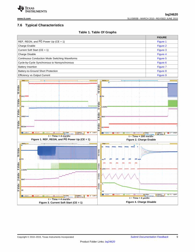
7.6 Typical Characteristics
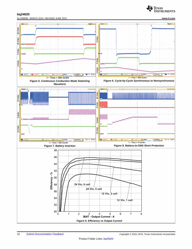
Table 1. Table Of GraphsFIGURE
REF, REGN, and PG Power Up (CE = 1) Figure 1Charge Enable Figure 2Current Soft Start (CE = 1) Figure 3Charge Disable Figure 4Continuous Conduction Mode Switching Waveforms Figure 5Cycle-by-Cycle Synchronous to Nonsynchronous Figure 6Battery Insertion Figure 7Battery-to-Ground Short Protection Figure 8Efficiency vs Output Current Figure 9
Figure 1. REF, REGN, and PG Power Up (CE = 1) Figure 2. Charge Enable
Figure 4. Charge DisableFigure 3. Current Soft Start (CE = 1)
Copyright © 2010–2015, Texas Instruments Incorporated Submit Documentation Feedback 9
Product Folder Links: bq24620
80
82
84
86
88
90
92
94
96
98
0 1 2 3 4 5 6 7 8
IBAT - Output Current - A
Eff
icie
ncy -
%
12 Vin, 1 cell
24 Vin, 5 cell
12 Vin, 2 cell
24 Vin, 6 cell
10 V
/div
10 V
/div
2A
/div
PH
VBAT
IL
t Time = 200 ms/div–
20
V/d
iv1
0 V
/div
2A
/div
PH
VBAT
IL
LDRV5 V
/div
t Time = 4 ms/div–
20
V/d
iv2
0 V
/div
5 V
/div
2A
/div
PH
LODRV
IL
HIDRV
t − Time = 200 ns/div
5 V
/div
5 V
/div
2A
/div
PH
LODRV
IL
t Time = 200 ns/div–
bq24620SLUS893B –MARCH 2010–REVISED JUNE 2015 www.ti.com
Figure 6. Cycle-by-Cycle Synchronous to NonsynchronousFigure 5. Continuous Conduction Mode SwitchingWaveform
Figure 8. Battery-to-GND Short ProtectionFigure 7. Battery Insertion
Figure 9. Efficiency vs Output Current
10 Submit Documentation Feedback Copyright © 2010–2015, Texas Instruments Incorporated
Product Folder Links: bq24620

VLOWV
VRECH
IPRECH & ITERM
PrechargeTime
Fastcharge Safety Time
Precharge
Current
Regulation
Phase
Fastcharge Current
Regulation Phase
Fastcharge Voltage
Regulation Phase Termination
Charge
Voltage
Charge
Current
Regulation Current
Regulation Voltage
bq24620www.ti.com SLUS893B –MARCH 2010–REVISED JUNE 2015
8 Detailed Description
8.1 OverviewThe bq24620 device is a stand-alone, integrated lithium phosphate battery charger. The device employs aswitched-mode synchronous buck PWM controller with constant switching frequency.
The bq24620 has a battery detect scheme that allows it to automatically detect the presence and absence of abattery. When the battery is detected, charging begins in one of three phases (depending upon battery voltage):precharge, constant current (fast-charge current regulation), and constant voltage (fast-charge voltageregulation). The device will terminate charging when the termination current threshold has been reached and willbegin a recharge cycle when the battery voltage has dropped below the recharge threshold (VRECHG). Constant(fastcharge) current and termination current can be configured through the ISET pin, allowing for flexibility inbattery charging profile. During charging, the integrated fault monitors of the device, such as battery overvoltageprotection, battery short detection (VBATSHT), thermal shutdown (internal TSHUT and TS pin), and input voltageprotection (VACOV and VUVLO), ensure battery safety.
The bq24620 has two status pins (STAT and PG) to indicate the charging status and input voltage (AC adapter)status. These pins can be used to drive LEDs or communicate with a host processor. Additionally, the PG pincan be used to drive external ACFET and BATFET.
Figure 10. Typical Charging Profile
Copyright © 2010–2015, Texas Instruments Incorporated Submit Documentation Feedback 11
Product Folder Links: bq24620

VCC
BTST
HIDRV
PH
REGN
LODRV
GND
TS
bq24620
CE
VFB
SRP
6V LDO
20XV(SRP-SRN)
COMP
ERROR
AMPLIFIER
1V
1.8 V
IBAT_ REG
SRN
STATE
MACHINE
LOGIC
BATTERY
DETECTION
LOGIC
VCC
PH
4.2 V
+_
BTST REFRESH
CE
145 degC
IC Tj TSHUT
SRN +100 mV
VCCSLEEP
LEVEL
SHIFTER
+
-
+
-
+
-
+
-
+
-
V(SRP -SRN ) CHG _OCP
+
-
160 % X IBAT _REG
SYNCHSRP-SRN
ISET
IBAT _ REGISET
ISET8
5 mV20X
BAT BAT _OVP
+
-
108 % X VBAT _REG
LTF
HTF
VREF
TCO +
-
+
-
SUSPEND
VCC ACOV+
-
VACOV
ENA _BIAS
VREF
STAT
STAT
3.3 V
LDOVCC
VFBLOWV
+
-
RCHRG
+-0.35V
+-1.675 V
VFB
LOWV
RCHRG
TERM
+
-
20XV(SRP-SRN)TERM
TERMINATE CHARGE
+
-
bq24620
+
-
+
-UVLO
VUVLO
VCC
SLEEP
UVLO
PWM
CONTROL
LOGIC
+
-
PWM
+
-
+
-+-
PG
+-
CHARGE
20 mA
DISCHARGE
CHARGE
8 mA
BAT _OVP
VOLTAGE
REFERENCE
VREF
ISET10
PG
5HR SafetyTimer
30 minutePrecharge
Timer
FAULT
FAULT
2 mA
1M
DISCHARGE
-
+
+
-
+
-COOL
WARMCOOL
WARM
20 mA
1.25 mV
bq24620SLUS893B –MARCH 2010–REVISED JUNE 2015 www.ti.com
8.2 Functional Block Diagram
12 Submit Documentation Feedback Copyright © 2010–2015, Texas Instruments Incorporated
Product Folder Links: bq24620

ISETTERM
SR
VI =
200 R´
ISETCHARGE
SR
VI =
20 R´
BAT
R2V = 1.8 V 1
R1
é ù´ +ê ú
ë û
bq24620www.ti.com SLUS893B –MARCH 2010–REVISED JUNE 2015
8.3 Feature Description
8.3.1 Battery Voltage RegulationThe bq24620 uses a high-accuracy voltage band gap and regulator for the charging voltage. The charge voltageis programmed through a resistor-divider from the battery to ground, with the midpoint tied to the VFB pin. Thevoltage at the VFB pin is regulated to 1.8 V, giving Equation 1 for the regulation voltage:
where• where R2 is connected from VFB to the battery and R1 is connected from VFB to GND. (1)
8.3.2 Battery Current RegulationThe ISET1 input sets the maximum charging current. Battery current is sensed by resistor RSR connectedbetween SRP and SRN. The full-scale differential voltage between SRP and SRN is 100 mV. Thus, for a 10-mΩsense resistor, the maximum charging current is 10 A. Equation 2 is for charge current:
(2)
VISET, the input voltage range of ISET, is from 0 to 2 V. The SRP and SRN pins are used to sense voltage acrossRSR with default value of 10 mΩ. However, resistors of other values can also be used. A larger sense resistorgives a larger sense voltage and a higher regulation accuracy, but at the expense of higher conduction loss.
8.3.3 PrechargeOn power up, if the battery voltage is below the VLOWV threshold, the bq24620 applies 125 mA to the battery. (1)
The precharge feature is intended to revive deeply discharged cells. If the VLOWV threshold is not reached within30 minutes of initiating precharge, the charger turns off and a FAULT is indicated on the status pins.
8.3.4 Charge Termination, Recharge, and Safety TimerThe bq24620 monitors the charging current during the voltage regulation phase. Termination is detected whilethe voltage on the VFB pin is higher than the VRECH threshold AND the charge current is less than the ITERMthreshold, which is 1/10th of programmed charge current, as calculated in Equation 3:
(3)
As a safety backup, the bq24620 also provides an internal 5-hour charge timer for fast charge.
A new charge cycle is initiated when one of the following conditions occurs:• The battery voltage falls below the recharge threshold.• A power-on reset (POR) event occurs.• CE is toggled.
8.3.5 Power UpThe bq24620 uses a SLEEP comparator to determine the source of power on the VCC pin, because VCC can besupplied either from the battery or the adapter. If the VCC voltage is greater than the SRN voltage, the bq24620enables ACFET and disables BATFET. If all other conditions are met for charging, the bq24620 then attempts tocharge the battery (see Enable and Disable Charging). If the SRN voltage is greater than VCC, indicating thatthe battery is the power source, bq24620 enters a low-quiescent-current (<15 μA) SLEEP mode to minimizecurrent drain from the battery.
If VCC is below the UVLO threshold, the device is disabled.(1) 125 mA (assuming a 10-mΩ sense resistor. 1.25 mV is regulated across SRP-SRN, regardless of the value of the sense resistor.)
Copyright © 2010–2015, Texas Instruments Incorporated Submit Documentation Feedback 13
Product Folder Links: bq24620

o
o o
1f =
2 L Cp
bq24620SLUS893B –MARCH 2010–REVISED JUNE 2015 www.ti.com
Feature Description (continued)8.3.6 Enable and Disable ChargingThe following conditions must be valid before charge is enabled:• CE is HIGH.• The device is not in VCCLOWV mode.• The device is not in SLEEP mode (that is, VCC > SRN) .• The VCC voltage is lower than the ac overvoltage threshold (VCC < VACOV).• 30-ms delay is complete after initial power up.• The REGN LDO and VREF LDO voltages are at the correct levels.• Thermal shutdown (TSHUT) is not valid.• TS fault is not detected.
Any of the following conditions stops ongoing charging:• CE is LOW.• Adapter is removed, causing the device to enter VCCLOWV or SLEEP mode.• Adapter voltage is less than 100 mV above battery.• Adapter is over voltage.• The REGN or VREF LDOs are overloaded.• TSHUT IC temperature threshold is reached (145°C on rising edge with 15°C hysteresis).• TS voltage goes out of range, indicating the battery temperature is too hot or too cold.• Safety timer times out.
8.3.7 Automatic Internal Soft-Start Charger CurrentThe charger automatically soft-starts the charger regulation current every time the charger goes into fast-chargeto ensure there is no overshoot or stress on the output capacitors or the power converter. The soft-start consistsof stepping up the charge regulation current into eight evenly divided steps up to the programmed chargecurrent. Each step lasts around 1.6 ms, for a typical rise time of 12.8 ms. No external components are neededfor this function.
8.3.8 Converter OperationThe synchronous buck PWM converter uses a fixed-frequency voltage mode with a feed-forward control scheme.A type-III compensation network allows using ceramic capacitors at the output of the converter. Thecompensation input stage is connected internally between the feedback output (FBO) and the error amplifierinput (EAI). The feedback compensation stage is connected between the error amplifier input (EAI) and erroramplifier output (EAO). The LC output filter is selected to give a resonant frequency of 10 kHz to 15 kHz forbq24620, where the resonant frequency, fo, is given by:
(4)
An internal sawtooth ramp is compared to the internal EAO error control signal to vary the duty cycle of theconverter. The ramp height is 7% of the input adapter voltage, making it always directly proportional to the inputadapter voltage. This cancels out any loop gain variation due to a change in input voltage, and simplifies the loopcompensation. The ramp is offset by 300 mV in order to allow zero-percent duty cycle when the EAO signal isbelow the ramp. The EAO signal is also allowed to exceed the sawtooth ramp signal in order to get a 100% duty-cycle PWM request. Internal gate-drive logic allows achieving 99.95% duty cycle while ensuring the N-channelupper device always has enough voltage to stay fully on. If the BTST pin to PH pin voltage falls below 4.2 V formore than three cycles, then the high-side N-channel power MOSFET is turned off and the low-side N-channelpower MOSFET is turned on to pull the PH node down and recharge the BTST capacitor. Then the high-sidedriver returns to 100% duty-cycle operation until the (BTST–PH) voltage is detected to fall low again due toleakage current discharging the BTST capacitor below 4.2 V, and the reset pulse is reissued.
The fixed-frequency oscillator keeps tight control of the switching frequency under all conditions of input voltage,battery voltage, charge current, and temperature, simplifying output filter design and keeping it out of the audiblenoise region. Also see Application and Implementation for how to select the inductor, capacitor, and MOSFET.
14 Submit Documentation Feedback Copyright © 2010–2015, Texas Instruments Incorporated
Product Folder Links: bq24620

bq24620www.ti.com SLUS893B –MARCH 2010–REVISED JUNE 2015
Feature Description (continued)8.3.9 Synchronous and Nonsynchronous OperationThe charger operates in synchronous mode when the SRP-SRN voltage is above 5 mV (0.5-A inductor currentfor a 10-mΩ sense resistor). During synchronous mode, the internal gate-drive logic ensures there is break-before-make complementary switching to prevent shoot-through currents. During the 30-ns dead time where bothFETs are off, the body diode of the low-side power MOSFET conducts the inductor current. Having the low-sideFET turn on keeps the power dissipation low, and allows safely charging at high currents. During synchronousmode, the inductor current is always flowing and the converter operates in continuous conduction mode (CCM),creating a fixed two-pole system.
The charger operates in nonsynchronous mode when the SRP-SRN voltage is below 5 mV (0.5-A inductorcurrent for a 10-mΩ sense resistor). The charger is forced into nonsynchronous mode when the battery voltage islower than 2 V or when the average SRP-SRN voltage is lower than 1.25 mV.
During nonsynchronous operation, the body diode of the low-side MOSFET can conduct the positive inductorcurrent after the high-side N-channel power MOSFET turns off. When the load current decreases and theinductor current drops to zero, the body diode is naturally turned off and the inductor current becomesdiscontinuous. This mode is called discontinuous conduction mode (DCM). During DCM, the low-side N-channelpower MOSFET turns on for around 80 ns when the bootstrap capacitor voltage drops below 4.2 V; then the low-side power MOSFET turns off and stays off until the beginning of the next cycle, where the high-side powerMOSFET is turned on again. The 80-ns low-side MOSFET on-time is required to ensure the bootstrap capacitoris always recharged and able to keep the high-side power MOSFET on during the next cycle. This is importantfor battery chargers, where unlike regular DC-DC converters, there is a battery load that maintains a voltage andcan both source and sink current. The 80-ns low-side pulse pulls the PH node (connection between high- andlow-side MOSFETs) down, allowing the bootstrap capacitor to recharge up to the REGN LDO value. After the 80ns, the low-side MOSFET is kept off to prevent negative inductor current from occurring.
At very low currents during nonsynchronous operation, there may be a small amount of negative inductor currentduring the 80-ns recharge pulse. The charge must be low enough to be absorbed by the input capacitance.Whenever the converter goes into zero-percent duty cycle, the high-side MOSFET does not turn on, and the low-side MOSFET does not turn on (only 80-ns recharge pulse) either, and there is almost no discharge from thebattery.
During the DCM mode, the loop response automatically changes and has a single-pole system at which the poleis proportional to the load current, because the converter does not sink current, and only the load provides acurrent sink. This means at very low currents the loop response is slower, as there is less sinking currentavailable to discharge the output voltage.
8.3.10 Cycle-by-Cycle Charge UndercurrentIf the SRP-SRN voltage decreases below 5 mV (the charger is also forced into nonsynchronous mode when theaverage SRP-SRN voltage is lower than 1.25 mV), the low-side FET is turned off for the remainder of theswitching cycle to prevent negative inductor current. During DCM, the low-side FET only turns on for around 80ns when the bootstrap capacitor voltage drops below 4.2 V to provide refresh charge for the bootstrap capacitor.This is important to prevent negative inductor current from causing a boost effect in which the input voltageincreases as power is transferred from the battery to the input capacitors, which leads to an overvoltage stresson the VCC node and potentially causes damage to the system.
8.3.11 Input Overvoltage Protection (ACOV)ACOV provides protection to prevent system damage due to high input voltage. Once the adapter voltagereaches the ACOV threshold, charge is disabled and the battery is switched to the system instead of the adapter.
8.3.12 Input Undervoltage Lockout (UVLO)The system must have a minimum VCC voltage to allow proper operation. This VCC voltage could come fromeither input the adapter orthe battery, if a conduction path exists from the battery to VCC through the high-sideNMOS body diode. When VCC is below the UVLO threshold, all circuits in the IC are disabled.
Copyright © 2010–2015, Texas Instruments Incorporated Submit Documentation Feedback 15
Product Folder Links: bq24620

bq24620SLUS893B –MARCH 2010–REVISED JUNE 2015 www.ti.com
Feature Description (continued)8.3.13 Battery Overvoltage ProtectionThe converter does not allow the high-side FET to turn on until the BAT voltage goes below 105% of theregulation voltage. This allows one-cycle response to an overvoltage condition, such as occurs when the load isremoved or the battery is disconnected. An 8-mA current sink from SRP/SRN to PGND is on only during chargeand allows discharging the stored output inductor energy that is transferred to the output capacitors. BATOVPalso suspends the safety timer.
8.3.14 Cycle-by-Cycle Charge Overcurrent ProtectionThe charger has a secondary cycle-to-cycle overcurrent protection. The charger monitors the charge current, andprevents the current from exceeding 160% of the programmed charge current. The high-side gate drive turns offwhen the overcurrent is detected, and automatically resumes when the current falls below the overcurrentthreshold.
8.3.15 Thermal Shutdown ProtectionThe QFN package has low thermal impedance, which provides good thermal conduction from the silicon to theambient, to keep junctions temperatures low. As an added level of protection, the charger converter turns off andself-protects whenever the junction temperature exceeds the TSHUT threshold of 145°C. The charger stays offuntil the junction temperature falls below 130°C. Then the charger soft-starts again if all other enable-chargeconditions are valid. Thermal shutdown also suspends the safety timer.
8.3.16 Temperature QualificationThe controller continuously monitors battery temperature by measuring the voltage between the TS pin andGND. A negative temperature coefficient thermistor (NTC) and an external voltage divider typically develop thisvoltage. The controller compares this voltage against its internal thresholds to determine if charging is allowed.To initiate a charge cycle, the battery temperature must be within the VLTF to VHTF thresholds. If batterytemperature is outside of this range, the controller suspends charge and the safety timer and waits until thebattery temperature is within the VLTF to VHTF range. During the charge cycle, the battery temperature must bewithin the VLTF to VTCO thresholds. If the battery temperature is outside of this range, the controller suspendscharge and the safety timer and waits until the battery temperature is within the VLTF to VHTF range. If the batterytemperature is between the VLTF and VCOOL thresholds or between the VHTF and VWARM thresholds, charge isautomatically reduced to ICHARGE/8. To avoid early termination during COOL/WARM condition, set ITERM ≤ICHARGE/10. The controller suspends charge by turning off the PWM charge FETs. Figure 11 and Figure 12summarize the operation.
16 Submit Documentation Feedback Copyright © 2010–2015, Texas Instruments Incorporated
Product Folder Links: bq24620

Temperature
ProgrammedCharge Current
1/8 x ProgrammedCharge Current
ChargeCurrent
ChargeSuspended
ICH
AR
GE
G/8
Ch
arg
e
Charge at ICHG
I/8
CH
AR
GE
Ch
arg
e
ChargeSuspended
VLTF VCOOLVWARM
VHTF/VTCO
(I )CHARGE
(I /8)CHARGE
CHARGE SUSPENDED CHARGE SUSPENDED
TEMPERATURE RANGE TOINITIATE CHARGE
TEMPERATURE RANGEDURING A CHARGE CYCLE
VHTF
GND
VTCO
GND
VREF VREF
CHARGE SUSPENDED CHARGE SUSPENDED
VLTF VLTF
CHARGE at I /8CHARGE CHARGE at I /8CHARGE
VWARM
CHARGE at I /8CHARGE CHARGE at I /8CHARGE
VCOOL
CHARGE at ICHARGE CHARGE at ICHARGE
VCOOL
VWARM
VLTF_HYS
VCOOL_HYS
VWARM_HYS
bq24620www.ti.com SLUS893B –MARCH 2010–REVISED JUNE 2015
Feature Description (continued)
Figure 11. TS, Thermistor Sense Thresholds
Figure 12. Typical Charge Current vs Temperature Profile
Assuming a 103AT NTC thermistor on the battery pack as shown in Figure 17, the values of RT1 and RT2 canbe determined by using Equation 5 and Equation 6:
Copyright © 2010–2015, Texas Instruments Incorporated Submit Documentation Feedback 17
Product Folder Links: bq24620

VREF
TS
RT2
RT1
RTH
103AT
bq24620
VREF
COOL
COOL
V1
VRT1 =
1 1+
RT2 RTH
-
VREF COOL WARM
COOL WARM
VREF VREFWARM COOL
WARM COOL
1 1V RTH RTH
V VRT2 =
V VRTH 1 RTH 1
V V
æ ö´ ´ ´ -ç ÷
è ø
æ öæ ö´ - - ´ -ç ÷ç ÷
è ø è ø
bq24620SLUS893B –MARCH 2010–REVISED JUNE 2015 www.ti.com
Feature Description (continued)
(5)
(6)
Figure 13. TS Resistor Network
For example, a 103AT NTC thermistor is used to monitor the battery pack temperature. Select TCOOL = 0ºC,TWARM = 60ºC. From the calculation and selecting a standard 5% resistor value, we can get RT1 = 2.2 kΩ, RT2 =6.8 kΩ, and TCOLD is –17ºC (target –20ºC); THOT is 77ºC (target 75ºC), and TCUT-OFF is 86ºC (target 80ºC). A smallRC filter is suggested to protect the TS pin from system-level ESD.
8.3.17 Timer Fault RecoveryThe bq24620 provides a recovery method to deal with timer fault conditions. The following summarizes thismethod:
Condition 1: The battery voltage is above the recharge threshold and a time-out fault occurs.
Recovery Method: The timer fault clears when the battery voltage falls below the recharge threshold, andbattery detection begins. Taking CE low, or a POR condition, also clears the fault.
Condition 2: The battery voltage is below the RECHARGE threshold and a time-out fault occurs.
Recovery Method: Under this scenario, the bq24620 applies the IFAULT current to the battery. This smallcurrent is used to detect a battery removal condition and remains on as long as the battery voltage stays belowthe recharge threshold. If the battery voltage goes above the recharge threshold, the bq24620 disables the faultcurrent and executes the recovery method described in Condition 1. Taking CE low, or a POR condition, alsoclears the fault.
8.3.18 PG OutputThe open-drain PG (power good) indicates whether the VCC voltage is valid or not. The open-drain FET turns onwhenever the bq24620 has a valid VCC input (not in UVLO or ACOV or SLEEP mode). The PG pin can be usedto drive an LED or communicate with the host processor.
18 Submit Documentation Feedback Copyright © 2010–2015, Texas Instruments Incorporated
Product Folder Links: bq24620

bq24620www.ti.com SLUS893B –MARCH 2010–REVISED JUNE 2015
Feature Description (continued)8.3.19 CE (Charge Enable)The CE digital input is used to disable or enable the charge process. A high-level signal on this pin enablescharge, provided all the other conditions for charge are met (see Enable and Disable Charging). A high-to-lowtransition on this pin also resets all timers and fault conditions. There is an internal 1-MΩ pulldown resistor on theCE pin, so if CE is floated, the charge does not turn on.
8.3.20 Charge Status OutputsThe open-drain STAT outputs indicate various charger operations as shown in Table 2. These status pins can beused to drive LEDs or communicate with the host processor. OFF indicates that the open-drain transistor isturned off.
Table 2. Stat Pin Definition For Bq24620CHARGE STATE STAT
Charge in progress ONCharge complete (PG = LOW) OFFSleep mode (PG = HIGH) OFFCharge suspend, timer fault, ACOV, battery absent BLINK (0.5 Hz)
Copyright © 2010–2015, Texas Instruments Incorporated Submit Documentation Feedback 19
Product Folder Links: bq24620

POR or RECHARGE
Enable 125-mA Charge,
Start 0.5-s timer
VFB > VRECH No
Battery Present,
Begin Charge
0.5-s timer
expired
Yes
No
Yes
Disable 125-mA
Charge
current, start 1-s timer
VFB < VLOWV No
Battery Present,
Begin Charge
1-s timer
expired
Yes
No
Yes
Disable 8-mA
discharge current
The battery detection routine runs on
power up, or if VFB falls below VRECH
due to removing a battery or
discharging a battery
Battery Absent
Apply 8-mA discharge
bq24620SLUS893B –MARCH 2010–REVISED JUNE 2015 www.ti.com
8.3.21 Battery DetectionFor applications with removable battery packs, the bq24620 provides a battery-absent detection scheme toreliably detect insertion or removal of battery packs. CE must be HIGH to enable battery detection function.
Figure 14. Battery Detection Flow Chart
Once the device has powered up, an 8-mA discharge current is applied to the SRN terminal. If the batteryvoltage falls below the LOWV threshold within 1 second, the discharge source is turned off, and the charger isturned on at low charge current (125 mA). If the battery voltage rises above the recharge threshold within 500ms, no battery is present and the cycle restarts. If either the 500-ms or 1-second timer times out before therespective thresholds are hit, a battery is detected and a charge cycle is initiated. See Maximum OutputCapacitance for more information.
20 Submit Documentation Feedback Copyright © 2010–2015, Texas Instruments Incorporated
Product Folder Links: bq24620

VRECH
VLOWV
BatteryInserted
Battery not Detected
tWAKE
Battery Detected
tLOWV_DEG t RECH_DEG
VREG
bq24620www.ti.com SLUS893B –MARCH 2010–REVISED JUNE 2015
Figure 15. Battery-Detect Timing Diagram
Copyright © 2010–2015, Texas Instruments Incorporated Submit Documentation Feedback 21
Product Folder Links: bq24620

bq24620SLUS893B –MARCH 2010–REVISED JUNE 2015 www.ti.com
8.4 Device Functional Modes
Figure 16. Device Operational Flow Chart
22 Submit Documentation Feedback Copyright © 2010–2015, Texas Instruments Incorporated
Product Folder Links: bq24620

N
VREF
CE
VFBTS
VCC HIDRV
N
PH
BTST
REGN
LODRV
GND
SRP
SRN
PACK+
PACK-
ADAPTER +
ADAPTER -
C4
C7
Q4
SiR426
Q5
SiR426
C6
L1
8.2 µH*D1
BAT54
C5
C10
0.1 µF
C9
10 µF
VREF
Pack
Thermistor
Sense
bq24620
VREF
ISET
STAT
VBAT
R9
9.31 kW
R10
430 kW
R1
100 kW
PG
ADAPTER +Cff
22 pF
0.1 µF
1 µF
1 µF1 µF
RSR
0.010 Ω
C11
0.1 µF
C12
10 µF*
C13
10 µF*
R2
900 kW
R13 10 kW
R14 10 kW
R7
100 kW
R8
22.1 kW
PwrPad
D2
MBRS540T3
C8
10 µFR6
10 W
D3
D4
R5
100 W
0.1 Fμ
R112 W
C22.2 µF
bq24620www.ti.com SLUS893B –MARCH 2010–REVISED JUNE 2015
9 Application and Implementation
NOTEInformation in the following applications sections is not part of the TI componentspecification, and TI does not warrant its accuracy or completeness. TI’s customers areresponsible for determining suitability of components for their purposes. Customers shouldvalidate and test their design implementation to confirm system functionality.
9.1 Application InformationThe bq24620 battery charger is ideal for high current charging (up to 10 A) and can charge battery packsconsisting of single cells or multiple cells in series. The bq24620EVM evaluation module is a complete chargemodule for evaluating the bq24620. The application curves were taken using the bq24620EVM. Refer to the EVMuser's guide (SLUU410) for EVM information.
9.2 Typical Application
NOTE: VIN = 28 V, BAT = 5-cell Li-Phosphate, Icharge = 3 A, Iprecharge = 0.125 A, Iterm = 0.3 A
Figure 17. Typical System Schematic
9.2.1 Design RequirementsFor this design example, use the parameters listed in Table 3 as the input parameters.
Table 3. Design ParametersDESIGN PARAMETER EXAMPLE VALUE
AC adapter voltage (VIN) 28 VBattery charge voltage (number of cells in series) 18 V (5 cells)Battery charge current (during constant current phase) 3 APrecharge current 0.125 ATermination current 0.3 A
Copyright © 2010–2015, Texas Instruments Incorporated Submit Documentation Feedback 23
Product Folder Links: bq24620

æ öD = -ç ÷
ç ÷è ø
2
BATo BAT2
INs
V1V V
V8LCf
RIPPLECOUT RIPPLE
II = 0.29 I
2 3
» ´
´
CIN CHGI = I D (1 D)´ ´ -
INRIPPLE
S
V D (1 D)I =
f L
´ ´ -
´
SAT CHG RIPPLEI I + (1/2) I³
bq24620SLUS893B –MARCH 2010–REVISED JUNE 2015 www.ti.com
9.2.2 Detailed Design Procedure
9.2.2.1 Inductor SelectionThe bq24620 has a 300-kHz switching frequency to allow the use of small inductor and capacitor values.Inductor saturation current must be higher than the charging current (ICHARGE) plus half the ripple current (IRIPPLE):
(7)
The inductor ripple current depends on input voltage (VIN), duty cycle (D = VOUT/VIN), switching frequency (fS) andinductance (L):
(8)
The maximum inductor ripple current happens with D = 0.5. For example, the battery-charging voltage range isfrom 2.8 V to 14.4 V for a four-cell battery pack. For 20-V adapter voltage, 10-V battery voltage gives themaximum inductor ripple current.
Usually, inductor ripple is designed in the range of 20%–40% of maximum charging current as a trade-offbetween inductor size and efficiency for a practical design.
The bq24620 has cycle-by-cycle charge undercurrent protection (UCP) by monitoring the charging-currentsensing resistor to prevent negative inductor current. The typical UCP threshold is 5 mV falling edge,corresponding to 0.5-A falling edge for a 10-mΩ charging-current-sensing resistor.
9.2.2.2 Input CapacitorThe input capacitor must have enough ripple current rating to absorb input switching-ripple current. The worst-case RMS ripple current is half of the charging current when duty cycle is 0.5. If the converter does not operateat 50% duty cycle, then the worst-case capacitor RMS current ICIN occurs where the duty cycle is closest to 50%and can be estimated by the following equation:
(9)
A low-ESR ceramic capacitor such as X7R or X5R is preferred for the input-decoupling capacitor and must beplaced as close as possible to the drain of the high-side MOSFET and source of the low-side MOSFET. Thevoltage rating of the capacitor must be higher than the normal input voltage level. A 25-V rating or highercapacitor is preferred for 20-V input voltage. A 20-µF capacitor is suggested for typical of 3-A to 4-A chargingcurrent.
9.2.2.3 Output CapacitorThe output capacitor also must have enough ripple current rating to absorb the output switching-ripple current.The output capacitor RMS current ICOUT is given:
(10)
The output capacitor voltage ripple can be calculated as follows:
(11)
At certain input and output voltage and switching frequency, the voltage ripple can be reduced by increasing theoutput filter LC.
The bq24620 has an internal loop compensator. To get good loop stability, the resonant frequency of the outputinductor and output capacitor must be designed from 10 kHz to 15 kHz. The preferred ceramic capacitor is 25 V,X7R, or X5R for 4-cell applications.
24 Submit Documentation Feedback Copyright © 2010–2015, Texas Instruments Incorporated
Product Folder Links: bq24620

ICLoss_driver IN g_total sP V Q f= × ×
2bottom CHG DS(on)P = (1 D) I R- ´ ´
REGN plt plton off
on off
V V VI = , I =
R R
-
SW GD GS
1Q = Q + Q
2´
SW SWon off
on off
Q Qt = , t =
I I
( )2top CHG DS(on) IN CHG on off S
1P = D I R + V I t + t f
2´ ´ ´ ´ ´ ´
top DS(on) GD bottom DS(on) GFOM = R Q FOM = R Q´ ´
bq24620www.ti.com SLUS893B –MARCH 2010–REVISED JUNE 2015
9.2.2.4 Power MOSFET SelectionTwo external N-channel MOSFETs are used for a synchronous switching battery charger. The gate drivers areinternally integrated into the IC with 6 V of gate drive voltage. 30-V or higher voltage rating MOSFETs arepreferred for 20-V input voltage, and 40-V MOSFETs are preferred for 20-V to 28-V input voltage.
Figure-of-merit (FOM) is usually used for selecting the proper MOSFET, based on a tradeoff between theconduction loss and switching loss. For the top-side MOSFET, FOM is defined as the product of the MOSFETON-resistance, rDS(on), and the gate-to-drain charge, QGD. For the bottom-side MOSFET, FOM is defined as theproduct of the MOSFET ON-resistance, rDS(on), and the total gate charge, QG.
(12)
The lower the FOM value, the lower the total power loss. Usually lower rDS(on) has higher cost with the samepackage size.
The top-side MOSFET loss includes conduction loss and switching loss. It is a function of duty cycle (D =VOUT/VIN), charging current (ICHARGE), MOSFET ON-resistance rDS(on)), input voltage (VIN), switching frequency(fS), turnon time (ton), and turnoff time (toff):
(13)
The first item represents the conduction loss. Usually MOSFET rDS(on) increases by 50% with 100ºC junctiontemperature rise. The second term represents the switching loss. The MOSFET turnon and turnoff times aregiven by:
(14)
where Qsw is the switching charge, Ion is the turnon gate-driving current, and Ioff is the turnoff gate-driving current.If the switching charge is not given in the MOSFET data sheet, it can be estimated by gate-to-drain charge (QGD)and gate-to-source charge (QGS):
(15)
Total gate-driving current can be estimated by the REGN voltage (VREGN), MOSFET plateau voltage (Vplt), totalturnon gate resistance (Ron), and turnoff gate resistance Roff) of the gate driver:
(16)
The conduction loss of the bottom-side MOSFET is calculated with the following equation when it operates insynchronous continuous conduction mode:
(17)
If the SRP–SRN voltage decreases below 5 mV (the charger is also forced into nonsynchronous mode when theaverage SRP–SRN voltage is lower than 1.25 mV), the low-side FET is turned off for the remainder of theswitching cycle to prevent negative inductor current.
As a result, all the freewheeling current goes through the body diode of the bottom-side MOSFET. The maximumcharging current in nonsynchronous mode can be up to 0.9 A (0.5 A typical) for a 10-mΩ charging-current-sensing resistor, considering IC tolerance. Choose the bottom-side MOSFET with either an internal Schottky orbody diode capable of carrying the maximum nonsynchronous mode charging current.
MOSFET gate-driver power loss contributes to the dominant losses on controller IC when the buck converter isswitching. Choosing a MOSFET with a small Qg_total reduces the IC power loss to avoid thermal shutdown.
where• Qg_total is the total gate charge for both upper and lower MOSFETs at 6-V VREGN (18)
The VREF load current is another component of the VCC input current (do not overload VREF), where total ICloss can be described by following equations:
Copyright © 2010–2015, Texas Instruments Incorporated Submit Documentation Feedback 25
Product Folder Links: bq24620

o
o o
1f =
2 L Cp
R12 W
C12.2 mF
D1
C20.1-1 mF
R24.7-30WAdapter
connectorVCC pin
(2010)(1206)
VREF IN VREF VREF
ICLOSS ICLOSS _ driver VREF Quiescent
P (V V ) I
P P P P
= - ×
= + +
bq24620SLUS893B –MARCH 2010–REVISED JUNE 2015 www.ti.com
(19)
9.2.2.5 Input Filter DesignDuring adapter hot plug-in, the parasitic inductance and input capacitor from the adapter cable form a second-order system. The voltage spike at the VCC pin may be beyond the IC maximum voltage rating and damage theIC. The input filter must be carefully designed and tested to prevent an overvoltage event on VCC pin.
There are several methods to damping or limiting the overvoltage spike during adapter hot plug-in. An electrolyticcapacitor with high ESR as an input capacitor can damp the overvoltage spike well below the IC maximum pin-voltage rating. A high-current-capability TVS Zener diode can also limit the overvoltage level to an IC-safe level.However, these two solutions may not have low cost or small size.
A cost-effective and small-size solution is shown in Figure 18. R1 and C1 comprise a damping RC network todamp the hot plug-in oscillation. As a result, the overvoltage spike is limited to a safe level. D1 is used forreverse voltage protection for the VCC pin (it can be the input Schottky diode or the body diode of the inputACFET). C2 is a VCC pin-decoupling capacitor, and it must be placed as close as possible to the VCC pin. R2and C2 form a damping RC network to further protect the IC from high-dv/dt and high-voltage spikes. The C2value must be less than the C1 value so R1 can be dominant over the ESR of C1 to get enough damping effectfor hot plug-in. R1 and R2 packages must be sized to handle the inrush-current power loss according to theresistor manufacturer’s data sheet. The filter component values always must be verified with the real application,and minor adjustments may be needed to fit in the real application circuit.
Figure 18. Input Filter
9.2.2.6 Inductor, Capacitor, and Sense Resistor Selection GuidelinesThe bq24620 provides internal loop compensation. With this scheme, best stability occurs when the LC resonantfrequency, fo, is approximately 10 kHz to 15 kHz per Equation 20:
(20)
Table 4 provides a summary of typical LC components for various charge currents
Table 4. Typical Inductor, Capacitor, and Sense Resistor Values as a Function of Charge CurrentCHARGE CURRENT 2 A 4 A 6 A 8 A 10 AOutput inductor LO 8.2 μH 8.2 μH 5.6 μH 4.7 μH 4.7 μHOutput capacitor CO 20 μF 20 μF 20 μF 40 μF 40 μFSense resistor 10 mΩ 10 mΩ 10 mΩ 10 mΩ 10 mΩ
26 Submit Documentation Feedback Copyright © 2010–2015, Texas Instruments Incorporated
Product Folder Links: bq24620

MAX
8mA 1secC = = 930 F
500k1.425 1+
100k
´m
é ù´ ê úë û
DISCH DISCHMAX
2
1
I tC =
R1.425 1+
R
´
é ù´ ê ú
ë û
bq24620www.ti.com SLUS893B –MARCH 2010–REVISED JUNE 2015
Table 5. Component List for Typical System Circuit of Figure 17PART DESIGNATOR QTY DESCRIPTIONQ4, Q5 2 N-channel MOSFET, 40 V, 30 A, PowerPAK SO-8, Vishay-Siliconix, SiR426DND1 1 Diode, dual Schottky, 30 V, 200 mA, SOT23, Fairchild, BAT54CD2 1 Schottky diode, 40 V, 5 A, SMC, ON Semiconductor, MBRS540T3RSR 2 Sense resistor, 10 mΩ, 1%, 1 W, 2010, Vishay-Dale, WSL2010R0100FL1 1 Inductor, 6.8 μH, 5.5 A, Vishay-Dale, IHLP2525CZC8, C9, C12, C13 4 Capacitor, ceramic, 10 μF, 35 V, 10%, X7RC2 1 Capacitor, ceramic, 2.2 µF, 50 V, 10%, X7RC4, C5 2 Capacitor, ceramic, 1 μF, 16 V, 10%, X7RC7 1 Capacitor, ceramic, 1 µF, 50 V, 10%, X7RC1, C6, C11 4 Capacitor, ceramic, 0.1 μF, 16 V, 10%, X7RCff 1 Capacitor, ceramic, 22 pF, 35 V, 10%, X7RC10 1 Capacitor, ceramic, 0.1 μF, 50 V, 10%R1, R7 2 Resistor, chip, 100 kΩ, 1/16 W, 0.5%R2 1 Resistor, chip, 900 kΩ, 1/16 W, 0.5%R8 1 Resistor, chip, 22.1 kΩ, 1/16 W, 0.5%R9 1 Resistor, chip, 9.31 kΩ, 1/16 W, 1%R10 1 Resistor, chip, 430 kΩ, 1/16 W, 1%R11 1 Resistor, chip, 2 Ω, 1 W, 5%R13, R14 2 Resistor, chip, 10 kΩ, 1/16 W, 5%R5 1 Resistor, chip, 100 Ω, 1/16 W, 0.5%R6 1 Resistor, chip, 10 Ω, 1 W, 5%D3, D4 2 LED diode, green, 2.1 V, 10 mΩ, Vishay-Dale, WSL2010R0100F
9.2.2.7 Maximum Output CapacitanceCare must be taken that the total output capacitance at the battery node is not so large that the discharge currentsource cannot pull the voltage below the LOWV threshold during the 1-second discharge time. The maximumoutput capacitance can be calculated as seen in Equation 21:
where• CMAX is the maximum output capacitance.• IDISCH is the discharge current.• tDISCH is the discharge time.• R2 and R1 are the voltage feedback resistors from the battery to the VFB pin. (21)
The 1.425 factor is the difference between the RECHARGE and the LOWV thresholds at the VFB pin.
EXAMPLEFor a 3-cell Li+ charger, with R2 = 500 kΩ, R1 = 100 kΩ (giving 10.8 V for voltage regulation), IDISCH = 8 mA,tDISCH = 1 second,
(22)
Based on these calculations, no more than 930 μF should be allowed on the battery node for proper operation ofthe battery detection circuit.
Copyright © 2010–2015, Texas Instruments Incorporated Submit Documentation Feedback 27
Product Folder Links: bq24620

bq24620SLUS893B –MARCH 2010–REVISED JUNE 2015 www.ti.com
9.2.3 Application Curves
VIN: 28 V VBAT: 16 V ICHG = 3 A VIN: 28 V VBAT: 16 V ICHG = 3 A
Figure 19. Continuous Conduction Mode Figure 20. Battery Charging Soft Start(by Asserting CE Low to High)
28 Submit Documentation Feedback Copyright © 2010–2015, Texas Instruments Incorporated
Product Folder Links: bq24620

bq24620www.ti.com SLUS893B –MARCH 2010–REVISED JUNE 2015
10 Power Supply RecommendationsFor proper operation of bq24620, VCC must be from 5 V to 28 V. To begin charging, VCC must be higher thanSRN by at least 500 mV (otherwise, the device will be in sleep mode). TI recommends an input voltage of atleast 1.5 V to 2 V higher than the battery voltage, taking into consideration the DC losses in the high-side FET(Rdson), inductor (DCR), the input diode drop, and battery sense resistor (between SRP and SRN). Power limitfor the input supply must be greater than the maximum power required for battery charging.
11 Layout
11.1 Layout GuidelinesThe switching node rise and fall times must be minimized for minimum switching loss. Proper layout of thecomponents to minimize the high-frequency current-path loop (see Figure 21) is important to prevent electricaland magnetic field radiation and high-frequency resonant problems. The following is a PCB layout priority list forproper layout. Layout of the PCB according to this specific order is essential.1. Place the input capacitor as close as possible to the switching MOSFET supply and ground connections, and
use the shortest possible copper trace connection. These parts should be placed on the same layer of thePCB instead of on different layers, using vias to make this connection.
2. The IC must be placed close to the switching MOSFET gate terminals, keeping the gate-drive signal tracesshort for a clean MOSFET drive. The IC can be placed on the other side of the PCB from the switchingMOSFETs.
3. Place the inductor input terminal as close as possible to switching MOSFET output terminal. Minimize thecopper area of this trace to lower electrical and magnetic field radiation, but make the trace wide enough tocarry the charging current. Do not use multiple layers in parallel for this connection. Minimize parasiticcapacitance from this area to any other trace or plane.
4. The charging-current-sensing resistor must be placed right next to the inductor output. Route the sense leadsconnected across the sensing resistor back to the IC in same layer, close to each other (minimize loop area),and do not route the sense leads through a high-current path (see Figure 22 for Kelvin connection for bestcurrent accuracy). Place the decoupling capacitor on these traces next to the IC.
5. Place the output capacitor next to the sensing-resistor output and ground.6. The output capacitor ground connections must be tied to the same copper that connects to the input
capacitor ground before connecting to system ground.7. Route the analog ground separately from the power ground and use a single ground connection to tie the
charger power ground to the charger analog ground. Just beneath the IC, use the copper pour for analogground, but avoid power pins to reduce inductive and capacitive noise coupling. Connect analog ground toGND. Connect the analog ground and power ground together using the thermal pad as the single groundconnection point, or use a 0-Ω resistor to tie analog ground to power ground (the thermal pad should tie toanalog ground in this case). A star-connection under the thermal pad is highly recommended.
8. It is critical to solder the exposed thermal pad on the back of the IC package to the PCB ground. Ensure thatthere are sufficient thermal vias directly under the IC, connecting to the ground plane on the other layers.
9. Place decoupling capacitors next to the IC pins to make trace connections as short as possible.10. All via sizes and numbers must be enough for a given current path.
See the EVM design (SLUU410) for the recommended component placement with trace and via locations.
For QFN information, see SCBA017 and SLUA271.
Copyright © 2010–2015, Texas Instruments Incorporated Submit Documentation Feedback 29
Product Folder Links: bq24620

Current Direction
To SRP - SRN pin
RSNS
Current Sensing Direction
High
Frequency
Current
Path
L1 R1
C3C1
C2PGND
SW VBAT
BATVIN
bq24620SLUS893B –MARCH 2010–REVISED JUNE 2015 www.ti.com
11.2 Layout Example
Figure 21. High-Frequency Current Path
Figure 22. Sensing Resistor PCB Layout
30 Submit Documentation Feedback Copyright © 2010–2015, Texas Instruments Incorporated
Product Folder Links: bq24620

bq24620www.ti.com SLUS893B –MARCH 2010–REVISED JUNE 2015
12 Device and Documentation Support
12.1 Device Support
12.1.1 Third-Party Products DisclaimerTI'S PUBLICATION OF INFORMATION REGARDING THIRD-PARTY PRODUCTS OR SERVICES DOES NOTCONSTITUTE AN ENDORSEMENT REGARDING THE SUITABILITY OF SUCH PRODUCTS OR SERVICESOR A WARRANTY, REPRESENTATION OR ENDORSEMENT OF SUCH PRODUCTS OR SERVICES, EITHERALONE OR IN COMBINATION WITH ANY TI PRODUCT OR SERVICE.
12.2 Documentation Support
12.2.1 Related DocumentationFor related documentation, see the following:• bq24600/20/40 EVM (HPA421) Multi Cell Synchronous Switch-Mode Charger, SLUU410• Quad Flatpack No-Lead Logic Packages, SCBA017• QFN/SON PCB Attachment, SLUA271
12.3 Community ResourcesThe following links connect to TI community resources. Linked contents are provided "AS IS" by the respectivecontributors. They do not constitute TI specifications and do not necessarily reflect TI's views; see TI's Terms ofUse.
TI E2E™ Online Community TI's Engineer-to-Engineer (E2E) Community. Created to foster collaborationamong engineers. At e2e.ti.com, you can ask questions, share knowledge, explore ideas and helpsolve problems with fellow engineers.
Design Support TI's Design Support Quickly find helpful E2E forums along with design support tools andcontact information for technical support.
12.4 TrademarksE2E is a trademark of Texas Instruments.All other trademarks are the property of their respective owners.
12.5 Electrostatic Discharge CautionThese devices have limited built-in ESD protection. The leads should be shorted together or the device placed in conductive foamduring storage or handling to prevent electrostatic damage to the MOS gates.
12.6 GlossarySLYZ022 — TI Glossary.
This glossary lists and explains terms, acronyms, and definitions.
13 Mechanical, Packaging, and Orderable InformationThe following pages include mechanical, packaging, and orderable information. This information is the mostcurrent data available for the designated devices. This data is subject to change without notice and revision ofthis document. For browser-based versions of this data sheet, refer to the left-hand navigation.
Copyright © 2010–2015, Texas Instruments Incorporated Submit Documentation Feedback 31
Product Folder Links: bq24620

PACKAGE OPTION ADDENDUM
www.ti.com 7-Apr-2015
Addendum-Page 1
PACKAGING INFORMATION
Orderable Device Status(1)
Package Type PackageDrawing
Pins PackageQty
Eco Plan(2)
Lead/Ball Finish(6)
MSL Peak Temp(3)
Op Temp (°C) Device Marking(4/5)
Samples
BQ24620RVAR ACTIVE VQFN RVA 16 3000 Green (RoHS& no Sb/Br)
CU NIPDAU Level-2-260C-1 YEAR -40 to 85 OAR
BQ24620RVAT ACTIVE VQFN RVA 16 250 Green (RoHS& no Sb/Br)
CU NIPDAU Level-2-260C-1 YEAR -40 to 85 OAR
(1) The marketing status values are defined as follows:ACTIVE: Product device recommended for new designs.LIFEBUY: TI has announced that the device will be discontinued, and a lifetime-buy period is in effect.NRND: Not recommended for new designs. Device is in production to support existing customers, but TI does not recommend using this part in a new design.PREVIEW: Device has been announced but is not in production. Samples may or may not be available.OBSOLETE: TI has discontinued the production of the device.
(2) Eco Plan - The planned eco-friendly classification: Pb-Free (RoHS), Pb-Free (RoHS Exempt), or Green (RoHS & no Sb/Br) - please check http://www.ti.com/productcontent for the latest availabilityinformation and additional product content details.TBD: The Pb-Free/Green conversion plan has not been defined.Pb-Free (RoHS): TI's terms "Lead-Free" or "Pb-Free" mean semiconductor products that are compatible with the current RoHS requirements for all 6 substances, including the requirement thatlead not exceed 0.1% by weight in homogeneous materials. Where designed to be soldered at high temperatures, TI Pb-Free products are suitable for use in specified lead-free processes.Pb-Free (RoHS Exempt): This component has a RoHS exemption for either 1) lead-based flip-chip solder bumps used between the die and package, or 2) lead-based die adhesive used betweenthe die and leadframe. The component is otherwise considered Pb-Free (RoHS compatible) as defined above.Green (RoHS & no Sb/Br): TI defines "Green" to mean Pb-Free (RoHS compatible), and free of Bromine (Br) and Antimony (Sb) based flame retardants (Br or Sb do not exceed 0.1% by weightin homogeneous material)
(3) MSL, Peak Temp. - The Moisture Sensitivity Level rating according to the JEDEC industry standard classifications, and peak solder temperature.
(4) There may be additional marking, which relates to the logo, the lot trace code information, or the environmental category on the device.
(5) Multiple Device Markings will be inside parentheses. Only one Device Marking contained in parentheses and separated by a "~" will appear on a device. If a line is indented then it is a continuationof the previous line and the two combined represent the entire Device Marking for that device.
(6) Lead/Ball Finish - Orderable Devices may have multiple material finish options. Finish options are separated by a vertical ruled line. Lead/Ball Finish values may wrap to two lines if the finishvalue exceeds the maximum column width.
Important Information and Disclaimer:The information provided on this page represents TI's knowledge and belief as of the date that it is provided. TI bases its knowledge and belief on informationprovided by third parties, and makes no representation or warranty as to the accuracy of such information. Efforts are underway to better integrate information from third parties. TI has taken andcontinues to take reasonable steps to provide representative and accurate information but may not have conducted destructive testing or chemical analysis on incoming materials and chemicals.TI and TI suppliers consider certain information to be proprietary, and thus CAS numbers and other limited information may not be available for release.

PACKAGE OPTION ADDENDUM
www.ti.com 7-Apr-2015
Addendum-Page 2
In no event shall TI's liability arising out of such information exceed the total purchase price of the TI part(s) at issue in this document sold by TI to Customer on an annual basis.

TAPE AND REEL INFORMATION
*All dimensions are nominal
Device PackageType
PackageDrawing
Pins SPQ ReelDiameter
(mm)
ReelWidth
W1 (mm)
A0(mm)
B0(mm)
K0(mm)
P1(mm)
W(mm)
Pin1Quadrant
BQ24620RVAR VQFN RVA 16 3000 330.0 12.4 3.75 3.75 1.15 8.0 12.0 Q1
BQ24620RVAT VQFN RVA 16 250 180.0 12.4 3.75 3.75 1.15 8.0 12.0 Q1
PACKAGE MATERIALS INFORMATION
www.ti.com 7-Apr-2015
Pack Materials-Page 1

*All dimensions are nominal
Device Package Type Package Drawing Pins SPQ Length (mm) Width (mm) Height (mm)
BQ24620RVAR VQFN RVA 16 3000 367.0 367.0 35.0
BQ24620RVAT VQFN RVA 16 250 210.0 185.0 35.0
PACKAGE MATERIALS INFORMATION
www.ti.com 7-Apr-2015
Pack Materials-Page 2


IMPORTANT NOTICE
Texas Instruments Incorporated and its subsidiaries (TI) reserve the right to make corrections, enhancements, improvements and otherchanges to its semiconductor products and services per JESD46, latest issue, and to discontinue any product or service per JESD48, latestissue. Buyers should obtain the latest relevant information before placing orders and should verify that such information is current andcomplete. All semiconductor products (also referred to herein as “components”) are sold subject to TI’s terms and conditions of salesupplied at the time of order acknowledgment.TI warrants performance of its components to the specifications applicable at the time of sale, in accordance with the warranty in TI’s termsand conditions of sale of semiconductor products. Testing and other quality control techniques are used to the extent TI deems necessaryto support this warranty. Except where mandated by applicable law, testing of all parameters of each component is not necessarilyperformed.TI assumes no liability for applications assistance or the design of Buyers’ products. Buyers are responsible for their products andapplications using TI components. To minimize the risks associated with Buyers’ products and applications, Buyers should provideadequate design and operating safeguards.TI does not warrant or represent that any license, either express or implied, is granted under any patent right, copyright, mask work right, orother intellectual property right relating to any combination, machine, or process in which TI components or services are used. Informationpublished by TI regarding third-party products or services does not constitute a license to use such products or services or a warranty orendorsement thereof. Use of such information may require a license from a third party under the patents or other intellectual property of thethird party, or a license from TI under the patents or other intellectual property of TI.Reproduction of significant portions of TI information in TI data books or data sheets is permissible only if reproduction is without alterationand is accompanied by all associated warranties, conditions, limitations, and notices. TI is not responsible or liable for such altereddocumentation. Information of third parties may be subject to additional restrictions.Resale of TI components or services with statements different from or beyond the parameters stated by TI for that component or servicevoids all express and any implied warranties for the associated TI component or service and is an unfair and deceptive business practice.TI is not responsible or liable for any such statements.Buyer acknowledges and agrees that it is solely responsible for compliance with all legal, regulatory and safety-related requirementsconcerning its products, and any use of TI components in its applications, notwithstanding any applications-related information or supportthat may be provided by TI. Buyer represents and agrees that it has all the necessary expertise to create and implement safeguards whichanticipate dangerous consequences of failures, monitor failures and their consequences, lessen the likelihood of failures that might causeharm and take appropriate remedial actions. Buyer will fully indemnify TI and its representatives against any damages arising out of the useof any TI components in safety-critical applications.In some cases, TI components may be promoted specifically to facilitate safety-related applications. With such components, TI’s goal is tohelp enable customers to design and create their own end-product solutions that meet applicable functional safety standards andrequirements. Nonetheless, such components are subject to these terms.No TI components are authorized for use in FDA Class III (or similar life-critical medical equipment) unless authorized officers of the partieshave executed a special agreement specifically governing such use.Only those TI components which TI has specifically designated as military grade or “enhanced plastic” are designed and intended for use inmilitary/aerospace applications or environments. Buyer acknowledges and agrees that any military or aerospace use of TI componentswhich have not been so designated is solely at the Buyer's risk, and that Buyer is solely responsible for compliance with all legal andregulatory requirements in connection with such use.TI has specifically designated certain components as meeting ISO/TS16949 requirements, mainly for automotive use. In any case of use ofnon-designated products, TI will not be responsible for any failure to meet ISO/TS16949.
Products ApplicationsAudio www.ti.com/audio Automotive and Transportation www.ti.com/automotiveAmplifiers amplifier.ti.com Communications and Telecom www.ti.com/communicationsData Converters dataconverter.ti.com Computers and Peripherals www.ti.com/computersDLP® Products www.dlp.com Consumer Electronics www.ti.com/consumer-appsDSP dsp.ti.com Energy and Lighting www.ti.com/energyClocks and Timers www.ti.com/clocks Industrial www.ti.com/industrialInterface interface.ti.com Medical www.ti.com/medicalLogic logic.ti.com Security www.ti.com/securityPower Mgmt power.ti.com Space, Avionics and Defense www.ti.com/space-avionics-defenseMicrocontrollers microcontroller.ti.com Video and Imaging www.ti.com/videoRFID www.ti-rfid.comOMAP Applications Processors www.ti.com/omap TI E2E Community e2e.ti.comWireless Connectivity www.ti.com/wirelessconnectivity
Mailing Address: Texas Instruments, Post Office Box 655303, Dallas, Texas 75265Copyright © 2016, Texas Instruments Incorporated