boost converter with continuous output current for … converter with continuous output current for...
TRANSCRIPT

Boost converter with continuous output current for large power applications
YU. KRASNIKOV Power Electronics Co., Ltd.
Polevaya St., 8-71, Novosibirsk, 630128 RUSSIA
Abstract: - A new boost converter with a continuous output current has been proposed. It does not require an output capacitor with high current capability. Basic relationships are derived, advantages of the new solution are described and application areas are specified. Keywords: - Boost converter, DC/DC converter, DC power supply, Distribution of electrical energy. 1 Introduction Unlike buck converters, boost converters are rarely used for large power applications. The main reason is that a conventional boost converter does not perfectly match a load: its output current is 100% modulated, therefore an output filter capacitor, sometimes of a large value and high current capability is required. A new boost converter with a continuous output current has been developed for the case when the last circumstance becomes critical. 2 Problem Formulation In civil and naval engineering the rapidly growing power consumption and number of consumers is a major concern. The increased demands of comfort, safety and maneuverability also influence the availability, reliability and maintainability (ARM) requirements of the energy system [1]. As a rule, buck converters are used in distribution system of electrical energy to provide DC controlled voltage. Conventional boost converters are not used for large power conversion in DC distribution system due to their principal disadvantage of work. It is possible to allocate two time intervals in each period of work of a conventional boost converter. In the first time interval when a switch is ON, there is an accumulation of energy in inductor. At this time a load is supplied by the energy stored in an output capacitor. In the second time interval when a switch is OFF, there is a transfer of energy stored in inductor to a load and an output capacitor. For reduction of output voltage ripples and/or reduction of value of an output capacitor it is necessary to
provide conditions at which the output current is continuous independently of switch state. 3 Problem Solution 3.1 Comparison to a previous art A short comparison of a conventional buck, boost and invented converters, with respect to input and output current modulation, is given in the Table 1. For all 3 cases current deviations, produced by a finite inductance of a main inductor, are neglected. For a conventional buck and boost converters either input or output current is interrupted by the power switch, while for the invented boost converter output current is constant and input current is 50% modulated. Table 1: Input and output current modulations
in different converters
Topology Input
current modulation
Output current
modulation Conventional buck converter
100% 0%
Conventional boost converter
0% 100%
Invented CCM boost converter
50% 0%
Fig. 1b shows the invented CCM (Continuous Current Mode) boost converter circuit [1], where output capacitor C1 value may be reduced many times without increasing output voltage ripples across R1, compared to conventional boost converter (fig. 1a).
2005 WSEAS/IASME Int. Conf. on ELECTROSCIENCE and TECHNOLOGY for NAVAL ENGINEERING and ALL-ELECTRIC SHIPMiami, Florida, USA, November 17-19, 2005 (pp6-9)

a)
Iin Iout
Q1
D1
V1E
L1 L
C1
C
+ R1
R
. .
b)
Iin Iout
Q1
D1
T1D2
D3
V1E R1
R
C1
C
+
L1 L
Fig. 1: Conventional boost converter (a) and invented boost converter operating in CCM (b) 3.2 CCM boost converter principle of operation The main idea of the invention is to maintain an output current not while switch Q1 is OFF, like in conventional circuit, but during switch Q1 ON state too. For this a transformer T1 (fig. 1b) with unity transformation coefficient and diode D2 are embedded into the circuit. Also an auxiliary diode D3 is added for transformer T1 core demagnetizing. As a result during ON state of the switch Q1 the energy, consumed from the primary source V1, is stored in the inductor L1 and simultaneously a current, equal to inductor L1 current, is delivered to the output through transformer T1 and diode D2. So input current Iin from V1 is twice more than inductor L1 current. After switch Q1 ON-OFF transition the current through transformer T1 secondary winding and diode D2 drops to zero, diode D2 becomes closed, diode D3 opens, and reverse voltage E is applied across the secondary winding of the transformer T1. The sum of the input voltage E and output voltage UR1 is applied to switch Q1. During switch Q1 OFF state both input Iin and output current Iout are equal to the inductor L1 current (like in conventional boost converter). Therefore, an output current is supplied to a load both in ON and OFF states of switch Q1. For unity T1 transformation coefficient the output current Iout is continuous and is equal to inductor L1 current. As a
result, the invented boost converter is matched to a load as well as a buck converter. 3.3 Basic relationships for the invented boost converter The output voltage UR1 as a function of duty factor γ for CCM is:
EU R )1(1 γ+= (1) At some value of a duty factor γ = γ0, when transformer core has not enough time to be fully demagnetized during switch Q1 OFF state, CCM operation is changed to DCM (Discontinuous Current Mode) one:
618,02
15)1()( 0001 =−
=⇒−=− γγγ TETEUR (2)
where T is a period of commutation of the switch Q1. If a duty factor γ > γ0 = 0.618, than transformer core falls in saturation before Q1 ON-OFF transition and as a result an output current becomes discontinuous. Here the output voltage UR1, as a function of duty factor γ, for DCM becomes:
γγ−
=11
EU R (3)
Fig. 2: Output voltage as a function of duty factor for conventional (1) and invented (2) boost converters
Output voltage UR1 as a function of duty factor γ for conventional and invented boost converters are shown in fig. 2.
0
2
4
6
8
10
0 0,1 0,2 0,3 0,4 0,5 0,6 0,7 0,8 0,9 1 γ
UR1
E
1
2
2005 WSEAS/IASME Int. Conf. on ELECTROSCIENCE and TECHNOLOGY for NAVAL ENGINEERING and ALL-ELECTRIC SHIPMiami, Florida, USA, November 17-19, 2005 (pp6-9)
Note, that for operation in DCM the output voltage of invented boost converter is lesser than for a conventional one. The difference is equal to input voltage E at the same duty factor.
For CCM operation the relative output voltage ripples value kCCM is given by:
LCT
UUk
C
CCCM )1(8
)1( 2
1
1
γγγ
+−
=∆
= (4)
For a conventional boost converter relative output voltage ripples value kconv is given by:
RCTkconvγ
= (5)
The advantage of the invented boost converter can be clearly seen from the ratio:
))(1(8)1(
RLT
kk
conv
CCM
γγ
+−
= (6)
For ratio T/(L/R) = 1 and for duty factor γ = 0.5 output voltage ripples for invented boost converter are 24 times less if compared to conventional boost converter output voltage ripples. Also at this duty factor UR1 = 1,5E and ∆IL1/IL1 = 1/6.
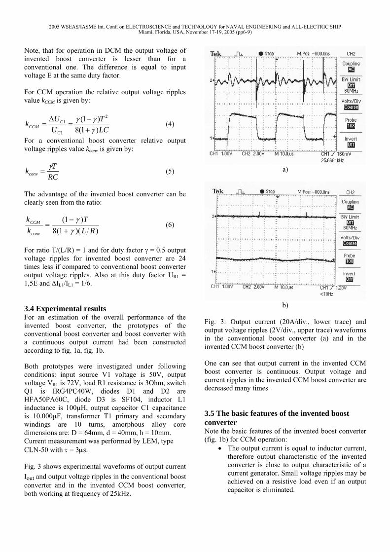
3.4 Experimental results For an estimation of the overall performance of the invented boost converter, the prototypes of the conventional boost converter and boost converter with a continuous output current had been constructed according to fig. 1a, fig. 1b. Both prototypes were investigated under following conditions: input source V1 voltage is 50V, output voltage VR1 is 72V, load R1 resistance is 3Ohm, switch Q1 is IRG4PC40W, diodes D1 and D2 are HFA50PA60C, diode D3 is SF104, inductor L1 inductance is 100µH, output capacitor C1 capacitance is 10.000µF, transformer T1 primary and secondary windings are 10 turns, amorphous alloy core dimensions are: D = 64mm, d = 40mm, h = 10mm. Current measurement was performed by LEM, type CLN-50 with τ = 3µs. Fig. 3 shows experimental waveforms of output current Iout and output voltage ripples in the conventional boost converter and in the invented CCM boost converter, both working at frequency of 25kHz.
a)
b)
Fig. 3: Output current (20A/div., lower trace) and output voltage ripples (2V/div., upper trace) waveforms in the conventional boost converter (a) and in the invented CCM boost converter (b) One can see that output current in the invented CCM boost converter is continuous. Output voltage and current ripples in the invented CCM boost converter are decreased many times. 3.5 The basic features of the invented boost converter Note the basic features of the invented boost converter (fig. 1b) for CCM operation:
• The output current is equal to inductor current, therefore output characteristic of the invented converter is close to output characteristic of a current generator. Small voltage ripples may be achieved on a resistive load even if an output capacitor is eliminated.
2005 WSEAS/IASME Int. Conf. on ELECTROSCIENCE and TECHNOLOGY for NAVAL ENGINEERING and ALL-ELECTRIC SHIPMiami, Florida, USA, November 17-19, 2005 (pp6-9)

• At switch Q1 OFF-ON transition a leakage inductance of the transformer T1 limits recovery current of a diode D1. As a result there is no switching loss in Q1 and D1.
• Peak current in L1, Q1, D1 are reduced by UR1/E times (practically up to 1.6 times) compared to conventional boost converter.
• Output voltage ripples are many times less than in the conventional boost converter.
• The absence of capacitors with high current capability in the circuit permits to extend output power up to megawatt range.
• The disadvantage is the increased voltage across power switch Q1 during OFF state if compared to conventional boost converter.
4 Field of the invention The application of the described CCM boost converter can be effective at any power level, when reduced ripples of the output voltage is a matter of concern, or output capacitor of a large value is undesirable. It can be especially effective for high power level application due to reduced peak and RMS values of current for all elements employed.
Motor
PWM inverter
Q3 Q4
Q7Q6Q5
Q2
.
a)
.
CCM boost converter
Q1
BT1
T1
D3
D2
L1
C1+
D1
..
b)
D1
D2
R1
T1
C1
+
Q1 D3
L1
BT1
.
c)
.
D4Q2
R1
D2
T1
D1L1
Q1
D3
BT1
Fig. 4: Invented CCM boost converter applications
Some applications of the CCM boost converter are shown in fig. 4: a - battery powered PWM inverter motor drive with overdrive option, b - battery output voltage stabilizer, c – step-up – step-down converter with continuous output current and output voltage from 0 to 1.6Vin for power management applications. 5 Conclusion Invented CCM boost converter prototype was developed and investigated, basic relationships for invented boost converter are derived, experimental results are presented. The invented boost converter provides a continuous output current for output voltage transformation up to 1.6 times. Output capacitor value may be reduced many times without increasing output voltage ripples across the load, if compared to conventional boost converter. The current value for an inductor, switch and diode is up to 1.6 times less in comparison with the conventional boost converter. Primary current consumption is 50% modulated. This advantages permit to recommend use of the invented CCM boost converter in marine and naval engineering. References
[1] A.J. Blokland, E. van Dijk, “Challenges and limitations of All Electric Ship designs”, Power electronics and applications EPE’2001, Graz, Austria, August 2001
[2] V.M. Borovikov, Yu.I. Krasnikov, “Boost converter”, Patent RU № 2241299 (International application № PCT/RU2004/000278).
2005 WSEAS/IASME Int. Conf. on ELECTROSCIENCE and TECHNOLOGY for NAVAL ENGINEERING and ALL-ELECTRIC SHIPMiami, Florida, USA, November 17-19, 2005 (pp6-9)