bonding in solids - louisiana tech universityupali/chem481/slides/chem245_structure of solids...1...
TRANSCRIPT

1
Section 4(M&T Chapter 7)
Structure and Structure and EnergeticsEnergetics of of
Metallic and Ionic SolidsMetallic and Ionic Solids
Bonding in Solids
• We have discussed bonding in molecules with three models:
– Lewis
– Valence Bond
– MO Theory
• These models not suitable for describing bonding in solids
(metals, ionic compounds)
• The structures of many solids (e.g. NaCl(s), Fe(s)) are best
described by a lattice model, in which atoms (ions) of the
lattice are placed in highly ordered arrangements (crystal
lattices)
• Arrangement yields maximum net attractive force with other
ions/atoms in the lattice and minimum repulsive forces
Close-Packing
• Treat the atoms of a metal (or ions of an ionic
substance) as spheres (e.g. marbles).
• Fill a tray until its surface is covered with a layer
of marbles, get a picture that looks something like
this:
• In this model, all spheres are touching the surface of six
other spheres (except those on the edges/corners) – a
hexagonal arrangement
• This arrangement is one layer of what is called a “close-
packed” arrangement
• See that there are also six spaces around each sphere
• If we were to pile another layer on top of this, it would
appear as follows…
Close-Packing
Around each sphere, there
are a total of six spaces Put next layer
of spheres into
three of them
Close-Packing
• So far, the levels are different (the spheres are not located inthe same space directly above the first level), so we have an “AB-type” arrangement for the two layers
• Note the spaces (hollows) that are now present – two types:
– “A” – located above a sphere
– “C” – located above a space
When the next closeWhen the next close--packed level is added, only threepacked level is added, only three
of the spaces surrounding each sphere can be occupiedof the spaces surrounding each sphere can be occupied
A
A AC
C
C

2
Close-Packing
If we were to add another closeIf we were to add another close--packed level on top, we could do so in two ways:packed level on top, we could do so in two ways:
Put 3rd layer
into A hollows
Put 3rd layer
into C hollows
AC
C CCA
Close-Packing
• In the upper figure (ABA-type) the top level was created
by putting spheres into the spaces labeled “A” of the
second layer
• The top level here is thus the same as the first (bottom)
level (the spheres in this level are located directly above
those of the first level) – an “ABAB…” arrangement
ABA arrangement
Close-Packing
•In the lower figure (ABC-type), the top layer was
constructed by placing spheres in the spaces labeled “C” of
the second layer
•This results in a level that is different than either of the
first two levels (an “ABC…” arrangement)
ABC arrangement
Close-Packed Arrangements
• These two arrangements shown below, are represented
as ball-and-stick arrangements, and not meant to imply
that spheres are not touching
• Which is which?The coordination number (CN)
in each of these lattices is 12.
Top layer different
than bottom
Close-Packed Arrangements• The unit cells are called:
a) hexagonal close-packed (hcp) – describing
an “ABABAB…” arrangement
b) cubic close-packed (ccp) – this describes an
“ABCABC…” ordering
hcp ccp
(this is also known as a “face-
centered cubic” arrangement)
Close-Packed Arrangements
• The unit cells are shown below as spherical models
– Cubic close-packed (ccp) (face-centered cubic)
– Hexagonal close-packed (hcp)
3
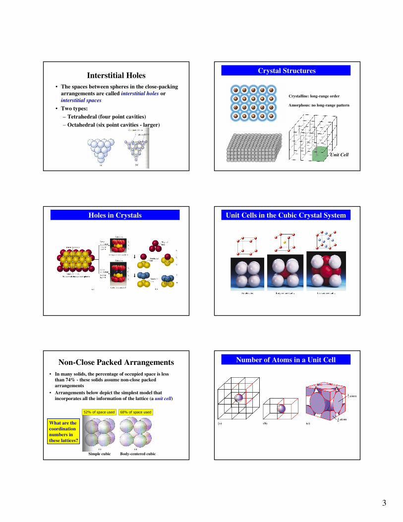
Interstitial Holes
• The spaces between spheres in the close-packing
arrangements are called interstitial holes or
interstitial spaces
• Two types:
– Tetrahedral (four point cavities)
– Octahedral (six point cavities - larger)
Crystal Structures
Amorphous: no long-range pattern
Crystalline: long-range order
Unit Cell
Holes in Crystals Unit Cells in the Cubic Crystal System
Non-Close Packed Arrangements
• In many solids, the percentage of occupied space is less
than 74% - these solids assume non-close packed
arrangements
• Arrangements below depict the simplest model that
incorporates all the information of the lattice (a unit cell)
What are the
coordination
numbers in
these lattices?
Simple cubic Body-centered cubic
52% of space used 68% of space used
Number of Atoms in a Unit Cell
Face centered unit cell
contains 8 corners @ 1/8 atom + 6 faces @ ½ atom = 4 atoms

4
Counting Cell Occupancy
2 atoms 4 atoms 1 atom
circle = bcc
diamond = hcp
+ = ccp (fcc)
Data quoted for T = 298 K
X-Ray Diffraction : Crystallography
Diffraction of X-Rays
Constructive interference of the x-rays only when the
pathlength in the crystal is a whole multiple of the wavelength
Bragg Equation: nλλλλ = 2d sin θθθθ, n = 1, 2, 3, …
Polymorphism
• The lattice structure adopted by an element may change
as the temperature and/or the pressure is changed
• A substance that can exist in more than one crystalline
form is said to be polymorphic
• Next slide – a phase diagram for Fe
• Phase diagram – lines (phase boundaries) separate
different phases of a substance
• On a line, have both phases present in equilibrium
5
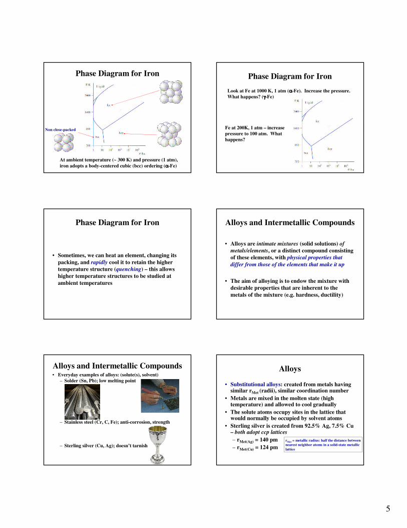
Phase Diagram for Iron
Non close-packed
At ambient temperature (~ 300 K) and pressure (1 atm),
iron adopts a body-centered cubic (bcc) ordering (αααα-Fe)
Phase Diagram for Iron
Look at Fe at 1000 K, 1 atm (αααα-Fe). Increase the pressure.
What happens? (γγγγ-Fe)
Fe at 200K, 1 atm – increase
pressure to 100 atm. What
happens?
Phase Diagram for Iron
• Sometimes, we can heat an element, changing its
packing, and rapidly cool it to retain the higher
temperature structure (quenching) – this allows
higher temperature structures to be studied at
ambient temperatures
Alloys and Intermetallic Compounds
• Alloys are intimate mixtures (solid solutions) of
metals/elements, or a distinct compound consisting
of these elements, with physical properties that
differ from those of the elements that make it up
• The aim of alloying is to endow the mixture with
desirable properties that are inherent to the
metals of the mixture (e.g. hardness, ductility)
Alloys and Intermetallic Compounds• Everyday examples of alloys: (solute(s), solvent)
– Solder (Sn, Pb); low melting point
– Stainless steel (Cr, C, Fe); anti-corrosion, strength
– Sterling silver (Cu, Ag); doesn’t tarnish
Alloys
• Substitutional alloys: created from metals having similar rMet (radii), similar coordination number
• Metals are mixed in the molten state (high temperature) and allowed to cool gradually
• The solute atoms occupy sites in the lattice that would normally be occupied by solvent atoms
• Sterling silver is created from 92.5% Ag, 7.5% Cu – both adopt ccp lattices
– rMet(Ag) = 140 pm
– rMet(Cu) = 124 pm
rMet = metallic radius: half the distance between
nearest neighbor atoms in a solid-state metallic
lattice

6
Substitutional Alloys Alloys
• Interstitial alloys: solute atoms occupy the
interstitial spaces (cavities) of a host lattice (e.g.
carbon steel)
– Low C steel: 0.03 – 0.25% C (steel sheeting)
– Medium C steel: 0.25 – 0.70% (bolts, screws, etc.)
– High C steel: 0.8 – 1.5% (cutting, drilling tools)
Intermetallic Compounds
• Some melts (combinations of metals in the molten
state) will solidify in arrays that are different than
either of the components that make up the mixture –
these compounds are called intermetallic
compounds
• Brass (Cu, Zn) is an intermetallic compound -
γγγγ-brass has a formula of Cu5Zn8
Alloys and Intermetallic Compounds
• Alloys are intimate mixtures (solid solutions) of
metals/elements, or a distinct compound consisting
of these elements, with physical properties that
differ from those of the elements that make it up
• The aim of alloying is to endow the mixture with
desirable properties that are inherent to the
metals of the mixture (e.g. hardness, ductility)
Diamond
• In diamond, C-atoms take
on a fcc-type arrangement
• Each C-atom is four-
coordinate (tetrahedral)
and so possesses a
complete octet of electrons
through covalent bonds
• Also adopted by Si, Ge, Sn
and Pb (other C-group
elements)
Graphite
• The most thermodynamically stable
form of carbon (diamond is
metastable), graphite consists of
layers of carbon sheets that are built
from fused, 6-membered carbon rings
• The bonding that exists within a layer
is covalent (and delocalized), but
between planes, dispersion forces
(non-covalent) hold the rings together
(weak intermolecular force)

7
Unit Cells• The smallest collection of spheres that describes a lattice
(when it is repeated) is the unit cell
• Some of the atoms in a unit cell are shared with other cells,
and so they do not belong entirely to one cell
Example, the atoms at the corners of the
cell shown on the right are shared with
seven other cells
Each contributes 1/8 of an atom to the
cell shown, and is called a “corner site”
Corner site
Face-centered site
A face-centered cubic unit cell
Unit Cell Contributions
• Corner sites each contribute 1/8 of a
sphere to a cell
• Edge sites contribute ¼ sphere to the
cell
• Face sites contribute ½ sphere to the cell
• Sites contained in the cell (e.g. the
center site of a bcc cell) contribute 1
each
Face-centered site
How many spheres (atoms/ions) occupy
- a simple cubic unit cell?
- a body-centered cubic cell?
- a face-centered cubic cell?
Ionic Solids
Particles: Cations (+) – small size
Anions (-) – large size
UNIT CELL dimensions usually determined by the
arrangement of the large ANIONS.
Cations fit into the “holes” within the anion structure
Holes in Crystals
(2R)2+(2R)2 = (2R+2r)2
••••
••••
r = 0.414R
Radius Ratios• A rough guide for predicting structures of salts
(cations and anions). Use rcation/ ranion, or r+/r-)
Value of r+/r-Predicted
Coordination
Number of
Cation
Predicted
Coordination
Geometry of
Cation
<0.15 2 Linear
0.15-0.22 3 Trigonal Planar
0.22-0.41 4 Tetrahedral
0.41-0.73 6 Octahedral
>0.73 8 Cubic
Sodium Chloride
rNa+/RCl- = 102 pm/ 181 pm = 0.56,
expect Na+ to occupy octahedral holes.

8
Holes in Crystals
Four types of holes:
trigonal < tetrahedral < octahedral < cubic
too small
for any
cation
Final arrangement depends on relative sizes of
cations and anions plus the required stoichiometryThis is an example of a binary solid (two elements involved) – what is its formula?
Dimensions of Cubic Lattices• For cubic unit cells, it is possible to determine cell lengths (edge) and
dimensions of lattice spaces
• For example, a simple cubic cell will have an edge length of 2r, where
r is the radius of a sphere
• It can be shown that the corner-to-corner length indicated in the
picture will be √√√√3××××a
Each sphere has a radius of r
Each edge length (length of the edge of the
unit cell) is then 2r (spheres in contact)
Can also be shown that
- a sphere of radius up to 0.73r can fit
in the center
-the atoms occupy 52% of the available
space of the unit cell
a
√√√√3××××a
Simple cubic unit cell
In this diagram, let a = 2r
√√√√2××××a
Rock Salt Lattice (NaCl)
• Interpenetrating fcc lattices of Na+ ions and Cl- ions (rem: fcc = ccp)
• Cl- ions are much larger then the Na+ ions (Cl-: 181 pm; Na+: 102 pm).
• Na+ ions are occupying octahedral holes in the unit cell shown
• Each Na+, Cl- ion is octahedral (six coordinate)
• NaCl-type lattice structures exist for many ionic compounds (NaF, NaBr, NaI, NaH, LiX, KX, RbX (X = halide), AgF, AgCl, AgBr, MgO, CaO, SrO, BaO, MnO, CoO, NiO, MgS, CaS, SrS, BaS)
Binary Lattices
CsCl Lattice
• Eight coordinate ions (cations and
anions) – body centered cubic
• Interpenetrating simple cubic-type
lattice
• Adopted by CsBr, CsI, TlCl, TlBr
CaF2 (Fluorite) Lattice• Eight-coordinate cations (Ca2+, grey spheres)
• Four-coordinate anions (F-, blue spheres)
• Six cations are face-positioned, shared between adjacent cells.
• This lattice type adopted for group II metal fluorides, BaCl2, and f-block metal dioxides
• Exchanging the cations and anions in this structure would yield an antifluorite lattice – M2X stoichiometry. Adopted by some group I metal oxides and sulfides (e.g. Na2S).

9
Zinc blende, ZnS (diamond type) lattice
• Similar to the fluorite lattice, with removal of half of the
anions (so MX2 to MX stoichiometry).
• Looks something like the structure shown for diamond –
each atom is in a tetrahedral environment
How many Zn, S
atoms exist in thisstructure?
Zn: grey
S: blue
Wurtzite (ZnS) lattice
• Wurtzite formed by high
temperature transition
from zinc blende
• Hexagonal prism unit cell
with all ions tetrahedrally
sited
• How many Zn2+, S2- ions
exist in this structure?
β-cristobalite (SiO2) lattice
• Again, much like diamond
structure, but with oxygen
ions between the
tetrahedral Si ions.
• Si-O-Si bond angle in
figure is 180o, while in
practice, it is found to be
147o (bonding in SiO2 is
not purely electrostatic).
In a pure ionic model, electrostatic attraction would be the only factor that
would be expected to hold an ionic lattice together
Rutile (TiO2) structure
• Oxygen ions (white) are
trigonal planar while
titanium centers (black)
are octahedral.
• Four oxygen ions are face-
oriented, while two are
contained in the cell
Perovskite (CaTiO3) lattice
• A double oxide (oxygen atoms are coordinated to both
Ca2+ and Ti4+)
• Ca2+ ion is at center of cube unit cell
• Ti4+ ions at corners of the cube (eight of these)
• O2- ions at each edge of the cube (twelve of these)
CdCl2, CdI2 Lattices
• Common for MX2 structures to crystallize in this structure
• Can observe the layers as ABAB (layered lattices)
• I- ions (gold) are arranged in a hcp format with the Cd2+ ions (white) occupying octahedral holes.
• In CdCl2, the arrangement is ccp
• Attractive forces that exist between these planes is weak (dispersion forces), and so fracture of a crystal of this kind usually produces cleavage planes
CdI2 lattice

10
Energy Changes in the Formation of Ionic Crystals
Na(s) + ½ Cl2(g) →→→→ NaCl(s)
∆∆∆∆Hreaction = ∆∆∆∆Hf(NaCl(s))
Energy Changes in the Formation of Ionic Crystals
Lattice Energy
Born-Fajans-Haber Cycle
sublimation
bond energy
ionization energy
electron affinity
(Ionic Bond Strength)
Lattice Energies
• We have already looked at bond dissociation
enthalpies (energy required to break bonds in
homonuclear and heteronuclear diatomics)
• Energy is also required to break apart ionic
lattices, due to the large amount of electrostatic
forces that exist between the ions in the lattice
• Coulombic forces (attractions, repulsions)
• Born forces (electron-electron, nucleus-nucleus)
Energy Between Two Point
Charges• Consider what happens if we bring two point charges
from an infinite separation to form an ion pair:
Mz+(g) + Xz-(g) MX(g)
• We can calculate the change in internal energy (∆∆∆∆U) as:
• Z-, Z+ are the charges of the ions in electron units
• e is the charge of an electron (1.602 x 10⁻¹⁹ C)
• εo is the permittivity of a vacuum (8.854 x 10⁻¹² C2/J.m)
• r0 is internuclear separation
=∆ −+
0
2
0 4 επe
r
ZZU
• Because oppositely charged ions are attracted to one
another, energy is released in this process
• Consider the attractions and repulsions that exist in a rock
salt lattice (between oppositely-charged and like-charged
ions)
=∆ −+
0
2
0 4 επe
r
ZZU

11
A Summary of Attractions and Repulsions
• The attractions experienced by the Na+ ion are summarized as follows:
• 6 Xz- ions, each at a distance d (the ions at the face sites)
• 12 Mz+ ions, each at a distance (√√√√2)d (the ions at the edge sites)
• 8 Xz- ions each at a distance (√√√√3)d (the ions at the corner sites)
• 6 Mz+ ions each at a distance of (√√√√4)d (imagine the next set of pink spheres in figure beyond the face gray spheres)
Madelung Constants
• We must factor these attractions and repulsions
into the expression:
• Convergent series, which yields a number for each
lattice type that is called the Madelung constant, M
( )
−
+
−=∆ +−++−+ ...
4
6
3
8
2
126
4
222
ZZZZZZd
eU
oπε
Madelung Constants
• If we sum the interactions (attractive and repulsive) between the ions of this lattice, we get a convergent term (for this lattice, the value converges to a value of ~1.7476). This valueis obtained regardless of the actual charges on the ions.
• Madelung constants (M) are unique for each coordination environment (i.e., for each type of crystal lattice).
=∆ −+
0
2
0 4 επe
r
ZMZU
Table 7-2, M. & T.
Lattice Energy (almost there…)
• The internal energy change for the formation of one mole of an ionic lattice in this arrangement is then calculated as:
• N = Avogadro’s number (6.022 x 10²³ mol-1)
• but what about Born forces? (nuclear-nuclear, electron-electron forces)
=∆ −+
0
2
0 4 επe
r
ZNMZU
Lattice Energies
• If we consider electrostatic and Born forces, we
arrive at the Born-Mayer equation (evaluated at
equilibrium internuclear separation, ro)
• ρρρρ corrects for repulsions at short distances.
Typically, a value of 30 pm is used for ρρρρ.
•Lattice energy can also be defined as the energy required to pull apart an ionic latticeinto its gas-phase ions, as defined in M&T, in which case, it is a positive energy
Correction for
Born forcesThis equationwill enable us
to predict latticeenergies (calledthe calculated
lattice energy
( )
−
=∆ −+
00
2
0
1 4
K 0r
e
r
ZNMZU
ρεπ
Lattice Energies
• Lattice energy can be defined as the internal energy change associated with the formation of one mole of the solid from its constituent gas phase ions at 0 (zero) Kelvin. Thus, at 0K, the lattice energy corresponds to the process:
Mn+(g) + nX-
(g) MXn(s)
Lattice energies may be estimated by assuming an electrostatic model (ions are point charges) – a good approximation in some cases. In others, not so good.

12
Sample Calculation: Lattice Energy
• Calculate the lattice energy for NaCl (rNa-Cl = 283 pm)
( )( )
molkJ
molJ
pm
pm
mmJC
CKU
/767
/766871
283
301
)10283)(10854.8(4
)10602.1(11)7476.1)(10022.6()0(
121.1.212
21923
−=
−=
−
××
×−+×=∆
−−−−
−
π
rNa+ = 116 pm
rCl- = 167 pmAppendix B
( )
−
=∆ −+
00
2
0
1 4
K 0r
e
r
ZNMZU
ρεπ
Lattice Energies
• We see there is only a minor discrepancy between the value
obtained with the Born-Mayer equation (-767 kJ/mol) and
the Born-Fajans-Haber thermodynamic cycle (-787 kJ/mol)
• For NaCl, there’s only a ~2% difference between the
calculated and experimental energies (an ionic model
provides a good approximation of NaCl)
Lattice Energies• Since the calculated values agree so well (2% error), we see the
electrostatic model is a reasonably good assumption for the type of
bonding which exists in a NaCl(s)
lattice
• Not true for layered structures like CdI2(s) – recall the forces that exist in
this structure
• We also see that for silver halides, the calculated and experimental
energies differ greatly, in the order AgF<AgCl<AgBr<AgI. The bonding
with larger halide ions has more covalent character, and thus an ionic
approximation does not hold
F Cl Br I
CHEM 245
Interactive 3-D Crystal Structures:
http://www.chemtube3d.com/solidstate/_table.htm
Radius Ratios
• These guidelines often yield incorrect predictions – example: LiBr(r+/r- = 0.38; tetrahedral)
• Predict only one coordination geometry for a given combination of ions (not helpful for polymorphic samples)
• Examples:
– What is the coordination number of Ti in rutile? (rTi3+ = 75 pm; rO2- = 124 pm)
– What is C.N. of Ca in fluorite? (rCa2+ = 126 pm; rF- = 117 pm)
– What is C.N. of Zn in zinc blende? (rZn2+ = 77pm; rS2- = 170 pm)
Electrical Conductivity in Metals,
Semiconductors, and Insulators
• Electrical conductivity is a property displayed by metals and some inorganic and organic materials
• Loosely defined as the ability of a substance to permit movement of electrons throughout its volume
• On a molecular level, electrons can be passed around (atom-to-atom) by being promoted into empty orbitals on otheratoms
• For solid structures a modification of Molecular Orbital Theory called Band Theory is used to explain conductivity

13
Electrical Conductivity and Resistivity
• Resistivity (ρρρρ) measures a substance’s electrical
resistance for a wire of uniform cross-section
• Resistance is measured in ohms (ΩΩΩΩ)
• Conductivity is 1/resistivity. Units of conductivity
are ΩΩΩΩ-1m-1 or S/m (S = Siemens; S = ΩΩΩΩ-1)
( )( )( )2/_sec
//
mareationalcross
mlengthmyresistivit
a
lR
−
Ω==
ρ
Electrical Conductivity and Resistivity
• The resistivity of a
metal increases
(conductivity
decreases) with
increasing
temperature
“electrical resistivity”Ωm
Electrical Conductivity and Resistivity
• The resistivity of a
semiconductor decreases
(conductivity increases) with
increasing temperature
Resistivity with temperature for a semiconductor
MO Theory Approach to Band Theory
• Consider a line of H-atoms that interact through their valence s-orbitals.
As more H-atoms interact, more MO’s are created
In the infinite structure, there is a continuum of energy states - a “band” (non-quantized)
Valence orbitals overlap to create a “valence band”
Band Theory of MetalsIn order for electrons to be able to move through a material, they must jump
from an occupied molecular orbital to an unoccupied orbital. In a metal, this
should be easily accomplished (metals are highly conductive).
Lithium (and other alkali metals) have a half-filled valence s-orbital (occupied).
In the infinite solid, there will be a half-full band. Electrons can move into an
unoccupied MO with minimal energy cost (small applied potential)
density of
states isgreatest
in themiddle of
the band
Band that is created from occupiedorbitals is called “valence band”
unoccupied orbitals produce
a “conduction band”
Band Theory of Metals• For the metal, Be (2s2), how does electron
movement occur? (valence band is full)
• The energy separation of 2s and 2p orbitals in Be is small enough that the conduction band (band that derives from unoccupied orbitals) overlaps the valence band
electron movement canelectron movement can
occur by an electron jumpingoccur by an electron jumping
from the valence band into anfrom the valence band into an
energyenergy--matched unoccupiedmatched unoccupied
conduction band orbitalconduction band orbital

14
Semiconductors and Band Gaps
• In many materials (e.g. diamond), there is an energy gap (band gap, Eg) between the valence band and the conduction band
• For C, the energy separation that exists between the 2s and 2p valence orbitals is not small enough for valence band-conduction band overlap to occur in the bulk material (e.g. diamond)
– Metals have either partially filled valence bands or overlapping valence and conduction bands (e.g. Na)
– Insulators have fully occupied valence bands that are separated from the conduction band by a significant energy gap (e.g. diamond)
– Semiconductors have fully occupied bands that are separated from the valence band by a small energy gap (e.g. Si)
Band Theory
overlapping valence
and conduction bands
conduction
conduction
valence valence
band gap
Semiconductors
• For semiconductors, thermal energy will enable
electrons to move into the empty conduction band,
creating “holes” in the valence band (orbitals that
were occupied by electrons). The mobile electrons
(and holes) give rise to electrical conductivity.
• Pure materials that are electrically conductive
called intrinsic semiconductors
Extrinsic Semiconductors
• Certain semiconductors exhibit enhancedelectrical conductivity when small quantities of another element are present in the semiconductor lattice (called doping).
• The band structure of silicon involves a band gap of approximately 106 kJ/mol (1.11 eV)
• Introduction of either gallium or arsenic in very small quantities creates an extrinsic semiconductor, with a band gap of only about 10 kJ/mol (0.10 eV)
Si adopts a diamond lattice
Semiconductors
s2 p2
Semiconductors
Ga
Ga

15
Band Theory
overlapping valence
and conduction bands
conduction
conduction
valence valence
band gap
n-Type Semiconductors
• Arsenic-doped silicon contains atoms having an additional valence electron (As is gr. 5A, Si Gr. 4A). As in a Si lattice use four of its electrons in bonding (one left over)
• Even a small number of As atoms in the Si matrix creates a “donor band” with an energy just below the energy of the Si conduction band (~10 kJ/mol below)
• Thermal energy can excite electrons from the donor band into the Si conduction band, yielding mobile charge carriers
The charge carriers in the Si band structure are electrons: “n-type” semiconductor
Si is n-doped by introducing P or As atoms
p-Type Semiconductors
• Ga has one less valence electron than Si
• Introduction of a small number of Ga
atoms (Gr. 3A) into the Si lattice
structure creates a hole (nothing for
silicon’s fourth electron to bond to)
• The energy of these holes creates a
band just above the valence band
energy (by ~ 10 kJ/mol), an “acceptor
band”
• Electrons can occupy this new band,
leaving holes in the Si valence band
The mobile holes in Si band structure yield conductivity The mobile holes in Si band structure yield conductivity –– a a ““pp--typetype”” semiconductorsemiconductor
Semiconductors
• Semiconductors can be inorganic or organic
• Inorganic semiconductors consist of main group elements
(Si, Ge, Ga, As, In,…)
• Organic semiconductors consist of conjugated carbon
structures, typically oligomers or polymers
**
n
* *n
S
* *n
N
* *n
H
N
* *n
Semiconductor Devices
• Thermal population of unoccupied states makes these
materials conductive; at 0 K, electrons occupy lowest
possible energies
p-type semiconductor at 0 K (left)
and at 298 K (right)
n-type semiconductor at 0 K (left)
and at 298 K (right)
The Fermi energy is energy at which an electron is
equally likely to be in occupied and unoccupied bands
Semiconductor Devices• The Fermi level serves to set the relative energies of the p-
type and n-type interfaces, and is the energy at which an e- is
equally likely to be in the valence or conduction band.
• In an intrinsic semiconductor, this lies in the middle of the
bandgap of the host semiconductor
• Doping:
– lowers the energy of the Fermi level to the region between
the acceptor band and the top of the host’s valence band
– raises the energy of the Fermi level to between the donor
band and the bottom edge of the host’s conduction band
intrinsic p-type n-type

16
Semiconductor Devices• When n- and p-type semiconductors
contact, mobile electrons in the n-type
layer near the interface can migrate
into the p-type layer, resulting in
recombination
• The extra electrons in the p-type layer
raise its energy and new holes in the n-
type layer lower its energy. Charge
movement ceases nearly immediately, as
the p-type layer accumulates negative
charge and the n-type layer positive
charge
• Recombination results in the formation
of a depletion zone at the junction. This
depletion zone is accompanied by its
own potential
p,np,n--junctionjunction
Diodes
When this kind of device is connected to a DC power source, a connection can be made in two ways:
1. Negative terminal to n-type layer, positive terminal to p-type layer (forward bias): as the potential at the negative terminal is made more negative (and the positive terminal more positive), the potential difference of the depletion zone can be overcome and a current flows (e-’srepelled by – terminal; holes repelled by + terminal)
-+ powersupply
Diodes
2. Negative terminal to p-type
layer; positive terminal to n-
type layer (reverse bias):
electrons and holes are pulled
away from the depletion zone.
Charge cannot move across
the junction and there is
essentially zero current
+- powersupply
Diodes
• Diodes are semiconductor devices
which permit current to flow in one
direction but not the other (current
rectifying), made through
combinations of p-type and n-type
semiconductors
• Such devices are useful in
electronics (e.g. in common
circuitry)
Photovoltaic Cells
• In the absence of an applied
potential, electrons can be made
to jump from valence to
conduction bands by absorbing
radiation (e.g. sunlight) and
through external connections,
can be used to power electronics
(solar calculators, solar panels)
Photoswitches
• Under reverse bias conditions, if the bandgap is small enough, visible radiation may be sufficient to promote electrons from the valence band to the conduction band (thus current flows in the presence of light – a photoswitch)
• Used in sensors (photodetectorsfor UV, visible, infrared radiation), automatic lights, etc.

17
Light Emitting Diodes (LEDs)
• Under forward bias conditions, electrons move from the n-
type layer (conduction band) into the p-type layer (valence
band)
• This movement results in recombination (releases energy).
When electrons fall into the holes of the p-doped layer, if the
energy change is of the right magnitude, visible light will be
emitted (luminescence)
• The color of the radiation emitted will depend on the
bandgap (Eg), so by varying the bandgap (by controlling the
composition of the semiconductor material), different colors
can be produced
Microscopic to Macroscopic
(Atomic Properties to Bulk Properties)
atoms, molecules
•discrete orbitals,
energy states
bulk solids
•bands, non-quantized
Quantum Dots
< 10 nmEnergy levels depend
strongly on size
Quantum Dots
Photoluminescence of
colloidal ZnSe Quantum Dots