board routability guidelines 1
TRANSCRIPT
R
1
2
3
4
A
B
C
D
escaped between two pads, assuming a space constraint equal to the trace width. For a discussion of signal routing specific to Virtex-II devices, see www.xilinx.com for currently available application notes.
As packages are able to handle more I/Os with a minimum increase in size, the signal integrity of those signals must be considered, regardless of clock frequency. Especially with the largest packages, precise PCB layer stackup is required. Parameters such as board material, trace width, pad type, and stackup must be defined based on simulation, and the fabrication drawings must be marked with “precise layer stackup” and the stackup specified. A number of board-level signal integrity simulators exist, and careful attention to PCB design rules creates a robust design with low EMI and high signal reliability.
Board Routability Guidelines
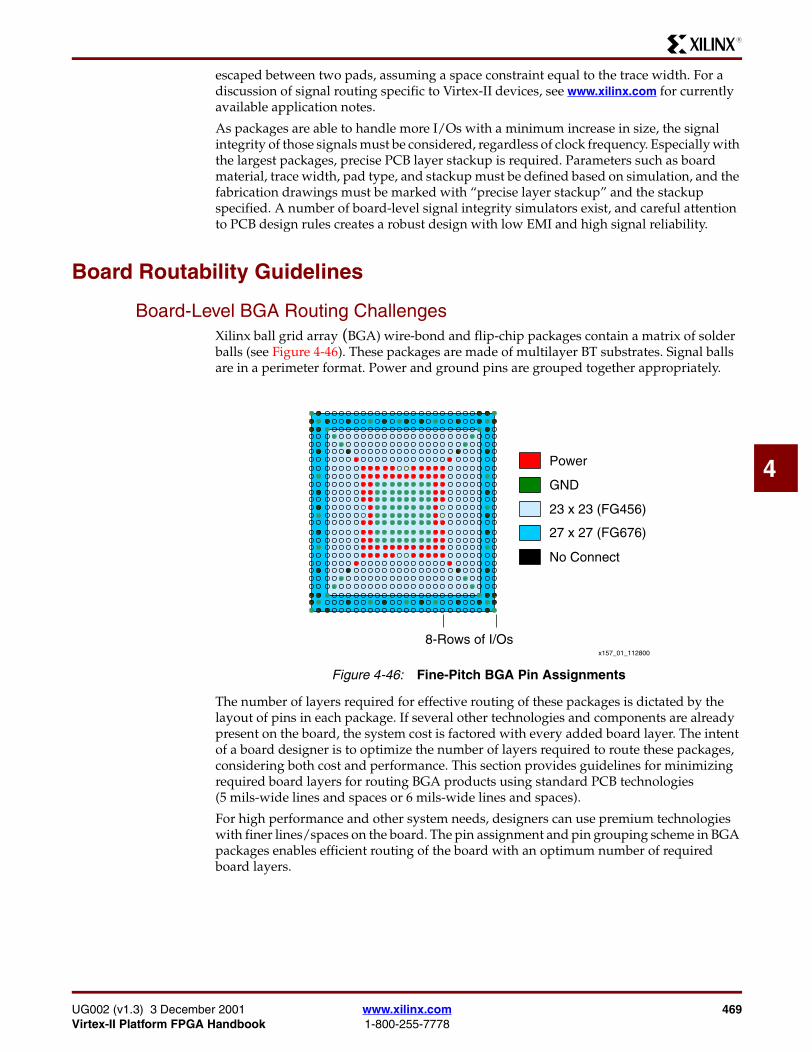
Board-Level BGA Routing ChallengesXilinx ball grid array (BGA) wire-bond and flip-chip packages contain a matrix of solder balls (see Figure 4-46). These packages are made of multilayer BT substrates. Signal balls are in a perimeter format. Power and ground pins are grouped together appropriately.
The number of layers required for effective routing of these packages is dictated by the layout of pins in each package. If several other technologies and components are already present on the board, the system cost is factored with every added board layer. The intent of a board designer is to optimize the number of layers required to route these packages, considering both cost and performance. This section provides guidelines for minimizing required board layers for routing BGA products using standard PCB technologies (5 mils-wide lines and spaces or 6 mils-wide lines and spaces).
For high performance and other system needs, designers can use premium technologies with finer lines/spaces on the board. The pin assignment and pin grouping scheme in BGA packages enables efficient routing of the board with an optimum number of required board layers.
Figure 4-46: Fine-Pitch BGA Pin Assignments
x157_01_112800
8-Rows of I/Os
27 x 27 (FG676)
23 x 23 (FG456)
Power
No Connect
GND
UG002 (v1.3) 3 December 2001 www.xilinx.com 469Virtex-II Platform FPGA Handbook 1-800-255-7778

R
Board Routing Strategy The diameter of a land pad on the component side is provided by Xilinx. This information is required prior to the start of board layout when designing the board pads to match component-side land geometry. Typical values for these land pads are described in Figure 4-47 and summarized in Table 4-5.
Figure 4-47: Suggested Board Layout of Soldered Pads for BGA Packages
x157_02_120500
Non-Solder-Mask-Defined Land Patterns orLand-Defined Land Patterns are recommended for all packages.
Mask Opening Outside of Land
VL
VH
e
D
W
M
L
Table 4-5: Summary of Typical Land Pad Values (mm)
Land Pad Characteristics CS144 FG256 FG456 FG676 BG575 BG728 FF896 FF1152 FF1517 BF957
Component Land Pad Diameter (SMD)4 0.35 0.45 0.45 0.45 0.61 0.61 0.58 0.58 0.58 0.61
Solder Land (L) Diameter 0.33 0.40 0.40 0.40 0.56 0.56 0.50 0.50 0.50 0.56
Opening in Solder Mask (M) Diameter 0.44 0.50 0.50 0.50 0.66 0.66 0.60 0.60 0.60 0.66
Solder (Ball) Land Pitch (e) 0.80 1.00 1.00 1.00 1.27 1.27 1.00 1.00 1.00 1.27
Line Width Between Via and Land (w) 0.130 0.130 0.130 0.130 0.203 0.203 0.130 0.130 0.130 0.203
Distance Between Via and Land (D) 0.56 0.70 0.70 0.70 0.90 0.90 0.70 0.70 0.70 0.90
Via Land (VL) Diameter 0.51 0.61 0.61 0.61 0.65 0.65 0.61 0.61 0.61 0.65
Through Hole (VH), Diameter 0.250 0.300 0.300 0.300 0.356 0.356 0.300 0.300 0.300 0.356
Pad Array - Full Full Full Full Full Full Full Full Full
Matrix or External Row 13 x 13 16 x 16 22 x 22 26 x 26 24 x 24 27 x 27 30 x 30 34 x 34 39 x 39 31 x 31
Periphery Rows 4 - 73 - - - - - - -
Notes: 1. Dimension in millimeters.2. 3 x 3 matrix for illustration only, one land pad shown with via connection.3. FG456 package has solder balls in the center in addition to the periphery rows of balls.4. Component land pad diameter refers to the pad opening on the component side (solder-mask defined).
470 www.xilinx.com UG002 (v1.3) 3 December 20011-800-255-7778 Virtex-II Platform FPGA Handbook

R
1
2
3
4
A
B
C
D
For Xilinx BGA packages, non-solder-mask defined (NSMD) pads on the board are suggested. This allows a clearance between the land metal (diameter L) and the solder mask opening (diameter M) as shown in Figure 4-47. The space between the NSMD pad and the solder mask, as well as the actual signal trace widths, depend on the capability of the PCB vendor. The cost of the PCB is higher when the line width and spaces are smaller.
Selection of pad types and sizes determines the available space between adjacent balls for signal escape. Based on PCB capability, the number of lines that can share the available space is described in Figure 4-48. Based on geometrical considerations, if one signal escapes between adjacent balls, then two signal rows can be routed on a single metal layer. This is illustrated in Figure 4-48 as routing with one line/channel, either at 6 mils-wide lines and spaces or 5 mils-wide lines and spaces. Using this suggested routing scheme, a minimum of eight PCB layers are required to route 10 signal rows in a package.
A slightly lower trace width can be used by the inner signal rows routed in internal layers than the width used in top and bottom external or exposed traces. Depending on the signal being handled, the practice of "necking down" a trace in the critical space between the BGA balls is allowable. Changes in width over very short distances can cause small impedance changes. Validate these issues with the board vendor and signal integrity engineers responsible for the design.
Figure 4-48 describes a board-level layout strategy for a Xilinx 1.0 mm pitch FG676 package. Detail A in Figure 4-48 describes the opening geometry for the Land Pad and the Solder Mask. Routing with 5 mils-wide lines or spaces allows one signal per channel (between the balls). For successful routing, eight-row deep signal traces require six PCB layers. Figure 4-49 shows the suggested schematic of layers for the six-layer routing scheme.
Figure 4-48: FG676 PC Board Layout/Land Pattern
x157_03_120500
1-Line/Channel5 mils Line/ 5 mils Spacing
(Standard Technology)
1-Line/Channel6 mils Line/ 6 mils Spacing
(Standard Technology)
O0.30 mm (0.012)
O0.61 mm (0.024)
O0.5 mm (0.020)
O0.4 mm (0.016) Detail "A"
I/O
GNDPWR
VCCINT
27 x 27 mm, 1.0 mm Fine Pitch BGA
PCB Design Rule (1.0 mm Ball Pitch)Lines PerChannel
PCBLayer
BallPad
ViaPad
1
TraceWidth/Spacing (mils)
5/5
I/ORows
8 6 .016" .024"
1.0 mm 1.0 mm
9.3 mils>5 mils
8.8 mils>5 mils
5 mils
6 mils
Detail "A"
Signal(L1)
Signal(L2)
Signal(L3)
Signal(L4)
PWRPlane
GNDPlane
1 mil = 0.0254 mm
UG002 (v1.3) 3 December 2001 www.xilinx.com 471Virtex-II Platform FPGA Handbook 1-800-255-7778

R
Using premium board technology, such as Microvia Technology (allowing up to 4 mils-wide lines and spaces), efficient routing is possible with a reduced number of board layers. A grouping scheme for power, ground, control, and I/O pins, might also enable efficient routing.
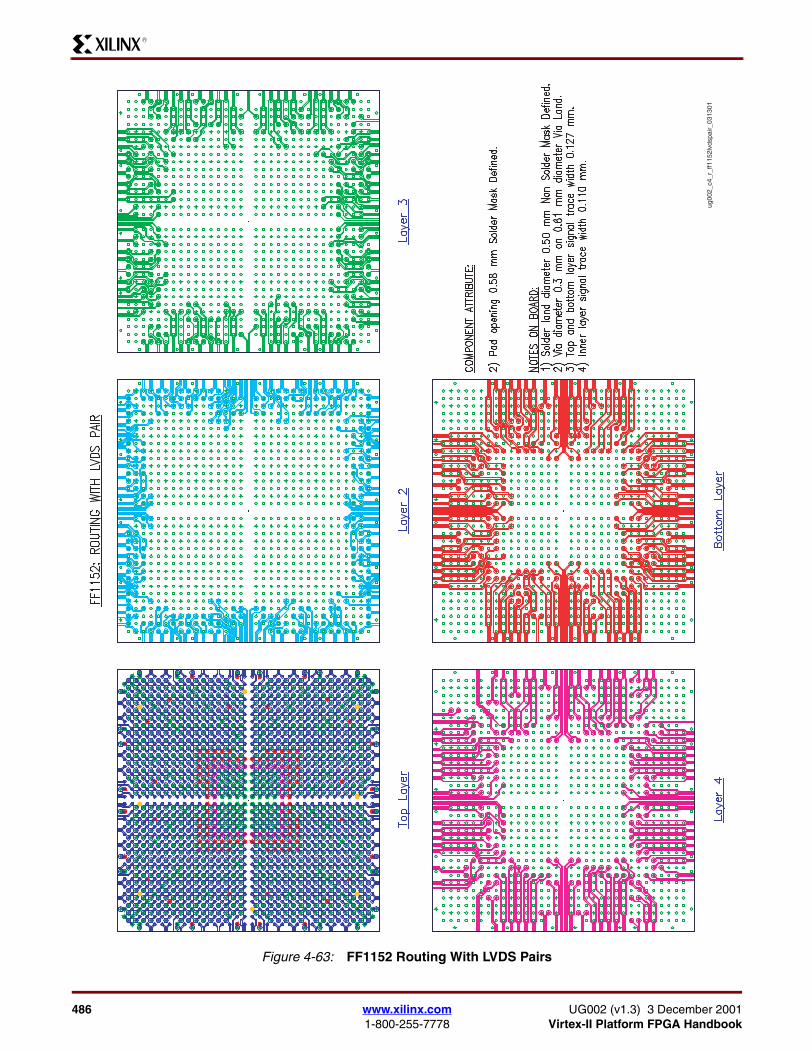
Figure 4-50 through Figure 4-67 show suggested layer-by-layer board routing for each Virtex-II package, including flip-chip packages. These drawings assume a standard PCB technology of 5 mils-wide lines and spaces. Table 4-6 lists the layer-by-layer routing examples provided. More details are contained in XAPP157, which is available on the web at www.xilinx.com/xapp/xapp157.pdf, as is a full-color (PDF) version of this document.
Figure 4-49: Six-Layer Routing Scheme
Table 4-6: Layer-By-Layer Board Routing Examples
Package Standard Routing Routing With LVDS Pairs
FG256 Top and bottom layers Top and bottom layers
FG456 Top, 2nd, and bottom layers Top, 2nd, and bottom layers
FG676 Top, 2nd, 3rd, and bottom layers Top, 2nd, 3rd, and bottom layers
BG575 Top, 2nd, and bottom layers Top, 2nd, and bottom layers
BG728 Top, 2nd, 3rd, and bottom layers Top, 2nd, 3rd, and bottom layers
FF896 Top, 2nd, 3rd, and bottom layers Top, 2nd, 3rd, and bottom layers
FF1152 Top, 2nd, 3rd, 4th, and bottom layers Top, 2nd, 3rd, 4th, and bottom layers
FF1517 Top, 2nd, 3rd, 4th, 5th, and bottom layers
Top, 2nd, 3rd, 4th, 5th, and bottom layers
BF957 Top, 2nd, 3rd, and bottom layers Top, 2nd, 3rd, and bottom layers
L - 2
L - 3
L - 4
L - 5
L - 6
L - 1Signal
Power/Gnd
Signal
Signal
Power/Gnd
Signalx157_04_051800
472 www.xilinx.com UG002 (v1.3) 3 December 20011-800-255-7778 Virtex-II Platform FPGA Handbook

R
1
2
3
4
A
B
C
D
Figure 4-50: FG256 Standard Routing
ug00
2_c4
_r_f
g256
_120
400
UG002 (v1.3) 3 December 2001 www.xilinx.com 473Virtex-II Platform FPGA Handbook 1-800-255-7778

R
Figure 4-51: FG256 Routing With LVDS Pairs
ug00
2_c4
_r_f
g256
lvds
pair_
1204
00
474 www.xilinx.com UG002 (v1.3) 3 December 20011-800-255-7778 Virtex-II Platform FPGA Handbook

R
1
2
3
4
A
B
C
D
Figure 4-52: FG456 Standard Routing
ug00
2_c4
_r_f
g456
_120
400
UG002 (v1.3) 3 December 2001 www.xilinx.com 475Virtex-II Platform FPGA Handbook 1-800-255-7778

R
Figure 4-53: FG456 Routing With LVDS Pairs
ug00
2_c4
_r_f
g456
lvds
pair_
1204
00
476 www.xilinx.com UG002 (v1.3) 3 December 20011-800-255-7778 Virtex-II Platform FPGA Handbook

R
1
2
3
4
A
B
C
D
Figure 4-54: FG676 Standard Routing
ug00
2_c4
_r_f
g676
_120
400
UG002 (v1.3) 3 December 2001 www.xilinx.com 477Virtex-II Platform FPGA Handbook 1-800-255-7778

R
Figure 4-55: FG676 Routing With LVDS Pairs
ug00
2_c4
_r_f
g676
lvds
pair_
1204
00
478 www.xilinx.com UG002 (v1.3) 3 December 20011-800-255-7778 Virtex-II Platform FPGA Handbook

R
1
2
3
4
A
B
C
D
Figure 4-56: BG575 Standard Routing
ug00
2_c4
_r_b
g575
_031
301
UG002 (v1.3) 3 December 2001 www.xilinx.com 479Virtex-II Platform FPGA Handbook 1-800-255-7778

R
Figure 4-57: BG575 Routing With LVDS Pairs
ug00
2_c4
_r_b
g575
lvds
pair_
0313
01
480 www.xilinx.com UG002 (v1.3) 3 December 20011-800-255-7778 Virtex-II Platform FPGA Handbook

R
1
2
3
4
A
B
C
D
Figure 4-58: BG728 Standard Routing
ug00
2_c4
_r_b
g728
_031
301
UG002 (v1.3) 3 December 2001 www.xilinx.com 481Virtex-II Platform FPGA Handbook 1-800-255-7778

R
Figure 4-59: BG728 Routing With LVDS Pairs
ug00
2_c4
_r_b
g728
lvds
pair_
0313
01
482 www.xilinx.com UG002 (v1.3) 3 December 20011-800-255-7778 Virtex-II Platform FPGA Handbook

R
1
2
3
4
A
B
C
D
Figure 4-60: FF896 Standard Routing
ug00
2_c4
_r_f
f896
_031
301
UG002 (v1.3) 3 December 2001 www.xilinx.com 483Virtex-II Platform FPGA Handbook 1-800-255-7778

R
Figure 4-61: FF896 Routing With LVDS Pairs
ug00
2_c4
_r_f
f896
lvds
pair_
0313
01
484 www.xilinx.com UG002 (v1.3) 3 December 20011-800-255-7778 Virtex-II Platform FPGA Handbook

R
1
2
3
4
A
B
C
D
Figure 4-62: FF1152 Standard Routing
ug00
2_c4
_r_f
f115
2_03
1301
UG002 (v1.3) 3 December 2001 www.xilinx.com 485Virtex-II Platform FPGA Handbook 1-800-255-7778
R
Figure 4-63: FF1152 Routing With LVDS Pairs
ug00
2_c4
_r_f
f115
2lvd
spai
r_03
1301
486 www.xilinx.com UG002 (v1.3) 3 December 20011-800-255-7778 Virtex-II Platform FPGA Handbook

R
1
2
3
4
A
B
C
D
Figure 4-64: FF1517 Standard Routing
ug00
2_c4
_r_f
f151
7_03
1301
UG002 (v1.3) 3 December 2001 www.xilinx.com 487Virtex-II Platform FPGA Handbook 1-800-255-7778

R
Figure 4-65: FF1517 Routing With LVDS Pairs
ug00
2_c4
_r_f
f151
7lvd
spai
r_03
1301
488 www.xilinx.com UG002 (v1.3) 3 December 20011-800-255-7778 Virtex-II Platform FPGA Handbook

R
1
2
3
4
A
B
C
D
Figure 4-66: BF957 Standard Routing
ug00
2_c4
_r_b
f957
_031
301
UG002 (v1.3) 3 December 2001 www.xilinx.com 489Virtex-II Platform FPGA Handbook 1-800-255-7778

R
Figure 4-67: BF957 Routing With LVDS Pairs
ug00
2_c4
_r_b
f957
lvds
pair_
0313
01
490 www.xilinx.com UG002 (v1.3) 3 December 20011-800-255-7778 Virtex-II Platform FPGA Handbook