bm70/71 data sheet - docs-apac.rs-online.com · the last character of the literature number is the...
TRANSCRIPT

BM70/71
Bluetooth® Low Energy (BLE) Module
Features
• Bluetooth SIG 4.2 qualified
• Certified to MIC and KCC radio regulations. FCC, IC, and NCC certifications are planned.
• European R&TTE Directive Assessed Radio Module is planned.
• UART, I2C, and SPI interface supported
• Supports transparent UART data service of BLE
• Built around Microchip IS187x SoC
• BM70 supports 3-channel PWM and BM71 sup-ports 1-channel PWM
• Precision Temperature Sensor (PTS) with operating range of -20°C ~ +70°C with an accuracy of +/- 3°C
• 12 bits Analog-to-Digital Converter (ADC) support for battery and voltage detection is provided. 8-channel ADC for BM70 and 5-channel ADC for BM71 is provided.
• 18 general purpose I/O pins (BM70) and 9 gen-eral purpose I/O pins (BM71)
• Integrated 32 MHZ crystal
• Small and compact surface mount module
• Castellated SMT pads for easy and reliable PCB mounting
RF Features
• ISM Band 2.402 GHz to 2.480 GHz operation
• Channels: 0-39
• Receive Sensitivity: typical -90 dBm (LE)
• Transmit Power: Class 2 output power (0 dBm typical, +2 dBm maximum)
• Received Signal Strength Indication (RSSI) monitor with 1db resolution
MAC/Baseband/Higher Layer Features
• Secure AES128 encryption
• GAP, GATT, SM, L2CAP and integrated public profile
• Create custom services using User Interface (UI) tool, a Windows® configuration utility
• I/O capability for BT4.0/BT4.2 authentication
• Software configurable role as peripheral/central, client/server
Antenna
• Integrated chip antenna (BM7xBLES1FC2)
• External antenna connection through RF pad (BM7xBLE01FC2)
Power Management
• Low-power modes supported, system wake-up through any GPIO
• Peak current: Tx 13 mA and Rx 13 mA with buck at 3.0V
Operating Conditions
• Operating voltage range: 1.9V to 3.6V
• Operating temperature: -20ºC to 70ºC
Note: The image is for representation purposeonly. The original product might differ inmarkings.
Note: This device has not been authorized asrequired by the rules of the Federal Com-munications Commission. This device isnot, and may not be, offered for sale orlease, or sold or leased, until authorizationis obtained.
2015 Microchip Technology Inc. Preliminary DS60001372C-Page 1

BM70/71
General Description
The BM70/71 module offers Bluetooth Low Energysolution for embedded applications. It conforms to theBluetooth core specification version 4.2 to enhance thethroughput and security for the IoT applications. It alsosupports Beacon technology to enhance user experi-ence for the IoT applications and enables users to con-trol the cloud and receive data without opening theapplication through a smart phone.
The BM70/71 integrated Bluetooth stack enablesdevelopers to focus the engineering resources on theapplication, instead of integrating Bluetooth connectiv-ity. The BM70/71 is available in different form factor tooptimize the space, cost, and RF performance. For por-table and wearable applications, it provides power-opti-mized design to minimize the current consumption toextend the battery life.
Applications
• Internet of Things (IoT)
• Payment/Security
• Wearable Devices
• Home and Security
• Health and Fitness
• Beacons
• Industrial and Data Logger
DS60001372C-Page 2 Preliminary 2015 Microchip Technology Inc.

BM70/71
Table of Contents
1.0 Device Overview .............................................................................................................................................................................. 52.0 Application information................................................................................................................................................................... 133.0 Module Configuration..................................................................................................................................................................... 254.0 Antenna.......................................................................................................................................................................................... 275.0 Electrical Characteristics................................................................................................................................................................ 356.0 Packaging Information ................................................................................................................................................................... 417.0 Soldering Recommendations ......................................................................................................................................................... 498.0 Ordering Guide .............................................................................................................................................................................. 51Appendix A: certification notices .......................................................................................................................................................... 53Appendix B: Revision History............................................................................................................................................................... 59
TO OUR VALUED CUSTOMERS
It is our intention to provide our valued customers with the best documentation possible to ensure successful use of your Microchipproducts. To this end, we will continue to improve our publications to better suit your needs. Our publications will be refined andenhanced as new volumes and updates are introduced.
If you have any questions or comments regarding this publication, please contact the Marketing Communications Department viaE-mail at [email protected] or fax the Reader Response Form in the back of this data sheet to (480) 792-4150. Wewelcome your feedback.
Most Current Data Sheet
To obtain the most up-to-date version of this data sheet, please register at our Worldwide Web site at:
http://www.microchip.com
You can determine the version of a data sheet by examining its literature number found on the bottom outside corner of any page.The last character of the literature number is the version number, (e.g., DS30000000A is version A of document DS30000000).
Errata
An errata sheet, describing minor operational differences from the data sheet and recommended workarounds, may exist for currentdevices. As device/documentation issues become known to us, we will publish an errata sheet. The errata will specify the revisionof silicon and revision of document to which it applies.
To determine if an errata sheet exists for a particular device, please check with one of the following:
• Microchip’s Worldwide Web site; http://www.microchip.com• Your local Microchip sales office (see last page)When contacting a sales office, please specify which device, revision of silicon and data sheet (include literature number) you areusing.
Customer Notification System
Register on our web site at www.microchip.com to receive the most current information on all of our products.
2015 Microchip Technology Inc. Preliminary DS60001372C-Page 3

BM70/71
NOTES:
DS60001372C-Page 4 Preliminary 2015 Microchip Technology Inc.

BM70/71
1.0 DEVICE OVERVIEW
The BM70/71 embedded 2.4 GHz Bluetooth version 4.2BLE module is built around Microchip TechnologyIS1870/71 BLE SoC (System on Chip). The IS1870/71SoC incorporates Bluetooth stack, power managementsubsystem, 2.4 GHz transceiver, and RF power ampli-fier. The user can embed Bluetooth functionality into anyapplications using the BM70/71 module.
The BM70/71 enables faster product development andtime to market. It is designed to provide simple Bluetoothsolutions with the following features:
• Simple integration and programming
• Reduced development time
• Superior wireless module with low-cost system
• Interoperability with Apple® iOS and Android™ OS
• Wide range of applications
In addition, the BM70/71 supports Beacon technologyto improve user experiences in IoT applications, suchas auto connection/control and data to cloud.
The BM70/71 can independently maintain a low- powerwireless connection, and the low-power usage and flex-ible power management maximizes the module’s lifetimein battery operated devices. Also, wide operating tem-perature range enables its use in indoor and outdoorenvironments.
The BM70/71 is a small, compact, surface mount on thehost PCB with the castellated pads making the interfaceeasy and reliable. The BM71 is relatively small form fac-tor module targeted for applications, such as wearablesports, fitness devices and so on.
1.1 Interface Description
Figure 1-1 and Figure 1-2 illustrate an example of theBM70/71 module-based system. Figure 1-3 throughFigure 1-6 details the pin diagrams. Table 1-1 providespin descriptions.
FIGURE 1-1: BM70-BASED SYSTEM BLOCK DIAGRAM
2015 Microchip Technology Inc. Preliminary DS60001372C-Page 5

BM70/71
FIGURE 1-2: BM71-BASED SYSTEM BLOCK DIAGRAM
DS60001372C-Page 6 Preliminary 2015 Microchip Technology Inc.

BM70/71
FIGURE 1-3: BM70BLE01FC2 PIN DIAGRAM
FIGURE 1-4: BM70BLES1FC2 PIN DIAGRAM
2015 Microchip Technology Inc. Preliminary DS60001372C-Page 7

BM70/71
FIGURE 1-5: BM71BLE01FC2 PIN DIAGRAM
FIGURE 1-6: BM71BLES1FC2 PIN DIAGRAM
DS60001372C-Page 8 Preliminary 2015 Microchip Technology Inc.

BM70/71
TABLE 1-1: PIN DESCRIPTION
BM70BLE01FC2
BM70BLES1FC2
BM71BLE01FC2
BM71BLES1FC2
Pin Name Type Description
— 1 — — GND Power Ground reference
— 2 — — GND Power Ground reference
1 3 12 13 GND Power Ground reference
2 4 11 14 VBAT Power Battery input. Voltage range: 1.9V to 3.6V
— — 10 — BK_IN Power Buck input. Voltage range: 1.9V to 3.6V
3 5 — — P2_2 DIO GPIO, default pull-high input PWM1
4 6 — — VDD_IO Power I/O positive supply. Do not connect. Ensure VDD_IO and MCU I/O voltage are compatible
5 7 — — VDD_IO Power I/O positive supply. Do not connect. Ensure VDD_IO and MCU I/O voltage are compatible
6 8 — — ULPC_O Power 1.2V programmable ULPC LDO output for AON-logic and retention memory sup-ply. Internal use only, do not connect to other devices.
7 9 — — P2_3 DI GPIO, default pull-high input PWM2
8 10 — — BK_O Power 1.55V buck output. internal use only, do not connect to other devices.
— — 13 6 P1_6 DIOAI
P1_6External 32.768 KHz crystal input: XI32K
— — 14 5 P1_7 DIOAO
P1_7External 32.768 KHz crystal output: XO32K
9 11 15 15 P2_7DIOAI
DODO
GPIO: P2_7ADC Input: AD14TX_INDSPI bus: NCS2, 2nd SPI bus (Master mode)
10 12 — — P1_1 DIOAIDI
GPIO: P1_1ADC Input: AD9SPI bus: MISO2, 2nd SPI bus (Master mode)
11 13 2 3 P1_2DIOAII/O
GPIO, default pull-high inputAD10I2C SCL
12 14 3 4 P1_3DIOAI
DIO
GPIO, default pull-high inputAD11I2C SDA
13 15 8 11 P0_0DIOAIDI
GPIO, default pull-high inputAD0UART flow-control CTS
14 16 — — P1_0 DIOAI
GPIO, default pull-high inputAD8
15 17 6 9 P3_6DIODODO
GPIO, default pull-high inputPWM0UART flow-control RTS
Legend: A = Analog D = Digital I = Input O = Output
2015 Microchip Technology Inc. Preliminary DS60001372C-Page 9

BM70/71
16 18 16 16 P2_0 DISystem configuration, default pull-high inputH: Application modeL: Test mode
17 19 — — P2_4 DIO GPIO, default pull-high input
18 20 — — NC — No connection
19 21 7 10 RST_N DI Module Reset (active-low) (internal pull-up)
20 22 5 7 HCI_RXD DI HCI UART data input
21 23 4 8 HCI_TXD DO HCI UART data output
22 24 — — P3_1 DIODO
GPIO: P3_1SPI bus: NCS, SPI Flash: CSN
23 25 — — P3_2 DIODO
GPIO: P3_2SPI bus: MISO, SPI Flash: SDO
24 26 — — P3_3 DIODI
GPIO: P3_3SPI bus: MOSI, SPI Flash: SDI
25 27 — — P3_4 DIODO
GPIO: P3_4SPI bus: SCLK, SPI Flash: SCK
26 28 — — P3_5 DIODO
GPIO, default pull-high inputLED1
27 29 — — P0_7 DIOAI
GPIO, default pull-high inputAD7
28 30 9 12 P0_2/LED DIOAI
P02AD2
29 31 17 2 GND Power Ground reference
— 32 — — GND Power Ground reference
30 — 1 1 BT_RF AI External antenna connection (50 Ω)
— 33 — — GND Power Ground reference
Legend: A = Analog D = Digital I = Input O = Output
BM70BLE01FC2
BM70BLES1FC2
BM71BLE01FC2
BM71BLES1FC2
Pin Name Type Description
DS60001372C-Page 10 Preliminary 2015 Microchip Technology
BM70/71
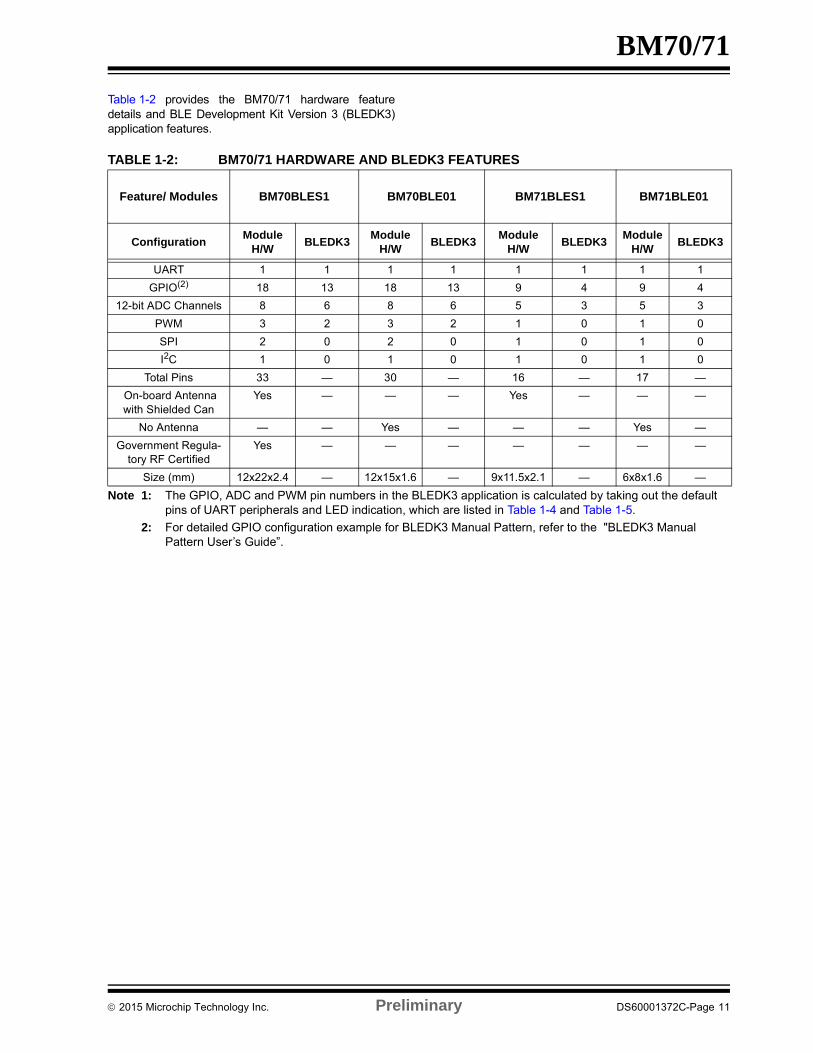
Table 1-2 provides the BM70/71 hardware featuredetails and BLE Development Kit Version 3 (BLEDK3)application features.TABLE 1-2: BM70/71 HARDWARE AND BLEDK3 FEATURES
Note 1: The GPIO, ADC and PWM pin numbers in the BLEDK3 application is calculated by taking out the default pins of UART peripherals and LED indication, which are listed in Table 1-4 and Table 1-5.
2: For detailed GPIO configuration example for BLEDK3 Manual Pattern, refer to the "BLEDK3 Manual Pattern User’s Guide”.
Feature/ Modules BM70BLES1 BM70BLE01 BM71BLES1 BM71BLE01
ConfigurationModule
H/WBLEDK3
Module H/W
BLEDK3 Module
H/WBLEDK3
Module H/W
BLEDK3
UART 1 1 1 1 1 1 1 1
GPIO(2) 18 13 18 13 9 4 9 4
12-bit ADC Channels 8 6 8 6 5 3 5 3
PWM 3 2 3 2 1 0 1 0
SPI 2 0 2 0 1 0 1 0
I2C 1 0 1 0 1 0 1 0
Total Pins 33 — 30 — 16 — 17 —
On-board Antenna with Shielded Can
Yes — — — Yes — — —
No Antenna — — Yes — — — Yes —
Government Regula-tory RF Certified
Yes — — — — — — —
Size (mm) 12x22x2.4 — 12x15x1.6 — 9x11.5x2.1 — 6x8x1.6 —
2015 Microchip Technology Inc. Preliminary DS60001372C-Page 11

BM70/71
Table 1-3 lists the details of the test pads used for theproduction test on the bottom of the BM70/71.Table 1-4 and Table 1-5 provide GPIO pin connectiondetails.TABLE 1-3: TEST PADS DETAILS
TABLE 1-4: BM70 GPIO CONFIGURATION
TABLE 1-5: BM71 GPIO CONFIGURATION
BM70BLE01FC2
BM70BLES1FC2
BM71BLE01FC2
BM71BLES1FC2
Pin Name Type Description
TP-1 TP-1 TP-3 TP-3 VCC_PA Power 1.55 V RF PA LDO
TP-2 TP-2 TP-1 TP-5 CLDO_O Power 1.2 V CLDO output
TP-3 TP-3 TP-2 TP-2 VCC_RF Power 1.2 V RF LDO output
— — TP-4 TP-4 ULPC_O Power 1.2 V ULPC LDO output
— — TP-5 TP-1 BK_O Power 1.55 V buck output
GPIO Pins Connection details
P2_0 System Configuration
P0_2 LED0
P0_0 UART_CTS
P2_7 UART_RX_IND
P3_6 UART_RTS
GPIO Pins Connection details
P2_0 System Configuration
P0_2 LED0
P0_0 UART_CTS
P2_7 UART_RX_IND
P3_6 UART_RTS
DS60001372C-Page 12 Preliminary 2015 Microchip Technology

BM70/71
2.0 APPLICATION INFORMATION
2.1 Reference Schematics
Figure 2-1 through Figure 2-4 illustrate the BM70/71reference circuits for various Stock Keeping Units(SKUs). The GPIOs are configurable and the connec-tion depends on the user’s application circuit.
The power input range is 1.9V~3.6V. If battery is used,the battery reverse protection circuit is recommended.The VDD_IO voltage is same as power input. If LED isused, ensure that the voltage is more than 3V to drivethe LED. It is recommended to implement the RFantenna matching circuit as shown in Figure 2-2 andFigure 2-3 to fine tune the antenna impedancematching.
FIGURE 2-1: BM70BLES1FC2 REFERENCE CIRCUIT
2015 Microchip Technology Inc. Preliminary DS60001372C-Page 13

BM70/71
FIGURE 2-2: BM70BLE01FC2 REFERENCE CIRCUIT
DS60001372C-Page 14 Preliminary 2015 Microchip Technology Inc.

BM70/71
FIGURE 2-3: BM71BLE01FC2 REFERENCE CIRCUIT
2015 Microchip Technology Inc. Preliminary DS60001372C-Page 15
BM70/71
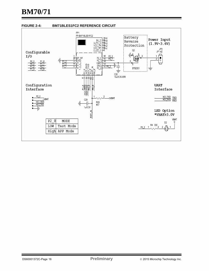
FIGURE 2-4: BM71BLES1FC2 REFERENCE CIRCUIT
DS60001372C-Page 16 Preliminary 2015 Microchip Technology Inc.

BM70/71
2.2 External Configuration and Programming
The BM70/71 can be configured and programmedusing an external configuration and programming tool.Figure 2-5 illustrates the test points that must beincluded on the host PCB for the development.
Configuration and programming modes can be enteredaccording to the system configuration I/O pins. Foradditional information, refer to Section 3.4 “SystemConfiguration”.
FIGURE 2-5: EXTERNAL CONFIGURATION AND PROGRAMMING
2015 Microchip Technology Inc. Preliminary DS60001372C-Page 17

BM70/71
2.3 Host MCU Interface
2.3.1 HOST MCU INTERFACE OVER UART
Figure 2-6 and Figure 2-7 illustrate the BM70/71 tohost MCU interface over UART. The Host Control Inter-face (HCI) UART lines are used to communicate
between the BM70/71 and MCU. The interface alsoillustrates the power scheme using a 3.3V Low-DropOut (LDO) regulator that supply 3.3V to the BM70/71(BAT_IN) and MCU VDD. This power scheme ensuresthat the BM70/71 and MCU I/O voltages are compati-ble.
FIGURE 2-6: BM70 TO MCU INTERFACE
Note 1: Ensure VDD_IO and MCU VDD voltages are compatible.
2: Control and indication ports are configurable.
DS60001372C-Page 18 Preliminary 2015 Microchip Technology Inc.

BM70/71
FIGURE 2-7: BM71 TO MCU INTERFACE
Note 1: Ensure VDD_IO and MCU VDD voltages are compatible.
2: Control and indication ports are configurable.
3: 10 uF (X5R) and 330 resistor are required for the BM71 module.
4: BK_IN connect to VBAT for BM71BLE01FC2.
2015 Microchip Technology Inc. Preliminary DS60001372C-Page 19

BM70/71
2.3.2 UART READY AFTER EXTERNAL RESET
In MCU applications, the time betweenReset/power-on and the BM70/71 UART port readmust be notified. Figure 2-8 illustrates the timing of theBM70/71 UART port ready for Test mode and Applica-tion mode after Reset.
FIGURE 2-8: TIMING DIAGRAM OF BM70/71 UART READY FOR TEST MODE AFTER RESET
DS60001372C-Page 20 Preliminary 2015 Microchip Technology Inc.

BM70/71
2.3.3 UART READY AFTER POWER-ON RESET
Figure 2-9 illustrates the timing of the BM70/71 UARTport ready for Test mode and Application mode afterPower-on Reset (POR).
In Application mode, when the BM70/71 is ready tocommunicate with the host MCU after Reset, theBM70/71 will have either Standby mode which is indi-
cated by the status pin, or a status report UART com-mand which is sent to inform the MCU that theBM70/71 is ready for communication.
FIGURE 2-9: TIMING DIAGRAM OF BM70 UART READY FOR TEST MODE AFTER POWER ON
2015 Microchip Technology Inc. Preliminary DS60001372C-Page 21

BM70/71
2.4 Standalone Configuration
Figure 2-10 illustrates the standalone configuration forthe BM71BLE01FC2 module. It also illustrates anapplication using a coin cell battery at VBAT input. For
the BM71, a 10 uF capacitor (X5R/X7R) is applied tothe BAT_IN pin. The BK_IN pin of the BM71BLE01FC2module must be connected to the BAT_IN pin.
FIGURE 2-10: BM71 STANDALONE CONFIGURATION
Note 1: Application includes ADC, PWM(BM70), I2C, and SPI bus interface.
DS60001372C-Page 22 Preliminary 2015 Microchip Technology Inc.

BM70/71
2.5 Power-Drop Protection
To prevent the BM70/71 from disruptions, when volt-age drops to less than 1.9V, an ‘Open Drain’ Reset chipwith delay time ≦ 10 ms that triggers Reset at 1.8V out-put voltage is recommended. Figure 2-11 illustrates theReset circuit block diagram.
FIGURE 2-11: RESET CIRCUIT BLOCK DIAGRAM
2015 Microchip Technology Inc. Preliminary DS60001372C-Page 23

BM70/71
NOTES:
DS60001372C-Page 24 Preliminary 2015 Microchip Technology Inc.
BM70/71
3.0 MODULE CONFIGURATION
The BM70/71 features and services can be configuredusing the Windows UI Configuration tool. For additionalinformation, refer to the “Windows UI Configuration toolUser Guide”.
3.1 UART Interface
The BM70/71 UART pins, TXD and RXD, are con-nected to the UART pins of the host MCU. It is recom-mended to use hardware flow control pins, RTS andCTS. By default, the BM70/71 hardware flow control isdisabled, and users must configure the pin to enablethe same. The UART baud rate is configurable.
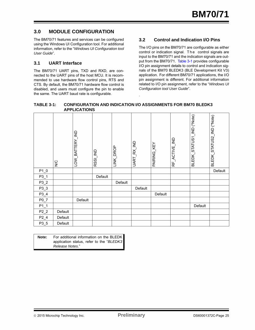
3.2 Control and Indication I/O Pins
The I/O pins on the BM70/71 are configurable as eithercontrol or indication signal. T h e control signals areinput to the BM70/71 and the indication signals are out-put from the BM70/71. Table 3-1 provides configurableI/O pin assignment details to control and indication sig-nals of the BM70 BLEDK3 (BLE Development Kit V3)application. For different BM70/71 applications, the I/Opin assignment is different. For additional informationrelated to I/O pin assignment, refer to the “Windows UIConfiguration tool User Guide”.
.
TABLE 3-1: CONFIGURATION AND INDICATION I/O ASSIGNMENTS FOR BM70 BLEDK3 APPLICATIONS
N/C
LOW
_B
AT
TE
RY
_IN
D
RS
SI_
IND
LIN
K_
DR
OP
UA
RT
_RX
_IN
D
PA
IRIN
G_
KE
Y
RF
_AC
TIV
E_I
ND
BLE
DK
_STA
TU
S1_
IND
(*N
ote)
BLE
DK
_STA
TU
S2
_IN
D (
*Not
e)
P1_0 Default
P3_1 Default
P3_2 Default
P3_3 Default
P3_4 Default
P0_7 Default
P1_1 Default
P2_2 Default
P2_4 Default
P3_5 Default
Note: For additional information on the BLEDKapplication status, refer to the “BLEDK3Release Notes.”
2015 Microchip Technology Inc. Preliminary DS60001372C-Page 25

BM70/71
Table 3-2 provides pin assignment details for the BM70BLEDK3 application.
TABLE 3-2: PIN ASSIGNMENT FOR BM70 BLEDK3 APPLICATION
3.3 Reset (RST_N)
The Reset input pin (RST_N) is used to Reset theBM70/71 with an active-low pulse with a minimum pulsewidth of 63 ns.
3.4 System Configuration
The P2_0 pin places the BM70/71 into operation modesas shown in Table 3-3. The P2_0 pin has an internalpull-up.
TABLE 3-3: SYSTEM CONFIGURATION SETTINGS
Pin Name Pin Assignment
P3_6 UART_RTS
P0_0 UART_CTS
P2_7 TX_IND
P1_2 I2C_SCL
P1_3 I2C_SDA
P0_2 LED0
P2_0 Operational Mode
High Application mode
Low Test mode (Write UI/Flash: Firmware Programming)
DS60001372C-Page 26 Preliminary 2015 Microchip Technology Inc.

BM70/71
4.0 ANTENNA
4.1 Antenna Characteristics
4.1.1 BM70BLES1FC2 CERAMIC CHIP ANTENNA
The BM70BLES1FC2 module contains an integralceramic chip antenna. The Figure 4-1 illustrates theantenna performance of the BM70BLES1FC2.
Table 4-1 provides the BM70BLES1FC2 moduleantenna characteristics.
FIGURE 4-1: BM70BLES1FC2 ANTENNA RADIATION PATTERN
TABLE 4-1: BM70BLES1FC2 ANTENNA CHARACTERISTICS
Parameter Values
Frequency 2442 MHz
Peak Gain 4.7 dBi
Efficiency 56.9%
2015 Microchip Technology Inc. Preliminary DS60001372C-Page 27

BM70/71
4.1.2 BM71BLES1FC2 CERAMIC CHIP ANTENNA
The BM71BLES1FC2 module contains an integralceramic chip antenna. The Figure 4-2 illustrates theantenna performance of the BM71BLES1FC2 module.
Table 4-2 provides the BM71BLES1FC2 antenna char-acteristics.
FIGURE 4-2: BM71BLES1FC2 ANTENNA RADIATION PATTERN
TABLE 4-2: BM71BLES1FC2 ANTENNA CHARACTERISTICS
Parameter Values
Frequency 2442 MHz
Peak Gain 0.1 dBi
Efficiency 42.7%
DS60001372C-Page 28 Preliminary 2015 Microchip Technology Inc.

BM70/71
4.2 Antenna Placement
For a Bluetooth wireless product, antenna placementaffects the whole system performance. The antennaneeds free space to transmit RF signals and cannot be
surrounded by the GND plane. Figure 4-3 andFigure 4-4 illustrate a typical example of the antennaplacement on the main application board with groundplane.
FIGURE 4-3: BM70BLES1FC2 ANTENNA PLACEMENT RECOMMENDATION
2015 Microchip Technology Inc. Preliminary DS60001372C-Page 29

BM70/71
FIGURE 4-4: BM71BLES1FC2 ANTENNA PLACEMENT RECOMMENDATION
DS60001372C-Page 30 Preliminary 2015 Microchip Technology Inc.

BM70/71
4.3 Host PCB Mounting Suggestion
4.3.1 BM70BLES1FC2 HOST PCB MOUNTING
Figure 4-5 illustrates the host PCB mounting sugges-tions for the BM70BLES1FC2 module, and it showsminimum ground plane area to the left and right of themodule for best antenna performance.
While designing the host PCB, the area under theantenna should not contain any top, inner, or bottomcopper layer. A low-impedance ground plane ensuresthe best radio performance (best range, low noise).The ground plane can be extended beyond the mini-mum recommended as required for the host PCB EMCnoise reduction. For best range performance, keep allexternal metal away by minimum 30 mm from theceramic chip antenna.
FIGURE 4-5: BM70BLES1FC2 HOST PCB MOUNTING SUGGESTION
2015 Microchip Technology Inc. Preliminary DS60001372C-Page 31

BM70/71
4.3.2 BM70BLE01FC2 HOST PCB MOUNTING
Figure 4-6 illustrates the mounting suggestions for theBM70BLE01FC2 module and it also shows a connec-tion to UFL connector. A low-impedance ground planewill ensure the best radio performance (best range, lownoise).
The pin_30 (BT_RF) is connected to an externalantenna connector, a PCB trace antenna, or a compo-nent (ceramic chip) antenna through a host PCB 50Ω
micro-strip trace. The micro-strip trace can beextended to include passive parts for antenna attenua-tion padding, impedance matching, or to provide testpoints. It is recommended that the micro-strip trace beas short as possible for minimum loss and best imped-ance matching. If the micro-strip trace is longer, itshould be a 50Ω controlled impedance.
FIGURE 4-6: BM70BLE01FC2 HOST PCB MOUNTING SUGGESTIONS
DS60001372C-Page 32 Preliminary 2015 Microchip Technology Inc.

BM70/71
4.3.3 BM71BLES1FC2 HOST PCB MOUNTING
Figure 4-7 illustrates the mounting suggestions for theBM71BLES1FC2 module. It also shows the areaaround the antenna required for the best antenna per-formance.
The area under the antenna should not contain any top,inner, or bottom copper layer when designing the hostPCB. A low-impedance ground plane ensures the bestradio performance (best range, low noise). The groundplane can be extended beyond the minimum recom-mended as required for the host PCB EMC noisereduction. For best range performance, keep all exter-nal metal away by minimum 30 mm from the ceramicchip antenna.
FIGURE 4-7: BM71BLES1FC2 HOST MOUNTING SUGGESTION
2015 Microchip Technology Inc. Preliminary DS60001372C-Page 33

BM70/71
4.3.4 BM71BLE01FC2 HOST PCB MOUNTING
Figure 4-8 illustrates the mounting suggestions for theBM71BLE01FC2 module. It also shows a connection tothe UFL connector. A low-impedance ground plane willensure the best radio performance (best range, lownoise).
The pin_1 (BT_RF) is connected to an externalantenna connector, a PCB trace antenna, or a compo-nent (ceramic chip) antenna through a host PCB 50Ωmicro-strip trace. The micro-strip trace can beextended to include passive parts for antenna attenua-tion padding, impedance matching, or to provide testposts. It is recommended that the micro-strip trace beas short as possible for minimum loss and best imped-ance matching. If the micro-strip trace is longer, itshould be 50Ω controlled impedance.
FIGURE 4-8: BM71BLE01FC2 HOST PCB MOUNTING SUGGESTION
DS60001372C-Page 34 Preliminary 2015 Microchip Technology Inc.

BM70/71
5.0 ELECTRICAL CHARACTERISTICS
This section provides an overview of the BM70/71 modules electrical characteristics. Additional information will beprovided in future revisions of this document.
Absolute maximum ratings for the BM70/71 devices are listed here. Exposure to the maximum rating conditions forextended periods may affect device reliability. Functional operation of the device at these or any other conditions, abovethe parameters indicated in the operation listings of this specification, is not implied.
5.1 Absolute Maximum Ratings
(See Note 1)
Ambient temperature under bias.............................................................................................................. .-20°C to +70°C
Storage temperature .............................................................................................................................. -65°C to +150°C
Voltage on VDD with respect to VSS ......................................................................................................... -0.3V to +3.6V
Maximum output current sunk by any I/O pin..........................................................................................................12 mA
Maximum output current sourced by any I/O pin ....................................................................................................12 mA
Note 1: Stresses above those listed under “Absolute Maximum Ratings” may cause permanent damage to thedevice. This is a stress rating only and functional operation of the device at those or any other conditions,above those indicated in the operation listings of this specification, is not implied. Exposure to maximumrating conditions for extended periods may affect device reliability.
2015 Microchip Technology Inc. Preliminary DS60001372C-Page 35

BM70/71
TABLE 5-1: ABSOLUTE MAXIMUM RATING
TABLE 5-2: RECOMMENDED OPERATING CONDITIONS
Symbol Condition Min. Max. UNIT
Supply voltage (VDD) — -0.3 3.6 V
Voltage on any digital pin — -0.3 VDD + 0.3 ≤ 3.9 V
Storage temperature range — -40 125 °C
Symbol Min. Typ. Max.
Ambient operating temperature range –20°C +25°C +70°C
PMU
VDD(VBAT, BK_IN), AVDD 1.9V 3.0V 3.6V
RST_N 1.9V 3.0V 3.6V
Other I/Os 1.9V — 3.6V
GPIO
VIH (Input High Voltage) 0.7 VDD — VDD
VIL (Input Low Voltage) VSS — 0.3VDD
VOH (Output High Voltage) (High drive, 12mA) 0.8 VDD — VDD
VOL (Output Low Voltage) (High drive, 12mA) VSS — 0.2VDD
Pull-up Resistance 34K 48K 74K
Pull-down Resistance 29K 47K 86K
Supply Current
TX mode peak current at VDD=3V, TX=0dBm, Buck mode
— — 13 mA
RX mode peak current at VDD=3V, Buck mode — — 13 mA
Link static current 60uA
Standby current 1.9 uA — 2.9 uA
Power-Saving 1 uA — 1.7 uA
Analog to Digital Converter (ADC)
Full scale (BAT_IN) 0V 3.0V 3.6V
Full scale (AD0~AD15) 0V — 3.6V
Conversion time (ENOB 8bit) — 131uS —
Conversion time (ENOB 10bit) — 387uS —
Operating current — — 500 uA
DNL -1.12LSB — +1.12 LSB
INL -4.38LSB — +4.38 LSB
Precise Temperature Sensor (PTS)
Detect range -20°C — 70°C
Digital Output 1387 — 2448
Resolution — 12 bits/°C —
Accuracy -3°C — +3°C
Conversion time (ENOB 10bit) — 12.35mS —
Operating current — — 200 uA
DS60001372C-Page 36 Preliminary 2015 Microchip Technology Inc.

BM70/71
5.2 Current Consumption Details
5.2.1 Tx/Rx MODE PEAK CURRENT CONSUMPTION DETAILS
Figure 5-1 and Figure 5-2 illustrate the Tx/Rx modepeak current consumption in connected mode. Thepeak current of the VBAT input is 13 mA in both themodes.
.
FIGURE 5-1: CURRENT CONSUMPTION IN Tx MODE
2015 Microchip Technology Inc. Preliminary DS60001372C-Page 37

BM70/71
FIGURE 5-2: CURRENT CONSUMPTION IN Rx MODE
For additional information on the current consumptionmeasurements, test conditions, and test environmentsetups, refer to the “BM70 and BLEDK3 ApplicationNote”. This Application Note covers the detailed infor-mation about the Tx/Rx data transfer in Connected
mode and four basic modes of BLE devices. Table 5-3details the status of the BLEDK3 application anddescription of each mode.
TABLE 5-3: STATUS OF BLEDK3 APPLICATION EXAMPLE
Note 1: CCCD stands for Client Characteristic Configuration in the GATT service characteristics.
Status Description
Shutdown Mode BLEDK3 is shutdown.
Standby Mode BLEDK3 sends advertising packets and wait for connection. BLEDK3 is discoverable and connectible.
BLE Connected Mode BLE link is established and CCCD of ISSC_Transparent_TX characteristic is disabled (see Note 1).
Transparent Service Enabled Mode BLE link is established and CCCD of ISSC_Transparent_TX characteristic is enabled (see Note 1).
DS60001372C-Page 38 Preliminary 2015 Microchip Technology Inc.

BM70/71
Note 1: Test condition: VBAT=3.3V, LED set off and measured in VBAT input.
2: Flash Code Version: BLEDK3 V1.03, UI Version:IS187x_102_BLEDK3_UIv100.123
3: Test Phone: iPhone® 6+ with iOS 9.02
4: Test Application Version: BLEDK3 V1.2
5: UI set flow control and RX_IND
6: For information on how to measure the current, refer to the “BM70 BLEDK3 Application Note”.
TABLE 5-4: BM70BLE01FC2 APPLICATION MODE CURRENT CONSUMPTION(1,2,3,4,5,6)
Test Mode/Test ConditionAverage Current
ConsumptionNote
Standby Mode Advertising Interval: 100 ms 0.23 mA UI: Set as beacon
Advertising Interval: 500 ms 0.077 mA UI: Set as beacon
BLE Connected Mode (no data exchange)
Connection Interval: 500 msSlave Latency: 2
0.08 mA Measured when transparent page is open on the BLEDK3 Applica-tion.
Transparent Service Enable ModeTx data
Connection Interval: 18.75 msSlave Latency: 0
3.87 mA Max Tx data throughput settingTested File size: 100 KBTx data throughput: 9.863 KB/s
Transparent Service Enable ModeTx data
Connection Interval: 40 msSlave Latency: 0
2.77 mA Tested File: 100 KBTx data throughput: 4.676 KB/s
Transparent Service Enable ModeRx data
Connection Interval: 18.75 msSlave Latency: 0
3.06 mA(Write with response)
3.9 mA (Write with reliable Burst Transmit)
Max Rx data throughput settingTested File size: 100 KBThroughput:4.956 KB/S (Write with response) 9.382 KB/s (Write with reliable Burst Transmit)
Transparent Service Enable ModeTx data
Connection Interval: 40 msSlave Latency: 0
2.14 mA (Write with response)
3.03 mA (Write with reliable Burst Transmit)
Tested File size: 100 KBThroughput:2.494 KB/S (Write with response) 5.056 KB/s (Write with reliable Burst Transmit)
Shut Down Mode 1.44 uA
2015 Microchip Technology Inc. Preliminary DS60001372C-Page 39

BM70/71
NOTES:
DS60001372C-Page 40 Preliminary 2015 Microchip Technology Inc.

BM70/71
6.0 PACKAGING INFORMATION
6.1 BM70BLES1FC2
Figure 6-1 illustrates the BM70BLES1FC2 dimensionsand Figure 6-2 illustrates the recommended PCB foot-print. Ensure that there is no top copper layer near thetest pin area.
FIGURE 6-1: BM70BLES1FC2 MODULE DIMENSIONS
2015 Microchip Technology Inc. Preliminary DS60001372C-Page 41

BM70/71
FIGURE 6-2: BM70BLES1FC2 RECOMMENDED PCB FOOTPRINT
DS60001372C-Page 42 Preliminary 2015 Microchip Technology Inc.

BM70/71
6.2 BM70BLE01FC2
Figure 6-3 illustrates the BM70BLE01FC2 dimensions and Figure 6-4 illustrates the recommended PCB footprint.
FIGURE 6-3: BM70BLE01FC2 MODULE DIMENSIONS
2015 Microchip Technology Inc. Preliminary DS60001372C-Page 43

BM70/71
FIGURE 6-4: BM70BLE01FC2 RECOMMENDED PCB FOOT PRINT
DS60001372C-Page 44 Preliminary 2015 Microchip Technology Inc.

BM70/71
6.3 BM71BLES1FC2
Figure 6-5 illustrates the BM71BLES1FC2 dimensionsand Figure 6-6 illustrates the recommended PCB foot-print. Ensure that there is no top copper layer near thetest pin area.
FIGURE 6-5: BM71BLES1FC2 MODULE DIMENSIONS
2015 Microchip Technology Inc. Preliminary DS60001372C-Page 45

BM70/71
FIGURE 6-6: BM71BLES1FC2 RECOMMENDED PCB FOOTPRINT
DS60001372C-Page 46 Preliminary 2015 Microchip Technology Inc.

BM70/71
6.4 BM71BLE01FC2
Figure 6-7 illustrates the BM71BLE01FC2 dimensionsand Figure 6-8 illustrates the recommended PCB foot-print.
FIGURE 6-7: BM71BLE01FC2 MODULE DIMENSIONS
2015 Microchip Technology Inc. Preliminary DS60001372C-Page 47

BM70/71
FIGURE 6-8: BM71BLE01FC2 RECOMMENDED PCB FOOTPRINT
DS60001372C-Page 48 Preliminary 2015 Microchip Technology Inc.

BM70/71
7.0 SOLDERING RECOMMENDATIONS
The BM70/71 should be assembled using a standardlead-free, re-flow profile IPC/JEDEC J-STD-020. Themodule can be soldered to the host PCB using a stan-dard lead or lead-free solder re-flow profiles, seeFigure 7-1.
To avoid any damage to the BM70/71, follow these rec-ommendations:
• Do not exceed peak temperature (TP) of 250˚C• Use no-clean flux solder paste
• Do not wash as moisture can be trapped under the shield
• Use only one flow. If PCB requires multiple flows, apply the module on the final flow.
For additional information related to the solder re-flowrecommendations, refer to the “Solder Re-flow Recom-mendation Application Note” (DS00233), which isavailable for download from the Microchip web site at:http://www.microchip.com.
FIGURE 7-1: REFLOW PROFILE
2015 Microchip Technology Inc. Preliminary DS60001372C-Page 49

BM70/71
NOTES:
DS60001372C-Page 50 Preliminary 2015 Microchip Technology Inc.

BM70/71
8.0 ORDERING GUIDE
Table 8-1 provides the ordering information for theBM70/71.
TABLE 8-1: BM70/71 MODULE FAMILY TYPES
Part Number Antenna Shielding Pin # DimensionRegulatory
Certification
BM70BLE01FC2 External No 30 12mm x 15mm x 1.6mm No
BM70BLES1FC2 On board Yes 33 12mm x 22mm x 2.4mm MIC, KCC
BM71BLE01FC2 External No 17 6mm x 8mm x 1.6mm No
BM71BLES1FC2 On board Yes 16 9mm x 11.5mm x 2.1mm No
2015 Microchip Technology Inc. Preliminary DS60001372C-page 51

BM70/71
NOTES:
DS60001372C-page 52 Preliminary 2015 Microchip Technology Inc.

BM70/BM71
APPENDIX A: CERTIFICATION NOTICES
BM70 module regulatory approval status:
• BT SIG/QDID:74246
• United States/FCC ID: In Progress
• Canada/IC ID: In Progress
• Europe/CE: In Progress
• Japan/MIC: 202-SMD069
• Korea/KCC: MSIP-CRM-mcp-BM70BLES1FC2
• Taiwan/NCC No: In Progress
BM71 module certification is in progress for allcountries.
A.1 REGULATORY APPROVAL
This section outlines the regulatory information for theBM70 module for the following countries:
• United States
• Canada
• Europe
• Japan
• Korea
• Taiwan
• Other Regulatory Jurisdictions
A.1.1 UNITED STATES
The BM70 module is in progress to receive FederalCommunications Commission (FCC) CFR47 Telecom-munications, Part 15 Subpart C "Intentional Radiators"modular approval in accordance with Part 15.212 Mod-ular Transmitter approval. Modular approval allows theend user to integrate the BM70 module into a finishedproduct without obtaining subsequent and separateFCC approvals for intentional radiation, provided nochanges or modifications are made to the module cir-cuitry. Changes or modifications could void the user'sauthority to operate the equipment. The end user mustcomply with all of the instructions provided by theGrantee, which indicate installation and/or operatingconditions necessary for compliance.
The finished product is required to comply with all appli-cable FCC equipment authorizations regulations,requirements and equipment functions not associatedwith the transmitter module portion. For example, com-pliance must be demonstrated to regulations for othertransmitter components within the host product; torequirements for unintentional radiators (Part 15 Sub-part B "Unintentional Radiators"), such as digital
devices, computer peripherals, radio receivers, etc.;and to additional authorization requirements for thenon-transmitter functions on the transmitter module(i.e., Verification, or Declaration of Conformity) (e.g.,transmitter modules may also contain digital logic func-tions) as appropriate.
A.1.2 LABELING AND USER INFORMATION REQUIREMENTS
The BM70 module has been labeled with its own FCCID number, and if the FCC ID is not visible when themodule is installed inside another device, then the out-side of the finished product into which the module isinstalled must also display a label referring to theenclosed module. This exterior label can use wordingas follows:
A user's manual for the finished product should includethe following statement:
Additional information on labeling and user information requirements for Part 15 devices can be found in KDB Publication 784748 available at the FCC Office of Engi-
Note: This device has not been authorized asrequired by the rules of the Federal Com-munications Commission. This device isnot, and may not be, offered for sale orlease, or sold or leased, until authorizationis obtained.
Contains Transmitter Module FCC ID:
or
Contains FCC ID:
This device complies with Part 15 of the FCC Rules.Operation is subject to the following two conditions:(1) this device may not cause harmful interference,and (2) this device must accept any interferencereceived, including interference that may causeundesired operation
This equipment has been tested and found to complywith the limits for a Class B digital device, pursuant topart 15 of the FCC Rules. These limits are designedto provide reasonable protection against harmfulinterference in a residential installation. This equip-ment generates, uses and can radiate radio fre-quency energy, and if not installed and used inaccordance with the instructions, may cause harmfulinterference to radio communications. However,there is no guarantee that interference will not occurin a particular installation. If this equipment doescause harmful interference to radio or televisionreception, which can be determined by turning theequipment off and on, the user is encouraged to try tocorrect the interference by one or more of the follow-ing measures:
• Reorient or relocate the receiving antenna.
• Increase the separation between the equipment and receiver.
• Connect the equipment into an outlet on a circuit different from that to which the receiver is con-nected.
• Consult the dealer or an experienced radio/TV technician for help.
2015 Microchip Technology Inc. Preliminary DS60001372C-Page 53

BM70/BM71
neering and Technology (OET) Laboratory Division Knowledge Database (KDB) http://apps.fcc.gov/oetcf/kdb/index.cfm.
A.1.3 RF EXPOSURE
All transmitters regulated by FCC must comply with RFexposure requirements. KDB 447498 General RFExposure Guidance provides guidance in determiningwhether proposed or existing transmitting facilities,operations or devices comply with limits for humanexposure to Radio Frequency (RF) fields adopted bythe Federal Communications Commission (FCC).
From the FCC Grant: Output power listed is conducted.This grant is valid only when the module is sold to OEMintegrators and must be installed by the OEM or OEMintegrators. This transmitter is restricted for use withthe specific antenna(s) tested in this application forCertification and must not be co-located or operating inconjunction with any other antenna or transmitterswithin a host device, except in accordance with FCCmulti-transmitter product procedures.
A.1.4 HELPFUL WEB SITES
Federal Communications Commission (FCC):http://www.fcc.gov
FCC Office of Engineering and Technology (OET) Lab-oratory Division Knowledge Database (KDB):http://apps.fcc.gov/oetcf/kdb/index.cfm
A.2 Canada
The BM70 module certification is in progress for use inCanada under Industry Canada (IC) Radio StandardsSpecification (RSS) RSS-247 and RSS-Gen. Modularapproval permits the installation of a module in a hostdevice without the need to recertify the device.
A.2.1 LABELING AND USER INFORMATION REQUIREMENTS
Labeling Requirements for the Host Device (from Sec-tion 3.1, RSS-Gen, Issue 4, November 2014): The hostdevice shall be properly labeled to identify the modulewithin the host device.
The Industry Canada certification label of a moduleshall be clearly visible at all times when installed in thehost device, otherwise the host device must be labeledto display the Industry Canada certification number ofthe module, preceded by the words "Contains transmit-ter module", or the word "Contains", or similar wordingexpressing the same meaning, as follows:
User Manual Notice for License-Exempt Radio Appara-tus (from Section 8.4, RSS-Gen, Issue 4, November2014): User manuals for license-exempt radio appara-
tus shall contain the following or equivalent notice in aconspicuous location in the user manual or alterna-tively on the device or both:
Transmitter Antenna (from Section 8.3, RSS-Gen,Issue 4, November 2014): User manuals for transmit-ters shall display the following notice in a conspicuouslocation:
The above notice may be affixed to the device insteadof displayed in the user manual.
User manuals for transmitters equipped with detach-able antennas shall also contain the following notice ina conspicuous location:
Contains transmitter module IC:
This device complies with Industry Canadalicense-exempt RSS standard(s). Operation is sub-ject to the following two conditions: (1) this devicemay not cause interference, and (2) this device mustaccept any interference, including interference thatmay cause undesired operation of the device.
Le présent appareil est conforme aux CNR d'Indus-trie Canada applicables aux appareils radio exemptsde licence. L'exploitation est autorisée aux deux con-ditions suivantes: (1) l'appareil ne doit pas produirede brouillage, et (2) l'utilisateur de l'appareil doitaccepter tout brouillage radioélectrique subi, mêmesi le brouillage est susceptible d'en compromettre lefonctionnement.
Under Industry Canada regulations, this radio trans-mitter may only operate using an antenna of a typeand maximum (or lesser) gain approved for the trans-mitter by Industry Canada. To reduce potential radiointerference to other users, the antenna type and itsgain should be so chosen that the equivalent isotrop-ically radiated power (e.i.r.p.) is not more than thatnecessary for successful communication.
Conformément à la réglementation d'Industrie Can-ada, le présent émetteur radio peut fonctionner avecune antenne d'un type et d'un gain maximal (ouinférieur) approuvé pour l'émetteur par Industrie Can-ada. Dans le but de réduire les risques de brouillageradioélectrique à l'intention des autres utilisateurs, ilfaut choisir le type d'antenne et son gain de sorte quela puissance isotrope rayonnée équivalente (p.i.r.e.)ne dépasse pas l'intensité nécessaire à l'établisse-ment d'une communication satisfaisante.
DS60001372C-Page 54 Preliminary 2015 Microchip Technology Inc.
BM70/BM71
Immediately following the above notice, the manufac-turer shall provide a list of all antenna types approvedfor use with the transmitter, indicating the maximumpermissible antenna gain (in dBi) and required imped-ance for each.
A.2.2 RF EXPOSURE
All transmitters regulated by IC must comply with RFexposure requirements listed in RSS-102 - Radio Fre-quency (RF) Exposure Compliance of Radio communi-cation Apparatus (All Frequency Bands).
A.2.3 HELPFUL WEB SITES
Industry Canada: http://www.ic.gc.ca/
A.3 Europe
The BM70 module is in progress to be an R&TTEDirective assessed radio module that is CE markedand has been manufactured and tested with the inten-tion of being integrated into a final product.
The BM70 module has been tested to R&TTE Directive1999/5/EC Essential Requirements for Health andSafety (Article (3.1(a)), Electromagnetic Compatibility(EMC) (Article 3.1(b)), and Radio (Article 3.2) and aresummarized in Table A-1. A Notified Body Opinion canbe arranged on request.
The R&TTE Compliance Association provides guid-ance on modular devices in “Technical Guidance Note01” document available for download from the followinglocation: http://www.rtteca.com/html/down-load_area.htm.
A.3.1 LABELING AND USER INFORMATION REQUIREMENTS
The label on the final product which contains the BM70module must follow CE marking requirements. TheR&TTE Compliance Association Technical GuidanceNote 01 provides guidance on final product CE mark-ing.
A.3.2 ANTENNA REQUIREMENTS
From R&TTE Compliance Association document Tech-nical Guidance Note 01.
Provided the integrator installing an assessedradio module with an integral or specific antennaand installed in conformance with the radio mod-ule manufacturer's installation instructionsrequires no further evaluation.Under Article 3.2of the R&TTE Directive and does not require fur-ther involvement of an R&TTE Directive NotifiedBody for the final product. [Section 2.2.4]
The European Compliance Testing listed in Table A-1was performed using the integral ceramic chipantenna.
This radio transmitter (identify the device by certifica-tion number, or model number if Category II) hasbeen approved by Industry Canada to operate withthe antenna types listed below with the maximumpermissible gain and required antenna impedance foreach antenna type indicated. Antenna types notincluded in this list, having a gain greater than themaximum gain indicated for that type, are strictly pro-hibited for use with this device.
Conformément à la réglementation d'Industrie Can-ada, le présent émetteur radio peut fonctionner avecune antenne d'un type et d'un gain maximal (ouinférieur) approuvé pour l'émetteur par Industrie Can-ada. Dans le but de réduire les risques de brouillageradioélectrique à l'intention des autres utilisateurs, ilfaut choisir le type d'antenne et son gain de sorte quela puissance isotrope rayonnée équivalente (p.i.r.e.)ne dépasse pas l'intensité nécessaire à l'établisse-ment d'une communication satisfaisante.
Note: To maintain conformance to the testinglisted in Table A-1: European ComplianceTesting, the module shall be installed inaccordance with the installation instruc-tions in this data sheet and shall not bemodified. When integrating a radio module into acompleted product the integratorbecomes the manufacturer of the finalproduct and is therefore responsible fordemonstrating compliance of the finalproduct with the essential requirements ofthe R&TTE Directive.
2015 Microchip Technology Inc. Preliminary DS60001372C-Page 55

BM70/BM71
A.3.3 HELPFUL WEB SITES
A document that can be used as a starting point inunderstanding the use of Short Range Devices (SRD)in Europe is the European Radio CommunicationsCommittee (ERC) Recommendation 70-03 E, whichcan be downloaded from the European Radio Commu-nications Office (ERO) at: http://www.ero.dk/. Addi-tional helpful web sites are:
• Radio and Telecommunications Terminal Equip-ment (R&TTE):http://ec.europa.eu/enterprise/rtte/index_en.htm
• European Conference of Postal and Telecommu-nications Administrations (CEPT):http://www.cept.org
• European Telecommunications Standards Insti-tute (ETSI):http://www.etsi.org
• European Radio Communications Office (ERO):http://www.ero.dk
• The Radio and Telecommunications Terminal Equipment Compliance Association (R&TTE CA):http://www.rtteca.com
A.4 Japan
The BM70 module has received type certification andis labeled with its own technical conformity mark andcertification number as required to conform to the tech-nical standards regulated by the Ministry of InternalAffairs and Communications (MIC) of Japan pursuantto the Radio Act of Japan.
Integration of this module into a final product does notrequire additional radio certification provided installa-tion instructions are followed and no modifications ofthe module are allowed. Additional testing may berequired:
• If the host product is subject to electrical appli-ance safety (for example, powered from an AC mains), the host product may require Product Safety Electrical Appliance and Material (PSE) testing. The integrator should contact their confor-mance laboratory to determine if this testing is required.
• There is an voluntary Electromagnetic Compatibil-ity (EMC) test for the host product administered by VCCI: http://www.vcci.jp/vcci_e/index.html
A.4.1 LABELING AND USER INFORMATION REQUIREMENTS
The label on the final product which contains the BM70module must follow Japan marking requirements. Theintegrator of the module should refer to the labelingrequirements for Japan available at the Ministry ofInternal Affairs and Communications (MIC) website.
The BM70 module is labeled with its own technical con-formity mark and certification number. The final productin which this module is being used must have a labelreferring to the type certified module inside:
A.4.2 HELPFUL WEB SITES
Ministry of Internal Affairs and Communications (MIC):http://www.tele.soumu.go.jp/e/index.htm
Association of Radio Industries and Businesses(ARIB): http://www.arib.or.jp/english/
A.5 Korea
The BM70 module has received certification of confor-mity in accordance with the Radio Waves Act. Integra-tion of this module into a final product does not requireadditional radio certification provided installationinstructions are followed and no modifications of themodule are allowed.
TABLE A-1: EUROPEAN COMPLIANCE TESTING
Certification Standards Article Laboratory Report Number Date
Safety EN60950-1:2006/A11:2010/A1:2010/A12:2011/A2:2013 3(1)(b)
TUV Rheinland
— —
Health EN62479:2010 — —
EMC EN301489-1 V1.9.2 3(1)(b) — —
EN301489-17 V2.2.1 — —
Radio EN300328 V1.9.1 3(2) — —
Notified Body Opinion
— — — —
DS60001372C-Page 56 Preliminary 2015 Microchip Technology Inc.

BM70/BM71
A.5.1 LABELING AND USER INFORMATION REQUIREMENTS
The label on the final product which contains the BM70module must follow KC marking requirements. Theintegrator of the module should refer to the labelingrequirements for Korea available on the Korea Com-munications Commission (KCC) website.
The BM70 module is labeled with its own KC mark. Thefinal product requires the KC mark and certificate num-ber of the module:
A.5.2 HELPFUL WEB SITES
Korea Communications Commission (KCC): http://www.kcc.go.kr
National Radio Research Agency (RRA): http://rra.go.kr
A.6 Taiwan
The BM70 module has pending compliance approval inaccordance with the Telecommunications Act. Custom-ers seeking to use the compliance approval in theirproduct should contact Microchip Technology sales ordistribution partners to obtain a Letter of Authority.
Integration of this module into a final product does notrequire additional radio certification provided installa-tion instructions are followed and no modifications ofthe module are allowed.
A.6.1 LABELING AND USER INFORMATION REQUIREMENTS
The BM70 module is labeled with its own NCC markand certificate number as below:
The user's manual should contain below warning (forRF device) in traditional Chinese:
注意 !
依據 低功率電波輻射性電機管理辦法
第十二條 經型式認證合格之低功率射頻電機,非經許可,
公司、商號或使用者均不得擅自變更頻率、加大功率或變更原設計
之特性及功能。
第十四條 低功率射頻電機之使用不得影響飛航安全及干擾合法通信;
經發現有干擾現象時,應立即停用,並改善至無干擾時方得繼續使用。
前項合法通信,指依電信規定作業之無線電信。
低功率射頻電機須忍受合法通信或工業、科學及醫療用電波輻射性
電機設備之干擾。
A.6.2 HELPFUL WEB SITES
National Communications Commission (NCC):http://www.ncc.gov.tw
A.7 Other Regulatory Jurisdictions
Should other regulatory jurisdiction certification berequired by the customer, or the customer need torecertify the module for other reasons, contact Micro-chip for the required utilities and documentation.
(Number)
2015 Microchip Technology Inc. Preliminary DS60001372C-Page 57

BM70/BM71
NOTES:
DS60001372C-Page 58 Preliminary 2015 Microchip Technology Inc.

BM70/71
APPENDIX B: REVISION HISTORY
B.1 Revision A (October 2015)
This is the initial released version of the document.
B.2 Revision B (October 2015)
This revision includes the following changes as well asminor updates to text and formatting, which wereincorporated throughout the document.
TABLE B-1: MAJOR SECTION UPDATES
Section Update Description
Section “Features” This section is updated with certification informations. The data from this section has been reformatted and distributed in other sec-tions.
Section “MAC/Baseband/Higher Layer Fea-tures”, Section “Power Management”, Section “Operating Conditions”,and Section “Antenna”
These sections are newly added.
Section “General Description” This section was previously placed in chapter 1 and has been moved here.
Section 1.0 “Device Overview” Table 1-2, Table 1-4, and Table 1-5 are added.
Section 2.0 “Application information” This chapter contains information that was previously located in Appendix A and Electrical Characteristics.
Section 8.0 “Ordering Guide” Table 8-1 is updated with Y-axis information and certification infor-mation.
Section Appendix B: “Revision History” This section is updated with images for the Certification Marking and their numbers. The regulatory information is updated to be the latest.
Section 5.0 “Electrical Characteristics” Table 5-4 is added
2015 Microchip Technology Inc. Preliminary DS60001372C-Page 59

BM70/71
NOTES:
DS60001372C-Page 60 Preliminary 2015 Microchip Technology Inc.

BM70/71
THE MICROCHIP WEB SITE
Microchip provides online support via our WWW site atwww.microchip.com. This web site is used as a meansto make files and information easily available tocustomers. Accessible by using your favorite Internetbrowser, the web site contains the followinginformation:
• Product Support – Data sheets and errata, application notes and sample programs, design resources, user’s guides and hardware support documents, latest software releases and archived software
• General Technical Support – Frequently Asked Questions (FAQ), technical support requests, online discussion groups, Microchip consultant program member listing
• Business of Microchip – Product selector and ordering guides, latest Microchip press releases, listing of seminars and events, listings of Microchip sales offices, distributors and factory representatives
CUSTOMER CHANGE NOTIFICATION SERVICE
Microchip’s customer notification service helps keepcustomers current on Microchip products. Subscriberswill receive e-mail notification whenever there arechanges, updates, revisions or errata related to aspecified product family or development tool of interest.
To register, access the Microchip web site atwww.microchip.com. Under “Support”, click on“Customer Change Notification” and follow theregistration instructions.
CUSTOMER SUPPORT
Users of Microchip products can receive assistancethrough several channels:
• Distributor or Representative
• Local Sales Office
• Field Application Engineer (FAE)
• Technical Support
Customers should contact their distributor,representative or Field Application Engineer (FAE) forsupport. Local sales offices are also available to helpcustomers. A listing of sales offices and locations isincluded in the back of this document.
Technical support is available through the web siteat: http://microchip.com/support
2015 Microchip Technology Inc. Preliminary DS60001372C-Page 61

BM70/71
NOTES:
DS60001372C-page 62 Preliminary 2015 Microchip Technology Inc.

Note the following details of the code protection feature on Microchip devices:
• Microchip products meet the specification contained in their particular Microchip Data Sheet.
• Microchip believes that its family of products is one of the most secure families of its kind on the market today, when used in the intended manner and under normal conditions.
• There are dishonest and possibly illegal methods used to breach the code protection feature. All of these methods, to our knowledge, require using the Microchip products in a manner outside the operating specifications contained in Microchip’s Data Sheets. Most likely, the person doing so is engaged in theft of intellectual property.
• Microchip is willing to work with the customer who is concerned about the integrity of their code.
• Neither Microchip nor any other semiconductor manufacturer can guarantee the security of their code. Code protection does not mean that we are guaranteeing the product as “unbreakable.”
Code protection is constantly evolving. We at Microchip are committed to continuously improving the code protection features of ourproducts. Attempts to break Microchip’s code protection feature may be a violation of the Digital Millennium Copyright Act. If such actsallow unauthorized access to your software or other copyrighted work, you may have a right to sue for relief under that Act.
Information contained in this publication regarding deviceapplications and the like is provided only for your convenienceand may be superseded by updates. It is your responsibility toensure that your application meets with your specifications.MICROCHIP MAKES NO REPRESENTATIONS ORWARRANTIES OF ANY KIND WHETHER EXPRESS ORIMPLIED, WRITTEN OR ORAL, STATUTORY OROTHERWISE, RELATED TO THE INFORMATION,INCLUDING BUT NOT LIMITED TO ITS CONDITION,QUALITY, PERFORMANCE, MERCHANTABILITY ORFITNESS FOR PURPOSE. Microchip disclaims all liabilityarising from this information and its use. Use of Microchipdevices in life support and/or safety applications is entirely atthe buyer’s risk, and the buyer agrees to defend, indemnify andhold harmless Microchip from any and all damages, claims,suits, or expenses resulting from such use. No licenses areconveyed, implicitly or otherwise, under any Microchipintellectual property rights unless otherwise stated.
2015 Microchip Technology Inc. Prelimin
QUALITY MANAGEMENT SYSTEM CERTIFIED BY DNV
== ISO/TS 16949 ==
Trademarks
The Microchip name and logo, the Microchip logo, dsPIC, FlashFlex, flexPWR, JukeBlox, KEELOQ, KEELOQ logo, Kleer, LANCheck, MediaLB, MOST, MOST logo, MPLAB, OptoLyzer, PIC, PICSTART, PIC32 logo, RightTouch, SpyNIC, SST, SST Logo, SuperFlash and UNI/O are registered trademarks of Microchip Technology Incorporated in the U.S.A. and other countries.
The Embedded Control Solutions Company and mTouch are registered trademarks of Microchip Technology Incorporated in the U.S.A.
Analog-for-the-Digital Age, BodyCom, chipKIT, chipKIT logo, CodeGuard, dsPICDEM, dsPICDEM.net, ECAN, In-Circuit Serial Programming, ICSP, Inter-Chip Connectivity, KleerNet, KleerNet logo, MiWi, motorBench, MPASM, MPF, MPLAB Certified logo, MPLIB, MPLINK, MultiTRAK, NetDetach, Omniscient Code Generation, PICDEM, PICDEM.net, PICkit, PICtail, RightTouch logo, REAL ICE, SQI, Serial Quad I/O, Total Endurance, TSHARC, USBCheck, VariSense, ViewSpan, WiperLock, Wireless DNA, and ZENA are trademarks of Microchip Technology Incorporated in the U.S.A. and other countries.
SQTP is a service mark of Microchip Technology Incorporated in the U.S.A.
Silicon Storage Technology is a registered trademark of Microchip Technology Inc. in other countries.
GestIC is a registered trademark of Microchip Technology Germany II GmbH & Co. KG, a subsidiary of Microchip Technology Inc., in other countries.
All other trademarks mentioned herein are property of their respective companies.
© 2015, Microchip Technology Incorporated, Printed in the U.S.A., All Rights Reserved.
ISBN: 978-1-63277-936-6
Microchip received ISO/TS-16949:2009 certification for its worldwide
ary DS60001372C-Page 63
headquarters, design and wafer fabrication facilities in Chandler and Tempe, Arizona; Gresham, Oregon and design centers in California and India. The Company’s quality system processes and procedures are for its PIC® MCUs and dsPIC® DSCs, KEELOQ® code hopping devices, Serial EEPROMs, microperipherals, nonvolatile memory and analog products. In addition, Microchip’s quality system for the design and manufacture of development systems is ISO 9001:2000 certified.

DS60001372C-Page 64 2015 Microchip Technology Inc.
AMERICASCorporate Office2355 West Chandler Blvd.Chandler, AZ 85224-6199Tel: 480-792-7200 Fax: 480-792-7277Technical Support: http://www.microchip.com/supportWeb Address: www.microchip.com
AtlantaDuluth, GA Tel: 678-957-9614 Fax: 678-957-1455
Austin, TXTel: 512-257-3370
BostonWestborough, MA Tel: 774-760-0087 Fax: 774-760-0088
ChicagoItasca, IL Tel: 630-285-0071 Fax: 630-285-0075
ClevelandIndependence, OH Tel: 216-447-0464 Fax: 216-447-0643
DallasAddison, TX Tel: 972-818-7423 Fax: 972-818-2924
DetroitNovi, MI Tel: 248-848-4000
Houston, TX Tel: 281-894-5983
IndianapolisNoblesville, IN Tel: 317-773-8323Fax: 317-773-5453
Los AngelesMission Viejo, CA Tel: 949-462-9523 Fax: 949-462-9608
New York, NY Tel: 631-435-6000
San Jose, CA Tel: 408-735-9110
Canada - TorontoTel: 905-673-0699 Fax: 905-673-6509
ASIA/PACIFICAsia Pacific OfficeSuites 3707-14, 37th FloorTower 6, The GatewayHarbour City, Kowloon
Hong KongTel: 852-2943-5100Fax: 852-2401-3431
Australia - SydneyTel: 61-2-9868-6733Fax: 61-2-9868-6755
China - BeijingTel: 86-10-8569-7000 Fax: 86-10-8528-2104
China - ChengduTel: 86-28-8665-5511Fax: 86-28-8665-7889
China - ChongqingTel: 86-23-8980-9588Fax: 86-23-8980-9500
China - DongguanTel: 86-769-8702-9880
China - HangzhouTel: 86-571-8792-8115 Fax: 86-571-8792-8116
China - Hong Kong SARTel: 852-2943-5100 Fax: 852-2401-3431
China - NanjingTel: 86-25-8473-2460Fax: 86-25-8473-2470
China - QingdaoTel: 86-532-8502-7355Fax: 86-532-8502-7205
China - ShanghaiTel: 86-21-5407-5533 Fax: 86-21-5407-5066
China - ShenyangTel: 86-24-2334-2829Fax: 86-24-2334-2393
China - ShenzhenTel: 86-755-8864-2200 Fax: 86-755-8203-1760
China - WuhanTel: 86-27-5980-5300Fax: 86-27-5980-5118
China - XianTel: 86-29-8833-7252Fax: 86-29-8833-7256
ASIA/PACIFICChina - XiamenTel: 86-592-2388138 Fax: 86-592-2388130
China - ZhuhaiTel: 86-756-3210040 Fax: 86-756-3210049
India - BangaloreTel: 91-80-3090-4444 Fax: 91-80-3090-4123
India - New DelhiTel: 91-11-4160-8631Fax: 91-11-4160-8632
India - PuneTel: 91-20-3019-1500
Japan - OsakaTel: 81-6-6152-7160 Fax: 81-6-6152-9310
Japan - TokyoTel: 81-3-6880- 3770 Fax: 81-3-6880-3771
Korea - DaeguTel: 82-53-744-4301Fax: 82-53-744-4302
Korea - SeoulTel: 82-2-554-7200Fax: 82-2-558-5932 or 82-2-558-5934
Malaysia - Kuala LumpurTel: 60-3-6201-9857Fax: 60-3-6201-9859
Malaysia - PenangTel: 60-4-227-8870Fax: 60-4-227-4068
Philippines - ManilaTel: 63-2-634-9065Fax: 63-2-634-9069
SingaporeTel: 65-6334-8870Fax: 65-6334-8850
Taiwan - Hsin ChuTel: 886-3-5778-366Fax: 886-3-5770-955
Taiwan - KaohsiungTel: 886-7-213-7828
Taiwan - TaipeiTel: 886-2-2508-8600 Fax: 886-2-2508-0102
Thailand - BangkokTel: 66-2-694-1351Fax: 66-2-694-1350
EUROPEAustria - WelsTel: 43-7242-2244-39Fax: 43-7242-2244-393
Denmark - CopenhagenTel: 45-4450-2828 Fax: 45-4485-2829
France - ParisTel: 33-1-69-53-63-20 Fax: 33-1-69-30-90-79
Germany - DusseldorfTel: 49-2129-3766400
Germany - KarlsruheTel: 49-721-625370
Germany - MunichTel: 49-89-627-144-0 Fax: 49-89-627-144-44
Italy - Milan Tel: 39-0331-742611 Fax: 39-0331-466781
Italy - VeniceTel: 39-049-7625286
Netherlands - DrunenTel: 31-416-690399 Fax: 31-416-690340
Poland - WarsawTel: 48-22-3325737
Spain - MadridTel: 34-91-708-08-90Fax: 34-91-708-08-91
Sweden - StockholmTel: 46-8-5090-4654
UK - WokinghamTel: 44-118-921-5800Fax: 44-118-921-5820
Worldwide Sales and Service
07/14/15