bluetooth version 5.0 module data sheet version 1€¦ · 1.1 2019/04/03 update the application...
TRANSCRIPT

FSC-BT681 Datasheet
Shenzhen Feasycom Technology Co.,Ltd www.feasycom.com -1-
Bluetooth Version 5.0 Module Datasheet
Version 1.3

FSC-BT681 Datasheet
Shenzhen Feasycom Technology Co.,Ltd www.feasycom.com -2-
Copyright © 2013-2019 Feasycom Technology. All Rights Reserved.
Feasycom Technology reserves the right to make corrections, modifications, and other changes to its
products, documentation and services at anytime. Customers should obtain the newest relevant
information before placing orders. To minimize customer product risks, customers should provide
adequate design and operating safeguards. Without written permission from Feasycom Technology,
reproduction, transfer, distribution or storage of part or all of the contents in this document in any form is
prohibited.
Revision History
Version Data Notes
1.0 2019/02/21 Initial Version Fish
1.1 2019/04/03 Update the application circuit diagram and Pin 6 needs to be pulled
up.
Fish
1.2 2019/07/22 Update the 11 and 12 pin definitions and application circuit diagrams Fish
1.3 2019/08/30 Update voltage range Fish
Contact Us
Shenzhen Feasycom Technology Co.,LTD
Email: [email protected]
Address: Room 2004-2005,20th Floor,Huichao Technology Building,Jinhai Road,
Xixiang ,Baoan District,Shenzhen,518100,China.
Tel: 86-755-27924639
Shenzhen Feasycom Technology Co.,Ltd.

FSC-BT681 Datasheet
Shenzhen Feasycom Technology Co.,Ltd www.feasycom.com -3-
Contents
1. INTRODUCTION ........................................................................................................................................................... 4
2. GENERAL SPECIFICATION ............................................................................................................................................. 5
3. HARDWARE SPECIFICATION ...................................................................................................................................... 6
3.1 BLOCK DIAGRAM AND PIN DIAGRAM ......................................................................................................................................... 6
3.2 PIN DEFINITION DESCRIPTIONS ................................................................................................................................................. 7
4. PHYSICAL INTERFACE ................................................................................................................................................... 8
4.1 POWER SUPPLY ....................................................................................................................................................................... 8
4.2 RESET ................................................................................................................................................................................... 8
4.3 GENERAL PURPOSE ANALOG IO ................................................................................................................................................. 9
4.4 GENERAL PURPOSE DIGITAL IO .................................................................................................................................................. 9
4.5 RF INTERFACE ........................................................................................................................................................................ 9
4.6 SERIAL INTERFACES .................................................................................................................................................................. 9
4.6.1 UART ........................................................................................................................................................................... 9
4.6.2 I2C Interface ............................................................................................................................................................. 11
4.7 PWM GENERATOR AND CAPTURE TIMER (PWM) ...................................................................................................................... 11
5. ELECTRICAL CHARACTERISTICS ................................................................................................................................... 11
5.1 ABSOLUTE MAXIMUM RATINGS ............................................................................................................................................... 11
5.2 RECOMMENDED OPERATING CONDITIONS ................................................................................................................................. 12
5.3 INPUT/OUTPUT TERMINAL CHARACTERISTICS .............................................................................................................................. 12
5.4 ANALOG CHARACTERISTICS ..................................................................................................................................................... 12
5.4.1 Specifications of 12-bit ADC ..................................................................................................................................... 12
5.5 I2C DYNAMIC CHARACTERISTICS .............................................................................................................................................. 13
5.6 POWER CONSUMPTIONS ......................................................................................................................................................... 14
6. MSL & ESD ................................................................................................................................................................ 14
7. RECOMMENDED TEMPERATURE REFLOW PROFILE ..................................................................................................... 14
8. MECHANICAL DETAILS ............................................................................................................................................... 16
8.1 MECHANICAL DETAILS ............................................................................................................................................................ 16
9. HARDWARE INTEGRATION SUGGESTIONS .................................................................................................................. 16
9.1 SOLDERING RECOMMENDATIONS ............................................................................................................................................. 16
9.2 LAYOUT GUIDELINES(INTERNAL ANTENNA) ................................................................................................................................. 16
9.3 LAYOUT GUIDELINES(EXTERNAL ANTENNA) ................................................................................................................................ 17
9.3.1 Antenna Connection and Grounding Plane Design .................................................................................................. 18
10. PRODUCT PACKAGING INFORMATION ...................................................................................................................... 19
10.1 DEFAULT PACKING ............................................................................................................................................................... 19
11. APPLICATION SCHEMATIC ........................................................................................................................................ 21
Shenzhen Feasycom Technology Co.,Ltd.

FSC-BT681 Datasheet
Shenzhen Feasycom Technology Co.,Ltd www.feasycom.com -4-
1. INTRODUCTION
Overview
The FSC-BT681 is a highly integrated Bluetooth module
which integrates baseband, radio, small form factor,
external antenna interface and flash memory. It meets the
Bluetooth Version 5.0 specification. For MESH equipment
applications, the embedded 4Mibit flash is flexible and
allows for custom software development.
Features
Bluetooth V5.0
Embedded 32-bit MCU
Embedded 4Mbit Flash
64KB SRAM
UART programming and data interface (baudrate can
up to 921600bps)
UART/I2C/SPI/PWM control interfaces
Transmit power: 9.5dBm
Receiving sensitivity: -94dBm
Postage stamp sized form factor
Support External Antenna
RoHS compliant
Application
Remote controller
SIG Mesh
Module picture as below showing
Figure 1: FSC-BT681 Picture
Shenzhen Feasycom Technology Co.,Ltd.

FSC-BT681 Datasheet
Shenzhen Feasycom Technology Co., Ltd www.feasycom.com -5-
2. General Specification
Table 1: General Specifications
Categories Features Implementation
Wireless
Specification
Bluetooth Version Bluetooth V5.0
Bluetooth Chip AIROHA AB1611
Frequency 2.402 - 2.480 GHz
Transmit Power +9.5 dBm (Maximum)
Receive Sensitivity -94 [email protected]%BER (Typical)
Host Interface and
Peripherals
UART Interface
TX,RX,CTS,RTS
General Purpose I/O
Default 115200,N,8,1
Baudrate support from 1200 to 921600
5, 6, 7, 8 data bit character
GPIO
13 (maximum – configurable) lines
O/P drive strength (4 mA)
Pull-up resistor (33 KΩ) control
Read pin-level
I2C Interface 1 (configurable from GPIO total). Up to 400 kbps
ADC Interface
Analog input voltage range: 0~ 3.3V
Supports single 12-bit ADC conversion
1 channels (configured from GPIO total)
PWM
1 General-Purpose Timer Modules
Supports PWM interrupts
supports input capture function
Profiles Classic Bluetooth No Support
Bluetooth Low Energy GATT Client & Peripheral - Any Custom Services
Maximum
Connections
Classic Bluetooth No Support
Bluetooth Low Energy 1 Clients
FW upgrade Via UART
Supply Voltage Supply 1.9-3.6V
Power Consumption
Max Peak Current(TX current @ +9.5dBm): 20.29mA
Max Peak Current(RX current @ 1Mbps): 4.76mA
Sleep 4uA
Deep Sleep 0.5uA
Physical Dimensions 10mm X 11.9mm X 1.7mm; Pad Pitch 1.1mm
Environmental Operating -40°C to +105°C
Storage -65°C to +150°C
Miscellaneous Lead Free Lead-free and RoHS compliant
Warranty One Year
Humidity 10% ~ 90% non-condensing
MSL grade: MSL 3
ESD grade: Human Body Model: Class-2
Shenzhen Feasycom Technology Co.,Ltd.

FSC-BT681 Datasheet
Shenzhen Feasycom Technology Co., Ltd www.feasycom.com -6-
Machine Model: Class-B
3. HARDWARE SPECIFICATION
3.1 Block Diagram and PIN Diagram
Figure 2: Block Diagram
10
9
8
7
6
5
4
3 20
13
14
15
16
17
UART_TX
GPIO11/UART_RTS
GPIO9/SPI_CLK
GPIO7/SPI_MOSI
GPIO8/SPI_MISO
GPIO6/SPI_CS
GPIO16/AIO
RESET
18
19
2
1
UART_RX
GPIO10/UART_CTS
VDD_3V3
GND
OD_GPIO1/I2C_SCL
OD_GPIO0/I2C_SDA
GPIO3/DISC
GPIO2
GPIO4/LED
GPIO0/STATUS
21
22
GND
EXT_ANT
11 12
DEB
UG
_TX
DEB
UG
_RX
Figure 3: FSC-BT681 PIN Diagram(Top View)
I2C
UART Bluetooth Chip:AB1611
32-bit MCU
VDD
32MHZCrystal
External Antenna
SPI
Reset
PIOs
AIO
Shenzhen Feasycom Technology Co.,Ltd.

FSC-BT681 Datasheet
Shenzhen Feasycom Technology Co., Ltd www.feasycom.com -7-
3.2 PIN Definition Descriptions
Table 2: Pin definition
Pin Pin Name Type Pin Descriptions Notes
1 GPIO11/UART_RTS O UART Request to Send (active low)
Alternative Function: Programmable input/output line
Note 1
2 GPIO10/UART_CTS I UART Clear to Send (active low)
Alternative Function: Programmable input/output line
Note 1
3 UART_TX O UART Data output Note 1
4 UART_RX I UART Data input Note 1
5 OD_GPIO0/I2C_SDA I/O Programmable input/output line Note 2
6 OD_GPIO1/I2C_SCL I/O Need to connect high
Alternative Function: Programmable input/output line
Note 2
7 GPIO16/AIO I/O Programmable input/output line
Alternative Function 1: Analogue programmable I/O line.
Alternative Function 2: Host MCU change UART transmission
mode.
Note 3
8 RESET I External reset input: Active LOW, with an inter an internal pull-up.
Set this pin low reset to initial state.
9 VDD_3V3 Vdd Power supply voltage 1.9~3.6V
10 GND Vss Power Ground
11 DEBUG_TX O Debug data transmission
12 DEBUG_RX I Debug data reception
13 GPIO6/SPI_CS I/O Programmable input/output line
Alternative Function: SPI_CS
14 GPIO7/SPI_MOSI I Programmable input/output line
Alternative Function: SPI_MOSI
15 GPIO8/SPI_MISO O Programmable input/output line
Alternative Function: SPI_MISO
16 GPIO9/SPI_CLK I/O Programmable input/output line
Alternative Function: SPI_CLK
17 GPIO3/DISC I/O Programmable input/output line
Alternative Function 1: Host MCU disconnect Bluetooth.
Note 4
18 GPIO2 I/O Programmable input/output line
19 GPIO4/LED I/O Programmable input/output line
Alternative Function: LED
Note 5
20 GPIO0/STATUS I/O Programmable input/output line
Alternative Function: BT Status
Note 6
21 GND Vss Power Ground
22 EXT_ANT O RF signal output. Note 7
Module Pin Notes:
Note 1 For customized module, this pin can be work as I/O Interface.
Shenzhen Feasycom Technology Co.,Ltd.

FSC-BT681 Datasheet
Shenzhen Feasycom Technology Co., Ltd www.feasycom.com -8-
Note 2 I2C Serial Clock and Data. Internal pull up.
Note 3 When bluetooth connection established, UART transmission mode will be determined by PIO2's level : High: Command Mode Low: Throughput Mode
Note 4 When bluetooth connection established, a rising edge of GPIO3 will cause disconnection with remote
device.
Note 5 LED(Default)-- Power On: Light Slow Shinning ; Connected: Steady Lighting.
Note 6 BT Status(Default)-- Disconnected: Low Level; Connected: High Level.
Note 7 This PIN can connect to an external antenna to improve the Bluetooth signal coverage.
4. PHYSICAL INTERFACE
4.1 Power Supply
The transient response of the regulator is important. If the power rails of the module are supplied from an external
voltage source, the transient response of any regulator used should be 20μs or less. It is essential that the power rail
recovers quickly.
4.2 Reset
The module may be reset from several sources: Power-on Reset (POR), Low level on the nRESET Pin (nRST), Watchdog
time-out reset (WDT), Low voltage reset (LVR) or Software Reset(SYSRESETREQ, CPU Reset, CHIPRST).
The RESET pin is an active low reset and is internally filtered using the internal low frequency clock oscillator. A reset will
be performed between 1.5 and 4.0ms following RESET being active. It is recommended that RESET be applied for a period
greater than 5ms.
At reset the digital I/O pins are set to inputs for bi-directional pins and outputs are tri-state. The PIOs have weak pull-
ups.
Table 3: NRST pin characteristics
Parameter Conditions Min Typ Max Unit
RPU - Weak pull-up equivalent resistor(1) VIN = VSS 30 40 50 KΩ
VF(NRST)(2) - NRST Input filtered pulse - - 100 ns
VNF(NRST)(2) - NRST Input not filtered pulse VDD>2.7V 300 - - ns
TNRST_OUT - Generated reset pulse duration Internal Reset source 20 - - μs
1. The pull-up is designed with a true resistance in series with a switchable PMOS. This PMOS contribution to the
series resistance must be minimum (~10% order).
2. Guaranteed by design.
Shenzhen Feasycom Technology Co.,Ltd.
FSC-BT681 Datasheet
Shenzhen Feasycom Technology Co., Ltd www.feasycom.com -9-
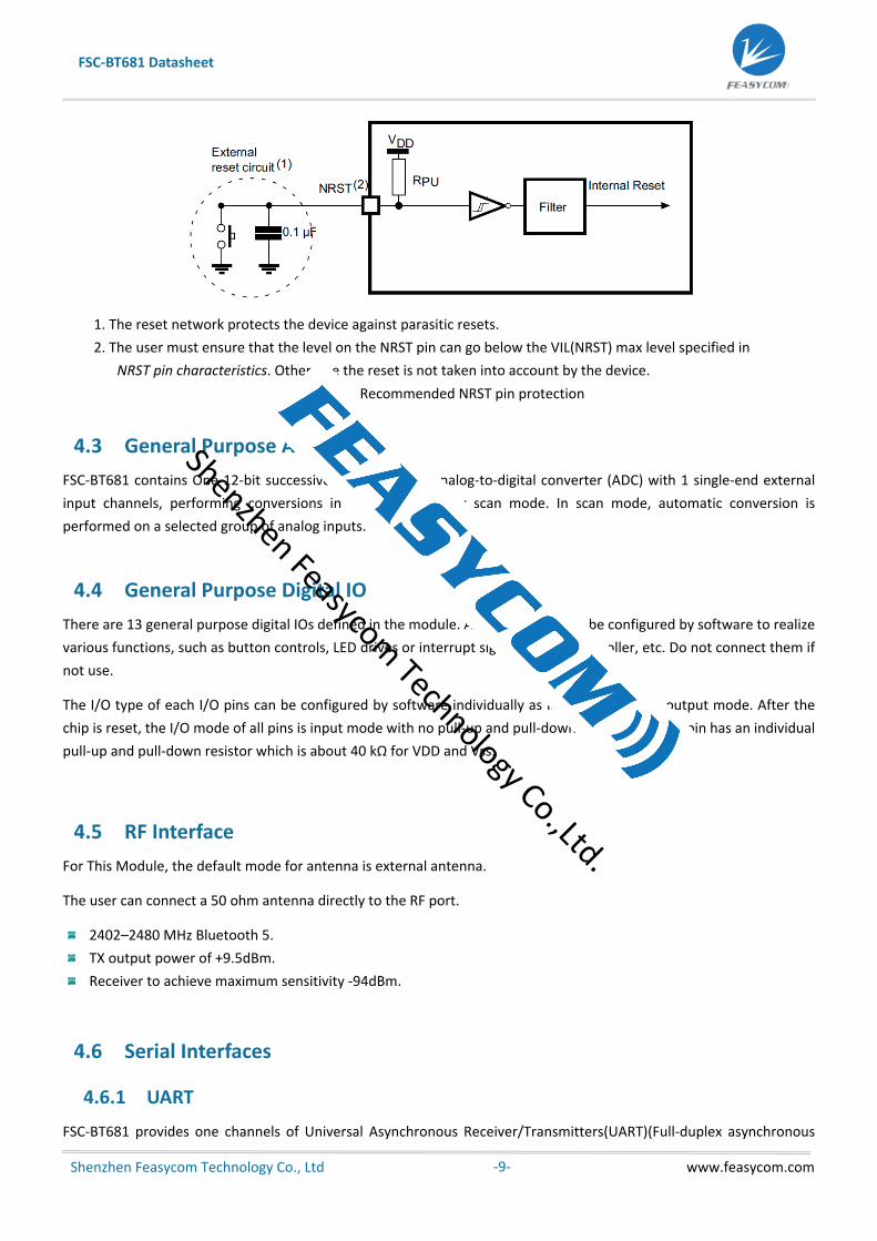
1. The reset network protects the device against parasitic resets.
2. The user must ensure that the level on the NRST pin can go below the VIL(NRST) max level specified in
NRST pin characteristics. Otherwise the reset is not taken into account by the device.
Figure 4:Recommended NRST pin protection
4.3 General Purpose Analog IO
FSC-BT681 contains One 12-bit successive approximation analog-to-digital converter (ADC) with 1 single-end external
input channels, performing conversions in the single-shot or scan mode. In scan mode, automatic conversion is
performed on a selected group of analog inputs.
4.4 General Purpose Digital IO
There are 13 general purpose digital IOs defined in the module. All these GPIOs can be configured by software to realize
various functions, such as button controls, LED drives or interrupt signals to host controller, etc. Do not connect them if
not use.
The I/O type of each I/O pins can be configured by software individually as Input or Push-pull output mode. After the
chip is reset, the I/O mode of all pins is input mode with no pull-up and pull-down enable. Each I/O pin has an individual
pull-up and pull-down resistor which is about 40 kΩ for VDD and Vss.
4.5 RF Interface
For This Module, the default mode for antenna is external antenna.
The user can connect a 50 ohm antenna directly to the RF port.
2402–2480 MHz Bluetooth 5.
TX output power of +9.5dBm.
Receiver to achieve maximum sensitivity -94dBm.
4.6 Serial Interfaces
4.6.1 UART
FSC-BT681 provides one channels of Universal Asynchronous Receiver/Transmitters(UART)(Full-duplex asynchronous
Shenzhen Feasycom Technology Co.,Ltd.

FSC-BT681 Datasheet
Shenzhen Feasycom Technology Co., Ltd www.feasycom.com -10-
communications). The UART Controller performs a serial-to-parallel conversion on data received from the peripheral and
a parallel-to-serial conversion on data transmitted from the CPU. Each UART Controller channel supports ten types of
interrupts.
This is a standard UART interface for communicating with other serial devices. The UART interface provides a simple
mechanism for communicating with other serial devices using the RS232 protocol.
When the module is connected to another digital device, UART_RX and UART_TX transfer data between the two devices.
The remaining two signals, UART_CTS and UART_RTS, can be used to implement RS232 hardware flow control where
both are active low indicators.
This module output is at 3.3V CMOS logic levels (tracks VCC). Level conversion must be added to interface with an RS-
232 level compliant interface.
Some serial implementations link CTS and RTS to remove the need for handshaking. We do not recommend linking CTS
and RTS except for testing and prototyping. If these pins are linked and the host sends data when the FSC-BT681 deasserts
its RTS signal, there is significant risk that internal receive buffers will overflow, which could lead to an internal processor
crash. This drops the connection and may require a power cycle to reset the module. We recommend that you adhere
to the correct CTS/RTS handshaking protocol for proper operation.
Table 4: Possible UART Settings
Parameter Possible Values
Baudrate
Minimum 1200 baud (≤2%Error)
Standard 115200bps(≤1%Error)
Maximum 921600bps(≤1%Error)
Flow control RTS/CTS, or None
Parity None, Odd or Even
Number of stop bits 1 or 2
Bits per channel 5/6/7/8
When connecting the module to a host, please make sure to follow .
Module Host
TX RXRX TX
GND GND
RTSRTSCTS
CTS
Figure 5: UART Connection
Shenzhen Feasycom Technology Co.,Ltd.

FSC-BT681 Datasheet
Shenzhen Feasycom Technology Co., Ltd www.feasycom.com -11-
4.6.2 I2C Interface
I2C is a two-wire, bi-directional serial bus that provides a simple and efficient method of data exchange between devices.
The I2C standard is a true multi-master bus including collision detection and arbitration that prevents data corruption if
two or more masters attempt to control the bus simultaneously.
Data is transferred between a Master and a Slave synchronously to SCL on the SDA line on a byte-by-byte basis. Each
data byte is 8-bit long. There is one SCL clock pulse for each data bit with the MSB being transmitted first. An acknowledge
bit follows each transferred byte. Each bit is sampled during the high period of SCL; therefore, the SDA line may be
changed only during the low period of SCL and must be held stable during the high period of SCL. A transition on the SDA
line while SCL is high is interpreted as a command (START or STOP). Please refer to the following figure for more details
about I2C Bus Timing.
Figure 6: I2C Bus Timing
The device on-chip I2C logic provides the serial interface that meets the I2C bus standard mode specification. The I2C
port handles byte transfers autonomously. The I2C H/W interfaces to the I2C bus via two pins: SDA and SCL. Pull up
resistor is needed for I2C operation as these are open drain pins. When the I/O pins are used as I2C port, user must set
the pins function to I2C in advance.
4.7 PWM Generator and Capture Timer (PWM)
The PWM is designed to generate programmable pulse width of outputs. There is one timer to count cycles of the peripheral clock(PCLK) and can optionally generate interrupts or perform other actions at specified timer values based on 2 set of four match registers. The peripheral clock is provided by the system clock
5. ELECTRICAL CHARACTERISTICS
5.1 Absolute Maximum Ratings
Absolute maximum ratings for supply voltage and voltages on digital and analogue pins of the module are listed below.
Exceeding these values causes permanent damage.
The average PIO pin output current is defined as the average current value flowing through any one of the corresponding
pins for a 100mS period. The total average PIO pin output current is defined as the average current value flowing through
all of the corresponding pins for a 100mS period. The maximum output current is defined as the value of the peak current
flowing through any one of the corresponding pins.
Shenzhen Feasycom Technology Co.,Ltd.
FSC-BT681 Datasheet
Shenzhen Feasycom Technology Co., Ltd www.feasycom.com -12-
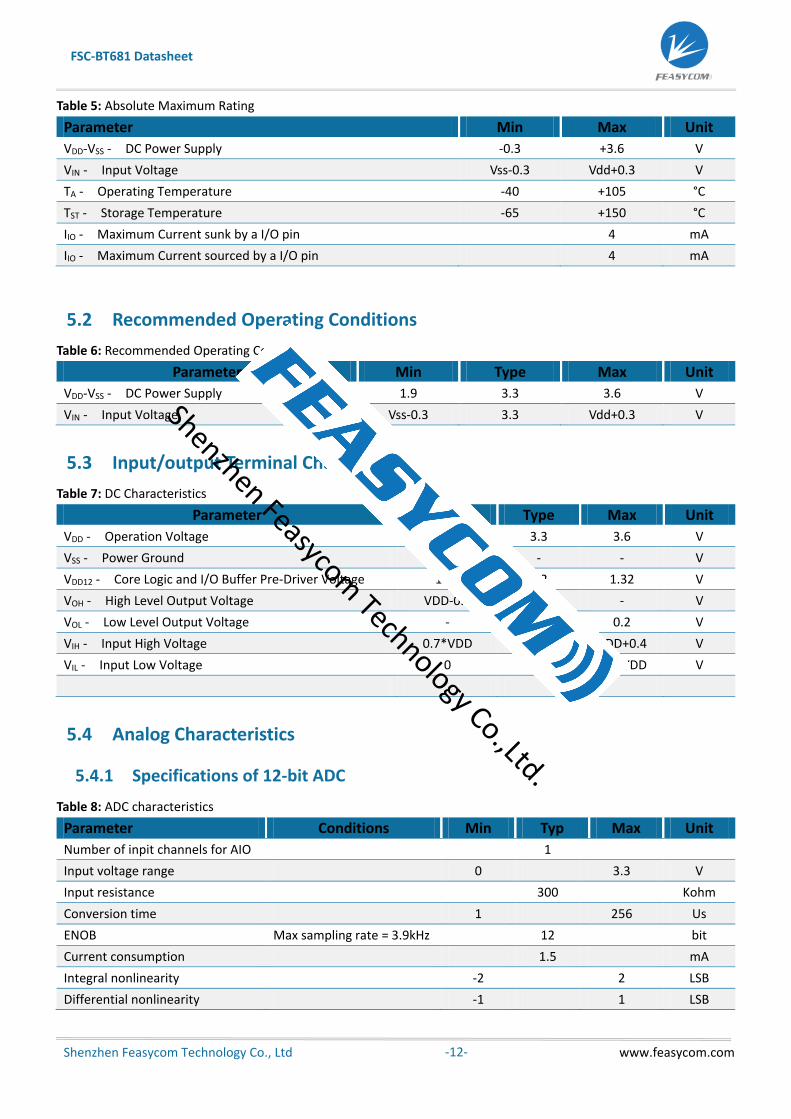
Table 5: Absolute Maximum Rating
Parameter Min Max Unit
VDD-VSS - DC Power Supply -0.3 +3.6 V
VIN - Input Voltage Vss-0.3 Vdd+0.3 V
TA - Operating Temperature -40 +105 °C
TST - Storage Temperature -65 +150 °C
IIO - Maximum Current sunk by a I/O pin 4 mA
IIO - Maximum Current sourced by a I/O pin 4 mA
5.2 Recommended Operating Conditions
Table 6: Recommended Operating Conditions
Parameter Min Type Max Unit
VDD-VSS - DC Power Supply 1.9 3.3 3.6 V
VIN - Input Voltage Vss-0.3 3.3 Vdd+0.3 V
5.3 Input/output Terminal Characteristics
Table 7: DC Characteristics
Parameter Min Type Max Unit
VDD - Operation Voltage 1.9 3.3 3.6 V
VSS - Power Ground -0.3 - - V
VDD12 - Core Logic and I/O Buffer Pre-Driver Voltage 1.08 1.2 1.32 V
VOH - High Level Output Voltage VDD-0.2 - - V
VOL - Low Level Output Voltage - - 0.2 V
VIH - Input High Voltage 0.7*VDD - VDD+0.4 V
VIL - Input Low Voltage 0 - 0.3*VDD V
5.4 Analog Characteristics
5.4.1 Specifications of 12-bit ADC
Table 8: ADC characteristics
Parameter Conditions Min Typ Max Unit
Number of inpit channels for AIO 1
Input voltage range 0 3.3 V
Input resistance 300 Kohm
Conversion time 1 256 Us
ENOB Max sampling rate = 3.9kHz 12 bit
Current consumption 1.5 mA
Integral nonlinearity -2 2 LSB
Differential nonlinearity -1 1 LSB
Shenzhen Feasycom Technology Co.,Ltd.
FSC-BT681 Datasheet
Shenzhen Feasycom Technology Co., Ltd www.feasycom.com -13-
5.5 I2C Dynamic Characteristics
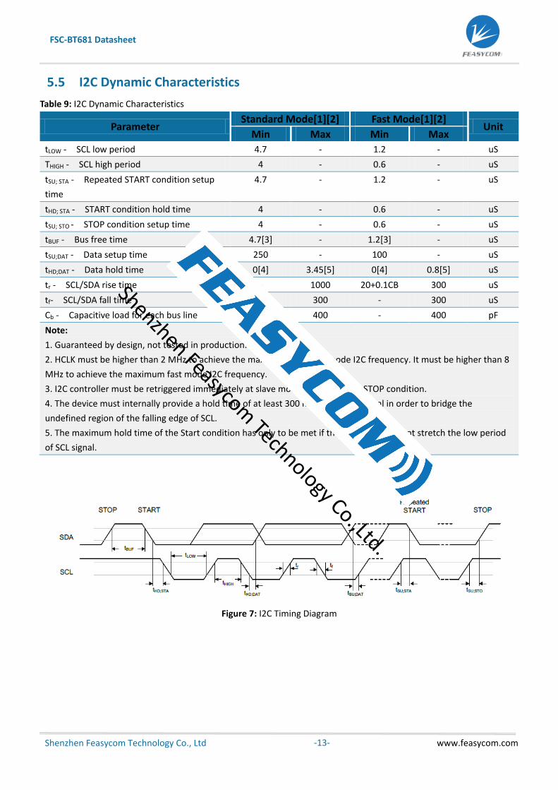
Table 9: I2C Dynamic Characteristics
Parameter Standard Mode[1][2] Fast Mode[1][2]
Unit Min Max Min Max
tLOW - SCL low period 4.7 - 1.2 - uS
THIGH - SCL high period 4 - 0.6 - uS
tSU; STA - Repeated START condition setup
time
4.7 - 1.2 - uS
tHD; STA - START condition hold time 4 - 0.6 - uS
tSU; STO - STOP condition setup time 4 - 0.6 - uS
tBUF - Bus free time 4.7[3] - 1.2[3] - uS
tSU;DAT - Data setup time 250 - 100 - uS
tHD;DAT - Data hold time 0[4] 3.45[5] 0[4] 0.8[5] uS
tr - SCL/SDA rise time - 1000 20+0.1CB 300 uS
tf- SCL/SDA fall time - 300 - 300 uS
Cb - Capacitive load for each bus line - 400 - 400 pF
Note:
1. Guaranteed by design, not tested in production.
2. HCLK must be higher than 2 MHz to achieve the maximum standard mode I2C frequency. It must be higher than 8
MHz to achieve the maximum fast mode I2C frequency.
3. I2C controller must be retriggered immediately at slave mode after receiving STOP condition.
4. The device must internally provide a hold time of at least 300 ns for the SDA signal in order to bridge the
undefined region of the falling edge of SCL.
5. The maximum hold time of the Start condition has only to be met if the interface does not stretch the low period
of SCL signal.
Figure 7: I2C Timing Diagram
Shenzhen Feasycom Technology Co.,Ltd.

FSC-BT681 Datasheet
Shenzhen Feasycom Technology Co., Ltd www.feasycom.com -14-
5.6 Power consumptions
Table 10: Power consumptions Parameter Test Conditions Type Unit
Tx current @9.5dBm VDD=3V, Tx=9.5dBm, LEDs disconnected. ~35 mA
Rx current @1Mbps 4.76 mA
Sleep VDD=3V, Tx=9.5dBm, LEDs disconnected. 4 uA
Deepsleep VDD=3V, Tx=9.5dBm, LEDs disconnected. 0.5 uA
Shut down mode VDD=3V, Tx=9.5dBm, LEDs disconnected. 0.1 uA
6. MSL & ESD
Table 11: MSL and ESD
Parameter Value
MSL grade: MSL 3
ESD grade: Human Body Model: Class-2
Machine Model: Class-B
7. RECOMMENDED TEMPERATURE REFLOW PROFILE
Prior to any reflow, it is important to ensure the modules were packaged to prevent moisture absorption. New packages contain desiccate (to absorb moisture) and a humidity indicator card to display the level maintained during storage and shipment. If directed to bake units on the card, please check the below Table 11 and follow instructions specified by IPC/JEDEC J-STD-033.
Note: The shipping tray cannot be heated above 65°C. If baking is required at the higher temperatures displayed in the below Table 11, the modules must be removed from the shipping tray.
Any modules not manufactured before exceeding their floor life should be re-packaged with fresh desiccate and a new humidity indicator card. Floor life for MSL (Moisture Sensitivity Level) 3 devices is 168 hours in ambient environment 30°C/60%RH.
Table 11: Recommended baking times and temperatures
MSL
125°C Baking Temp. 90°C/≤ 5%RH Baking Temp. 40°C/ ≤ 5%RH Baking Temp.
Saturated @
30°C/85%
Floor Life Limit
+ 72 hours @
30°C/60%
Saturated @
30°C/85%
Floor Life Limit
+ 72 hours @
30°C/60%
Saturated @
30°C/85%
Floor Life Limit
+ 72 hours @
30°C/60%
3 9 hours 7 hours 33 hours 23 hours 13 days 9 days
Feasycom surface mount modules are designed to be easily manufactured, including reflow soldering to a PCB. Ultimately it is the responsibility of the customer to choose the appropriate solder paste and to ensure oven temperatures during reflow meet the requirements of the solder paste. Feasycom surface mount modules conform to J-STD-020D1 standards for reflow temperatures.
The soldering profile depends on various parameters necessitating a set up for each application. The data here is given only for guidance on solder reflow.
Shenzhen Feasycom Technology Co.,Ltd.

FSC-BT681 Datasheet
Shenzhen Feasycom Technology Co., Ltd www.feasycom.com -15-
210 217
250
A B C D
1 2 0
25
3 4 5 6 min
E
Figure 8: Typical Lead-free Re-flow
Pre-heat zone (A) — This zone raises the temperature at a controlled rate, typically 0.5 – 2 C/s. The purpose of this zone is to preheat the PCB board and components to 120 ~ 150 C. This stage is required to distribute the heat uniformly to the PCB board and completely remove solvent to reduce the heat shock to components.
Equilibrium Zone 1 (B) — In this stage the flux becomes soft and uniformly encapsulates solder particles and spread over PCB board, preventing them from being re-oxidized. Also with elevation of temperature and liquefaction of flux, each activator and rosin get activated and start eliminating oxide film formed on the surface of each solder particle and PCB board. The temperature is recommended to be 150 to 210 for 60 to 120 second for this zone.
Equilibrium Zone 2 (C) (optional) — In order to resolve the upright component issue, it is recommended to keep the temperature in 210 – 217 for about 20 to 30 second.
Reflow Zone (D) — The profile in the figure is designed for Sn/Ag3.0/Cu0.5. It can be a reference for other lead-free solder. The peak temperature should be high enough to achieve good wetting but not so high as to cause component discoloration or damage. Excessive soldering time can lead to intermetallic growth which can result in a brittle joint. The recommended peak temperature (Tp) is 230 ~ 250 C. The soldering time should be 30 to 90 second when the temperature is above 217 C.
Cooling Zone (E) — The cooling ate should be fast, to keep the solder grains small which will give a longer-lasting joint. Typical cooling rate should be 4 C.
Shenzhen Feasycom Technology Co.,Ltd.

FSC-BT681 Datasheet
Shenzhen Feasycom Technology Co., Ltd www.feasycom.com -16-
8. MECHANICAL DETAILS
8.1 Mechanical Details
Dimension: 10mm(W) x 11.9mm(L) x 1.7mm(H) Tolerance: ±0.1mm
Module size: 10mm X 11.9mm Tolerance: ±0.1mm
Pad size: 0.9mmX0.6mm Tolerance: ±0.1mm
Pad pitch: 1.1mm Tolerance: ±0.1mm
Figure 9: FSC-BT681 footprint
9. HARDWARE INTEGRATION SUGGESTIONS
9.1 Soldering Recommendations
FSC-BT681 is compatible with industrial standard reflow profile for Pb-free solders. The reflow profile used is dependent on the thermal mass of the entire populated PCB, heat transfer efficiency of the oven and particular type of solder paste used. Consult the datasheet of particular solder paste for profile configurations.
Feasycom will give following recommendations for soldering the module to ensure reliable solder joint and operation of the module after soldering. Since the profile used is process and layout dependent, the optimum profile should be studied case by case. Thus following recommendation should be taken as a starting point guide.
9.2 Layout Guidelines(Internal Antenna)
It is strongly recommended to use good layout practices to ensure proper operation of the module. Placing copper or any metal near antenna deteriorates its operation by having effect on the matching properties. Metal shield around the antenna will prevent the radiation and thus metal case should not be used with the module. Use grounding vias separated max 3 mm apart at the edge of grounding areas to prevent RF penetrating inside the PCB and causing an unintentional
Shenzhen Feasycom Technology Co.,Ltd.

FSC-BT681 Datasheet
Shenzhen Feasycom Technology Co., Ltd www.feasycom.com -17-
resonator. Use GND vias all around the PCB edges.
The mother board should have no bare conductors or vias in this restricted area, because it is not covered by stop mask print. Also no copper (planes, traces or vias) are allowed in this area, because of mismatching the on-board antenna.
5
26.9
Max.0.5
20 10
43
.5
13
18M
ax.0
.5
10
20
Applic. PCB
no bare copper(exept solder pads for module)
no copper and components on any layer
no components on any layer
do not place any conductive parts in this area
Provide solid ground plane(s) as large as possible around area
Figure 10: FSC-BT681 Restricted Area
Following recommendations helps to avoid EMC problems arising in the design. Note that each design is unique and the following list do not consider all basic design rules such as avoiding capacitive coupling between signal lines. Following list is aimed to avoid EMC problems caused by RF part of the module. Use good consideration to avoid problems arising from digital signals in the design.
Ensure that signal lines have return paths as short as possible. For example if a signal goes to an inner layer through a via, always use ground vias around it. Locate them tightly and symmetrically around the signal vias. Routing of any sensitive signals should be done in the inner layers of the PCB. Sensitive traces should have a ground area above and under the line. If this is not possible, make sure that the return path is short by other means (for example using a ground line next to the signal line).
9.3 Layout Guidelines(External Antenna)
Placement and PCB layout are critical to optimize the performances of a module without on-board antenna designs. The trace from the antenna port of the module to an external antenna should be 50 and must be as short as possible to avoid any interference into the transceiver of the module. The location of the external antenna and RF-IN port of the module should be kept away from any noise sources and digital traces. A matching network might be needed in between the external antenna and RF-IN port to better match the impedance to minimize the return loss.
As indicated in Figure 16 below, RF critical circuits of the module should be clearly separated from any digital circuits on the system board. All RF circuits in the module are close to the antenna port. The module, then, should be placed in this way that module digital part towards your digital section of the system PCB.
Shenzhen Feasycom Technology Co.,Ltd.

FSC-BT681 Datasheet
Shenzhen Feasycom Technology Co., Ltd www.feasycom.com -18-
An
tenn
a
RF_IN
Digital Part
Non enmitting circuits
Non enmitting circuits
Digital & Analog Circuits
PCB
An
ten
na
RF & heat enmitting
circuits
Digital Part
RF_IN
Digital & Analog Circuits
RF & heat enmitting
circuits
PCB
Figure 11: Placement the Module on a System Board
9.3.1 Antenna Connection and Grounding Plane Design
AntennaMatchingNetwork
5mmRF_IN
Figure 12: Leave 5mm Clearance Space from the Antenna
General design recommendations are:
The length of the trace or connection line should be kept as short as possible.
Distance between connection and ground area on the top layer should at least be as large as the dielectric thickness.
Routing the RF close to digital sections of the system board should be avoided.
To reduce signal reflections, sharp angles in the routing of the micro strip line should be avoided. Chamfers or fillets are preferred for rectangular routing; 45-degree routing is preferred over Manhattan style 90-degree routing.
Shenzhen Feasycom Technology Co.,Ltd.

FSC-BT681 Datasheet
Shenzhen Feasycom Technology Co., Ltd www.feasycom.com -19-
An
tenn
a
An
tenn
a
An
tenn
a
PCB PCB PCB
Wrong Better Best
Figure 13: Recommended Trace Connects Antenna and the Module
Routing of the RF-connection underneath the module should be avoided. The distance of the micro strip line to the ground plane on the bottom side of the receiver is very small and has huge tolerances. Therefore, the impedance of this part of the trace cannot be controlled.
Use as many vias as possible to connect the ground planes.
10. PRODUCT PACKAGING INFORMATION
10.1 Default Packing
a, Tray vacuum
b, Tray Dimension: 180mm * 195mm
Shenzhen Feasycom Technology Co.,Ltd.

FSC-BT681 Datasheet
Shenzhen Feasycom Technology Co., Ltd www.feasycom.com -20-
Figure 14: Tray vacuum (Image for reference only, subject to actual product)
Shenzhen Feasycom Technology Co.,Ltd.

FSC-BT681 Datasheet
Shenzhen Feasycom Technology Co., Ltd www.feasycom.com -21-
11. APPLICATION SCHEMATIC
UART interface
3.3V Level of voltage
H = instruction modeL = throughput mode
When bluetooth connection established,
DEBUG Interface (Optional)
a rising edge of GPIO3 will cause disconnection with remote device.
BT work Status Indicator Light
Bluetooth connection status:
When bluetooth connection established,
H = ConnectedL = No connection
1
2
1
2
3
4
5
6
8
9
10 13
14
15
16
17
18
19
20
21
22
7
11 12
RESET
3V3_BT
MCU_RX
MCU_TX
MCU_CTS
MCU_RTS
TRANSFER_MODE
3V3_BT
RESET
DISCONNECT
PIO10
MCU_RX
MCU_TX
GPIO2
GPIO2
OD_GPIO1
OD_GPIO1
DEBUG_TX
DEBUG_RX
DEBUG_TX
DEBUG_RX
C54
100nF
C4
10uF
TP3
TP4
TP5
TP6
TP7
J1
ANT-F
R2 0R
C1
NC
C2
NC
LEDR13 1K
GPIO11/UART_RTS
GPIO10/UART_CTS
UART_TX
UART_RX
OD_GPIO0/I2C_SDA
OD_GPIO1/I2C_SCL
RESET
VDD_3V3
GND GPIO6/SPI_CS
GPIO7/SPI_MOSI
GPIO8/SPI_MISO
GPIO9/SPI_CLK
GPIO3/DISC
GPIO2
GPIO4/LED
GPIO0/STATUS
GND
EXT_ANT
GPIO16/AIO
DEBUG_TX
DEBUG_RX
U4
FSC-BT681
TP2
TP1
TP8
TP9
RESET (Optional)
Reset Circuit Based On Voltage Dual Comparators
Reset pin can be left floating or controlled by the MCU IO portPOWER (Optional)
3.3V LDO
1 2
3
1
2
3 4
5
1
2
RESET
3V3_BT
3V3_BT5V
R4 100K
GND RESET
VCC
U3
CN809R-2.63V
C3
10uF
C5
100nFC6
100nF
C7
10uF
VIN
GNDEN BP
VOUT
U5
C8
100nF
J2
Shenzhen Feasycom Technology Co.,Ltd.