bga7027 400 mhz to 2700 mhz 0.5 w high linearity …. product profile 1.1 general description the...
TRANSCRIPT
1. Product profile
1.1 General description
The BGA7027 MMIC is a one-stage amplifier, offered in a low-cost surface-mount package. It delivers 28 dBm output power at 1 dB gain compression and a superior performance up to 2700 MHz.
1.2 Features and benefits
400 MHz to 2700 MHz frequency operating range
11 dB small signal gain at 2 GHz
28 dBm output power at 1 dB gain compression
Integrated active biasing
External matching allows broad application optimization of the electrical performance
5 V single supply operation
ESD protection at all pins
1.3 Applications
1.4 Quick reference data
[1] Operation outside this range is possible but not guaranteed.
[2] PL = 17 dBm per tone; spacing = 1 MHz.
BGA7027400 MHz to 2700 MHz 0.5 W high linearity silicon amplifierRev. 2 — 26 November 2010 Product data sheet
Broadband CPE/MoCA Industrial applications
WLAN/ISM/RFID E-metering
Wireless infrastructure (base station, repeater, backhaul systems)
Satellite Master Antenna TV (SMATV)
Table 1. Quick reference dataInput and output impedances matched to 50 . Typical values at: VCC = 5 V; Tcase = 25 C; unless otherwise specified.
Symbol Parameter Conditions Min Typ Max Unit
f frequency [1] 400 - 2700 MHz
Gp power gain f = 2140 MHz 9.0 11.0 13.0 dB
PL(1dB) output power at 1 dB gain compression f = 2140 MHz 26 28 - dBm
IP3O output third-order intercept point f = 2140 MHz [2] 40.0 42.5 - dBm

NXP Semiconductors BGA7027400 MHz to 2700 MHz 0.5 W high linearity silicon amplifier
2. Pinning information
[1] This pin is DC-coupled and requires an external DC-blocking capacitor.
[2] The center metal base of the SOT89 also functions as heatsink for the power amplifier.
3. Ordering information
4. Functional diagram
Table 2. Pinning
Pin Description Simplified outline Graphic symbol
1 VCC(RF)[1]
2 GND [2]
3 RF_IN [1]
3 2 1 sym130
2
13
Table 3. Ordering information
Type number Package
Name Description Version
BGA7027 - plastic surface-mounted package; exposed die pad for good heat transfer; 3 leads
SOT89
Fig 1. Functional diagram
BANDGAPBIAS
ENABLEV/I
CONVERTER
VCC(RF)
GND
1
2
3RF_IN
014aab020
BGA7027 All information provided in this document is subject to legal disclaimers. © NXP B.V. 2010. All rights reserved.
Product data sheet Rev. 2 — 26 November 2010 2 of 21
NXP Semiconductors BGA7027400 MHz to 2700 MHz 0.5 W high linearity silicon amplifier
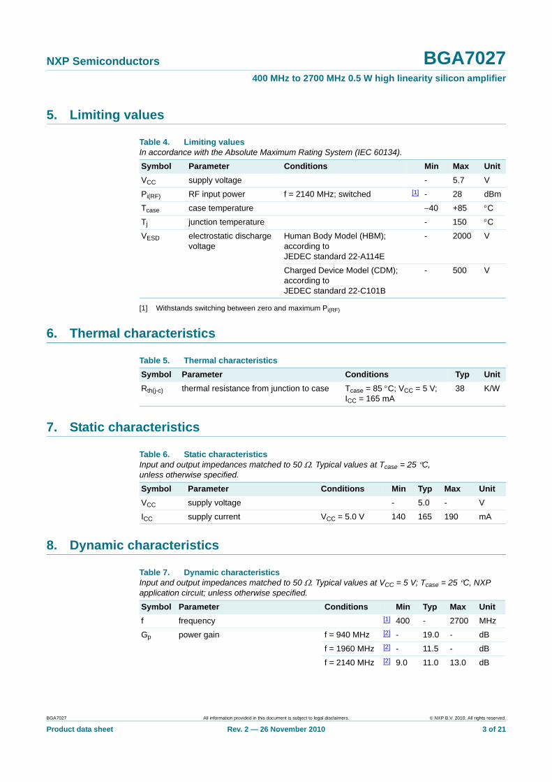
5. Limiting values
[1] Withstands switching between zero and maximum Pi(RF)
6. Thermal characteristics
7. Static characteristics
8. Dynamic characteristics
Table 4. Limiting valuesIn accordance with the Absolute Maximum Rating System (IEC 60134).
Symbol Parameter Conditions Min Max Unit
VCC supply voltage - 5.7 V
Pi(RF) RF input power f = 2140 MHz; switched [1] - 28 dBm
Tcase case temperature 40 +85 C
Tj junction temperature - 150 C
VESD electrostatic discharge voltage
Human Body Model (HBM); according to JEDEC standard 22-A114E
- 2000 V
Charged Device Model (CDM); according to JEDEC standard 22-C101B
- 500 V
Table 5. Thermal characteristics
Symbol Parameter Conditions Typ Unit
Rth(j-c) thermal resistance from junction to case Tcase = 85 C; VCC = 5 V; ICC = 165 mA
38 K/W
Table 6. Static characteristicsInput and output impedances matched to 50 . Typical values at Tcase = 25 C, unless otherwise specified.
Symbol Parameter Conditions Min Typ Max Unit
VCC supply voltage - 5.0 - V
ICC supply current VCC = 5.0 V 140 165 190 mA
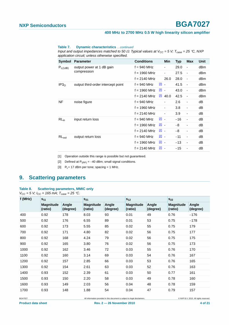
Table 7. Dynamic characteristicsInput and output impedances matched to 50 . Typical values at VCC = 5 V; Tcase = 25 C, NXP application circuit; unless otherwise specified.
Symbol Parameter Conditions Min Typ Max Unit
f frequency [1] 400 - 2700 MHz
Gp power gain f = 940 MHz [2] - 19.0 - dB
f = 1960 MHz [2] - 11.5 - dB
f = 2140 MHz [2] 9.0 11.0 13.0 dB
BGA7027 All information provided in this document is subject to legal disclaimers. © NXP B.V. 2010. All rights reserved.
Product data sheet Rev. 2 — 26 November 2010 3 of 21
NXP Semiconductors BGA7027400 MHz to 2700 MHz 0.5 W high linearity silicon amplifier
[1] Operation outside this range is possible but not guaranteed.
[2] Defined at Pi(RF) = 40 dBm; small signal conditions.
[3] PL= 17 dBm per tone; spacing = 1 MHz.
9. Scattering parameters
PL(1dB) output power at 1 dB gain compression
f = 940 MHz - 29.0 - dBm
f = 1960 MHz - 27.5 - dBm
f = 2140 MHz 26.0 28.0 - dBm
IP3O output third-order intercept point f = 940 MHz [3] - 41.5 - dBm
f = 1960 MHz [3] - 43.0 - dBm
f = 2140 MHz [3] 40.0 42.5 - dBm
NF noise figure f = 940 MHz - 2.6 - dB
f = 1960 MHz - 3.8 - dB
f = 2140 MHz - 3.9 - dB
RLin input return loss f = 940 MHz [2] - 16 - dB
f = 1960 MHz [2] - 8 - dB
f = 2140 MHz [2] - 8 - dB
RLout output return loss f = 940 MHz [2] - 11 - dB
f = 1960 MHz [2] - 13 - dB
f = 2140 MHz [2] - 15 - dB
Table 7. Dynamic characteristics …continuedInput and output impedances matched to 50 . Typical values at VCC = 5 V; Tcase = 25 C, NXP application circuit; unless otherwise specified.
Symbol Parameter Conditions Min Typ Max Unit
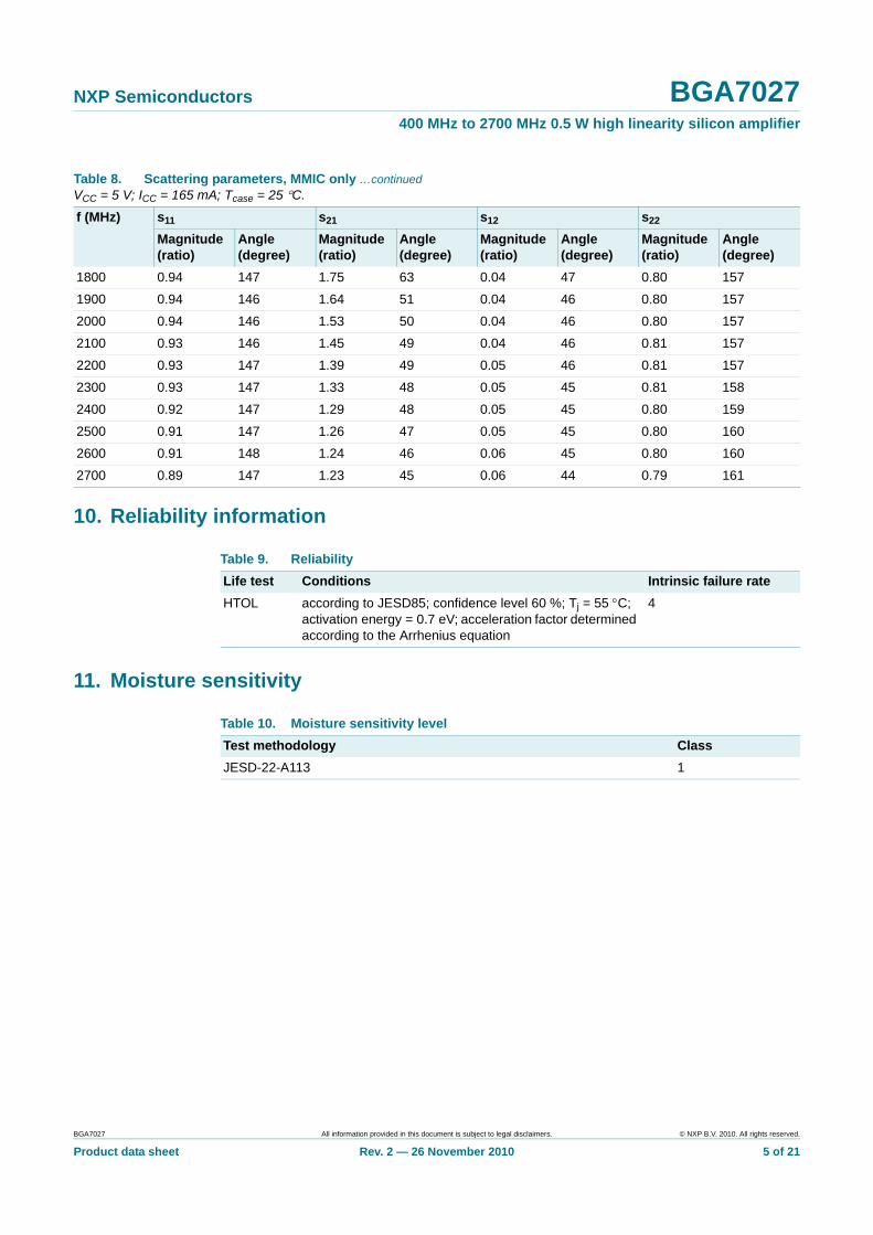
Table 8. Scattering parameters, MMIC onlyVCC = 5 V; ICC = 165 mA; Tcase = 25 C.
f (MHz) s11 s21 s12 s22
Magnitude (ratio)
Angle (degree)
Magnitude (ratio)
Angle (degree)
Magnitude (ratio)
Angle (degree)
Magnitude (ratio)
Angle (degree)
400 0.92 178 8.03 93 0.01 49 0.76 176
500 0.92 176 6.55 89 0.01 53 0.75 178
600 0.92 173 5.55 85 0.02 55 0.75 179
700 0.92 171 4.80 82 0.02 56 0.75 177
800 0.92 168 4.24 79 0.02 56 0.75 175
900 0.92 165 3.80 76 0.02 56 0.75 173
1000 0.92 162 3.46 72 0.03 55 0.76 170
1100 0.92 160 3.14 69 0.03 54 0.76 167
1200 0.92 157 2.85 66 0.03 53 0.76 165
1300 0.92 154 2.61 63 0.03 52 0.76 163
1400 0.93 152 2.39 61 0.03 50 0.77 161
1500 0.93 150 2.20 58 0.03 49 0.78 160
1600 0.93 149 2.03 56 0.04 48 0.78 159
1700 0.93 148 1.88 54 0.04 47 0.79 157
BGA7027 All information provided in this document is subject to legal disclaimers. © NXP B.V. 2010. All rights reserved.
Product data sheet Rev. 2 — 26 November 2010 4 of 21
NXP Semiconductors BGA7027400 MHz to 2700 MHz 0.5 W high linearity silicon amplifier
10. Reliability information
11. Moisture sensitivity
1800 0.94 147 1.75 63 0.04 47 0.80 157
1900 0.94 146 1.64 51 0.04 46 0.80 157
2000 0.94 146 1.53 50 0.04 46 0.80 157
2100 0.93 146 1.45 49 0.04 46 0.81 157
2200 0.93 147 1.39 49 0.05 46 0.81 157
2300 0.93 147 1.33 48 0.05 45 0.81 158
2400 0.92 147 1.29 48 0.05 45 0.80 159
2500 0.91 147 1.26 47 0.05 45 0.80 160
2600 0.91 148 1.24 46 0.06 45 0.80 160
2700 0.89 147 1.23 45 0.06 44 0.79 161
Table 8. Scattering parameters, MMIC only …continuedVCC = 5 V; ICC = 165 mA; Tcase = 25 C.
f (MHz) s11 s21 s12 s22
Magnitude (ratio)
Angle (degree)
Magnitude (ratio)
Angle (degree)
Magnitude (ratio)
Angle (degree)
Magnitude (ratio)
Angle (degree)
Table 9. Reliability
Life test Conditions Intrinsic failure rate
HTOL according to JESD85; confidence level 60 %; Tj = 55 C; activation energy = 0.7 eV; acceleration factor determined according to the Arrhenius equation
4
Table 10. Moisture sensitivity level
Test methodology Class
JESD-22-A113 1
BGA7027 All information provided in this document is subject to legal disclaimers. © NXP B.V. 2010. All rights reserved.
Product data sheet Rev. 2 — 26 November 2010 5 of 21

NXP Semiconductors BGA7027400 MHz to 2700 MHz 0.5 W high linearity silicon amplifier
12. Application information
12.1 920 MHz to 960 MHz
See Table 11 for a list of components.
PCB board specification:
Rogers RO4003C; Height = 0.508 mm; r = 3.38; Copper thickness = 35 m.
Fig 2. 920 MHz to 960 MHz application schematic
C4 C5
C6
C8
C9
C7
R1
L1C10
L2
C1MSL1 MSL2 MSL3 MSL9MSL6 MSL7 MSL8RF_IN
BGA7027
50 Ω 50 Ω
VCC
001aam066
MSL5VCC(RF)MSL4
C2 C3
(1) Tcase = 25 C.
(2) Tcase = 85 C.
(3) Tcase = 40 C.
(1) Tcase = 25 C.
(2) Tcase = 85 C.
(3) Tcase = 40 C.
Fig 3. Output power at 1 dB gain compression as a function of frequency
Fig 4. Power gain as a function of frequency
001aam130
f (GHz)0.92 0.960.950.940.93
26
28
24
30
32
PL(1dB)(dBm)
22
(1)
(2)
(3)
001aam131
f (GHz)0.92 0.93 0.960.950.94
20
22
18
24
26
Gp(dB)
16
(1)(2)(3)
BGA7027 All information provided in this document is subject to legal disclaimers. © NXP B.V. 2010. All rights reserved.
Product data sheet Rev. 2 — 26 November 2010 6 of 21

NXP Semiconductors BGA7027400 MHz to 2700 MHz 0.5 W high linearity silicon amplifier
Tcase = 25 C.
(1) RLin.
(2) RLout.
(3) ISL.
PL = 17 dBm; tone spacing = 1 MHz
(1) Tcase = 25 C.
(2) Tcase = 85 C.
(3) Tcase = 40 C.
Fig 5. Input return loss, output return loss and isolation as a function of frequency
Fig 6. Output third-order intercept point as a function of frequency
001aam132
f (GHz)0.92 0.960.950.940.93
−20
−10
0
−30
(1)
(2)
(3)
RLin, RLout, ISL(dB)
001aam133
f (GHz)0.92 0.960.950.940.93
40
42
38
44
46
IP3O(dBm)
36
(1)(2)(3)
2-carrier W-CDMA; each carrier according to 3GPP test model 1; 64 DPCH; PAR for composite signal = 7.5 dB; 5 MHz carrier spacing.
(1) f = 920 MHz; ACPR measured at f 5 MHz
(2) f = 960 MHz; ACPR measured at f 5 MHz
(3) f = 920 MHz; ACPR measured at f 10 MHz
(4) f = 960 MHz; ACPR measured at f 10 MHz
2-carrier W-CDMA; each carrier according to 3GPP test model 1; 64 DPCH; PAR for composite signal = 9 dB; 10 MHz carrier spacing.
(1) f = 920 MHz; ACPR measured at f 5 MHz
(2) f = 960 MHz; ACPR measured at f 5 MHz
(3) f = 920 MHz; ACPR measured at f 10 MHz
(4) f = 960 MHz; ACPR measured at f 10 MHz
Fig 7. Adjacent channel power ratio as a function of average output power
Fig 8. Adjacent channel power ratio as a function of average output power
PL(AV) (dBm)0 252010 155
001aan073
−40
−60
−20
0
ACPR(dBc)
−80
(1)(2)(3)(4)
PL(AV) (dBm)0 252010 155
001aan074
−40
−60
−20
0
ACPR(dBc)
−80
(1)(2)(3)(4)
BGA7027 All information provided in this document is subject to legal disclaimers. © NXP B.V. 2010. All rights reserved.
Product data sheet Rev. 2 — 26 November 2010 7 of 21

NXP Semiconductors BGA7027400 MHz to 2700 MHz 0.5 W high linearity silicon amplifier
f = 940 MHz; tone spacing = 1 MHz.
(1) Upper sideband
(2) Lower sideband
Fig 9. Output third-order intercept point as a function of output power per tone
PL (dBm) per tone10 181612 14
001aan075
40
45
35
50
55
IP3O(dBm)
30
(1)(2)
See Table 11 for a list of components.
Fig 10. 920 MHz to 960 MHz application reference board
J3
GN
D
VC
C
GN
D
GN
D
GN
D
GN
D
C9
C8
C6C5C4C3C2
C1
L2
C10 L1
C7
MSL9MSL7MSL6 MSL8MSL1 MSL2
MSL3MSL4 MSL5
J1
RF in
J2
RF out
001aam068
R1
BGA7027 All information provided in this document is subject to legal disclaimers. © NXP B.V. 2010. All rights reserved.
Product data sheet Rev. 2 — 26 November 2010 8 of 21

NXP Semiconductors BGA7027400 MHz to 2700 MHz 0.5 W high linearity silicon amplifier
[1] Low Q inductor.
[2] MSL1 to MSL9 dimensions are specified as Width (W), Spacing (S) and Length (L).
Table 11. List of components of 920 MHz to 960 MHzSee Figure 2 and Figure 10 for component layout.Printed-Circuit Board (PCB): Rogers RO4003C stack; height = 0.508 mm; copper plating thickness = 35 m.
Component Description Value Function Remarks
C1, C6 capacitor 68 pF DC blocking Murata, GRM1885C1H680JA01D
C2 capacitor 5.6 pF input match Murata, GRM1885C1H5R6CZ01D
C3 capacitor 2.7 pF input match Murata, GRM1885C1H2R7CZ01D
C4 capacitor 1.0 pF output match Murata, GRM1885C1H1R0CZ01D
C5 capacitor 3.9 pF output match Murata, GRM1885C1H3R9CZ01D
C7 capacitor 68 pF RF decoupling Murata, GRM1885C1H680JA01D
C8 capacitor 100 nF LF decoupling AVX, 0603YC104KAT2A
C9 capacitor 10 F LF decoupling AVX, 1206ZG106ZAT2A
C10 capacitor 68 nF IMD3 suppression Murata, GRM1888R71H683KA93D
J1, J2 RF connector SMA Emerson Network Power, 142-0701-841
J3 DC connector 6 pins MOLEX
L1 inductor 22 nH DC Feed Tyco Electronics, 36501J022JTDG
L2[1] inductor 33 nH IMD3 suppression Tyco Electronics, 36501J033JTDG
MSL1[2] micro stripline 1.14 mm 0.8 mm 10.95 mm input match
MSL2[2] micro stripline 1.14 mm 0.8 mm 4.3 mm input match
MSL3[2] micro stripline 1.14 mm 0.8 mm 1.7 mm input match
MSL4[2] micro stripline 1.14 mm 0.8 mm 4.8 mm input match
MSL5[2] micro stripline 1.14 mm 0.8 mm 2.7 mm output match
MSL6[2] micro stripline 1.14 mm 0.8 mm 3.2 mm output match
MSL7[2] micro stripline 1.14 mm 0.8 mm 4.0 mm output match
MSL8[2] micro stripline 1.14 mm 0.8 mm 1.6 mm output match
MSL9[2] micro stripline 1.14 mm 0.8 mm 10.95 mm output match
R1 resistor 0 Multicomp, MC 0.063W 0603 0R
BGA7027 All information provided in this document is subject to legal disclaimers. © NXP B.V. 2010. All rights reserved.
Product data sheet Rev. 2 — 26 November 2010 9 of 21

NXP Semiconductors BGA7027400 MHz to 2700 MHz 0.5 W high linearity silicon amplifier
12.2 1930 MHz to 1990 MHz
See Table 12 for a list of components.
PCB board specification:
Rogers RO4003C; Height = 0.508 mm; r = 3.38; Copper thickness = 35 m.
Fig 11. 1930 MHz to 1990 MHz application schematic
C3
C4
C6
C7
C5
R1
L1
C8
L2
C1MSL1 MSL2 MSL3 MSL7MSL5 MSL6RF_IN
BGA7027
50 Ω 50 Ω
VCC
001aam069
MSL4VCC(RF)
C2
(1) Tcase = 25 C.
(2) Tcase = 85 C.
(3) Tcase = 40 C.
(1) Tcase = 25 C.
(2) Tcase = 85 C.
(3) Tcase = 40 C.
Fig 12. Output power at 1 dB gain compression as a function of frequency
Fig 13. Power gain as a function of frequency
001aam134
f (GHz)1.93 1.991.971.95
26
28
24
30
32
PL(1dB)(dBm)
22
(1)
(2)
(3)
001aam135
f (GHz)1.93 1.991.971.95
12
14
10
16
18
Gp(dB)
8
(1)(2)(3)
BGA7027 All information provided in this document is subject to legal disclaimers. © NXP B.V. 2010. All rights reserved.
Product data sheet Rev. 2 — 26 November 2010 10 of 21

NXP Semiconductors BGA7027400 MHz to 2700 MHz 0.5 W high linearity silicon amplifier
Tcase = 25 C.
(1) RLin.
(2) RLout.
(3) ISL.
PL = 17 dBm; tone spacing = 1 MHz
(1) Tcase = 25 C.
(2) Tcase = 85 C.
(3) Tcase = 40 C.
Fig 14. Input return loss, output return loss and isolation as a function of frequency
Fig 15. Output third-order intercept point as a function of frequency
001aam136
f (GHz)1.93 1.991.971.95
−20
−10
0
−30
(1)
(2)
(3)
RLin, RLout, ISL(dB)
001aam137
f (GHz)1.93 1.991.971.95
40
42
38
44
46
IP3O(dBm)
36
(1)(2)(3)
See Table 12 for a list of components.
Fig 16. 1930 MHz to 1990 MHz application reference board
J3
GN
D
VC
C
GN
D
GN
D
GN
D
GN
D
C7
C6
C4C3C2
C1
L2
C8 L1
C5
MSL7MSL6MSL5MSL1 MSL2 MSL3MSL4
J1
RF in
J2
RF out
001aam072
R1
BGA7027 All information provided in this document is subject to legal disclaimers. © NXP B.V. 2010. All rights reserved.
Product data sheet Rev. 2 — 26 November 2010 11 of 21

NXP Semiconductors BGA7027400 MHz to 2700 MHz 0.5 W high linearity silicon amplifier
[1] Low Q inductor.
[2] MSL1 to MSL7 dimensions are specified as Width (W), Spacing (S) and Length (L).
12.3 2110 MHz to 2170 MHz
Table 12. List of components of 1930 MHz to 1990 MHzSee Figure 11 and Figure 16 for component layout.Printed-Circuit Board (PCB): Rogers RO4003C stack; height = 0.508 mm; copper plating thickness = 35 m.
Component Description Value Function Remarks
C1, C4 capacitor 15 pF DC blocking Murata, GRM1885C1H150JA01D
C2 capacitor 2.4 pF input match Murata, GRM1885C1H2R4CZ01D
C3 capacitor 2.0 pF output match Murata, GRM1885C1H2R0CZ01D
C5 capacitor 15 pF RF decoupling Murata, GRM1885C1H150JA01D
C6 capacitor 100 nF LF decoupling AVX, 0603YC104KAT2A
C7 capacitor 10 F LF decoupling AVX, 1206ZG106ZAT2A
C8 capacitor 68 nF IMD3 suppression Murata, GRM1888R71H683KA93D
J1, J2 RF connector SMA Emerson Network Power, 142-0701-841
J3 DC connector 6 pins MOLEX
L1 inductor 22 nH DC Feed Tyco Electronics, 36501J022JTDG
L2[1] inductor 33 nH IMD3 suppression Tyco Electronics, 36501J033JTDG
MSL1[2] micro stripline 1.14 mm 0.8 mm 10.95 mm input match
MSL2[2] micro stripline 1.14 mm 0.8 mm 10.6 mm input match
MSL3[2] micro stripline 1.14 mm 0.8 mm 1.0 mm input match
MSL4[2] micro stripline 1.14 mm 0.8 mm 2.7 mm output match
MSL5[2] micro stripline 1.14 mm 0.8 mm 2.0 mm output match
MSL6[2] micro stripline 1.14 mm 0.8 mm 6.8 mm output match
MSL7[2] micro stripline 1.14 mm 0.8 mm 10.95 mm output match
R1 resistor 0 Multicomp. MC 0.063W 0603 0R
See Table 13 for a list of components.
PCB board specification:
Rogers RO4003C; Height = 0.508 mm; r = 3.38; Copper thickness = 35 m.
Fig 17. 2110 MHz to 2170 MHz application schematic
C3
C4
C6
C7
C5
R1
L1
C8
L2
C1MSL1 MSL2 MSL5MSL4RF_IN
BGA7027
50 Ω 50 Ω
VCC
001aam070
MSL3VCC(RF)
C2
BGA7027 All information provided in this document is subject to legal disclaimers. © NXP B.V. 2010. All rights reserved.
Product data sheet Rev. 2 — 26 November 2010 12 of 21

NXP Semiconductors BGA7027400 MHz to 2700 MHz 0.5 W high linearity silicon amplifier
(1) Tcase = 25 C.
(2) Tcase = 85 C.
(3) Tcase = 40 C.
(1) Tcase = 25 C.
(2) Tcase = 85 C.
(3) Tcase = 40 C.
Fig 18. Output power at 1 dB gain compression as a function of frequency
Fig 19. Power gain as a function of frequency
001aam138
f (GHz)2.11 2.172.152.13
26
28
24
30
32
PL(1dB)(dBm)
22
(1)
(2)
(3)
001aam139
f (GHz)2.11 2.172.152.13
12
14
10
16
18
Gp(dB)
8
(1)(2)(3)
Tcase = 25 C.
(1) RLin.
(2) RLout.
(3) ISL.
PL = 17 dBm; tone spacing = 1 MHz
(1) Tcase = 25 C.
(2) Tcase = 85 C.
(3) Tcase = 40 C.
Fig 20. Input return loss, output return loss and isolation as a function of frequency
Fig 21. Output third-order intercept point as a function of frequency
001aam140
f (GHz)2.11 2.172.152.13
−20
−10
0
−30
(1)
(2)
(3)
RLin, RLout, ISL(dB)
001aam141
f (GHz)2.11 2.172.152.13
40
42
38
44
46
IP3O(dBm)
36
(1)(2)(3)
BGA7027 All information provided in this document is subject to legal disclaimers. © NXP B.V. 2010. All rights reserved.
Product data sheet Rev. 2 — 26 November 2010 13 of 21
NXP Semiconductors BGA7027400 MHz to 2700 MHz 0.5 W high linearity silicon amplifier
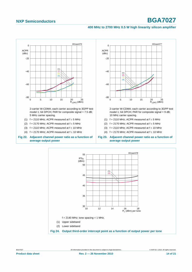
2-carrier W-CDMA; each carrier according to 3GPP test model 1; 64 DPCH; PAR for composite signal = 7.5 dB; 5 MHz carrier spacing.
(1) f = 2110 MHz; ACPR measured at f 5 MHz
(2) f = 2170 MHz; ACPR measured at f 5 MHz
(3) f = 2110 MHz; ACPR measured at f 10 MHz
(4) f = 2170 MHz; ACPR measured at f 10 MHz
2-carrier W-CDMA; each carrier according to 3GPP test model 1; 64 DPCH; PAR for composite signal = 9 dB; 10 MHz carrier spacing.
(1) f = 2110 MHz; ACPR measured at f 5 MHz
(2) f = 2170 MHz; ACPR measured at f 5 MHz
(3) f = 2110 MHz; ACPR measured at f 10 MHz
(4) f = 2170 MHz; ACPR measured at f 10 MHz
Fig 22. Adjacent channel power ratio as a function of average output power
Fig 23. Adjacent channel power ratio as a function of average output power
PL(AV) (dBm)0 252010 155
001aan076
−40
−60
−20
0
ACPR(dBc)
−80
(1)(2)(3)(4)
PL(AV) (dBm)0 252010 155
001aan077
−40
−60
−20
0
ACPR(dBc)
−80
(1)(2)(3)(4)
f = 2140 MHz; tone spacing = 1 MHz.
(1) Upper sideband
(2) Lower sideband
Fig 24. Output third-order intercept point as a function of output power per tone
PL (dBm) per tone10 181612 14
001aan078
40
45
35
50
55
IP3O(dBm)
30
(1)(2)
BGA7027 All information provided in this document is subject to legal disclaimers. © NXP B.V. 2010. All rights reserved.
Product data sheet Rev. 2 — 26 November 2010 14 of 21

NXP Semiconductors BGA7027400 MHz to 2700 MHz 0.5 W high linearity silicon amplifier
See Table 13 for a list of components.
Fig 25. 2110 MHz to 2170 MHz application reference board
J3
GN
D
VC
C
GN
D
GN
D
GN
D
GN
D
C7
C6
C4C3C2
C8
C1
L1
C5
MSL5MSL4MSL1 MSL2
MSL3
J1
RF in
J2
RF out
001aam071
R1
L2
BGA7027 All information provided in this document is subject to legal disclaimers. © NXP B.V. 2010. All rights reserved.
Product data sheet Rev. 2 — 26 November 2010 15 of 21
NXP Semiconductors BGA7027400 MHz to 2700 MHz 0.5 W high linearity silicon amplifier
[1] Low Q inductor.
[2] MSL1 to MSL5 dimensions are specified as Width (W), Spacing (S) and Length (L).
12.4 PCB stack
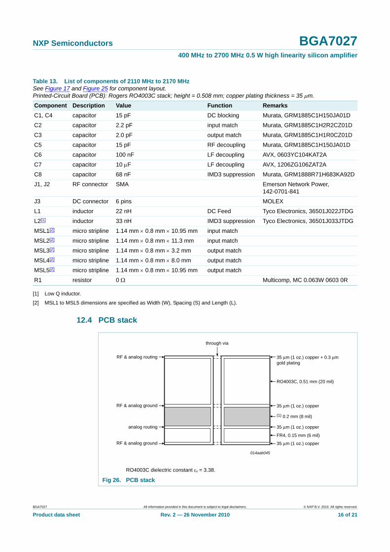
Table 13. List of components of 2110 MHz to 2170 MHzSee Figure 17 and Figure 25 for component layout.Printed-Circuit Board (PCB): Rogers RO4003C stack; height = 0.508 mm; copper plating thickness = 35 m.
Component Description Value Function Remarks
C1, C4 capacitor 15 pF DC blocking Murata, GRM1885C1H150JA01D
C2 capacitor 2.2 pF input match Murata, GRM1885C1H2R2CZ01D
C3 capacitor 2.0 pF output match Murata, GRM1885C1H1R0CZ01D
C5 capacitor 15 pF RF decoupling Murata, GRM1885C1H150JA01D
C6 capacitor 100 nF LF decoupling AVX, 0603YC104KAT2A
C7 capacitor 10 F LF decoupling AVX, 1206ZG106ZAT2A
C8 capacitor 68 nF IMD3 suppression Murata, GRM1888R71H683KA92D
J1, J2 RF connector SMA Emerson Network Power, 142-0701-841
J3 DC connector 6 pins MOLEX
L1 inductor 22 nH DC Feed Tyco Electronics, 36501J022JTDG
L2[1] inductor 33 nH IMD3 suppression Tyco Electronics, 36501J033JTDG
MSL1[2] micro stripline 1.14 mm 0.8 mm 10.95 mm input match
MSL2[2] micro stripline 1.14 mm 0.8 mm 11.3 mm input match
MSL3[2] micro stripline 1.14 mm 0.8 mm 3.2 mm output match
MSL4[2] micro stripline 1.14 mm 0.8 mm 8.0 mm output match
MSL5[2] micro stripline 1.14 mm 0.8 mm 10.95 mm output match
R1 resistor 0 Multicomp, MC 0.063W 0603 0R
RO4003C dielectric constant r = 3.38.
Fig 26. PCB stack
through via
RF & analog ground
RF & analog routing
analog routing
RF & analog ground
35 μm (1 oz.) copper + 0.3 μmgold plating
RO4003C, 0.51 mm (20 mil)
35 μm (1 oz.) copper
(1) 0.2 mm (8 mil)
FR4, 0.15 mm (6 mil)
35 μm (1 oz.) copper
35 μm (1 oz.) copper
014aab045
BGA7027 All information provided in this document is subject to legal disclaimers. © NXP B.V. 2010. All rights reserved.
Product data sheet Rev. 2 — 26 November 2010 16 of 21
NXP Semiconductors BGA7027400 MHz to 2700 MHz 0.5 W high linearity silicon amplifier
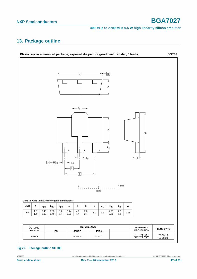
13. Package outline
Fig 27. Package outline SOT89
REFERENCESOUTLINEVERSION
EUROPEANPROJECTION ISSUE DATE
IEC JEDEC JEITA
DIMENSIONS (mm are the original dimensions)
SOT89 TO-243 SC-62 06-03-1606-08-29
w M
e1
e
EHE
B
B
0 2 4 mm
scale
bp3
bp2
bp1
c
D
Lp
A
Plastic surface-mounted package; exposed die pad for good heat transfer; 3 leads SOT89
1 2 3
UNIT A
mm1.61.4
0.480.35
c
0.440.23
D
4.64.4
E
2.62.4
HE Lp
4.253.75
e
3.0
w
0.13
e1
1.51.20.8
bp2bp1
0.530.40
bp3
1.81.4
BGA7027 All information provided in this document is subject to legal disclaimers. © NXP B.V. 2010. All rights reserved.
Product data sheet Rev. 2 — 26 November 2010 17 of 21
NXP Semiconductors BGA7027400 MHz to 2700 MHz 0.5 W high linearity silicon amplifier
14. Abbreviations
15. Revision history
Table 14. Abbreviations
Acronym Description
3GPP 3rd Generation Partnership Project
CPE Customer-Premises Equipment
DPCH Dedicated Physical CHannel
ESD ElectroStatic Discharge
HTOL High Temperature Operating Life
IMD3 3rd-order InterModulation Distortion
ISM Industrial, Scientific and Medical
MMIC Monolithic Microwave Integrated Circuit
MoCA Multimedia over Coax Alliance
RFID Radio Frequency IDentification
W-CDMA Wideband Code Division Multiple Access
W-LAN Wireless Local Area Network
Table 15. Revision history
Document ID Release date Data sheet status Change notice Supersedes
BGA7027 v.2 20101126 Product data sheet - BGA7027 v.1
Modifications: • The status of this data sheet has been changed to Product data sheet
• Table 1 on page 1: some values have been changed
• Table 1 on page 1: some values have been added
• Table 4 on page 3: data for Pi(RF) have been added
• Table 5 on page 3: conditions have been changed
• Table 7 on page 3: some values have been changed
• Table 7 on page 3: some values have been added
• Figure 7 on page 7: figure has been added
• Figure 8 on page 7: figure has been added
• Figure 9 on page 8: figure has been added
• Figure 22 on page 14: figure has been added
• Figure 23 on page 14: figure has been added
• Figure 24 on page 14: figure has been added
BGA7027 v.1 20100811 Preliminary data sheet - -
BGA7027 All information provided in this document is subject to legal disclaimers. © NXP B.V. 2010. All rights reserved.
Product data sheet Rev. 2 — 26 November 2010 18 of 21

NXP Semiconductors BGA7027400 MHz to 2700 MHz 0.5 W high linearity silicon amplifier
16. Legal information
16.1 Data sheet status
[1] Please consult the most recently issued document before initiating or completing a design.
[2] The term ‘short data sheet’ is explained in section “Definitions”.
[3] The product status of device(s) described in this document may have changed since this document was published and may differ in case of multiple devices. The latest product status information is available on the Internet at URL http://www.nxp.com.
16.2 Definitions
Draft — The document is a draft version only. The content is still under internal review and subject to formal approval, which may result in modifications or additions. NXP Semiconductors does not give any representations or warranties as to the accuracy or completeness of information included herein and shall have no liability for the consequences of use of such information.
Short data sheet — A short data sheet is an extract from a full data sheet with the same product type number(s) and title. A short data sheet is intended for quick reference only and should not be relied upon to contain detailed and full information. For detailed and full information see the relevant full data sheet, which is available on request via the local NXP Semiconductors sales office. In case of any inconsistency or conflict with the short data sheet, the full data sheet shall prevail.
Product specification — The information and data provided in a Product data sheet shall define the specification of the product as agreed between NXP Semiconductors and its customer, unless NXP Semiconductors and customer have explicitly agreed otherwise in writing. In no event however, shall an agreement be valid in which the NXP Semiconductors product is deemed to offer functions and qualities beyond those described in the Product data sheet.
16.3 Disclaimers
Limited warranty and liability — Information in this document is believed to be accurate and reliable. However, NXP Semiconductors does not give any representations or warranties, expressed or implied, as to the accuracy or completeness of such information and shall have no liability for the consequences of use of such information.
In no event shall NXP Semiconductors be liable for any indirect, incidental, punitive, special or consequential damages (including - without limitation - lost profits, lost savings, business interruption, costs related to the removal or replacement of any products or rework charges) whether or not such damages are based on tort (including negligence), warranty, breach of contract or any other legal theory.
Notwithstanding any damages that customer might incur for any reason whatsoever, NXP Semiconductors’ aggregate and cumulative liability towards customer for the products described herein shall be limited in accordance with the Terms and conditions of commercial sale of NXP Semiconductors.
Right to make changes — NXP Semiconductors reserves the right to make changes to information published in this document, including without limitation specifications and product descriptions, at any time and without notice. This document supersedes and replaces all information supplied prior to the publication hereof.
Suitability for use — NXP Semiconductors products are not designed, authorized or warranted to be suitable for use in life support, life-critical or safety-critical systems or equipment, nor in applications where failure or
malfunction of an NXP Semiconductors product can reasonably be expected to result in personal injury, death or severe property or environmental damage. NXP Semiconductors accepts no liability for inclusion and/or use of NXP Semiconductors products in such equipment or applications and therefore such inclusion and/or use is at the customer’s own risk.
Applications — Applications that are described herein for any of these products are for illustrative purposes only. NXP Semiconductors makes no representation or warranty that such applications will be suitable for the specified use without further testing or modification.
Customers are responsible for the design and operation of their applications and products using NXP Semiconductors products, and NXP Semiconductors accepts no liability for any assistance with applications or customer product design. It is customer’s sole responsibility to determine whether the NXP Semiconductors product is suitable and fit for the customer’s applications and products planned, as well as for the planned application and use of customer’s third party customer(s). Customers should provide appropriate design and operating safeguards to minimize the risks associated with their applications and products.
NXP Semiconductors does not accept any liability related to any default, damage, costs or problem which is based on any weakness or default in the customer’s applications or products, or the application or use by customer’s third party customer(s). Customer is responsible for doing all necessary testing for the customer’s applications and products using NXP Semiconductors products in order to avoid a default of the applications and the products or of the application or use by customer’s third party customer(s). NXP does not accept any liability in this respect.
Limiting values — Stress above one or more limiting values (as defined in the Absolute Maximum Ratings System of IEC 60134) will cause permanent damage to the device. Limiting values are stress ratings only and (proper) operation of the device at these or any other conditions above those given in the Recommended operating conditions section (if present) or the Characteristics sections of this document is not warranted. Constant or repeated exposure to limiting values will permanently and irreversibly affect the quality and reliability of the device.
Terms and conditions of commercial sale — NXP Semiconductors products are sold subject to the general terms and conditions of commercial sale, as published at http://www.nxp.com/profile/terms, unless otherwise agreed in a valid written individual agreement. In case an individual agreement is concluded only the terms and conditions of the respective agreement shall apply. NXP Semiconductors hereby expressly objects to applying the customer’s general terms and conditions with regard to the purchase of NXP Semiconductors products by customer.
No offer to sell or license — Nothing in this document may be interpreted or construed as an offer to sell products that is open for acceptance or the grant, conveyance or implication of any license under any copyrights, patents or other industrial or intellectual property rights.
Export control — This document as well as the item(s) described herein may be subject to export control regulations. Export might require a prior authorization from national authorities.
Document status[1][2] Product status[3] Definition
Objective [short] data sheet Development This document contains data from the objective specification for product development.
Preliminary [short] data sheet Qualification This document contains data from the preliminary specification.
Product [short] data sheet Production This document contains the product specification.
BGA7027 All information provided in this document is subject to legal disclaimers. © NXP B.V. 2010. All rights reserved.
Product data sheet Rev. 2 — 26 November 2010 19 of 21
NXP Semiconductors BGA7027400 MHz to 2700 MHz 0.5 W high linearity silicon amplifier
Non-automotive qualified products — Unless this data sheet expressly states that this specific NXP Semiconductors product is automotive qualified, the product is not suitable for automotive use. It is neither qualified nor tested in accordance with automotive testing or application requirements. NXP Semiconductors accepts no liability for inclusion and/or use of non-automotive qualified products in automotive equipment or applications.
In the event that customer uses the product for design-in and use in automotive applications to automotive specifications and standards, customer (a) shall use the product without NXP Semiconductors’ warranty of the product for such automotive applications, use and specifications, and (b) whenever customer uses the product for automotive applications beyond NXP Semiconductors’ specifications such use shall be solely at customer’s own risk, and (c) customer fully indemnifies NXP Semiconductors for any
liability, damages or failed product claims resulting from customer design and use of the product for automotive applications beyond NXP Semiconductors’ standard warranty and NXP Semiconductors’ product specifications.
Quick reference data — The Quick reference data is an extract of the product data given in the Limiting values and Characteristics sections of this document, and as such is not complete, exhaustive or legally binding.
16.4 TrademarksNotice: All referenced brands, product names, service names and trademarks are the property of their respective owners.
17. Contact information
For more information, please visit: http://www.nxp.com
For sales office addresses, please send an email to: [email protected]
BGA7027 All information provided in this document is subject to legal disclaimers. © NXP B.V. 2010. All rights reserved.
Product data sheet Rev. 2 — 26 November 2010 20 of 21

NXP Semiconductors BGA7027400 MHz to 2700 MHz 0.5 W high linearity silicon amplifier
18. Contents
1 Product profile . . . . . . . . . . . . . . . . . . . . . . . . . . 11.1 General description . . . . . . . . . . . . . . . . . . . . . 11.2 Features and benefits . . . . . . . . . . . . . . . . . . . . 11.3 Applications . . . . . . . . . . . . . . . . . . . . . . . . . . . 11.4 Quick reference data . . . . . . . . . . . . . . . . . . . . 1
2 Pinning information. . . . . . . . . . . . . . . . . . . . . . 2
3 Ordering information. . . . . . . . . . . . . . . . . . . . . 2
4 Functional diagram . . . . . . . . . . . . . . . . . . . . . . 2
5 Limiting values. . . . . . . . . . . . . . . . . . . . . . . . . . 3
6 Thermal characteristics . . . . . . . . . . . . . . . . . . 3
7 Static characteristics. . . . . . . . . . . . . . . . . . . . . 3
8 Dynamic characteristics . . . . . . . . . . . . . . . . . . 3
9 Scattering parameters . . . . . . . . . . . . . . . . . . . . 4
10 Reliability information . . . . . . . . . . . . . . . . . . . . 5
11 Moisture sensitivity . . . . . . . . . . . . . . . . . . . . . . 5
12 Application information. . . . . . . . . . . . . . . . . . . 612.1 920 MHz to 960 MHz . . . . . . . . . . . . . . . . . . . . 612.2 1930 MHz to 1990 MHz . . . . . . . . . . . . . . . . . 1012.3 2110 MHz to 2170 MHz . . . . . . . . . . . . . . . . . 1212.4 PCB stack . . . . . . . . . . . . . . . . . . . . . . . . . . . . 16
13 Package outline . . . . . . . . . . . . . . . . . . . . . . . . 17
14 Abbreviations. . . . . . . . . . . . . . . . . . . . . . . . . . 18
15 Revision history. . . . . . . . . . . . . . . . . . . . . . . . 18
16 Legal information. . . . . . . . . . . . . . . . . . . . . . . 1916.1 Data sheet status . . . . . . . . . . . . . . . . . . . . . . 1916.2 Definitions. . . . . . . . . . . . . . . . . . . . . . . . . . . . 1916.3 Disclaimers . . . . . . . . . . . . . . . . . . . . . . . . . . . 1916.4 Trademarks. . . . . . . . . . . . . . . . . . . . . . . . . . . 20
17 Contact information. . . . . . . . . . . . . . . . . . . . . 20
18 Contents . . . . . . . . . . . . . . . . . . . . . . . . . . . . . . 21
© NXP B.V. 2010. All rights reserved.
For more information, please visit: http://www.nxp.comFor sales office addresses, please send an email to: [email protected]
Date of release: 26 November 2010
Document identifier: BGA7027
Please be aware that important notices concerning this document and the product(s)described herein, have been included in section ‘Legal information’.