beam test of a segmented foil sem grid -...
TRANSCRIPT
Fermilab-Pub-05-045-AD
Beam Test of a Segmented Foil SEM Grid
S.E. Kopp a,∗ D.Indurthy a Z.Pavlovich a M.Proga a R.Zwaska a
S.Childress b R.Ford b C.Kendziora b T.Kobilarcik b C.Moore b
G.Tassotto b
aDepartment of Physics, University of Texas, Austin, Texas 78712 USAbFermi National Accelerator Laboratory, Batavia, Illinois 60510 USA
Abstract
A prototype Secondary-electron Emission Monitor (SEM) was installed in the 8 GeVproton transport line for the MiniBooNE experiment at Fermilab. The SEM is asegmented grid made with 5 µm Ti foils, intended for use in the 120 GeV NuMIbeam at Fermilab. Similar to previous workers, we found that the full collection ofthe secondary electron signal requires a bias voltage to draw the ejected electronscleanly off the foils, and this effect is more pronounced at larger beam intensity. Thebeam centroid and width resolutions of the SEM were measured at beam widthsof 3, 7, and 8 mm, and compared to calculations. Extrapolating the data from thisbeam test, we expect a centroid and width resolutions of δxbeam = 20 µm andδσbeam = 25 µm, respectively, in the NuMI beam which has 1 mm spot size.
Key words: particle beam, instrumentation, secondary electron emissionPACS: 07.77Ka, 29.27Ac, 29.27Fh, 29.40.-n
1 Introduction
Beam profiles may be measured via the process of secondary electron emis-sion[1]. A secondary electron monitor (SEM) consists of a metal screen oflow work function from which low (<100 eV) energy electrons are ejected.While the probability for secondary electron emission is low (∼0.01/beamparticle), these devices can produce signals of 10-100nC when 4 × 10¹³ beam
∗ Corresponding author e-mail [email protected]
Preprint submitted to Elsevier Science 13 July 2005
HV
e
Beam Particle−e−e
HV Signal HVSignal
−e
−e−
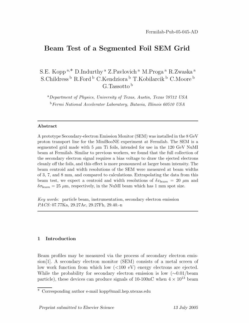
Fig. 1. Schematic of a segmented secondary emission monitor (SEM): electronsejected by the signal planes are drawn away by bias planes at a positive voltage.
particles per spill pass through the device, permitting their use as beam mon-itors[2]. Furthermore, the process of secondary electron emission is a surfacephenomenon[3], so that electron emitting foils or wires of very thin (1-10 µm)dimensions may be used without penalty to the signal size[4]. Often a posi-tive voltage on a nearby foil (”clearing field”) is used to draw the secondaryelectrons cleanly away from the signal screen. A schematic SEM is shown inFigure 1.
Secondary electron emission monitors have replaced ionization chambers asbeam monitors for over 40 years[2]. An ionization chamber monitors beam in-tensity by measuring the ionized charge in a gas volume collected on a chamberelectrode. Such a device places a large amount of material (∼ 10−2−10−3 λint)in the beam which results in emittance blowup and beam loss, both of whichare unacceptable in high intensity beams. A further limitation of ionizationchambers is that space charge buildup limits them to measurements of beamswith intenstities of < 1016 particles/cm2/sec[5], nearly 5 orders of magnitudebelow requirements of present extracted beamlines. SEM’s, in contrast, areextremely linear in response [2,6], and the prototype SEM discussed in thisnote is 7 × 10⁻⁶ interaction lengths thick.
For the NuMI beam [7], we desire a segmented SEM which measures thebeam intensity, the beam centroid position, and the beam’s lateral profile.The beam spot is anticipated to be ∼1mm. The required SEM segmentationis of order 1mm. The two SEM’s near the NuMI target require segmentationof 0.5mm in order to specify the beam position and angle onto the target atthe 50 µrad level. The segmented SEM will measure profile out to 22 mmin the horizontal and vertical. A single, large foil will cover the remainingaperture out to 50 mm radius in order to measure any potential beam halo.Additional thin foil SEM’s are envisaged for the 8 GeV transport line forthe MiniBooNE experiment [8] and for the transfer line between the 8 GeVBooster and 120 GeV Main Injector at FNAL.
2

A prototype SEM was tested in the 8 GeV beam transport line for the Mini-BooNE experiment in May 2003. While the MiniBooNE beam parametersdiffer from those anticipated for NuMI (see Table 1), this test permitted earlyverification of the foil SEM design. Some differences, listed in Table 1, existbetween the foils designed for the prototype and the final SEM chambers in-stalled in the NuMI line. Further details of the prototype design are given inSection 2, while the final SEM design description can be found in Ref [9].
During the beam tests, the SEM was used to measure beam position and sizeat one location in the MiniBooNE line. Because it was the only profile monitorin that portion of the transport line, no independent measurement existed tocorroborate the prototype’s beam size measurements. A pair of nearby capac-itative Beam Position Monitors (BPM’s) was able to corroborate the SEM’sbeam centroid measurement. The SEM’s expected beam centroid resolutionand beam width resolution are related, however, because both depend uponseveral aspects of the SEM design, such as readout noise and the positionaccuracy of the segmented SEM grid assembly. In this note, we analyze theSEM’s centroid and width resolution during the test in the MiniBooNE line.These measurements are compared to calculations of expected centroid reso-lution performance. Following the validation of the calculations using the testbeam data, we extrapolate the expected beam size resolution achievable fromthe SEM’s to the case for the narrow NuMI beam.
BEAM MiniBooNE NuMI
Proton energy (GeV) 8 120
Intensity (×1012 ppp) 5 40
Spill Rate (Hz) 5 0.5
Spill Duration (µs) 1.56 8.67
Horizontal beam size (mm) 6-8 1.0
Vertical beam size (mm) 3 1.0
SEM Prototype Final SEM
Strip width (mm) 0.75 0.15
Strip pitch (mm) 1 1
Foil thickness (µm) 5 5Table 1Comparison of MiniBooNE and NuMI beam lines and of the prototype and finaldesign SEM’s. Characteristics of the prototype that was tested in MiniBooNE beam-line along with the characteristics of the final design SEMs that are used in NuMIbeamline are listed.
3
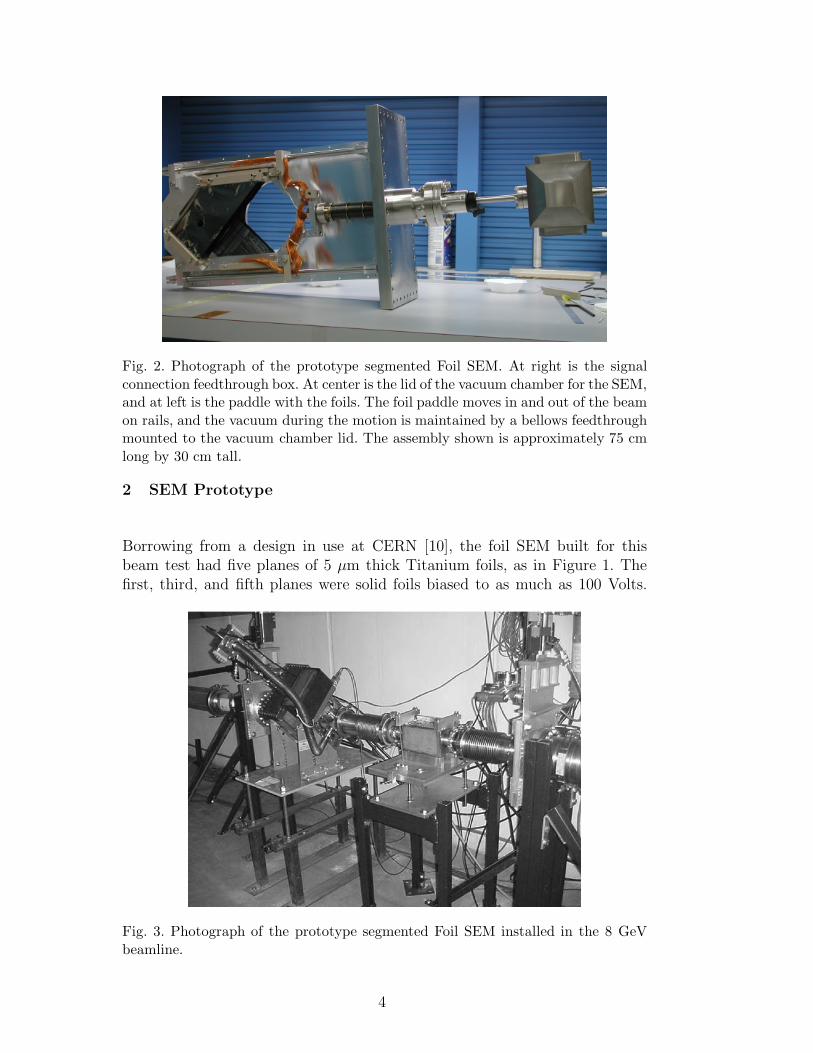
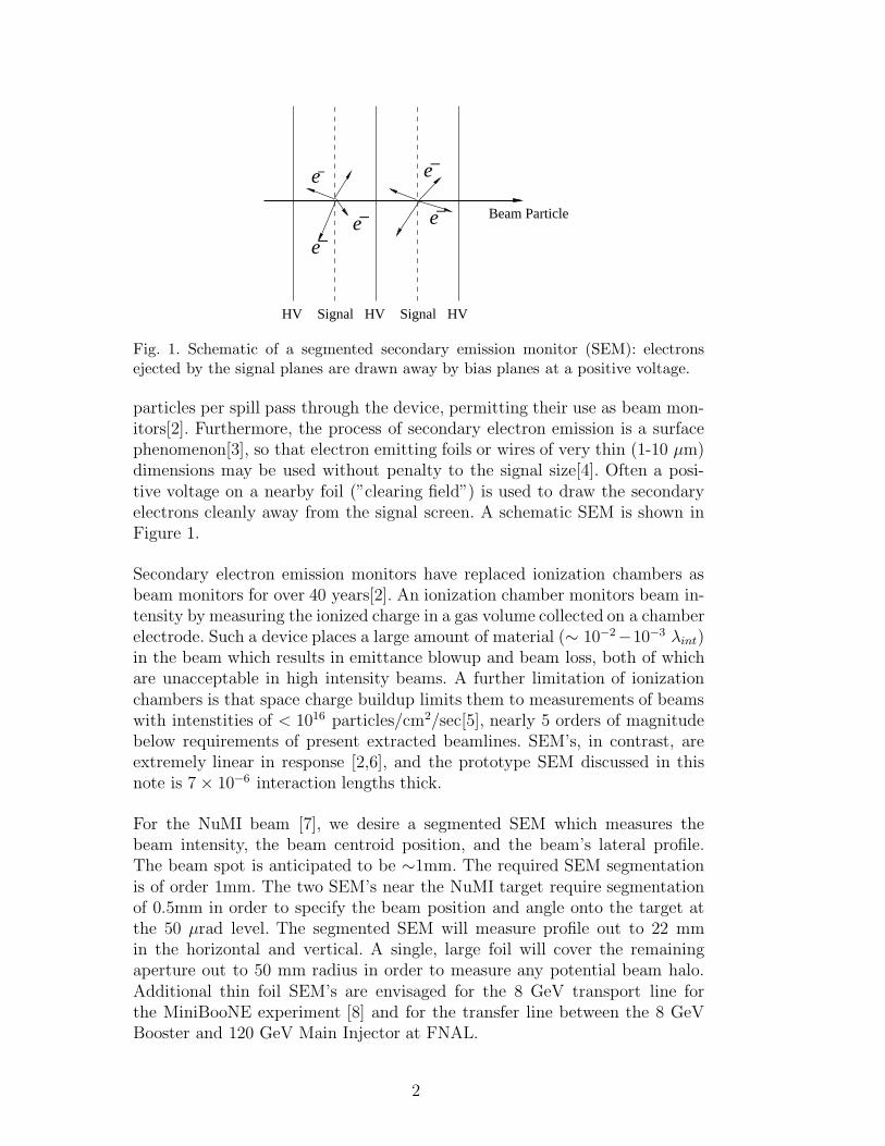
Fig. 2. Photograph of the prototype segmented Foil SEM. At right is the signalconnection feedthrough box. At center is the lid of the vacuum chamber for the SEM,and at left is the paddle with the foils. The foil paddle moves in and out of the beamon rails, and the vacuum during the motion is maintained by a bellows feedthroughmounted to the vacuum chamber lid. The assembly shown is approximately 75 cmlong by 30 cm tall.
2 SEM Prototype
Borrowing from a design in use at CERN [10], the foil SEM built for thisbeam test had five planes of 5 µm thick Titanium foils, as in Figure 1. Thefirst, third, and fifth planes were solid foils biased to as much as 100 Volts.
Fig. 3. Photograph of the prototype segmented Foil SEM installed in the 8 GeVbeamline.
4

8711
VT
871
8693
8691
8692
Tor
860
������������
HT
870 U
T S
EM
870A
870B
�������
�������
VP8
71
VT
869
VP8
70
HP8
70
871B
871A
Fig. 4. Beamline segment around SEM prototype. Tor = beam current toroid, HPand VP = horizontal and vertical beam position monitor (BPM), HT and VT = hor-izontal and vertical trim magnets, UT SEM = University of Texas foil SEM.
Planes 2 and 4 were segmented at 1 mm pitch (0.75 mm wide strips with0.25 mm gaps between adjacent strips). The strips were mounted on ceramiccombs with rectangular grooves which mechancally held the strips and alignedthem onto the grid. Each strip had an accordion-like spring to tension it andcompensate for beam heating. The foil strips for the prototype were quite long,ranging from 15-25 cm in length. Each strip was read out separately into acharge-integrating circuit[11] gated around the beam spill.
A new aspect of the present SEM design is that the foils were mounted ona frame which does not traverse the beam as the SEM is inserted into or re-tracted from the beam. The segmented foils are mounted at ±45◦ to provideboth horizontal and vertical beam profiles, and these are mounted on a hexag-onal frame which encloses the beam at all times, leaving a clear space whenit is desired to retract the foils away from the beam, as shown in Figure 2.The signals from the foils are routed through a vacuum bellows feedthroughvia kapton-insulated cables to a signal feedthrough box shown at the right ofthe photo. While the final NuMI SEM chambers have stepper motor-drivenactuators [9] to move the foils into or out of the beam, the prototype requiredmanual manipulation of the bellows feedthrough to insert the foil paddle. Aphotograph of the SEM, mounted in its rectangular vacuum chamber andinstalled in the 8 GeV transport line, is shown in Figure 3.
The use of Titanium as the active medium was motivated by the loss of Sec-ondary Electron Emission (SEE) signal from other materials after prolongedexposure in the beam [12–15]. For beam nominally on center through a longrun, such signal loss results in degraded beam centroid magnitude and alsoresults in artificially enhanced beam tails, since the beam tails irradiate theSEM to a lesser extent. Titanium suffers less from the loss of SEE signal, evenfor relatively simple cleaning and handling procedures for the foils [15].
5
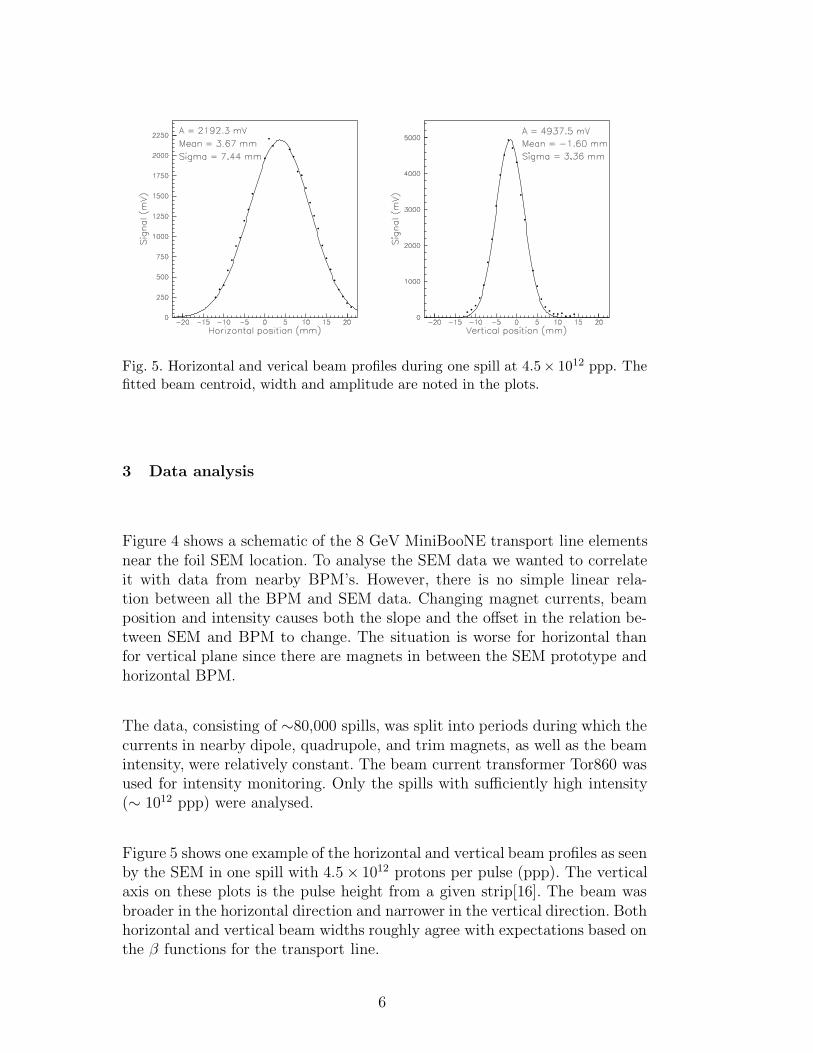
Fig. 5. Horizontal and verical beam profiles during one spill at 4.5× 10¹² ppp. Thefitted beam centroid, width and amplitude are noted in the plots.
3 Data analysis
Figure 4 shows a schematic of the 8 GeV MiniBooNE transport line elementsnear the foil SEM location. To analyse the SEM data we wanted to correlateit with data from nearby BPM’s. However, there is no simple linear rela-tion between all the BPM and SEM data. Changing magnet currents, beamposition and intensity causes both the slope and the offset in the relation be-tween SEM and BPM to change. The situation is worse for horizontal thanfor vertical plane since there are magnets in between the SEM prototype andhorizontal BPM.
The data, consisting of ∼80,000 spills, was split into periods during which thecurrents in nearby dipole, quadrupole, and trim magnets, as well as the beamintensity, were relatively constant. The beam current transformer Tor860 wasused for intensity monitoring. Only the spills with sufficiently high intensity(∼ 1012 ppp) were analysed.
Figure 5 shows one example of the horizontal and vertical beam profiles as seenby the SEM in one spill with 4.5 × 10¹² protons per pulse (ppp). The verticalaxis on these plots is the pulse height from a given strip[16]. The beam wasbroader in the horizontal direction and narrower in the vertical direction. Bothhorizontal and vertical beam widths roughly agree with expectations based onthe β functions for the transport line.
6

Fig. 6. (Normalized) total charge collected from the SEM summed over all 44 strips,plotted as a function of the applied bias voltage. The data were taken at severalbeam intensities, ranging from 4×10¹¹ protons/pulse to 4×10¹² protons/pulse.
4 Bias Voltage Study
The voltage applied to the SEM’s bias foils was typically 100 Volts, greaterthan the typical 20-30 eV kinetic energy of secondary electrons emitted froma foil surface.[1] To understand the effect of the bias voltage on the signalcollection efficiency, we accumulated data at several fixed beam intensitiesvarying from 4×10¹¹ protons/pulse (ppp) to 4×10¹² ppp. During each periodof fixed beam intensity, the voltage applied to the bias foils was varied andthe total charge collected from all the signal strips measured. The results areplotted in Figure 6. The signal collected from the SEM is normalized to 100%efficiency by dividing by the signal collected at 4 × 10¹² ppp and 100 Volts.Both the horizontal and vertical signal foils agree within 1.5%. As can beseen, applying a voltage increases the efficiency, as has been noted by others[12,17]. Also, our data suggest that the required applied voltage to achieve100% efficiency increases as the beam intensity increases. The magnitude ofthis effect may reflect surface impurities on the foils or be caused by therelatively poor vacuum in this chamber, which was several 10−7 Torr duringthe test.
7

Fig. 7. (left) The correlation between positions measured by the vertical BPM andthose measured by the SEM. (right) The residuals from the best fit line. From theresiduals we can infer that the sum in quadrature of BPM and SEM resolutions is127µm.
5 Measured SEM Centroid Resolution
The centroid resolution of the SEM depends upon the width of the beam, theintensity of the beam, and upon the electronics readout noise on the SEMchannels. The beam width in vertical direction was nearly constant at σx =3.4 mm, while the horizontal beam size varied between σy = 7.4 mm andσy = 8.2 mm, during the test period. This gives us 3 different beam widthsfor which we try to find the SEM centroid resolution.
To find the beam centroid resolution in the vertical plane we correlate itsreported beam position with that of the BPM labelled VP871. Figure 7 showsthe BPM data ploted versus SEM data over a range of spills in which thebeam was observed to move substantially across the chambers. The residualsof the data from the best fit line are also shown in a figure, and show an RMSof 127 µm. The residuals should be a measure of the two devices’ resolutions,added in quadrature:
√σ2
SEM + (ασBPM)2 = 127 µm. (1)
where σSEM and σBPM are the intrinsic resolutions of the detectors, and α =1.1 is a scale factor between the SEM and BPM which is taken from the slopeof the line in Figure 7. This scale factor can result from either optics of thetransport line or miscalibrations between the SEM and BPM.
In order to separate the individual BPM and SEM resolutions, we select adifferent time span of spills in which the beam position at the detectors was
8
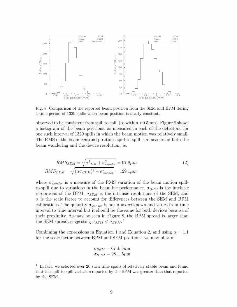
Fig. 8. Comparison of the reported beam position from the SEM and BPM duringa time period of 1329 spills when beam position is nearly constant.
observed to be consistent from spill to spill (to within <0.5mm). Figure 8 showsa histogram of the beam positions, as measured in each of the detectors, forone such interval of 1329 spills in which the beam motion was relatively small.The RMS of the beam centroid positions spill-to-spill is a measure of both thebeam wandering and the device resolution, ie.
RMSSEM =√
σ2SEM + σ2
wander = 97.8µm (2)
RMSBPM =√
(ασBPM)2 + σ2wander = 129.1µm
where σwander is a measure of the RMS variation of the beam motion spill-to-spill due to variations in the beamline performance, σBPM is the intrinsicresolutions of the BPM, σSEM is the intrinsic resolutions of the SEM, andα is the scale factor to account for differences between the SEM and BPMcalibrations. The quantity σwander is not a priori known and varies from timeinterval to time interval but it should be the same for both devices because oftheir proximity. As may be seen in Figure 8, the BPM spread is larger thanthe SEM spread, suggesting σSEM < σBPM. 1
Combining the expressions in Equation 1 and Equation 2, and using α = 1.1for the scale factor between BPM and SEM positions, we may obtain:
σSEM = 67 ± 5µmσBPM = 98 ± 5µm
1 In fact, we selected over 20 such time spans of relatively stable beam and foundthat the spill-to-spill variation reported by the BPM was greater than that reportedby the SEM.
9

We have repeated this analysis of the vertical beam data for several timeintervals. The resolutions are observed to vary by an RMS of 5 µm, with thevariation possibly due to beam-related effects or variation in resolution acrossthe aperture of the SEM or BPM.
In the horizontal view the presence of the focusing quadrupoles 870A and870B, as well as the trim magnet HT870, complicates direct comparison of thebeam position reported by the prototype SEM and the nearby horizontal BPMlabelled HP870. Furthermore, the beam width varied between 7.4 mm and 8.2mm, and was correlated with two different beam intensities. The expectedSEM centroid resolution is quite different for those two beam widths, so wesplit data into two sets. We looked at 32 intervals with 1000 spills each. Weassumed that the resolution for the horizontal BPM HP870 is the same asfor the identically-constructed vertical BPM VP871. In each time interval wecould find beam wandering (σwander) from the BPM measurements and thenplug that into SEM data and find σSEM . As a result we find:
σSEM (σx = 7.4mm) = 151 ± 5µmσSEM (σx = 8.2mm) = 171 ± 5µm
6 Expected SEM Resolution
The previous section measured the centroid resolution at three different beamwidths. A less reliable estimate was also made of the beam width resolution(see below). The beam centroid and width resolutions of a SEM grid areaffected by several instrumental factors[18]:
• The signal noise on each individual SEM strip (δyi).• The non-uniformity in strip spacing (δxi)• The number of SEM strips per beam σ
The first effect listed above smears the pulse height yi observed on an individ-
ual strip i by an amount δyi =√
δ2 + (εyi)2. The second effect, which arisesdue to the fact that the foil strips are not perfectly positioned on the grid,causes a smearing of the actual position xi of the strips. This form of stripplacement error we accounted for by assuming an additional uncertainty ofthe strip pulse heights of δyi = f ′(x) · δxi where f ′(x) is the derivative of thegaussian fitting function that we use to describe the beam profile and δxi isthe uncertainty in the strip positions.
We fit our beam test data to a model of expected beam centroid resolutionwhich incorporates the above effects. We simulated beam spills in a 44-channeldetector whose signals were smeared to account for electronics noise and foil
10
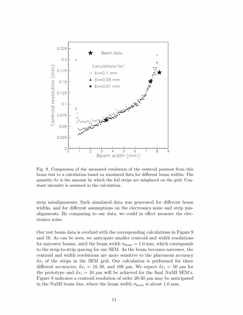
Fig. 9. Comparison of the measured resolution of the centroid position from thisbeam test to a calculation based on simulated data for different beam widths. Thequantity δx is the amount by which the foil strips are misplaced on the grid. Con-stant intensity is assumed in the calculation.
strip misalignments. Such simulated data was generated for different beamwidths, and for different assumptions on the electronics noise and strip mis-alignments. By comparing to our data, we could in effect measure the elec-tronics noise.
Our test beam data is overlaid with the corresponding calculations in Figure 9and 10. As can be seen, we anticipate smaller centroid and width resolutionsfor narrower beams, until the beam width σbeam = 1.0 mm, which correspondsto the strip-to-strip spacing for our SEM. As the beam becomes narrower, thecentroid and width resolutions are more sensitive to the placement accuracyδxi of the strips in the SEM grid. Our calculation is performed for threedifferent accuracies, δxi = 10, 50, and 100 µm. We expect δxi = 50 µm forthe prototype and δxi = 10 µm will be achieved for the final NuMI SEM’s.Figure 9 indicates a centroid resolution of order 20-30 µm may be anticipatedin the NuMI beam line, where the beam width σbeam is about 1.0 mm.
11

Fig. 10. Comparison of the measured resolution of the beam width from this beamtest to a calculation based on simulated data for different beam widths. The quantityδx is the amount by which the foil strips are misplaced on the grid. Constantintensity is assumed in the calculation.
We have also tried to understand the expected resolution of the beam widthmeasured by the SEM grid. Figure 10 shows the expected resolution of thebeam width as a function of the beam width. Overlaid on the plot in Figure 10are two points derived from the MiniBooNE test beam run which are thevariation of the width in the vertical plane as observed over two ranges ofbeam spills. A similar procedure was not possible in the horizontal, as thebeam width was observed to vary dramatically at high beam intensity to toemittance variation from the 8 GeV Booster accelerator, an effect confirmedby other instrumentation in the transport line.
7 Conclusion
From the prototype data we observe that the beam centroid resolution ofthe 1 mm pitch SEM prototype is around 64 ± 5 µm for the beam with
12
σ = 3.5 mm. From the extrapolation in Figure 9 to beam widths relevantfor NuMI, we anticipate a centroid resolution of 20-25 µm for a 1 mm beam.Although the beam intensity will be a factor of 5 larger in the NuMI beam,which might be expected to improve the SEM resolution due to increasedsignal size, this signal increase will be compensated by a signal decrease arisingfrom the narrower foil strip size in the NuMI SEM’s. Thus, the extrapolationshown in Figures 9 and 10 should be approximately correct.
The two SEM’s just upstream of the NuMI target will have finer pitch than theprototype SEM (0.5 mm compared to 1.0 mm), and also wider strips (0.25mmas compared to the 0.15mm of the transport line SEM’s). One therefore expectsthat (a) the mechanical assembly details of the 0.5mm SEM’s shall not be ascritical, since the beam size will be larger than the strip spacing, and (b) thepulse height smearing will not as greatly affect their resolutions because thewider strips will yield a 1.7 times greater signal. The results of the presentstudy suggest that these 0.5 mm SEM’s should behave in a 1.0 mm beammuch like the 1.0 mm prototype performance for a 2.0 mm beam. That is,an approximate scaling relation should exist between the strip pitch and thebeam width.
8 Acknowledgements
We thank Gianfranco Ferioli of CERN for extensive advice and consultationon segmented SEM’s and for sharing his designs, upon which the presentprototype is based. The beam test described in this memo was performedthanks to the efforts of members of the FNAL Particle Physics and AcceleratorDivisions as well as the University of Texas Department of Physics MechanicalSupport Shops. This work was supported by the U.S. Department of Energyunder contracts DE-FG03-93ER40757 and DE-AC02-76CH3000, and by theFondren Family Foundation.
References
[1] H. Bruining, Physics and Applications of Secondary Electron Emission,(London: Pergammon Press, 1954), pp. 3-7.
[2] G.W. Tautfest and H. R. Fechter, Rev. Sci. Instr. 26, 229 (1955).
[3] See, for example, E.J. Sternglass, Phys. Rev. 108, 1 (1957); B. Planskoy, Nucl.Instr. Meth. 24, 172 (1963); D. Harting, J.C. Kluyver and A. Kusumegi, CERN60-17 (1960); J.A. Blankenburg Nucl. Instr. Meth. 39, 303 (1966).
[4] R. Anne et al., Nucl. Instr. Meth. 152, 395 (1978).
13

[5] See, for example, R. Zwaska et al., ”Beam Tests of Ionization Chambers for theNuMI Neutrino Beam,” IEEE Trans. Nucl. Sci. 50: 1129-1135 (2003).
[6] S.I. Taimuty and B.S. Deaver, Rev. Sci. Instr. 32, 1098 (1961).
[7] See, for example, S. Kopp, ”The NuMI Beam at Fermilab,” Fermilab-Conf-04-0300 (Nov. 2004), also published in Proceedings of the 33rd ICFA AdvancedBeam Dynamics Workshop: High Intensity High Brightness Hadron Beams(ICFA HB2004), Bensheim, Darmstadt, Germany, 18-22 Oct 2004.
[8] C. Moore et al, Proc. of the 2003 Particle Accel. Conf., pp.1652-1654, Stanford,CA, May 3003.
[9] D. Indurthy et al, “Profile Monitor SEM’s for the NuMI Beam atFNAL”, Proceedings of the 11th International Beam Instrumentation Workshop(BIW04), AIP Conference Proc. 732, pg 341-349 (2004), Fermilab-Conf-04-520-AD (2004).
[10] G. Ferioli, private communication.
[11] W. Kissel, B. Lublinsky and A. Frank, “New SWIC Scanner/ControllerSystem,” presented at the 1995 International Conference on Accelerator andLarge Experimental Physics Control Systems, 1996.
[12] D.B. Isabelle & P.H. Roy, Nucl. Instr. Meth. 20, 17 (1963).
[13] E.L. Garwin and N. Dean, Method of Stabilizing High Current SecondaryEmission Monitors, in Proc. Symp. on Beam Intensity Measurement, Daresbury,England, p 22-26, April 1968.
[14] V. Agoritsas and R.L. Witkover, IEEE Trans. Nucl. Sci. 26, 3355 (1979).
[15] G. Ferioli and R. Jung, CERN-SL-97-71(BI), published in Proceedings of BeamDiagnostics and Instrumentation for Particle Accelerators (DIPAC), Frascati(Rome), Italy, Oct. 12-14, 1997.
[16] The SEM pulse height is nominally a charge whose magnitude should be of ordera percent of primary beam charge traversing a foil strip. These pulse heightswere read out using charge-integrating amplifiers whose gain and charge-to-voltage conversion were not well known for our test. The lack of knowledge ofthis conversion factor is not important for our final results.
[17] S.A. Blankenburg, J.K. Cobb, and J.J. Murray, Nucl. Instr. Meth. 39, 303(1966).
[18] Mike Plum “Interceptive Beam Diagnostics-Signal Creation and MaterialsInteractions”, Proceedings of the 11th International Beam InstrumentationWorkshop (BIW04), AIP Conf. Proc. 732, pg 23-46, Knoxville, TN (2004).
14