bc620 / 627at time and frequency processorchiclassiccomp.org/.../bc620-627at_usersguide_revb.pdf ·...
TRANSCRIPT

bc620 / 627ATTime and Frequency
Processor
Revision B
User’s Guide
8500-0011
March, 2004
Artisan Technology Group - Quality Instrumentation ... Guaranteed | (888) 88-SOURCE | www.artisantg.com

COPYRIGHT NOTICE
Copyright 1997 Symmetricom, Inc. All Rights Reserved
This User's Guide is provided to assist the user in the operation and maintenance of the supplied equipment. It isrecognized that multiple copies may be required to support even a single unit, and for this reason, permission is herebygranted to reproduce the supplied User's Guide for the purpose stated above, provide that this notice is included as partof the copy. Additional copies are also available from Symmetricom Inc for a nominal fee.
In no case, however, does the supply of these User's Guide’s or the granting of rights to reproduce the User's Guide’s,grant any rights to use information contained within to reproduce the supplied equipment or software, either in whole orpart.
The equipment and software described in this User's Guide has been developed solely at the expense of SymmetricomInc and is proprietary. No unlimited rights in technical data are granted. Limited Rights as per DFARS 252.227-7013shall be effective for ten years from the copyright date.
FEDERAL COMMUNICATIONS COMMISSION (FCC) STATEMENT
This equipment is certified to comply with the limits for a Class A computing device pursuant to Part 15,Subpart B of FCC Rules.
This equipment generates and uses radio frequency (RF) energy. If not installed and used properly, that is, instrict accordance with the manufacturer's instructions, it may cause interference to radio or televisionreception.
If this equipment does cause interference to radio or television reception, which can be determined by turningthe equipment on and off, the user is encouraged to correct the interference by one or more of the followingmeasures:
• Reorient the radio/television receiving antenna. • Move the antenna leads away from any wire runs to the personal computer with the Symmetricom
module. • If using an indoor antenna, have a quality outdoor antenna installed. • Relocate the personal computer with respect to the radio/television receiver. • Connect the AC transformer to a different outlet so the personal computer and the radio/television are on
different branch circuits.
If necessary, the user should consult the dealer or an experienced radio/television technician for suggestionsor reference the following booklet, prepared by the Federal Communications Commission, helpful: How toIdentify and Resolve Radio-TV Interference Problems. This booklet is available from the U.S: GovernmentPrinting Office, Washington D.C. 20402. Stock No. 004--000-00345-4.
Properly shielded and grounded cables and connectors must be used for connection to peripherals in order tomeet FCC emission limits. Symmetricom Inc. is not responsible for any radio or television interferencecaused by using other than recommended cables or by unauthorized modifications to this equipment. It is theresponsibility of the user to correct such interference.
Artisan Technology Group - Quality Instrumentation ... Guaranteed | (888) 88-SOURCE | www.artisantg.com

Symmetricom, Inc. bc620/627AT Time and Frequency Processor i
bc620/627ATTIME AND FREQUENCY PROCESSOR
TABLE OF CONTENTSSECTION PAGE
CHAPTER ONEINTRODUCTION
1.0 General.................................................................................................................................. 1-11.1 Key Features ......................................................................................................................... 1-11.2 Physical and Functional Overview ....................................................................................... 1-21.3 Performance Specifications .................................................................................................. 1-4
1.3.1 Time Code Reader ................................................................................................. 1-41.3.2 Time Code Generator............................................................................................. 1-41.3.3 Bus Characteristics ................................................................................................ 1-41.3.4 Digital Inputs ......................................................................................................... 1-41.3.5 Digital Outputs....................................................................................................... 1-51.3.6 External 10 MHz Input .......................................................................................... 1-51.3.7 Environmental Specifications ................................................................................ 1-51.3.8 Digital Synchronization Signals ............................................................................ 1-5
CHAPTER TWOINSTALLATION AND SETUP
2.0 General.................................................................................................................................. 2-12.1 Base Address Selection......................................................................................................... 2-12.2 Installation Procedure ........................................................................................................... 2-42.3 Demonstration Programs ...................................................................................................... 2-52.4 MS-DOS Device Driver........................................................................................................ 2-5
CHAPTER THREESOFTWARE INTERFACE
3.0 General.................................................................................................................................. 3-1 3.0.1 Glossary of Key Terms .......................................................................................... 3-13.1 Registers................................................................................................................................ 3-2 3.1.1 PAGE Select Register ............................................................................................ 3-2 3.1.2 TIMEREQ and TIME0-TIME7 Registers ............................................................. 3-2
3.1.3 CR0 Control Register 0 ......................................................................................... 3-83.1.4 EVENT0-EVENT8 Time Capture Registers ......................................................... 3-8
3.1.5 UNLOCK Register................................................................................................. 3-8
Artisan Technology Group - Quality Instrumentation ... Guaranteed | (888) 88-SOURCE | www.artisantg.com

TABLE OF CONTENTS
ii bc620/627AT Time and Frequency Processor Symmetricom, Inc.
3.1.6 ACK Register......................................................................................................... 3-8 3.1.7 Mask Interrupt MASK Register........................................................................... 3-10
3.1.8 INTSTAT Interrupt Status Register..................................................................... 3-103.1.9 FIFO Register ...................................................................................................... 3-113.1.10 STROBE2-STROBE6 Time Coincident Strobe Registers ................................ 3-11
3.2 Functional Description........................................................................................................ 3-113.2.1 Changing the Active Page.................................................................................... 3-11
3.2.2 Reading Time on Demand ................................................................................... 3-11 3.2.3 Event Time Capture ............................................................................................ 3-11 3.2.3.1 External Event Input ............................................................................ 3-12 3.2.3.2 Programmable Periodic Output............................................................. 3-12 3.2.3.3 Time Capture Lockout ......................................................................... 3-12 3.2.4 Time Coincidence Strobe Output ........................................................................ 3-12 3.2.5 FIFO Interface - Programming the bc620AT ...................................................... 3-133.3 PC AT Interrupts................................................................................................................. 3-13
CHAPTER FOURFIFO DATA PACKETS
4.0 General.................................................................................................................................. 4-14.1 Writing Data Packets ............................................................................................................ 4-1
4.1.1 Packet “A” - Select Operational Mode ................................................................ 4-1 4.1.2 Packet “B” - Set Major Time............................................................................... 4-2 4.1.3 Packet “C” - Command Input .............................................................................. 4-4 4.1.4 Packet “D” - Load the D/A Converter ................................................................. 4-4 4.1.5 Packet “F” - Heartbeat (Periodics) Control ......................................................... 4-5 4.1.6 Packet “G” - Propagation Delay Offset Control .................................................. 4-7 4.1.7 Packet “H” - Set Time Code Format for Mode 0................................................. 4-8 4.1.8 Packet “I” - Clock Source Select ......................................................................... 4-9 4.1.9 Packet “J” - Send Data to the GPS Receiver ....................................................... 4-9 4.1.10 Packet “K” - Select Generator Code.................................................................. 4-9 4.1.11 Packet “L” - Set Real Time Clock ................................................................... 4-10 4.1.12 Packet “M” - Local Time Offset Select ........................................................... 4-10 4.1.13 Packet “O” - Request Data from the bc620AT................................................ 4-11 4.1.14 Packet “P” - Path Selection.............................................................................. 4-15 4.1.15 Packet “Q” - Set Disciplining Gain ................................................................. 4-16 4.1.16 Packet “R” - Generator Time Offset Select ..................................................... 4-16
Artisan Technology Group - Quality Instrumentation ... Guaranteed | (888) 88-SOURCE | www.artisantg.com
TABLE OF CONTENTS
Symmetricom, Inc. bc620/627AT Time and Frequency Processor iii
CHAPTER FIVEPROGRAMMING EXAMPLES
5.0 General.................................................................................................................................. 5-15.1 Reading Time on Demand .................................................................................................... 5-15.2 External Event Time Capture ............................................................................................... 5-25.3 Program Periodic Frequency of 1000 Hz............................................................................. 5-25.4 Set Mode 1 and the Major Time ........................................................................................... 5-25.5 Select Mode 0 (IRIG B) and Advance TFP 2.5 Milliseconds .............................................. 5-3
CHAPTER SIXINPUT AND OUTPUT SIGNALS
6.0 General.................................................................................................................................. 6-16.1 Connector I/O ...................................................................................................................... 6-16.2 Jumper Selections ................................................................................................................. 6-2
CHAPTER SEVENADJUSTMENTS
7.0 General.................................................................................................................................. 7-17.1 Time Code Phase Lock Loop Adjustment ............................................................................ 7-17.2 Time Code Output Amplitude Adjustment........................................................................... 7-2
APPENDIX AIRIG TIME CODE FORMAT
A.0 General ................................................................................................................................ A-1
Artisan Technology Group - Quality Instrumentation ... Guaranteed | (888) 88-SOURCE | www.artisantg.com

TABLE OF CONTENTS
iv bc620/627AT Time and Frequency Processor Symmetricom, Inc.
This Page Intentionally Left Blank
Artisan Technology Group - Quality Instrumentation ... Guaranteed | (888) 88-SOURCE | www.artisantg.com

Symmetricom Inc bc620/627AT Time and Frequency Processor 1-1
CHAPTER ONEINTRODUCTION
1.0 GENERAL
This bc620/627AT Time and Frequency Processor (TFP) User's Guide provides the followinginformation:
• Introduction and key feature description. • Installation and setup. • Detailed operation and programming interfaces. • Programming examples. • Input and output signals. 1.1 KEY FEATURES The bc620/627AT has been designed with the following key features: • Time on demand (days through microseconds) with zero latency. This feature is
implemented with hardware registers which latch the current time upon host request. • Event logging (days through 0.1 microseconds). This feature is implemented with a second
set of hardware registers. Time is captured on a positive or negative input edge or secondarybus time request.
• Four operational modes are supported. Modes are distinguished by the reference source.
Mode Source Of Synchronization 0 Time code - IRIG A, IRIG B, XR3, 2137, NASA36 (modulated or
DC). 1 Free running - on board 10 MHz oscillator (VCXO) used as
reference. 2 1 PPS - synchronizes to external one pulse per second. 3 RTC - uses on board battery backed real time clock IC. 4 GPS - uses Acutime GPS receiver as reference (bc627AT only).
Artisan Technology Group - Quality Instrumentation ... Guaranteed | (888) 88-SOURCE | www.artisantg.com
CHAPTER ONE
1-2 bc620/627AT Time and Frequency Processor Symmetricom, Inc.
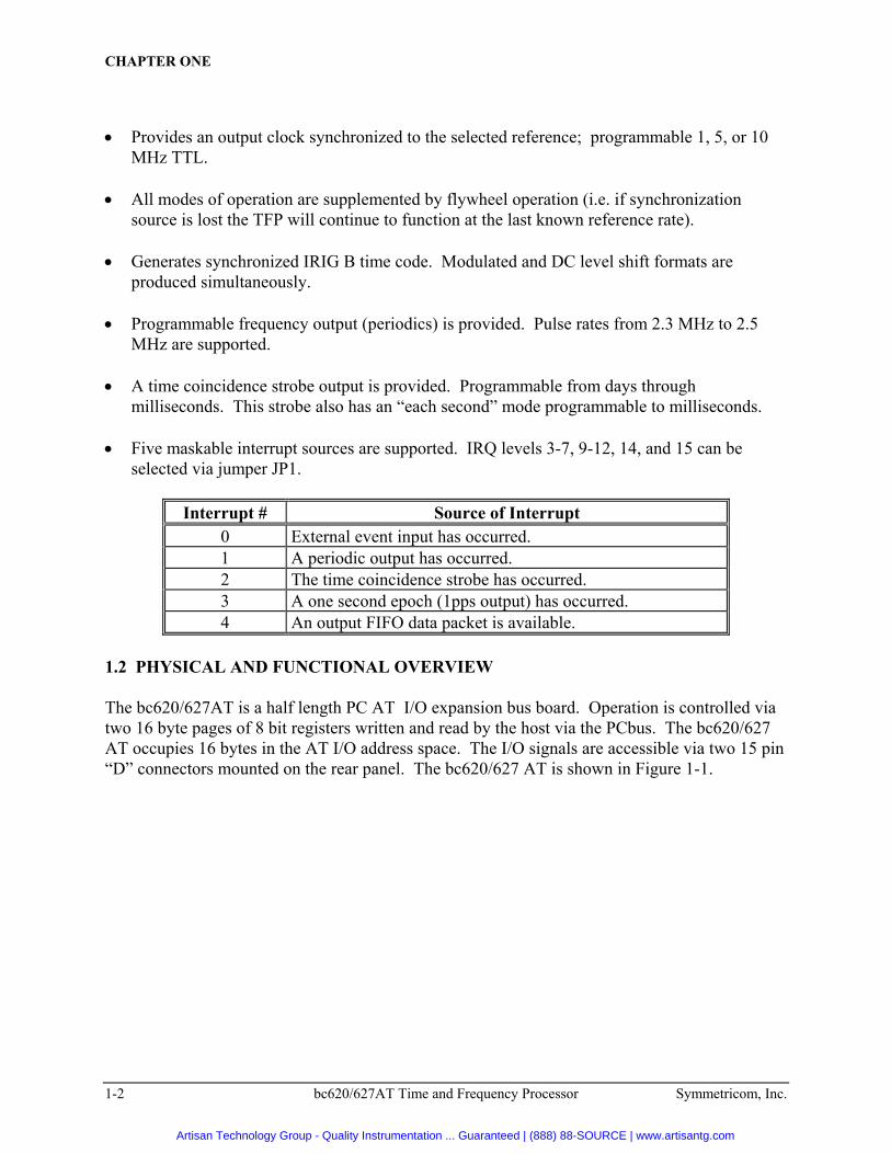
• Provides an output clock synchronized to the selected reference; programmable 1, 5, or 10
MHz TTL. • All modes of operation are supplemented by flywheel operation (i.e. if synchronization
source is lost the TFP will continue to function at the last known reference rate). • Generates synchronized IRIG B time code. Modulated and DC level shift formats are
produced simultaneously. • Programmable frequency output (periodics) is provided. Pulse rates from 2.3 MHz to 2.5
MHz are supported. • A time coincidence strobe output is provided. Programmable from days through
milliseconds. This strobe also has an “each second” mode programmable to milliseconds. • Five maskable interrupt sources are supported. IRQ levels 3-7, 9-12, 14, and 15 can be
selected via jumper JP1.
Interrupt # Source of Interrupt0 External event input has occurred.1 A periodic output has occurred.2 The time coincidence strobe has occurred.3 A one second epoch (1pps output) has occurred.4 An output FIFO data packet is available.
1.2 PHYSICAL AND FUNCTIONAL OVERVIEW
The bc620/627AT is a half length PC AT I/O expansion bus board. Operation is controlled viatwo 16 byte pages of 8 bit registers written and read by the host via the PCbus. The bc620/627AT occupies 16 bytes in the AT I/O address space. The I/O signals are accessible via two 15 pin“D” connectors mounted on the rear panel. The bc620/627 AT is shown in Figure 1-1.
Artisan Technology Group - Quality Instrumentation ... Guaranteed | (888) 88-SOURCE | www.artisantg.com

INTRODUCTION
Symmetricom, Inc. bc620/627AT Time and Frequency Processor 1-3
Figure 1-1bc620/627AT Time and Frequency Processor
Dat
um In
c, b
c620
AT
ASS
Y 1
1573
J
U1
C11
U8
C4
Y1
C15
U11
C13
U10
C12
U9
C50
R34
U3
C2C1
U2
U6
U5
C5
U12
RP1
C6C8R1
C51R35R2R3
+C10 R4 R5
R13
R7R14
R5
C7
U13
C17
C18
U7
C7
C9
U28
C52
U29
C53
C19
RV
1
RV
2
J3
U23
C39
U24
C41
R20
U25
Q1
Q2
R23R22R21
R25R24
C44+ +
B1
C28
U17
SW1
C21C20
C23C22
C25C24
U20
C30
U18
C20
R9
R8
R10
C31
U21
C37
C33
U19
C32
C34
C35
R12
R11
R15R16R17
U22
CR
1C
R2
R26
R27
R28
R29
R30
R31
2
4JP
2
R32
R33
U27
U26
C45
1357911131517192123
R15R14R12R11R10R9R7R6R5R4R3
JP1
OnIRQ
C43
+C
42
Y2
C40
SN
C46
+
C47
+
C49
+
J1
J2
TD1
C38R18R19
C48
U14
U15
U16
Q3
C27C28
C36
Artisan Technology Group - Quality Instrumentation ... Guaranteed | (888) 88-SOURCE | www.artisantg.com
CHAPTER ONE
1-4 bc620/627AT Time and Frequency Processor Symmetricom, Inc.
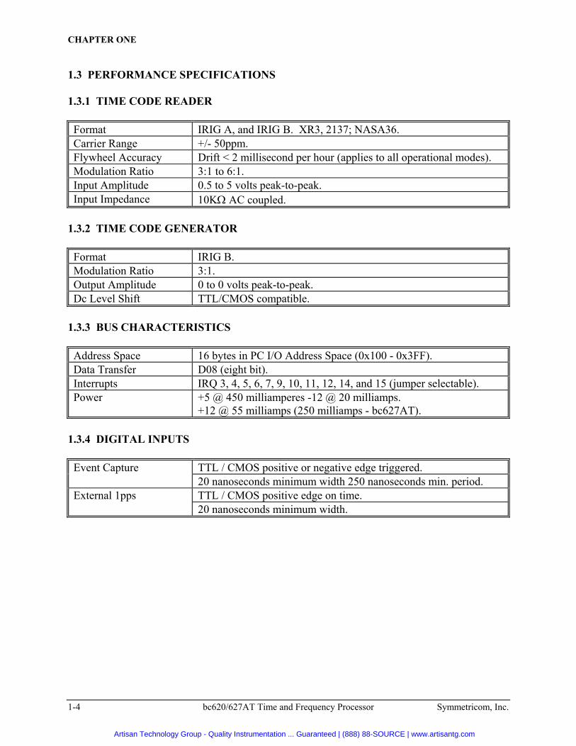
1.3 PERFORMANCE SPECIFICATIONS
1.3.1 TIME CODE READER
Format IRIG A, and IRIG B. XR3, 2137; NASA36.Carrier Range +/- 50ppm.Flywheel Accuracy Drift < 2 millisecond per hour (applies to all operational modes).Modulation Ratio 3:1 to 6:1.Input Amplitude 0.5 to 5 volts peak-to-peak.Input Impedance 10KΩ AC coupled.
1.3.2 TIME CODE GENERATOR
Format IRIG B.Modulation Ratio 3:1.Output Amplitude 0 to 0 volts peak-to-peak.Dc Level Shift TTL/CMOS compatible.
1.3.3 BUS CHARACTERISTICS
Address Space 16 bytes in PC I/O Address Space (0x100 - 0x3FF).Data Transfer D08 (eight bit).Interrupts IRQ 3, 4, 5, 6, 7, 9, 10, 11, 12, 14, and 15 (jumper selectable).Power +5 @ 450 milliamperes -12 @ 20 milliamps.
+12 @ 55 milliamps (250 milliamps - bc627AT).
1.3.4 DIGITAL INPUTS
Event Capture TTL / CMOS positive or negative edge triggered.20 nanoseconds minimum width 250 nanoseconds min. period.
External 1pps TTL / CMOS positive edge on time.20 nanoseconds minimum width.
Artisan Technology Group - Quality Instrumentation ... Guaranteed | (888) 88-SOURCE | www.artisantg.com
INTRODUCTION
Symmetricom, Inc. bc620/627AT Time and Frequency Processor 1-5
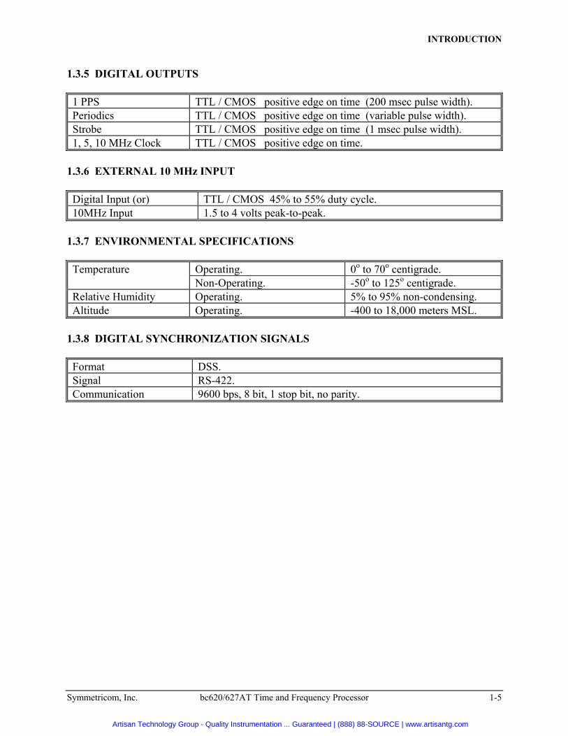
1.3.5 DIGITAL OUTPUTS
1 PPS TTL / CMOS positive edge on time (200 msec pulse width).Periodics TTL / CMOS positive edge on time (variable pulse width).Strobe TTL / CMOS positive edge on time (1 msec pulse width).1, 5, 10 MHz Clock TTL / CMOS positive edge on time.
1.3.6 EXTERNAL 10 MHz INPUT
Digital Input (or) TTL / CMOS 45% to 55% duty cycle.10MHz Input 1.5 to 4 volts peak-to-peak.
1.3.7 ENVIRONMENTAL SPECIFICATIONS
Temperature Operating. 0o to 70o centigrade.Non-Operating. -50o to 125o centigrade.
Relative Humidity Operating. 5% to 95% non-condensing.Altitude Operating. -400 to 18,000 meters MSL.
1.3.8 DIGITAL SYNCHRONIZATION SIGNALS
Format DSS.Signal RS-422.Communication 9600 bps, 8 bit, 1 stop bit, no parity.
Artisan Technology Group - Quality Instrumentation ... Guaranteed | (888) 88-SOURCE | www.artisantg.com

CHAPTER ONE
1-6 bc620/627AT Time and Frequency Processor Symmetricom, Inc.
This Page Intentionally Left Blank.
Artisan Technology Group - Quality Instrumentation ... Guaranteed | (888) 88-SOURCE | www.artisantg.com
CHAPTER TWO
2-2 bc620/627AT Time and Frequency Processor Symmetricom, Inc.
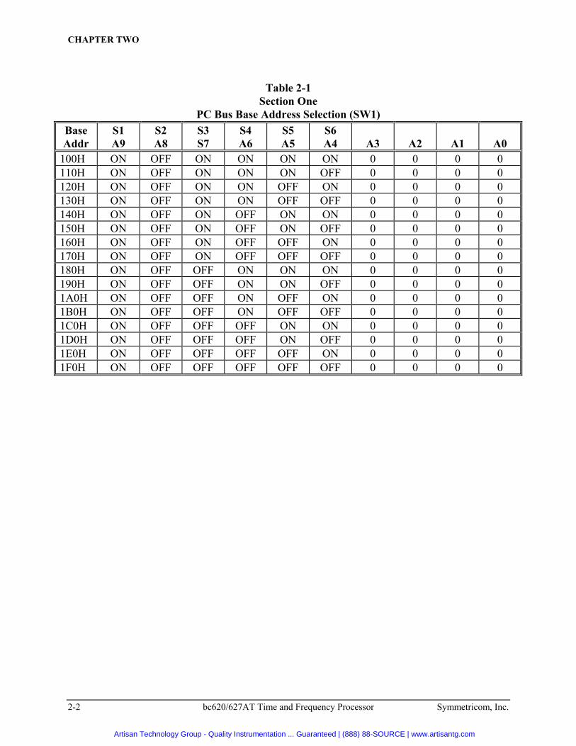
Table 2-1Section One
PC Bus Base Address Selection (SW1)BaseAddr
S1A9
S2A8
S3S7
S4A6
S5A5
S6A4 A3 A2 A1 A0
100H ON OFF ON ON ON ON 0 0 0 0110H ON OFF ON ON ON OFF 0 0 0 0120H ON OFF ON ON OFF ON 0 0 0 0130H ON OFF ON ON OFF OFF 0 0 0 0140H ON OFF ON OFF ON ON 0 0 0 0150H ON OFF ON OFF ON OFF 0 0 0 0160H ON OFF ON OFF OFF ON 0 0 0 0170H ON OFF ON OFF OFF OFF 0 0 0 0180H ON OFF OFF ON ON ON 0 0 0 0190H ON OFF OFF ON ON OFF 0 0 0 01A0H ON OFF OFF ON OFF ON 0 0 0 01B0H ON OFF OFF ON OFF OFF 0 0 0 01C0H ON OFF OFF OFF ON ON 0 0 0 01D0H ON OFF OFF OFF ON OFF 0 0 0 01E0H ON OFF OFF OFF OFF ON 0 0 0 01F0H ON OFF OFF OFF OFF OFF 0 0 0 0
Artisan Technology Group - Quality Instrumentation ... Guaranteed | (888) 88-SOURCE | www.artisantg.com
INSTALLATION AND SETUP
Symmetricom, Inc. bc620/627AT Time and Frequency Processor 2-3
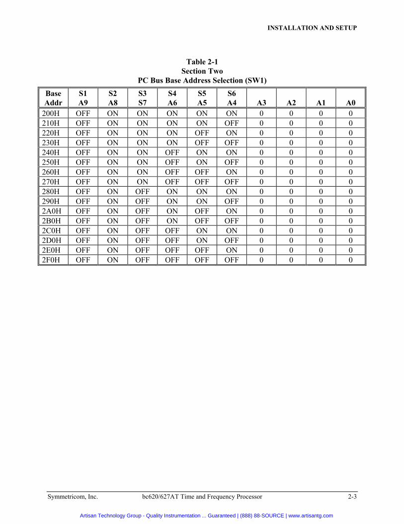
Table 2-1Section Two
PC Bus Base Address Selection (SW1)
BaseAddr
S1A9
S2A8
S3S7
S4A6
S5A5
S6A4 A3 A2 A1 A0
200H OFF ON ON ON ON ON 0 0 0 0210H OFF ON ON ON ON OFF 0 0 0 0220H OFF ON ON ON OFF ON 0 0 0 0230H OFF ON ON ON OFF OFF 0 0 0 0240H OFF ON ON OFF ON ON 0 0 0 0250H OFF ON ON OFF ON OFF 0 0 0 0260H OFF ON ON OFF OFF ON 0 0 0 0270H OFF ON ON OFF OFF OFF 0 0 0 0280H OFF ON OFF ON ON ON 0 0 0 0290H OFF ON OFF ON ON OFF 0 0 0 02A0H OFF ON OFF ON OFF ON 0 0 0 02B0H OFF ON OFF ON OFF OFF 0 0 0 02C0H OFF ON OFF OFF ON ON 0 0 0 02D0H OFF ON OFF OFF ON OFF 0 0 0 02E0H OFF ON OFF OFF OFF ON 0 0 0 02F0H OFF ON OFF OFF OFF OFF 0 0 0 0
Artisan Technology Group - Quality Instrumentation ... Guaranteed | (888) 88-SOURCE | www.artisantg.com
CHAPTER TWO
2-4 bc620/627AT Time and Frequency Processor Symmetricom, Inc.
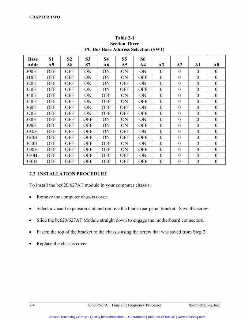
Table 2-1Section Three
PC Bus Base Address Selection (SW1)
2.2 INSTALLATION PROCEDURE
To install the bc620/627AT module in your computer chassis:
• Remove the computer chassis cover. • Select a vacant expansion slot and remove the blank rear panel bracket. Save the screw. • Slide the bc620/627AT Module straight down to engage the motherboard connectors. • Fasten the top of the bracket to the chassis using the screw that was saved from Step 2. • Replace the chassis cover.
BaseAddr
S1A9
S2A8
S3S7
S4A6
S5A5
S6A4 A3 A2 A1 A0
300H OFF OFF ON ON ON ON 0 0 0 0310H OFF OFF ON ON ON OFF 0 0 0 0320H OFF OFF ON ON OFF ON 0 0 0 0330H OFF OFF ON ON OFF OFF 0 0 0 0340H OFF OFF ON OFF ON ON 0 0 0 0350H OFF OFF ON OFF ON OFF 0 0 0 0360H OFF OFF ON OFF OFF ON 0 0 0 0370H OFF OFF ON OFF OFF OFF 0 0 0 0380H OFF OFF OFF ON ON ON 0 0 0 0390H OFF OFF OFF ON ON OFF 0 0 0 03A0H OFF OFF OFF ON OFF ON 0 0 0 03B0H OFF OFF OFF ON OFF OFF 0 0 0 03C0H OFF OFF OFF OFF ON ON 0 0 0 03D0H OFF OFF OFF OFF ON OFF 0 0 0 03E0H OFF OFF OFF OFF OFF ON 0 0 0 03F0H OFF OFF OFF OFF OFF OFF 0 0 0 0
Artisan Technology Group - Quality Instrumentation ... Guaranteed | (888) 88-SOURCE | www.artisantg.com
INSTALLATION AND SETUP
Symmetricom, Inc. bc620/627AT Time and Frequency Processor 2-5
2.3 DEMONSTRATION PROGRAMS
The following demonstration program is provided with the bc620/627AT. A detailedexplanation of the programs operation is included in the text file bc620.hlp. This file can beviewed by executing the README.EXE batch file.
bc620.c / bc620.exe
This program is written in Turbo C, and is intended to illustrate how to exercise the bc620 froma PC or compatible. Both the source code and an executable file have been provided. Themodules base address is controlled by the value of the constant “base.” Section 3.2.5 of theUser’s Guide describes the packet protocol used by this program. All the usual disclaimersconcerning programming style and liability for use apply to this software.
2.4 MSDOS DEVICE DRIVER
bc620/627AT DOS Clock Device Driver v2.0========================================
A device driver is supplied with the bc620/627AT. This driver is intended to replace the PC realtime clock in all aspects; time and date stamping of files, high level language calls, time and daterequests from the DOS prompt, and any other applications which use the DOS clock (INT21funcs 2A, 2B, 2C or 2D).
The driver is installed by adding a line to the config.sys file containing a device load statement. The following statement shows the syntax for the bc620 driver.
device=<path>bc620.sys - / \AMOY<switch data>
Note: If the path is not included, the system will search for the device driver in the rootdirectory of the boot disk.
Also, there are three allowed switch delimiters: dash(-), slash(/) and the backslash(\).
The switch ids are defined as follows:
AxxxAddressThree digits of hex base address
Allowed values: 100-3F0Default: 300
Artisan Technology Group - Quality Instrumentation ... Guaranteed | (888) 88-SOURCE | www.artisantg.com

CHAPTER TWO
2-6 bc620/627AT Time and Frequency Processor Symmetricom, Inc.
MxModeOne digit to select mode. If the board is not already in the requested mode the driverinitialization routine will set the board to the requested mode.
Allowed values: 0 (IRIG Decoder Mode)1 (Free Running Mode)2 (External 1 PPS Mode)3 (Battery Backed RTC Mode)4 (GPS Mode [bc627AT only])Default: doesn't change mode
OsxxOffsetOne digit of sign (optional) immediately followed by one or two digits of offset in hours fromGMT.
Allowed values:Sign “+” or “-”hours 0-12
Default: 0
YxxYearOne or two digits of year information.
Allowed values: 91-10Default: 94
Note: Year values less than ninety-one will be assumed to mean twenty-first century.
None of the switches are “required” and the switches may be added in any order. The user isfree to set only those switches which are necessary for the particular implementation. Anyswitches not set will result in the default behavior noted above.
Some possible device load statements are shown and explained in the following section.
Artisan Technology Group - Quality Instrumentation ... Guaranteed | (888) 88-SOURCE | www.artisantg.com
INSTALLATION AND SETUP
Symmetricom, Inc. bc620/627AT Time and Frequency Processor 2-7
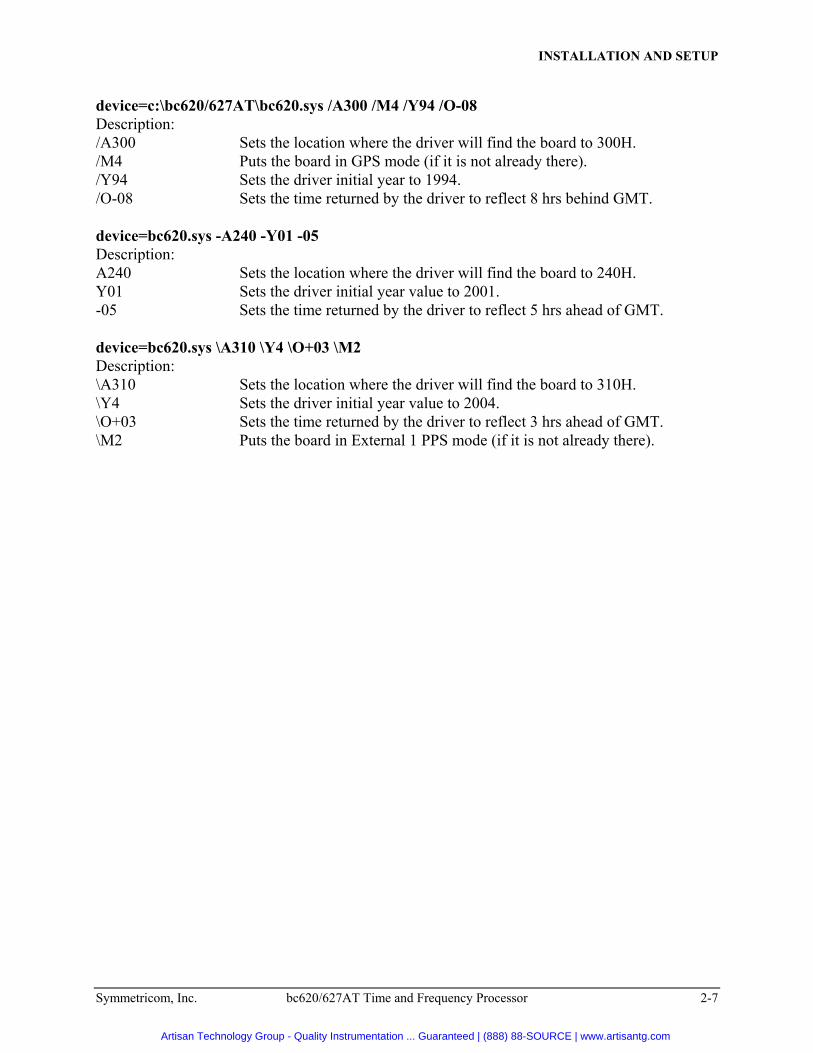
device=c:\bc620/627AT\bc620.sys /A300 /M4 /Y94 /O-08Description:/A300 Sets the location where the driver will find the board to 300H./M4 Puts the board in GPS mode (if it is not already there)./Y94 Sets the driver initial year to 1994./O-08 Sets the time returned by the driver to reflect 8 hrs behind GMT.
device=bc620.sys -A240 -Y01 -05Description:A240 Sets the location where the driver will find the board to 240H.Y01 Sets the driver initial year value to 2001.-05 Sets the time returned by the driver to reflect 5 hrs ahead of GMT.
device=bc620.sys \A310 \Y4 \O+03 \M2Description:\A310 Sets the location where the driver will find the board to 310H.\Y4 Sets the driver initial year value to 2004.\O+03 Sets the time returned by the driver to reflect 3 hrs ahead of GMT.\M2 Puts the board in External 1 PPS mode (if it is not already there).
Artisan Technology Group - Quality Instrumentation ... Guaranteed | (888) 88-SOURCE | www.artisantg.com

CHAPTER TWO
2-8 bc620/627AT Time and Frequency Processor Symmetricom, Inc.
This Page Intentionally Left Blank.
Artisan Technology Group - Quality Instrumentation ... Guaranteed | (888) 88-SOURCE | www.artisantg.com
Symmetricom Inc bc620/627AT Time and Frequency Processor 3-1
CHAPTER THREESOFTWARE INTERFACE
3.0 GENERAL
The bc620/627AT Time and Frequency Processor (TFP) occupies 16 bytes in the PC bus I/Oaddress space. Refer to Chapter Two for details on base address selection. All TFP registers areeight bits wide. This chapter describes the TFP registers and their use.
3.0.1 GLOSSARY OF KEY TERMS
EpochA reference time or event. In timing applications “epoch” often refers to a one pulse per secondevent (1pps).
FlywheelIn the time keeping vernacular, to “flywheel” means to maintain time or frequency or both afterthe input reference is removed or lost.
PeriodicA programmable frequency which is obtained by dividing the TFP reference frequency. Periodics are sometimes referred to as “heartbeats.” Periodics may optionally be synchronouswith the 1pps epoch if the period is expressible as a ratio of integers.
Major TimeUnits of time larger than or equal to seconds. A day hr:min:sec format is usually implied.
Minor TimeSubsecond time to whatever resolution is supported.
PacketA group of bytes conforming to a defined structure. Packets are usually used in bit serial or byteserial data transmission to allow framing of the transmitted data.
Artisan Technology Group - Quality Instrumentation ... Guaranteed | (888) 88-SOURCE | www.artisantg.com
CHAPTER THREE
3-2 bc620/627AT Time and Frequency Processor Symmetricom, Inc.
3.1 REGISTERS
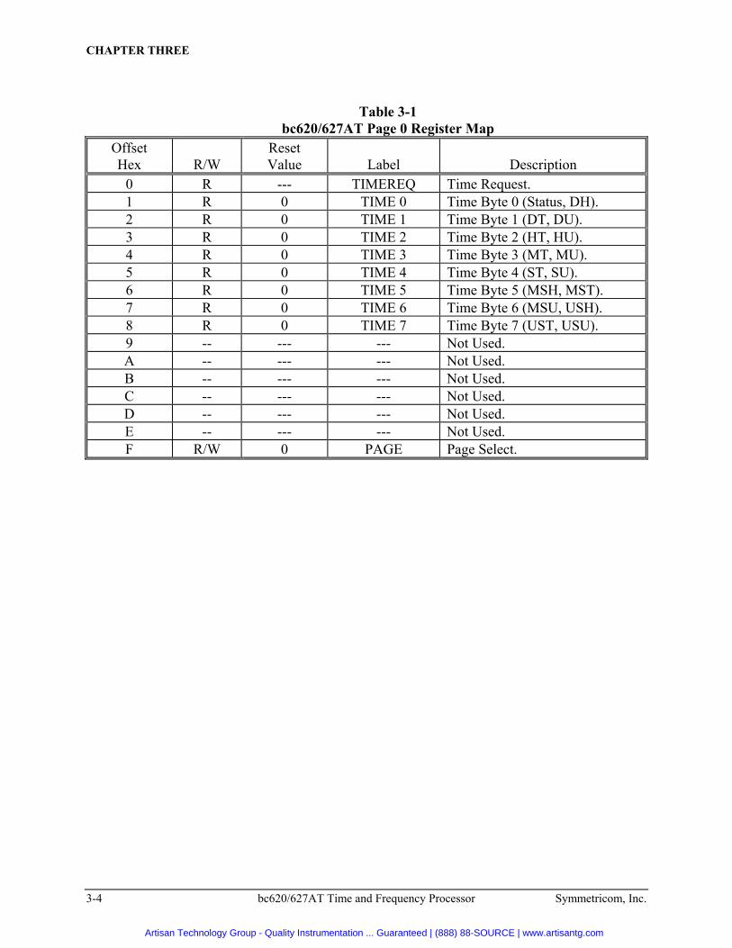
This section describes the registers used on the TFP for controlling its operation and transferringtime data. Section 3.2 details the use of these registers. There are two 16-byte pages of registerson the TFP. The page select register determines the active page and is always accessible. Thememory map for the TFP is listed in Table 3-1 and Table 3-2 (PAGE 1 registers). The firstcolumn of these tables shows the offset from the base address of each register. The secondcolumn (R/W) lists the access type of each register. These registers may be read only (R), writeonly (W), or read/write (R/W). In some cases, a read/write register is structured to supportdissimilar data in the read and write directions. The contents of each register following a power-on or software reset is shown (RESET VALUE). A reset value of “---” indicates that the registercontents are undefined. A label for each register is listed, as well as a brief description of theregister's function.
3.1.1 PAGE SELECT REGISTER (PAGE 0/1)
The page select register is used to activate one of two 16-byte banks of registers. Bit 0 of PAGEselects PAGE 0 or PAGE 1, bits 1-7 are ignored during writes and undefined during reads. PAGE is always accessible.
3.1.2 TIMEREQ AND TIME0 - TIME7 REGISTERS (PAGE 0)
Reading the TIMEREQ register causes the current time (days - microseconds) and status to beloaded into a bank of registers, freezing the time at the instant the TIMEREQ register isaccessed. Special circuitry prohibits the time from being latched while the time is changing. This circuitry is designed so that the TIME0 - TIME7 registers can be read immediately after aread of the TIMEREQ register without having to wait some predetermined amount of time(latency) for the time registers to become valid. This is referred to as zero latency time access.
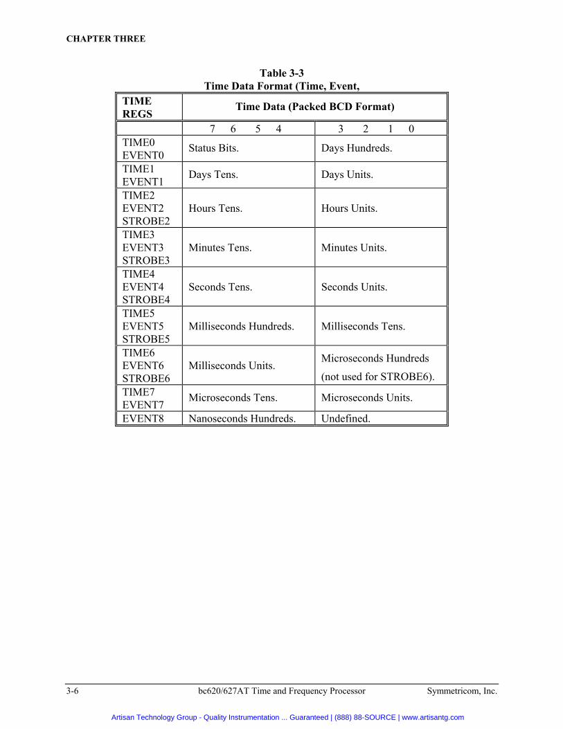
A bank of 8 byte-wide registers (TIME0 - TIME7) holds the captured time and status. The timedata is in a packed BCD format as shown in Table 3-3. The time is maintained in these registersuntil the TIMEREQ register is read again.
Artisan Technology Group - Quality Instrumentation ... Guaranteed | (888) 88-SOURCE | www.artisantg.com

SOFTWARE INTERFACE
Symmetricom, Inc. bc620/627AT Time and Frequency Processor 3-3
The status bits 4 - 6 of the TIME0 and EVENT0 register indicate the tracking status of the TFPwith respect to the selected time source.
Bit 4: 0 = Reference time source present (i.e. time code, external 1pps, etc.). 1 = Flywheeling (i.e. time source lost)
Bit 5: 0 = Synchronized to within +/- X microseconds of time source 1 = Not synchronized to within +/- X microseconds of time source
(X = 5 for Mode 0 X = 2 for all other Modes)
Bit 6: 0 = Frequency stability <= 5 parts in 10EX relative to time source 1 = Frequency stability > 5 parts in 10EX relative to time source
(X=7 for Mode 0 X=8 for all other Modes)
Bit 7: Currently unused
A second independent one-hundred nanosecond bus time request is supported with theUNLOCK and EVENT0 - EVENT8 registers. See sections 3.1.4 and 3.1.5.
Note: Register bits which are designated as “unused” are ignored during writes and undefinedduring reads. For software compatibility with future versions of the TFP, which may usesome of the “unused” bits, write zero's to these bits and ignore them during reads.
Artisan Technology Group - Quality Instrumentation ... Guaranteed | (888) 88-SOURCE | www.artisantg.com
CHAPTER THREE
3-4 bc620/627AT Time and Frequency Processor Symmetricom, Inc.
Table 3-1bc620/627AT Page 0 Register Map
OffsetHex R/W
ResetValue Label Description
0 R --- TIMEREQ Time Request.1 R 0 TIME 0 Time Byte 0 (Status, DH).2 R 0 TIME 1 Time Byte 1 (DT, DU).3 R 0 TIME 2 Time Byte 2 (HT, HU).4 R 0 TIME 3 Time Byte 3 (MT, MU).5 R 0 TIME 4 Time Byte 4 (ST, SU).6 R 0 TIME 5 Time Byte 5 (MSH, MST).7 R 0 TIME 6 Time Byte 6 (MSU, USH).8 R 0 TIME 7 Time Byte 7 (UST, USU).9 -- --- --- Not Used.A -- --- --- Not Used.B -- --- --- Not Used.C -- --- --- Not Used.D -- --- --- Not Used.E -- --- --- Not Used.F R/W 0 PAGE Page Select.
Artisan Technology Group - Quality Instrumentation ... Guaranteed | (888) 88-SOURCE | www.artisantg.com
SOFTWARE INTERFACE
Symmetricom, Inc. bc620/627AT Time and Frequency Processor 3-5
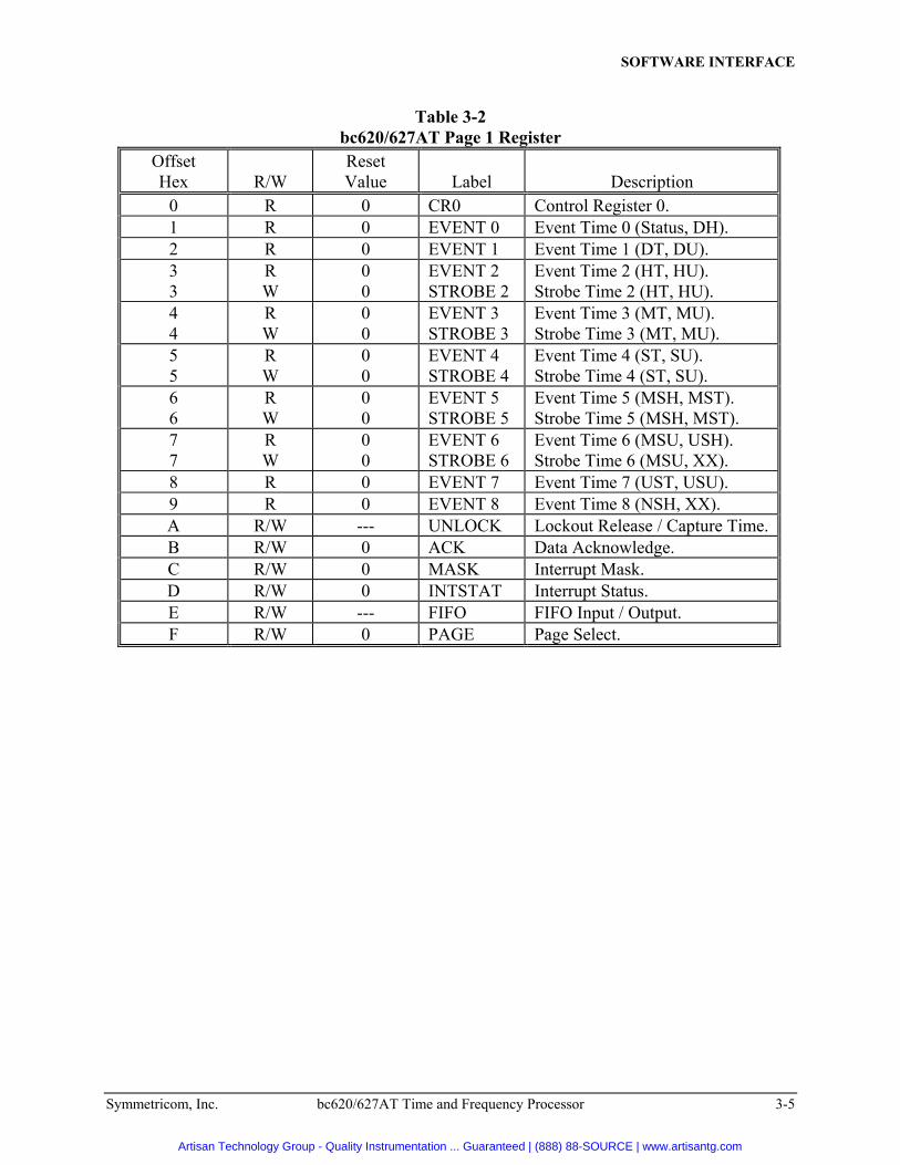
Table 3-2bc620/627AT Page 1 Register
OffsetHex R/W
ResetValue Label Description
0 R 0 CR0 Control Register 0.1 R 0 EVENT 0 Event Time 0 (Status, DH).2 R 0 EVENT 1 Event Time 1 (DT, DU).33
RW
00
EVENT 2STROBE 2
Event Time 2 (HT, HU).Strobe Time 2 (HT, HU).
44
RW
00
EVENT 3STROBE 3
Event Time 3 (MT, MU).Strobe Time 3 (MT, MU).
55
RW
00
EVENT 4STROBE 4
Event Time 4 (ST, SU).Strobe Time 4 (ST, SU).
66
RW
00
EVENT 5STROBE 5
Event Time 5 (MSH, MST).Strobe Time 5 (MSH, MST).
77
RW
00
EVENT 6STROBE 6
Event Time 6 (MSU, USH).Strobe Time 6 (MSU, XX).
8 R 0 EVENT 7 Event Time 7 (UST, USU).9 R 0 EVENT 8 Event Time 8 (NSH, XX).A R/W --- UNLOCK Lockout Release / Capture Time.B R/W 0 ACK Data Acknowledge.C R/W 0 MASK Interrupt Mask.D R/W 0 INTSTAT Interrupt Status.E R/W --- FIFO FIFO Input / Output.F R/W 0 PAGE Page Select.
Artisan Technology Group - Quality Instrumentation ... Guaranteed | (888) 88-SOURCE | www.artisantg.com
CHAPTER THREE
3-6 bc620/627AT Time and Frequency Processor Symmetricom, Inc.
Table 3-3Time Data Format (Time, Event,
TIMEREGS
Time Data (Packed BCD Format)
7 6 5 4 3 2 1 0TIME0EVENT0
Status Bits. Days Hundreds.
TIME1EVENT1
Days Tens. Days Units.
TIME2EVENT2STROBE2
Hours Tens. Hours Units.
TIME3EVENT3STROBE3
Minutes Tens. Minutes Units.
TIME4EVENT4STROBE4
Seconds Tens. Seconds Units.
TIME5EVENT5STROBE5
Milliseconds Hundreds. Milliseconds Tens.
TIME6EVENT6STROBE6
Milliseconds Units.Microseconds Hundreds
(not used for STROBE6).TIME7EVENT7
Microseconds Tens. Microseconds Units.
EVENT8 Nanoseconds Hundreds. Undefined.
Artisan Technology Group - Quality Instrumentation ... Guaranteed | (888) 88-SOURCE | www.artisantg.com
SOFTWARE INTERFACE
Symmetricom, Inc. bc620/627AT Time and Frequency Processor 3-7
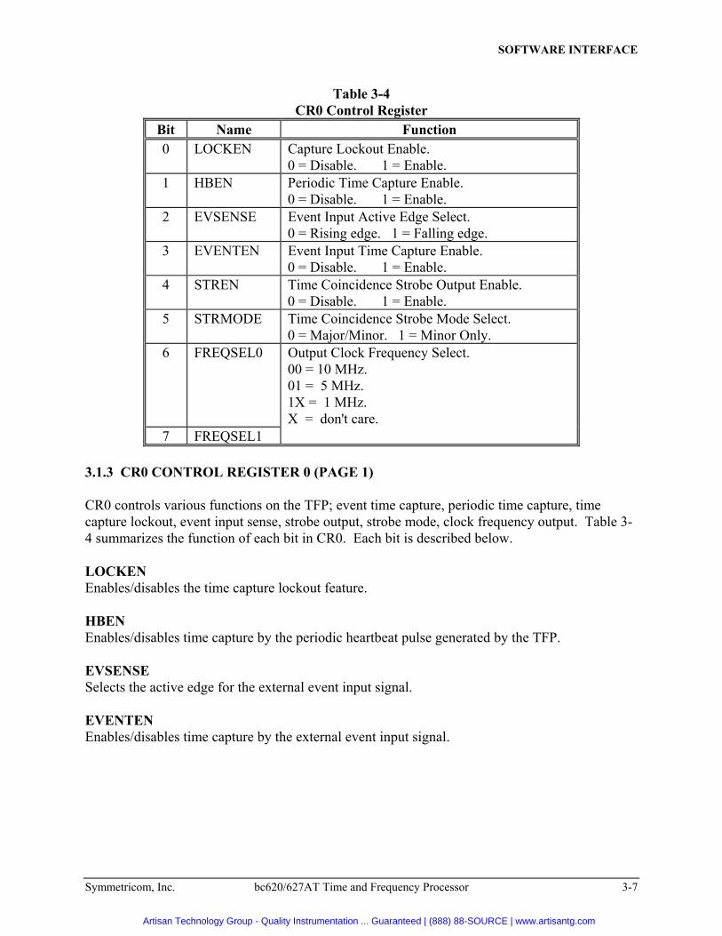
Table 3-4CR0 Control Register
Bit Name Function0 LOCKEN Capture Lockout Enable.
0 = Disable. 1 = Enable.1 HBEN Periodic Time Capture Enable.
0 = Disable. 1 = Enable.2 EVSENSE Event Input Active Edge Select.
0 = Rising edge. 1 = Falling edge.3 EVENTEN Event Input Time Capture Enable.
0 = Disable. 1 = Enable.4 STREN Time Coincidence Strobe Output Enable.
0 = Disable. 1 = Enable.5 STRMODE Time Coincidence Strobe Mode Select.
0 = Major/Minor. 1 = Minor Only.6 FREQSEL0 Output Clock Frequency Select.
00 = 10 MHz.01 = 5 MHz.1X = 1 MHz.X = don't care.
7 FREQSEL1
3.1.3 CR0 CONTROL REGISTER 0 (PAGE 1)
CR0 controls various functions on the TFP; event time capture, periodic time capture, timecapture lockout, event input sense, strobe output, strobe mode, clock frequency output. Table 3-4 summarizes the function of each bit in CR0. Each bit is described below.
LOCKENEnables/disables the time capture lockout feature.
HBENEnables/disables time capture by the periodic heartbeat pulse generated by the TFP.
EVSENSESelects the active edge for the external event input signal.
EVENTENEnables/disables time capture by the external event input signal.
Artisan Technology Group - Quality Instrumentation ... Guaranteed | (888) 88-SOURCE | www.artisantg.com

CHAPTER THREE
3-8 bc620/627AT Time and Frequency Processor Symmetricom, Inc.
STRENEnables/disables the time coincidence strobe output. When disabled, the strobe output is alwayslow.
STRMODESelects the mode of operation for the time coincidence strobe. “Major/Minor” mode generatesan output pulse when both the major time (hours - seconds) and the minor time (milliseconds)match the programmed strobe time (STROBE2 - STROBE6). “Minor Only” mode generates anoutput pulse when the minor time matches the programmed strobe time (i.e. once per second).
FREQSEL0,1Selects one of three clock output frequencies. The output frequency is either 1, 5, or 10 MHz.
3.1.4 EVENT0 - EVENT8 TIME CAPTURE REGISTERS (PAGE 1)
The EVENT0 - EVENT8 registers hold time which has been captured in response to the activeedge of the external event input the programmable periodic output, or a bus time requestaccomplished by writing to the UNLOCK register. Time is captured only when the capturesources (i.e. external event or periodic) are enabled with Bits 1 and 3 of CR0. This set of timecapture registers is completely separate from the TIME0 - TIME7 registers on page 0. Time iscaptured to a resolution of 100 nanoseconds. The time capture lockout feature prevents theEVENT0 - EVENT8 registers from being overwritten with a new time before they can be read(See Section 3.2.3.3). Table 3-3 shows the time data format for these registers.
3.1.5 UNLOCK REGISTER (PAGE 1)
To release the time capture lockout mechanism, the UNLOCK register is read. The data readfrom UNLOCK is undefined.
A write to the UNLOCK register latches time in the EVENT0 - EVENT8 registers. The datawritten to the UNLOCK register is insignificant. This feature allows two independent times tobe captured via the PCbus by the host CPU
3.1.6 ACK REGISTER (PAGE 1)
The ACK data acknowledge register provides a means for acknowledging a data transfer to/fromthe TFP via the FIFO interface, provides a mechanism for clearing the output FIFO and providesa 1pps flag bit. Table 3-5 summarizes the function of each bit in the ACK register.
FIFO RX (Bit 0)The 620/627AT acknowledges receipt of a valid input FIFO data packet by setting this bit. Theuser is responsible for clearing the bit before instructing the TFP to take action on the FIFO data. (Refer to bit 7).
Artisan Technology Group - Quality Instrumentation ... Guaranteed | (888) 88-SOURCE | www.artisantg.com

SOFTWARE INTERFACE
Symmetricom, Inc. bc620/627AT Time and Frequency Processor 3-9
1 PPS (Bit 1)This bit is set by the TFP once each second with the rising edge of the on-time 1pps output pulse. The user is responsible for clearing the bit.
FIFO RDY (Bit 2)The 620AT sets this bit when an output FIFO data packet is ready to be read by the host.
EF/CLR FIFO (Bit 4)A read of this bit returns the output FIFO empty flag status. When reading data from the FIFOthis bit is monitored to insure all the FIFO data is read. The bit is clear (zero) when the FIFO isempty.
Writing a one to this register bit clears the output FIFO of all data and sets the empty flag tozero.
FIFO PACKET RDY (Bit 7)Writing a one to this bit causes the TFP to take action on the input FIFO packet data.
Note: Acknowledge register bits 0, 1, 2 are cleared by writing a one to that bit location. Forexample, writing the value 0x01 to ACK will clear bit 0 and leave bit 1 unaltered. Writing the value 0x03 to ACK will clear both bit 0 and bit 1.
Table 3-5ACK Acknowledge Register
bit# CONTROL FUNCTION (SET = “1” = high voltage CLEAR = “0” = lowvoltage).
0 TFPHOST
SETS bit to acknowledge the receipt of a valid input packet from host.CLEARS bit by writing to this register with bit 0 SET.
1 Reserved.2 TFP
HOSTSETS bit when output FIFO contains a data packet.CLEARS bit by writing to this register with bit 2 SET.This bit can generate an interrupt. (See Section 3.1.7.)
3 Reserved.4 TFP
HOSTSETS bit if output FIFO contains data. CLEARS bit if output FIFOempty. CLEARS output FIFO by writing to this register with bit 4SET.
5 Reserved.6 Reserved.7 HOST Must write to this register with bit 7 SET to cause TFP to take
action on the data packet previously written to the input FIFO.
Artisan Technology Group - Quality Instrumentation ... Guaranteed | (888) 88-SOURCE | www.artisantg.com
CHAPTER THREE
3-10 bc620/627AT Time and Frequency Processor Symmetricom, Inc.
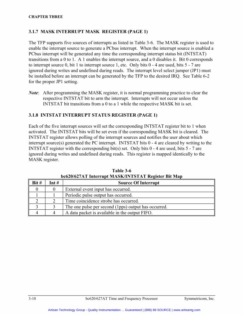
3.1.7 MASK INTERRUPT MASK REGISTER (PAGE 1)
The TFP supports five sources of interrupts as listed in Table 3-6. The MASK register is used toenable the interrupt source to generate a PCbus interrupt. When the interrupt source is enabled aPCbus interrupt will be generated any time the corresponding interrupt status bit (INTSTAT)transitions from a 0 to 1. A 1 enables the interrupt source, and a 0 disables it. Bit 0 correspondsto interrupt source 0, bit 1 to interrupt source 1, etc. Only bits 0 - 4 are used, bits 5 - 7 areignored during writes and undefined during reads. The interrupt level select jumper (JP1) mustbe installed before an interrupt can be generated by the TFP to the desired IRQ. See Table 6-2for the proper JP1 setting.
Note: After programming the MASK register, it is normal programming practice to clear therespective INTSTAT bit to arm the interrupt. Interrupts will not occur unless theINTSTAT bit transitions from a 0 to a 1 while the respective MASK bit is set.
3.1.8 INTSTAT INTERRUPT STATUS REGISTER (PAGE 1)
Each of the five interrupt sources will set the corresponding INTSTAT register bit to 1 whenactivated. The INTSTAT bits will be set even if the corresponding MASK bit is cleared. TheINTSTAT register allows polling of the interrupt sources and notifies the user about whichinterrupt source(s) generated the PC interrupt. INTSTAT bits 0 - 4 are cleared by writing to theINTSTAT register with the corresponding bit(s) set. Only bits 0 - 4 are used, bits 5 - 7 areignored during writes and undefined during reads. This register is mapped identically to theMASK register.
Table 3-6bc620/627AT Interrupt MASK/INTSTAT Register Bit Map
Bit # Int # Source Of Interrupt0 0 External event input has occurred.1 1 Periodic pulse output has occurred.2 2 Time coincidence strobe has occurred.3 3 The one pulse per second (1pps) output has occurred.4 4 A data packet is available in the output FIFO.
Artisan Technology Group - Quality Instrumentation ... Guaranteed | (888) 88-SOURCE | www.artisantg.com
SOFTWARE INTERFACE
Symmetricom, Inc. bc620/627AT Time and Frequency Processor 3-11
3.1.9 FIFO REGISTER (PAGE 1)
The TFP uses two FIFO (First-In First-Out) buffers; one to hold data packets written to the TFPfor setting time, setting the programmable periodic rate, etc. (Input FIFO); and one to hold datapackets from the TFP (Output FIFO). Each FIFO holds up to 512 bytes of data.
3.1.10 STROBE2 - STROBE6 TIME COINCIDENT STROBE REGISTERS (PAGE 1)
STROBE2 - STROBE6 registers hold the time coincidence strobe time from hours throughmilliseconds. Table 3-3 shows the time data format for these registers.
3.2 FUNCTIONAL DESCRIPTION
This section provides a description of how to use these registers to achieve the desired function.
3.2.1 CHANGING THE ACTIVE PAGE
To access the page 0 registers write 0x00 to PAGE. To access the page one registers write 0x01to PAGE. The respective PAGE registers will be active until the PAGE register is changed.
3.2.2 READING TIME ON DEMAND
A read of the TIMEREQ register will latch the current time (days through microseconds), andthis time will remain in the TIME0 - TIME7 registers until a subsequent read of TIMEREQ. TheTIME0 -TIME7 registers can be read immediately after reading TIMEREQ.
A second bus time request is supported with the EVENT time capture registers. A write to theUNLOCK register latches time (days through 0.1 microseconds) in the EVENT0 - EVENT8 registers. The EVENT0 - EVENT8 registers can be read immediately after writing the UNLOCKregister.
3.2.3 EVENT TIME CAPTURE
The EVENT0 - EVENT8 registers are used to hold time which has been captured in response tothe active edge of the external event input, the programmable periodic output, or a write to theUNLOCK register. As with the TIME0 - TIME7 registers, the EVENT0 - EVENT8 registerscan be read immediately after the event has occurred.
Artisan Technology Group - Quality Instrumentation ... Guaranteed | (888) 88-SOURCE | www.artisantg.com

CHAPTER THREE
3-12 bc620/627AT Time and Frequency Processor Symmetricom, Inc.
3.2.3.1 EXTERNAL EVENT INPUT
The external event input provides a means of capturing time based on an event that occursexternally to the TFP. Use the EVENTEN bit (CR0 bit 3) to enable the external event timecapture. Use the EVSENSE bit (CR0 bit 2) to select the active edge. When the active edge ofthe external event input occurs, INTSTAT bit 0 will be set, and if MASK bit 0 is set a PC ATbus interrupt will be generated.
3.2.3.2 PROGRAMMABLE PERIODIC OUTPUT
The programmable periodic output will capture time in the EVENT0 - EVENT8 registers if theHBEN bit (CR0 bit 0) is set to 1. When the rising edge of the periodic output occurs, INTSTATbit 1 will be set, and if MASK bit 1 is set a PC AT bus interrupt will be generated. The periodicoutput rate is programmable over the range from 2.5 MHz to 2.3 MHz.
3.2.3.3 TIME CAPTURE LOCKOUT
Time capture lockout is used with the event capture registers to prevent them from beingoverwritten before they can be read. The lockout (if enabled) will allow a capture signal(external event or periodic) to capture time once, then subsequent capture signals will be blockeduntil the lockout is released. The lockout is released by reading the UNLOCK register. Thetime capture lockout feature is enabled with LOCKEN (CR0 bit 0).
A write instruction to the UNLOCK register will latch time in the EVENT0 - EVENT8 registers.
3.2.4 TIME COINCIDENCE STROBE OUTPUT
The TFP provides a time coincidence strobe output which generates a one millisecond widepulse (rising edge on time) at the time set in the STROBE2 - STROBE6 registers. Use STREN(CR0 bit 4) to enable/disable the strobe output pulse. When changing the STROBE2 -STROBE6 registers, the strobe output should be disabled to prevent false strobe outputs. Thestrobe can be operated in one of two modes: “major/minor” mode or “minor only” mode. Inmajor/minor mode, the strobe output pulse occurs when the time matches both the programmedmajor time (hours - seconds) and the programmed minor time (milliseconds). In minor onlymode, the strobe output pulse occurs once per second when the time matches the programmedminor time. The rising edge of the strobe will set INTSTAT bit 2, and if MASK bit 2 is set a PC,AT bus interrupt will be generated.
Artisan Technology Group - Quality Instrumentation ... Guaranteed | (888) 88-SOURCE | www.artisantg.com
SOFTWARE INTERFACE
Symmetricom, Inc. bc620/627AT Time and Frequency Processor 3-13
3.2.5 FIFO INTERFACE - PROGRAMMING THE BC620/627AT
Reads cycles take data from the output FIFO. Writes cycles place data into the input FIFO. Both the input FIFO and the output FIFO may be accessed at offset 0x0E of register PAGE 1. Each FIFO has a depth of 512 bytes.
Data must be written to and read from the FIFO in the following data packet format:
byte 1 0x01 header byte (ASCII SOH).byte 2 “A” through “Z” idbyte.byte 3 Data always ASCII (i.e. 0 = 0x30).byte 4 Data. . . . . The number of data bytes varies.byte N Data.byte N+1 0x17 tail byte (ASCII ETB).
See Chapter Four for a description of the available FIFO data packets and programmingprotocol.
3.3 PC AT INTERRUPTS
The TFP supports the five interrupt sources listed in Table 3-6. Interrupts are maskable with theMASK register. When multiple interrupt sources are enabled in the MASK register, the interruptservice routine can read the INTSTAT register to determine which interrupt source(s) caused theinterrupt. Interrupt source activity can be polled by disabling interrupts (MASK register = 0)and then reading the INTSTAT register to determine when an interrupt signal is activated. Theinterrupt jumper JP1 on the TFP allows interrupt level selection. The TFP supports interruptlevels IRQ3-7, IRQ9-12, and IRQ14-15.
Artisan Technology Group - Quality Instrumentation ... Guaranteed | (888) 88-SOURCE | www.artisantg.com

CHAPTER THREE
3-14 bc620/627AT Time and Frequency Processor Symmetricom, Inc.
This Page Intentionally Left Blank.
Artisan Technology Group - Quality Instrumentation ... Guaranteed | (888) 88-SOURCE | www.artisantg.com
Symmetricom, Inc. bc620/627AT Time and Frequency Processor 4-1
CHAPTER FOURFIFO DATA PACKETS
4.0 GENERAL
Communication with the bc620/627AT Time and Frequency Processor (TFP) is performed usingbyte serial data packet protocol. The packet bytes are read from and written to the TFP usingeight bit data transfers at offset 0x0E of PAGE1. Following is a description of the availableTFP FIFO data packets and the programming protocol.
4.1 WRITING DATA PACKETS
The following steps should be followed when loading data packets to the TFP. Failure toperform one or more of these steps correctly is a common reason for customer support calls.
• Write the packet to the input FIFO. • Clear bit zero of the ACK register by writing 0x01 to the ACK register. • Inform the TFP that an input packet is available by writing 0x80 to the ACK register. • The TFP will set bit zero of the ACK register when the packet is processed. When the host sets bit 7 of the ACK register and an interrupt is generated to the TFP CPU, theTFP service routine performs minimalist packet integrity checking. The TFP checks that thefirst packet byte is 0x01 (ASCII SOH). If the SOH is found, the TFP loads FIFO data into aninput buffer until a byte value of 0x17 (ASCII ETB) is found. The packet is then processed inaccordance with the idbyte value. When processing is complete the TFP sets bit 1 of the ACKregister, clears the input FIFO, and resumes its previous task. If an SOH is not the first packetbyte or if more than 40 bytes are read before encountering an ETB or if the idbyte value isinvalid, then TFP clears the FIFO, sets bits 1 of the ACK register, and resumes its previous task. A demonstration program written in the “C” language is provided with the disk accompanyingthe TFP. This program demonstrates the use of the primary data packets described below. 4.1.1 PACKET “A” - SELECT OPERATIONAL MODE This packet contains a single data byte defining the operational mode of the TFP. Fiveoperational modes are supported, modes 0, 1, 2, 3, and 4 corresponding to ASCII data bytes “0,”“1,” ... “4.”
Artisan Technology Group - Quality Instrumentation ... Guaranteed | (888) 88-SOURCE | www.artisantg.com

CHAPTER FOUR
4-2 bc620/627AT Time and Frequency Processor Symmetricom, Inc.
MODE 0 TIME CODE DECODING MODE The TFP uses an input time code as the timing reference. The following codes are supported(see packet “H”): IRIG A, and B; 2137, XR3; and NASA36. Both modulated carrier and DClevel shift formats are supported (DC level shift is not supported for 2137 or XR3 codes). TheTFP locks its crystal oscillator to the input code rate. The oscillator has a control range of +/- 30PPM for the standard VCXO version, and ± 2 PPM for the optional oven (OCXO) version. Ifthe input code is outside these limits the TFP will exhibit periodic slips (i.e., if the TFP referencedeviates from the input source by more than ± 1 millisecond a forced jamsync is performed). Ifthe input code is lost or removed the TFP will continue to “flywheel” at the last known code rate. Typical accuracy is less than five parts in 10E7 (two milliseconds of drift per hour). MODE 1 FREE RUNNING MODE This mode is virtually the same as mode 2. Without a 1pps input the TFP runs at the last knownoscillator frequency. Major time can be set with the “B” packet. The TFP time base can beadjusted with packet “D.” MODE 2 EXTERNAL 1PPS MODE The TFP synchronizes to the external 1pps input signal. Major time can be loaded with the “B”packet. The acquisition range is the same as described in mode 0. MODE 2 is used when a primary time standard such as a GPS receiver is available. In this casethe 1pps output of the standard is input to the TFP. MODE 3 REAL TIME CLOCK MODE The TFP synchronizes to a 1pps signal from the on-board real time clock (RTC) IC, and themajor time is also derived from the clock IC. The RTC is battery backed. This mode is notrecommended when using the oven oscillator because the accuracy of the RTC is not highenough to ensure that the oven will be able to track it with slippage. See Mode 0 description. MODE 4 GPS MODE (bc627AT GPS Satellite Receiver) This optional mode is discussed in the bc627AT GPS Satellite Receiver Addendum User’sGuide. The bc620.c file has an example function, mode(), which sets the TFP operational mode asdescribed above.
Artisan Technology Group - Quality Instrumentation ... Guaranteed | (888) 88-SOURCE | www.artisantg.com

FIFO DATA PACKETS
Symmetricom, Inc. bc620/627AT Time and Frequency Processor 4-3
4.1.2 PACKET “B” - SET MAJOR TIME TFP Modes 1 and 2 require the major time to be input using this data packet. Modes 0, 3 and 4acquire major time from their respective time sources. Set time in Mode 3 with Packet “L.” Packet “B” can be used to load time in any mode when the TFP is flywheeling. The data field ofthis packet consists of nine ASCII time digits in the order of seconds through days as follows:
byte 1 SOH. byte 2 “B.” byte 3 Seconds Units. byte 4 Seconds Tens. byte 5 Minutes Units. byte 6 Minutes Tens. byte 7 Hours Units. byte 8 Hours Tens. byte 9 Days Units (JAN 1 = DAY 001). byte 10 Days Tens. byte 11 Days Hundreds. byte 12 ETB.
The following paragraphs are about timing. This information should be well understood to avoid problems loading the major time. The TFP firmware partitions each one second epoch into 30 periods plus a fractional period. Each period is 65536 counts of a 2 MHz clock. If the 2 MHz clock was perfect and the onesecond epoch was perfect then the number of counts in the one second epoch would be exactlytwo million. There would be thirty periods plus a remainder of 33920 counts. For now it is important to know that the bc620/627AT increments, and then transfers major time,from a software buffer to a set of hardware latches on the 29th period of the internal counter. The time loaded into the latches will be the major time used for the next one second epoch (i.e.the next 1pps pulse rising edge transfers the time loaded at the 29th period to a second set oflatches that are used for the major time reference). This double buffering approach ensures thatthe major and minor times are completely coherent, and that no ambiguities occur during the1pps transition. What does all this mean? When loading the major time observe the followingrules: • If time is loaded before 29/30 into the second then the loaded time should reference the
current epoch. (Recall the bc620 increments major time before downloading to the hardwarelatches.)
• If time is loaded after 29/30 into the second then the loaded time should reference the
following epoch.
Artisan Technology Group - Quality Instrumentation ... Guaranteed | (888) 88-SOURCE | www.artisantg.com

CHAPTER FOUR
4-4 bc620/627AT Time and Frequency Processor Symmetricom, Inc.
• Avoid loading major time near 29/30 into the second for obvious reasons. • The loaded time will not be output by the bc620 at the next 1pps on-time mark. So don't
expect your download to be used before the appropriate 1pps occurs.
The bc620.c file has an example function, load_clock(), which sets the time as described above.
4.1.3 PACKET “C” - COMMAND INPUT
This packet allows the user to exercise some direct control of the bc620 firmware. Fivecommands are supported at this time. These are:
“1” WARMSTART - Perform a reset without variable initialization. (Defaults not loaded.)
“2” RESET - Same as power on reset.
“3” JAMSYNCH - Forces minor time to jam to zero on the next 1pps pulse.
“4” !JAMSYNCH - Disable any pending jamsynch.
“5” Sync RTC - Synchronizes the battery back RTC IC time to current TFP time.
Commands three and four are provided for advanced users who may need to exercise controlover the normal flow of the bc620 firmware. Issuing a jam sync can be useful when using anexternal fixed oscillator that can not be disciplined. Command four has no known usefulpurpose. It was initially implemented during the TFP checkout phase and has not been removed.
The bc620.c file has an example function, command(), which downloads a command asdescribed above.
4.1.4 PACKET “D” - LOAD THE D/A CONVERTER
The TFP disciplines a reference oscillator using a DC control voltage which is the bufferedoutput of a 16 bit D/A converter. This voltage is routed to an on board 10 MHz VCXO and topin#1 on rear panel connector J1 to discipline an external oscillator. The control equations arecompatible with virtually any oscillator which has a positive voltage versus frequency controlcharacteristic (increasing voltage = increasing frequency).
Artisan Technology Group - Quality Instrumentation ... Guaranteed | (888) 88-SOURCE | www.artisantg.com

FIFO DATA PACKETS
Symmetricom, Inc. bc620/627AT Time and Frequency Processor 4-5
The TFP divides the reference frequency input (whether input from an external 10 MHz source or the on-board 10 MHz VCXO) to produce a 1pps pulse. This pulse is compared to thereference 1pps epoch which is derived from the selected time reference (i.e., time code, external1pps etc.). The D/A voltage is adjusted to steer the 1pps derived from the voltage controlledoscillator into phase coherence with the reference 1pps.
Some users may wish to control the D/A converter directly. Packet “D” is provided for thispurpose. The format is as follows:
byte 1 SOH.byte 2 “D.”byte 3 ASCII “0” - “F” (bits 12 through 15)..byte 4 ASCII “0” - “F” (bits 8 through 11).byte 5 ASCII “0” - “F” (bits 4 through 7).byte 6 ASCII “0” - “F” (bits 0 through 3).byte 7 ETB.
The bc620 firmware routines which normally load the D/A (i.e. disciplining) must be disabledusing the path packet “P” to prevent the bc620 from overwriting the data input with this packet(“D”).
The bc620.c file has an example function, preset_DA( ), which presets the D/A as describedabove.
4.1.5 PACKET “F” - HEARTBEAT (PERIODICS) CONTROL
The programmable frequency output is a very powerful bc620/627AT feature. Feedback fromthe users of other board level products motivated the inclusion of a very comprehensive periodicprogramming capability. Rates from 2.5 MHz to 2.3 MHz are easily achieved.
The heartbeat engine of the bc620/627AT consists of two sections of an INTEL 82C54programmable interval timer connected in a serial configuration and driven by the TFP 10 MHzreference. Glue logic in one of the logic cell arrays supports both synchronous (with the 1ppsepoch) and asynchronous operation. It is helpful (although not essential) to read the INTEL datasheet on the 82C54. Packet “F” allows the user complete access to the serial counters usingstandard INTEL loading protocols.
Artisan Technology Group - Quality Instrumentation ... Guaranteed | (888) 88-SOURCE | www.artisantg.com
CHAPTER FOUR
4-6 bc620/627AT Time and Frequency Processor Symmetricom, Inc.
Two counter modes are supported; 1pps synchronous and asynchronous. It is the responsibilityof the user to select the appropriate mode. No error checking is performed by the bc620/627ATfirmware. The synchronous mode should only be selected if the number of output counts persecond is an integer. If the number of counts per second is not an integer then the asynchronousmode should be used. The number of counts per second is always of the following form:
N = (10,000,000) / (n1 * n2)
where: N = counts per secondn1 = Counter #1 dividen2 = Counter #2 divide
The range of values for Counter #1 and #2 is mode dependent as follows.
Asynchronous Mode: 2 to 65535Synchronous Mode: 3 to 65535
* * * WARNING * * *
Periodic heartbeat pulse/interrupt generation can not be guaranteed in synchronous mode whencounter divide values of two are used.
The two modes of operation are accessed using standard INTEL mode identifiers. Forsynchronous operation the mode byte must be an ASCII “5.” For asynchronous operation themode byte must be an ASCII “2.” The packet format is as follows:
byte 1 SOH.byte 2 “F.”byte 3 ASCII “2” (asynch) or ASCII “5” (synch).byte 4 ASCII “0” - ”F” (n1 bits 12 through 15).byte 5 ASCII “0” - ”F” (n1 bits 8 through 11).byte 6 ASCII “0” - ”F” (n1 bits 4 through 7).byte 7 ASCII “0” - ”F” (n1 bits 0 through 3).byte 8 ASCII “0” - ”F” (n2 bits 12 through 15).byte 9 ASCII “0” - ”F” (n2 bits 8 through 11).byte 10 ASCII “0” - ”F” (n2 bits 4 through 7).byte 11 ASCII “0” - ”F” (n2 bits 0 through 3).byte 12 ETB.
Artisan Technology Group - Quality Instrumentation ... Guaranteed | (888) 88-SOURCE | www.artisantg.com

FIFO DATA PACKETS
Symmetricom, Inc. bc620/627AT Time and Frequency Processor 4-7
* * * IMPORTANT * * *
When Mode 5 is used, the value of n1 and n2 produced by the 82C54 hardware is n1+1 andn2+1. This is a result of the way INTEL designed the 82C54, and is unrelated to our design.
Example: It is desired to implement 10000 counts per second synchronous with the 1pps.
mode = “5” (synchronous)n1+1 = 10n2+1 = 100 (10,000,000) / (10 * 100) = 10000
Other values of (n1+1) and (n2+1) could have been used.For example, (n1+1) = 25 and (n2+1) = 40.
byte 1 SOH.byte 2 “F.”byte 3 “5” (mode).byte 4 “0.”byte 5 “0.”byte 6 “0.”byte 7 “9” (n1 = 9).byte 8 “0.”byte 9 “0.”byte 10 “6.”byte 11 “3” (n2 = 99 = 0x63).byte 12 ETB.
The bc620.c file has an example function, load_82C54( ), illustrating the use of this packet.
4.1.6 PACKET “G” - PROPAGATION DELAY OFFSET CONTROL
It is frequently desirable to be able to program an offset into the basic timekeeping functions,relative to the reference input. For example, if the reference input is IRIG B test range time,there may be a significant cable propagation delay between the IRIG B source and the bc620.This delay may be removed by simply advancing the bc620/627AT from the reference by theknown delay. The offset is programmable in steps of one-hundred nanoseconds (7 digits plus thesign byte spans a one second range).
Artisan Technology Group - Quality Instrumentation ... Guaranteed | (888) 88-SOURCE | www.artisantg.com
CHAPTER FOUR
4-8 bc620/627AT Time and Frequency Processor Symmetricom, Inc.
The packet format is as follows:
byte 1 SOH.byte 2 “G.”byte 3 ASCII “±” (advance/retard).byte 4 ASCII “0” - ”9” (most significant digit). . . . .byte 10 ASCII “0” - ”9” (least significant digit).byte 11 ETB.
* * * WARNING * * *
If offsets larger than +/- 990 microseconds are used, then the TFP jamsynch feature must beturned off using packet “P.” The reason for this requirement is that under normal operation if adifference between the reference time and the TFP time is detected to be greater than +/- 1millisecond the TFP time base is “jammed” to the reference time so that a lengthy steeringprocess is avoided.
4.1.7 PACKET “H” - SET TIME CODE FORMAT FOR MODE 0
Packet “H” allows the host to select the format and modulation type. The packet format is asfollows. The time code format and modulation values are maintained in battery backed RAM.
byte 1 SOH.byte 2 “H.”byte 3 Format.byte 4 Modulation.byte 5 ETB.
Format Choices“A” IRIG A.“B” IRIG B.“C” 2137 (XR3 with 100 Hz symbol rate).“N” NASA36.“X” XR3 (25 Hz symbol rate).
Artisan Technology Group - Quality Instrumentation ... Guaranteed | (888) 88-SOURCE | www.artisantg.com
FIFO DATA PACKETS
Symmetricom, Inc. bc620/627AT Time and Frequency Processor 4-9
Modulation Choices“M” Amplitude modulated sinewave.“D” Pulse code modulation (DC level shift).
DC level shift not is supported for 2137 and XR3 codes.
4.1.8 PACKET “I” - CLOCK SOURCE SELECT
Packet “I” is used to select the clock source for the TFP. The TFP uses a frequency of 10MHzfor all timing functions. The 10MHz be may derived from the TFP VCXO or it may be suppliedfrom an external oscillator via J1 pin#1. The packet format is as follows:
byte 1 SOH.byte 2 “I.”byte 3 “E” or “I” External or Internal.byte 4 ETB.
On power on the TFP always defaults to the internal oscillator selection.
4.1.9 PACKET “J” - SEND DATA TO THE GPS RECEIVER (bc627AT only)
The format and content variations are discussed in a separate User's Guide.
4.1.10 PACKET “K” - SELECT GENERATOR CODE
The time code generated by the TFP is selected by packet “K.” Only two options are availableas described below. The generator code type is maintained in battery backed RAM.
byte 1 SOH.byte 2 “K.”byte 3 Code.byte 4 ETB.
Code Options“B” Generate IRIG B amplitude modulated and DC level shift.“H” Generate IRIG H DC level shift only.
Artisan Technology Group - Quality Instrumentation ... Guaranteed | (888) 88-SOURCE | www.artisantg.com
CHAPTER FOUR
4-10 bc620/627AT Time and Frequency Processor Symmetricom, Inc.
4.1.11 PACKET “L”' - SET REAL TIME CLOCK
This packet loads the battery backed real time clock IC which is used as the source of major timeand 1pps epoch when mode 3 is selected. The format follows:
byte 1 SOH.byte 2 “L.”byte 3 Years Tens.byte 4 Years Units.byte 5 Months Tens.byte 6 Months Units (January = month 1).byte 7 Day of Month Tens.byte 8 Day of Month Units.byte 9 Hours Tens.byte 10 Hours Units.byte 11 Minutes Tens.byte 12 Minutes Units.byte 13 Seconds Tens.byte 14 Seconds Units.byte 15 ETB.
As usual all data is in the ASCII format. The TFP need not be in Mode 3 when packet “L”' isdownloaded.
4.1.12 PACKET “M” - LOCAL TIME OFFSET SELECT ( bc627AT GPS Mode 4 Only)
This packet allows time to be maintained with an hour offset. This situation usually arises whenthe source of time is in a UTC (Universal Time Coordinated) format and the local time isrequired from the TFP. The offset only applies to the hours digits. The format is as follows:
byte 1 SOH.byte 2 “M.”byte 3 Sign “+” or “-”.byte 4 Hours Tens.byte 5 Hours Units.byte 6 ETB.
A positive sign is from the prime meridian heading East, and a negative sign is used from theprime meridian heading West. For example, Eastern Standard Time would be -05 relative toUTC.
Artisan Technology Group - Quality Instrumentation ... Guaranteed | (888) 88-SOURCE | www.artisantg.com
FIFO DATA PACKETS
Symmetricom, Inc. bc620/627AT Time and Frequency Processor 4-11
4.1.13 PACKET “O” - REQUEST DATA FROM THE bc620/627AT
This packet is used to request data from the TFP which is not available via the register interfaces.It was added primarily to allow the user to verify the integrity of the programmed setup data. This packet has been created with a very extensible format, and additional data will be madeavailable as customer needs and suggestions are addressed.
The TFP signals a packet ready condition by setting bit2 in the ACK register. It is theresponsibility of the host to clear this bit by writing to the ACK register with bit2 set.
Note: The user is advised against repetitively issuing Packet “O” to the TFP. Processingoverhead is introduced to the TFP on-board CPU which could momentarily disrupt timekeeping.
The packet format follows:
REQUEST FORMATbyte 1 SOH.byte 2 “O” (Upper case letter).byte 3 “0” or “1” or “2.”byte 4 ETB.
RESPONSE FORMAT “0” REQUEST RTC TIME (see Packet “L”')byte 1 SOH.byte 2 “o” (Lower case letter).byte 3 “0” (ASCII zero).byte 4 Years Tens.byte 5 Years Units.byte 6 Months Tens.byte 7 Months Units.byte 8 Day of Month Tens.byte 9 Day of Month Units.byte 10 Hours Tens.byte 11 Hours Units.byte 12 Minutes Tens.byte 13 Minutes Units.byte 14 Seconds Tens.byte 15 Seconds Units.byte 16 ETB.
Artisan Technology Group - Quality Instrumentation ... Guaranteed | (888) 88-SOURCE | www.artisantg.com

CHAPTER FOUR
4-12 bc620/627AT Time and Frequency Processor Symmetricom, Inc.
RESPONSE FORMAT “1” REQUEST CURRENT D TO A VALUE(See Packet “D”)byte 1 SOH.byte 2 “o” (Lower case letter).byte 3 “1.”byte 4 “0” - “F” bits 12-15.byte 5 “0” - “F” bits 08-11.byte 6 “0” - “F” bits 04-07.byte 7 “0” - “F” bits 00-03.byte 8 ETB.
RESPONSE FORMAT “2” REQUEST LEAP SECONDS(currently GPS specific)byte 1 SOH.byte 2 “o” (Lower case letter).byte 3 “2.”byte 4 Leap Second Tens.byte 5 Leap Second Units.byte 6 ETB
Artisan Technology Group - Quality Instrumentation ... Guaranteed | (888) 88-SOURCE | www.artisantg.com
FIFO DATA PACKETS
Symmetricom, Inc. bc620/627AT Time and Frequency Processor 4-13
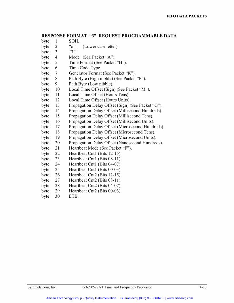
RESPONSE FORMAT “3” REQUEST PROGRAMMABLE DATAbyte 1 SOH.byte 2 “o” (Lower case letter).byte 3 “3.”byte 4 Mode (See Packet “A”).byte 5 Time Format (See Packet “H”).byte 6 Time Code Type.byte 7 Generator Format (See Packet “K”).byte 8 Path Byte (High nibble) (See Packet “P”).byte 9 Path Byte (Low nibble).byte 10 Local Time Offset (Sign) (See Packet “M”).byte 11 Local Time Offset (Hours Tens).byte 12 Local Time Offset (Hours Units).byte 13 Propagation Delay Offset (Sign) (See Packet “G”).byte 14 Propagation Delay Offset (Millisecond Hundreds).byte 15 Propagation Delay Offset (Millisecond Tens).byte 16 Propagation Delay Offset (Millisecond Units).byte 17 Propagation Delay Offset (Microsecond Hundreds).byte 18 Propagation Delay Offset (Microsecond Tens).byte 19 Propagation Delay Offset (Microsecond Units).byte 20 Propagation Delay Offset (Nanosecond Hundreds).byte 21 Heartbeat Mode (See Packet “F”).byte 22 Heartbeat Cnt1 (Bits 12-15).byte 23 Heartbeat Cnt1 (Bits 08-11).byte 24 Heartbeat Cnt1 (Bits 04-07).byte 25 Heartbeat Cnt1 (Bits 00-03).byte 26 Heartbeat Cnt2 (Bits 12-15).byte 27 Heartbeat Cnt2 (Bits 08-11).byte 28 Heartbeat Cnt2 (Bits 04-07).byte 29 Heartbeat Cnt2 (Bits 00-03).byte 30 ETB.
Artisan Technology Group - Quality Instrumentation ... Guaranteed | (888) 88-SOURCE | www.artisantg.com

CHAPTER FOUR
4-14 bc620/627AT Time and Frequency Processor Symmetricom, Inc.
RESPONSE FORMAT “4” REQUEST bc620/627AT MODEL & VERSIONbyte 1 SOH.byte 2 “o” (Lower case letter).byte 3 “4”byte 4 Model 1 (“b”).byte 5 Model 2 (“c”).byte 6 Model 3 (“6”).byte 7 Model 4 (“2”).byte 8 Model 5 (“0”,'7').byte 9 Model 6 (“A”).byte 10 Model 7 (“T”).byte 11 Model 8 (“-”).byte 12 Version 1 (“9”).byte 13 Version 2 (“5”).byte 14 Version 3 (“0”).byte 15 Version 4 (“0” to “9”).byte 16 Version 5 (“0” to “9”).byte 17 Version 6 (“0” to “9”).byte 18 Version 7 (“0” to “9”).byte 19 ETB.
RESPONSE FORMAT “5” REQUEST YEAR (currently bc627AT GPS specific)byte 1 SOHbyte 2 “o” (lower case letter).byte 3 “5.”byte 4 Year Thousands.byte 5 Year Hundreds.byte 6 Year Tens.byte 7 Year Units.byte 8 ETB.
Artisan Technology Group - Quality Instrumentation ... Guaranteed | (888) 88-SOURCE | www.artisantg.com
FIFO DATA PACKETS
Symmetricom, Inc. bc620/627AT Time and Frequency Processor 4-15
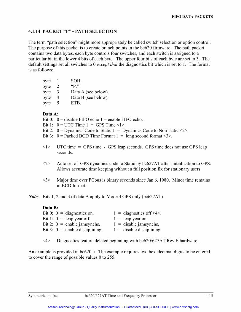
4.1.14 PACKET “P” - PATH SELECTION
The term “path selection” might more appropriately be called switch selection or option control.The purpose of this packet is to create branch points in the bc620 firmware. The path packetcontains two data bytes, each byte controls four switches, and each switch is assigned to aparticular bit in the lower 4 bits of each byte. The upper four bits of each byte are set to 3. Thedefault settings set all switches to 0 except that the diagnostics bit which is set to 1. The formatis as follows:
byte 1 SOH.byte 2 “P.”byte 3 Data A (see below).byte 4 Data B (see below).byte 5 ETB.
Data A:Bit 0: 0 = disable FIFO echo 1 = enable FIFO echo.Bit 1: 0 = UTC Time 1 = GPS Time <1>.Bit 2: 0 = Dynamics Code to Static 1 = Dynamics Code to Non-static <2>.Bit 3: 0 = Packed BCD Time Format 1 = long second format <3>.
<1> UTC time = GPS time - GPS leap seconds. GPS time does not use GPS leapseconds.
<2> Auto set of GPS dynamics code to Static by bc627AT after initialization to GPS. Allows accurate time keeping without a full position fix for stationary users.
<3> Major time over PCbus is binary seconds since Jan 6, 1980. Minor time remainsin BCD format.
Note: Bits 1, 2 and 3 of data A apply to Mode 4 GPS only (bc627AT).
Data B:Bit 0: 0 = diagnostics on. 1 = diagnostics off <4>.Bit 1: 0 = leap year off. 1 = leap year on.Bit 2: 0 = enable jamsynchs. 1 = disable jamsynchs.Bit 3: 0 = enable disciplining. 1 = disable disciplining.
<4> Diagnostics feature deleted beginning with bc620/627AT Rev E hardware .
An example is provided in bc620.c. The example requires two hexadecimal digits to be enteredto cover the range of possible values 0 to 255.
Artisan Technology Group - Quality Instrumentation ... Guaranteed | (888) 88-SOURCE | www.artisantg.com
CHAPTER FOUR
4-16 bc620/627AT Time and Frequency Processor Symmetricom, Inc.
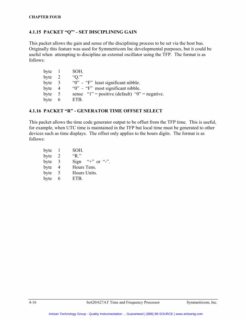
4.1.15 PACKET “Q”' - SET DISCIPLINING GAIN
This packet allows the gain and sense of the disciplining process to be set via the host bus. Originally this feature was used for Symmetricom Inc developmental purposes, but it could beuseful when attempting to discipline an external oscillator using the TFP. The format is asfollows:
byte 1 SOH.byte 2 “Q.”'byte 3 “0” - “F” least significant nibble.byte 4 “0” - “F” most significant nibble.byte 5 sense “1” = positive (default) “0” = negative.byte 6 ETB.
4.1.16 PACKET “R” - GENERATOR TIME OFFSET SELECT
This packet allows the time code generator output to be offset from the TFP time. This is useful,for example, when UTC time is maintained in the TFP but local time must be generated to otherdevices such as time displays. The offset only applies to the hours digits. The format is asfollows:
byte 1 SOH.byte 2 “R.”byte 3 Sign “+” or “-”.byte 4 Hours Tens.byte 5 Hours Units.byte 6 ETB.
Artisan Technology Group - Quality Instrumentation ... Guaranteed | (888) 88-SOURCE | www.artisantg.com
Symmetricom, Inc. bc620/627AT Time and Frequency Processor 5-1
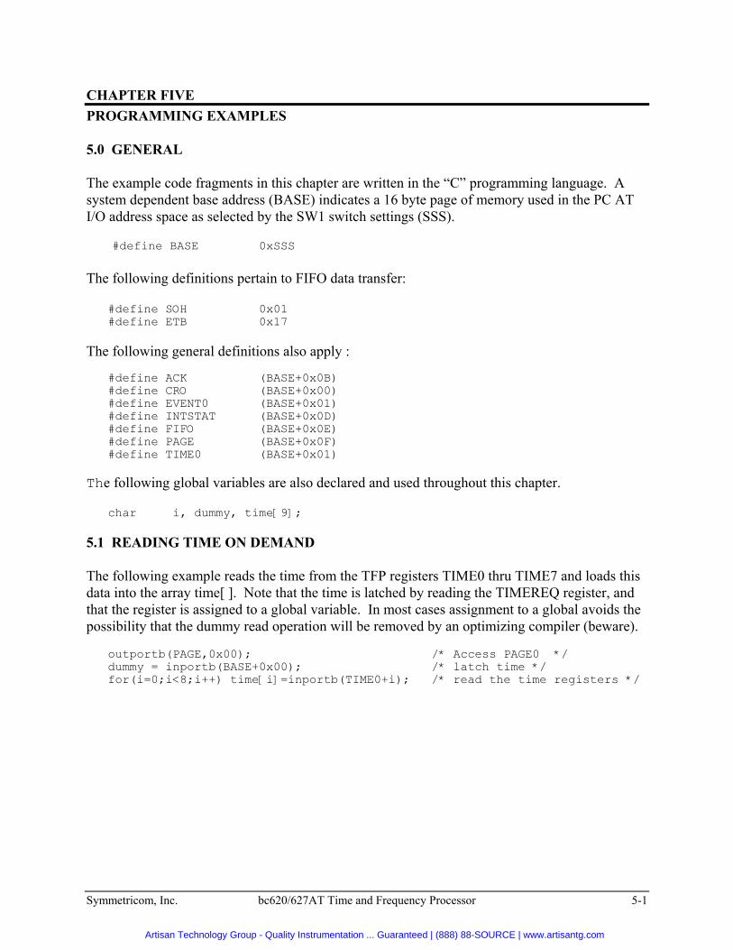
CHAPTER FIVEPROGRAMMING EXAMPLES
5.0 GENERAL
The example code fragments in this chapter are written in the “C” programming language. Asystem dependent base address (BASE) indicates a 16 byte page of memory used in the PC ATI/O address space as selected by the SW1 switch settings (SSS).
#define BASE 0xSSS
The following definitions pertain to FIFO data transfer:
#define SOH 0x01 #define ETB 0x17
The following general definitions also apply :
#define ACK (BASE+0x0B) #define CRO (BASE+0x00) #define EVENT0 (BASE+0x01) #define INTSTAT (BASE+0x0D) #define FIFO (BASE+0x0E) #define PAGE (BASE+0x0F) #define TIME0 (BASE+0x01)
The following global variables are also declared and used throughout this chapter.
char i, dummy, time[9];
5.1 READING TIME ON DEMAND
The following example reads the time from the TFP registers TIME0 thru TIME7 and loads thisdata into the array time[ ]. Note that the time is latched by reading the TIMEREQ register, andthat the register is assigned to a global variable. In most cases assignment to a global avoids thepossibility that the dummy read operation will be removed by an optimizing compiler (beware).
outportb(PAGE,0x00); /* Access PAGE0 */ dummy = inportb(BASE+0x00); /* latch time */ for(i=0;i<8;i++) time[i]=inportb(TIME0+i); /* read the time registers */
Artisan Technology Group - Quality Instrumentation ... Guaranteed | (888) 88-SOURCE | www.artisantg.com
CHAPTER FIVE
5-2 bc620/627AT Time and Frequency Processor Symmetricom, Inc.
5.2 EXTERNAL EVENT TIME CAPTURE
This example sets up the TFP event capture to occur on a rising edge. The time capture lockoutmechanism is also used.
/* Initialize TFP Event Hardware */
outportb(PAGE, 0x01); /* Switch to PAGE1 */ outportb(CR0, 0x09); /* enable event and lockout */ outportb(INTSTAT, 0x01); /* clear event INTSTAT bit */
/* Wait for Event and Process Data */
while(!(inportb(INTSTAT) & 0x01)); /* wait for event to occur */ for(i=0; i<9; i++) /* read event time */ time[i] = inportb(EVENT0+i); dummy = inportb(BASE+0x0A); /* release capture lockout */ outportb(INTSTAT, 0x01); /* clear event INTSTAT bit */
5.3 PROGRAM PERIODIC FREQUENCY OF 1000 Hz
This example uses a generalized send_packet( ) function to program a 1000 Hz output periodicsynchronized to the TFP 1pps epoch.
void send_packet(char *charptr) outportb(FIFO, SOH );
while(*charptr) outportb(FIFO, *charptr++ ); /* load body of packet*/
outportb(FIFO, ETB);outportb(ACK, 0x81); /* command TFP & clear ACK */while(!(inportb(ACK) & 0x01)); /* wait for TFP acknowledge */
/* Code Fragment which sets Periodic */
send_packet("F500630063"); /* 0x0063 = 99 = (100-1) */
5.4 SET MODE 1 AND THE MAJOR TIME
This example selects the free running mode and sets the TFP major time using the “B” packet.
send_packet("A1"); /* select mode 1 */ outportb(INTSTAT, 0x08); /* clear INTSTAT 1 PPS bit */ while(!(inportb(INTSTAT) & 0x08)); /* wait for 1 PPS */ send_packet("B123112233"); /* set the days thru seconds */
Artisan Technology Group - Quality Instrumentation ... Guaranteed | (888) 88-SOURCE | www.artisantg.com
PROGRAMMING EXAMPLES
Symmetricom, Inc. bc620AT Time and Frequency Processor 5-3
5.5 SELECT MODE 0 (IRIG B) AND ADVANCE TFP 2.5 MILLISECONDS
The following code fragment selects the mode, time code, and offset. The last “P” packet is usedto disable jamsynchs since the required offset is larger than 990 microseconds. See the “G”packet description for additional details on the jamsynch function.
send_packet("A0"); /* select mode 0 */ send_packet("HB"); /* select IRIG B time code */ send_packet("G+0025000"); /* advance 2.5 milliseconds */ send_packet("P04"); /* disable jamsynchs */
Artisan Technology Group - Quality Instrumentation ... Guaranteed | (888) 88-SOURCE | www.artisantg.com

CHAPTER FIVE
5-4 bc620/627AT Time and Frequency Processor Symmetricom, Inc.
This Page Intentionally Left Blank
Artisan Technology Group - Quality Instrumentation ... Guaranteed | (888) 88-SOURCE | www.artisantg.com
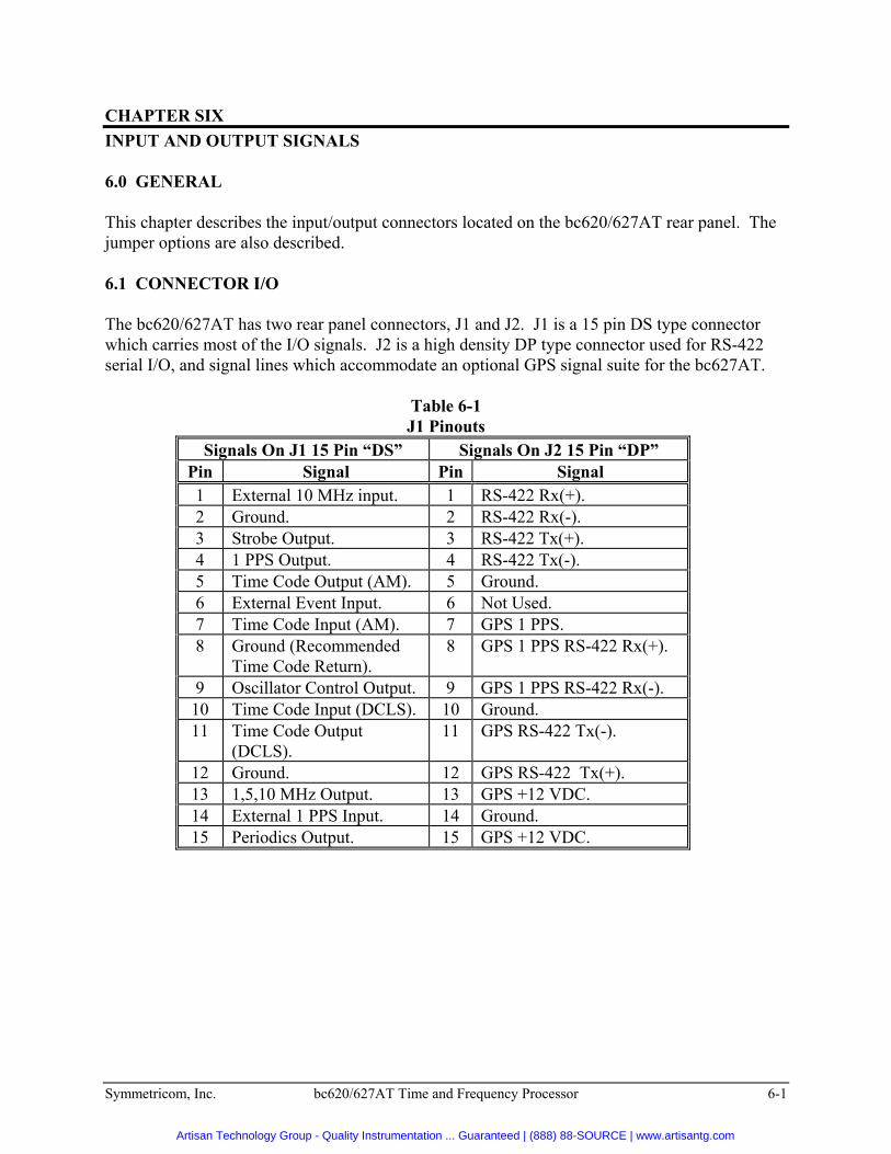
Symmetricom, Inc. bc620/627AT Time and Frequency Processor 6-1
CHAPTER SIXINPUT AND OUTPUT SIGNALS
6.0 GENERAL
This chapter describes the input/output connectors located on the bc620/627AT rear panel. Thejumper options are also described.
6.1 CONNECTOR I/O
The bc620/627AT has two rear panel connectors, J1 and J2. J1 is a 15 pin DS type connectorwhich carries most of the I/O signals. J2 is a high density DP type connector used for RS-422serial I/O, and signal lines which accommodate an optional GPS signal suite for the bc627AT.
Table 6-1J1 Pinouts
Signals On J1 15 Pin “DS” Signals On J2 15 Pin “DP”Pin Signal Pin Signal1 External 10 MHz input. 1 RS-422 Rx(+).2 Ground. 2 RS-422 Rx(-).3 Strobe Output. 3 RS-422 Tx(+).4 1 PPS Output. 4 RS-422 Tx(-).5 Time Code Output (AM). 5 Ground.6 External Event Input. 6 Not Used.7 Time Code Input (AM). 7 GPS 1 PPS.8 Ground (Recommended
Time Code Return).8 GPS 1 PPS RS-422 Rx(+).
9 Oscillator Control Output. 9 GPS 1 PPS RS-422 Rx(-).10 Time Code Input (DCLS). 10 Ground.11 Time Code Output
(DCLS).11 GPS RS-422 Tx(-).
12 Ground. 12 GPS RS-422 Tx(+).13 1,5,10 MHz Output. 13 GPS +12 VDC.14 External 1 PPS Input. 14 Ground.15 Periodics Output. 15 GPS +12 VDC.
Artisan Technology Group - Quality Instrumentation ... Guaranteed | (888) 88-SOURCE | www.artisantg.com

CHAPTER SIX
6-2 bc620/627AT Time and Frequency Processor Symmetricom, Inc.
6.2 JUMPER SELECTIONS
Refer to Figure 1-1 to locate the Jumpers described below.
Table 6-2JP1 Jumper Positions for PC AT InterruptJP1 Position PC at Interrupt
1 to 2 IRQ153 to 4 IRQ145 to 6 IRQ127 to 8 IRQ119 to 10 IRQ1011 to 12 IRQ913 to 14 IRQ715 to 16 IRQ617 to 18 IRQ519 to 20 IRQ421 to 22 IRQ3
* 22 to 23 No IRQ
Table 6-3JP2 Jumper Positions for RS-422 RX 100 OHM Termination
JP2 Position RS-422 Rx 100 ΩTermination
* 1 to 2 Terminated.3 to 4 No Termination.
*Indicates factory default position.
Artisan Technology Group - Quality Instrumentation ... Guaranteed | (888) 88-SOURCE | www.artisantg.com
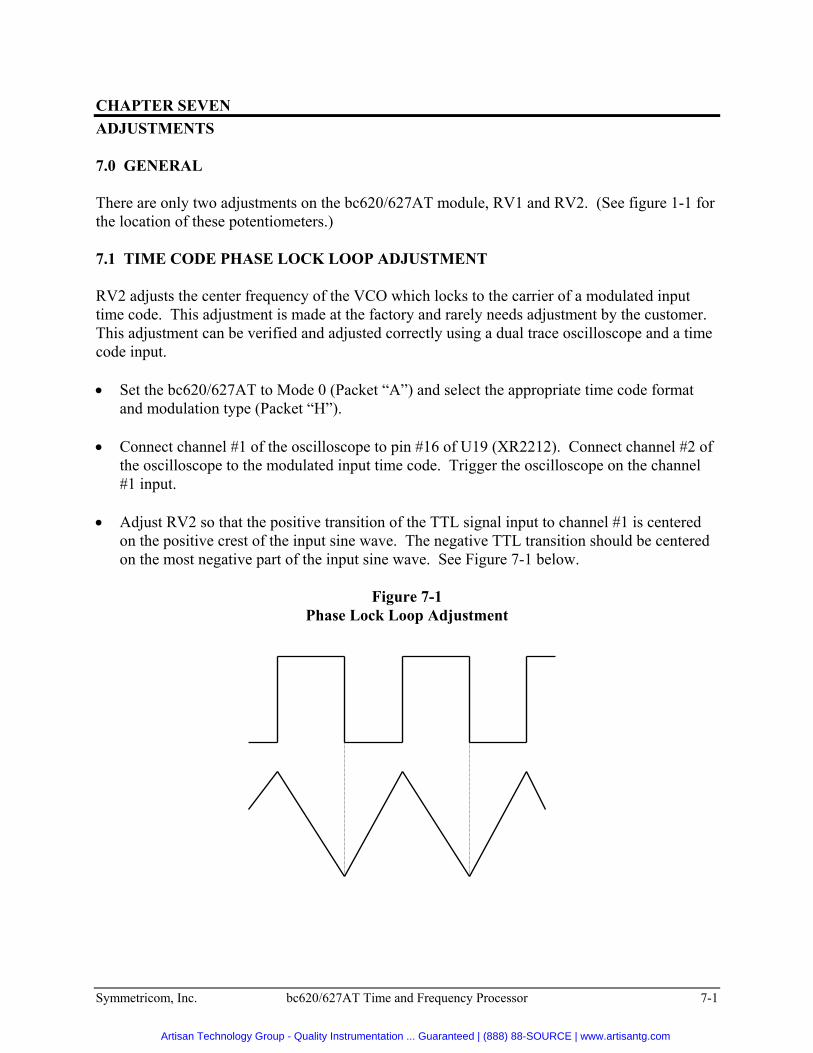
Symmetricom, Inc. bc620/627AT Time and Frequency Processor 7-1
CHAPTER SEVENADJUSTMENTS
7.0 GENERAL
There are only two adjustments on the bc620/627AT module, RV1 and RV2. (See figure 1-1 forthe location of these potentiometers.)
7.1 TIME CODE PHASE LOCK LOOP ADJUSTMENT
RV2 adjusts the center frequency of the VCO which locks to the carrier of a modulated inputtime code. This adjustment is made at the factory and rarely needs adjustment by the customer.This adjustment can be verified and adjusted correctly using a dual trace oscilloscope and a timecode input.
• Set the bc620/627AT to Mode 0 (Packet “A”) and select the appropriate time code formatand modulation type (Packet “H”).
• Connect channel #1 of the oscilloscope to pin #16 of U19 (XR2212). Connect channel #2 of
the oscilloscope to the modulated input time code. Trigger the oscilloscope on the channel#1 input.
• Adjust RV2 so that the positive transition of the TTL signal input to channel #1 is centered
on the positive crest of the input sine wave. The negative TTL transition should be centeredon the most negative part of the input sine wave. See Figure 7-1 below.
Figure 7-1Phase Lock Loop Adjustment
Artisan Technology Group - Quality Instrumentation ... Guaranteed | (888) 88-SOURCE | www.artisantg.com

CHAPTER SEVEN
7-2 bc620/627AT Time and Frequency Processor Symmetricom, Inc.
7.2 TIME CODE OUTPUT AMPLITUDE ADJUSTMENT
RV1 adjusts the amplitude of the modulated IRIG B output time code. A value of one volt RMSis common as is three volts peak-to-peak on the high cycles. Adjust this value to suit theequipment being driven. The range is zero to twenty-four volts peak-to-peak.
Artisan Technology Group - Quality Instrumentation ... Guaranteed | (888) 88-SOURCE | www.artisantg.com
Symmetricom, Inc. bc620/627AT Time and Frequency Processor A-1
APPENDIX AIRIG TIME CODE FORMAT
A.0 GENERAL
The widespread use of coded timing signals to assist in the correlation of intercept and test databegan in the early 1950’s. These signals can be decoded in real time to indicate the current Timeof Day (TOD) or recorded along with intercept/test data on magnetic tape recorders for postprocessing and time correlation.
Hundreds of time code formats were developed - one for each agency involved. During the early1960's the InterRange Instrumentation Group (IRIG) promoted a series of “standard” time codeformats now loosely referred to as “IRIG Time Codes.” The bc620/627AT decodes the mostwidely used format, IRIG B, as well as IRIG A. Figure A-1 illustrates a frame of IRIG timecode.
Artisan Technology Group - Quality Instrumentation ... Guaranteed | (888) 88-SOURCE | www.artisantg.com

APPENDIX A
A-2 bc620/627AT Time and Frequency Processor Symmetricom, Inc.
Figure A-1IRIG Time Code Frame
Artisan Technology Group - Quality Instrumentation ... Guaranteed | (888) 88-SOURCE | www.artisantg.com

SYMMETRICOM TIMING TEST & MEASUREMENT
3750 Westwind Blvd. Santa Rosa, California95403 USAtel : 707-528-1230fax : [email protected]
For more information about the complete range of Quality Timing Products from theSymmetricom Group of Companies, call 1-800-544-0233 in the US and Canada.
Or visit our site on the world wide web at http://www.symmetricom.comfor continuously updated product specifications, news and information.
Artisan Technology Group - Quality Instrumentation ... Guaranteed | (888) 88-SOURCE | www.artisantg.com