band theory of solids in isolated atoms the electrons are arranged in energy levels
TRANSCRIPT

Band Theory of Solids
In isolated atoms the electrons are arranged in energy levels
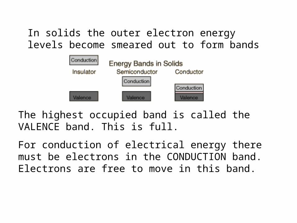
In solids the outer electron energy levels become smeared out to form bands
The highest occupied band is called the VALENCE band. This is full.
For conduction of electrical energy there must be electrons in the CONDUCTION band. Electrons are free to move in this band.

Insulators : There is a big energy gap between the valence and conduction band. Examples are plastics, paper …..
Conductors : There is an overlap between the valence and conduction band hence electrons are free to move about. Examples are copper, lead ….
Semiconductors : There is a small energy gap between the two bands. Thermal excitation is sufficient to move electrons from the valence to conduction band. Examples are silicon ,germanium….

When a conductor is heated its resistance increases ; The atoms vibrate more and the electrons find it more difficult to move through the conductor.
R
T
R
T
But in a semiconductor the resistance decreases with an increase in temperature. Electrons can be excited up to the conduction band. Conductivity increases

Doping
This is the replacement of a silicon atom in the crystal structure with a different atom. Typically 1 atom per 100 million silicon atoms is replaced. This changes the electrical properties.
Silicon is in group 4 of the periodic table. It has 4 valence electrons.
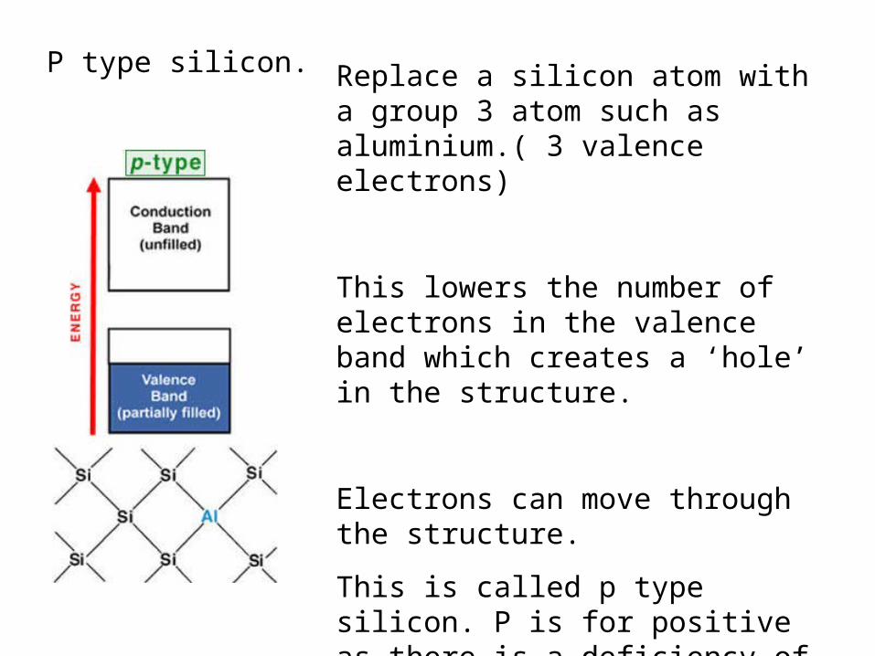
P type silicon. Replace a silicon atom with a group 3 atom such as aluminium.( 3 valence electrons)
This lowers the number of electrons in the valence band which creates a ‘hole’ in the structure.
Electrons can move through the structure.
This is called p type silicon. P is for positive as there is a deficiency of electrons.

N type
Replace a silicon atom with a group 5 atom such as phosphorous ( 5 valence electrons )
The extra electron introduced here goes into the conduction band as the valence band is full.
This is n type silicon.N for negative as ‘additional ‘ electrons have been introduced into the structure.

pn junction or diodeTo be forward biased ( current flows ) the p type must be connected to the positive terminal of the power supply.

pn junction
Electrons flow from the negative terminal of the battery to the n-type semiconductor, where they occupy the conduction band.
The electrons then move into the conduction band of the p-type (there is a potential barrier here that must be overcome) semiconductor and fall into the valence band. The excess energy is released as heat energy.
Electrons then move through wire.

Electrons do not flow from the p type to the n type and so a pn junction can be used as a rectifier. This allows current to flow through it in one direction and can be used to turn a.c to d.c.
There is actually a small reverse flow current of the order of micro amps but compared with the current flowing from n to p this is negligible.

LEDsElectrons flow from the negative terminal of the battery to the n-type semiconductor, where they occupy the conduction band.
The electrons then move into the conduction band of the p-type semiconductor and fall into the valence band this releases energy in the form of light.
The electrons then move through the wire back to the positive terminal of the battery, and they re-circulate.

The energy gap can be altered in the pn junction by adding different impurities. The bigger the energy gap the bigger the frequency of light emitted.
We will look at this in unit 3

Photovoltaic cells
These are like leds in reverse.
Photons of light enter the cell
An electron is ejected from the valence band in the p type producing a ‘hole’. Charges can flow.
This electron moves up to the conduction band
The electron moves to the conduction band of the n type silicon.
If the cell is connected to a load the electrons will flow around the external circuit.

The base of the triangle is the p type
The more photons of light that enter the cell the more electrons are released and the greater the potential difference.
The p type becomes the positive end and the n type the negative end of the ‘power supply’