aw series - nordson
TRANSCRIPT
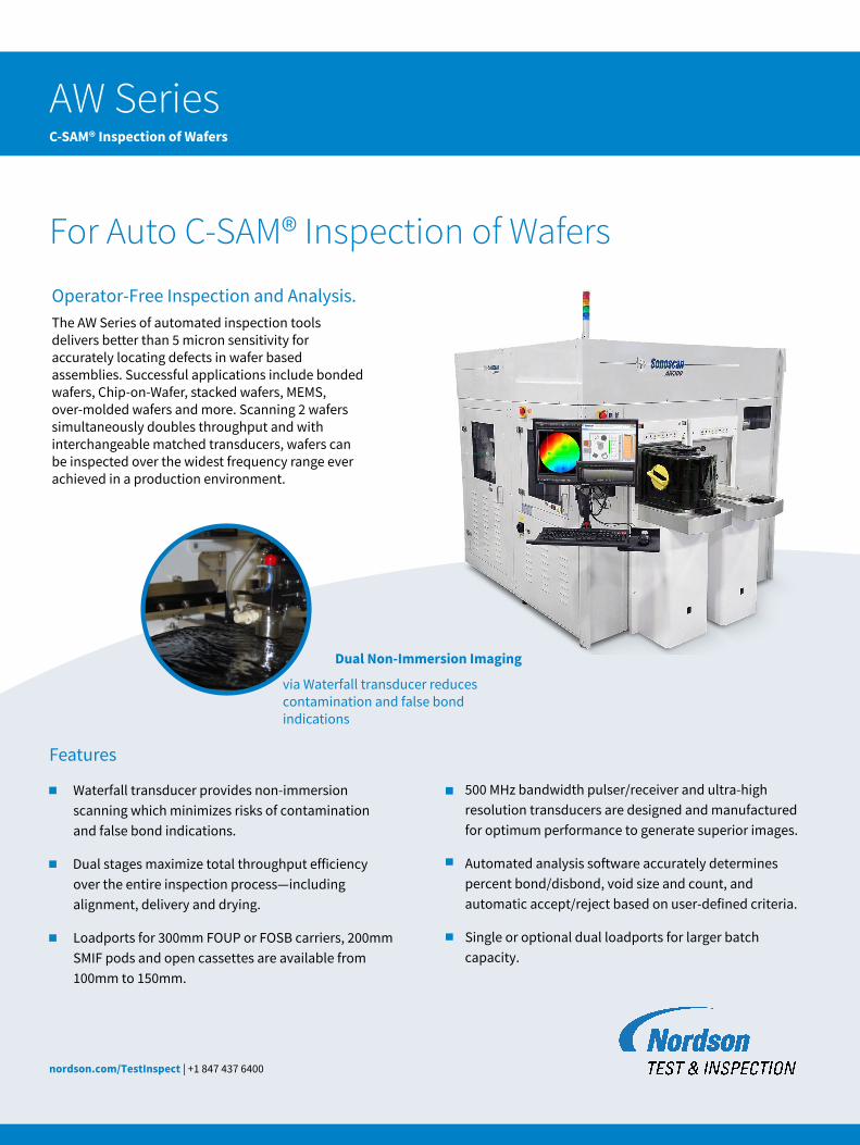
Operator-Free Inspection and Analysis.The AW Series of automated inspection tools delivers better than 5 micron sensitivity for accurately locating defects in wafer based assemblies. Successful applications include bonded wafers, Chip-on-Wafer, stacked wafers, MEMS, over-molded wafers and more. Scanning 2 wafers simultaneously doubles throughput and with interchangeable matched transducers, wafers can be inspected over the widest frequency range ever achieved in a production environment.
Features
Waterfall transducer provides non-immersion scanning which minimizes risks of contamination and false bond indications.
Dual stages maximize total throughput efficiency over the entire inspection process—including alignment, delivery and drying.
Loadports for 300mm FOUP or FOSB carriers, 200mm SMIF pods and open cassettes are available from 100mm to 150mm.
AW Series C-SAM® Inspection of Wafers
For Auto C-SAM® Inspection of Wafers
Dual Non-Immersion Imaging
via Waterfall transducer reduces contamination and false bond indications
500 MHz bandwidth pulser/receiver and ultra-high resolution transducers are designed and manufactured for optimum performance to generate superior images.
Automated analysis software accurately determines percent bond/disbond, void size and count, and automatic accept/reject based on user-defined criteria.
Single or optional dual loadports for larger batch capacity.
nordson.com/TestInspect | +1 847 437 6400

Bonded WaferEvaluating the bond quality in wafer pairs can uncover delaminated and voided regions which can lead to yield loss. White areas indicate voids and delaminations detected between wafers.
The AW Series delivers fully automated inspection, is SECS/GEM compliant and can be customized to specified requirements.
Applications & Technology
MEMS - Wafer Cavity Seal AnalysisMEMS cavity seal integrity is vital for proper operation. A thin or breached seal of the hermetic cavity can cause a reliability issue. Inspects seals for leaks and proper widths and improves product reliability.
Unpolished Bare WaferSave valuable process tool time by pre-screening for pinholes, scratches and bubble flaws that may not be visible on the surface.
MEMS - Bonded WaferDelaminations and voids can compromise the hermeticity of these devices. The regularly spaced features are intentional air cavities that contain the actual MEMS devices. The remaining red areas are defects.
SSL LED - WaferThe quality of the bond between layers of an SSL LED wafer will determine the yield of that wafer and the number of usable die from it. Improper bonding between layers within this SSL LED wafer is indicated by the red/yellow areas.
Wafer 3D ContourMeasure the global flatness of a wafer with the AW Acoustic Surface Flatness (ASF) technique.
Wafer Sizes from 100 - 300mmThe AW Series is capable of scanning multiple sized wafers.
100mm
125mm
150mm
200mm
300mm
Advanced RoboticsPrecise wafer positioning using the state-of-the-art 5 axis robot.
Flexible Wafer ChucksAvailable for 100 - 300mm wafers. Shown here are dual 200/300mm wafers stages.
Single or Dual LoadportsStandard BOLTS compatible load ports can be mixed for flexible configurations. For example, a FOUP and SMIF pod.
Digital Image Analysis (DIA)Advanced image analysis provides automated defect detection.
Dual Scanning MechanismDouble throughput with dual scan stages and carrier-to-carrier handling.
Waterfall TransducerDelivers fast scanning without requiring immersion. Ideal for production scanning and preventing contamination.
AW Series C-SAM® Inspection of Wafers

Optional Features
• Heater for water temperature stability and consistency
• ISO5 (Class 100) clean room compatible
• Acoustic Surface Flatness (ASF)
• MEMS - Wafer Cavity Seal Analysis (CSA)
• Chip Analysis Module
• KLARF and custom die mapping outputs
• Thickness Measurement Module
• Wafer OCR
• GEM Compliant SECS-II interface complies to SEMI E5, E30 and E37/E37.1 plus SEMI E39, E40, E87, E90 and E94
• OHT (Over Head Transport) with SEMI E84 Interface
Facility Requirements
• Power: 200V to 240V AC, 30A, single phase, 50/60 Hz
• Air: 1200 L/min (42.4 cfm) @ 0.62 MPa (90psi) of clean dry compressed air or nitrogen peak usage, 140 L/min (5 cfm) continuous
• DI Water: Pressure regulated to 1.4 – 2.0 bar (20 - 30psi) @ 4 L/min (1 US gal/min)Recommended SEMI F63.
• Dimensions: AIM: L 0.91 x W 1.73 x H 1.73 m (L 36 x W 68 x H 68 in.) Acoustic Imaging Module.
• EFEM: Equipment Front End Module. L 1.40 x W 1.73 x H 1.73 m (L 55 x W 68 x H 68 in.)
Standard Features
• Fully automated wafer analysis functions with two scanning stages
• Time Domain Pulse-Echo Modes include: A-Scan, B-Scan, C-Scan, Surface Scan, Interface Scan, Bulk Scan and Loss of Back Echo (LOBE)
• Wafer Analysis Package: Automated wafer bond analysis software for percent bond/no-bond, quantifies voids and has selectable accept/reject levels
• Sonolytics with PolyGate technology for Windows® 7 64-bit
Data Acquisition
• 500 MHz Bandwidth Pulser/Receiver for transducers from 100 to 400 MHz
• Transducers available from 5 to 400 MHz, typically >100 MHz used for wafer analysis
• Digital gating from 1 to 10,000nsec
• Acoustic Impedance Polarity Detector (AIPD)™ (Ref. U.S. Patent 4,866,986) simultaneously displays both polarity (i.e., phase) and amplitude information
• 95 dB Gain - selectable in 0.5 dB steps
• Dual display of digital waveform for A-Scan and capture criteria
Additional Features
• Waterfall transducer coupling for non-immersion scanning with or without water temperature controller option
• Single use (Std.) or re-circulatingwater system available
• Loadports are available for FOUP and FOSB carriers, SMIF pods and cassettes
• ISO6 (Class 1000) clean room ready
• Designed for production environment
• Integrated drying system for water removal
• Digital Image Analysis (DIA) includes area fraction analysis (including Mil-Std-883, Method 2030), image enhancement, histogram, and pixel amplitude analysis
• Integrated image archiving label function
AW Series C-SAM® Inspection of Wafers
Mechanical Features
• EFEM contains a high precision wafer handling robot with two staging areas for maximum productivity during the movement of wafers throughout the inspection, drying and alignment processes
• Wafer alignment function for pre-scan and prior to placement into the carrier
• Wafer count, missing and cross-slotted recognition for each carrier
• Configurable for multiple wafer sizes 100mm up to 300mm (12 in.)
• Repeatability x-y axis + 0.5 microns
• Digital servo high speed scanner linear motors for the fastest image acquisition time
• Inertially balanced, vibration-free dual (2) scanning mechanisms
• Up to 268 megapixels (16K) data resolution in multiple enhanced acquisition formats and various customizable color mappings
For more information, speak with your Nordson representative or contact your Nordson regional office
Equipment Sales and Service
Americas +1 847 437 6400 [email protected]
China +86 21 3866 9166 [email protected]
EMEA +44 1296 317800 [email protected]
Japan +81 3 3599 5920 [email protected]
Korea +82 31 462 9642 [email protected]
Singapore EA Region +65 6796 9500 [email protected]
Taiwan +886 2 2902 1860 [email protected]
www.nordson.com/TestInspectAW Series 4 page brochure 2022 V1Specifications subject to change without prior notice. Copyright © Nordson TEST & INSPECTION 2022Other products and company names mentioned are trademarks or tradenames of their respective companies. Nordson TEST & INSPECTION acoustic products are patent protected and covered by the patents listed at: https://www.nordson.com/en/divisions/sonoscan/about/patent-list