avr xmega a3u device datasheet - farnell element14 timer/counters with 4 output compare or input...
TRANSCRIPT
8/16-bit AtmelXMEGA A3UMicrocontroller
ATxmega256A3UATxmega192A3UATxmega128A3UATxmega64A3U
Preliminary
8386A–AVR–07/11
Features• High-performance, Low-power Atmel® AVR® XMEGA® 8/16-bit Microcontroller• Non-volatile Program and Data Memories
– 64K - 256KBytes of In-System Self-Programmable Flash– 4K - 8KBytes Boot Section– 2K - 4KBytes EEPROM– 4K - 16KBytes Internal SRAM
• Peripheral Features– Four-channel DMA Controller– Eight-channel Event System– Seven 16-bit Timer/Counters
Four Timer/Counters with 4 Output Compare or Input Capture channelsThree Timer/Counters with 2 Output Compare or Input Capture channelsHigh Resolution Extensions on all Timer/CountersAdvanced Waveform Extension on one Timer/Counter
– One USB device interfaceUSB 2.0 full speed (12Mbps) and low speed (1.5Mbps) device compliant32 Endpoints with full configuration flexibility
– Seven USARTs with IrDA support for one USART– AES and DES Crypto Engine– CRC-16 (CRC-CCITT) and CRC-32 (IEEE 802.3) Generator– Two Two-wire Interfaces with dual address match (I2C and SMBus compatible)– Three Serial Peripheral Interfaces (SPIs)– 16-bit Real Time Counter with Separate Oscillator– Two Eight-channel, 12-bit, 2MSPS Analog to Digital Converters– One Two-channel, 12-bit, 1MSPS Digital to Analog Converter– Four Analog Comparators with Window compare function, and current source
feature– External Interrupts on all General Purpose I/O pins– Programmable Watchdog Timer with Separate On-chip Ultra Low Power Oscillator– QTouch® library support
Capacitive touch buttons, sliders and wheelsUp to 64 sense channels
• Special Microcontroller Features– Power-on Reset and Programmable Brown-out Detection– Internal and External Clock Options with PLL– Programmable Multi-level Interrupt Controller – Five Sleep Modes– Programming and Debug Interfaces
JTAG (IEEE 1149.1 Compliant) Interface, including Boundary ScanPDI (Program and Debug Interface)
• I/O and Packages– 50 Programmable I/O Pins– 64-lead TQFP– 64-pad QFN
• Operating Voltage– 1.6 – 3.6V
• Operating Frequency– 0 – 12MHz from 1.6V– 0 – 32MHz from 2.7V
Typical Applications
• Industrial control • Climate control • Low power battery applications
• Factory automation • RF and ZigBee • Power tools
• Building control • USB connectivity • HVAC
• Board control • Sensor control • Utility metering
• White goods • Optical • Medical applications
XMEGA A3U
1. Ordering Information
Notes: 1. This device can also be supplied in wafer form. Please contact your local Atmel sales office for detailed ordering information.2. Pb-free packaging, complies to the European Directive for Restriction of Hazardous Substances (RoHS directive). Also Halide free and fully Green.3. For packaging information, see ”Errata” on page 109
Ordering Code Flash (Bytes) EEPROM (Bytes) SRAM (Bytes) Speed (MHz) Power Supply Package(1)(2)(3) Temp
ATxmega256A3U-AU 256K + 8K 4K 16K
32 1.6 - 3.6V
64A
-40°C - 85°C
ATxmega192A3U-AU 192K + 8K 2K 16K
ATxmega128A3U-AU 128K + 8K 2K 8K
ATxmega64A3U-AU 64K + 4K 2K 4K
ATxmega256A3U-MH 256K + 8K 4K 16K
64M2ATxmega192A3U-MH 192K + 8K 2K 16K
ATxmega128A3U-MH 128K + 8K 2K 8K
ATxmega64A3U-MH 64K + 4K 2K 4K
Package Type
64A 64-lead, 14 x 14mm Body Size, 1.0mm Body Thickness, 0.8mm Lead Pitch, Thin Profile Plastic Quad Flat Package (TQFP)
64M2 64-Pad, 9 x 9 x 1.0mm Body, Lead Pitch 0.50mm, 7.65mm Exposed Pad, Quad Flat No-Lead Package (QFN)
28386A–AVR–07/11
XMEGA A3U
2. Pinout/Block Diagram
Figure 2-1. Block diagram and pinout
Note: 1. For full details on pinout and alternate pin functions refer to ”Pinout and Pin Functions” on page 51.
Power/GroundDigital functionAnalog function
Programming, debug, testOscillator/Crystal/ClockGeneral Purpose I/O
1
2
3
4
64 63 62 61 60 59 58
VCC
5
6
7
8
9
10
11
12
13
14
15
16
48
47
46
45
44
43
42
41
40
39
38
37
36
35
34
33
57 56 55 54 53 52 51 50 49
17 18 19 20 21 22 23 24 25 26 27 28 29 30 31 32
GN
D
GND
VC
C
AV
CC
GN
D
PB0
PB1
PB3
PB2
PB7
PB5
PB4
PB6
PA7
PA6
PA0
PA1
PA2
PA3
PA4
PA5R
ESET
/PD
I
PDI
PR0
PR1
VD
D
GN
D
PC0
PC1
PC2
PC3
PC4
PC5
PC6
PC7
PD0
PD1
PD2
PD3
PD4
PD5
PD6
PD7
VCC
GND
PE0
PE1
PE2
PE3
PE4
PE5
PE6
PE7
PF0
PF1
PF2
PF3
PF4
PF5
PF6
PF7
VDD
GND
Port R
EVENT ROUTING NETWORK
DATA BUS
DATA BUS
Port
A
ADC
AC0:1
Port
B
ADC
DAC
AC0:1
AREF
JTAG
AREF
DMA Controller
BUS matrix
SRAMFLASH
OCD Prog/DebugInterface
EEPROM
Event System Controller
Watchdog Timer
WatchdogOSC/CLK Control
Real TimeCounter
Interrupt Controller
Sleep Controller
ResetController
TEMPREF
VREF
Crypto / CRC
CPU
Port EPort DPort C
TC0:
1
USA
RT0
:1
TWI
SPI
TC0:
1
USA
RT0
:1
SPI
TC0:
1
USA
RT0
:1
TWI
IRC
OM
USB
Port F
TC0
USA
RT0
SPI
Power Supervision
38386A–AVR–07/11
XMEGA A3U
3. Overview
The Atmel® AVR® XMEGA® is a family of low power, high performance and peripheral rich 8/16-bit microcontrollers based on the AVR® enhanced RISC architecture. By executing instructionsin a single clock cycle, the AVR achieves throughputs CPU approaching 1 Million InstructionsPer Second (MIPS) per MHz allowing the system designer to optimize power consumption ver-sus processing speed.
Atmel AVR CPU combines a rich instruction set with 32 general purpose working registers. Allthe 32 registers are directly connected to the Arithmetic Logic Unit (ALU), allowing two indepen-dent registers to be accessed in one single instruction, executed in one clock cycle. Theresulting architecture is more code efficient while achieving throughputs many times faster thanconventional single-accumulator or CISC based microcontrollers.
The XMEGA A3U devices provide the following features: In-System Programmable Flash withRead-While-Write capabilities, Internal EEPROM and SRAM, four-channel DMA Controller,eight-channel Event System, Programmable Multi-level Interrupt Controller, 50 general purposeI/O Pins, 16-bit Real Time Counter, seven flexible 16-bit Timer/Counters with compare andPWM channels, one USB 2.0 full speed (12Mbps) Device Interface, seven USARTs, two TwoWire Serial Interfaces (TWIs), three Serial Peripheral Interfaces (SPIs), AES and DES cryptoengine, two 8-channel 12-bit ADCs with optional differential input with programmable gain, one2-channel 12-bit DACs, four analog comparators with window mode, programmable WatchdogTimer with separate Internal Oscillator, accurate internal oscillators with PLL and prescaler andprogrammable Brown-Out Detection.
The Program and Debug Interface (PDI), a fast 2-pin interface for programming and debugging,is available. The devices also have an IEEE std. 1149.1 compliant JTAG test interface, and thiscan also be used for On-chip Debug and programming.
All XMEGA devices have five software selectable power saving modes. The Idle mode stops theCPU while allowing the SRAM, DMA Controller, Event System, Interrupt Controller and allperipherals to continue functioning. The Power-down mode saves the SRAM and register con-tents but stops the oscillators, disabling all other functions until the next TWI or pin-changeinterrupt, or Reset. In Power-save mode, the asynchronous Real Time Counter continues to run,allowing the application to maintain a timer base while the rest of the device is sleeping. InStandby mode, the Crystal/Resonator Oscillator is kept running while the rest of the device issleeping. This allows very fast start-up from external crystal combined with low power consump-tion. In Extended Standby mode, both the main Oscillator and the Asynchronous Timer continueto run. To further reduce power consumption, the peripheral clock to each individual peripheralcan optionally be stopped in Active mode and Idle sleep mode.
Atmel offers a free QTouch® library for embedding capacitive touch buttons, sliders and wheelsfunctionality into AVR microcontrollers.
The device is manufactured using Atmel's high-density nonvolatile memory technology. The pro-gram Flash memory can be reprogrammed in-system through the PDI or JTAG. A Bootloaderrunning in the device can use any interface to download the application program to the Flashmemory. The Bootloader software in the Boot Flash section will continue to run while the Appli-cation Flash section is updated, providing true Read-While-Write operation. By combining an8/16-bit RISC CPU with In-System Self-Programmable Flash, the Atmel XMEGA A3U is a pow-erful microcontroller family that provides a highly flexible and cost effective solution forembedded applications.
48386A–AVR–07/11
XMEGA A3U
The XMEGA devices are supported with a full suite of program and system development toolsincluding: C compilers, macro assemblers, program debugger/simulators, programmers, andevaluation kits.
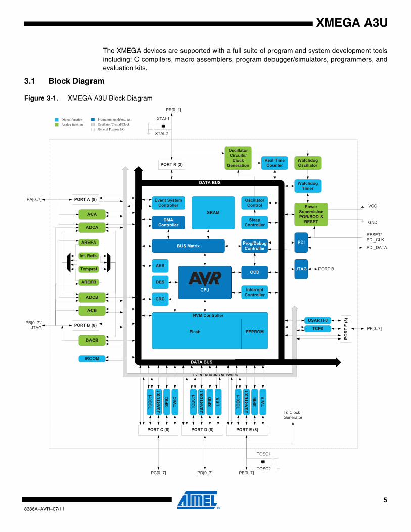
3.1 Block Diagram
Figure 3-1. XMEGA A3U Block Diagram
Power SupervisionPOR/BOD &
RESET
PORT A (8)
PORT B (8)
DMAController
SRAM
ADCA
ACA
DACB
ADCB
ACB
OCD
PDI
PA[0..7]
PB[0..7]/JTAG
Watchdog Timer
WatchdogOscillator
Interrupt Controller
DATA BUS
Prog/DebugController
VCC
GND
Oscillator Circuits/
Clock Generation
Oscillator Control
Real TimeCounter
Event System Controller
JTAG
AREFA
AREFB
PDI_DATA
RESET/PDI_CLK
PORT B
Sleep Controller
DES
CRC
PORT C (8)
PC[0..7]
TCC
0:1
USA
RTC
0:1
TWIC
SPIC
PD[0..7] PE[0..7]
PORT D (8)
TCD
0:1
USA
RTD
0:1
SPID
TCE0
:1
USA
RTE
0:1
TWIE
SPIE
PORT E (8)
AES
USB
PORT R (2)
XTAL1
XTAL2
PR[0..1]
DATA BUS
NVM Controller
MORPEEhsalF
IRCOM
BUS Matrix
CPU
TOSC1
TOSC2
TCF0
USARTF0
PF[0..7]
POR
T F
(8)
EVENT ROUTING NETWORK
To Clock Generator
Int. Refs.
Tempref
Digital functionAnalog function
Programming, debug, testOscillator/Crystal/ClockGeneral Purpose I/O
58386A–AVR–07/11
XMEGA A3U
4. Resources
A comprehensive set of development tools, application notes and datasheets are available fordownload on http://www.atmel.com/avr.
4.1 Recommended reading
• XMEGA® AU Manual
• XMEGA Application Notes
This device data sheet only contains part specific information with a short description of eachperipheral and module. The XMEGA AU Manual describes the modules and peripherals indepth. The XMEGA application notes contain example code and show applied use of the mod-ules and peripherals.
All documentations are available from www.atmel.com/avr.
5. Capacitive touch sensingThe Atmel® QTouch® Library provides a simple to use solution to realize touch sensitive inter-faces on most Atmel AVR® microcontrollers. The patented charge-transfer signal acquisitionoffers robust sensing and includes fully debounced reporting of touch keys and includes Adja-cent Key Suppression® (AKS™) technology for unambiguous detection of key events. TheQTouch Library includes support for the QTouch and QMatrix® acquisition methods.
Touch sensing can be added to any application by linking the appropriate Atmel QTouch Libraryfor the AVR Microcontroller. This is done by using a simple set of APIs to define the touch chan-nels and sensors, and then calling the touch sensing API’s to retrieve the channel informationand determine the touch sensor states.
The QTouch Library is FREE and downloadable from the Atmel website at the following location:www.atmel.com/qtouchlibrary. For implementation details and other information, refer to theAtmel QTouch Library User Guide - also available for download from the Atmel website.
68386A–AVR–07/11
XMEGA A3U
6. AVR CPU
6.1 Features
• 8/16-bit high performance AVR RISC Architecture– 142 instructions– Hardware multiplier
• 32x8-bit registers directly connected to the ALU• Stack in SRAM• Stack Pointer accessible in I/O memory space• Direct addressing of up to 16Mbytes of program and 16Mbytes of data memory• True 16/24-bit access to 16/24-bit I/O registers• Support for 8-, 16- and 32-bit Arithmetic• Configuration Change Protection of system critical features
6.2 Overview
The Atmel® AVR® XMEGA® devices use the 8/16-bit AVR CPU. The main function of the CPU isto execute the code and perform all calculations. The CPU is able to access memories, performcalculations, control peripherals, and execute the program from the FLASH memory. Interrupthandling is described in a separate section, refer to ”Interrupts and Programmable Multi-levelInterrupt Controller” on page 26.
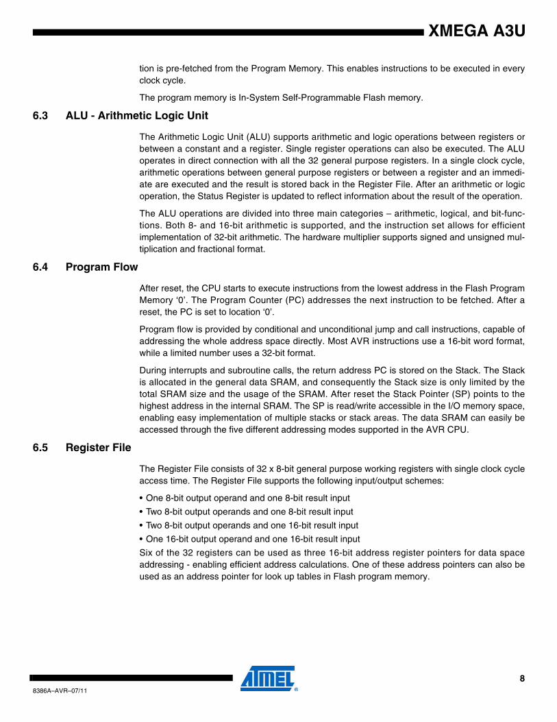
Figure 6-1 on page 7 shows the block diagram of the AVR CPU architecture.
Figure 6-1. Block Diagram of the AVR CPU architecture
In order to maximize performance and parallelism, the AVR uses a Harvard architecture withseparate memories and buses for program and data. Instructions in the program memory areexecuted with a single level pipelining. While one instruction is being executed, the next instruc-
78386A–AVR–07/11
XMEGA A3U
tion is pre-fetched from the Program Memory. This enables instructions to be executed in everyclock cycle.
The program memory is In-System Self-Programmable Flash memory.
6.3 ALU - Arithmetic Logic Unit
The Arithmetic Logic Unit (ALU) supports arithmetic and logic operations between registers orbetween a constant and a register. Single register operations can also be executed. The ALUoperates in direct connection with all the 32 general purpose registers. In a single clock cycle,arithmetic operations between general purpose registers or between a register and an immedi-ate are executed and the result is stored back in the Register File. After an arithmetic or logicoperation, the Status Register is updated to reflect information about the result of the operation.
The ALU operations are divided into three main categories – arithmetic, logical, and bit-func-tions. Both 8- and 16-bit arithmetic is supported, and the instruction set allows for efficientimplementation of 32-bit arithmetic. The hardware multiplier supports signed and unsigned mul-tiplication and fractional format.
6.4 Program Flow
After reset, the CPU starts to execute instructions from the lowest address in the Flash ProgramMemory ‘0’. The Program Counter (PC) addresses the next instruction to be fetched. After areset, the PC is set to location ‘0’.
Program flow is provided by conditional and unconditional jump and call instructions, capable ofaddressing the whole address space directly. Most AVR instructions use a 16-bit word format,while a limited number uses a 32-bit format.
During interrupts and subroutine calls, the return address PC is stored on the Stack. The Stackis allocated in the general data SRAM, and consequently the Stack size is only limited by thetotal SRAM size and the usage of the SRAM. After reset the Stack Pointer (SP) points to thehighest address in the internal SRAM. The SP is read/write accessible in the I/O memory space,enabling easy implementation of multiple stacks or stack areas. The data SRAM can easily beaccessed through the five different addressing modes supported in the AVR CPU.
6.5 Register File
The Register File consists of 32 x 8-bit general purpose working registers with single clock cycleaccess time. The Register File supports the following input/output schemes:
• One 8-bit output operand and one 8-bit result input
• Two 8-bit output operands and one 8-bit result input
• Two 8-bit output operands and one 16-bit result input
• One 16-bit output operand and one 16-bit result input
Six of the 32 registers can be used as three 16-bit address register pointers for data spaceaddressing - enabling efficient address calculations. One of these address pointers can also beused as an address pointer for look up tables in Flash program memory.
88386A–AVR–07/11
XMEGA A3U
7. Memories
7.1 Features
• Flash Program Memory– One linear address space– In-System Programmable– Self-Programming and Bootloader support– Application Section for application code– Application Table Section for application code or data storage– Boot Section for application code or bootloader code– Separate read/write protection lock bits for all sections– CRC Generator support for CRC check of a selectable flash program memory section
• Data Memory– One linear address space– Single cycle access from CPU– SRAM– EEPROM
Byte and page accessibleOptional memory mapping for direct load and store
– I/O MemoryConfiguration and Status registers for all peripherals and modules16bit-accessible General Purpose Register for global variables or flags
– Bus arbitrationSafe and deterministic handling of priority between CPU, DMA Controller, and other bus masters
– Separate buses for SRAM, EEPROM, and I/O MemorySimultaneous bus access for CPU and DMA Controller
• Production Signature Row Memory for factory programmed data– ID for each microcontroller device type– Serial number for each device– Calibration bytes for factory calibrated peripherals
• User Signature Row– One flash page in size– Can be read and written from software– Content is kept after chip erase
7.2 Overview
The Atmel® AVR® architecture has two main memory spaces, the Program Memory and theData Memory. Executable code can only reside in the Program Memory, while data can bestored both in the Program Memory and the Data Memory. The Data Memory includes bothSRAM, and EEPROM Memory for nonvolatile data storage. All memory spaces are linear andrequire no memory bank switching.
The available memory size configurations are shown in ”Ordering Information” on page 2. Inaddition each device has a Flash memory signature rows for calibration data, device identifica-tion, serial number etc.
Non Volatile Memory (NVM) spaces can be locked for further write and read/write operations.This prevents unrestricted access to the application software.
98386A–AVR–07/11
XMEGA A3U
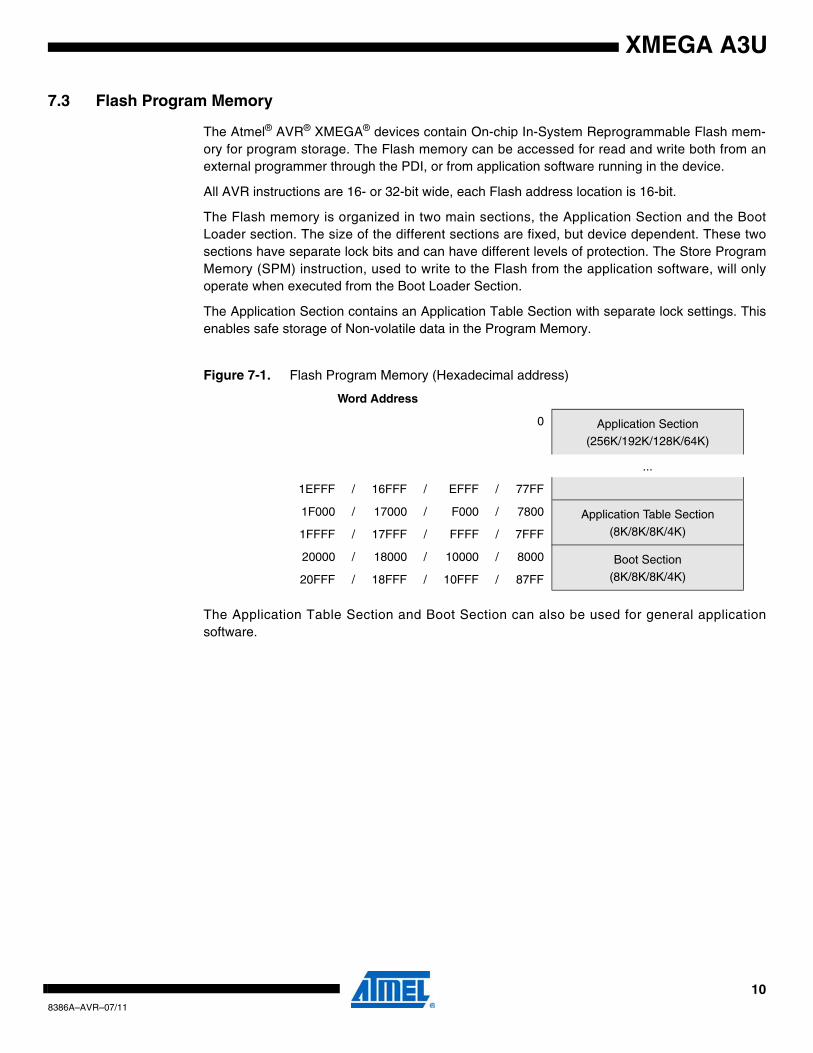
7.3 Flash Program Memory
The Atmel® AVR® XMEGA® devices contain On-chip In-System Reprogrammable Flash mem-ory for program storage. The Flash memory can be accessed for read and write both from anexternal programmer through the PDI, or from application software running in the device.
All AVR instructions are 16- or 32-bit wide, each Flash address location is 16-bit.
The Flash memory is organized in two main sections, the Application Section and the BootLoader section. The size of the different sections are fixed, but device dependent. These twosections have separate lock bits and can have different levels of protection. The Store ProgramMemory (SPM) instruction, used to write to the Flash from the application software, will onlyoperate when executed from the Boot Loader Section.
The Application Section contains an Application Table Section with separate lock settings. Thisenables safe storage of Non-volatile data in the Program Memory.
The Application Table Section and Boot Section can also be used for general applicationsoftware.
Figure 7-1. Flash Program Memory (Hexadecimal address)
Word Address
0 Application Section(256K/192K/128K/64K)
...
1EFFF / 16FFF / EFFF / 77FF
1F000 / 17000 / F000 / 7800 Application Table Section
(8K/8K/8K/4K)1FFFF / 17FFF / FFFF / 7FFF
20000 / 18000 / 10000 / 8000 Boot Section(8K/8K/8K/4K)20FFF / 18FFF / 10FFF / 87FF
108386A–AVR–07/11
XMEGA A3U
7.4 Data Memory
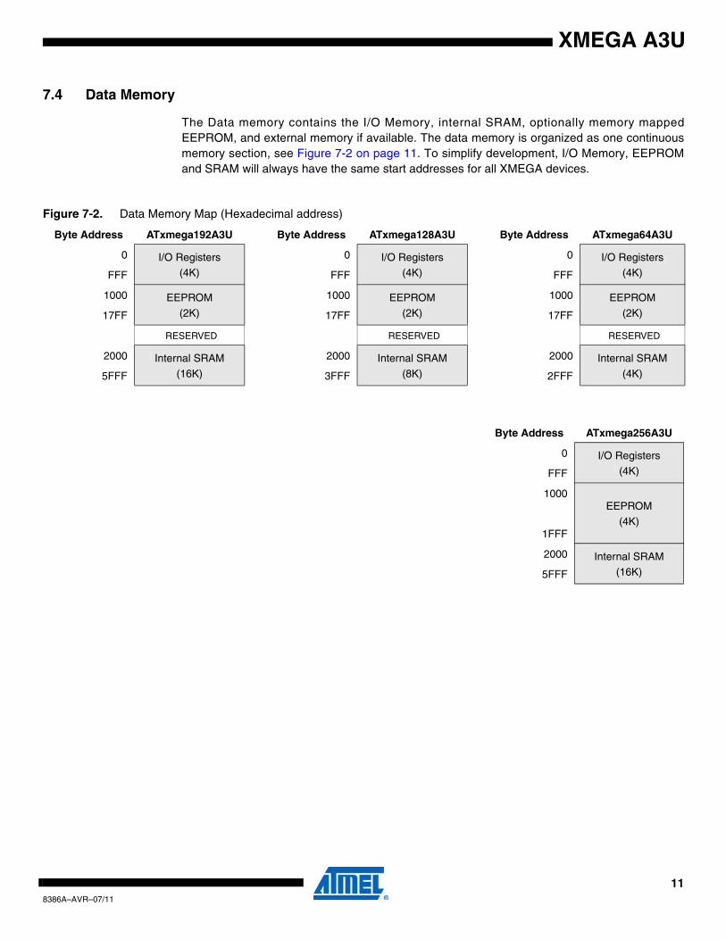
The Data memory contains the I/O Memory, internal SRAM, optionally memory mappedEEPROM, and external memory if available. The data memory is organized as one continuousmemory section, see Figure 7-2 on page 11. To simplify development, I/O Memory, EEPROMand SRAM will always have the same start addresses for all XMEGA devices.
Figure 7-2. Data Memory Map (Hexadecimal address)
Byte Address ATxmega192A3U Byte Address ATxmega128A3U Byte Address ATxmega64A3U
0 I/O Registers(4K)
0 I/O Registers(4K)
0 I/O Registers(4K)FFF FFF FFF
1000 EEPROM
(2K)
1000 EEPROM
(2K)
1000 EEPROM
(2K)17FF 17FF 17FF
RESERVED RESERVED RESERVED
2000 Internal SRAM
(16K)
2000 Internal SRAM
(8K)
2000 Internal SRAM
(4K)5FFF 3FFF 2FFF
Byte Address ATxmega256A3U
0 I/O Registers
(4K)FFF
1000EEPROM
(4K)1FFF
2000 Internal SRAM(16K)5FFF
118386A–AVR–07/11
XMEGA A3U
7.4.1 I/O Memory
The Status and configuration registers for peripherals and modules, including the CPU, areaddressable through I/O memory locations. All I/O locations can be accessed by the load(LD/LDS/LDD) and store (ST/STS/STD) instructions, which is used to transfer data between the32 registers in the Register File and the I/O memory. The IN and OUT instructions can addressI/O memory locations in the range 0x00 - 0x3F directly. In the address range 0x00 - 0x1F, sin-gle- cycle instructions for manipulation and checking of individual bits are available.
The I/O memory address for all peripherals and modules in XMEGA A3U is shown in the”Peripheral Module Address Map” on page 56.
7.4.2 SRAM Data Memory
The devices have internal SRAM memory for data storage.
7.4.3 EEPROM Data Memory
The devices have internal EEPROM memory for non-volatile data storage. It is addressableeither in a separate data space or it can be memory mapped into the normal data memoryspace. The EEPROM memory supports both byte and page access.
128386A–AVR–07/11
XMEGA A3U
7.5 Production Signature Row
The Production Signature Row is a separate memory section for factory programmed data. Itcontains calibration data for functions such as oscillators and analog modules.
The production signature row also contains an ID that identifies each microcontroller devicetype, and a serial number that is unique for each manufactured device. The device ID for theavailable devices is shown in Table 7-1 on page 13. The serial number consist of the productionLOT number, wafer number, and wafer coordinates for the device.
The production signature row can not be written or erased, but it can be read from both applica-tion software and external programming.
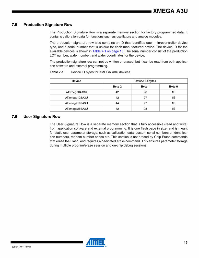
Table 7-1. Device ID bytes for XMEGA A3U devices.
7.6 User Signature Row
The User Signature Row is a separate memory section that is fully accessible (read and write)from application software and external programming. It is one flash page in size, and is meantfor static user parameter storage, such as calibration data, custom serial numbers or identifica-tion numbers, random number seeds etc. This section is not erased by Chip Erase commandsthat erase the Flash, and requires a dedicated erase command. This ensures parameter storageduring multiple program/erase session and on-chip debug sessions.
Device Device ID bytes
Byte 2 Byte 1 Byte 0
ATxmega64A3U 42 96 1E
ATxmega128A3U 42 97 1E
ATxmega192A3U 44 97 1E
ATxmega256A3U 42 98 1E
138386A–AVR–07/11

XMEGA A3U
7.7 Flash and EEPROM Page Size
The Flash Program Memory and EEPROM data memory are organized in pages. The pages areword accessible for the Flash and byte accessible for the EEPROM.
Table 7-2 on page 14 shows the Flash Program Memory organization. Flash write and eraseoperations are performed on one page at a time, while reading the Flash is done one byte at atime. For Flash access the Z-pointer (Z[m:n]) is used for addressing. The most significant bits inthe address (FPAGE) gives the page number and the least significant address bits (FWORD)gives the word in the page.
Table 7-2. Number of words and Pages in the Flash.
Table 7-3 on page 14 shows EEPROM memory organization for the XMEGA A3U devices.EEEPROM write and erase operations can be performed one page or one byte at a time, whilereading the EEPROM is done one byte at a time. For EEPROM access the NVM Address Regis-ter (ADDR[m:n]) is used for addressing. The most significant bits in the address (E2PAGE) givesthe page number and the least significant address bits (E2BYTE) gives the byte in the page.
Table 7-3. Number of bytes and Pages in the EEPROM.
Devices Flash Page Size FWORD FPAGE Application Boot
Size (words) Size No of Pages Size No of Pages
ATxmega64A3U 64K + 4K 128 Z[7:1] Z[16:8] 64K 256 4K 16
ATxmega128A3U 128K + 8K 256 Z[8:1] Z[17:9] 128K 256 8K 16
ATxmega192A3U 192K + 8K 256 Z[8:1] Z[18:9] 192K 384 8K 16
ATxmega256A3U 256K + 8K 256 Z[8:1] Z[18:9] 256K 512 8K 16
Devices EEPROM Page Size E2BYTE E2PAGE No of Pages
Size (Bytes)
ATxmega64A3U 2K 32 ADDR[4:0] ADDR[10:5] 64
ATxmega128A3U 2K 32 ADDR[4:0] ADDR[10:5] 64
ATxmega192A3U 2K 32 ADDR[4:0] ADDR[10:5] 64
ATxmega256A3U 4K 32 ADDR[4:0] ADDR[11:5] 128
148386A–AVR–07/11
XMEGA A3U
8. DMAC - Direct Memory Access Controller
8.1 Features
• The DMA Controller allows data transfers with minimal CPU intervention– from data memory to data memory– from data memory to peripheral– from peripheral to data memory– from peripheral to peripheral
• Four DMA Channels with separate– transfer triggers– interrupt vectors– addressing modes
• Programmable channel priority• From 1byte to 16Mbytes of data in a single transaction• Multiple addressing modes
– Static– Increment– Decrement
• Optional reload of source and destination address at the end of each– Burst– Block– Transaction
• Optional Interrupt on end of transaction• Optional connection to CRC Generator module for CRC on DMA data
8.2 Overview
The 4-channel Direct Memory Access (DMA) Controller can transfer data between memoriesand peripherals, and thus offload these tasks from the CPU. It enables high data transfer rateswith minimum CPU intervention, and frees up CPU time. The 4 DMA channels enable up to fourindependent and parallel transfers.
The DMA Controller can move data between SRAM and peripherals, between SRAM locationsand between peripheral registers directly. With access to all peripherals the DMA Controller canhandle automatic transfer of data to/from communication modules, as well as data retrieval fromADC conversions, or data transfer to or from port pins. The DMA Controller can also read frommemory mapped EEPROM.
Data transfers are done in continues bursts of 1, 2, 4 or 8bytes. They build block transfers ofconfigurable size from 1 to 64Kbytes. A repeat counter can be used to repeat each block trans-fer for single transactions up to 16Mbytes. Source and destination addressing can be static,incremental or decremental. Automatic reload of source and/or destination address can be doneafter each burst, block transfer, or when transaction is complete. Application software, peripher-als and events can trigger DMA transfers.
The four DMA channels have individual configuration and control settings. This include source,destination, transfer triggers and transaction sizes. They have individual interrupt settings. Inter-rupt requests can be generated both when a transaction is complete or if the DMA Controllerdetects an error on a DMA channel.
To allow for continuous transfers, two channels can be interlinked so that the second takes overthe transfer when the first is finished and vice versa.
158386A–AVR–07/11
XMEGA A3U
9. Event System9.1 Features
• System for direct peripheral to peripheral communication and signaling• Peripherals can directly send, receive and react to peripheral events
– CPU and DMA controller independent operation– 100% predictable signal timing– Short and guaranteed response time
• 8 Event Channels for up to 8 different and parallel signal routines and configurations• Events can be sent and/or used by most peripherals, clock system and software• Additional functions include
– Quadrature Decoders– Digital Filtering of I/O pin change
• Works in Active mode and Idle sleep mode
9.2 Overview
The Event System is system for direct peripheral to peripheral communication and signaling. Itenables the possibility for a change in one peripheral to automatically trigger actions in othersperipherals. It is designed for having a predictable system for short and guaranteed responsetime between peripherals. It is simple and powerful since it allows for autonomous peripheralcontrol and interaction without use of interrupts, CPU or DMA Controller resources. It alsoenables synchronized timing of actions in several peripheral modules.
The change in a peripheral is referred to as an event, and is it usually the same as the interruptconditions for the peripheral. These events can be directly passed to other peripherals using adedicated routing network called the Event Routing Network. How events are routed and usedby other peripherals is configured in software.
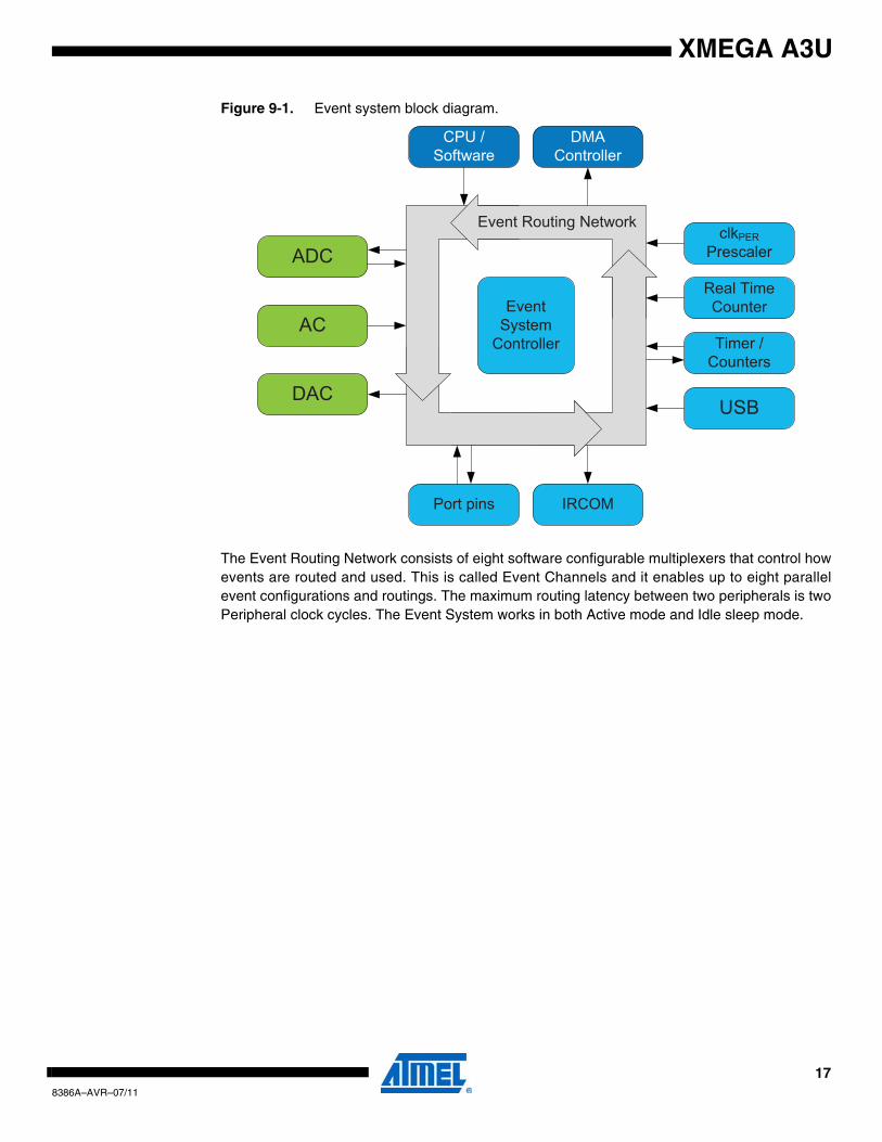
Figure 9-1 on page 17 shows a basic block diagram of all connected peripherals. The EventSystem can directly connect together Analog and Digital converters, Analog Comparators, I/Oports pins, the Real-time Counter, Timer/Counters, IR Communication Module (IRCOM), andUSB. It can also be used to trigger DMA transactions (DMA Controller). Events can also be gen-erated from software and the Peripheral Clock.
168386A–AVR–07/11
XMEGA A3U
Figure 9-1. Event system block diagram.
The Event Routing Network consists of eight software configurable multiplexers that control howevents are routed and used. This is called Event Channels and it enables up to eight parallelevent configurations and routings. The maximum routing latency between two peripherals is twoPeripheral clock cycles. The Event System works in both Active mode and Idle sleep mode.
DAC
Timer / Counters
USB
ADCReal Time Counter
Port pins
CPU / Software
DMAController
IRCOM
Event Routing Network
EventSystem
Controller
clkPERPrescaler
AC
178386A–AVR–07/11
XMEGA A3U
10. System Clock and Clock options
10.1 Features
• Fast start-up time• Safe run-time clock switching• Internal Oscillators:
– 32MHz run-time calibrated and tuneable oscillator– 2MHz run-time calibrated oscillator – 32.768kHz calibrated oscillator– 32kHz Ultra Low Power (ULP) oscillator with 1kHz output
• External clock options– 0.4 - 16MHz Crystal Oscillator– 32kHz Crystal Oscillator– External clock
• PLL with 20 - 128MHz output frequency– Internal and external clock options and 1 to 31x multiplication– Lock detector
• Clock Prescalers with 1 to 2048x division• Fast peripheral clocks running at 2 and 4 times the CPU clock frequency• Automatic Run-Time Calibration of internal oscillators• External oscillator and PLL lock failure detection with optional non maskable interrupt
10.2 Overview
The flexible clock system supports a large number of clock sources. It incorporates both accu-rate internal oscillators, and external crystal oscillators and resonator support. A high frequencyPhase Locked Loop (PLL) and clock prescalers can be used to generate a wide range of clockfrequencies. A calibration feature (DFLL) is available, and can be used for automatic runtimecalibration of the internal oscillators to remove frequency drift over voltage and temperate. AnOscillator Failure Monitor can be enabled to issue a Non-Maskable Interrupt and switch to inter-nal oscillator if the external oscillator or PLL fails.
When a reset occur, all clock sources except 32kHz Ultra Low Power oscillator are disabled.After reset, the device will always start up running from the 2MHz internal oscillator. During nor-mal operation, the System Clock source and prescalers can be changed from software at anytime.
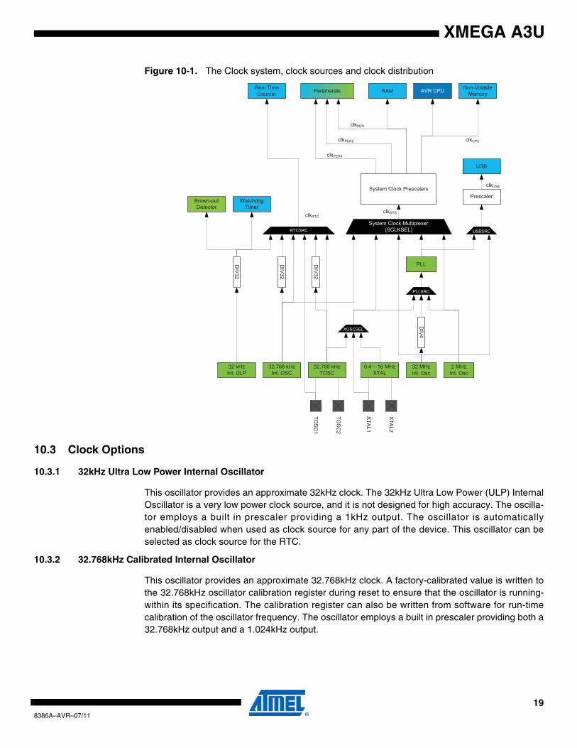
Figure 10-1 on page 19 presents the principal clock system in the XMEGA. All of the clocks donot need to be active at a given time. The clocks to the CPU and peripherals can be stoppedusing sleep modes and power reduction registers.
188386A–AVR–07/11
XMEGA A3U
Figure 10-1. The Clock system, clock sources and clock distribution
10.3 Clock Options
10.3.1 32kHz Ultra Low Power Internal Oscillator
This oscillator provides an approximate 32kHz clock. The 32kHz Ultra Low Power (ULP) InternalOscillator is a very low power clock source, and it is not designed for high accuracy. The oscilla-tor employs a built in prescaler providing a 1kHz output. The oscillator is automaticallyenabled/disabled when used as clock source for any part of the device. This oscillator can beselected as clock source for the RTC.
10.3.2 32.768kHz Calibrated Internal Oscillator
This oscillator provides an approximate 32.768kHz clock. A factory-calibrated value is written tothe 32.768kHz oscillator calibration register during reset to ensure that the oscillator is running-within its specification. The calibration register can also be written from software for run-timecalibration of the oscillator frequency. The oscillator employs a built in prescaler providing both a32.768kHz output and a 1.024kHz output.
Real TimeCounter Peripherals RAM AVR CPU Non-Volatile
Memory
WatchdogTimer
Brown-outDetector
System Clock Prescalers
USB
Prescaler
System Clock Multiplexer(SCLKSEL)
PLLSRC
RTCSRC
DIV
32
32 kHzInt. ULP
32.768 kHzInt. OSC
32.768 kHzTOSC
2 MHzInt. Osc
32 MHzInt. Osc
0.4 – 16 MHzXTAL
DIV
32
DIV
32
DIV4
XOSCSEL
PLL
USBSRC
TOS
C1
TOS
C2
XTA
L1
XTA
L2
clkSYSclkRTC
clkPER2
clkPER
clkCPU
clkPER4
clkUSB
198386A–AVR–07/11
XMEGA A3U
10.3.3 32.768kHz Crystal Oscillator
A 32.768kHz crystal oscillator can be connected between TOSC1 and TOSC2 pins and enable adedicated low frequency oscillator input circuit. A low power mode with reduced voltage swingon TOSC2 is available. This oscillator can be used as clock source for the System Clock, RTCand as the DFLL reference clock.
10.3.4 0.4 - 16MHz Crystal Oscillator
The 0.4 - 16MHz Crystal Oscillator is a driver intended for driving both external resonators andcrystals ranging from 400kHz to 16MHz.
10.3.5 2MHz Run-time Calibrated Internal Oscillator
The 2MHz Run-time Calibrated Internal Oscillator is the default system clock source after reset.It is calibrated during production to provide a default frequency which is close to its nominal fre-quency. A Digital Frequency Looked Loop (DFLL) that can be enabled for automatic run-timecalibration of the oscillator to compensate for temperature and voltage drift to optimize the oscil-lator accuracy.
10.3.6 32MHz Run-time Calibrated Internal Oscillator
The 32MHz Run-time Calibrated Internal Oscillator is a high frequency oscillator. It is calibratedduring production to provide a default frequency which is close to its nominal frequency. A DFLLthat can be enabled for automatic run-time calibration of the oscillator to compensate for temper-ature and voltage drift to optimize the oscillator accuracy This oscillator can also be adjustedand calibrated to any frequency between 30 and 55MHz.
10.3.7 External Clock input
The external clock input gives the possibility to connect a clock from an external source toXTAL1.
10.3.8 PLL with Multiplication factor 1 - 31x
The PLL provides the possibility of multiplying a frequency by any number from 1 to 31. In com-bination with the prescalers, this gives a wide range of output frequencies from all clock sources.
208386A–AVR–07/11
XMEGA A3U
11. Power Management and Sleep Modes
11.1 Features
• Power management for adjusting power consumption and enabled functions• 5 sleep modes:
– Idle– Power-down– Power-save– Standby– Extended standby
• Power Reduction register to disable clock and turn off unused peripherals in Active and Idle mode
11.2 Overview
Various sleep modes and clock gating are implemented in order to tailor power consumption tothe application's requirement. This enables the microcontroller to stop unused modules to savepower.
All sleep modes are available and can be entered from Active mode. In Active mode the CPU isexecuting application code. When the device enters sleep mode, program execution is stoppedand interrupts or reset is used to wake the device again. The application code decides when andwhat sleep mode to enter. Interrupts from enabled peripherals and all enabled reset sources canrestore the microcontroller from sleep to Active mode.
In addition, Power Reduction registers provide a method to stop the clock to individual peripher-als from software. When this is done, the current state of the peripheral is frozen and there is nopower consumption from that peripheral. This reduces the power consumption in Active modeand Idle sleep mode and enable much more fine-tuned power management than sleep modesalone.
11.3 Sleep Modes
11.3.1 Idle Mode
In Idle mode the CPU and Non-Volatile Memory are stopped, but all peripherals including theInterrupt Controller, Event System and DMA Controller are kept running. Any enabled interruptwill wake the device.
11.3.2 Power-down Mode
In Power-down mode all clocks, including the Real Time Counter clock source are stopped. Thisonly allows operation of asynchronous modules that does not require a running clock. The onlyinterrupts that can wake up the MCU are the Two Wire Interface address match interrupt, asyn-chronous port interrupts and USB resume interrupt.
11.3.3 Power-save Mode
Power-save mode is identical to Power-down, with one exception, if the Real Time Counter(RTC) is enabled, it will keep running during sleep and the device can also wake up from eitherRTC Overflow or Compare Match interrupt.
218386A–AVR–07/11
XMEGA A3U
11.3.4 Standby Mode
Standby mode is identical to Power-down with the exception that the enabled system clocksources are kept running, while the CPU, Peripheral and RTC clocks are stopped. This reducesthe wake-up time.
11.3.5 Extended Standby Mode
Extended Standby mode is identical to Power-save mode with the exception that the enabledsystem clock sources are kept running while the CPU and Peripheral clocks are stopped. Thisreduces the wake-up time.
228386A–AVR–07/11
XMEGA A3U
12. System Control and Reset
12.1 Features
• Reset the microcontroller and set it to its initial state when a reset source goes active• Multiple reset sources that cover different situations
– Power-On Reset– External Reset– Watchdog Reset– Brown-Out Reset– PDI reset– Software reset
• Asynchronous operation– No running system clock in the device is required for the reset
• Reset Status Register for reading the reset source from the application code
12.2 Overview
The Reset System issues a microcontroller reset and set the device to its initial state. This is forsituation where operation should not start or continue, for example when the microcontrolleroperates below its power supply rating. If a reset source goes active, the device enters and bekept in reset until all reset sources have released their reset. The I/O pins are immediatelytristated.
The program counter is set to the Reset Vector location and all I/O registers are set to the initialvalue. The SRAM content is kept, but not guaranteed.
After reset is released from all reset sources, the default oscillator is started and calibratedbefore the device starts running from the Reset Vector address. By default this is the lowest pro-gram memory address, '0', but it is possible to move the Reset Vector to the lowest address inthe Boot Section.
The reset functionality is asynchronous, so no running system clock is required to reset thedevice. The software reset feature makes it possible to issue a controlled system reset from theuser software.
The reset status register has individual status flags for each reset source. It is cleared at Power-on Reset, it shows which sources that have issued a reset since the last power-on.
12.3 Reset Sources
12.3.1 Power-On Reset
The device is reset when the supply voltage VCC is below the Power-on Reset thresholdvoltage.
12.3.2 External Reset
The device is reset when a low level is present on the RESET pin.
12.3.3 Watchdog Reset
The device is reset when the Watchdog Timer period expires and the Watchdog Reset isenabled. The Watchdog Timer runs from a dedicated oscillator independent of the SystemClock. For more details see ”WDT - Watchdog Timer” on page 25.
238386A–AVR–07/11
XMEGA A3U
12.3.4 Brown-Out Reset
The device is reset when the supply voltage VCC is below the Brown-Out Reset threshold volt-age and the Brown-out Detector is enabled. The Brown-out threshold voltage is programmable.
12.3.5 JTAG reset
The device is reset as long as there is a logic one in the Reset Register in one of the scan chainsof the JTAG system. Refer to IEEE 1149.1 (JTAG) Boundary-scan for details.
12.3.6 PDI reset
The MCU can be reset through the Program and Debug Interface (PDI).
12.3.7 Software reset
The MCU can be reset by the CPU writing to a special I/O register through a timed sequence.
248386A–AVR–07/11
XMEGA A3U
13. WDT - Watchdog Timer
13.1 Features
• Issues a device reset if the timer is not reset before its timeout period• Asynchronously operation from dedicated oscillator
– 1kHz output of the 32kHz Ultra Low Power oscillator• 11 selectable timeout periods, from 8ms to 8s.• Two operation modes
– Normal mode– Window mode
• Configuration lock to prevent unwanted changes
13.2 Overview
The Watchdog Timer (WDT) is a system function for monitoring correct program operation. Itmakes it possible to recover from error situations such as run-away or dead-lock code. The WDTis a timer, configured to a predefined timeout period and is constantly running when enabled. Ifthe WDT is not reset within the timeout period, it will issue a microcontroller reset. The WDT isreset by executing the WDR (Watchdog Timer Reset) instruction from the application code.
The window mode makes it possible to define a time slot window inside the total timeout periodwhere WDT must be reset within. If the WDT is reset too early or too late and outside this win-dow, a system reset will be issued. Compared to the normal mode, this can also catch situationswhere a code error also causes constant WDR execution.
The WDT will run in Active mode and all sleep modes if enabled. It is asynchronous and runsfrom a CPU independent clock source, and will continue to operate to issue a system reset evenif the main clocks fail. The Configuration Change Protection mechanism ensures that the WDTsettings cannot be changed by accident. For increased safety, a fuse for locking the WDT set-tings is available.
258386A–AVR–07/11
XMEGA A3U
14. Interrupts and Programmable Multi-level Interrupt Controller
14.1 Features
• Short and predictable interrupt response time• Separate interrupt configuration and vector address for each interrupt• Programmable Multi-level Interrupt Controller
– Interrupt prioritizing according to level and vector address– 3 selectable interrupt levels for all interrupts: Low, Medium and High– Selectable round-robin priority scheme within low level interrupts– Non-Maskable Interrupts for critical functions
• Interrupt vectors can be moved from the Application Section to the Boot Loader Section
14.2 Overview
Atmel® AVR® XMEGA® have a Programmable Multi-level Interrupt Controller (PMIC). Interruptssignal a change of state in peripherals, and this can be used to alter program execution. Periph-erals can have one or more interrupts, and all are individually enabled and configured. When aninterrupt is enabled and configured, it will generate an interrupt request when the interrupt condi-tion is present. The Programmable Multi-level Interrupt Controller (PMIC) controls the handlingand prioritizing of interrupt requests. When an interrupt request is acknowledged by the PMIC,the program counter is set to point to the interrupt vector, and the interrupt handler can beexecuted.
All peripherals can select between three different priority levels for their interrupts; low, mediumand high. Interrupts are prioritized according to their level and their interrupt vector address.Medium level interrupts will interrupt low level interrupt handlers. High level interrupts will inter-rupt both medium and low level interrupt handlers. Within each level, the interrupt priority isdecided from the interrupt vector address, where the lowest interrupt vector address has thehighest interrupt priority. Low level interrupts have an optional round-robin scheduling scheme toensure that all interrupts are serviced within a certain amount of time.
Non-Maskable Interrupts (NMI) is also supported and can be used for critical functions. If a boot-loader is used, it is possible to move the interrupt vectors from the Application Section to theBoot Loader Sections so interrupts can be used and executed also during self-programming.
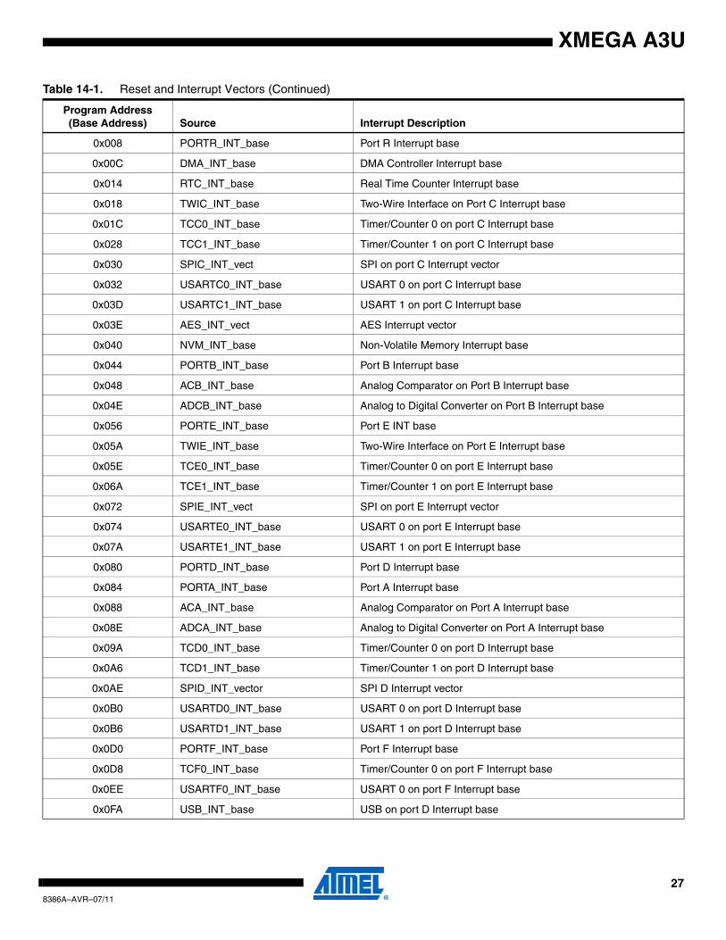
14.3 Interrupt vectors
The interrupt vector is the sum of the peripheral’s base interrupt address and the offset addressfor specific interrupts in each peripheral. The base addresses for the XMEGA A3U devices areshown in Table 14-1. Offset addresses for each interrupt available in the peripheral aredescribed for each peripheral in the XMEGA AU manual. For peripherals or modules that haveonly one interrupt, the interrupt vector is shown in Table 14-1. The program address is the wordaddress.
Table 14-1. Reset and Interrupt Vectors
Program Address(Base Address) Source Interrupt Description
0x000 RESET
0x002 OSCF_INT_vect Crystal Oscillator Failure Interrupt vector (NMI)
0x004 PORTC_INT_base Port C Interrupt base
268386A–AVR–07/11
XMEGA A3U
0x008 PORTR_INT_base Port R Interrupt base
0x00C DMA_INT_base DMA Controller Interrupt base
0x014 RTC_INT_base Real Time Counter Interrupt base
0x018 TWIC_INT_base Two-Wire Interface on Port C Interrupt base
0x01C TCC0_INT_base Timer/Counter 0 on port C Interrupt base
0x028 TCC1_INT_base Timer/Counter 1 on port C Interrupt base
0x030 SPIC_INT_vect SPI on port C Interrupt vector
0x032 USARTC0_INT_base USART 0 on port C Interrupt base
0x03D USARTC1_INT_base USART 1 on port C Interrupt base
0x03E AES_INT_vect AES Interrupt vector
0x040 NVM_INT_base Non-Volatile Memory Interrupt base
0x044 PORTB_INT_base Port B Interrupt base
0x048 ACB_INT_base Analog Comparator on Port B Interrupt base
0x04E ADCB_INT_base Analog to Digital Converter on Port B Interrupt base
0x056 PORTE_INT_base Port E INT base
0x05A TWIE_INT_base Two-Wire Interface on Port E Interrupt base
0x05E TCE0_INT_base Timer/Counter 0 on port E Interrupt base
0x06A TCE1_INT_base Timer/Counter 1 on port E Interrupt base
0x072 SPIE_INT_vect SPI on port E Interrupt vector
0x074 USARTE0_INT_base USART 0 on port E Interrupt base
0x07A USARTE1_INT_base USART 1 on port E Interrupt base
0x080 PORTD_INT_base Port D Interrupt base
0x084 PORTA_INT_base Port A Interrupt base
0x088 ACA_INT_base Analog Comparator on Port A Interrupt base
0x08E ADCA_INT_base Analog to Digital Converter on Port A Interrupt base
0x09A TCD0_INT_base Timer/Counter 0 on port D Interrupt base
0x0A6 TCD1_INT_base Timer/Counter 1 on port D Interrupt base
0x0AE SPID_INT_vector SPI D Interrupt vector
0x0B0 USARTD0_INT_base USART 0 on port D Interrupt base
0x0B6 USARTD1_INT_base USART 1 on port D Interrupt base
0x0D0 PORTF_INT_base Port F Interrupt base
0x0D8 TCF0_INT_base Timer/Counter 0 on port F Interrupt base
0x0EE USARTF0_INT_base USART 0 on port F Interrupt base
0x0FA USB_INT_base USB on port D Interrupt base
Table 14-1. Reset and Interrupt Vectors (Continued)
Program Address(Base Address) Source Interrupt Description
278386A–AVR–07/11
XMEGA A3U
15. I/O Ports
15.1 Features
• General purpose input and output pins with several and individual configuration options• Output driver with configurable driver and pull settings:
– Totem-pole– Wired-AND– Wired-OR– Bus-keeper– Inverted I/O
• Input with synchronous and/or asynchronous sensing with port interrupts and events– Sense both edges– Sense rising edges– Sense falling edges– Sense low level
• Optimal pull-up and pull-down resistor on input and Wired-OR/AND configurations• Optional slew rate control• Asynchronous pin change sensing that can wake-up the device from all sleep modes• Two port interrupts with pin masking per I/O port• Efficient and safe access to port pins
– Hardware read-modify-write through dedicated Toggle/Clear/Set registers– Configuration of multiple pins in a single operation– Mapping of port registers into bit-accessible I/O memory space
• Peripheral Clocks output on port pin• Real Time Counter Clock output to port pin• Event Channel output on port pin• Remap of digital peripheral pin functions
– Selectable USART, SPI and Timer/Counter input/output pin locations
15.2 Overview
One port consists of up to 8 pins ranging from pin 0 to 7. Each port pin can be configured asinput or output with configurable driver and pull settings. They also implement synchronous andasynchronous input sensing with interrupts and events for selectable pin change conditions.Asynchronous pin-change sensing means that a pin change can wake the device from all sleepmodes, included the modes where no clocks are running.
All functions are individual and configurable per pin, but several pins can be configured in onesingle operation. The pins have hardware Read-Modify-Write (RMW) functionality for safe andcorrect change of drive value and/or pull resistor configuration. The direction of one port pin canbe changed without unintentionally changing the direction of any other pin.
The port pin configuration also controls input and output selection of other device function. It ispossible to have both the peripheral clock and the real time clock output to a port pin, and avail-able for external use. The same applies to events from the Event System that can be used tosynchronize and control external functions. Other digital peripherals such as USART, SPI andTimer/Counters can be remapped to selectable pin location in order to optimize pinout versusapplication needs.
288386A–AVR–07/11
XMEGA A3U
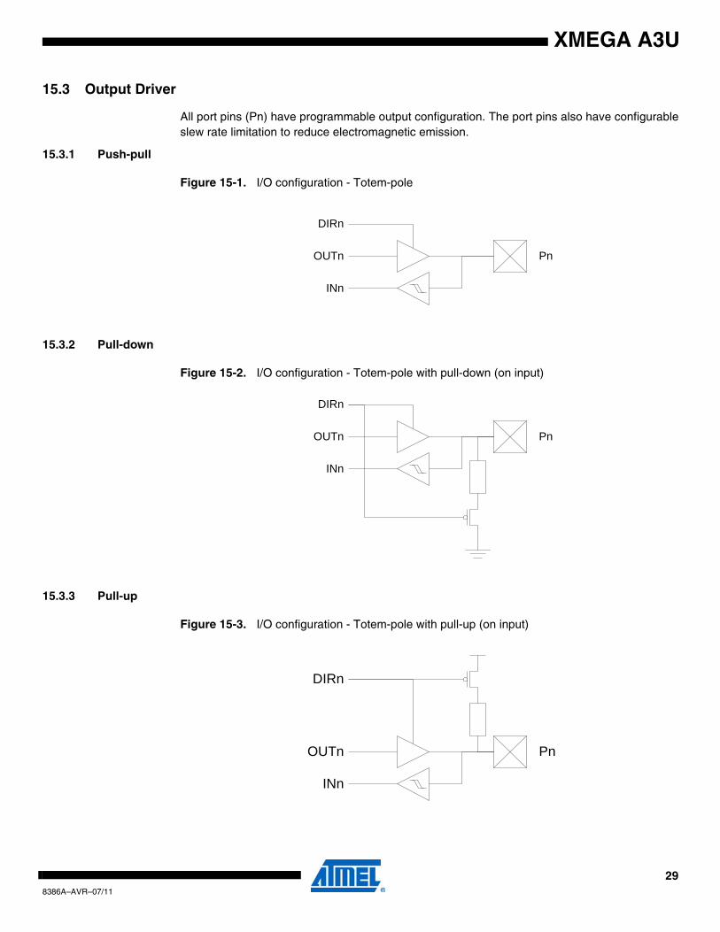
15.3 Output Driver
All port pins (Pn) have programmable output configuration. The port pins also have configurableslew rate limitation to reduce electromagnetic emission.
15.3.1 Push-pull
Figure 15-1. I/O configuration - Totem-pole
15.3.2 Pull-down
Figure 15-2. I/O configuration - Totem-pole with pull-down (on input)
15.3.3 Pull-up
Figure 15-3. I/O configuration - Totem-pole with pull-up (on input)
INn
OUTn
DIRn
Pn
INn
OUTn
DIRn
Pn
INn
OUTn
DIRn
Pn
298386A–AVR–07/11
XMEGA A3U
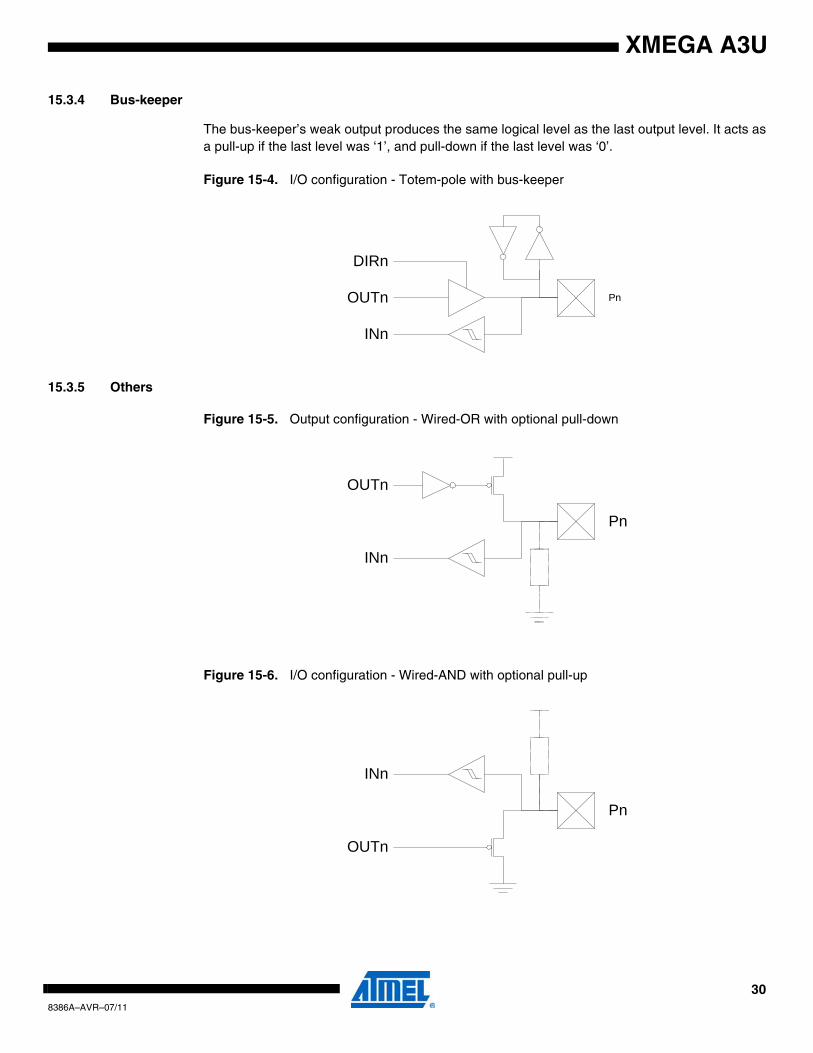
15.3.4 Bus-keeper
The bus-keeper’s weak output produces the same logical level as the last output level. It acts asa pull-up if the last level was ‘1’, and pull-down if the last level was ‘0’.
Figure 15-4. I/O configuration - Totem-pole with bus-keeper
15.3.5 Others
Figure 15-5. Output configuration - Wired-OR with optional pull-down
Figure 15-6. I/O configuration - Wired-AND with optional pull-up
INn
OUTn
DIRn
Pn
INn
OUTn
Pn
INn
OUTn
Pn
308386A–AVR–07/11
XMEGA A3U
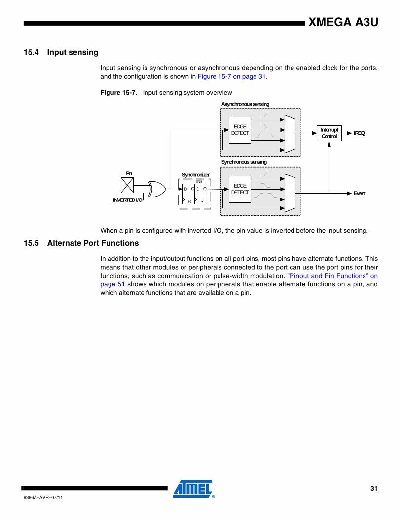
15.4 Input sensing
Input sensing is synchronous or asynchronous depending on the enabled clock for the ports,and the configuration is shown in Figure 15-7 on page 31.
Figure 15-7. Input sensing system overview
When a pin is configured with inverted I/O, the pin value is inverted before the input sensing.
15.5 Alternate Port Functions
In addition to the input/output functions on all port pins, most pins have alternate functions. Thismeans that other modules or peripherals connected to the port can use the port pins for theirfunctions, such as communication or pulse-width modulation. ”Pinout and Pin Functions” onpage 51 shows which modules on peripherals that enable alternate functions on a pin, andwhich alternate functions that are available on a pin.
INVERTED I/O
Interrupt Control IREQ
Event
Pn
D Q
R
D Q
R
SynchronizerINn
EDGE DETECT
Asynchronous sensing
Synchronous sensing
EDGE DETECT
318386A–AVR–07/11
XMEGA A3U
16. T/C - 16-bit Timer/Counter
16.1 Features
• Seven 16-bit Timer/Counters– Four Timer/Counters of type 0– Three Timer/Counters of type 1
• 32-bit Timer/Counter support by cascading two Timer/Counters• Up to 4 Compare or Capture (CC) Channels
– 4 CC Channels for Timer/Counters of type 0– 2 CC Channels for Timer/Counters of type 1
• Double Buffered timer period setting • Double Buffered Capture or Compare Channels• Waveform Generation:
– Frequency Generation– Single Slope Pulse Width Modulation– Dual Slope Pulse Width Modulation
• Input Capture:– Input Capture with noise cancelling– Frequency capture– Pulse width capture– 32-bit input capture
• Timer Overflow and Error interrupts / events• One Compare Match or Input Capture interrupt / event per CC Channel• Can be used with Event System for
– Quadrature Decoding– Count and direction control– Capture
• Can be used with DMA and trigger DMA transactions • High-Resolution Extension
– Increases frequency and waveform resolution by 4x (2-bit), or 8x (3-bit)• Advanced Waveform Extension
– Low and High-side output with programmable Dead-Time Insertion (DTI)• Event controlled fault protection for safe disabling of external drivers
16.2 Overview
There are seven flexible 16-bit Timer/Counters (TC). Their capabilities include accurate programexecution timing, frequency and waveform generation, and input capture with time and fre-quency measurement of digital signals. Two Timer/Counters can be cascaded to create 32-bitTimer/Counter with optional 32-bit capture.
A Timer/Counter consists of a Base Counter and a set of Compare or Capture (CC) channels.The Base Counter can be used to count clock cycles or events. It has direction control andperiod setting that can be used for timing. The CC channels can be used together with the BaseCounter to do compare match control, frequency generation and pulse width waveform modula-tion, or various input capture operations. A Timer/Counter can be configured for either capture orcompare functions, and not perform both at the same time.
328386A–AVR–07/11

XMEGA A3U
A Timer/Counter can be clocked and timed from the Peripheral Clock with optional prescaling orthe Event System. The Event System can also be used for direction control, capture trigger or tosynchronize operations.
Figure 16-1. Overview of a Timer/Counter and closely related peripherals
Figure 16-2. Overview of a Timer/Counter and closely related peripherals
The only difference between Timer/Counter type 0 and 1 is the number of CC Channels.Timer/Counter 0 has four CC channels, and Timer/Counter 1 has two CC channels. All informa-tion related to CC channel 3 and 4 is only valid for Timer/Counter 0.
The High Resolution (Hi-Res) extension can be used to increase the waveform output resolutionby up to eight times, by using internal clock source running up to four times faster than thePeripheral Clock. See ”Hi-Res - High Resolution Extension” on page 35 for more details.
The Advanced Waveform Extension can be enabled to provide extra and more advanced fea-tures for the Timer/Counter. This are only available for Timer/Counter 0. See ”AWeX - AdvancedWaveform Extension” on page 34 for more details.
PORTC, PORTD and PORTE each has one Timer/Counter 0 and one Timer/Counter1. PORTFhas one Timer/Counter 0. Notation of these are TCC0 (Time/Counter C0), TCC1, TCD0, TCD1,TCE0, TCE1 and TCF0, respectively.
AWeX
Compare/Capture Channel DCompare/Capture Channel C
Compare/Capture Channel BCompare/Capture Channel A
Waveform GenerationBuffer
Comparator Hi-R
es
Fault Protection
Capture Control
Base Counter
CounterControl Logic
Timer PeriodPrescaler
Dead-Time Insertion
Pattern Generation
clkPER4
POR
T
Event System
clkPER
Timer/Counter
338386A–AVR–07/11
XMEGA A3U
17. AWeX - Advanced Waveform Extension
17.1 Features
• Wafeform output with complementary output from each Compare channel• 4 Dead-Time Insertion (DTI) Units
– 8-bit Resolution– Separate High and Low Side Dead-Time Setting– Double Buffered Dead-Time– Optionally halts Timer during Dead-Time Insertion
• Pattern Generation unit creating synchronised bit pattern across the port pins– Double buffered pattern generation– Optionally distribution of one Compare channel output across the port pins
• Event controlled Fault Protection for instant and predictably fault triggering
17.2 Overview
The Advanced Waveform Extension (AWeX) provides extra functions to the Timer/Counter inWaveform Generation (WG) modes. It is primarily intended for different types of motor controland other power control applications. It enables Low- and High Side output with Dead TimeInsertion, and fault protection for disabling and shutdown of drivers. It can also generate a syn-chronized bit pattern across the port pins.
Each of the waveform generator outputs from the Timer/Counter 0 are split into a complimentarypair of outputs when any AWeX features are enabled. These output pairs go through a Dead-Time Insertion (DTI) unit that generates the non-inverted Low Side (LS) and inverted High Side(HS) of the WG output with dead time insertion between LS and HS switching. The DTI outputwill override the normal port value according to the port override setting.
The Pattern Generation unit can be used to generate a synchronized bit pattern across the portit is connected to. In addition, the WG output from the Compare Channel A can be distributed toand override all the port pins. When the Pattern Generator unit is enabled the DTI unit isbypassed.
The Fault Protection unit is connected to the Event System, enabling any event to trigger a faultcondition that will disable the AWeX output. The Event System ensure predictable and instantfault reaction, and gives great flexibility in the selection of fault triggers.
The AWEX is available for TCC0. The notation of this is AWEXC.
348386A–AVR–07/11
XMEGA A3U
18. Hi-Res - High Resolution Extension
18.1 Features• Increases Waveform Generator resolution by up to 8 times (3-bit)• Supports Frequency, Single Slope PWM and Dual Slope PWM generation• Supports the AWEX when this is used for the same Timer/Counter
18.2 OverviewThe Hi-Resolution (Hi-Res) Extension is able to increase the resolution of the waveform genera-tion output by a factor of four or eight. It can be used for a Timer/Counter doing Frequency,Single Slope PWM or Dual Slope PWM generation. It can also be used with the AWeX if this isused for the same Timer/Counter.
Atmel® AVR® XMEGA® A3U devices have four Hi-Res Extensions that each can be enabled foreach Timer/Counters pair on PORTC, PORTD, PORTE and PORTF. The notation of these areHIRESC, HIRESD, HIRESE and HIRESF, respectively.
358386A–AVR–07/11
XMEGA A3U
19. RTC - 16-bit Real-Time Counter
19.1 Features
• 16-bit resolution• Selectable clock source
– 32.768kHz external crystal– External clock– 32.768kHz internal oscillator– 32kHz internal ULP oscillator
• Programmable 10-bit clock prescaling• One Compare register• One Period register• Clear Counter on period overflow • Optional Interrupt/ Event on overflow and compare match
19.2 Overview
The 16-bit Real Time Counter (RTC) is a counter that typically runs continuously, including inlow power sleep modes, to keep track of time. It can wake up the device from sleep modesand/or interrupt the device at regular intervals.
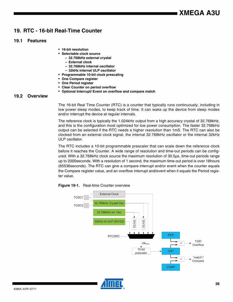
The reference clock is typically the 1.024kHz output from a high accuracy crystal of 32.768kHz,and this is the configuration most optimized for low power consumption. The faster 32.768kHzoutput can be selected if the RTC needs a higher resolution than 1mS. The RTC can also beclocked from an external clock signal, the internal 32.768kHz oscillator or the internal 32kHzULP oscillator.
The RTC includes a 10-bit programmable prescaler that can scale down the reference clockbefore it reaches the Counter. A wide range of resolution and time-out periods can be config-ured. With a 32.768kHz clock source the maximum resolution of 30.5µs, time-out periods rangeup to 2000seconds. With a resolution of 1 second, the maximum time-out period is over 18hours(65536seconds). The RTC can give a compare interrupt and/or event when the counter equalsthe Compare register value, and an overflow interrupt and/event when it equals the Period regis-ter value.
Figure 19-1. Real-time Counter overview
32.768kHz Crystal Osc
32.768kHz Int. Osc
TOSC1
TOSC2
External Clock
DIV
32
DIV
32
32kHz int ULP (DIV32)
RTCSRC
10-bitprescaler
clkRTC
CNT
PER
COMP
=
=
”match”/Compare
TOP/Overflow
368386A–AVR–07/11
XMEGA A3U
20. USB - Universal Serial Bus Interface
20.1 Features
• One USB 2.0 full speed (12Mbps) and low speed (1.5Mbps) device compliant interface• Integrated on-chip USB transceiver, no external components needed• 16 endpoint addresses with full endpoint flexibility for up to 32 endpoints
– One input endpoint per endpoint address– One output endpoint per endpoint address
• Endpoint address transfer type selectable to– Control transfers– Interrupt transfers– Bulk transfers– Isochronous transfers
• Configurable data payload size per endpoint, up to 1023bytes• Endpoint configuration and data buffers located in internal SRAM
– Configurable location for endpoint configuration data– Configurable location for each endpoint's data buffer
• Built in Direct Memory Access (DMA) to internal SRAM for– Endpoint configurations– Read and write of endpoint data
• Ping-Pong operation for higher throughput and double buffered operation– Input and output endpoint data buffers used in a single direction– CPU/DMA controller can update data buffer during transfer
• Multi-Packet transfer for reduced interrupt load and software intervention– Data payload exceeding max packet size is transferred in one continuous transfer– No interrupts or software interaction on packet transaction level
• Transaction Complete FIFO for easy flow management when using multiple endpoints– Tracks all completed transactions in a first come, first serve work-queue
• Clock selection independent of System Clock source selection• Connection to Event System• On chip debug possibilities during USB transactions
20.2 Overview
The USB interface is an USB 2.0 full speed (12Mbps) and low speed (1.5Mbps) device compli-ant interface.
It supports 16 endpoint addresses. All endpoint addresses have one input and one output end-point, for a total of 32 endpoints. Each endpoint address is fully configurable and can beconfigured for any of the four transfer types: control, interrupt, bulk or isochronous. The datapayload size is also selectable and it supports data payloads up to 1023bytes.
No dedicated memory is allocated for or included in the USB module. Internal SRAM is used tokeep the configuration for each endpoint address, and the data buffer for each endpoint. Thememory locations used for endpoint configurations and data buffers are fully configurable. Theamount of memory allocated is fully dynamic according to the number of endpoints in use, andthe configuration of these. The USB module has built-in Direct Memory Access (DMA) and willread/write data from/to the SRAM when a USB transaction takes place.
To maximise throughput, an endpoint address can be configured for Ping-Pong operation. Whenthis is done, the input and output endpoints are both used in the same direction. The CPU or
378386A–AVR–07/11
XMEGA A3U
DMA Controller can then read/write one data buffer while the USB module writes/reads theother, and vice versa. This gives double buffered communication.
Multi-packet transfer enables a data payload exceeding the maximum packet size of an end-pointto be transferred as multiple packets without software intervention. This reduce the CPUintervention and the interrupts needed for USB transfers.
For low power operation, the USB module can put the microcontroller in any sleep mode whenthe USB bus is idle and a suspend condition is given. Upon bus resume, the USB module canwake the microcontroller from any sleep mode.
PORTD has one USB. Notation of this is USBD.
388386A–AVR–07/11
XMEGA A3U
21. TWI - Two Wire Interface
21.1 Features
• Two Identical Two Wire Interface peripherals• Bi-directional two-wire communication interface
– Phillips I2C compatible– System Management Bus (SMBus) compatible
• Bus master and slave operation supported– Slave operation– Single bus master operation– Bus master in multi-master bus environment– Multi-master arbitration
• Flexible slave address match functions– 7-bit and General Call Address Recognition in Hardware– 10-bit addressing supported– Address mask register for dual address match or address range masking– Optional software address recognition for unlimited number of addresses
• Slave can operate in all sleep modes• Slave address match can wake device from all sleep modes• 100kHz and 400kHz bus frequency support • Slew-rate limited output drivers• Input filter for bus noise and spike suppression• Support arbitration between START/Repeated START and Data Bit (SMBus)• Slave arbitration allows support for Address Resolve Protocol (ARP) (SMBus)
21.2 Overview
The Two Wire Interface is a bi-directional two-wire communication interface. It is I2C and SystemManagement Bus (SMBus) compatible. The only external hardware needed to implement thebus is one pull-up resistor on each bus line.
The TWI module supports master and slave functionality. The master and slave functionality areseparated from each other and can be enabled and configured separately. The master modulesupports multi-master bus operation and arbitration. It contains the baud rate generator. Both100kHz and 400kHz bus frequency is supported.
The slave module implements 7-bit address match and general address call recognition in hard-ware. 10-bit addressing is also supported. A dedicated address mask register can act as asecond address match register or as a register for address range masking. The slave continuesto operate in all sleep modes, including Power down mode. This enables the slave to wake upthe device from all sleep modes on TWI address match. It is possible to disable the addressmatching to let this be handled in software instead. Smart Mode can be enabled to auto triggeroperations and reduce software complexity.
The TWI module will detect START and STOP conditions, bus collision and bus errors. Arbitra-tion lost, errors, collision and clock hold on the bus is also detected and indicated in separatestatus flags available in both master and slave mode.
It is possible to disable the TWI drivers in the device, and enable a 4-wire digital interface forconnecting to an external TWI bus driver. This can be used for applications where the deviceoperates from a different VCC voltage than used by the TWI bus.
PORTC and PORTE each has one TWI. Notation of these peripherals are TWIC and TWIE.
398386A–AVR–07/11
XMEGA A3U
22. SPI - Serial Peripheral Interface
22.1 Features
• Three Identical SPI peripherals• Full-duplex, Three-wire Synchronous Data Transfer• Master or Slave Operation• LSB First or MSB First Data Transfer• Seven Programmable Bit Rates• Interrupt Flag at the End of Transmission• Write collision flag to indicate data collision• Wake-up from Idle Mode• Double Speed Master Mode
22.2 Overview
The Serial Peripheral Interface (SPI) is a high-speed synchronous data transfer interface usingthree or four pins. It allows fast communication between an XMEGA device and peripheraldevices or other microcontrollers. The SPI supports full duplex communication.
A device connected to the bus must act as a master or slave. The master initiates and controlsall data transactions, and data is transferred both to and from the device simultaneously.
PORTC, PORTD, and PORTE each has one SPI. Notation of these peripherals are SPIC, SPID,and SPIE respectively.
408386A–AVR–07/11
XMEGA A3U
23. USART
23.1 Features
• Seven Identical USART peripherals• Full Duplex Operation• Asynchronous or Synchronous Operation
– Synchronous clock rates up to 1/2 o the device clock frequency– Asynchronous clock rates up to 1/8 of the device clock frequency
• Supports Serial Frames with 5, 6, 7, 8, or 9 Data Bits and 1 or 2 Stop Bits• Fractional Baud Rate Generator
– Can generate desired baud rate from any system clock frequency– No need for external oscillator with certain frequencies
• Built in error detection and correction schemes – Odd or Even Parity Generation and Parity Check – Data Over Run and Framing Error Detection– Noise Filtering Includes False Start Bit Detection and Digital Low Pass Filter
• Separate Interrupts for– Transmit Complete– Transmit Data Register Empty– Receive Complete
• Multi-Processor Communication Mode– Addressing scheme to address a specific devices on a multi-device bus– Enable unaddressed devices to automatically ignore all frames
• Master SPI Mode– Double Buffered Operation– Configurable Data Order– High Speed Operation up to 1/2 of the peripheral clock frequency
• IRCOM Module for IrDA compliant pulse modulation/demodulation23.2 Overview
The Universal Synchronous and Asynchronous serial Receiver and Transmitter (USART) is afast and flexible serial communication module. The USART supports full duplex communication,and both asynchronous and clocked synchronous operation. The USART can also be set inMaster SPI mode and be used for SPI communication.
Communication is frame based, and the frame format can be customized to support a widerange of standards. The USART is buffered in both direction, enabling continued data transmis-sion without any delay between frames. There are separate interrupts for receive and transmitcomplete, enabling fully interrupt driven communication. Frame error and buffer overflow aredetected in hardware and indicated with separate status flags. Even or odd parity generationand parity check can also be enabled.
The Clock Generation logic has a fractional baud rate generator that is able to generate a widerange of USART baud rates from any system clock frequencies. This remove the need to usean external crystal oscillator with a certain frequency in order to achieve a required baud rate. Italso includes support external clock input in synchronous slave operation.
One USART can use the IRCOM module to support IrDA 1.4 physical compliant pulse modula-tion and demodulation for baud rates up to 115.2kbps.
PORTC, PORTD, and PORTE each has two USARTs, while PORTF has one USART only.Notation of these peripherals are USARTC0, USARTC1, USARTD0, USARTD1, USARTE0,USARTE1 and USARTF0, respectively.
418386A–AVR–07/11
XMEGA A3U
24. IRCOM - IR Communication Module
24.1 Features
• Pulse modulation/demodulation for infrared communication• IrDA Compatible for baud rates up to 115.2kbps• Selectable pulse modulation scheme
– 3/16 of baud rate period– Fixed pulse period, 8-bit programmable– Pulse modulation disabled
• Built in filtering• Can be connected to and used by one USART at a time
24.2 Overview
The Infrared Communication Module (IRCOM) is used for IrDA communication with baud ratesup to 115.2kbps. There is one IRCOM available which can be connected to any USART toenable infrared pulse coding/decoding for that USART.
428386A–AVR–07/11
XMEGA A3U
25. AES and DES Crypto Engine
25.1 Features
• Data Encryption Standard (DES) CPU instruction• Advanced Encryption Standard (AES) Crypto module• DES Instruction
– Encryption and Decryption– Single-cycle DES instruction– Encryption/Decryption in 16 clock cycles per 8-byte block
• AES Crypto Module– Encryption and Decryption– Support 128-bit keys– Support XOR data load mode to the State memory for Cipher Block Chaining– Encryption/Decryption in 375 clock cycles per 16-byte block
25.2 Overview
The Advanced Encryption Standard (AES) and Data Encryption Standard (DES) are two com-monly used standards for cryptography. These are supported through an AES peripheralmodule and a DES CPU instruction, and the communication interfaces and the CPU can usethese for fast encrypted communication and secure data storage.
DES is supported by an instruction in the AVR CPU. The 8-byte key and 8-byte data blocks mustbe loaded into the Register file, and then the DES instruction must be executed 16 times toencrypt/decrypt the data block.
The AES Crypto Module encrypts and decrypts 128-bit data blocks with the use of a 128-bit key.The key and data must be loaded into the key and state memory in the module before encryp-tion/ decryption is started. It takes 375 Peripheral clock cycles before the encryption/decryptionis done. The encrypted/encrypted data can then be read out, and an optional interrupt can begenerated. The AES Crypto Module also has DMA support with transfer triggers when encryp-tion/decryption is done and optional auto-start of encryption/decryption when the state memoryis fully loaded.
438386A–AVR–07/11
XMEGA A3U
26. CRC - Cyclic Redundancy Check Generator
26.1 Features• Cyclic Redundancy Check (CRC) Generation and Checking for
– Communication Data– Program or Data in Flash memory– Data in SRAM memory and I/O memory space
• Integrated with Flash memory, DMA Controller and CPU– Continuous CRC on data going through a DMA Channel– Automatic CRC of the complete, or selectable range of the Flash memory– CPU can load data to CRC Generator through I/O interface
• CRC polynomial software selectable to– CRC-16 (CRC-CCITT)– CRC-32 (IEEE 802.3)
• Zero remainder detection
26.2 OverviewA Cyclic Redundancy Check (CRC) is a test algorithm used to detect accidental errors on data,and is commonly used to determine the correctness of a data transmission, data memory andprogram memory. A CRC takes a data stream or block of data as input and generates a 16- or32-bit output that can be kept with the data and used as checksum. When the same data is laterreceived or read, the device or application repeats the calculation. If the new CRC calculationdoes not match the one calculated earlier, the block contains a data error. The application willthen detect this and may take corrective action such as requesting the data to be sent again.
Typically, an n-bit CRC, applied to a data block of arbitrary length, will detect any single errorburst not longer than n bits (in other words, any single alteration that spans no more than n bitsof the data), and will detect a fraction 1-2-n of all longer error bursts.The CRC module in XMEGAsupports two commonly used CRC polynomials; CRC-16 (CRC-CCITT) and CRC-32 (IEEE802.3).
• CRC-16:
• CRC-32:
Polynomial: x16+x12+x5+1
Hex value: 0x1021
Polynomial: x32+x26+x23+x22+x16+x12+x11+x10+x8+x7+x5+x4+x2+x+1
Hex value: 0x04C11DB7
448386A–AVR–07/11
XMEGA A3U
27. ADC - 12-bit Analog to Digital Converter
27.1 Features
• Two Analog to Digital Converters• 12-bit resolution• Up to 2 Million Samples Per Second
– 4 inputs can be sampled within 1.5µs– Down to 2.5µs conversion time with 8-bit resolution– Down to 3.5µs conversion time with 12-bit resolution
• Differential and Single-ended input– Up to 16 single-ended inputs– 16x4 differential inputs without gain– 16x4 differential input with gain
• Built in differential gain stage– 1/2x, 1x, 2x, 4x, 8x, 16x, 32x and 64x gain options
• Single, continues and scan conversion options• 4 internal inputs
– Internal Temperature sensor– DAC Output– VCC voltage divided by 10– 1.1V Bandgap voltage
• 4 conversion channels with individual input control and result registers– Enable 4 parallel configurations and results
• Internal and external reference options• Compare function for accurate monitoring of user defined thresholds• Optional event triggered conversion for accurate timing• Optional DMA transfer of conversion results• Optional interrupt/event on compare result
27.2 Overview
There are two Analog to Digital Converters (ADCs) modules that can be operated simultane-ously, individually or synchronized.
The ADC converts analog signals to digital values. The ADC has 12-bit resolution and is capableof converting up to 2Million Samples Per Second (MSPS). The input selection is flexible, andboth single-ended and differential measurements can be done. For differential measurementsan optional gain stage is available to increase the dynamic range. In addition several internalsignal inputs are available. The ADC can provide both signed and unsigned results.
This is a pipelined ADC that consists of several consecutive stages. The pipelined design allowshigh sample rate at a low System Clock frequency. It also means that a new input can be sam-pled and a new ADC conversion started while other ADC conversions are still ongoing. Thisremove dependencies between sample rate and propagation delay.
The ADC has four conversion channels (Channel 0-3) with individual input selection, result reg-isters and conversion start control. The ADC can then keep and use four parallel configurationsand results, and this will ease use for applications with high data throughput or multiple modulesusing the ADC independently. It is possible to use DMA to move ADC results directly to memoryor peripherals when conversions are done.
Both internal and external reference voltages can be used. An integrated temperature sensor isavailable for use with the ADC. The output from the DAC, VCC/10 and the Bandgap voltage canalso be measured by the ADC.
458386A–AVR–07/11
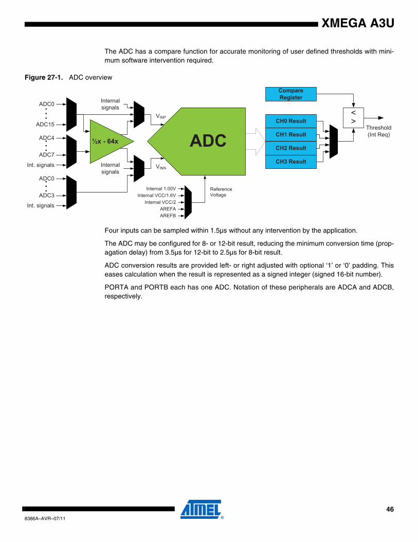
XMEGA A3U
The ADC has a compare function for accurate monitoring of user defined thresholds with mini-mum software intervention required.
Figure 27-1. ADC overview
Four inputs can be sampled within 1.5µs without any intervention by the application.
The ADC may be configured for 8- or 12-bit result, reducing the minimum conversion time (prop-agation delay) from 3.5µs for 12-bit to 2.5µs for 8-bit result.
ADC conversion results are provided left- or right adjusted with optional ‘1’ or ‘0’ padding. Thiseases calculation when the result is represented as a signed integer (signed 16-bit number).
PORTA and PORTB each has one ADC. Notation of these peripherals are ADCA and ADCB,respectively.
ADC CH1 Result
CH0 Result
CH2 Result
Compare Register
<>
½x - 64x
Threshold(Int Req)
Internal 1.00VInternal VCC/1.6V
AREFAAREFB
VINP
VINN
Internalsignals
Internal VCC/2
Internalsignals
CH3 Result
ADC0
ADC15
ADC4
ADC7
•••
•••
ADC0
ADC3
•••
Int. signals
Int. signals
Reference Voltage
468386A–AVR–07/11
XMEGA A3U
28. DAC - 12-bit Digital to Analog Converter
28.1 Features
• One Digital to Analog Converter (DAC)• 12-bit resolution• Up to 1Million Samples Per Second conversion rate per DAC channel• Built in calibration that removes
– Offset error– Gain error
• Multiple conversion trigger sources– On new available data– Events from the Event System
• High drive capabilities and support for– Resistive load– Capacitive load– Combined resistive and capacitive load
• Internal and external reference options• DAC output available as input to Analog Comparator and ADC• Low Power mode with reduced drive strength• Optional DMA transfer of data
28.2 Overview
The Digital to Analog Converter (DAC) converts digital values to voltages. Each DAC has twochannels, 12-bit resolution, and is capable of converting 1Million Samples Per Second (MSPS)on each channels. The built-in calibration system can remove offset and gain error when loadedwith calibration values from software.
Figure 28-1. DAC overview
A DAC conversion is automatically started when new data to be converted is available. Eventfrom the Event System can also be used, and this enable synchronized and timed conversionsbetween the DAC and other peripherals such as a Timer/Counter. The DMA Controller can beused to transfer data to the DAC.
The DAC has high drive strengths and is capable of driving both resistive and capacitive loads,and a load which is a combination of this. A low power mode is available, and this will reduce thedrive strengths of the output. Both internal and external voltage reference can be used. TheDAC output is also internally available for use as input to the Analog Comparator or ADC.
PORTB each has one DAC. Notation of this peripheral is DACB.
DAC0
DAC1
CTRLA
CH1DATA
CH0DATA
Trigger
Trigger
Internal Output enable
Enable
Internal 1.00VAREFAAREFB
Referenceselection
AVCC
Output Driver
Output Driver
DATA
Int.driver
DATA
CTRLB
DMA req(Data Empty)
DMA req(Data Empty)
Select
12
12
Select
Enable
ToAC/ADC
478386A–AVR–07/11
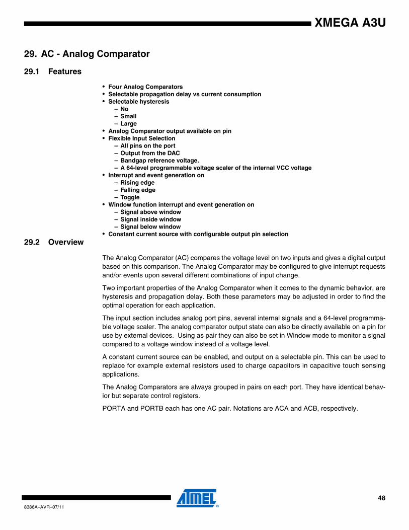
XMEGA A3U
29. AC - Analog Comparator
29.1 Features
• Four Analog Comparators• Selectable propagation delay vs current consumption• Selectable hysteresis
– No– Small– Large
• Analog Comparator output available on pin• Flexible Input Selection
– All pins on the port– Output from the DAC– Bandgap reference voltage.– A 64-level programmable voltage scaler of the internal VCC voltage
• Interrupt and event generation on– Rising edge– Falling edge– Toggle
• Window function interrupt and event generation on– Signal above window– Signal inside window– Signal below window
• Constant current source with configurable output pin selection29.2 Overview
The Analog Comparator (AC) compares the voltage level on two inputs and gives a digital outputbased on this comparison. The Analog Comparator may be configured to give interrupt requestsand/or events upon several different combinations of input change.
Two important properties of the Analog Comparator when it comes to the dynamic behavior, arehysteresis and propagation delay. Both these parameters may be adjusted in order to find theoptimal operation for each application.
The input section includes analog port pins, several internal signals and a 64-level programma-ble voltage scaler. The analog comparator output state can also be directly available on a pin foruse by external devices. Using as pair they can also be set in Window mode to monitor a signalcompared to a voltage window instead of a voltage level.
A constant current source can be enabled, and output on a selectable pin. This can be used toreplace for example external resistors used to charge capacitors in capacitive touch sensingapplications.
The Analog Comparators are always grouped in pairs on each port. They have identical behav-ior but separate control registers.
PORTA and PORTB each has one AC pair. Notations are ACA and ACB, respectively.
488386A–AVR–07/11
XMEGA A3U
Figure 29-1. Analog comparator overview
The window function is realized by connecting the external inputs of the two analog comparatorsin a pair as shown in Figure 29-2..
Figure 29-2. Analog comparator window function
Voltage Scaler ACnMUXCTRL ACnCTRL
Interrupt Mode
Enable
Enable
Hysteresis
Hysteresis
DAC
Bandgap
AC1OUT
WINCTRL
InterruptSensititivity
Control&
WindowFunction
Events
Interrupts
AC0OUT
Pin Input
Pin Input
Pin Input
Pin Input
AC0
+
-
AC1
+
-
Input signal
Upper limit of window
Lower limit of window
Interrupt sensitivity
control
Interrupts
Events
498386A–AVR–07/11
XMEGA A3U
30. Programming and Debugging
30.1 Features
• Programming– External programming through the PDI or JTAG interface
Minimal protocol overhead for fast operationBuilt in error detection and handling for reliable operation
– Bootloader support for programming through any communication interface• Debugging
– Non-Intrusive Real-Time On-Chip Debug System– No software or hardware resources required from device expect pin connection– Program Flow Control
Go, Stop, Reset, Step into, Step over, Step out, Run-to-Cursor– Unlimited Number of User Program Breakpoints– Unlimited Number of User Data Breakpoints, break on:
Data location read, write or both read and writeData location content equal or not equal to a valueData location content is greater or smaller than a valueData location content is within or outside a range
– No limitation on device clock frequency• Program and Debug Interface (PDI)
– 2-pin interface for external programming and debugging– Uses the Reset pin and a dedicated pin– No I/O pins required during programming or debugging
• JTAG Interface– 4-pin IEEE std. 1149.1 compliant interface for programming and debugging– Boundary-scan capabilities According to the IEEE std. 1149.1 (JTAG) Standard
30.2 Overview
Atmel® AVR® XMEGA® devices together with Atmel’s development tool chain include the neces-sary functions for efficient development. All external programming and debugging are donethrough the Program and Debug Interface (PDI), or the JTAG interface.
The Program and Debug Interface is 2-pin interface that uses the Reset pin and a dedicated pin.No I/O pins are required during programming or debugging.
The JTAG Interface is a 4-pin IEEE std. 1149.1 compliant interface. This also has Boundary-scan capabilities according to the IEEE std. 1149.1 (JTAG) Standard
In addition to the PDI and JTAG interface, programming can also be done through a bootloader.A bootloader in the device can use any other communication interface such as UART, TWI orSPI to download and program new application code to the Flash memory.
Debug is supported through a on-chip debug system that offers Non-Intrusive Real-Time debug.It does not require any software or hardware resources expect for the device expect pin connec-tion. Using Atmel’s tool chain, it offers complete program flow control and has supported forunlimited number of program and complex data breakpoints. Application debug can be donefrom C and high level language source code level, as well as assembler and disassembler level.
508386A–AVR–07/11
XMEGA A3U
31. Pinout and Pin Functions
The device pinout is shown in ”Pinout/Block Diagram” on page 3. In addition to general purposeI/O functionality, each pin can have several alternate functions. This will depend on whichperipheral is enabled and connected to the actual pin. Only one of the pin functions can be usedat time.
31.1 Alternate Pin Function DescriptionThe tables below show the notation for all pin functions available and describe its function.
31.1.1 Operation/Power Supply
31.1.2 Port Interrupt functions
31.1.3 Analog functions
31.1.4 Timer/Counter and AWEX functions
VCC Digital supply voltage
AVCC Analog supply voltage
GND Ground
SYNC Port pin with full synchronous and limited asynchronous interrupt function
ASYNC Port pin with full synchronous and full asynchronous interrupt function
ACn Analog Comparator input pin n
ACnOUT Analog Comparator n Output
ADCn Analog to Digital Converter input pin n
DACn Digital to Analog Converter output pin n
AREF Analog Reference input pin
OCnxLS Output Compare Channel x Low Side for Timer/Counter n
OCnxHS Output Compare Channel x High Side for Timer/Counter n
518386A–AVR–07/11
XMEGA A3U
31.1.5 Communication functions
31.1.6 Oscillators, Clock and Event
31.1.7 Debug/System functions
SCL Serial Clock for TWI
SDA Serial Data for TWI
SCLIN Serial Clock In for TWI when external driver interface is enabled
SCLOUT Serial Clock Out for TWI when external driver interface is enabled
SDAIN Serial Data In for TWI when external driver interface is enabled
SDAOUT Serial Data Out for TWI when external driver interface is enabled
XCKn Transfer Clock for USART n
RXDn Receiver Data for USART n
TXDn Transmitter Data for USART n
SS Slave Select for SPI
MOSI Master Out Slave In for SPI
MISO Master In Slave Out for SPI
SCK Serial Clock for SPI
D- Data- for USB
D+ Data+ for USB
TOSCn Timer Oscillator pin n
XTALn Input/Output for Oscillator pin n
CLKOUT Peripheral Clock Output
EVOUT Event Channel 0 Output
RTCOUT RTC Clock Source Output
RESET Reset pin
PDI_CLK Program and Debug Interface Clock pin
PDI_DATA Program and Debug Interface Data pin
TCK JTAG Test Clock
TDI JTAG Test Data In
TDO JTAG Test Data Out
TMS JTAG Test Mode Select
528386A–AVR–07/11
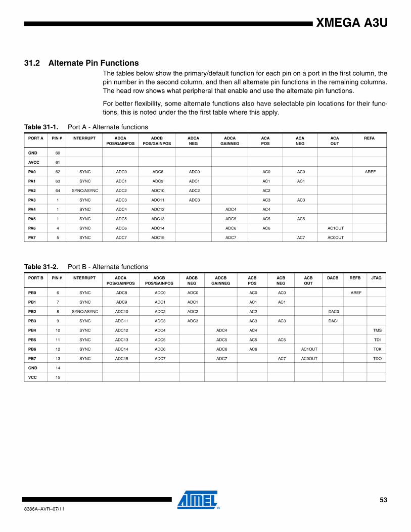
XMEGA A3U
31.2 Alternate Pin FunctionsThe tables below show the primary/default function for each pin on a port in the first column, thepin number in the second column, and then all alternate pin functions in the remaining columns.The head row shows what peripheral that enable and use the alternate pin functions.
For better flexibility, some alternate functions also have selectable pin locations for their func-tions, this is noted under the the first table where this apply.
Table 31-1. Port A - Alternate functions
PORT A PIN # INTERRUPT ADCAPOS/GAINPOS
ADCBPOS/GAINPOS
ADCANEG
ADCAGAINNEG
ACAPOS
ACANEG
ACAOUT
REFA
GND 60
AVCC 61
PA0 62 SYNC ADC0 ADC8 ADC0 AC0 AC0 AREF
PA1 63 SYNC ADC1 ADC9 ADC1 AC1 AC1
PA2 64 SYNC/ASYNC ADC2 ADC10 ADC2 AC2
PA3 1 SYNC ADC3 ADC11 ADC3 AC3 AC3
PA4 1 SYNC ADC4 ADC12 ADC4 AC4
PA5 1 SYNC ADC5 ADC13 ADC5 AC5 AC5
PA6 4 SYNC ADC6 ADC14 ADC6 AC6 AC1OUT
PA7 5 SYNC ADC7 ADC15 ADC7 AC7 AC0OUT
Table 31-2. Port B - Alternate functions
PORT B PIN # INTERRUPT ADCAPOS/GAINPOS
ADCBPOS/GAINPOS
ADCBNEG
ADCBGAINNEG
ACBPOS
ACBNEG
ACBOUT
DACB REFB JTAG
PB0 6 SYNC ADC8 ADC0 ADC0 AC0 AC0 AREF
PB1 7 SYNC ADC9 ADC1 ADC1 AC1 AC1
PB2 8 SYNC/ASYNC ADC10 ADC2 ADC2 AC2 DAC0
PB3 9 SYNC ADC11 ADC3 ADC3 AC3 AC3 DAC1
PB4 10 SYNC ADC12 ADC4 ADC4 AC4 TMS
PB5 11 SYNC ADC13 ADC5 ADC5 AC5 AC5 TDI
PB6 12 SYNC ADC14 ADC6 ADC6 AC6 AC1OUT TCK
PB7 13 SYNC ADC15 ADC7 ADC7 AC7 AC0OUT TDO
GND 14
VCC 15
538386A–AVR–07/11
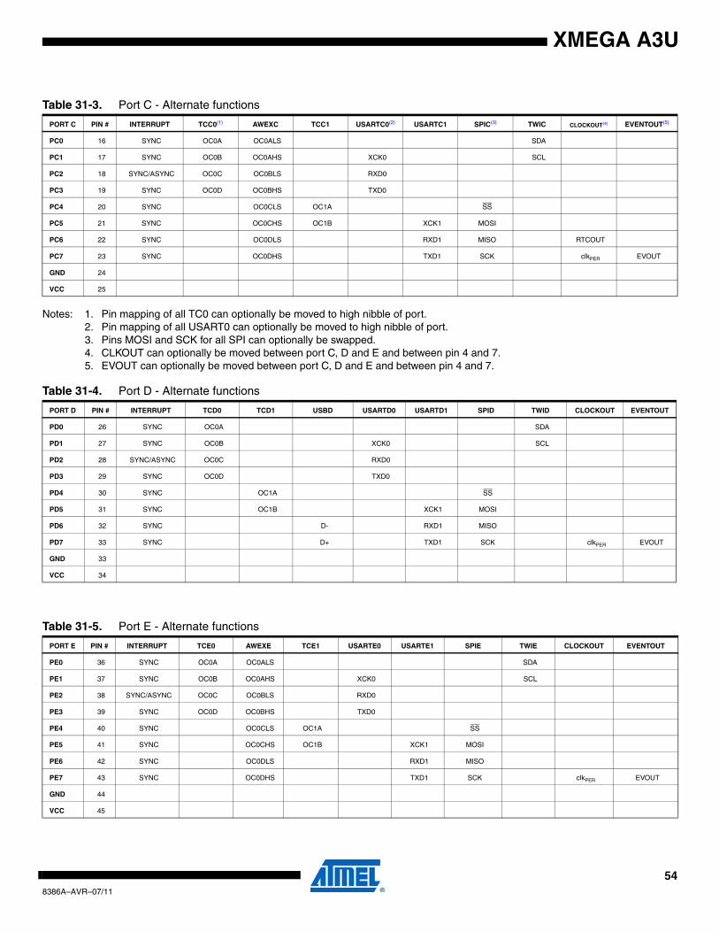
XMEGA A3U
Notes: 1. Pin mapping of all TC0 can optionally be moved to high nibble of port.2. Pin mapping of all USART0 can optionally be moved to high nibble of port.3. Pins MOSI and SCK for all SPI can optionally be swapped.4. CLKOUT can optionally be moved between port C, D and E and between pin 4 and 7.5. EVOUT can optionally be moved between port C, D and E and between pin 4 and 7.
Table 31-3. Port C - Alternate functions
PORT C PIN # INTERRUPT TCC0(1) AWEXC TCC1 USARTC0(2) USARTC1 SPIC(3) TWIC CLOCKOUT(4) EVENTOUT(5)
PC0 16 SYNC OC0A OC0ALS SDA
PC1 17 SYNC OC0B OC0AHS XCK0 SCL
PC2 18 SYNC/ASYNC OC0C OC0BLS RXD0
PC3 19 SYNC OC0D OC0BHS TXD0
PC4 20 SYNC OC0CLS OC1A SS
PC5 21 SYNC OC0CHS OC1B XCK1 MOSI
PC6 22 SYNC OC0DLS RXD1 MISO RTCOUT
PC7 23 SYNC OC0DHS TXD1 SCK clkPER EVOUT
GND 24
VCC 25
Table 31-4. Port D - Alternate functions
PORT D PIN # INTERRUPT TCD0 TCD1 USBD USARTD0 USARTD1 SPID TWID CLOCKOUT EVENTOUT
PD0 26 SYNC OC0A SDA
PD1 27 SYNC OC0B XCK0 SCL
PD2 28 SYNC/ASYNC OC0C RXD0
PD3 29 SYNC OC0D TXD0
PD4 30 SYNC OC1A SS
PD5 31 SYNC OC1B XCK1 MOSI
PD6 32 SYNC D- RXD1 MISO
PD7 33 SYNC D+ TXD1 SCK clkPER EVOUT
GND 33
VCC 34
Table 31-5. Port E - Alternate functions
PORT E PIN # INTERRUPT TCE0 AWEXE TCE1 USARTE0 USARTE1 SPIE TWIE CLOCKOUT EVENTOUT
PE0 36 SYNC OC0A OC0ALS SDA
PE1 37 SYNC OC0B OC0AHS XCK0 SCL
PE2 38 SYNC/ASYNC OC0C OC0BLS RXD0
PE3 39 SYNC OC0D OC0BHS TXD0
PE4 40 SYNC OC0CLS OC1A SS
PE5 41 SYNC OC0CHS OC1B XCK1 MOSI
PE6 42 SYNC OC0DLS RXD1 MISO
PE7 43 SYNC OC0DHS TXD1 SCK clkPER EVOUT
GND 44
VCC 45
548386A–AVR–07/11
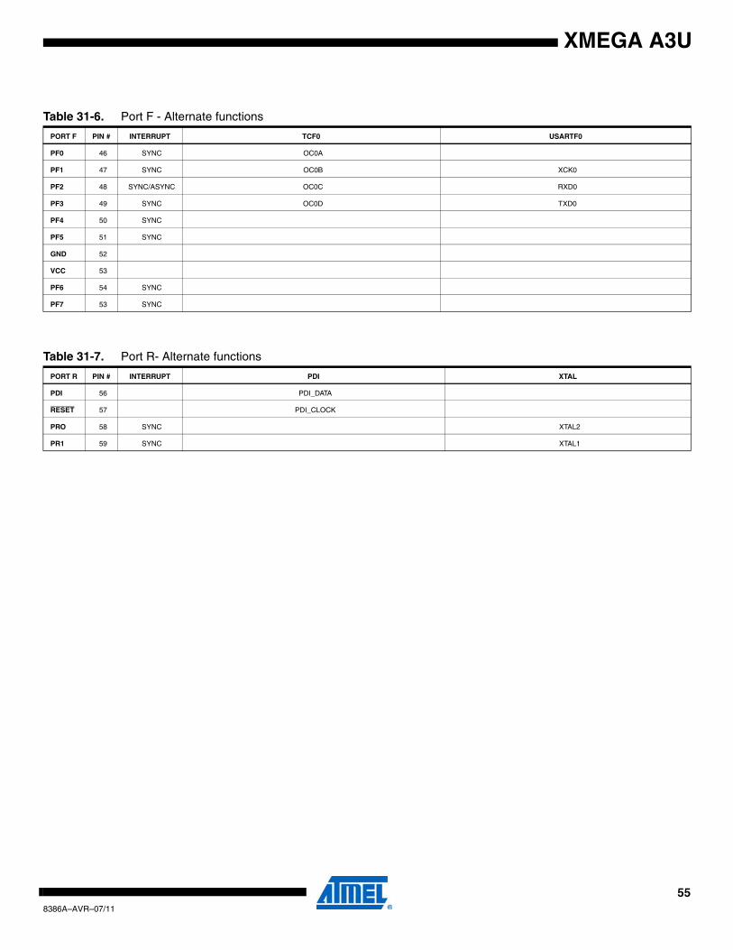
XMEGA A3U
Table 31-6. Port F - Alternate functions
PORT F PIN # INTERRUPT TCF0 USARTF0
PF0 46 SYNC OC0A
PF1 47 SYNC OC0B XCK0
PF2 48 SYNC/ASYNC OC0C RXD0
PF3 49 SYNC OC0D TXD0
PF4 50 SYNC
PF5 51 SYNC
GND 52
VCC 53
PF6 54 SYNC
PF7 53 SYNC
Table 31-7. Port R- Alternate functions
PORT R PIN # INTERRUPT PDI XTAL
PDI 56 PDI_DATA
RESET 57 PDI_CLOCK
PRO 58 SYNC XTAL2
PR1 59 SYNC XTAL1
558386A–AVR–07/11
XMEGA A3U
32. Peripheral Module Address MapThe address maps show the base address for each peripheral and module in XMEGA A3U. Forcomplete register description and summary for each peripheral module, refer to the XMEGA AUManual.
Base Address Name Description
0x0000 GPIO General Purpose IO Registers0x0010 VPORT0 Virtual Port 00x0014 VPORT1 Virtual Port 10x0018 VPORT2 Virtual Port 20x001C VPORT3 Virtual Port 30x0030 CPU CPU0x0040 CLK Clock Control0x0048 SLEEP Sleep Controller0x0050 OSC Oscillator Control0x0060 DFLLRC32M DFLL for the 32MHz Internal Oscillator0x0068 DFLLRC2M DFLL for the 2MHz Internal Oscillator0x0070 PR Power Reduction0x0078 RST Reset Controller0x0080 WDT Watch-Dog Timer0x0090 MCU MCU Control0x00A0 PMIC Programmable Multilevel Interrupt Controller0x00B0 PORTCFG Port Configuration0x00C0 AES AES Module0x00D0 CRC CRC Module0x0100 DMA DMA Controller0x0180 EVSYS Event System0x01C0 NVM Non Volatile Memory (NVM) Controller0x0200 ADCA Analog to Digital Converter on port A0x0240 ADCB Analog to Digital Converter on port B0x0320 DACB Digital to Analog Converter on port B0x0380 ACA Analog Comparator pair on port A0x0390 ACB Analog Comparator pair on port B0x0400 RTC Real Time Counter0x0480 TWIC Two Wire Interface on port C0x04A0 TWIE Two Wire Interface on port E0x04C0 USB USB Device0x0600 PORTA Port A0x0620 PORTB Port B0x0640 PORTC Port C0x0660 PORTD Port D0x0680 PORTE Port E0x06A0 PORTF Port F0x07E0 PORTR Port R0x0800 TCC0 Timer/Counter 0 on port C0x0840 TCC1 Timer/Counter 1 on port C0x0880 AWEXC Advanced Waveform Extension on port C0x0890 HIRESC High Resolution Extension on port C0x08A0 USARTC0 USART 0 on port C0x08B0 USARTC1 USART 1 on port C0x08C0 SPIC Serial Peripheral Interface on port C0x08F8 IRCOM Infrared Communication Module0x0900 TCD0 Timer/Counter 0 on port D0x0940 TCD1 Timer/Counter 1 on port D0x0990 HIRESD High Resolution Extension on port D0x09A0 USARTD0 USART 0 on port D0x09B0 USARTD1 USART 1 on port D0x09C0 SPID Serial Peripheral Interface on port D0x0A00 TCE0 Timer/Counter 0 on port E0x0A40 TCE1 Timer/Counter 1 on port E0x0A80 AWEXE Advanced Waveform Extension on port E0x0A90 HIRESE High Resolution Extension on port E0x0AA0 USARTE0 USART 0 on port E0x0AB0 USARTE1 USART 1 on port E0x0AC0 SPIE Serial Peripheral Interface on port E0x0B00 TCF0 Timer/Counter 0 on port F
568386A–AVR–07/11
XMEGA A3U
0x0B90 HIRESF High Resolution Extension on port F0x0BA0 USARTF0 USART 0 on port F0x0BC0 SPIF Serial Peripheral Interface on port F
Base Address Name Description
578386A–AVR–07/11
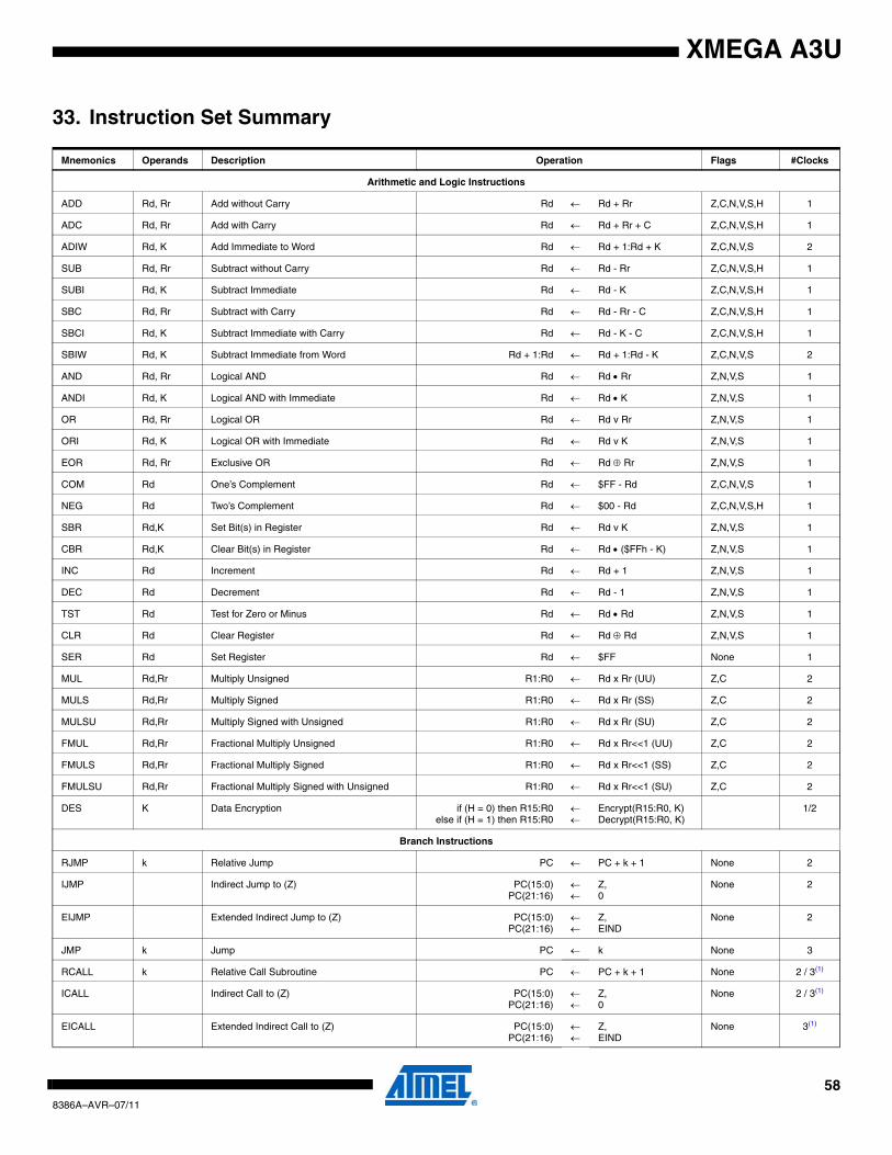
XMEGA A3U
33. Instruction Set Summary
Mnemonics Operands Description Operation Flags #Clocks
Arithmetic and Logic Instructions
ADD Rd, Rr Add without Carry Rd ← Rd + Rr Z,C,N,V,S,H 1
ADC Rd, Rr Add with Carry Rd ← Rd + Rr + C Z,C,N,V,S,H 1
ADIW Rd, K Add Immediate to Word Rd ← Rd + 1:Rd + K Z,C,N,V,S 2
SUB Rd, Rr Subtract without Carry Rd ← Rd - Rr Z,C,N,V,S,H 1
SUBI Rd, K Subtract Immediate Rd ← Rd - K Z,C,N,V,S,H 1
SBC Rd, Rr Subtract with Carry Rd ← Rd - Rr - C Z,C,N,V,S,H 1
SBCI Rd, K Subtract Immediate with Carry Rd ← Rd - K - C Z,C,N,V,S,H 1
SBIW Rd, K Subtract Immediate from Word Rd + 1:Rd ← Rd + 1:Rd - K Z,C,N,V,S 2
AND Rd, Rr Logical AND Rd ← Rd • Rr Z,N,V,S 1
ANDI Rd, K Logical AND with Immediate Rd ← Rd • K Z,N,V,S 1
OR Rd, Rr Logical OR Rd ← Rd v Rr Z,N,V,S 1
ORI Rd, K Logical OR with Immediate Rd ← Rd v K Z,N,V,S 1
EOR Rd, Rr Exclusive OR Rd ← Rd ⊕ Rr Z,N,V,S 1
COM Rd One’s Complement Rd ← $FF - Rd Z,C,N,V,S 1
NEG Rd Two’s Complement Rd ← $00 - Rd Z,C,N,V,S,H 1
SBR Rd,K Set Bit(s) in Register Rd ← Rd v K Z,N,V,S 1
CBR Rd,K Clear Bit(s) in Register Rd ← Rd • ($FFh - K) Z,N,V,S 1
INC Rd Increment Rd ← Rd + 1 Z,N,V,S 1
DEC Rd Decrement Rd ← Rd - 1 Z,N,V,S 1
TST Rd Test for Zero or Minus Rd ← Rd • Rd Z,N,V,S 1
CLR Rd Clear Register Rd ← Rd ⊕ Rd Z,N,V,S 1
SER Rd Set Register Rd ← $FF None 1
MUL Rd,Rr Multiply Unsigned R1:R0 ← Rd x Rr (UU) Z,C 2
MULS Rd,Rr Multiply Signed R1:R0 ← Rd x Rr (SS) Z,C 2
MULSU Rd,Rr Multiply Signed with Unsigned R1:R0 ← Rd x Rr (SU) Z,C 2
FMUL Rd,Rr Fractional Multiply Unsigned R1:R0 ← Rd x Rr<<1 (UU) Z,C 2
FMULS Rd,Rr Fractional Multiply Signed R1:R0 ← Rd x Rr<<1 (SS) Z,C 2
FMULSU Rd,Rr Fractional Multiply Signed with Unsigned R1:R0 ← Rd x Rr<<1 (SU) Z,C 2
DES K Data Encryption if (H = 0) then R15:R0else if (H = 1) then R15:R0
←←
Encrypt(R15:R0, K)Decrypt(R15:R0, K)
1/2
Branch Instructions
RJMP k Relative Jump PC ← PC + k + 1 None 2
IJMP Indirect Jump to (Z) PC(15:0)PC(21:16)
←←
Z,0
None 2
EIJMP Extended Indirect Jump to (Z) PC(15:0)PC(21:16)
←←
Z,EIND
None 2
JMP k Jump PC ← k None 3
RCALL k Relative Call Subroutine PC ← PC + k + 1 None 2 / 3(1)
ICALL Indirect Call to (Z) PC(15:0)PC(21:16)
←←
Z,0
None 2 / 3(1)
EICALL Extended Indirect Call to (Z) PC(15:0)PC(21:16)
←←
Z,EIND
None 3(1)
588386A–AVR–07/11
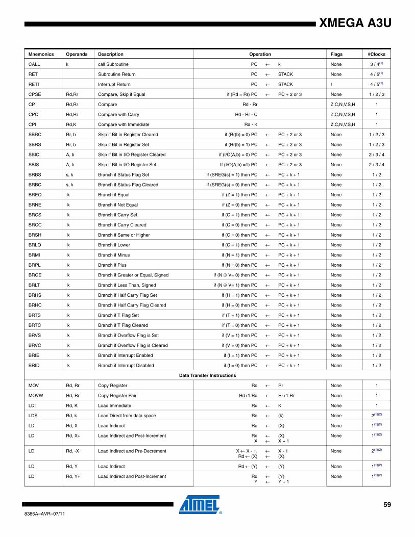
XMEGA A3U
CALL k call Subroutine PC ← k None 3 / 4(1)
RET Subroutine Return PC ← STACK None 4 / 5(1)
RETI Interrupt Return PC ← STACK I 4 / 5(1)
CPSE Rd,Rr Compare, Skip if Equal if (Rd = Rr) PC ← PC + 2 or 3 None 1 / 2 / 3
CP Rd,Rr Compare Rd - Rr Z,C,N,V,S,H 1
CPC Rd,Rr Compare with Carry Rd - Rr - C Z,C,N,V,S,H 1
CPI Rd,K Compare with Immediate Rd - K Z,C,N,V,S,H 1
SBRC Rr, b Skip if Bit in Register Cleared if (Rr(b) = 0) PC ← PC + 2 or 3 None 1 / 2 / 3
SBRS Rr, b Skip if Bit in Register Set if (Rr(b) = 1) PC ← PC + 2 or 3 None 1 / 2 / 3
SBIC A, b Skip if Bit in I/O Register Cleared if (I/O(A,b) = 0) PC ← PC + 2 or 3 None 2 / 3 / 4
SBIS A, b Skip if Bit in I/O Register Set If (I/O(A,b) =1) PC ← PC + 2 or 3 None 2 / 3 / 4
BRBS s, k Branch if Status Flag Set if (SREG(s) = 1) then PC ← PC + k + 1 None 1 / 2
BRBC s, k Branch if Status Flag Cleared if (SREG(s) = 0) then PC ← PC + k + 1 None 1 / 2
BREQ k Branch if Equal if (Z = 1) then PC ← PC + k + 1 None 1 / 2
BRNE k Branch if Not Equal if (Z = 0) then PC ← PC + k + 1 None 1 / 2
BRCS k Branch if Carry Set if (C = 1) then PC ← PC + k + 1 None 1 / 2
BRCC k Branch if Carry Cleared if (C = 0) then PC ← PC + k + 1 None 1 / 2
BRSH k Branch if Same or Higher if (C = 0) then PC ← PC + k + 1 None 1 / 2
BRLO k Branch if Lower if (C = 1) then PC ← PC + k + 1 None 1 / 2
BRMI k Branch if Minus if (N = 1) then PC ← PC + k + 1 None 1 / 2
BRPL k Branch if Plus if (N = 0) then PC ← PC + k + 1 None 1 / 2
BRGE k Branch if Greater or Equal, Signed if (N ⊕ V= 0) then PC ← PC + k + 1 None 1 / 2
BRLT k Branch if Less Than, Signed if (N ⊕ V= 1) then PC ← PC + k + 1 None 1 / 2
BRHS k Branch if Half Carry Flag Set if (H = 1) then PC ← PC + k + 1 None 1 / 2
BRHC k Branch if Half Carry Flag Cleared if (H = 0) then PC ← PC + k + 1 None 1 / 2
BRTS k Branch if T Flag Set if (T = 1) then PC ← PC + k + 1 None 1 / 2
BRTC k Branch if T Flag Cleared if (T = 0) then PC ← PC + k + 1 None 1 / 2
BRVS k Branch if Overflow Flag is Set if (V = 1) then PC ← PC + k + 1 None 1 / 2
BRVC k Branch if Overflow Flag is Cleared if (V = 0) then PC ← PC + k + 1 None 1 / 2
BRIE k Branch if Interrupt Enabled if (I = 1) then PC ← PC + k + 1 None 1 / 2
BRID k Branch if Interrupt Disabled if (I = 0) then PC ← PC + k + 1 None 1 / 2
Data Transfer Instructions
MOV Rd, Rr Copy Register Rd ← Rr None 1
MOVW Rd, Rr Copy Register Pair Rd+1:Rd ← Rr+1:Rr None 1
LDI Rd, K Load Immediate Rd ← K None 1
LDS Rd, k Load Direct from data space Rd ← (k) None 2(1)(2)
LD Rd, X Load Indirect Rd ← (X) None 1(1)(2)
LD Rd, X+ Load Indirect and Post-Increment RdX
←←
(X)X + 1
None 1(1)(2)
LD Rd, -X Load Indirect and Pre-Decrement X ← X - 1,Rd ← (X)
←←
X - 1(X)
None 2(1)(2)
LD Rd, Y Load Indirect Rd ← (Y) ← (Y) None 1(1)(2)
LD Rd, Y+ Load Indirect and Post-Increment RdY
←←
(Y)Y + 1
None 1(1)(2)
Mnemonics Operands Description Operation Flags #Clocks
598386A–AVR–07/11
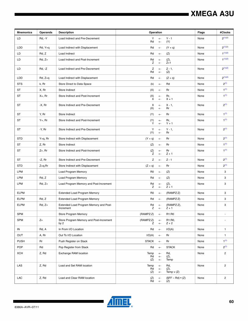
XMEGA A3U
LD Rd, -Y Load Indirect and Pre-Decrement YRd
←←
Y - 1(Y)
None 2(1)(2)
LDD Rd, Y+q Load Indirect with Displacement Rd ← (Y + q) None 2(1)(2)
LD Rd, Z Load Indirect Rd ← (Z) None 1(1)(2)
LD Rd, Z+ Load Indirect and Post-Increment RdZ
←←
(Z),Z+1
None 1(1)(2)
LD Rd, -Z Load Indirect and Pre-Decrement ZRd
←←
Z - 1,(Z)
None 2(1)(2)
LDD Rd, Z+q Load Indirect with Displacement Rd ← (Z + q) None 2(1)(2)
STS k, Rr Store Direct to Data Space (k) ← Rd None 2(1)
ST X, Rr Store Indirect (X) ← Rr None 1(1)
ST X+, Rr Store Indirect and Post-Increment (X)X
←←
Rr,X + 1
None 1(1)
ST -X, Rr Store Indirect and Pre-Decrement X(X)
←←
X - 1,Rr
None 2(1)
ST Y, Rr Store Indirect (Y) ← Rr None 1(1)
ST Y+, Rr Store Indirect and Post-Increment (Y)Y
←←
Rr,Y + 1
None 1(1)
ST -Y, Rr Store Indirect and Pre-Decrement Y(Y)
←←
Y - 1,Rr
None 2(1)
STD Y+q, Rr Store Indirect with Displacement (Y + q) ← Rr None 2(1)
ST Z, Rr Store Indirect (Z) ← Rr None 1(1)
ST Z+, Rr Store Indirect and Post-Increment (Z)Z
←←
RrZ + 1
None 1(1)
ST -Z, Rr Store Indirect and Pre-Decrement Z ← Z - 1 None 2(1)
STD Z+q,Rr Store Indirect with Displacement (Z + q) ← Rr None 2(1)
LPM Load Program Memory R0 ← (Z) None 3
LPM Rd, Z Load Program Memory Rd ← (Z) None 3
LPM Rd, Z+ Load Program Memory and Post-Increment RdZ
←←
(Z),Z + 1
None 3
ELPM Extended Load Program Memory R0 ← (RAMPZ:Z) None 3
ELPM Rd, Z Extended Load Program Memory Rd ← (RAMPZ:Z) None 3
ELPM Rd, Z+ Extended Load Program Memory and Post-Increment
RdZ
←←
(RAMPZ:Z),Z + 1
None 3
SPM Store Program Memory (RAMPZ:Z) ← R1:R0 None -
SPM Z+ Store Program Memory and Post-Increment by 2
(RAMPZ:Z)Z
←←
R1:R0,Z + 2
None -
IN Rd, A In From I/O Location Rd ← I/O(A) None 1
OUT A, Rr Out To I/O Location I/O(A) ← Rr None 1
PUSH Rr Push Register on Stack STACK ← Rr None 1(1)
POP Rd Pop Register from Stack Rd ← STACK None 2(1)
XCH Z, Rd Exchange RAM location TempRd(Z)
←←←
Rd,(Z),Temp
None 2
LAS Z, Rd Load and Set RAM location TempRd(Z)
←←←
Rd,(Z),Temp v (Z)
None 2
LAC Z, Rd Load and Clear RAM location (Z)Rd
←←
($FF – Rd) • (Z)(Z)
None 2
Mnemonics Operands Description Operation Flags #Clocks
608386A–AVR–07/11
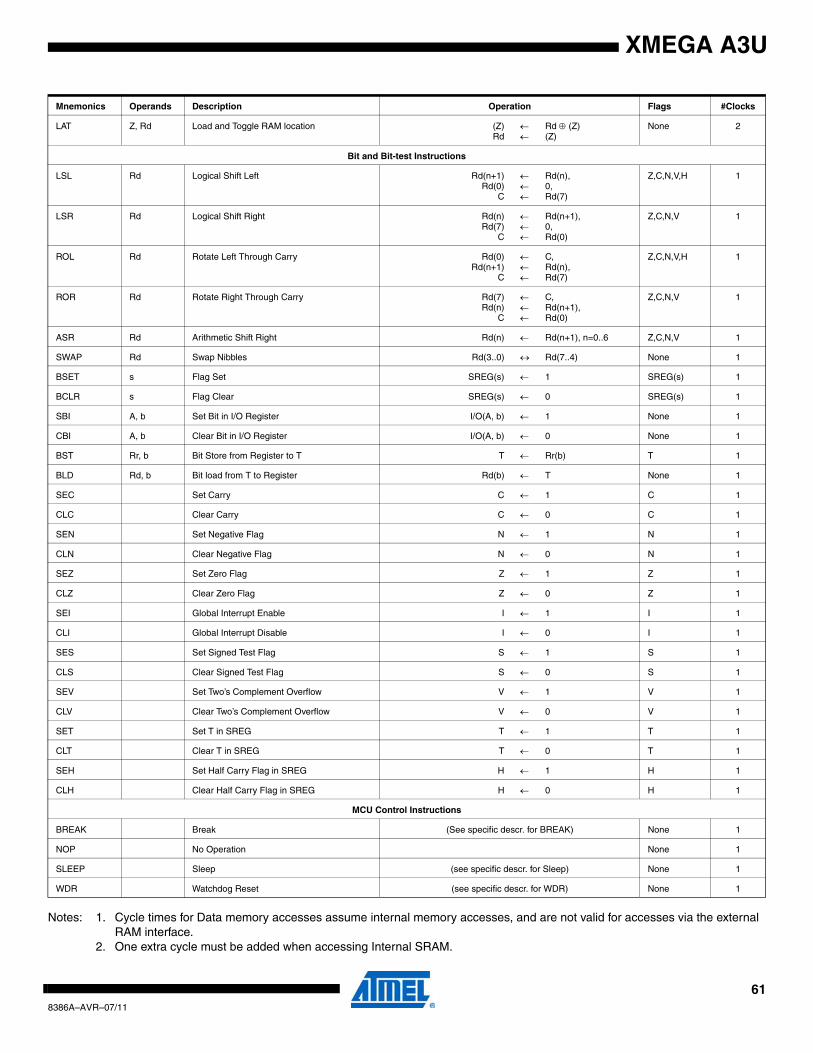
XMEGA A3U
Notes: 1. Cycle times for Data memory accesses assume internal memory accesses, and are not valid for accesses via the external RAM interface.
2. One extra cycle must be added when accessing Internal SRAM.
LAT Z, Rd Load and Toggle RAM location (Z)Rd
←←
Rd ⊕ (Z)(Z)
None 2
Bit and Bit-test Instructions
LSL Rd Logical Shift Left Rd(n+1)Rd(0)
C
←←←
Rd(n),0,Rd(7)
Z,C,N,V,H 1
LSR Rd Logical Shift Right Rd(n)Rd(7)
C
←←←
Rd(n+1),0,Rd(0)
Z,C,N,V 1
ROL Rd Rotate Left Through Carry Rd(0)Rd(n+1)
C
←←←
C,Rd(n),Rd(7)
Z,C,N,V,H 1
ROR Rd Rotate Right Through Carry Rd(7)Rd(n)
C
←←←
C,Rd(n+1),Rd(0)
Z,C,N,V 1
ASR Rd Arithmetic Shift Right Rd(n) ← Rd(n+1), n=0..6 Z,C,N,V 1
SWAP Rd Swap Nibbles Rd(3..0) ↔ Rd(7..4) None 1
BSET s Flag Set SREG(s) ← 1 SREG(s) 1
BCLR s Flag Clear SREG(s) ← 0 SREG(s) 1
SBI A, b Set Bit in I/O Register I/O(A, b) ← 1 None 1
CBI A, b Clear Bit in I/O Register I/O(A, b) ← 0 None 1
BST Rr, b Bit Store from Register to T T ← Rr(b) T 1
BLD Rd, b Bit load from T to Register Rd(b) ← T None 1
SEC Set Carry C ← 1 C 1
CLC Clear Carry C ← 0 C 1
SEN Set Negative Flag N ← 1 N 1
CLN Clear Negative Flag N ← 0 N 1
SEZ Set Zero Flag Z ← 1 Z 1
CLZ Clear Zero Flag Z ← 0 Z 1
SEI Global Interrupt Enable I ← 1 I 1
CLI Global Interrupt Disable I ← 0 I 1
SES Set Signed Test Flag S ← 1 S 1
CLS Clear Signed Test Flag S ← 0 S 1
SEV Set Two’s Complement Overflow V ← 1 V 1
CLV Clear Two’s Complement Overflow V ← 0 V 1
SET Set T in SREG T ← 1 T 1
CLT Clear T in SREG T ← 0 T 1
SEH Set Half Carry Flag in SREG H ← 1 H 1
CLH Clear Half Carry Flag in SREG H ← 0 H 1
MCU Control Instructions
BREAK Break (See specific descr. for BREAK) None 1
NOP No Operation None 1
SLEEP Sleep (see specific descr. for Sleep) None 1
WDR Watchdog Reset (see specific descr. for WDR) None 1
Mnemonics Operands Description Operation Flags #Clocks
618386A–AVR–07/11
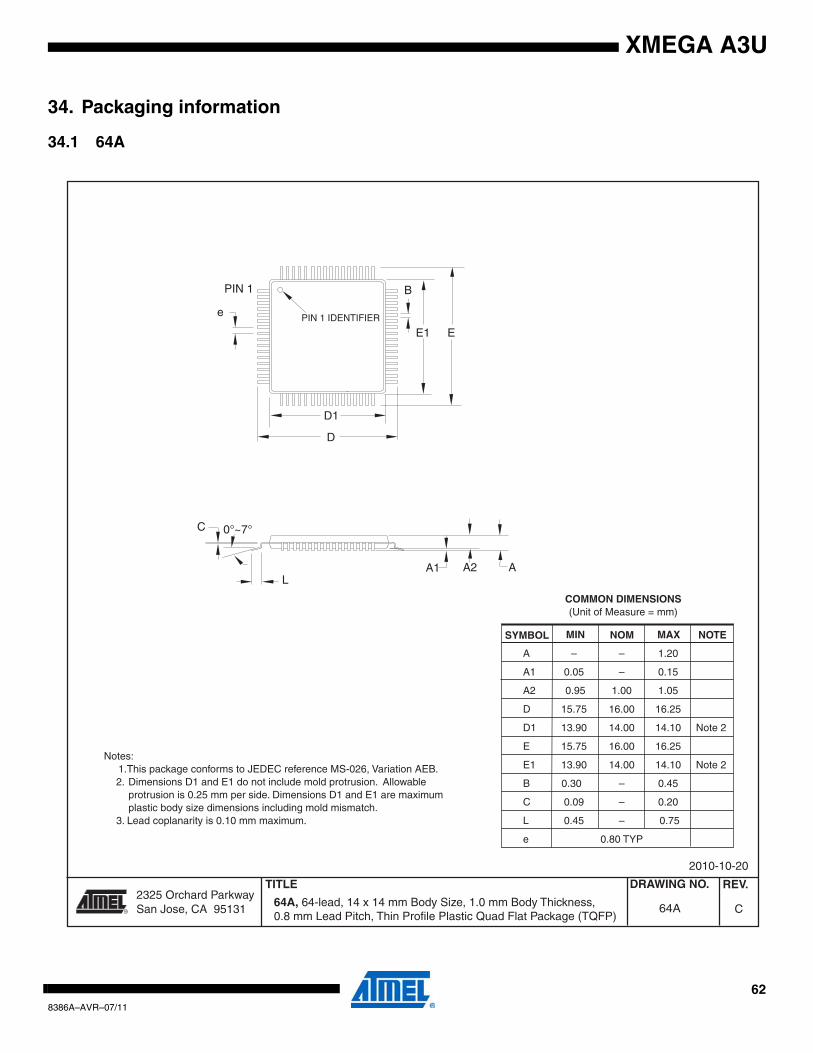
XMEGA A3U
34. Packaging information
34.1 64A
2325 Orchard Parkway San Jose, CA 95131
TITLE DRAWING NO.
R
REV.
64A, 64-lead, 14 x 14 mm Body Size, 1.0 mm Body Thickness,0.8 mm Lead Pitch, Thin Profile Plastic Quad Flat Package (TQFP)
C64A
2010-10-20
PIN 1 IDENTIFIER
0°~7°
PIN 1
L
C
A1 A2 A
D1
D
e
E1 E
B
COMMON DIMENSIONS(Unit of Measure = mm)
SYMBOL MIN NOM MAX NOTE
Notes: 1.This package conforms to JEDEC reference MS-026, Variation AEB. 2. Dimensions D1 and E1 do not include mold protrusion. Allowable protrusion is 0.25 mm per side. Dimensions D1 and E1 are maximum plastic body size dimensions including mold mismatch. 3. Lead coplanarity is 0.10 mm maximum.
A – – 1.20
A1 0.05 – 0.15
A2 0.95 1.00 1.05
D 15.75 16.00 16.25
D1 13.90 14.00 14.10 Note 2
E 15.75 16.00 16.25
E1 13.90 14.00 14.10 Note 2
B 0.30 – 0.45
C 0.09 – 0.20
L 0.45 – 0.75
e 0.80 TYP
628386A–AVR–07/11
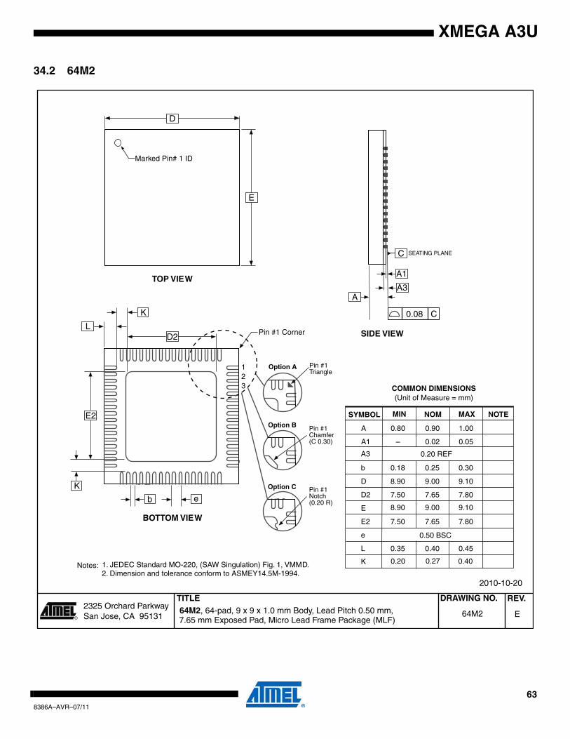
XMEGA A3U
34.2 64M2
2325 Orchard Parkway San Jose, CA 95131
TITLE DRAWING NO.
R
REV. 64M2, 64-pad, 9 x 9 x 1.0 mm Body, Lead Pitch 0.50 mm, E64M2
2010-10-20
COMMON DIMENSIONS(Unit of Measure = mm)
SYMBOL MIN NOM MAX NOTE
A 0.80 0.90 1.00
A1 – 0.02 0.05
b
0.18 0.25 0.30
D
D2
7.50 7.65 7.80
8.90 9.00 9.10
8.90 9.00 9.10
E
E2
7.50 7.65 7.80
e
0.50 BSC
L 0.35 0.40
0.45
TOP VIEW
SIDE VIEW
BOTTOM VIEW
D
E
Marked Pin# 1 ID
SEATING PLANE
A1
C
A
C0.08
123
K 0.20 0.27 0.40
2. Dimension and tolerance conform to ASMEY14.5M-1994.
0.20 REFA3
A3
E2
D2
b e
Pin #1 CornerL
Pin #1 Triangle
Pin #1 Chamfer(C 0.30)
Option A
Option B
Pin #1 Notch(0.20 R)
Option C
K
K
Notes: 1. JEDEC Standard MO-220, (SAW Singulation) Fig. 1, VMMD.
7.65 mm Exposed Pad, Micro Lead Frame Package (MLF)
638386A–AVR–07/11
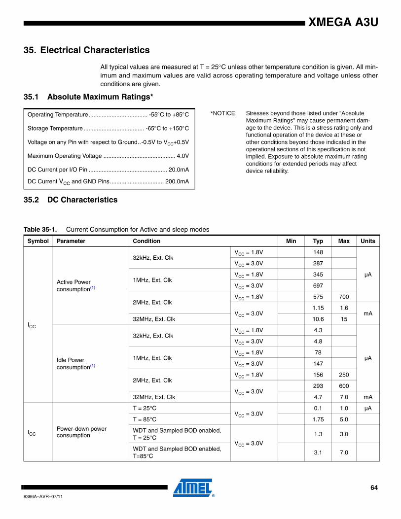
XMEGA A3U
35. Electrical Characteristics
All typical values are measured at T = 25°C unless other temperature condition is given. All min-imum and maximum values are valid across operating temperature and voltage unless otherconditions are given.
35.1 Absolute Maximum Ratings*
35.2 DC Characteristics
Operating Temperature.................................... -55°C to +85°C *NOTICE: Stresses beyond those listed under “Absolute Maximum Ratings” may cause permanent dam-age to the device. This is a stress rating only and functional operation of the device at these or other conditions beyond those indicated in the operational sections of this specification is not implied. Exposure to absolute maximum rating conditions for extended periods may affect device reliability.
Storage Temperature ..................................... -65°C to +150°C
Voltage on any Pin with respect to Ground..-0.5V to VCC+0.5V
Maximum Operating Voltage ............................................ 4.0V
DC Current per I/O Pin ................................................ 20.0mA
DC Current VCC and GND Pins................................. 200.0mA
Table 35-1. Current Consumption for Active and sleep modes
Symbol Parameter Condition Min Typ Max Units
ICC
Active Power consumption(1)
32kHz, Ext. ClkVCC = 1.8V 148
µA
VCC = 3.0V 287
1MHz, Ext. ClkVCC = 1.8V 345
VCC = 3.0V 697
2MHz, Ext. ClkVCC = 1.8V 575 700
VCC = 3.0V1.15 1.6
mA32MHz, Ext. Clk 10.6 15
Idle Power consumption(1)
32kHz, Ext. ClkVCC = 1.8V 4.3
µA
VCC = 3.0V 4.8
1MHz, Ext. ClkVCC = 1.8V 78
VCC = 3.0V 147
2MHz, Ext. ClkVCC = 1.8V 156 250
VCC = 3.0V293 600
32MHz, Ext. Clk 4.7 7.0 mA
ICCPower-down power consumption
T = 25°CVCC = 3.0V
0.1 1.0 µA
T = 85°C 1.75 5.0
WDT and Sampled BOD enabled, T = 25°C
VCC = 3.0V
1.3 3.0
WDT and Sampled BOD enabled, T=85°C
3.1 7.0
648386A–AVR–07/11
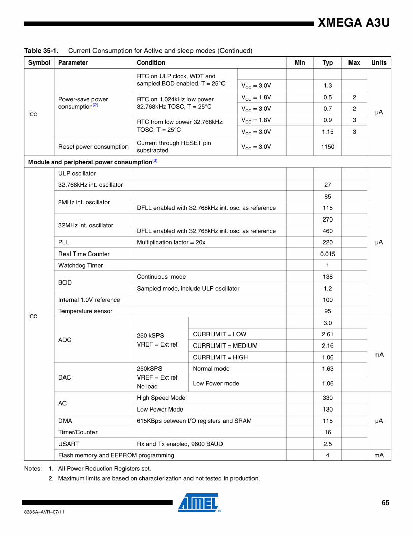
XMEGA A3U
Notes: 1. All Power Reduction Registers set.
2. Maximum limits are based on characterization and not tested in production.
ICC
Power-save power consumption(2)
RTC on ULP clock, WDT and sampled BOD enabled, T = 25°C
µA
VCC = 3.0V 1.3
RTC on 1.024kHz low power 32.768kHz TOSC, T = 25°C
VCC = 1.8V 0.5 2
VCC = 3.0V 0.7 2
RTC from low power 32.768kHz TOSC, T = 25°C
VCC = 1.8V 0.9 3
VCC = 3.0V 1.15 3
Reset power consumptionCurrent through RESET pin substracted
VCC = 3.0V 1150
Module and peripheral power consumption(3)
ICC
ULP oscillator
µA
32.768kHz int. oscillator 27
2MHz int. oscillator85
DFLL enabled with 32.768kHz int. osc. as reference 115
32MHz int. oscillator270
DFLL enabled with 32.768kHz int. osc. as reference 460
PLL Multiplication factor = 20x 220
Real Time Counter 0.015
Watchdog Timer 1
BODContinuous mode 138
Sampled mode, include ULP oscillator 1.2
Internal 1.0V reference 100
Temperature sensor 95
ADC250 kSPS
VREF = Ext ref
3.0
mA
CURRLIMIT = LOW 2.61
CURRLIMIT = MEDIUM 2.16
CURRLIMIT = HIGH 1.06
DAC
250kSPS
VREF = Ext refNo load
Normal mode 1.63
Low Power mode 1.06
ACHigh Speed Mode 330
µA
Low Power Mode 130
DMA 615KBps between I/O registers and SRAM 115
Timer/Counter 16
USART Rx and Tx enabled, 9600 BAUD 2.5
Flash memory and EEPROM programming 4 mA
Table 35-1. Current Consumption for Active and sleep modes (Continued)
Symbol Parameter Condition Min Typ Max Units
658386A–AVR–07/11

XMEGA A3U
3. All parameters measured as the difference in current consumption between module enabled and disabled. All data at VCC = 3.0V, ClkSYS = 1MHz External clock without prescaling, T = 25°C unless other conditiond are given .
35.3 Operating Voltage and Frequency
The maximum System clock frequency of the Atmel® AVR® XMEGA A3U devices is dependingon VCC. As shown in Figure 35-1 on page 66 the Frequency vs. VCC curve is linear between1.8V < VCC < 2.7V.
Figure 35-1. Maximum Frequency vs. Vcc
Table 35-2. Operating voltage and frequency
Symbol Parameter Condition Min Typ Max Units
ClkCPU CPU clock frequency
VCC = 1.6V 0 12
MHzVCC = 1.8V 0 12
VCC = 2.7V 0 32
VCC = 3.6V 0 32
1.8
12
32
MHz
V2.7 3.61.6
Safe Operating Area
668386A–AVR–07/11
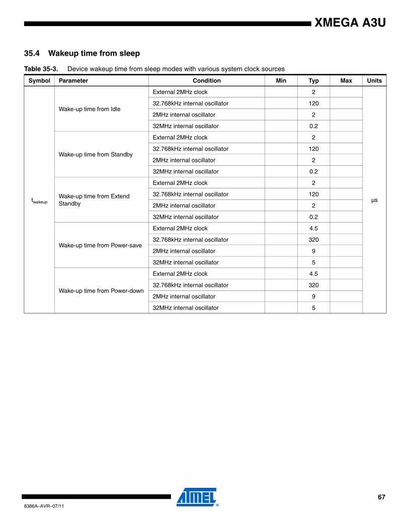
XMEGA A3U
35.4 Wakeup time from sleep
Table 35-3. Device wakeup time from sleep modes with various system clock sources
Symbol Parameter Condition Min Typ Max Units
twakeup
Wake-up time from Idle
External 2MHz clock 2
µs
32.768kHz internal oscillator 120
2MHz internal oscillator 2
32MHz internal oscillator 0.2
Wake-up time from Standby
External 2MHz clock 2
32.768kHz internal oscillator 120
2MHz internal oscillator 2
32MHz internal oscillator 0.2
Wake-up time from Extend Standby
External 2MHz clock 2
32.768kHz internal oscillator 120
2MHz internal oscillator 2
32MHz internal oscillator 0.2
Wake-up time from Power-save
External 2MHz clock 4.5
32.768kHz internal oscillator 320
2MHz internal oscillator 9
32MHz internal oscillator 5
Wake-up time from Power-down
External 2MHz clock 4.5
32.768kHz internal oscillator 320
2MHz internal oscillator 9
32MHz internal oscillator 5
678386A–AVR–07/11
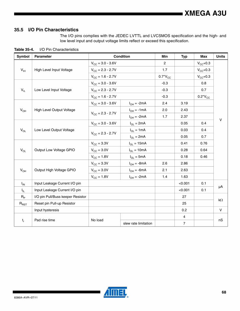
XMEGA A3U
35.5 I/O Pin Characteristics The I/O pins complies with the JEDEC LVTTL and LVCSMOS specification and the high- andlow level input and output voltage limits reflect or exceed this specification.
Table 35-4. I/O Pin Characteristics
Symbol Parameter Condition Min Typ Max Units
VIH High Level Input Voltage
VCC = 3.0 - 3.6V 2 VCC+0.3
V
VCC = 2.3 - 2.7V 1.7 VCC+0.3
VCC = 1.6 - 2.7V 0.7*VCC VCC+0.3
VIL Low Level Input Voltage
VCC = 3.0 - 3.6V -0.3 0.8
VCC = 2.3 - 2.7V -0.3 0.7
VCC = 1.6 - 2.7V -0.3 0.2*VCC
VOH High Level Output Voltage
VCC = 3.0 - 3.6V IOH = -2mA 2.4 3.19
VCC = 2.3 - 2.7VIOH = -1mA 2.0 2.43
IOH = -2mA 1.7 2.37
VOL Low Level Output Voltage
VCC = 3.0 - 3.6V IOL = 2mA 0.05 0.4
VCC = 2.3 - 2.7VIOL = 1mA 0.03 0.4
IOL = 2mA 0.05 0.7
VOL Output Low Voltage GPIO
VCC = 3.3V IOL = 15mA 0.41 0.76
VCC = 3.0V IOL = 10mA 0.28 0.64
VCC = 1.8V IOL = 5mA 0.18 0.46
VOH Output High Voltage GPIO
VCC = 3.3V IOH = -8mA 2.6 2.86
VCC = 3.0V IOH = -6mA 2.1 2.63
VCC = 1.8V IOH = -2mA 1.4 1.63
IIN Input Leakage Current I/O pin <0.001 0.1µA
IIL Input Leakage Current I/O pin <0.001 0.1
RP I/O pin Pull/Buss keeper Resistor 27kΩ
RRST Reset pin Pull-up Resistor 25
Input hysteresis 0.2 V
tr Pad rise time No load4
nSslew rate limitation 7
688386A–AVR–07/11
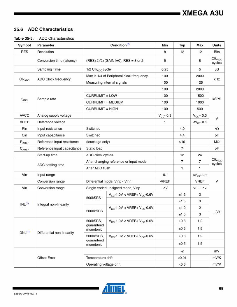
XMEGA A3U
35.6 ADC Characteristics
Table 35-5. ADC Characteristics
Symbol Parameter Condition(2) Min Typ Max Units
RES Resolution 8 12 12 Bits
Conversion time (latency) (RES+2)/2+(GAIN !=0), RES = 8 or 2 5 8ClkADCcycles
Sampling Time 1/2 ClkADC cycle 0.25 5 µS
ClkADC ADC Clock frequencyMax is 1/4 of Peripheral clock frequency 100 2000
kHzMeasuring internal signals 100 125
fADC Sample rate
100 2000
kSPSCURRLIMIT = LOW 100 1500
CURRLIMIT = MEDIUM 100 1000
CURRLIMIT = HIGH 100 500
AVCC Analog supply voltage VCC- 0.3 VCC+ 0.3V
VREF Reference voltage 1 AVCC- 0.6
Rin Input resistance Switched 4.0 kΩ
Cin Input capacitance Switched 4.4 pF
RAREF Reference input resistance (leackage only) >10 MΩ
CAREF Reference input capacitance Static load 7 pF
Start-up time ADC clock cycles 12 24ClkADCcyclesADC settling time
After changing reference or input mode 7 7
After ADC flush 1 1
Vin Input range -0.1 AVCC+ 0.1
VConversion range Differential mode, Vinp - Vinn -VREF VREF
Vin Conversion range Single ended unsigned mode, Vinp -ΔV VREF-ΔV
INL(1) Integral non-linearity
500kSPSVCC-1.0V < VREF< VCC-0.6V ±1.2 2
LSB
±1.5 3
2000kSPSVCC-1.0V < VREF< VCC-0.6V ±1.0 2
±1.5 3
DNL(1) Differential non-linearity
500kSPS,guaranteedmonotonic
VCC-1.0V < VREF< VCC-0.6V ±0.8 1.2
±0.5 1.5
2000kSPS,guaranteedmonotonic
VCC-1.0V < VREF< VCC-0.6V ±0.8 1.2
±0.5 1.5
Offset Error
-2 mV
Temperature drift <0.01 mV/K
Operating voltage drift <0.6 mV/V
698386A–AVR–07/11
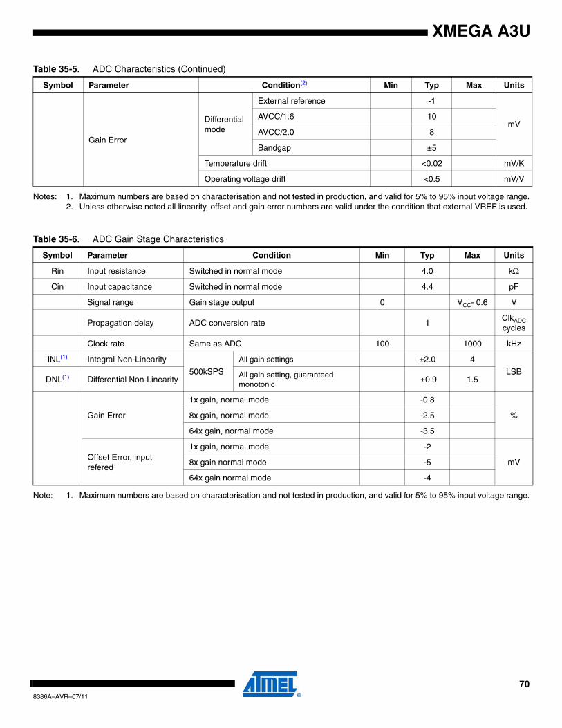
XMEGA A3U
Notes: 1. Maximum numbers are based on characterisation and not tested in production, and valid for 5% to 95% input voltage range.2. Unless otherwise noted all linearity, offset and gain error numbers are valid under the condition that external VREF is used.
Note: 1. Maximum numbers are based on characterisation and not tested in production, and valid for 5% to 95% input voltage range.
Gain Error
Differential mode
External reference -1
mVAVCC/1.6 10
AVCC/2.0 8
Bandgap ±5
Temperature drift <0.02 mV/K
Operating voltage drift <0.5 mV/V
Table 35-5. ADC Characteristics (Continued)
Symbol Parameter Condition(2) Min Typ Max Units
Table 35-6. ADC Gain Stage Characteristics
Symbol Parameter Condition Min Typ Max Units
Rin Input resistance Switched in normal mode 4.0 kΩ
Cin Input capacitance Switched in normal mode 4.4 pF
Signal range Gain stage output 0 VCC- 0.6 V
Propagation delay ADC conversion rate 1ClkADCcycles
Clock rate Same as ADC 100 1000 kHz
INL(1) Integral Non-Linearity
500kSPS
All gain settings ±2.0 4
LSBDNL(1) Differential Non-Linearity
All gain setting, guaranteed monotonic
±0.9 1.5
Gain Error
1x gain, normal mode -0.8
%8x gain, normal mode -2.5
64x gain, normal mode -3.5
Offset Error, input refered
1x gain, normal mode -2
mV8x gain normal mode -5
64x gain normal mode -4
708386A–AVR–07/11
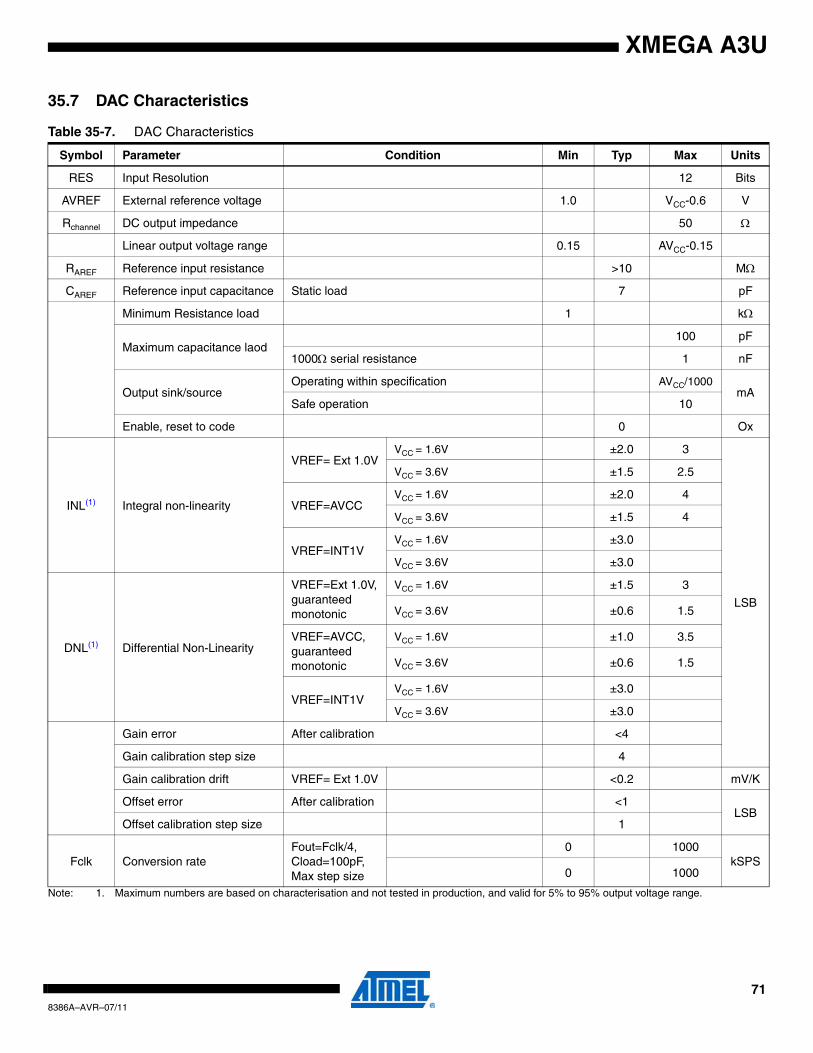
XMEGA A3U
35.7 DAC Characteristics
Note: 1. Maximum numbers are based on characterisation and not tested in production, and valid for 5% to 95% output voltage range.
Table 35-7. DAC Characteristics
Symbol Parameter Condition Min Typ Max Units
RES Input Resolution 12 Bits
AVREF External reference voltage 1.0 VCC-0.6 V
Rchannel DC output impedance 50 Ω
Linear output voltage range 0.15 AVCC-0.15
RAREF Reference input resistance >10 MΩ
CAREF Reference input capacitance Static load 7 pF
Minimum Resistance load 1 kΩ
Maximum capacitance laod100 pF
1000Ω serial resistance 1 nF
Output sink/sourceOperating within specification AVCC/1000
mASafe operation 10
Enable, reset to code 0 Ox
INL(1) Integral non-linearity
VREF= Ext 1.0VVCC = 1.6V ±2.0 3
LSB
VCC = 3.6V ±1.5 2.5
VREF=AVCCVCC = 1.6V ±2.0 4
VCC = 3.6V ±1.5 4
VREF=INT1VVCC = 1.6V ±3.0
VCC = 3.6V ±3.0
DNL(1) Differential Non-Linearity
VREF=Ext 1.0V,guaranteedmonotonic
VCC = 1.6V ±1.5 3
VCC = 3.6V ±0.6 1.5
VREF=AVCC,guaranteedmonotonic
VCC = 1.6V ±1.0 3.5
VCC = 3.6V ±0.6 1.5
VREF=INT1VVCC = 1.6V ±3.0
VCC = 3.6V ±3.0
Gain error After calibration <4
Gain calibration step size 4
Gain calibration drift VREF= Ext 1.0V <0.2 mV/K
Offset error After calibration <1LSB
Offset calibration step size 1
Fclk Conversion rateFout=Fclk/4,Cload=100pF,Max step size
0 1000kSPS
0 1000
718386A–AVR–07/11
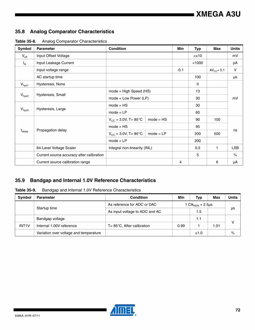
XMEGA A3U
35.8 Analog Comparator Characteristics
35.9 Bandgap and Internal 1.0V Reference Characteristics
Table 35-8. Analog Comparator Characteristics
Symbol Parameter Condition Min Typ Max Units
Voff Input Offset Voltage <±10 mV
Ilk Input Leakage Current <1000 pA
Input voltage range -0.1 AVCC+ 0.1 V
AC startup time 100 µs
Vhys1 Hysteresis, None 0
mVVhys2 Hysteresis, Small
mode = High Speed (HS) 13
mode = Low Power (LP) 30
Vhys3 Hysteresis, Largemode = HS 30
mode = LP 60
tdelay Propagation delay
VCC = 3.0V, T= 85°C mode = HS 90 100
nsmode = HS 95
VCC = 3.0V, T= 85°C mode = LP 200 500
mode = LP 200
64-Level Voltage Scaler Integral non-linearity (INL) 0.5 1 LSB
Current source accuracy after calibration 5 %
Current source calibration range 4 6 µA
Table 35-9. Bandgap and Internal 1.0V Reference Characteristics
Symbol Parameter Condition Min Typ Max Units
Startup timeAs reference for ADC or DAC 1 ClkPER + 2.5µs
µsAs input voltage to ADC and AC 1.5
Bandgap voltage 1.1V
INT1V Internal 1.00V reference T= 85°C, After calibration 0.99 1 1.01
Variation over voltage and temperature ±1.0 %
728386A–AVR–07/11
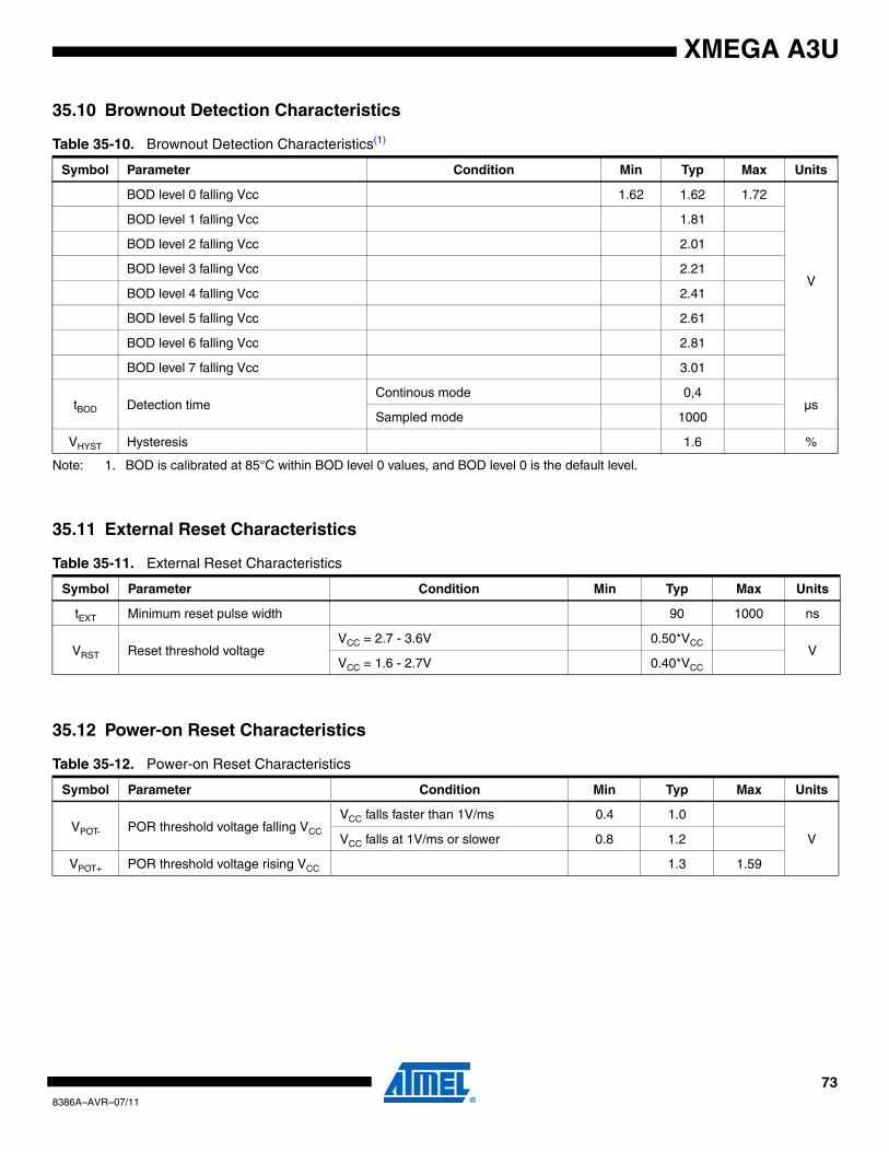
XMEGA A3U
35.10 Brownout Detection Characteristics
Note: 1. BOD is calibrated at 85°C within BOD level 0 values, and BOD level 0 is the default level.
35.11 External Reset Characteristics
35.12 Power-on Reset Characteristics
Table 35-10. Brownout Detection Characteristics(1)
Symbol Parameter Condition Min Typ Max Units
BOD level 0 falling Vcc 1.62 1.62 1.72
V
BOD level 1 falling Vcc 1.81
BOD level 2 falling Vcc 2.01
BOD level 3 falling Vcc 2.21
BOD level 4 falling Vcc 2.41
BOD level 5 falling Vcc 2.61
BOD level 6 falling Vcc 2.81
BOD level 7 falling Vcc 3.01
tBOD Detection timeContinous mode 0,4
µsSampled mode 1000
VHYST Hysteresis 1.6 %
Table 35-11. External Reset Characteristics
Symbol Parameter Condition Min Typ Max Units
tEXT Minimum reset pulse width 90 1000 ns
VRST Reset threshold voltageVCC = 2.7 - 3.6V 0.50*VCC
VVCC = 1.6 - 2.7V 0.40*VCC
Table 35-12. Power-on Reset Characteristics
Symbol Parameter Condition Min Typ Max Units
VPOT- POR threshold voltage falling VCC
VCC falls faster than 1V/ms 0.4 1.0
VVCC falls at 1V/ms or slower 0.8 1.2
VPOT+ POR threshold voltage rising VCC 1.3 1.59
738386A–AVR–07/11
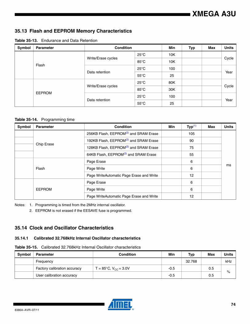
XMEGA A3U
35.13 Flash and EEPROM Memory Characteristics
Notes: 1. Programming is timed from the 2MHz internal oscillator.
2. EEPROM is not erased if the EESAVE fuse is programmed.
35.14 Clock and Oscillator Characteristics
35.14.1 Calibrated 32.768kHz Internal Oscillator characteristics
Table 35-13. Endurance and Data Retention
Symbol Parameter Condition Min Typ Max Units
Flash
Write/Erase cycles25°C 10K
Cycle85°C 10K
Data retention25°C 100
Year55°C 25
EEPROM
Write/Erase cycles25°C 80K
Cycle85°C 30K
Data retention25°C 100
Year55°C 25
Table 35-14. Programming time
Symbol Parameter Condition Min Typ(1) Max Units
Chip Erase
256KB Flash, EEPROM(2) and SRAM Erase 105
ms
192KB Flash, EEPROM(2) and SRAM Erase 90
128KB Flash, EEPROM(2) and SRAM Erase 75
64KB Flash, EEPROM(2) and SRAM Erase 55
Flash
Page Erase 6
Page Write 6
Page WriteAutomatic Page Erase and Write 12
EEPROM
Page Erase 6
Page Write 6
Page WriteAutomatic Page Erase and Write 12
Table 35-15. Calibrated 32.768kHz Internal Oscillator characteristics
Symbol Parameter Condition Min Typ Max Units
Frequency 32.768 kHz
Factory calibration accuracy T = 85°C, VCC = 3.0V -0.5 0.5%
User calibration accuracy -0.5 0.5
748386A–AVR–07/11
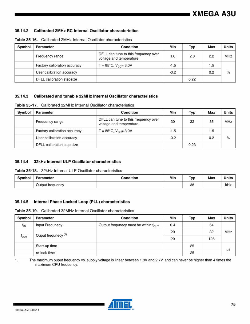
XMEGA A3U
35.14.2 Calibrated 2MHz RC Internal Oscillator characteristics
35.14.3 Calibrated and tunable 32MHz Internal Oscillator characteristics
35.14.4 32kHz Internal ULP Oscillator characteristics
35.14.5 Internal Phase Locked Loop (PLL) characteristics
Table 35-16. Calibrated 2MHz Internal Oscillator characteristics
Symbol Parameter Condition Min Typ Max Units
Frequency rangeDFLL can tune to this frequency over voltage and temperature
1.8 2.0 2.2 MHz
Factory calibration accuracy T = 85°C, VCC= 3.0V -1.5 1.5
%User calibration accuracy -0.2 0.2
DFLL calibration stepsize 0.22
Table 35-17. Calibrated 32MHz Internal Oscillator characteristics
Symbol Parameter Condition Min Typ Max Units
Frequency rangeDFLL can tune to this frequency over voltage and temperature
30 32 55 MHz
Factory calibration accuracy T = 85°C, VCC= 3.0V -1.5 1.5
%User calibration accuracy -0.2 0.2
DFLL calibration step size 0.23
Table 35-18. 32kHz Internal ULP Oscillator characteristics
Symbol Parameter Condition Min Typ Max Units
Output frequency 38 kHz
Table 35-19. Calibrated 32MHz Internal Oscillator characteristics
Symbol Parameter Condition Min Typ Max Units
fIN Input Frequnecy Output frequnecy must be within fOUT 0.4 64
MHzfOUT Ouput frequnecy (1)
1. The maximum ouput frequency vs. supply voltage is linear between 1.8V and 2.7V, and can never be higher than 4 times the maximum CPU frequency.
20 32
20 128
Start-up time 25µs
re-lock time 25
758386A–AVR–07/11

XMEGA A3U
35.14.6 External 32.768kHz Crystal Oscillator and TOSC characteristics
Note: 1. See Figure 35-2 on page 76 for definition
Figure 35-2. TOSC input capacitance
The input capacitance between the TOSC pins is CL1 + CL2 in series as seen from the crystalwhen oscillating without external capacitors.
35.14.7 External Clock Characteristics
Figure 35-3. External Clock Drive Waveform
Table 35-20. External 32.768kHz Crystal Oscillator and TOSC characteristics
Symbol Parameter Condition Min Typ Max Units
ESR/R1Recommended crystal equivalent series resistance (ESR)
Crystal load capacitance 6.5pF 60kΩ
Crystal load capacitance 9.0pF 35
CIN_TOSC Input capacitance between TOSC pinsNormal mode 1.7
pFLow power mode 2.2
Recommended Safety factorcapacitance load matched to crystal specification
3
CL1 CL2
2CSOT1CSOT Device internalExternal
32.768 KHz crystal
tCH
tCL
tCK
tCH
VIL1
VIH1
tCR tCF
768386A–AVR–07/11
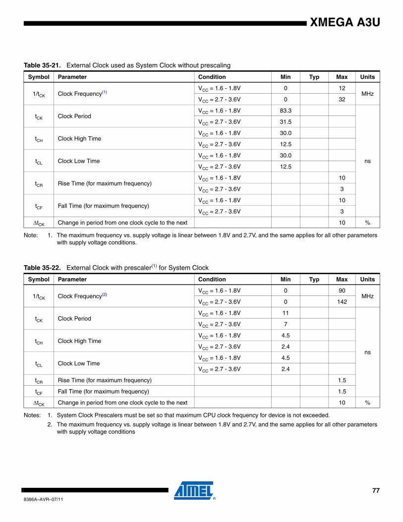
XMEGA A3U
Note: 1. The maximum frequency vs. supply voltage is linear between 1.8V and 2.7V, and the same applies for all other parameters with supply voltage conditions.
Notes: 1. System Clock Prescalers must be set so that maximum CPU clock frequency for device is not exceeded.
2. The maximum frequency vs. supply voltage is linear between 1.8V and 2.7V, and the same applies for all other parameters with supply voltage conditions
Table 35-21. External Clock used as System Clock without prescaling
Symbol Parameter Condition Min Typ Max Units
1/tCK Clock Frequency(1)VCC = 1.6 - 1.8V 0 12
MHzVCC = 2.7 - 3.6V 0 32
tCK Clock PeriodVCC = 1.6 - 1.8V 83.3
ns
VCC = 2.7 - 3.6V 31.5
tCH Clock High TimeVCC = 1.6 - 1.8V 30.0
VCC = 2.7 - 3.6V 12.5
tCL Clock Low TimeVCC = 1.6 - 1.8V 30.0
VCC = 2.7 - 3.6V 12.5
tCR Rise Time (for maximum frequency)VCC = 1.6 - 1.8V 10
VCC = 2.7 - 3.6V 3
tCF Fall Time (for maximum frequency)VCC = 1.6 - 1.8V 10
VCC = 2.7 - 3.6V 3
ΔtCK Change in period from one clock cycle to the next 10 %
Table 35-22. External Clock with prescaler(1) for System Clock
Symbol Parameter Condition Min Typ Max Units
1/tCK Clock Frequency(2)VCC = 1.6 - 1.8V 0 90
MHzVCC = 2.7 - 3.6V 0 142
tCK Clock PeriodVCC = 1.6 - 1.8V 11
ns
VCC = 2.7 - 3.6V 7
tCH Clock High TimeVCC = 1.6 - 1.8V 4.5
VCC = 2.7 - 3.6V 2.4
tCL Clock Low TimeVCC = 1.6 - 1.8V 4.5
VCC = 2.7 - 3.6V 2.4
tCR Rise Time (for maximum frequency) 1.5
tCF Fall Time (for maximum frequency) 1.5
ΔtCK Change in period from one clock cycle to the next 10 %
778386A–AVR–07/11
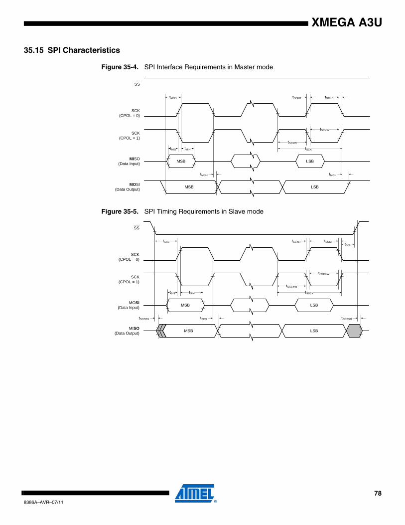
XMEGA A3U
35.15 SPI Characteristics
Figure 35-4. SPI Interface Requirements in Master mode
Figure 35-5. SPI Timing Requirements in Slave mode
MSB LSB
MSB LSB
tMOS
tMIS tMIH
tSCKW
tSCK
tMOH tMOH
tSCKFtSCKR
tSCKW
MOSI(Data Output)
MISO(Data Input)
SCK(CPOL = 1)
SCK(CPOL = 0)
SS
MSB LSB
MSB LSB
tSIS tSIH
tSSCKW
tSSCKW
tSSCK
tSSH
tSOSSH
tSCKR tSCKF
tSOS
tSSS
tSOSSS
MISO(Data Output)
MOSI(Data Input)
SCK(CPOL = 1)
SCK(CPOL = 0)
SS
788386A–AVR–07/11
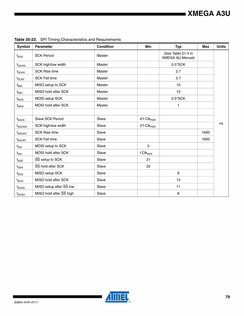
XMEGA A3U
Table 35-23. SPI Timing Characteristics and Requirements
Symbol Parameter Condition Min Typ Max Units
tSCK SCK Period Master(See Table 21-4 in
XMEGA AU Manual)
ns
tSCKW SCK high/low width Master 0.5*SCK
tSCKR SCK Rise time Master 2.7
tSCKF SCK Fall time Master 2.7
tMIS MISO setup to SCK Master 10
tMIH MISO hold after SCK Master 10
tMOS MOSI setup SCK Master 0.5*SCK
tMOH MOSI hold after SCK Master 1
tSSCK Slave SCK Period Slave 4*t ClkPER
tSSCKW SCK high/low width Slave 2*t ClkPER
tSSCKR SCK Rise time Slave 1600
tSSCKF SCK Fall time Slave 1600
tSIS MOSI setup to SCK Slave 3
tSIH MOSI hold after SCK Slave t ClkPER
tSSS SS setup to SCK Slave 21
tSSH SS hold after SCK Slave 20
tSOS MISO setup SCK Slave 8
tSOH MISO hold after SCK Slave 13
tSOSS MISO setup after SS low Slave 11
tSOSH MISO hold after SS high Slave 8
798386A–AVR–07/11
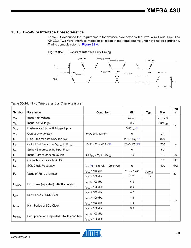
XMEGA A3U
35.16 Two-Wire Interface CharacteristicsTable 2-1 describes the requirements for devices connected to the Two Wire Serial Bus. TheXMEGA Two-Wire Interface meets or exceeds these requirements under the noted conditions.Timing symbols refer to Figure 35-6.
Figure 35-6. Two-Wire Interface Bus Timing
tHD;STA
tof
SDA
SCL
tLOWtHIGH
tSU;STA
tBUF
tr
tHD;DAT tSU;DATtSU;STO
Table 35-24. Two Wire Serial Bus Characteristics
Symbol Parameter Condition Min Typ MaxUnit
s
VIH Input High Voltage 0.7VCC VCC+0.5
VVIL Input Low Voltage 0.5 0.3*VCC
Vhys Hysteresis of Schmitt Trigger Inputs 0.05VCC(1)
VOL Output Low Voltage 3mA, sink current 0 0.4
tr Rise Time for both SDA and SCL 20+0.1Cb(1)(2) 300
nstof Output Fall Time from VIHmin to VILmax 10pF < Cb < 400pF(2) 20+0.1Cb(1)(2) 250
tSP Spikes Suppressed by Input Filter 0 50
II Input Current for each I/O Pin 0.1VCC < VI < 0.9VCC -10 10 µA
CI Capacitance for each I/O Pin 10 pF
fSCL SCL Clock Frequency fPER(3)>max(10fSCL, 250kHz) 0 400 kHz
RP Value of Pull-up resistorfSCL ≤ 100kHz
ΩfSCL > 100kHz
tHD;STA Hold Time (repeated) START conditionfSCL ≤ 100kHz 4.0
µs
fSCL > 100kHz 0.6
tLOW Low Period of SCL ClockfSCL ≤ 100kHz 4.7
fSCL > 100kHz 1.3
tHIGH High Period of SCL ClockfSCL ≤ 100kHz 4.0
fSCL > 100kHz 0.6
tSU;STA Set-up time for a repeated START conditionfSCL ≤ 100kHz
fSCL > 100kHz
VCC 0.4V–
3mA----------------------------
300msCb
-----------------
808386A–AVR–07/11
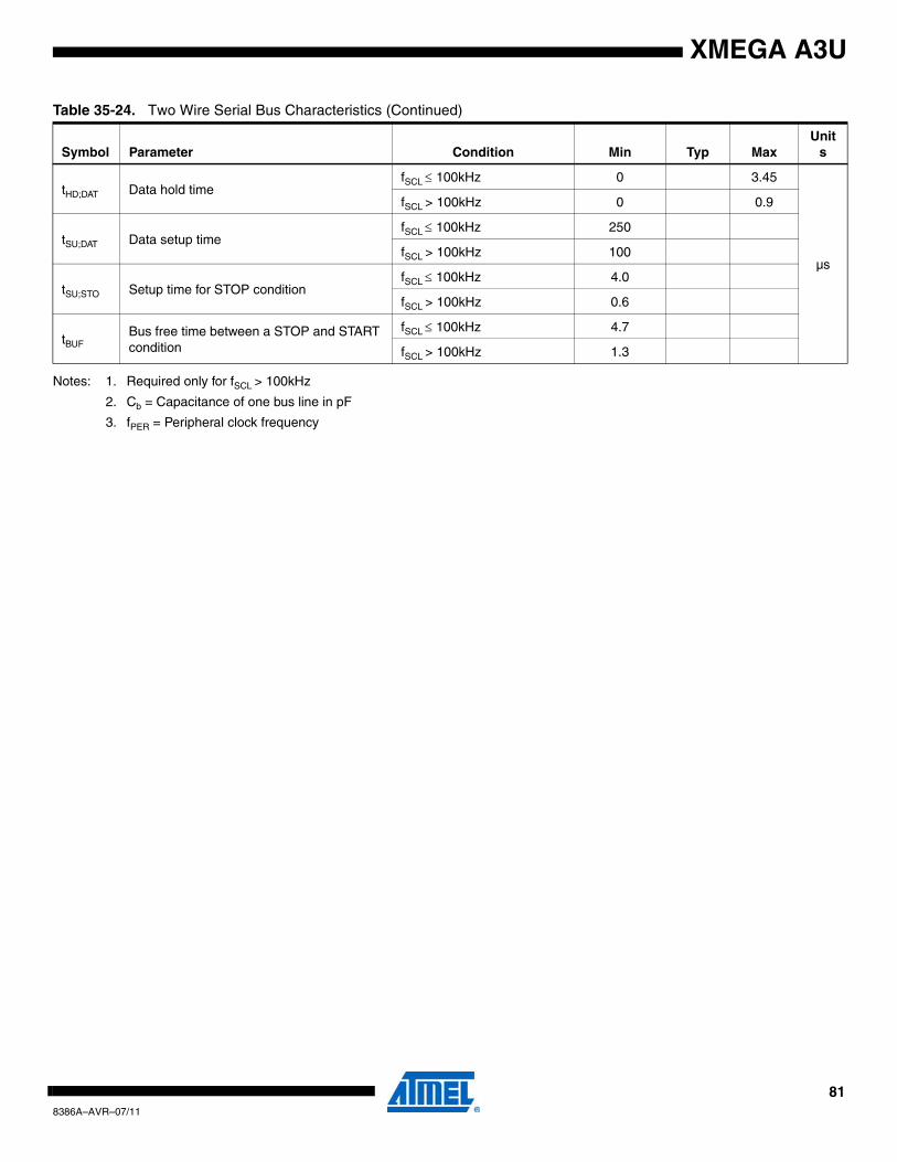
XMEGA A3U
Notes: 1. Required only for fSCL > 100kHz
2. Cb = Capacitance of one bus line in pF
3. fPER = Peripheral clock frequency
tHD;DAT Data hold timefSCL ≤ 100kHz 0 3.45
µs
fSCL > 100kHz 0 0.9
tSU;DAT Data setup timefSCL ≤ 100kHz 250
fSCL > 100kHz 100
tSU;STO Setup time for STOP conditionfSCL ≤ 100kHz 4.0
fSCL > 100kHz 0.6
tBUFBus free time between a STOP and START condition
fSCL ≤ 100kHz 4.7
fSCL > 100kHz 1.3
Table 35-24. Two Wire Serial Bus Characteristics (Continued)
Symbol Parameter Condition Min Typ MaxUnit
s
818386A–AVR–07/11
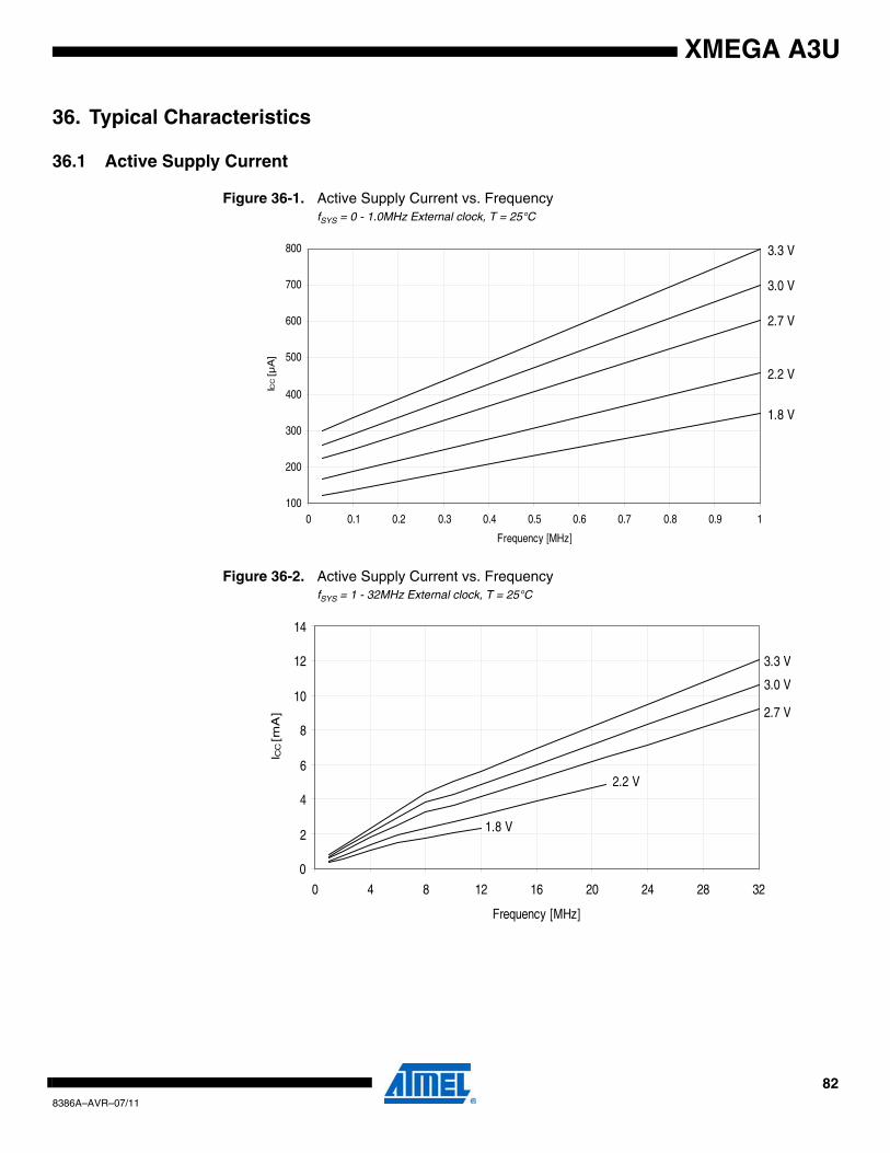
XMEGA A3U
36. Typical Characteristics
36.1 Active Supply Current
Figure 36-1. Active Supply Current vs. FrequencyfSYS = 0 - 1.0MHz External clock, T = 25°C
Figure 36-2. Active Supply Current vs. FrequencyfSYS = 1 - 32MHz External clock, T = 25°C
3.3 V
3.0 V
2.7 V
2.2 V
1.8 V
100
200
300
400
500
600
700
800
0 0.1 0.2 0.3 0.4 0.5 0.6 0.7 0.8 0.9 1
Frequency [MHz]
ICC [µA
]
3.3 V
3.0 V
2.7 V
0
2
4
6
8
10
12
14
0 4 8 12 16 20 24 28 32
Frequency [MHz]
I CC
[mA
]
2.2 V
1.8 V
828386A–AVR–07/11
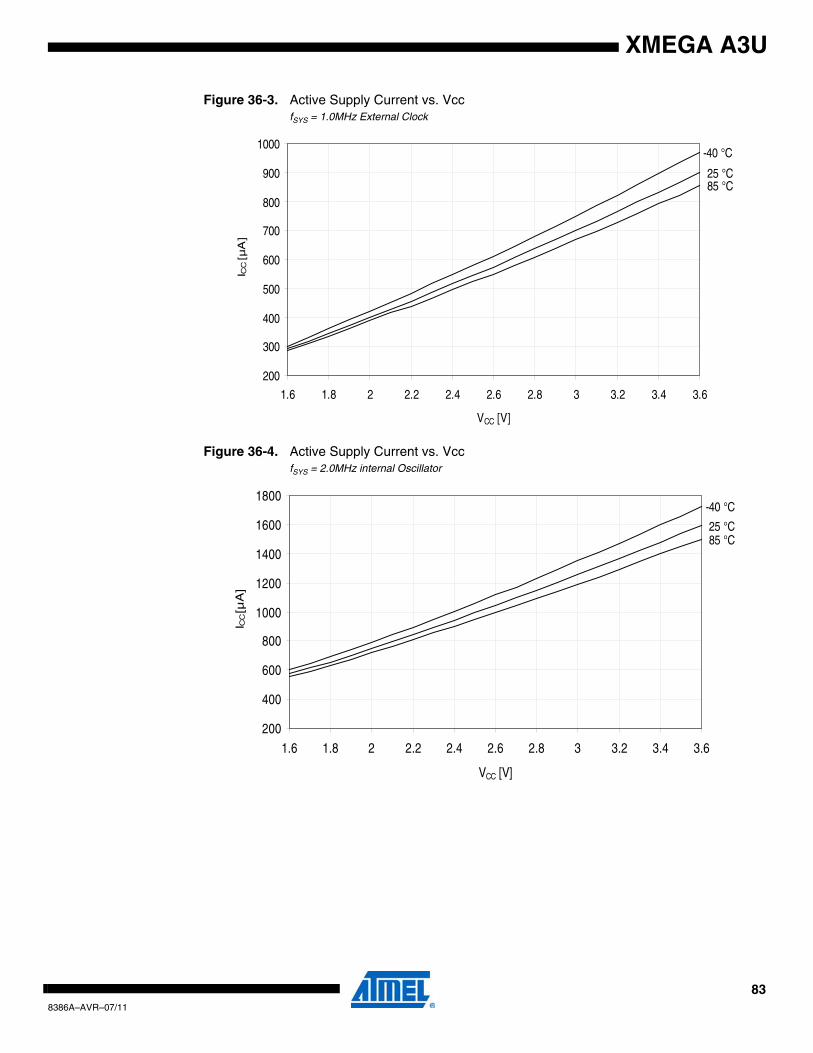
XMEGA A3U
Figure 36-3. Active Supply Current vs. VccfSYS = 1.0MHz External Clock
Figure 36-4. Active Supply Current vs. VccfSYS = 2.0MHz internal Oscillator
85 °C25 °C
-40 °C
200
300
400
500
600
700
800
900
1000
1.6 1.8 2 2.2 2.4 2.6 2.8 3 3.2 3.4 3.6
VCC [V]
I CC
[µA
]
85 °C25 °C
-40 °C
200
400
600
800
1000
1200
1400
1600
1800
1.6 1.8 2 2.2 2.4 2.6 2.8 3 3.2 3.4 3.6
VCC [V]
I CC
[µA
]
838386A–AVR–07/11
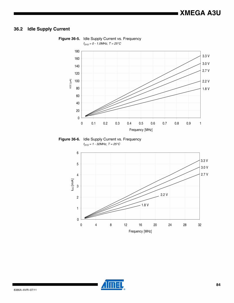
XMEGA A3U
36.2 Idle Supply Current
Figure 36-5. Idle Supply Current vs. FrequencyfSYS = 0 - 1.0MHz, T = 25°C
Figure 36-6. Idle Supply Current vs. FrequencyfSYS = 1 - 32MHz, T = 25°C
3.3 V
3.0 V
2.7 V
2.2 V
1.8 V
0
20
40
60
80
100
120
140
160
180
0 0.1 0.2 0.3 0.4 0.5 0.6 0.7 0.8 0.9 1
Frequency [MHz]
ICC
[µ
A]
3.3 V
3.0 V
2.7 V
0
1
2
3
4
5
6
0 4 8 12 16 20 24 28 32
Frequency [MHz]
I CC
[mA
]
2.2 V
1.8 V
848386A–AVR–07/11
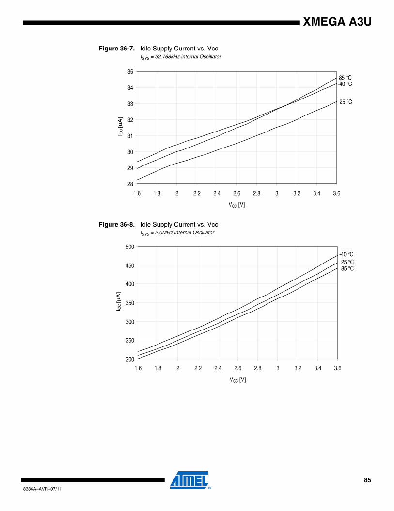
XMEGA A3U
Figure 36-7. Idle Supply Current vs. VccfSYS = 32.768kHz internal Oscillator
Figure 36-8. Idle Supply Current vs. VccfSYS = 2.0MHz internal Oscillator
85 °C
25 °C
-40 °C
28
29
30
31
32
33
34
35
1.6 1.8 2 2.2 2.4 2.6 2.8 3 3.2 3.4 3.6
VCC [V]
I CC
[uA
]
85 °C25 °C
-40 °C
200
250
300
350
400
450
500
1.6 1.8 2 2.2 2.4 2.6 2.8 3 3.2 3.4 3.6
VCC [V]
I CC
[µA
]
858386A–AVR–07/11
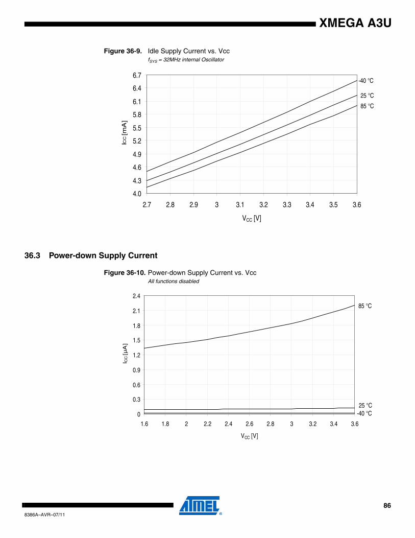
XMEGA A3U
Figure 36-9. Idle Supply Current vs. VccfSYS = 32MHz internal Oscillator
36.3 Power-down Supply Current
Figure 36-10. Power-down Supply Current vs. VccAll functions disabled
85 °C
25 °C
-40 °C
4.0
4.3
4.6
4.9
5.2
5.5
5.8
6.1
6.4
6.7
2.7 2.8 2.9 3 3.1 3.2 3.3 3.4 3.5 3.6
VCC [V]
ICC [m
A]
85 °C
25 °C-40 °C0
0.3
0.6
0.9
1.2
1.5
1.8
2.1
2.4
1.6 1.8 2 2.2 2.4 2.6 2.8 3 3.2 3.4 3.6
VCC [V]
I CC
[µA
]
868386A–AVR–07/11
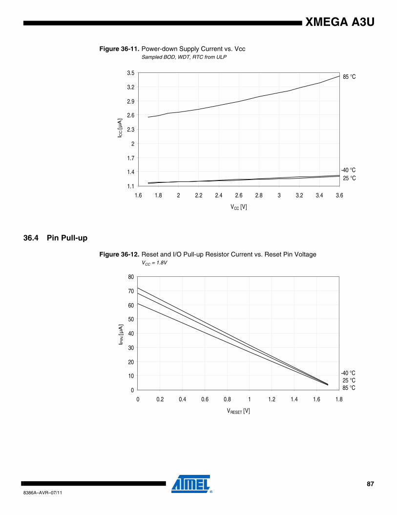
XMEGA A3U
Figure 36-11. Power-down Supply Current vs. VccSampled BOD, WDT, RTC from ULP
36.4 Pin Pull-up
Figure 36-12. Reset and I/O Pull-up Resistor Current vs. Reset Pin VoltageVCC = 1.8V
85 °C
25 °C-40 °C
1.1
1.4
1.7
2
2.3
2.6
2.9
3.2
3.5
1.6 1.8 2 2.2 2.4 2.6 2.8 3 3.2 3.4 3.6
VCC [V]
I CC
[µA
]
85 °C25 °C
-40 °C
0
10
20
30
40
50
60
70
80
0 0.2 0.4 0.6 0.8 1 1.2 1.4 1.6 1.8
VRESET [V]
I PIN [
µA
]
878386A–AVR–07/11
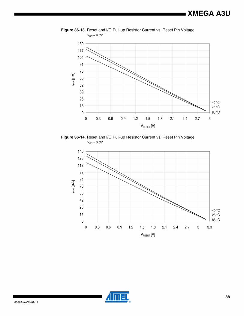
XMEGA A3U
Figure 36-13. Reset and I/O Pull-up Resistor Current vs. Reset Pin VoltageVCC = 3.0V
Figure 36-14. Reset and I/O Pull-up Resistor Current vs. Reset Pin VoltageVCC = 3.3V
85 °C25 °C
-40 °C
0
13
26
39
52
65
78
91
104
117
130
0 0.3 0.6 0.9 1.2 1.5 1.8 2.1 2.4 2.7 3
VRESET [V]
I PIN [
µA
]
85 °C25 °C
-40 °C
0
14
28
42
56
70
84
98
112
126
140
0 0.3 0.6 0.9 1.2 1.5 1.8 2.1 2.4 2.7 3 3.3
VRESET [V]
I PIN
[µ
A]
888386A–AVR–07/11
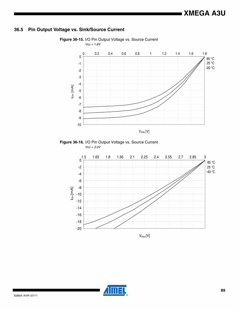
XMEGA A3U
36.5 Pin Output Voltage vs. Sink/Source Current
Figure 36-15. I/O Pin Output Voltage vs. Source CurrentVcc = 1.8V
Figure 36-16. I/O Pin Output Voltage vs. Source CurrentVcc = 3.0V
85 °C25 °C
-20 °C
-10
-9
-8
-7
-6
-5
-4
-3
-2
-1
00 0.2 0.4 0.6 0.8 1 1.2 1.4 1.6 1.8
VPIN [V]
I OH [
mA
]
85 °C25 °C-40 °C
-20
-18
-16
-14
-12
-10
-8
-6
-4
-2
01.5 1.65 1.8 1.95 2.1 2.25 2.4 2.55 2.7 2.85 3
VPIN [V]
I OH
[mA
]
898386A–AVR–07/11

XMEGA A3U
Figure 36-17. I/O Pin Output Voltage vs. Source CurrentVcc = 3.3V
Figure 36-18. I/O Pin Output Voltage vs. Source CurrentT = 25°C
85 °C25 °C-40 °C
-20
-18
-16
-14
-12
-10
-8
-6
-4
-2
01.8 1.95 2.1 2.25 2.4 2.55 2.7 2.85 3 3.15 3.3
VPIN [V]
I OH
[mA
]
3.6 V
3.3 V
2.7 V
2.2 V
1.8 V
0
0.3
0.6
0.9
1.2
1.5
1.8
2.1
2.4
2.7
3
3.3
3.6
-20 -18 -16 -14 -12 -10 -8 -6 -4 -2 0
IPIN [mA]
VP
IN [
V]
908386A–AVR–07/11
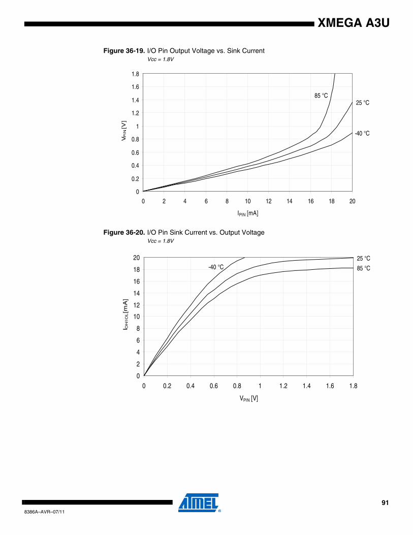
XMEGA A3U
Figure 36-19. I/O Pin Output Voltage vs. Sink CurrentVcc = 1.8V
Figure 36-20. I/O Pin Sink Current vs. Output VoltageVcc = 1.8V
25 °C
-40 °C
0
0.2
0.4
0.6
0.8
1
1.2
1.4
1.6
1.8
0 2 4 6 8 10 12 14 16 18 20
IPIN [mA]
VP
IN[V
]
85 °C
85 °C
25 °C
0
2
4
6
8
10
12
14
16
18
20
0 0.2 0.4 0.6 0.8 1 1.2 1.4 1.6 1.8
VPIN [V]
I OH
/IO
L [m
A]
-40 °C
918386A–AVR–07/11
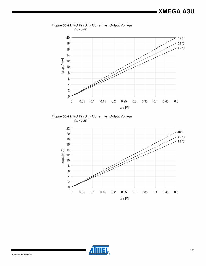
XMEGA A3U
Figure 36-21. I/O Pin Sink Current vs. Output VoltageVcc = 3.0V
Figure 36-22. I/O Pin Sink Current vs. Output VoltageVcc = 3.3V
85 °C
25 °C
-40 °C
0
2
4
6
8
10
12
14
16
18
20
0 0.05 0.1 0.15 0.2 0.25 0.3 0.35 0.4 0.45 0.5
VPIN [V]
I OH
/IO
L [m
A]
85 °C25 °C
-40 °C
0
2
4
6
8
10
12
14
16
18
20
22
0 0.05 0.1 0.15 0.2 0.25 0.3 0.35 0.4 0.45 0.5
VPIN [V]
I OH
/IO
L [m
A]
928386A–AVR–07/11
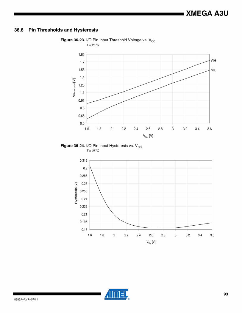
XMEGA A3U
36.6 Pin Thresholds and Hysteresis
Figure 36-23. I/O Pin Input Threshold Voltage vs. VCCT = 25°C
Figure 36-24. I/O Pin Input Hysteresis vs. VCCT = 25°C
VIL
VIH
0.5
0.65
0.8
0.95
1.1
1.25
1.4
1.55
1.7
1.85
1.6 1.8 2 2.2 2.4 2.6 2.8 3 3.2 3.4 3.6
VCC [V]
VTh
resh
old [
V]
0.18
0.195
0.21
0.225
0.24
0.255
0.27
0.285
0.3
0.315
1.6 1.8 2 2.2 2.4 2.6 2.8 3 3.2 3.4 3.6
VCC [V]
Hyste
resis
[V
]
938386A–AVR–07/11
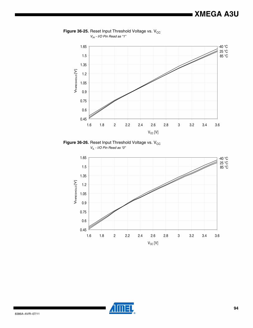
XMEGA A3U
Figure 36-25. Reset Input Threshold Voltage vs. VCC VIH - I/O Pin Read as “1”
Figure 36-26. Reset Input Threshold Voltage vs. VCCVIL - I/O Pin Read as “0”
85 °C25 °C
-40 °C
0.45
0.6
0.75
0.9
1.05
1.2
1.35
1.5
1.65
1.6 1.8 2 2.2 2.4 2.6 2.8 3 3.2 3.4 3.6
VCC [V]
VT
HR
ES
HO
LD
[V]
85 °C25 °C
-40 °C
0.45
0.6
0.75
0.9
1.05
1.2
1.35
1.5
1.65
1.6 1.8 2 2.2 2.4 2.6 2.8 3 3.2 3.4 3.6
VCC [V]
VT
HR
ES
HO
LD
[V]
948386A–AVR–07/11
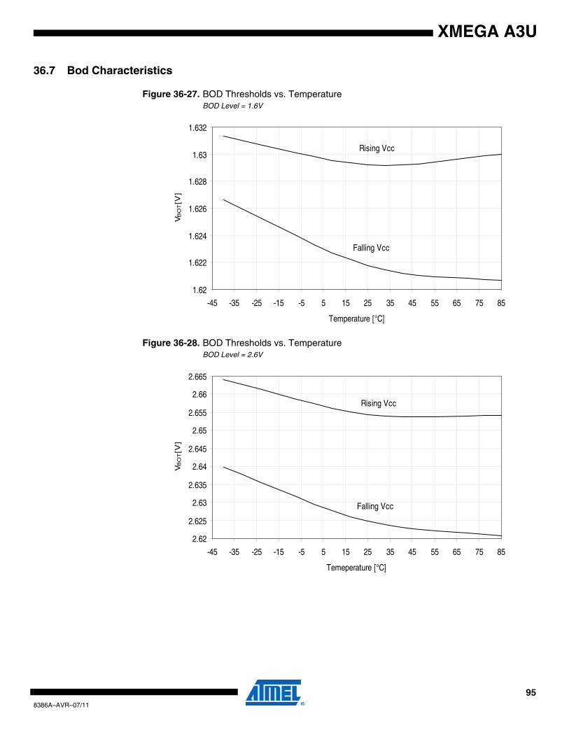
XMEGA A3U
36.7 Bod Characteristics
Figure 36-27. BOD Thresholds vs. TemperatureBOD Level = 1.6V
Figure 36-28. BOD Thresholds vs. TemperatureBOD Level = 2.6V
Rising Vcc
Falling Vcc
1.62
1.622
1.624
1.626
1.628
1.63
1.632
-45 -35 -25 -15 -5 5 15 25 35 45 55 65 75 85
Temperature [°C]
VB
OT [
V]
Rising Vcc
Falling Vcc
2.62
2.625
2.63
2.635
2.64
2.645
2.65
2.655
2.66
2.665
-45 -35 -25 -15 -5 5 15 25 35 45 55 65 75 85
Temeperature [°C]
VB
OT [
V]
958386A–AVR–07/11
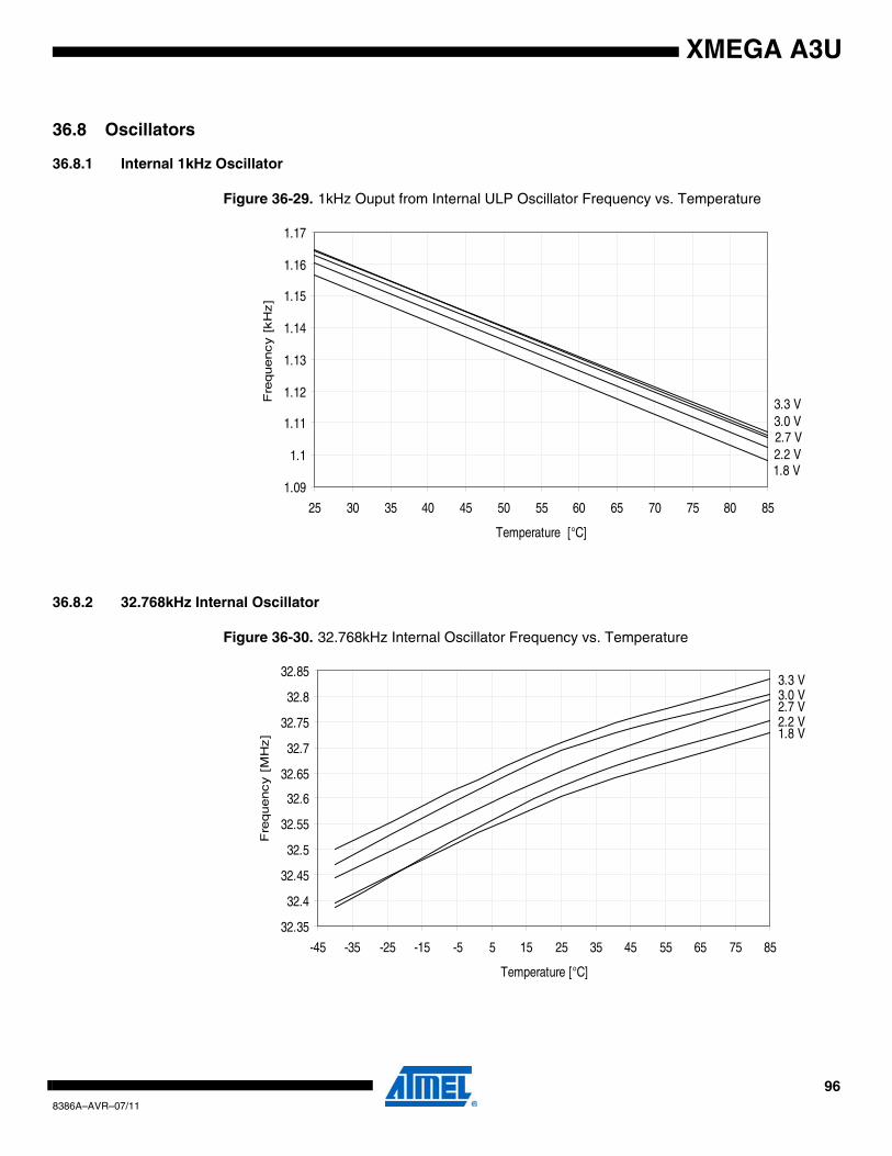
XMEGA A3U
36.8 Oscillators
36.8.1 Internal 1kHz Oscillator
Figure 36-29. 1kHz Ouput from Internal ULP Oscillator Frequency vs. Temperature
36.8.2 32.768kHz Internal Oscillator
Figure 36-30. 32.768kHz Internal Oscillator Frequency vs. Temperature
3.3 V3.0 V2.7 V2.2 V1.8 V
1.09
1.1
1.11
1.12
1.13
1.14
1.15
1.16
1.17
25 30 35 40 45 50 55 60 65 70 75 80 85
Temperature [°C]
Fre
quency [
kH
z]
3.3 V3.0 V2.7 V2.2 V1.8 V
32.35
32.4
32.45
32.5
32.55
32.6
32.65
32.7
32.75
32.8
32.85
-45 -35 -25 -15 -5 5 15 25 35 45 55 65 75 85
Temperature [°C]
Fre
quency [
MH
z]
968386A–AVR–07/11
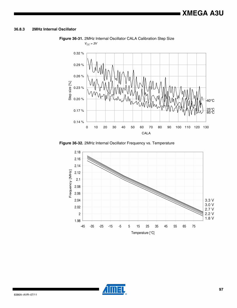
XMEGA A3U
36.8.3 2MHz Internal Oscillator
Figure 36-31. 2MHz Internal Oscillator CALA Calibration Step SizeVCC = 3V
Figure 36-32. 2MHz Internal Oscillator Frequency vs. Temperature
85°C25°C
-40°C
0.14 %
0.17 %
0.20 %
0.23 %
0.26 %
0.29 %
0.32 %
0 10 20 30 40 50 60 70 80 90 100 110 120 130
CALA
Ste
p s
ize
[%]
1.98
2
2.02
2.04
2.06
2.08
2.1
2.12
2.14
2.16
2.18
-45 -35 -25 -15 -5 5 15 25 35 45 55 65 75
Temperature [°C]
Fre
quency [
MH
z]
3.3 V3.0 V2.7 V2.2 V1.8 V
978386A–AVR–07/11
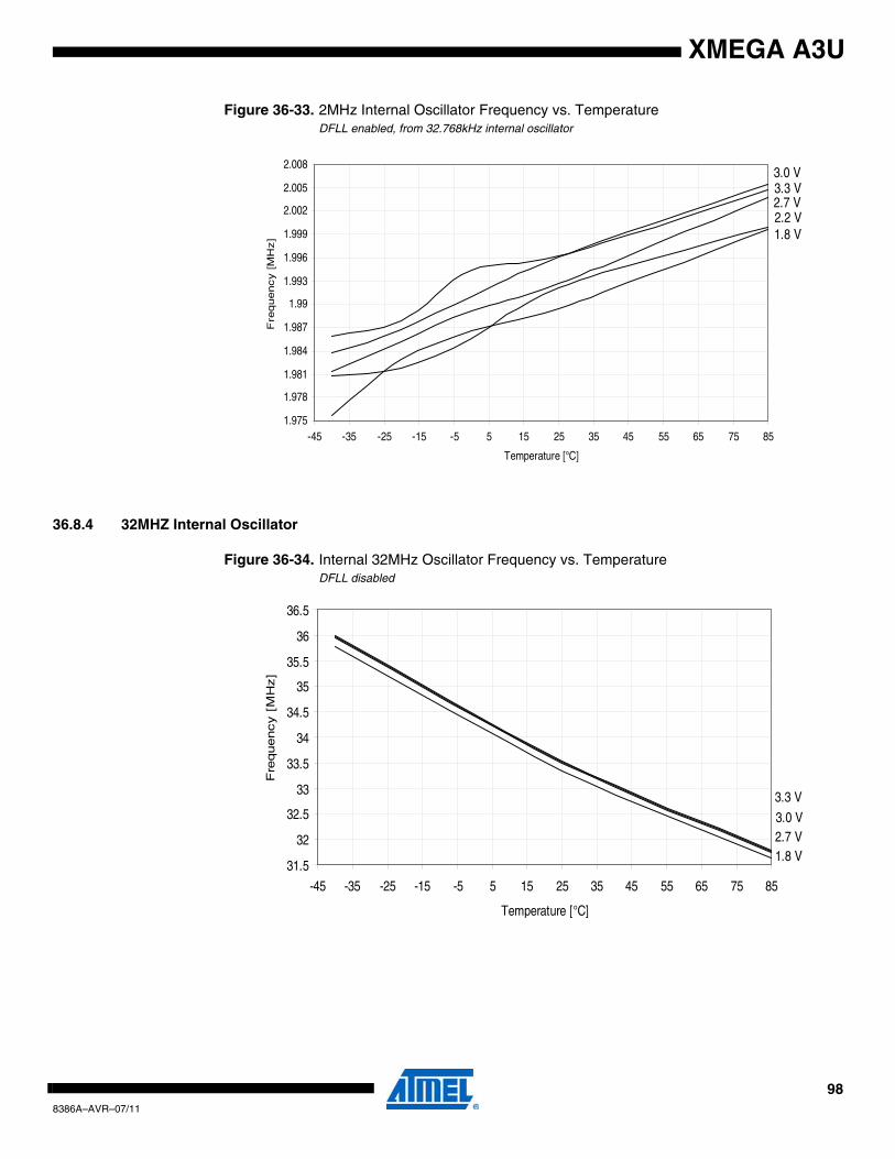
XMEGA A3U
Figure 36-33. 2MHz Internal Oscillator Frequency vs. TemperatureDFLL enabled, from 32.768kHz internal oscillator
36.8.4 32MHZ Internal Oscillator
Figure 36-34. Internal 32MHz Oscillator Frequency vs. TemperatureDFLL disabled
3.3 V3.0 V
2.7 V2.2 V1.8 V
1.975
1.978
1.981
1.984
1.987
1.99
1.993
1.996
1.999
2.002
2.005
2.008
-45 -35 -25 -15 -5 5 15 25 35 45 55 65 75 85
Temperature [°C]
Fre
quency [M
Hz]
3.3 V
3.0 V2.7 V1.8 V
31.5
32
32.5
33
33.5
34
34.5
35
35.5
36
36.5
-45 -35 -25 -15 -5 5 15 25 35 45 55 65 75 85
Temperature [°C]
Fre
quency [
MH
z]
988386A–AVR–07/11
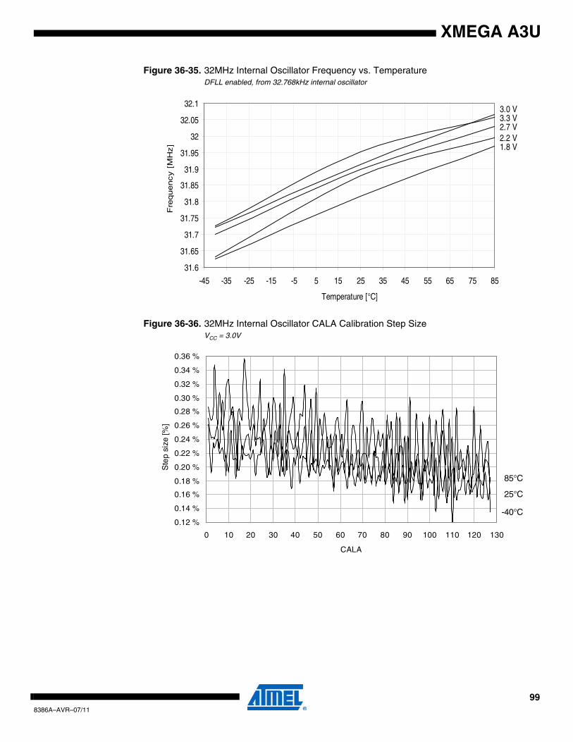
XMEGA A3U
Figure 36-35. 32MHz Internal Oscillator Frequency vs. TemperatureDFLL enabled, from 32.768kHz internal oscillator
Figure 36-36. 32MHz Internal Oscillator CALA Calibration Step SizeVCC = 3.0V
3.3 V3.0 V
2.7 V2.2 V1.8 V
31.6
31.65
31.7
31.75
31.8
31.85
31.9
31.95
32
32.05
32.1
-45 -35 -25 -15 -5 5 15 25 35 45 55 65 75 85
Temperature [°C]
Fre
quency [
MH
z]
85°C
25°C
-40°C0.12 %
0.14 %
0.16 %
0.18 %
0.20 %
0.22 %
0.24 %
0.26 %
0.28 %
0.30 %
0.32 %
0.34 %
0.36 %
0 10 20 30 40 50 60 70 80 90 100 110 120 130
CALA
Ste
p s
ize
[%]
998386A–AVR–07/11
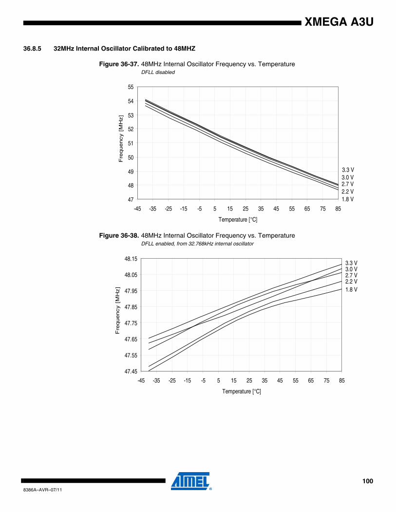
XMEGA A3U
36.8.5 32MHz Internal Oscillator Calibrated to 48MHZ
Figure 36-37. 48MHz Internal Oscillator Frequency vs. TemperatureDFLL disabled
Figure 36-38. 48MHz Internal Oscillator Frequency vs. TemperatureDFLL enabled, from 32.768kHz internal oscillator
3.3 V3.0 V2.7 V2.2 V1.8 V47
48
49
50
51
52
53
54
55
-45 -35 -25 -15 -5 5 15 25 35 45 55 65 75 85
Temperature [°C]
Fre
quency [
MH
z]
3.3 V3.0 V2.7 V2.2 V1.8 V
47.45
47.55
47.65
47.75
47.85
47.95
48.05
48.15
-45 -35 -25 -15 -5 5 15 25 35 45 55 65 75 85
Temperature [°C]
Fre
quency [
MH
z]
1008386A–AVR–07/11
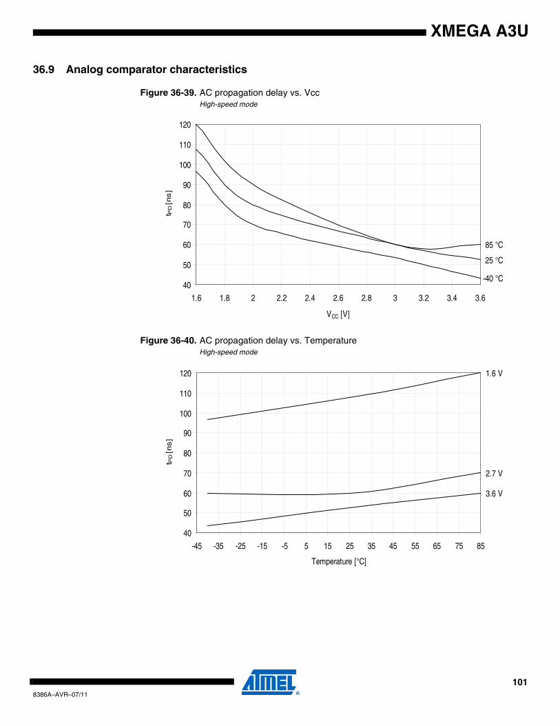
XMEGA A3U
36.9 Analog comparator characteristics
Figure 36-39. AC propagation delay vs. VccHigh-speed mode
Figure 36-40. AC propagation delay vs. TemperatureHigh-speed mode
85 °C
25 °C
-40 °C40
50
60
70
80
90
100
110
120
1.6 1.8 2 2.2 2.4 2.6 2.8 3 3.2 3.4 3.6
VCC [V]
t PD
[ns]
3.6 V
2.7 V
1.6 V
40
50
60
70
80
90
100
110
120
-45 -35 -25 -15 -5 5 15 25 35 45 55 65 75 85
Temperature [°C]
t PD
[ns]
1018386A–AVR–07/11
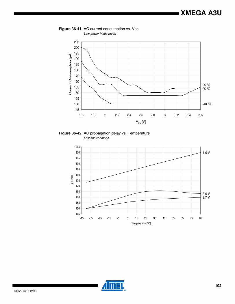
XMEGA A3U
Figure 36-41. AC current consumption vs. VccLow-power Mode mode
Figure 36-42. AC propagation delay vs. TemperatureLow-spower mode
85 °C25 °C
-40 °C
145
150
155
160
165
170
175
180
185
190
195
200
205
1.6 1.8 2 2.2 2.4 2.6 2.8 3 3.2 3.4 3.6
VCC [V]
Cu
rre
nt
Co
nsu
mp
tio
n [
µA
]
3.6 V2.7 V
1.6 V
145
150
155
160
165
170
175
180
185
190
195
200
205
-45 -35 -25 -15 -5 5 15 25 35 45 55 65 75 85
Temperature [°C]
tPD [ns]
1028386A–AVR–07/11
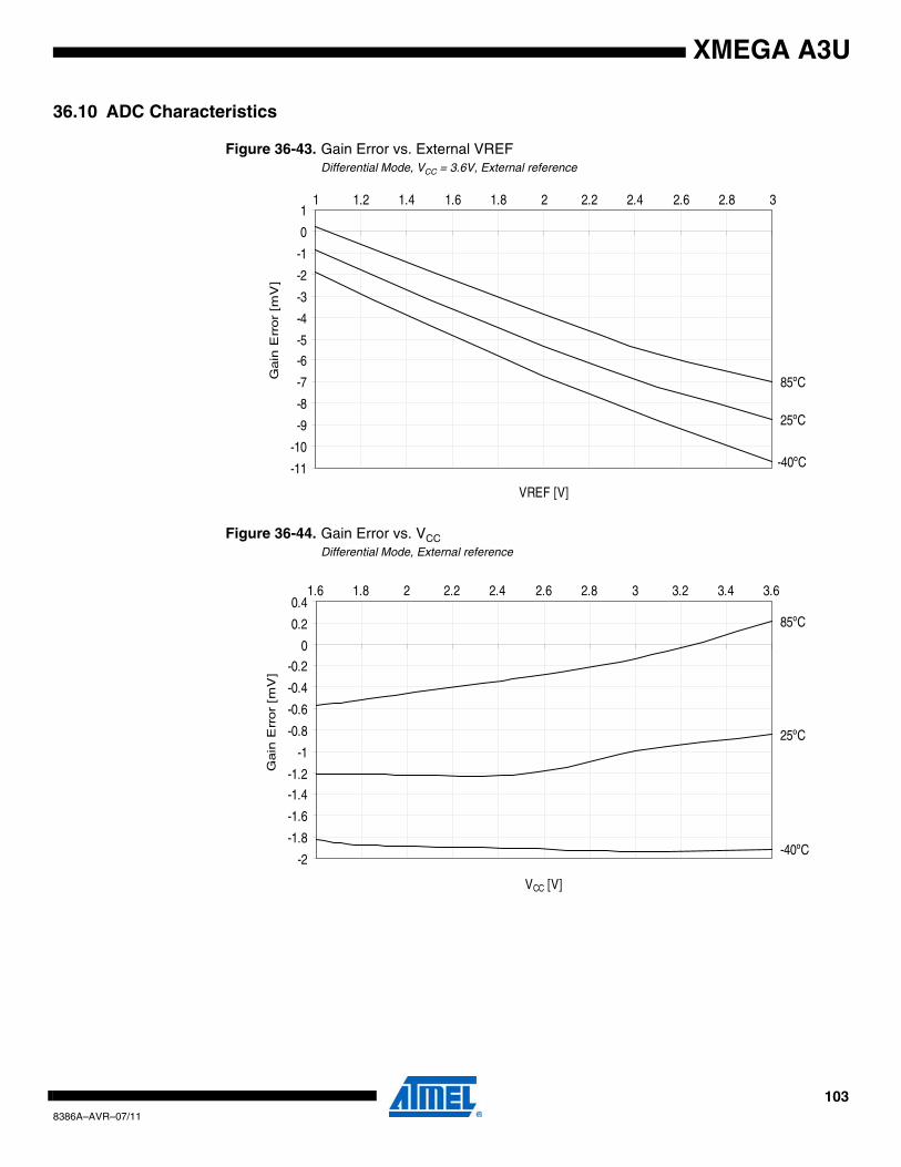
XMEGA A3U
36.10 ADC Characteristics
Figure 36-43. Gain Error vs. External VREFDifferential Mode, VCC = 3.6V, External reference
Figure 36-44. Gain Error vs. VCCDifferential Mode, External reference
85ºC
-40ºC
25ºC
-11
-10
-9
-8
-7
-6
-5
-4
-3
-2
-1
0
11 1.2 1.4 1.6 1.8 2 2.2 2.4 2.6 2.8 3
VREF [V]
Gain
Err
or
[mV
]
85ºC
-40ºC
25ºC
-2
-1.8
-1.6
-1.4
-1.2
-1
-0.8
-0.6
-0.4
-0.2
0
0.2
0.41.6 1.8 2 2.2 2.4 2.6 2.8 3 3.2 3.4 3.6
VCC [V]
Gain
Err
or
[mV
]
1038386A–AVR–07/11
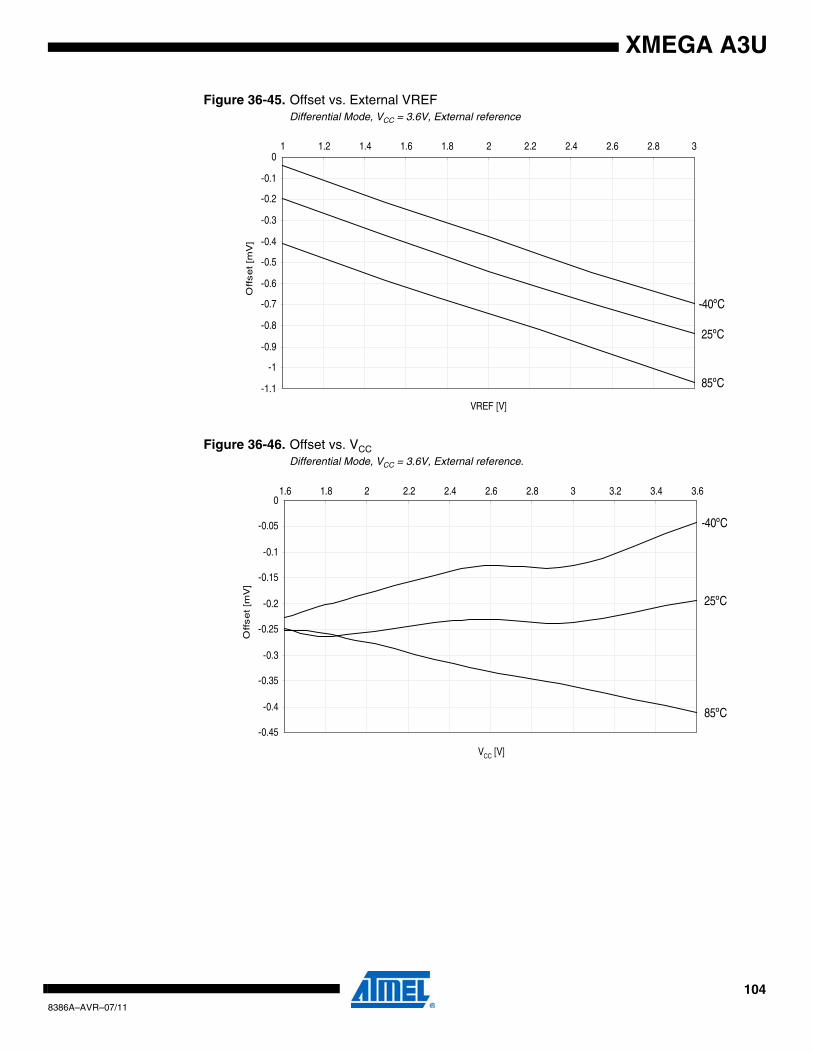
XMEGA A3U
Figure 36-45. Offset vs. External VREFDifferential Mode, VCC = 3.6V, External reference
Figure 36-46. Offset vs. VCCDifferential Mode, VCC = 3.6V, External reference.
85ºC
-40ºC
25ºC
-1.1
-1
-0.9
-0.8
-0.7
-0.6
-0.5
-0.4
-0.3
-0.2
-0.1
01 1.2 1.4 1.6 1.8 2 2.2 2.4 2.6 2.8 3
VREF [V]
Offset [m
V]
85ºC
-40ºC
25ºC
-0.45
-0.4
-0.35
-0.3
-0.25
-0.2
-0.15
-0.1
-0.05
01.6 1.8 2 2.2 2.4 2.6 2.8 3 3.2 3.4 3.6
VCC [V]
Offset [m
V]
1048386A–AVR–07/11
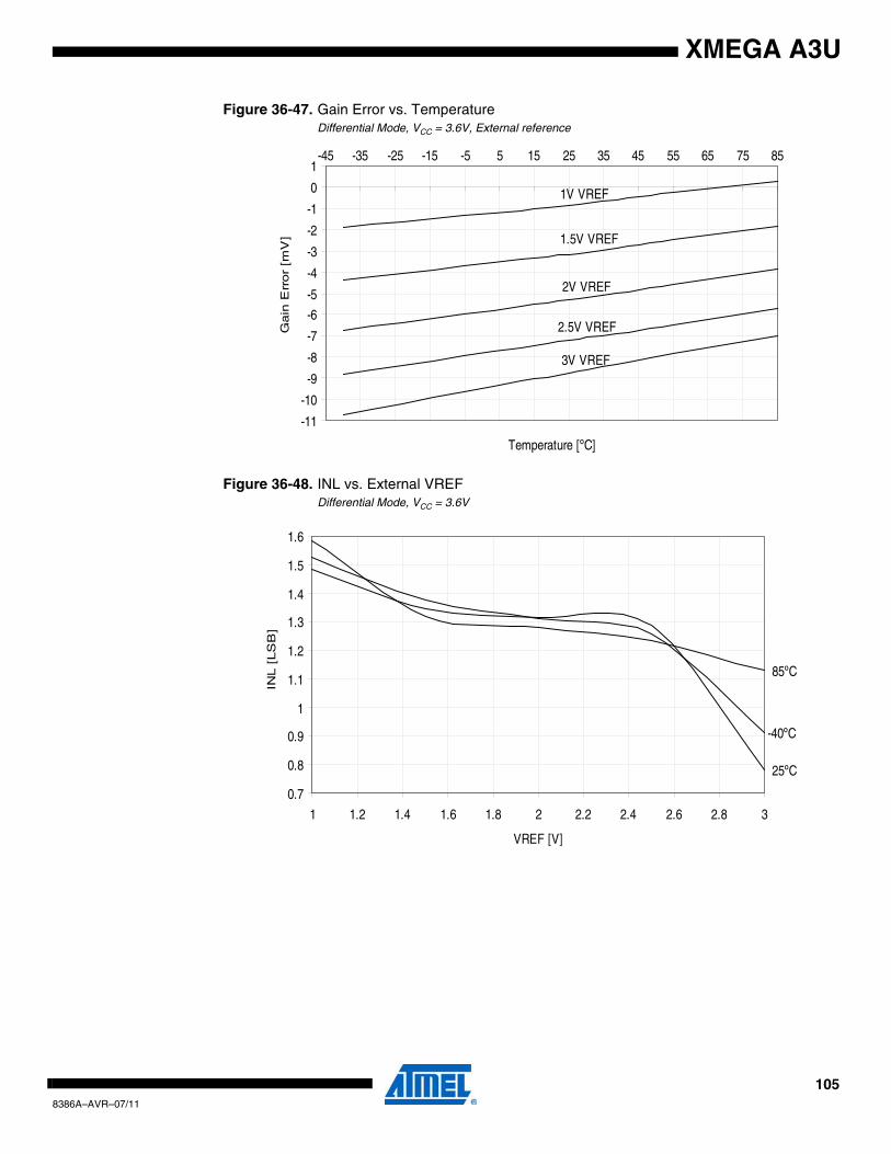
XMEGA A3U
Figure 36-47. Gain Error vs. TemperatureDifferential Mode, VCC = 3.6V, External reference
Figure 36-48. INL vs. External VREFDifferential Mode, VCC = 3.6V
3V VREF
2V VREF
2.5V VREF
1V VREF
1.5V VREF
-11
-10
-9
-8
-7
-6
-5
-4
-3
-2
-1
0
1-45 -35 -25 -15 -5 5 15 25 35 45 55 65 75 85
Temperature [ºC]
Gain
Err
or
[mV
]
85ºC
-40ºC
25ºC
0.7
0.8
0.9
1
1.1
1.2
1.3
1.4
1.5
1.6
1 1.2 1.4 1.6 1.8 2 2.2 2.4 2.6 2.8 3
VREF [V]
INL [
LS
B]
1058386A–AVR–07/11
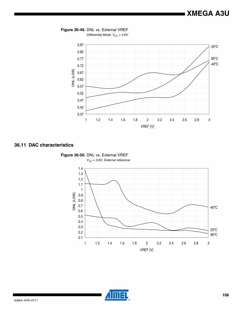
XMEGA A3U
Figure 36-49. DNL vs. External VREFDifferential Mode, VCC = 3.6V
36.11 DAC characteristics
Figure 36-50. DNL vs. External VREFVCC = 3.6V, External reference
85ºC
-40ºC
25ºC
0.37
0.42
0.47
0.52
0.57
0.62
0.67
0.72
0.77
0.82
0.87
1 1.2 1.4 1.6 1.8 2 2.2 2.4 2.6 2.8 3
VREF [V]
DN
L [
LS
B]
85ºC
-40ºC
25ºC
0.10.2
0.30.40.5
0.60.70.80.9
11.11.2
1.31.4
1 1.2 1.4 1.6 1.8 2 2.2 2.4 2.6 2.8 3
VREF [V]
DN
L [
LS
B]
1068386A–AVR–07/11
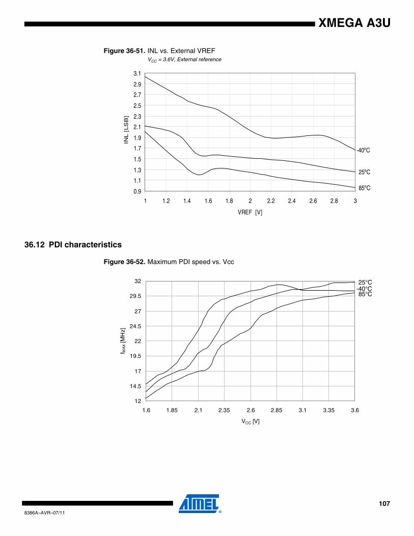
XMEGA A3U
Figure 36-51. INL vs. External VREFVCC = 3.6V, External reference
36.12 PDI characteristics
Figure 36-52. Maximum PDI speed vs. Vcc
85ºC
-40ºC
25ºC
0.9
1.1
1.3
1.5
1.7
1.9
2.1
2.3
2.5
2.7
2.9
3.1
1 1.2 1.4 1.6 1.8 2 2.2 2.4 2.6 2.8 3
VREF [V]
INL [
LS
B]
85°C
25°C-40°C
12
14.5
17
19.5
22
24.5
27
29.5
32
1.6 1.85 2.1 2.35 2.6 2.85 3.1 3.35 3.6
VCC [V]
f MA
X [M
Hz]
1078386A–AVR–07/11
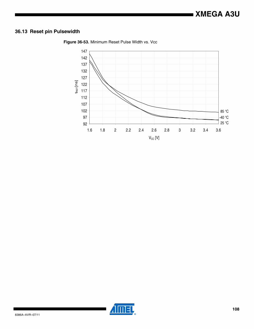
XMEGA A3U
36.13 Reset pin Pulsewidth
Figure 36-53. Minimum Reset Pulse Width vs. Vcc
85 °C
25 °C-40 °C
92
97
102
107
112
117
122
127
132
137
142
147
1.6 1.8 2 2.2 2.4 2.6 2.8 3 3.2 3.4 3.6
VCC [V]
t RS
T [n
s]
1088386A–AVR–07/11
XMEGA A3U
37. Errata
37.1 ATxmega64A3U, ATxmega128A3U, ATxmega192A3U, ATxmega256A3U
37.1.1 Rev. G
• AWeX fault protection restore is not done correct in Pattern Generation Mode
1. AWeX fault protection restore is not done correctly in Pattern Generation ModeWhen a fault is detected the OUTOVEN register is cleared, and when fault condition iscleared, OUTOVEN is restored according to the corresponding enabled DTI channels. ForCommon Waveform Channel Mode (CWCM), this has no effect as the OUTOVEN is correctafter restoring from fault. For Pattern Generation Mode (PGM), OUTOVEN should insteadhave been restored according to the DTILSBUF register.
Problem fix/WorkaroundFor CWCM no workaround is required.
For PGM in latched mode, disable the DTI channels before returning from the fault condi-tion. Then, set correct OUTOVEN value and enable the DTI channels, before the direction(DIR) register is written to enable the correct outputs again.
For PGM in cycle-by-cycle mode there is no workaround.
37.1.2 Rev. A-F
Not sampled.
1098386A–AVR–07/11
XMEGA A3U
38. Datasheet Revision History
Please note that the referring page numbers in this section are referred to this document. Thereferring revision in this section are referring to the document revision.
38.1 8386A – 07/11
1. Initial revision.
1108386A–AVR–07/11
XMEGA A3U
Table of Contents
Features ..................................................................................................... 1
1 Ordering Information ............................................................................... 2
2 Pinout/Block Diagram .............................................................................. 3
3 Overview ................................................................................................... 4
3.1Block Diagram ...........................................................................................................5
4 Resources ................................................................................................. 6
4.1Recommended reading .............................................................................................6
5 Capacitive touch sensing ........................................................................ 6
6 AVR CPU ................................................................................................... 7
6.1Features ....................................................................................................................7
6.2Overview ...................................................................................................................7
6.3ALU - Arithmetic Logic Unit .......................................................................................8
6.4Program Flow ............................................................................................................8
6.5Register File ..............................................................................................................8
7 Memories .................................................................................................. 9
7.1Features ....................................................................................................................9
7.2Overview ...................................................................................................................9
7.3Flash Program Memory ...........................................................................................10
7.4Data Memory ...........................................................................................................11
7.5Production Signature Row .......................................................................................13
7.6User Signature Row ................................................................................................13
7.7Flash and EEPROM Page Size ...............................................................................14
8 DMAC - Direct Memory Access Controller .......................................... 15
8.1Features ..................................................................................................................15
8.2Overview .................................................................................................................15
9 Event System ......................................................................................... 16
9.1Features ..................................................................................................................16
9.2Overview .................................................................................................................16
10 System Clock and Clock options ......................................................... 18
10.1Features ................................................................................................................18
10.2Overview ...............................................................................................................18
i8386A–AVR–07/11

XMEGA A3U
10.3Clock Options ........................................................................................................19
11 Power Management and Sleep Modes ................................................. 21
11.1Features ................................................................................................................21
11.2Overview ...............................................................................................................21
11.3Sleep Modes .........................................................................................................21
12 System Control and Reset .................................................................... 23
12.1Features ................................................................................................................23
12.2Overview ...............................................................................................................23
12.3Reset Sources .......................................................................................................23
13 WDT - Watchdog Timer ......................................................................... 25
13.1Features ................................................................................................................25
13.2Overview ...............................................................................................................25
14 Interrupts and Programmable Multi-level Interrupt Controller .......... 26
14.1Features ................................................................................................................26
14.2Overview ...............................................................................................................26
14.3Interrupt vectors ....................................................................................................26
15 I/O Ports .................................................................................................. 28
15.1Features ................................................................................................................28
15.2Overview ...............................................................................................................28
15.3Output Driver .........................................................................................................29
15.4Input sensing .........................................................................................................31
15.5Alternate Port Functions ........................................................................................31
16 T/C - 16-bit Timer/Counter ..................................................................... 32
16.1Features ................................................................................................................32
16.2Overview ...............................................................................................................32
17 AWeX - Advanced Waveform Extension .............................................. 34
17.1Features ................................................................................................................34
17.2Overview ...............................................................................................................34
18 Hi-Res - High Resolution Extension ..................................................... 35
18.1Features ................................................................................................................35
18.2Overview ...............................................................................................................35
19 RTC - 16-bit Real-Time Counter ............................................................ 36
19.1Features ................................................................................................................36
ii8386A–AVR–07/11
XMEGA A3U
19.2Overview ...............................................................................................................36
20 USB - Universal Serial Bus Interface ................................................... 37
20.1Features ................................................................................................................37
20.2Overview ...............................................................................................................37
21 TWI - Two Wire Interface ....................................................................... 39
21.1Features ................................................................................................................39
21.2Overview ...............................................................................................................39
22 SPI - Serial Peripheral Interface ............................................................ 40
22.1Features ................................................................................................................40
22.2Overview ...............................................................................................................40
23 USART ..................................................................................................... 41
23.1Features ................................................................................................................41
23.2Overview ...............................................................................................................41
24 IRCOM - IR Communication Module .................................................... 42
24.1Features ................................................................................................................42
24.2Overview ...............................................................................................................42
25 AES and DES Crypto Engine ................................................................ 43
25.1Features ................................................................................................................43
25.2Overview ...............................................................................................................43
26 CRC - Cyclic Redundancy Check Generator ....................................... 44
26.1Features ................................................................................................................44
26.2Overview ...............................................................................................................44
27 ADC - 12-bit Analog to Digital Converter ............................................. 45
27.1Features ................................................................................................................45
27.2Overview ...............................................................................................................45
28 DAC - 12-bit Digital to Analog Converter ............................................. 47
28.1Features ................................................................................................................47
28.2Overview ...............................................................................................................47
29 AC - Analog Comparator ....................................................................... 48
29.1Features ................................................................................................................48
29.2Overview ...............................................................................................................48
30 Programming and Debugging .............................................................. 50
iii8386A–AVR–07/11
XMEGA A3U
30.1Features ................................................................................................................50
30.2Overview ...............................................................................................................50
31 Pinout and Pin Functions ...................................................................... 51
31.1Alternate Pin Function Description ........................................................................51
31.2Alternate Pin Functions .........................................................................................53
32 Peripheral Module Address Map .......................................................... 56
33 Instruction Set Summary ...................................................................... 58
34 Packaging information .......................................................................... 62
34.164A ........................................................................................................................62
34.264M2 .....................................................................................................................63
35 Electrical Characteristics ...................................................................... 64
35.1Absolute Maximum Ratings* .................................................................................64
35.2DC Characteristics ................................................................................................64
35.3Operating Voltage and Frequency ........................................................................66
35.4Wakeup time from sleep ........................................................................................67
35.5I/O Pin Characteristics ...........................................................................................68
35.6ADC Characteristics .............................................................................................69
35.7DAC Characteristics .............................................................................................71
35.8Analog Comparator Characteristics .......................................................................72
35.9Bandgap and Internal 1.0V Reference Characteristics .........................................72
35.10Brownout Detection Characteristics ....................................................................73
35.11External Reset Characteristics ............................................................................73
35.12Power-on Reset Characteristics ..........................................................................73
35.13Flash and EEPROM Memory Characteristics .....................................................74
35.14Clock and Oscillator Characteristics ....................................................................74
35.15SPI Characteristics ..............................................................................................78
35.16Two-Wire Interface Characteristics .....................................................................80
36 Typical Characteristics .......................................................................... 82
36.1Active Supply Current ............................................................................................82
36.2Idle Supply Current ................................................................................................84
36.3Power-down Supply Current .................................................................................86
36.4Pin Pull-up .............................................................................................................87
36.5Pin Output Voltage vs. Sink/Source Current .........................................................89
36.6Pin Thresholds and Hysteresis ..............................................................................93
iv8386A–AVR–07/11
36.7Bod Characteristics ...............................................................................................95
36.8Oscillators ..............................................................................................................96
36.9Analog comparator characteristics ......................................................................101
36.10ADC Characteristics ..........................................................................................103
36.11DAC characteristics ...........................................................................................106
36.12PDI characteristics ............................................................................................107
36.13Reset pin Pulsewidth .........................................................................................108
37 Errata ..................................................................................................... 109
37.1ATxmega64A3U, ATxmega128A3U, ATxmega192A3U, ATxmega256A3U .......109
38 Datasheet Revision History ................................................................ 110
38.18386A – 07/11 .....................................................................................................110
Table of Contents....................................................................................... i

Atmel Corporation2325 Orchard ParkwaySan Jose, CA 95131USATel: (+1)(408) 441-0311Fax: (+1)(408) 487-2600 www.atmel.com
Atmel Asia LimitedUnit 1-5 & 16, 19/FBEA Tower, Millennium City 5418 Kwun Tong RoadKwun Tong, KowloonHONG KONGTel: (+852) 2245-6100Fax: (+852) 2722-1369
Atmel Munich GmbHBusiness CampusParkring 4D-85748 Garching b. MunichGERMANYTel: (+49) 89-31970-0Fax: (+49) 89-3194621
Atmel Japan9F, Tonetsu Shinkawa Bldg.1-24-8 ShinkawaChuo-ku, Tokyo 104-0033JAPANTel: (+81)(3) 3523-3551Fax: (+81)(3) 3523-7581
© 2011 Atmel Corporation. All rights reserved.
Atmel®, Atmel logo and combinations thereof, AVR®, QTouch®, QMatrix®, AVR Studio® and others are registered trademarks or trade-marks of Atmel Corporation or its subsidiaries. Windows® and others are registered trademarks of Microsoft Corporation in U.S. and other countries. Other terms and product names may be trademarks of others.
Disclaimer: The information in this document is provided in connection with Atmel products. No license, express or implied, by estoppel or otherwise, to any intellectual property right is granted by this document or in connection with the sale of Atmel products. EXCEPT AS SET FORTH IN THE ATMEL TERMS AND CONDITIONS OF SALES LOCATED ON THE ATMEL WEBSITE, ATMEL ASSUMES NO LIABILITY WHATSOEVER AND DISCLAIMS ANY EXPRESS, IMPLIED OR STATUTORY WARRANTY RELATING TO ITS PRODUCTS INCLUDING, BUT NOT LIMITED TO, THE IMPLIED WARRANTY OF MERCHANTABILITY, FITNESS FOR A PARTICULAR PURPOSE, OR NON-INFRINGEMENT. IN NO EVENT SHALL ATMEL BE LIABLE FOR ANY DIRECT, INDIRECT, CONSEQUENTIAL, PUNITIVE, SPECIAL OR INCIDENTAL DAMAGES (INCLUDING, WITHOUT LIMITATION, DAMAGES FOR LOSS AND PROF-ITS, BUSINESS INTERRUPTION, OR LOSS OF INFORMATION) ARISING OUT OF THE USE OR INABILITY TO USE THIS DOCUMENT, EVEN IF ATMEL HAS BEEN ADVISED OF THE POSSIBILITY OF SUCH DAMAGES. Atmel makes no representations or warranties with respect to the accuracy or com-pleteness of the contents of this document and reserves the right to make changes to specifications and product descriptions at any time without notice. Atmel does not make any commitment to update the information contained herein. Unless specifically provided otherwise, Atmel products are not suit-able for, and shall not be used in, automotive applications. Atmel products are not intended, authorized, or warranted for use as components in applica-tions intended to support or sustain life.
8386A–AVR–07/11