avogadro-scale engineering: form and function mit, november 18, 19 2003 1 three dimensional...
TRANSCRIPT

1Avogadro-Scale Engineering: Form and FunctionMIT, November 18, 19 2003
Three Dimensional Integrated Circuits
C.S. Tan, A. Fan, K.N. Chen, S. Das, N. Checka and R. Reif
Microsystems Technology Laboratories
M.I.T.

2Avogadro-Scale Engineering: Form and FunctionMIT, November 18, 19 2003
3-D Integrated Circuits (3-D IC)
A vertical stack of multiple device and interconnect layers connected together by interlayer vertical vias.
Device/Interconnect Layer
Interlayer Vertical Via

3Avogadro-Scale Engineering: Form and FunctionMIT, November 18, 19 2003
3-D IC with Cu-Cu Wafer Bonding
(R. Reif, MIT)
Interlayer Vertical Via
Cu-Cu Bonding
M3M2M1
M3M2M1
M4
DL2
DL1
DL – Device Layer
M – Metal Interconnect Layer

4Avogadro-Scale Engineering: Form and FunctionMIT, November 18, 19 2003
How Does 3-D Integration Help?
• Greater number of nearest neighbors for a given transistor
• Every transistor, gate, and module has increased wiring bandwidth
• Interconnect distribution becomes shifted– Fewer global wires, more
local wires• Energy consumption and cycle
time reduced• More effective use of Si area
Wire-lengthN
um
ber
of
Inte
r co
nn
ects
(Log-Log Plot)
2-D IC3-D IC

5Avogadro-Scale Engineering: Form and FunctionMIT, November 18, 19 2003
Digital Block Partitioning
2D
Logic
Memory
d
w
L
3D
Logic
Memory
<d
<w
<<L
–Exploit locality to reduce interconnect lengths–Reduce chip area for interconnect-dominated applications–Increase density for device-dominated applications

6Avogadro-Scale Engineering: Form and FunctionMIT, November 18, 19 2003
Mixed-Signal Partitioning
Digital Analog
2D 3D
Digital
Analog
–Mixed-technology/mixed-signal based applications–Better signal isolation between analog and digital components

7Avogadro-Scale Engineering: Form and FunctionMIT, November 18, 19 2003
Monolithic integration of different dies
Board
uP
Memory
DSP
RF
3D2D
Microprocessor Memory
DSP RF
Board
-Smaller form factor-Reduced power dissipation and/or energy consumption

8Avogadro-Scale Engineering: Form and FunctionMIT, November 18, 19 2003
3-D Approaches
• Parallel fabrication, layer transfer by bonding
- Dielectric : polymer, SiO2
- Metallic : Cu-Cu
• Continuous layer growth/fabrication

9Avogadro-Scale Engineering: Form and FunctionMIT, November 18, 19 2003
Cu-Cu Wafer Bonding
(R. Reif, MIT)
Interlayer Vertical Via
Cu-Cu Bonding
M3M2M1
M3M2M1
M4
DL2
DL1
DL – Device Layer
M – Metal Interconnect Layer

10Avogadro-Scale Engineering: Form and FunctionMIT, November 18, 19 2003
Crystallization of -Si
Bulk Si
n+/p+
n+/p+ n+/p+
Gate
Gate
T1
T2
M1
M2
M3
M4
n+/p+n+/p+
Gate
n+/p+
M’1
M’2
VILIC
Via
Memory orAnalog
Recrystallized Si
Logic
Repeaters or optical I/O devices
(K.Saraswat, Stanford)

11Avogadro-Scale Engineering: Form and FunctionMIT, November 18, 19 2003
3-D Research @ MIT
• Process Technology Development
• CAD Tool Development
• Applications: 3-D Circuit/System
- Partitioning Digital Circuits
- Partitioning Mixed-Signal Circuits
- Monolithically integrating several dies

12Avogadro-Scale Engineering: Form and FunctionMIT, November 18, 19 2003
Process Technology Development

13Avogadro-Scale Engineering: Form and FunctionMIT, November 18, 19 2003
BOX
M1 (Al)
M1 (Al)
LOCOS/STI
LOCOS/STI
Cu Via
Cu Pad
Parallel FEOL Processes on 2 Device Wafers
Device/Interconnect Layer 2 (SOI)
Device/Interconnect Layer 1 (Bulk Si)

14Avogadro-Scale Engineering: Form and FunctionMIT, November 18, 19 2003
•Handle wafer provides mechanical support and ease of wafer handling
• Strong enough to withstand subsequent process
• Ease of release
SOI Wafer is attached to a handle wafer
SOI Wafer Thinning
•SOI wafer etch back
• A combination of mechanical grinding, plasma dry etch and chemical wet etch
• Advantage of SOI – Etch stop on BOX
Cu Via and Pad formation
•Via etch, passivation, barrier layer and fill
• Cu Pad for bonding
Precision alignment and bonding

15Avogadro-Scale Engineering: Form and FunctionMIT, November 18, 19 2003
• Optical alignment
• Back-to-face bonding
• Cu to Cu Bonding
• Via pad is for electrical connection
• Dummy pad is to increase bonding strength
Precision alignment and bonding
Handle Wafer Release
• Fast process is required to minimize damage to the stack
16Avogadro-Scale Engineering: Form and FunctionMIT, November 18, 19 2003
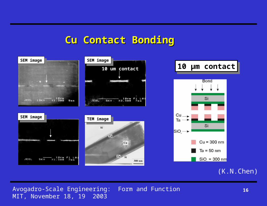
Cu Contact BondingCu Contact Bonding
10 µm contact10 µm contact10 um contactSEM imageSEM image
TEM imageTEM imageSEM imageSEM image
SEM imageSEM image
(K.N.Chen)

17Avogadro-Scale Engineering: Form and FunctionMIT, November 18, 19 2003
CAD Tool Development

18Avogadro-Scale Engineering: Form and FunctionMIT, November 18, 19 2003
FFT – Energy Consumption
• 27% - 40% reduction in switching energy
• Can obtain almost all the energy savings while maintaining cycle time

19Avogadro-Scale Engineering: Form and FunctionMIT, November 18, 19 2003
Future
• Introduce nanotubes/nanowires– Develop active/passive interconnects (wires
that process and/or transmit information)
– Develop insulators with high thermal conductivities (thermal profiles)
– Develop nano-inductors (RF applications)