automotive headlamp hid ballast using a dspic® digital...
TRANSCRIPT
AN1372Automotive Headlamp HID Ballast Reference Design
Using the dsPIC® DSC Device
INTRODUCTIONIn recent years, High Intensity Discharge (HID) lampshave been accepted as a good lighting source forautomotive headlight applications. However, the start-up process of an automotive HID lamp is complex. Itconsists of six stages and each stage presents differentcharacteristics, which need different control strategies.
A digitally controlled ballast has many advantages overthe traditional analog approach:
• Convenient implementation of sophisticated control algorithms
• High performance operation• Effective protection• Very robust• Low cost
This application note focuses on the implementation ofan automotive HID electronic ballast using a MicrochipGS-series 16-bit Digital Signal Controller (DSC).
HID LampGas is a good insulator under normal conditions.However, special conditions such as a strong electricfield, x-ray radiation, ion bombardment, and hightemperature heat could lead to ionization of gasmolecules and produce free-charged particles. Thesecharged particles can conduct current under an electricfield, which is known as gas discharge.
The light source made by this principle is called a gasdischarge lamp. A HID lamp is one kind of gasdischarge lamp. Others include high-pressure mercurylamps, high-pressure sodium lamps, metal halidelamps and some rare gas lamps, such as Xenon andKrypton lamps.
HID lamps have many advantages over incandescentand fluorescent lighting, such as long lamp life, highefficiency, high brightness and low power consumption.They are widely used in factory buildings, airports,stadiums and square-shaped lighting fixtures. Inaddition, Xenon lamps are widely used in automotiveapplications.
Compared with conventional halogen lamps, Xenonlamps have features of high luminous efficacy, lowpower consumption, good color rendering and longlamp life. Xenon lamp automotive headlamp systemsgreatly improve the safety of driving at night.
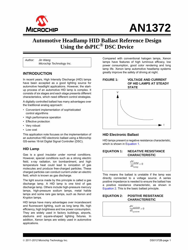
FIGURE 1: VOLTAGE AND CURRENT OF HID LAMPS AT STEADY STATE
HID Electronic BallastHID lamps present a negative resistance characteristic,which is shown in Equation 1.
EQUATION 1: NEGATIVE RESISTANCE CHARACTERISTIC
This means the ballast is unstable if the lamp wasdirectly connected to a voltage source. A seriespositive impedance is needed to ensure the ballast hasa positive resistance characteristic, as shown inEquation 2. This is the basic ballast principle.
EQUATION 2: POSITIVE RESISTANCE CHARACTERISTIC
Author: Jin WangMicrochip Technology Inc.
I
V
dVlampdIlamp----------------- 0<
dVsystemdIsystem--------------------- 0>
© 2011-2012 Microchip Technology Inc. DS01372B-page 1

AN1372
A traditional inductive ballast shown in Figure 2 hasmany problems such as large bulk capacitors, lowPower Factor (PF) and difficulty reigniting. Anelectronic ballast is used to control the lamp currentand lamp output power. Instant start-up, small size,high PF, and high efficiency can be achieved using anelectronic ballast.FIGURE 2: INDUCTIVE BALLAST
Good electronic ballasts must have the followingimportant features:
• High power factor, greater than 0.9 at the ballast input
• THD should be limited below 33%• No flicker during the lamp start-up process • High power efficiency• No acoustic resonance
Technical Background of Automotive HID BallastThe start-up process of automotive HID lamps is quitecomplex. Figure 3 shows the working profile of HIDlamp voltage and current during the start-up process.This is the inherent characteristic of an HID lamp andthe ballast must be designed to meet this profile;otherwise, the HID lamp will not operate as expected.
FIGURE 3: AUTOMOTIVE HID LAMP VOLTAGE AND CURRENT(1)
L
AC INC
Lamp
Vlamp(2)
Ilamp
Turn-onIgnitio
nTakeover
Warm-up
Run-upSteady-state
30 ms 50 ms 6s-8s
-400V
25 kV
20V-40V20V-65V
65V-105V
0A
-12Amax -2.5A (max)
2.5A~0.41A0.41A (@85V,35W)
2.5A(max)
• Turn-on: Before ignition, the lamp’s equivalent impedance is considered as infinite, so the ballast is treated as an open circuit. In this stage, the ballast produces adequate voltage. In this stage, the voltage generated by the ballast is fed to the igniter circuitry to ignite the lamp.
• Ignition: Automotive HID lamps are high pressure gas lamps. During this stage, the igniter circuitry generates a high voltage pulse across the lamp and the lamp transfers from isolation status to current conductive status. As the result, an arc is established in the tube and visible light is generated. The required ignition voltage for a hot lamp is around 25 kV. For a cold lamp, the voltage is around 10 kV.
• Takeover: After successful ignition, the lamp requires a large current (takeover current) to sustain the arc. The output capacitance and auxiliary current circuit can provide this high magnitude current before the DC/DC converter delivers enough power to the lamp.
• Warm-up: In this stage, the DC/DC converter provides a certain amount of current, depending on the lamp condition to sustain the arc. The converter works as current mode, and generates a square wave AC current. As the frequency is small (20 Hz) when compared to steady-state, it’s also called DC status.
• Run-up: This is the key stage of the start-up process. In order to meet the SAE J2009 and ECE Reg. No 99 specification for the light output versus time, the start transient power of the lamp is much higher than the steady state. Then, the ballast controls the lamp power to ramp down to the normal level.
• Steady State: The lamp voltage is ~ 85V, and the lamp current is ~0.4A, depending on lamp conditions. But the lamp power is recommended to be 35W, ±1W. This helps to ensure better output light performance and longer lamp life.
Note 1: The data presented in this figure depends on the lamp part number and working conditions.2: Vlamp in the turn-on stage is high-frequency AC; in this instance only its profile is illustrated.
DS01372B-page 2 © 2011-2012 Microchip Technology Inc.

AN1372
The ballast in this reference design consists of foursections, as shown in Figure 4:• High frequency DC/DC converter• Low frequency DC/AC inverter• Ignition circuit• Digital Signal Controller
The DC/DC converter boosts the battery voltage (9V-16V) to a high level for the ignition circuit first, and thendrops to ~85V for steady state operation. The DC/ACinverter converts the DC current to a square wavecurrent to energize the two lamp electrodes equally.The high voltage igniter generates high voltage pulsesto strike the lamp. Both The DC/DC converter and theDC/AC inverter are controlled by a single digital signalcontroller.
FIGURE 4: BLOCK DIAGRAM OF THE DIGITAL REFERENCE DESIGN AUTOMOTIVE HID BALLAST
Lamp
Igniter
DC/ACInverter
Inverter signalDigital Signal Controller
Ilamp
VlampDC/DC
Converter
PWM signal
Bat
tery
© 2011-2012 Microchip Technology Inc. DS01372B-page 3

AN1372
AUTOMOTIVE HID BALLAST DIGITAL DESIGN
System Design SpecificationsTable 1 lists the system specifications used for theautomotive HID ballast digital design.
TABLE 1: SYSTEM DESIGN SPECIFICATIONSCharacteristic Specification Conditions
Input Voltage Nominal 13.5V
—
Operation 9V-16VTemperature Range Operation -40ºC to 105ºCTransient Maximum input current Cold lamp: 12A
Hot lamp: 4A
Maximum output current 2.5AMaximum input power
115W13.5V, 25ºC
9V-16V, -40ºC to 105ºCMaximum output power
75W13.5V, 25ºC9V-16V, -40ºC to 105ºC
Light output Meet ECE R99 13.5V, 25ºCSteady Input current 3.5A maximum 13.5V, -40ºC to 105ºC
Output power 35W ±1W 9V-16V, -40ºC to 105ºCTime of steady light output ≤ 150s 13.5V, 25ºCEfficiency > 85% 13.5V
Acoustic Resonance — No acoustic resonance —Flicker — No flickerReliability Restrike 100% 100 times turn-on/off
Successive operation 3000 hours
—
Input Protection Undervoltage protection 9VOvervoltage protection 16V
Output Protection Short-circuit protection YesOpen circuit protection Yes
Dimension — ≤10 mm * 60 mm * 80 mmEMI — Meet ECE R10
(error < 20%)
DS01372B-page 4 © 2011-2012 Microchip Technology Inc.
AN1372
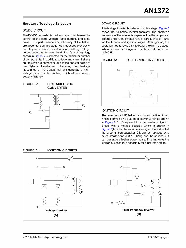
Hardware Topology SelectionDC/DC CIRCUITThe DC/DC converter is the key stage to implement thecontrol of the lamp voltage, lamp current, and lamppower. The performance and efficiency of the ballastare dependent on this stage. As introduced previously,this stage must have a boost function and large voltageoutput capability for open load. The flyback topologyshown in Figure 5 is selected for the minimum numberof components. In addition, voltage and current stresson the switch is decreased due to the boost function ofthe flyback transformer. However, the leakageinductance of the transformer will generate a high-voltage pulse on the switch, which affects systempower efficiency.
FIGURE 5: FLYBACK DC/DC CONVERTER
DC/AC CIRCUITA full-bridge inverter is selected for this stage. Figure 6shows the full-bridge inverter topology. The operationfrequency of the inverter is dependent on the lamp state.Before ignition, the inverter runs at a frequency of 1 kHzfor the turn-on and ignition stages. After ignition, theoperation frequency is only 20 Hz for the warm-up stage.When the warm-up stage is over, the inverter operatesat 200 Hz.
FIGURE 6: FULL-BRIDGE INVERTER
IGNITION CIRCUITThe automotive HID ballast adopts an ignition circuit,which is driven by a dual-frequency inverter, as shownin Figure 7(B). Compared to a conventional ignitioncircuit with a voltage doubler, which is shown inFigure 7(A), it has two main advantages: the first is thatthe large ignition capacitor, C1, can be replaced by amuch smaller one (C3 ≤ C1/10), and the second is itcan generate a higher power pulse. This improves theignition success rate especially for a hot lamp strike.
FIGURE 7: IGNITION CIRCUITS
Vin
Vout
Vdc
Load
C1 C2 C3
C4
Voltage Doubler Dual-frequency Inverter
(A) (B)
© 2011-2012 Microchip Technology Inc. DS01372B-page 5

AN1372
DIGITAL SIGNAL CONTROLLERThe dsPIC DSC detects the lamp voltage and lampcurrent through the Analog-to-Digital Converter(ADC) pair 0 (AN0 and AN1). Then, the currentreference of the DC/DC converter is calculatedaccording to the lamp voltage. The controller adjuststhe PWM duty cycle of the DC/DC converter tocontrol the lamp current. Meanwhile, several faultsignals are monitored by the digital signal controller.Open circuit protection and short circuit protectionneed rapid response, so the internal comparators(CMP1D and CMP2D) are selected to implementthese two protections. At the same time, the digitalsignal controller measures the battery voltagethrough the ADC pair 1 (AN2). If the battery voltageis outside the normal operation range, the ballast willstop working. In addition, Timer2 of the DSC is usedto control the operation frequency of the full-bridgeinverter, and the inverter drive signal is producedthrough the I/O port, RB14.Table 2 shows the dsPIC usage and Table 8 shows theblock diagram of the digital signal controller.
TABLE 2: dsPIC® USAGE
FIGURE 8: BLOCK DIAGRAM OF THE DIGITAL SIGNAL CONTROLLER
Feature Description
System clock Internal FRC Oscillator
Input voltage protection ADC pair 1; Timer2 for trigger
DC/DC Converter control PWM1
Open and short circuit protection
CMP1D; CMP2D
Lamp current and voltage sample
ADC pair 0; PWM1 for trigger
Full-bridge inverter drive signal
Timer2; RB14
Fail ignition protection Timer2
Delay function Timer1
Indication LED RB4
Vlamp
Ilamp
Ierr Iref PI
Timer2
PWM
Vmin < Vin < Vmax
Full-BridgePWM
Vin
PWM1H AN2 AN1 AN0
Fault
RB14
CM
P1D
CM
P2D
Ballast Circuitry
DAC Output
DAC Output
Signal
RB4IndicationLED
DS01372B-page 6 © 2011-2012 Microchip Technology Inc.

AN1372
Control Strategy and Control Loop DesignCONTROL STRATEGY DESIGNAs introduced in the section “Technical Backgroundof Automotive HID Ballast”, the start-up process ofthe automotive HID lamps consists of six stages. Itneeds different control strategies in every stage andthe timing control is very strict. Figure 9 shows thetiming flowchart of the control strategies.
At the turn-on stage, the ballast should boost thebattery voltage to a proper level. This voltage ismaintained for a period of time to fully charge the ignitercapacitor, until the lamp gas switches from isolation tocurrent conductive state. The DC/DC stage works inconstant voltage control in this mode, as shown inFigure 10(A). Immediately after successful ignition
(lamp gas switches from isolation to current conductivestate), the ballast should respond quickly and providesufficient current to maintain the arc. Constant voltagecontrol is replaced by constant current control at thewarm-up stage, as shown in Figure 10(B). Finally, atthe run-up stage and steady state, the ballast works inpower control mode. When the lamp voltage exceeds30V, it enters into the run-up stage. The ballast shouldcontrol the lamp power from a high level (~75W,depending on the lamp status) to a low level (35W) untilsteady state. During this stage the decreasing powercontrol mode is selected. When the lamp voltageexceeds 65V, the lamp enters into a steady state. Theballast operates at constant power control to maintainthe lamp power at 35W, ±1W. The steady stateschematic is illustrated in Figure 10(C).
FIGURE 9: TIMING FLOWCHART OF THE CONTROL STRATEGIES
FIGURE 10: VOLTAGE, CURRENT AND POWER CONTROL DIAGRAMS (A, B, AND C)
t
Vlamp
Steady
State
Run-up
Warm-up
Take
over
Ignitio
n
Turn-
on
Consta
nt
Voltag
e
Contro
l No
Contro
l No
Contro
lCon
stant
Curren
t
Contro
l
Decrea
sing P
ower
Contro
l
Consta
nt Pow
er
Contro
l
Note: This figure shows the “as is” magnitude profile of the lamp. Its direction is not illustrated here.
Co
ko Gi
K1
Vlamp
Vref
Verr
Co
ko Gi
K2Ilamp
Iref
Ierr
Co
ko Gi
K1
Plamp
Pref
Perr
K2MULT
Constant Voltage Constant Current
Power Control Mode
(A) (B)
(C)
Control ModeControl Mode
© 2011-2012 Microchip Technology Inc. DS01372B-page 7

AN1372
Three different control modes (voltage, current, andpower) are needed during the start-up process, whichmakes the software quite complex. However, thefeatures of the dsPIC DSC minimize the complexity ofthe software design. For example:• Interrupt driven control with multiple priorities• Intelligent peripherals to minimize software
overhead• High performance math and DSP engine to
efficiently perform complex calculations• Built-in comparators to provide high-speed,
reliable protection• Simultaneous sampling ADC for accurate power
measurements
In addition, there are two transitions between twocontrol mode changes in the process. The firsttransition is between the voltage control mode andcurrent control mode. This may delay the currentresponse of the DC/DC converter after ignition, whichmay lead to the lamp arc becoming extinguished. Thesecond transition is between the current control modeand power control mode, which will lead to instability ofthe lamp current. Considering this, the control mode isoptimized in this reference design. Only current controlmode is employed for the entire start-up process. Anadvanced scheme is implemented using the dsPICDSC, which achieves the various control modeswithout the drawbacks of unstable lamp current orextinguishing of the ignition arc.
First, the constant voltage control mode in the turn-onstage is replaced by the constant current control mode.The maximum output voltage of the DC/DC converteris limited by the cycle-by-cycle Current-Limit function ofthe digital signal controller’s PWM module. The limitedvoltage value should be set for the ignition circuit(somewhere between 360V to 400V for igniter circuitrycomponents tolerance). This accelerates the currentresponse of the DC/DC converter, and contributes to ahigh ignition success rate. Also, the takeover currentsupplied by the auxiliary current circuit is reduced;therefore, the auxiliary current capacitor can be asmaller one.
Next, the power control mode is replaced by the currentcontrol mode in the run-up stage and steady state.When the start-up process enters into the run-up stagefrom the warm-up stage, there is no control modetransition, which may lead to instability of the lampcurrent. In this way, we can control the lamp current toachieve lamp power control. The current reference inthese two stages is calculated, as shown in Equation 3.
EQUATION 3: CURRENT REFERENCE FORMULA
During these two stages (Run-up and Steady), thepower reference is determined by lamp voltagesampled by the digital signal controller’s ADC module.The relationship between the power reference andlamp voltage is shown in Figure 11.
FIGURE 11: POWER REFERENCE AND LAMP VOLTAGE
As discussed previously, the current reference of theregulator during the entire start-up process is shown inFigure 12.
Where:Iref is the lamp current referencePref is the lamp power referenceVlamp is the lamp voltage
IrefPref
Vlamp--------------=
Where:Pref is the lamp power referenceVlamp is the lamp voltage
30V 65V Vlamp
Pref
58W
35W
DS01372B-page 8 © 2011-2012 Microchip Technology Inc.
AN1372
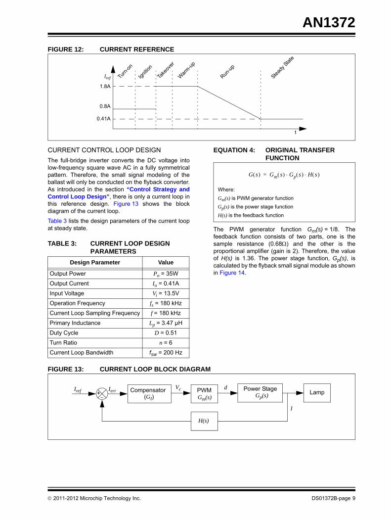
FIGURE 12: CURRENT REFERENCECURRENT CONTROL LOOP DESIGNThe full-bridge inverter converts the DC voltage intolow-frequency square wave AC in a fully symmetricalpattern. Therefore, the small signal modeling of theballast will only be conducted on the flyback converter.As introduced in the section “Control Strategy andControl Loop Design”, there is only a current loop inthis reference design. Figure 13 shows the blockdiagram of the current loop.
Table 3 lists the design parameters of the current loopat steady state.
TABLE 3: CURRENT LOOP DESIGN PARAMETERS
EQUATION 4: ORIGINAL TRANSFER FUNCTION
The PWM generator function Gm(s) = 1/8. Thefeedback function consists of two parts, one is thesample resistance (0.68Ω) and the other is theproportional amplifier (gain is 2). Therefore, the valueof H(s) is 1.36. The power stage function, Gp(s), iscalculated by the flyback small signal module as shownin Figure 14.
FIGURE 13: CURRENT LOOP BLOCK DIAGRAM
Steady
State
Run-up
Warm-up
Take
over
Ignitio
n
Turn-
on
Iref
1.8A
0.8A
0.41A
t
Design Parameter Value
Output Power Po = 35W
Output Current Io = 0.41A
Input Voltage Vi = 13.5V
Operation Frequency fs = 180 kHz
Current Loop Sampling Frequency f = 180 kHz
Primary Inductance Lp = 3.47 µH
Duty Cycle D = 0.51
Turn Ratio n = 6
Current Loop Bandwidth fsw = 200 Hz
Where:Gm(s) is PWM generator functionGp(s) is the power stage functionH(s) is the feedback function
G s( ) Gm s( ) Gp s( ) H s( )⋅⋅=
LampPower StagePWM
I
dVc
H(s)
Compensator(GI)
IerrIref + Gp(s)Gm(s)
© 2011-2012 Microchip Technology Inc. DS01372B-page 9

AN1372
FIGURE 14: SMALL SIGNAL MODEL OF THE FLYBACK CONVERTERBased on Figure 14, the power stage function, Gp(s), iscalculated in Equation 5. As a result, the entire originaltransfer function is calculated, as shown in Equation 6.
EQUATION 5: POWER STAGE TRANSFER FUNCTION
EQUATION 6: ENTIRE ORIGINAL TRANSFER FUNCTION
EQUATION 7: CURRENT ERROR COMPENSATOR
Based on Equation 7,
kpi = 0.1162 and kIi = 14.59/Sampling Frequency = 0.00008.
Vg(t)
Ig(t)
Ig d(t)
L
1:D
(Vg+V/n) * d(t)
1-D:n+
–
RC
V(t)
I * d(t)/n
I(t)
Where:Vo = the input voltageD = the duty cycleD' = (1-D)R = the lamp equivalent resistanceLp = the primary inductance
Gp s( ) v t( )R dt⋅-------------
Vg (t)= 0 =
VoR------
D′D------
LpD′ R⋅--------------s–
n2LpCs2 n2LpR
-----------s D′2+ +
---------------------------------------------------------⋅=
G s( ) Gm s( ) Gp s( ) H s( )⋅ ⋅VoR------
D′D------
LpD′ R⋅--------------s–
n2LpCs2 n2LpR
-----------s D′2+ +
--------------------------------------------------------- 1.368
----------⋅ ⋅= =
Where:Gm(s) = PWM module transfer functionH(s) = Feedback circuitry transfer function
The transfer function for the current error compensator is given by:
Where fz = 20 Hz, which is the location of zero for the current PI controller and,
GI s( ) kpikIis
------ kpi1 Tco s⋅+
Tco s⋅------------------------⎝ ⎠
⎛ ⎞=+=
Tco1
2πfz---------- 0.00796==
GI s( )nLpCD′2R2fsw
VoLp------------------------------------ 8
1.36----------
1 Tco s⋅+Tco s⋅
------------------------⎝ ⎠⎛ ⎞⋅ ⋅=
GI s( ) 0.1162 1 0.00796 s⋅+0.00796 s⋅
-----------------------------------⎝ ⎠⎛ ⎞⋅=⇒
GI s( ) 0.1162 14.59s
-------------+=⇒
DS01372B-page 10 © 2011-2012 Microchip Technology Inc.
AN1372
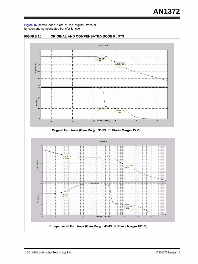
Figure 15 shows bode plots of the original transferfunction and compensated transfer function.FIGURE 15: ORIGINAL AND COMPENSATED BODE PLOTS
Original Functions (Gain Margin 33.83 dB, Phase Margin 15.2º)
Compensated Functions (Gain Margin 48.43dB, Phase Margin 101.7°)
© 2011-2012 Microchip Technology Inc. DS01372B-page 11
AN1372
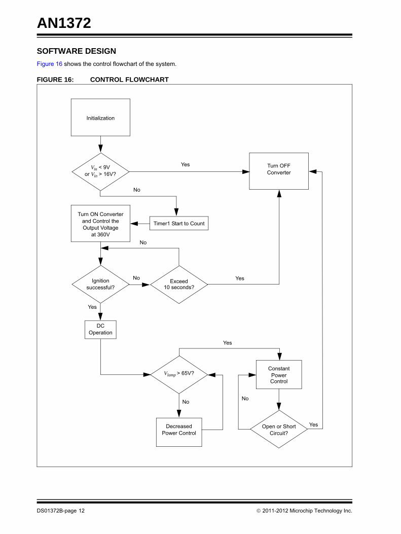
SOFTWARE DESIGNFigure 16 shows the control flowchart of the system.
FIGURE 16: CONTROL FLOWCHART
Initialization
Turn OFFConverter
Timer1 Start to Count
Exceed
Vin < 9Vor Vin > 16V?
Yes
No
No
No
Yes
NoNo
Turn ON Converterand Control theOutput Voltage
at 360V
Ignitionsuccessful?
DCOperation
Vlamp > 65V?Constant
Power
DecreasedPower Control
Open or ShortCircuit?
10 seconds?
Control
Yes
Yes
Yes
DS01372B-page 12 © 2011-2012 Microchip Technology Inc.

AN1372
Timing Logic for Software ImplementationTimer1 runs at a frequency of 1 kHz. It is the time basefor the delay subroutine function, which is used in theignition failure detection. Timer2 is used for the full-bridge inverter drive signal and runs at a differentfrequency.Before ignition, Timer2 runs at a frequency of 2 kHz tocharge the igniter capacitor. After ignition, Timer2 runsat 40 Hz to warm-up the lamp electrode. After thewarm-up stage, Timer2 runs at 400 Hz and remains atthis frequency. In addition, Timer2 triggers ADC pair 1every period to sample the battery voltage.
PWM1 runs at 180 kHz. It also triggers ADC pair 0every eight cycles. Lamp voltage and lamp current aresampled by ADC pair 0. An ADC interrupt is served onevery trigger. In the Interrupt Service Routine (ISR), thedigital signal controller reads the ADC result, checksthe lamp status, executes the compensator, and thenupdates the PWM duty cycle to deliver proper power tothe lamp. The timing diagram is illustrated in Figure 17.
FIGURE 17: TIMING LOGIC
Timer1Counter 1 kHz
Timer2Counter
2 kHz 40 Hz 400 Hz
Trigger
180 kHzPWM1
ADC Pair 1
© 2011-2012 Microchip Technology Inc. DS01372B-page 13
AN1372
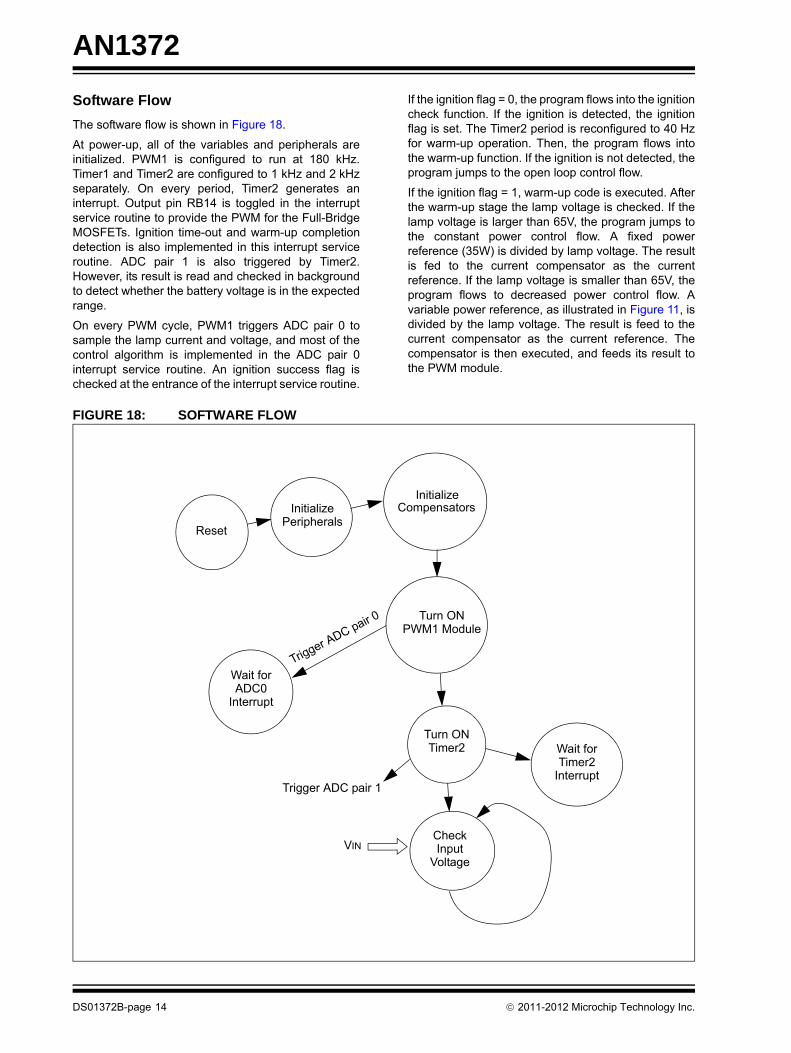
Software FlowThe software flow is shown in Figure 18.At power-up, all of the variables and peripherals areinitialized. PWM1 is configured to run at 180 kHz.Timer1 and Timer2 are configured to 1 kHz and 2 kHzseparately. On every period, Timer2 generates aninterrupt. Output pin RB14 is toggled in the interruptservice routine to provide the PWM for the Full-BridgeMOSFETs. Ignition time-out and warm-up completiondetection is also implemented in this interrupt serviceroutine. ADC pair 1 is also triggered by Timer2.However, its result is read and checked in backgroundto detect whether the battery voltage is in the expectedrange.
On every PWM cycle, PWM1 triggers ADC pair 0 tosample the lamp current and voltage, and most of thecontrol algorithm is implemented in the ADC pair 0interrupt service routine. An ignition success flag ischecked at the entrance of the interrupt service routine.
If the ignition flag = 0, the program flows into the ignitioncheck function. If the ignition is detected, the ignitionflag is set. The Timer2 period is reconfigured to 40 Hzfor warm-up operation. Then, the program flows intothe warm-up function. If the ignition is not detected, theprogram jumps to the open loop control flow.
If the ignition flag = 1, warm-up code is executed. Afterthe warm-up stage the lamp voltage is checked. If thelamp voltage is larger than 65V, the program jumps tothe constant power control flow. A fixed powerreference (35W) is divided by lamp voltage. The resultis fed to the current compensator as the currentreference. If the lamp voltage is smaller than 65V, theprogram flows to decreased power control flow. Avariable power reference, as illustrated in Figure 11, isdivided by the lamp voltage. The result is feed to thecurrent compensator as the current reference. Thecompensator is then executed, and feeds its result tothe PWM module.
FIGURE 18: SOFTWARE FLOW
InitializeCompensators
Turn ONPWM1 Module
Turn ONTimer2 Wait for
Timer2Interrupt
CheckInput
Voltage
Wait forADC0
Interrupt
Reset
InitializePeripherals
Trigger ADC pair 1
VIN
Trigger ADC pair 0
DS01372B-page 14 © 2011-2012 Microchip Technology Inc.

AN1372
FIGURE 19: TIMER2 INTERRUPT SERVICE ROUTINE (ISR) FLOWTimer2Interrupt
ToggleInverterDrive
Check Endof Warm-up
StageCheckIgnitionFailure
Signal
© 2011-2012 Microchip Technology Inc. DS01372B-page 15

AN1372
FIGURE 20: ADC INTERRUPT SERVICE ROUTINE (ISR) FLOWLegend: Text in red indicates labels in the Assembly code.Text in black indicates jump conditions.
ADC0Interrupt Ignition Flag = 1
Startup_Phase_Operation:Ignition Flag = 0Open_Loop:
Open
_Con
trol
:
Confirm_Ignition:
Step
_up:
Decreased_power_control:
Cons
tant
_con
trol
_Ope
rati
on:
De
cr
ea
se
d_
Vo
lt
ag
e_
co
nt
ro
l:
IgnitionCheck
Filter LampCurrent
FeedbackSignal
Filter LampVoltage
FeedbackSignal
CalculateIref
CurrentLoop
Compensator
CurrentLoop
Compensator
Warm-upStage
CurrentCompensator
VoltageLoop
Compensator
UpdateInverter
Frequency
CalculateIref
Bus_
War
mup
_Suc
cess
_Fla
g!=
2 Bus_Warmup_Success_Flag = 2
V lamp
> 65
V
Ilamp > 0.3A
I lam
p <
0.3A
Ilamp
PWM
PWM
PWM
PWM
Vlamp < 65V
Vlamp
Ilamp
Loop
DS01372B-page 16 © 2011-2012 Microchip Technology Inc.
AN1372
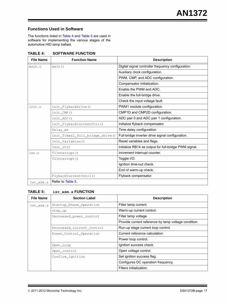
Functions Used in SoftwareThe functions listed in Table 4 and Table 5 are used insoftware for implementing the various stages of theautomotive HID lamp ballast.TABLE 4: SOFTWARE FUNCTION
TABLE 5: isr_asm.s FUNCTION
File Name Function Name Description
main.c main() Digital signal controller frequency configuration.
Auxiliary clock configuration.
PWM, CMP, and ADC configuration.
Compensator initialization.
Enable the PWM and ADC.
Enable the full-bridge drive.
Check the input voltage fault.
init.c init_FlybackDrive() PWM1 module configuration.
init_CMP() CMP1D and CMP2D configuration.
init_ADC() ADC pair 0 and ADC pair 1 configuration.
init_FlybackCurrentCtrl() Initialize flyback compensator.
Delay_ms Time delay configuration.
init_Timer2_full_bridge_drive() Full-bridge inverter drive signal configuration.
Init_Variables() Reset variables and flags.
Init_IO() Initialize RB14 as output for full-bridge PWM signal.
isr.c T1Interrupt() Increment interrupt counter.
T2Interrupt() Toggle I/O.
Ignition time-out check.
End of warm-up check.
FlybackCurrentCntrl() Flyback compensator.
isr_asm.s Refer to Table 5.
File Name Section Label Description
isr_asm.s Startup_Phase_Operation Filter lamp current.
step_up Warm-up current control.
Decreased_power_control Filter lamp voltage.
Provide current reference by lamp voltage condition.
Decreased_current_control Run-up stage current loop control.
Power_Control_Operation Current reference calculation.
Power loop control.
Open_Loop Ignition success check.
Open_control Open voltage control.
Confirm_ignition Set ignition success flag.
Configures DC operation frequency.
Filters initialization.
© 2011-2012 Microchip Technology Inc. DS01372B-page 17

AN1372
HARDWARE DESIGN
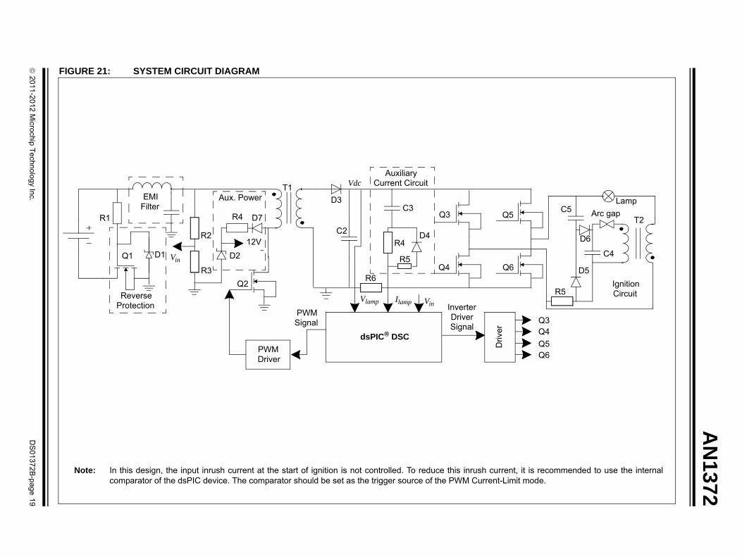
System Block DiagramFigure 21 shows the system circuit diagram of thereference design. As introduced in the section“Hardware Topology Selection”, the design consistsof four major sections. In addition, the design alsoincludes several auxiliary circuits.
An EMI filter at the input side attenuates theElectromagnetic Interference (EMI). At the same time,a reverse input-voltage protection circuit is also at theinput side. Moreover, an RCD auxiliary current circuitbefore the full-bridge inverter provides the major take-over current before the response of the converter. Asignal filter adjusts the lamp voltage and current signalsbefore the ADC. Finally, the auxiliary power systemsupplies the digital and analog ICs on the board.
Power Stage Parameter Design
TABLE 6: FLYBACK DESIGN DATADesign Parameter Value
Rated input voltage Vin = 13.5V
Minimum input voltage Vin_min = 9V
Maximum input voltage Vin_max = 16V
Rated output voltage Vo = 85V
Minimum output voltage Vo_min = 30V
Maximum output voltage Vo_max = 102V
Rated output current Io = 0.41A
Maximum output current Io_max = 1.8A
Rated output power Po = 35W
Maximum output power Po_max = 75W
Operation frequency fs = 180 kHz
System efficiency η = 85%
Diode forward voltage Vf = 1V
DS01372B-page 18 © 2011-2012 Microchip Technology Inc.
© 2011-2012 M
icrochip Technology Inc.D
S01372B
-page 19
AN
1372F
T2
LampArc gapC5
C4
D5
R5IgnitionCircuit
, it is recommended to use the internalit mode.
Q3Q4Q5Q6
D6
IGURE 21: SYSTEM CIRCUIT DIAGRAM
R1
EMIFilter
D7R4
T1D3
C2
Q1
Q2
C3
R4D4
Q3 Q5
Q4 Q6
dsPIC® DSC
Vdc
D1
R2
R3Vin R5
IlampVlamp
R6
Vin
AuxiliaryCurrent Circuit
PWM Driver
PWM Signal
Driv
er
InverterDriver Signal
Reverse Protection
Note: In this design, the input inrush current at the start of ignition is not controlled. To reduce this inrush currentcomparator of the dsPIC device. The comparator should be set as the trigger source of the PWM Current-Lim
D212V
Aux. Power

AN1372
CALCULATION OF THE TRANSFORMER TURNS RATIO nEQUATION 8: MAXIMUM DRAIN-TO-SOURCE VOLTAGE Vds_max OF MOSFET
Based on Equation 8, the transformer turns ratio isn = 6.
CALCULATION OF THE PRIMARY INDUCTOR Lp
EQUATION 9: VOLTAGE RATIO Vin/Vo OF THE CONVERTER AT RATED OPERATION
Based on Equation 9, the duty cycle at rated operationD = 0.51.
The flyback converter works at CCM mode at ratedoperation.
EQUATION 10: CURRENT PARAMETERS OF THE PRIMARY INDUCTOR
Based on Equation 10, the average input currentIin_ave = 3.05A, the peak current of the primary inductorIL_pk = 11.48A, and the RMS current of the primaryinductor IL_rms = 4.73A.
EQUATION 11: VALUE OF THE PRIMARY INDUCTOR
Based on Equation 11, the primary inductor Lp = 3.47µH.
Where:Output voltage for ignition circuit: Vig = 360VMax input voltage: Vin_max = 16VOvershoot voltage: V’ ≈ 15VMax drain-to-source voltage of MOSFET: VDSS = 100VMax drain-to-source voltage: Vds_max = 90% * VDSS = 90V
Vds_max Vin_maxVign
------- V′+ +=
Where:Rated input voltage: Vin = 13.5VRated output voltage: Vo = 85VDuty cycle: DCalculated turns ratio: n = 6
Von Vin D⋅ ⋅
1 D–------------------------=
According to the power conservation, the average input current is:
Where:Rated output power: Po = 35WRated input voltage: Vin =13.5VSystem efficiency: η = 85%The average current during the on period is:
Where:Duty cycle: D = 0.51The peak current of the primary inductor is:
Where:Assumed inductor ripple current: ΔI = 11A The RMS current of the primary inductor is:
Iave_on
Iin_ave
D---------------=
Iin_avePo
Vin η⋅----------------=
IL_pk Iave_onΔI2
------+=
IL_rms IL_pkD3----⋅=
Where:Rated input voltage: Vin = 13.5VTurn on time: ton = D * (1/fs) = 2.83 µsInductor ripple current: ΔI = 11A
LpVin ton⋅
ΔI-------------------=
DS01372B-page 20 © 2011-2012 Microchip Technology Inc.

AN1372
SELECTION OF THE PLANAR COREThe magnetic core cannot be saturated; therefore, theworst conditions (i.e., Vin = 9V; Po = 75W; Vo = 30V)should be considered.Based on Equation 9, the duty cycle at the worstcondition Dw = 0.357.
Based on Equation 10, the average input currentIin_ave_w = 9.8A, and the average on current Iave_on_w =27.46A.
EQUATION 12: THE INDUCTOR RIPPLE CURRENT AT WORST CONDITION
Based on Equation 12, the inductor ripple current at theworst condition ΔIw = 5.14A.
Based on Equation 10, the peak current of the primaryinductor at the worst condition IL_pk_w = 30.03, and theRMS current of the primary inductor at the worstcondition IL_rms_w = 10.36A.
The planar core is selected using the AP calculationmethod, as shown in Equation 13.
EQUATION 13: THE VALUE OF AP
Based on Equation 13, the entire AP = 0.72 cm4.
Comparing the Magnetics planar cores, FR43208ECand FR43208IC are selected for the flybacktransformer, as shown in Equation 14.
EQUATION 14: PARAMETERS OF THE SELECTED PLANAR CORES
CALCULATION OF THE PRIMARY AND SECONDARY TURNS
EQUATION 15: THE PRIMARY AND SECONDARY TURNS
Based on Equation 15, the primary turns Np = 2.65, theselected Np = 2, and the selected second turns Ns = 12.
CALCULATION OF THE TRANSFORMER GAP
EQUATION 16: TRANSFORMER GAP
Based on Equation 16, the transformer gap Lgap = 0.19mm.
Where:Minimum input voltage: Vin_min = 9VDuty cycle at worst condition: Dw = 0.357Operation frequency: fs = 180 kHzPrimary inductor: Lp = 3.47 µH
ΔIw
Vin_min Dw⋅
fs Lp⋅------------------------------=
The primary side AP is:
Where:The primary inductor: Lp = 3.47 µHThe primary wire diameter: d2
p = 1.816 mmSaturation magnetic induction: ΔB = 0.3TThe second side AP is:
The entire AP is:
APp
6.33 Lp d2p 108⋅ ⋅ ⋅
ΔB---------------------------------------------- cm4( )=
APs 2 3∼( ) APp⋅≈
AP APp APs+=
Where:Aw = 58.99 mm2
Ae = 130 mm2
AP Aw Ae 0.767cm4 0.72cm4>=⋅=
The primary turns is:
Where:The primary inductor: Lp = 3.47 µHThe peak current of the primary inductor at worstcondition: IL_pk_w = 30.03ASaturation magnetic induction: ΔB = 0.3TAe = 130 mm2
The secondary turns is:
Where:Turns ratio: n = 6
Np
Lp IL_pk_w⋅
ΔB Ae⋅---------------------------=
Ns n Np⋅=
Where:The primary turns: Np = 2Ae = 130 mm2
The primary inductor: Lp = 3.47 µH
Lgapμ0 Np
2 Ae⋅ ⋅Lp
---------------------------=
© 2011-2012 Microchip Technology Inc. DS01372B-page 21

AN1372
POWER COMPONENTS SELECTION• MOSFET Q1 for input voltage reverse protectionEQUATION 17: CALCULATION OF THE MAJOR MAXIMUM PARAMETERS
Based on Equation 17, FDD8896 is selected for Q1,VDSS = 30V, Rds_on = 5.7 mΩ.
• MOSFET Q2 for flyback converter
EQUATION 18: CALCULATION OF THE FLYBACK MOSFET MAXIMUM PARAMETERS
Based on Equation 18, FDB3652 is selected for Q2,VDSS = 100V, Rds_on = 16 mΩ.
• Diode D3 for flyback converter
EQUATION 19: CALCULATION OF THE FLYBACK DIODE MAXIMUM PARAMETERS
Based on Equation 19, RHR660 is selected for D3,VR_max = 600V, IF(AV)_max =6 A, Qrr = 45 nC.
• MOSFET Q3-Q6 for full-bridge inverter
EQUATION 20: CALCULATION OF THE FULL-BRIDGE MOSFET MAXIMUM PARAMETERS
Based on Equation 19, FCD7N60 is selected for Q3-Q6, VDSS = 650V, ID_rms_max = 7A, Rds_on = 0.53Ω.
Ignition Circuit Parameter DesignThe selected ignition circuit is driven by a dual-frequency inverter, the design parameters are shown inTable 7.
TABLE 7: IGNITION CIRCUIT DESIGN PARAMETERS
IGNITER CAPACITOR AND RESISTORConsidering the ignition energy, the resonancecapacitance C4 = 33nF/630V.
EQUATION 21: CALCULATION OF PUMP CAPACITANCE C5 AND CHARGE RESISTANCE R5
Based on Equation 21, the selected pump capacitanceC5 = 33nF/630V and the selected charge resistanceR5 = 1k/3W.
CALCULATION OF TRANSFORMER
EQUATION 22: CALCULATION OF TURN RATIO N
The maximum RMS drain current is:
ID_rms_max IL_rms_w 10.36A= =
The maximum drain current is:
The maximum drain to source voltage is:
ID_max IL_rms_w 10.36A= =
Vds_max Vin_max=Vig
n-------+ V′ 90V= =
The maximum forward current is:
The maximum reverse voltage is:
IF_max
IL_pk_w
n----------------- 5A= =
VR_max Vig Vin_max n 504V=⋅+=
The maximum drain current is:
The maximum drain to source voltage is:
ID_max Io_max 1.8A= =
Vds_max
Vig
2------- 180V= =
Design Parameter Value
Rated input voltage Vig = 360V
Breakover voltage of the gas discharge tube
Vbreak = 600V
Ignition pulse voltage value Vig_pulse > 25 kV
Ignition pulse width Tw > 0.5 µs
Inverter frequency for ignition fig = 1 kHz
The charge and discharge time are almost the same:
The charge and discharge period is:
Where:Inverter frequency for ignition: fig = 1 kHzIn addition, the charge time and C5 should meet:
and
Tdischarge Tcharge 5 C5 R5⋅ ⋅=≈
Tig1fig-----=
TchargeTig
2-------< C5
C4
10------≤
Where:Ignition pulse voltage value: Vig_pulse > 25 kVBreakover voltage of the gas discharge tube: Vbreak = 600
nVig_pulse
Vbreak-------------------->
DS01372B-page 22 © 2011-2012 Microchip Technology Inc.

AN1372
Based on Equation 22, the turns ratio n > 41.7.Considering the parasitic parameters, the selectedturns ratio n = 80.FIGURE 22: RMS IGNITION PULSE WIDTH
EQUATION 23: CALCULATION OF THE PRIMARY INDUCTOR Lp
Based on Equation 23, the primary inductor Lp > 0.28µH, the selected Lp = 0.28 µH, and the selectedLs = 1.78 mH.
System Auxiliary Circuits Design
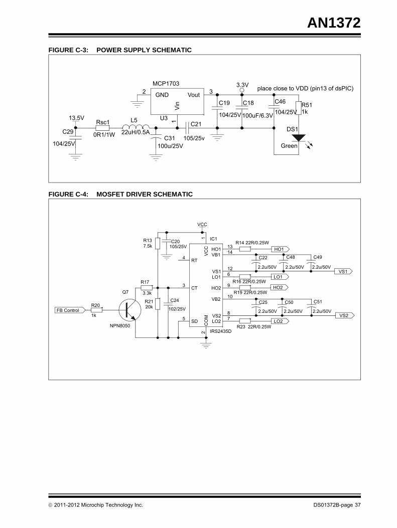
AUXILIARY POWER SYSTEM DESIGNThere are two auxiliary powers, one is 3.3V whichsupplies the digital signal controller and the op amp.The other is 15V, which supplies the full-bridgeMOSFET driver. Figure 23 shows the circuit of theauxiliary power system.
The power of the 15V circuit is calculated byEquation 24.
EQUATION 24: THE POWER OF THE 15V AUXILIARY POWER CIRCUIT
Based on Equation 24, the power of the 15V auxiliarypower, P = 1.18W.
FIGURE 23: AUXILIARY POWER SYSTEM CIRCUITS
Wd t⋅( )sin 0.707=
Where:
the resonance frequency is:
and the ignition pulse width is:
Wd t⋅( )sin 0.707=
Wd 1Lp C4⋅
---------------------=
Wd t1 0.24π Wd t2⋅, 0.76π= =⋅⇒
Tw t2 t10.76π 0.24π–
Wd---------------------------------- 0.5μs>=–=
The RMS ignition pulse width is shown in Figure 22.
Where:The leak inductor of the primary inductor: Lp_leak = 0.1 µHThe peak current of the primary inductor: IL_pk = 11.48AOperation frequency: fs = 180 kHz
P 12---Lp_leak IL_pk
2 fs⋅ ⋅=
Vbat
Cin Cout
3.3VMCP1703
3.3V Auxiliary Power Circuit
15V Auxiliary Power Circuit
T1
15V
© 2011-2012 Microchip Technology Inc. DS01372B-page 23
AN1372
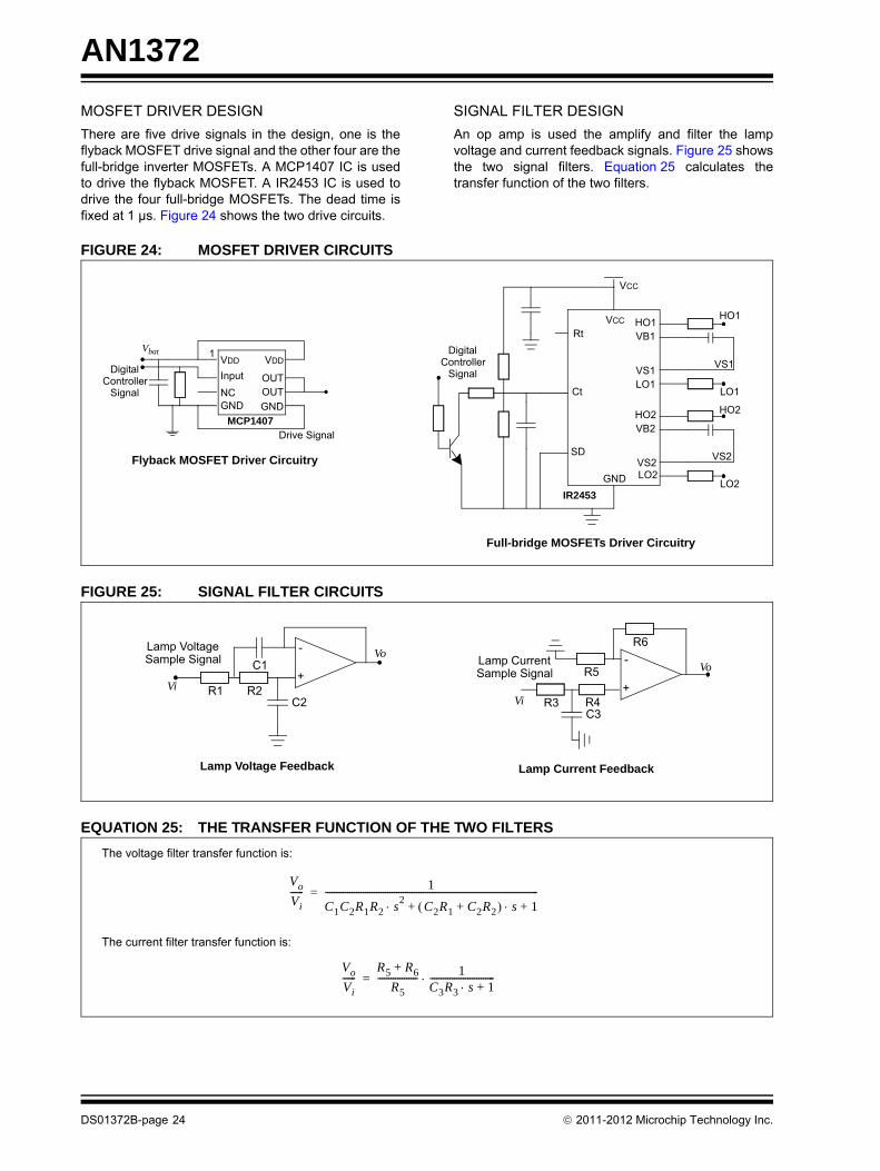
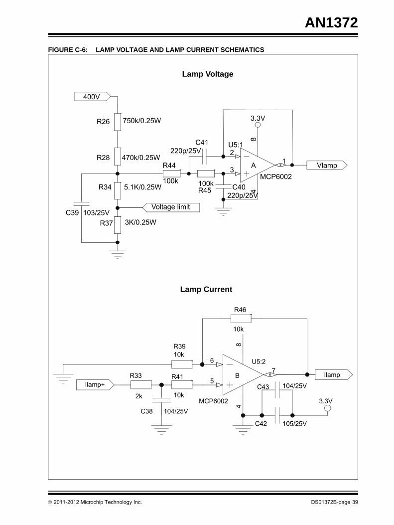
MOSFET DRIVER DESIGNThere are five drive signals in the design, one is theflyback MOSFET drive signal and the other four are thefull-bridge inverter MOSFETs. A MCP1407 IC is usedto drive the flyback MOSFET. A IR2453 IC is used todrive the four full-bridge MOSFETs. The dead time isfixed at 1 µs. Figure 24 shows the two drive circuits.SIGNAL FILTER DESIGNAn op amp is used the amplify and filter the lampvoltage and current feedback signals. Figure 25 showsthe two signal filters. Equation 25 calculates thetransfer function of the two filters.
FIGURE 24: MOSFET DRIVER CIRCUITS
FIGURE 25: SIGNAL FILTER CIRCUITS
EQUATION 25: THE TRANSFER FUNCTION OF THE TWO FILTERS
MCP1407
VDD VDD1
InputNCGND GND
OUTOUT
Vbat
Drive Signal
DigitalController
Signal
Rt
Ct
SD
IR2453
VCC
GND
HO1VB1
VS1LO1
HO2VB2
VS2LO2
VCC
DigitalController
SignalVS1
VS2
HO1
LO1
HO2
LO2
Flyback MOSFET Driver Circuitry
Full-bridge MOSFETs Driver Circuitry
+
-
C2R2R1
C1Lamp VoltageSample Signal Vo
Vi +
-R5
R6
Vo
R4R3C3
Lamp CurrentSample Signal
Vi
Lamp Voltage Feedback Lamp Current Feedback
The voltage filter transfer function is:
The current filter transfer function is:
VoVi------ 1
C1C2R1R2 s2 C2R1 C2R2+( ) s 1+⋅+⋅------------------------------------------------------------------------------------------------=
VoVi------
R5 R6+R5
------------------ 1C3R3 s 1+⋅-----------------------------⋅=
DS01372B-page 24 © 2011-2012 Microchip Technology Inc.
AN1372
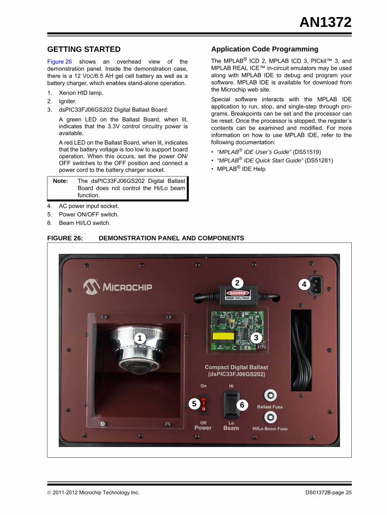
GETTING STARTEDFigure 26 shows an overhead view of thedemonstration panel. Inside the demonstration case,there is a 12 VDC/6.5 AH gel cell battery as well as abattery charger, which enables stand-alone operation.
1. Xenon HID lamp.2. Igniter.3. dsPIC33FJ06GS202 Digital Ballast Board:
A green LED on the Ballast Board, when lit,indicates that the 3.3V control circuitry power isavailable.A red LED on the Ballast Board, when lit, indicatesthat the battery voltage is too low to support boardoperation. When this occurs, set the power ON/OFF switches to the OFF position and connect apower cord to the battery charger socket.
4. AC power input socket.5. Power ON/OFF switch.6. Beam HI/LO switch.
Application Code ProgrammingThe MPLAB® ICD 2, MPLAB ICD 3, PICkit™ 3, andMPLAB REAL ICE™ in-circuit emulators may be usedalong with MPLAB IDE to debug and program yoursoftware. MPLAB IDE is available for download fromthe Microchip web site.
Special software interacts with the MPLAB IDEapplication to run, stop, and single-step through pro-grams. Breakpoints can be set and the processor canbe reset. Once the processor is stopped, the register’scontents can be examined and modified. For moreinformation on how to use MPLAB IDE, refer to thefollowing documentation:
• “MPLAB® IDE User’s Guide” (DS51519)• “MPLAB® IDE Quick Start Guide” (DS51281)• MPLAB® IDE Help
FIGURE 26: DEMONSTRATION PANEL AND COMPONENTS
Note: The dsPIC33FJ06GS202 Digital BallastBoard does not control the Hi/Lo beamfunction.
1
2 4
3
5 6
© 2011-2012 Microchip Technology Inc. DS01372B-page 25
AN1372
Programming the ApplicationComplete the following steps to program thedemonstration board:1. Make sure that the Power ON/OFF switch is inthe OFF position.
2. Connect the emulator header to the 6-pinconnector labeled ICD_1.
FIGURE 27: EMULATOR CONNECTOR POSITION
3. Set the Power ON/OFF switch to the ONposition.
4. Start MPLAB IDE and open the HID Ballastdemonstration project by double-clickingthe .mcw file. The remaining steps take placewithin MPLAB IDE.
5. Build the project by selecting Project > Build All.6. Choose the desired programmer, such as
MPLAB ICD 3, by selecting Programmer >Select Programmer.
7. Program the device by selecting Programmer >Program.
8. After the device has been programmed, set thePower ON/OFF switch to the OFF position.
9. Disconnect the emulator header from the 6-pinconnector labeled ICD1_1.
The HID Ballast board is now programmed and readyto run the demonstration.
Running the Application DemonstrationsThis section describes two different automotiveheadlight demonstrations:
• HID lamp operation with full digital control• Hi/Lo-beam operation
Both of these demonstrations can be run eithersimultaneously or separately using the following steps(refer to Figure 26 for switch locations):
1. To operate the HID lamp, use the Power ON/OFF switch.
When the lamp is switched on, a high-pitchedbuzzing noise may be present at the start ofballast operation. This is normal and is not acause for concern.
2. To check hot lamp operation, do the following: a) Run the lamp for at least one minute to
bring the lamp to a high temperature. b) After one minute, turn the HID lamp off by
setting the Power ON/OFF switch to theOFF position.
c) Wait for a few seconds and then set thePower ON/OFF switch to the ON position.The lamp should light immediately.
3. To check cool lamp operation, do the following: a) Make sure the HID lamp is cold. The lamp
should be switched to the OFF position forat least 10 minutes.
b) Set the Power ON/OFF switch to the ONposition. The lamp should light immediately.
4. To run the Hi/Lo-beam demonstration, simplytoggle the Hi/Lo-beam ON/OFF switch.
Note: When debugging the HID Ballast with theemulator, the connection between the PCand the board can be lost due to noiseinterference from lamp ignition. Therefore,it is recommended to use Programmingmode.
Warning: When the lamp is lit, the light emitted isvery strong, which may cause physicalharm to your eyes.
In addition, the lamp tube may rise to avery high temperature in just a few sec-onds. Do not touch the lamp or allowany flammable objects to come incontact with the lamp tube.
FAILURE TO HEED THESEWARNINGS COULD RESULT INPROPERTY DAMAGE OR BODILYHARM.
DS01372B-page 26 © 2011-2012 Microchip Technology Inc.

AN1372
LABORATORY TEST RESULTS AND WAVEFORMSTable 8 summarizes the resources required by the HIDBallast design in terms of memory size, peripherals,MIPS, etc.
TABLE 8: dsPIC RESOURCE USAGE
The final prototype of the automotive HID ballast wastested according to the technical requirements. Thetest results are shown in Table 9. The testing conditionsare as follows:
• Test lamp: Xenon HID lamp, 35W, color temperature 6000K.
• Ambient temperature: 25ºC, ±5ºC• Test input voltage: 9V-16V• Rated voltage: 13.5V• Oscilloscopes: YOKOGAWA DLM2024• Voltage source: Chroma 62024P-80-60
Figure 28 through Figure 37 show the variouswaveforms including lamp current, voltage and powerfrom the turn-on stage to the steady state, and providesa magnified view in every stage. In addition, the ignitioncurve and the input current curve are shown to verifythe reference design.
TABLE 9: TEST RESULTS
Resource Value
Program Memory 2409 bytesData Memory 48 bytesPWM 1 channelADC 3 channelsComparator 2 channelsMIPS 33.6I/O 2 channels
Characteristic Test Result CommentsInput Voltage Nominal (13.5V) Passed —
Operation (9V-16V) Passed —Temperature Operation (-40ºC to 105ºC) Passed —Transient Maximum Output Current 1.8A VIN = 9.4V-16V
Maximum Input Power 101W VIN = 9.4VMaximum Output Power 82.5W VIN = 13.5V
78W VIN = 16V83.5W VIN = 9.4V
Light Output 70.2W VIN = 13.5V67.2W VIN = 16V
Input Current 3A VIN = 13.5VSteady Output Power 35W VIN = 13.5V
Time to reach steady light output Passed ≤ 150sEfficiency 85.91% VIN = 13.5VAcoustic Resonance No —
Flicker Restrike 100% —Reliability Successive Operating Passed —
Undervoltage Protection 9.4V —Input Protection Overvoltage Protection 16V —
Short Circuit Protection 3A —Output Protection Open Circuit Protection 360V —
© 2011-2012 Microchip Technology Inc. DS01372B-page 27

AN1372
FIGURE 28: IGNITOR OUTPUT VOLTAGE WAVEFORMFIGURE 29: INPUT CURRENT DURING START-UP PROCESS ON A COLD LAMP
Voltage scale: 10kv/div Time scale: 500ns/div
Current scale: 2A/div Time scale: 2s/div
DS01372B-page 28 © 2011-2012 Microchip Technology Inc.

AN1372
FIGURE 30: OPEN VOLTAGE WAVEFORM AND IGNITION FAILED PROTECTIONFIGURE 31: DC BUS VOLTAGE (SUCCESSFUL IGNITION) OF BREAKOVER POINT
Voltage scale: 100V/div Time scale: 200ms/div, 5ms/div
Voltage scale: 100V/div Time scale: 1s/div, 10ms/div
© 2011-2012 Microchip Technology Inc. DS01372B-page 29
AN1372
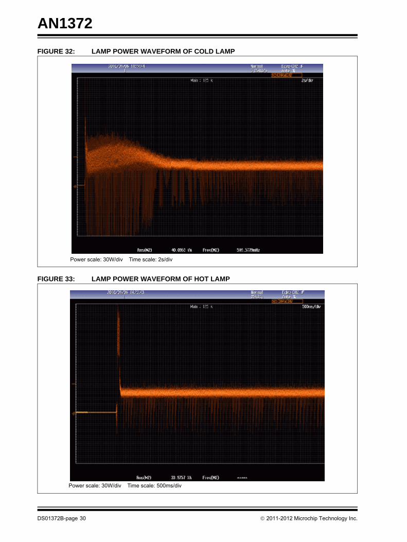
FIGURE 32: LAMP POWER WAVEFORM OF COLD LAMPFIGURE 33: LAMP POWER WAVEFORM OF HOT LAMP
Power scale: 30W/div Time scale: 2s/div
Power scale: 30W/div Time scale: 500ms/div
DS01372B-page 30 © 2011-2012 Microchip Technology Inc.

AN1372
FIGURE 34: CURRENT FOR COLD LAMP; ZOOM OF THE TAKE-CURRENTFIGURE 35: CURRENT AND VOLTAGE FOR COLD LAMP; ZOOM OF THE DC WARM-UP CURRENT
Current scale: 1A/div Time scale: 2s/div, 500us/div
Voltage scale: 100V/div Current scale: 1A/div Time scale: 2s/div, 10ms/div
© 2011-2012 Microchip Technology Inc. DS01372B-page 31

AN1372
FIGURE 36: CURRENT AND VOLTAGE FOR COLD LAMP; ZOOM OF THE RUN-UP STAGEFIGURE 37: CURRENT AND VOLTAGE FOR COLD LAMP; ZOOM OF THE STEADY STATE
Voltage scale: 100V/div Current scale: 1A/div Time scale: 2s/div, 10ms/div
Voltage scale: 100V/div Current scale: 1A/div Time scale: 2s/div, 10ms/div
DS01372B-page 32 © 2011-2012 Microchip Technology Inc.

AN1372
SUMMARYThe reference design presented in this application noteshows a complete fully digital controlled HID ballastdesign with simple circuitry and fast response. TheMicrochip dsPIC DSC device used in this referencedesign provides all of the necessary features andperipherals to implement a high-performance HIDballast. Its 40 MHz DSP engine is fast enough toimplement real-time power loop control. Together withthe on-chip Intelligence power peripheral modules(High-Speed ADC, Comparator, PWM), differentcontrol loops combined with precise timing control waseasily implemented. Fast and smooth transitionbetween different loops was also developed. The initialarc was successfully detected, and the subsequent fastresponse was provided to maintain it. In addition,system diagnose and fault protection can also beimplemented without extra components.
Note: Future plans for this application noteinclude the addition of MATLAB modelinginformation. Please continue to check theMicrochip web site for updates.
© 2011-2012 Microchip Technology Inc. DS01372B-page 33

AN1372
APPENDIX A: SOURCE CODE
All of the software covered in this application note isavailable as a single WinZip archive file. This archivecan be downloaded from the Microchip corporate Website at:
www.microchip.com
APPENDIX B: REVISION HISTORY
Revision A (March 2011)This is the initial released version of the document
Revision B (April 2012)This revision includes the following updates:
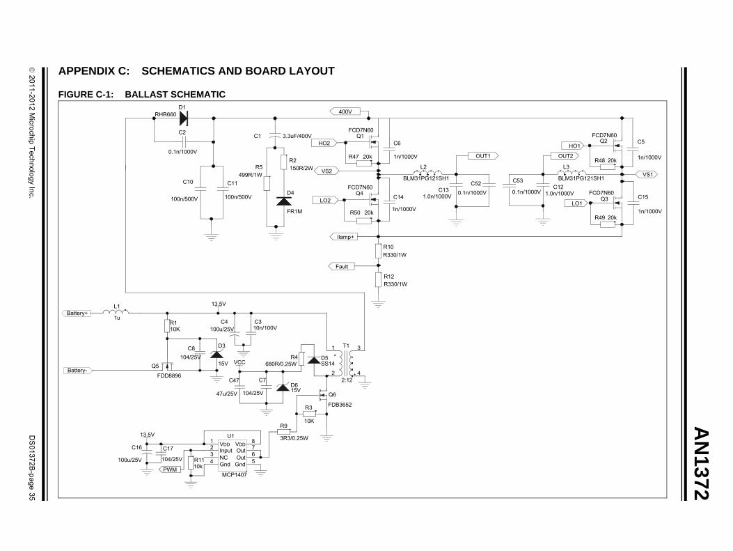
• The “Getting Started” section and the Ballast Schematic (see Figure C-1) were updated to reflect hardware changes made to the reference design
• In addition, formatting and text changes were incorporated throughout the document for clarification purposes
Software License AgreementThe software supplied herewith by Microchip Technology Incorporated (the “Company”) is intended and supplied to you, theCompany’s customer, for use solely and exclusively with products manufactured by the Company.The software is owned by the Company and/or its supplier, and is protected under applicable copyright laws. All rights are reserved.Any use in violation of the foregoing restrictions may subject the user to criminal sanctions under applicable laws, as well as to civilliability for the breach of the terms and conditions of this license.THIS SOFTWARE IS PROVIDED IN AN “AS IS” CONDITION. NO WARRANTIES, WHETHER EXPRESS, IMPLIED OR STATU-TORY, INCLUDING, BUT NOT LIMITED TO, IMPLIED WARRANTIES OF MERCHANTABILITY AND FITNESS FOR A PARTICU-LAR PURPOSE APPLY TO THIS SOFTWARE. THE COMPANY SHALL NOT, IN ANY CIRCUMSTANCES, BE LIABLE FORSPECIAL, INCIDENTAL OR CONSEQUENTIAL DAMAGES, FOR ANY REASON WHATSOEVER.
DS01372B-page 34 © 2011-2012 Microchip Technology Inc.
© 2011-2012 M
icrochip Technology Inc.D
S01372B
-page 35
AN
1372
A
F
C5
1n/1000V
C15
1n/1000V
Q2FCD7N60
Q3FCD7N60
C121.0n/1000V
L3
BLM31PG121SH1
R48 20k
R49 20k
OUT2
C53
0.1n/1000V
LO1
HO1
VS1
PPENDIX C: SCHEMATICS AND BOARD LAYOUT
IGURE C-1: BALLAST SCHEMATIC
VDD1
Input2
NC3
Gnd4
VDD8
Out 7
Out 6
Gnd 5
U1
MCP1407
C17
104/25V
L1
1u
D4
FR1M
1 3
2 4
*
*
T1
2:12
R5499R/1W
R12R330/1W
D3
15V
R110K
C8104/25V
C6
1n/1000V
C14
1n/1000V
Q5
FDD8896
Q1FCD7N60
Q4FCD7N60
PWM
C310n/100V
R1110k
C11
100n/500V
R9
3R3/0.25W
D1RHR660
Q6
FDB3652
13.5V
C4100u/25V
D5SS14
R4680R/0.25W
C47
47u/25V
13.5V
C2
0.1n/1000V
C1 3.3uF/400V
L2
BLM31PG121SH1
C131.0n/1000V
R10R330/1W
C16
100u/25V
R47 20k
R50 20k
R2150R/2W
C10
100n/500V
D615V
C7
104/25V
VCC
R3
10K
Battery+
Battery-
OUT1
400V
HO2
LO2
Fault
C520.1n/1000V
Ilamp+
VS2

AN
1372
DS
01372B-page 36
© 2011-2012 M
icrochip Technology Inc.
FIGURE C-2: dsPIC® DSC DEVICE SCHEMATIC
C26104/25V
FB Control
PWM
R15
0R
30uF/6.3V
C27104/25V
3.3VL4
DS2
Red
MCLR1AN0/CMP1A/RA02
AN1/CMP1B/RA13
AN2/CMP1C/CMP2A/RA24
AN3/CMP1D/CMP2B/RB05
AN4/CMP2C/RB96
AN5/CMP2D/RB107
VSS8
OSCI/CLKIN/RB19 OSCO/CLKO/RB210
PGD2/EMUD2/DACOUT/INT0/RB3 11
PGC2/EMUC2/EXTREF/RB412
VDD13
PGD3/EMUD3/RB814
PGC3/EMUC3/RB15 15
TDO/RB5 16
PGD1/EMUD1/TDI/SCL/RB6 17
PGC1/EMUC1/SDA/RB718
VSS19
VCAP20
TMS/RB11 21
TCK/RB12 22
PWM2H/RB13 23
PWM2L/RB14 24
PWM1H/RA425
PWM1L/RA326
AVSS27
AVDD 28
U2
dsPIC33FJ06GS202
MCLPEMUDEMUC
Voltage limit
VlampIlamp
C310
Vin
C32
104/25V
C28
102/25V
Current Protection
3.3V
C45
105/25V
C44
104/25V
R52 1k
AN1372
FIGURE C-3: POWER SUPPLY SCHEMATICFIGURE C-4: MOSFET DRIVER SCHEMATIC
Vout 3
Vin
1
GND2
U3
MCP1703
C18
100uF/6.3VC21
105/25v
3.3V
L5
22uH/0.5AC31
100u/25V
13.5V
C29
104/25V
C19
104/25V
C46
104/25V
place close to VDD (pin13 of dsPIC)
Rsc1
0R1/1W
R511k
DS1
Green
VC
C1
CO
M2
CT3
RT4
SD5
LO1 6
LO2 7VS2 8
HO2 9
VB2 10
VS1 12
HO1 13
VB1 14
IC1
IRS2435D
C20105/25V
R137.5k
R14 22R/0.25W
C24
102/25V
R19 22R/0.25W
R16 22R/0.25W
R23 22R/0.25W
VCC
FB Control
R2120k
R17
3.3k
R20
1k
Q7
NPN8050
C25
2.2u/50V
C22
2.2u/50V
LO1
HO1
HO2
LO2VS2
VS1
C48
2.2u/50V
C49
2.2u/50V
C50
2.2u/50V
C51
2.2u/50V
© 2011-2012 Microchip Technology Inc. DS01372B-page 37

AN1372
FIGURE C-5: DEBUGGER, INPUT VOLTAGE, AND OVERCURRENT SCHEMATICSVPPVDDVSSDATCLONC
ICD
Header 6H
EMUDEMUC
R274.7K
C34
105/25V
Vin
R29
20k
R35 2k
R32
1k
C37 104/25V
13.5V
MCLP
Current Protection
R30
2k
C36 104/25V
3.3V
Fault
Debugger
Input Voltage
Overcurrent
DS01372B-page 38 © 2011-2012 Microchip Technology Inc.
AN1372
FIGURE C-6: LAMP VOLTAGE AND LAMP CURRENT SCHEMATICSR28 470k/0.25W
R34 5.1K/0.25W
Vlamp
R33
2k
C38 104/25V
Ilamp
R26 750k/0.25W
C39 103/25VR37 3K/0.25W
Voltage limit
R45100k
R44
100kC40
220p/25V
C41220p/25V
3.3V
2
31A
84
U5:1
MCP6002
R41
10k
R3910k
R46
10k
C42 105/25V
C43 104/25V5
67
B
84
U5:2
MCP6002 3.3V
Ilamp+
400V
Lamp Current
Lamp Voltage
© 2011-2012 Microchip Technology Inc. DS01372B-page 39

AN1372
FIGURE C-7: IGNITER CIRCUIT SCHEMATICD112
P1OUT1
OUT2
C1
C2330n/630V
R11K/3W
R2
6.8MR3
6.8M
R46.8M
D2
D3
T1
Trans
SG
600V
12
P2
Connect to Lamp
DS01372B-page 40 © 2011-2012 Microchip Technology Inc.
AN1372
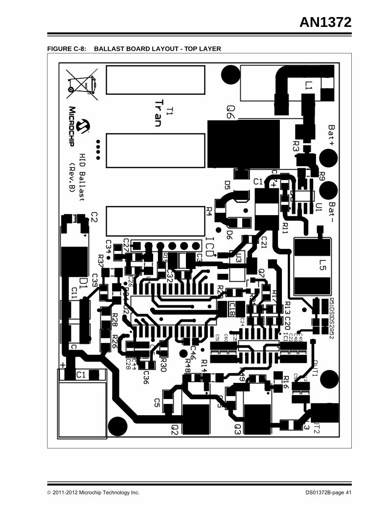
FIGURE C-8: BALLAST BOARD LAYOUT - TOP LAYER© 2011-2012 Microchip Technology Inc. DS01372B-page 41

AN1372
FIGURE C-9: BALLAST BOARD LAYOUT - MIDDLE LAYER 1DS01372B-page 42 © 2011-2012 Microchip Technology Inc.

AN1372
FIGURE C-10: BALLAST BOARD LAYOUT - MIDDLE LAYER 2© 2011-2012 Microchip Technology Inc. DS01372B-page 43
AN1372
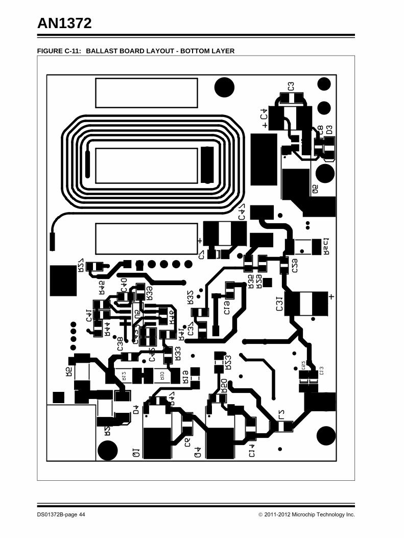
FIGURE C-11: BALLAST BOARD LAYOUT - BOTTOM LAYERDS01372B-page 44 © 2011-2012 Microchip Technology Inc.

AN1372
FIGURE C-12: BALLAST BOARD LAYOUT - TOP SIDE© 2011-2012 Microchip Technology Inc. DS01372B-page 45

AN1372
FIGURE C-13: BALLAST BOARD LAYOUT - BOTTOM SIDEDS01372B-page 46 © 2011-2012 Microchip Technology Inc.

Note the following details of the code protection feature on Microchip devices:• Microchip products meet the specification contained in their particular Microchip Data Sheet.
• Microchip believes that its family of products is one of the most secure families of its kind on the market today, when used in the intended manner and under normal conditions.
• There are dishonest and possibly illegal methods used to breach the code protection feature. All of these methods, to our knowledge, require using the Microchip products in a manner outside the operating specifications contained in Microchip’s Data Sheets. Most likely, the person doing so is engaged in theft of intellectual property.
• Microchip is willing to work with the customer who is concerned about the integrity of their code.
• Neither Microchip nor any other semiconductor manufacturer can guarantee the security of their code. Code protection does not mean that we are guaranteeing the product as “unbreakable.”
Code protection is constantly evolving. We at Microchip are committed to continuously improving the code protection features of ourproducts. Attempts to break Microchip’s code protection feature may be a violation of the Digital Millennium Copyright Act. If such actsallow unauthorized access to your software or other copyrighted work, you may have a right to sue for relief under that Act.
Information contained in this publication regarding deviceapplications and the like is provided only for your convenienceand may be superseded by updates. It is your responsibility toensure that your application meets with your specifications.MICROCHIP MAKES NO REPRESENTATIONS ORWARRANTIES OF ANY KIND WHETHER EXPRESS ORIMPLIED, WRITTEN OR ORAL, STATUTORY OROTHERWISE, RELATED TO THE INFORMATION,INCLUDING BUT NOT LIMITED TO ITS CONDITION,QUALITY, PERFORMANCE, MERCHANTABILITY ORFITNESS FOR PURPOSE. Microchip disclaims all liabilityarising from this information and its use. Use of Microchipdevices in life support and/or safety applications is entirely atthe buyer’s risk, and the buyer agrees to defend, indemnify andhold harmless Microchip from any and all damages, claims,suits, or expenses resulting from such use. No licenses areconveyed, implicitly or otherwise, under any Microchipintellectual property rights.
© 2011-2012 Microchip Technology Inc.
QUALITY MANAGEMENT SYSTEM CERTIFIED BY DNV
== ISO/TS 16949 ==
Trademarks
The Microchip name and logo, the Microchip logo, dsPIC, KEELOQ, KEELOQ logo, MPLAB, PIC, PICmicro, PICSTART, PIC32 logo, rfPIC and UNI/O are registered trademarks of Microchip Technology Incorporated in the U.S.A. and other countries.
FilterLab, Hampshire, HI-TECH C, Linear Active Thermistor, MXDEV, MXLAB, SEEVAL and The Embedded Control Solutions Company are registered trademarks of Microchip Technology Incorporated in the U.S.A.
Analog-for-the-Digital Age, Application Maestro, chipKIT, chipKIT logo, CodeGuard, dsPICDEM, dsPICDEM.net, dsPICworks, dsSPEAK, ECAN, ECONOMONITOR, FanSense, HI-TIDE, In-Circuit Serial Programming, ICSP, Mindi, MiWi, MPASM, MPLAB Certified logo, MPLIB, MPLINK, mTouch, Omniscient Code Generation, PICC, PICC-18, PICDEM, PICDEM.net, PICkit, PICtail, REAL ICE, rfLAB, Select Mode, Total Endurance, TSHARC, UniWinDriver, WiperLock and ZENA are trademarks of Microchip Technology Incorporated in the U.S.A. and other countries.
SQTP is a service mark of Microchip Technology Incorporated in the U.S.A.
All other trademarks mentioned herein are property of their respective companies.
© 2011-2012, Microchip Technology Incorporated, Printed in the U.S.A., All Rights Reserved.
Printed on recycled paper.
ISBN: 978-1-62076-213-4
DS01372B-page 47
Microchip received ISO/TS-16949:2009 certification for its worldwide headquarters, design and wafer fabrication facilities in Chandler and Tempe, Arizona; Gresham, Oregon and design centers in California and India. The Company’s quality system processes and procedures are for its PIC® MCUs and dsPIC® DSCs, KEELOQ® code hopping devices, Serial EEPROMs, microperipherals, nonvolatile memory and analog products. In addition, Microchip’s quality system for the design and manufacture of development systems is ISO 9001:2000 certified.

DS01372B-page 48 © 2011-2012 Microchip Technology Inc.
AMERICASCorporate Office2355 West Chandler Blvd.Chandler, AZ 85224-6199Tel: 480-792-7200 Fax: 480-792-7277Technical Support: http://www.microchip.com/supportWeb Address: www.microchip.comAtlantaDuluth, GA Tel: 678-957-9614 Fax: 678-957-1455BostonWestborough, MA Tel: 774-760-0087 Fax: 774-760-0088ChicagoItasca, IL Tel: 630-285-0071 Fax: 630-285-0075ClevelandIndependence, OH Tel: 216-447-0464 Fax: 216-447-0643DallasAddison, TX Tel: 972-818-7423 Fax: 972-818-2924DetroitFarmington Hills, MI Tel: 248-538-2250Fax: 248-538-2260IndianapolisNoblesville, IN Tel: 317-773-8323Fax: 317-773-5453Los AngelesMission Viejo, CA Tel: 949-462-9523 Fax: 949-462-9608Santa ClaraSanta Clara, CA Tel: 408-961-6444Fax: 408-961-6445TorontoMississauga, Ontario, CanadaTel: 905-673-0699 Fax: 905-673-6509
ASIA/PACIFICAsia Pacific OfficeSuites 3707-14, 37th FloorTower 6, The GatewayHarbour City, KowloonHong KongTel: 852-2401-1200Fax: 852-2401-3431Australia - SydneyTel: 61-2-9868-6733Fax: 61-2-9868-6755China - BeijingTel: 86-10-8569-7000 Fax: 86-10-8528-2104China - ChengduTel: 86-28-8665-5511Fax: 86-28-8665-7889China - ChongqingTel: 86-23-8980-9588Fax: 86-23-8980-9500China - HangzhouTel: 86-571-2819-3187 Fax: 86-571-2819-3189China - Hong Kong SARTel: 852-2401-1200 Fax: 852-2401-3431China - NanjingTel: 86-25-8473-2460Fax: 86-25-8473-2470China - QingdaoTel: 86-532-8502-7355Fax: 86-532-8502-7205China - ShanghaiTel: 86-21-5407-5533 Fax: 86-21-5407-5066China - ShenyangTel: 86-24-2334-2829Fax: 86-24-2334-2393China - ShenzhenTel: 86-755-8203-2660 Fax: 86-755-8203-1760China - WuhanTel: 86-27-5980-5300Fax: 86-27-5980-5118China - XianTel: 86-29-8833-7252Fax: 86-29-8833-7256China - XiamenTel: 86-592-2388138 Fax: 86-592-2388130China - ZhuhaiTel: 86-756-3210040 Fax: 86-756-3210049
ASIA/PACIFICIndia - BangaloreTel: 91-80-3090-4444 Fax: 91-80-3090-4123India - New DelhiTel: 91-11-4160-8631Fax: 91-11-4160-8632India - PuneTel: 91-20-2566-1512Fax: 91-20-2566-1513Japan - OsakaTel: 81-66-152-7160 Fax: 81-66-152-9310Japan - YokohamaTel: 81-45-471- 6166 Fax: 81-45-471-6122Korea - DaeguTel: 82-53-744-4301Fax: 82-53-744-4302Korea - SeoulTel: 82-2-554-7200Fax: 82-2-558-5932 or 82-2-558-5934Malaysia - Kuala LumpurTel: 60-3-6201-9857Fax: 60-3-6201-9859Malaysia - PenangTel: 60-4-227-8870Fax: 60-4-227-4068Philippines - ManilaTel: 63-2-634-9065Fax: 63-2-634-9069SingaporeTel: 65-6334-8870Fax: 65-6334-8850Taiwan - Hsin ChuTel: 886-3-5778-366Fax: 886-3-5770-955Taiwan - KaohsiungTel: 886-7-536-4818Fax: 886-7-330-9305Taiwan - TaipeiTel: 886-2-2500-6610 Fax: 886-2-2508-0102Thailand - BangkokTel: 66-2-694-1351Fax: 66-2-694-1350
EUROPEAustria - WelsTel: 43-7242-2244-39Fax: 43-7242-2244-393Denmark - CopenhagenTel: 45-4450-2828 Fax: 45-4485-2829France - ParisTel: 33-1-69-53-63-20 Fax: 33-1-69-30-90-79Germany - MunichTel: 49-89-627-144-0 Fax: 49-89-627-144-44Italy - Milan Tel: 39-0331-742611 Fax: 39-0331-466781Netherlands - DrunenTel: 31-416-690399 Fax: 31-416-690340Spain - MadridTel: 34-91-708-08-90Fax: 34-91-708-08-91UK - WokinghamTel: 44-118-921-5869Fax: 44-118-921-5820
Worldwide Sales and Service
11/29/11