author: sourabh singh chauhan school of physcial sciences...
TRANSCRIPT

Negative group delay
Author:Sourabh Singh ChauhanSchool of PhyscialSciencesNISER,Bhubneswar

Contents
1 Introduction 2
2 Negative group delay 4
3 Experimental Set up 53.1 Pulse generation using IC7555 . . . . . . . . . . . . . . . . . . 53.2 Active low pass filter . . . . . . . . . . . . . . . . . . . . . . . 53.3 Negative group delay circuit . . . . . . . . . . . . . . . . . . . 73.4 Passive low pass filter . . . . . . . . . . . . . . . . . . . . . . 9
4 Simulation results 9
5 Experiment 145.1 Noise reduction . . . . . . . . . . . . . . . . . . . . . . . . . . 195.2 Causality is not violated . . . . . . . . . . . . . . . . . . . . . 20
6 Optics experiment 21
7 Concluding remarks 24
8 Acknowledgement 25
9 Reference 25
1

1 Introduction
Group delay is observed when our signal consists of multiple frequencies.Monochromatic sources are very hard to make. Even in the most monochro-matic sources we observe a finite spread of frequencies. The spread mayoriginate because of finite duration of the siganl or may arise because ofsome inherent noise in the source itself. The spread gives us a superpositionof various frequencies which in turn gives us information about the material.Responce of dispersive medium depends of the frequency of incident wave.The responce may lead to phase accumulation for different frequencies andgive a shift in the output wave. This shift is known as group delay of thematerial. Material’s dissipative properties can be studied by observing theattenuation as a function of frequency. By writting a signal in terms of itscontinuouse fourier components we can write the form of group velocity i.e.the velocity of the envelope which just accumulates a phase as it travels :-
vg =c
n(ω) + ω dndω
Where c is the velocity of light in vaccuum and n(ω) is refractive index.In case of normal dispersion dn/dω > 0 and n > 1 velocity of energy flowis less than. However in regions of anamolous dispersion where dn/dω canbecome negative. This can lead to a group velocity vg > c, it can also makegroup velocity negative (vg < 0). Although vg > c, it is not a superluminalflow. Because of anamolous dispersion we have a region of large dn/dω whichquestions the very definition of group delay. In some anamolous dispersionswe can have sense of group velocity using the ideas of pulse reshaping. Ithas been shown 1that if absorbers are not to thick, a gaussian pulse withcentral frequency around absorption line and a narrow width propagates withabsorption but it more or less retains its shape (same profile) and peakmoves with group velocity even when it is neative. Actually pulse is reshapedas it passes through the medium. The leading edge is less attenuated incomparison to the trailing edge2. Peak of a very highly attenuated pulseafter absorber can emerge even before the input pulse has entered (negativegroup delay). 3
1C.G.B.Garrett and McCumber Phys Rev. A 1, 305(1970)2 For futher study in pulse reshaping after input pulse passes through medium we refer
J.D. Jackson Classical Electrodynamics 3rd edition section 7.113We can’t question causality here because a Gaussian pulse does not have sharply
defined edge.
2

Figure 1: Refractive index as a function of frequency in anamolous region.Phase velocity and group velocity variation is shown.
Figure 2: Change in the shape of the signal as it moves along the medium.Broader signls having many wavelengths (k0L >> 1 where k0 is centralfrequency and L is length of signal.) gets distorted slowly in comparison toa shaprper signal because of differences in slopes.
3

Negative group delays have been observed in absorbing medium, in atomiccrystals, in photonic crystals, active optical fibers, fiber bragg gratings, cor-rugated waveguides, electronic circuits4 and had been well studied also. Theyhave wide area of application in forming controlled optical delay line. Exper-imental difficulties with optical and atomic system makes it hard for us todesign an experiment in laboratory. That’s why we have chosen to demon-strate negative group delay using electronic filters made from active filters.In the follwing sections we will be discussing the requirements of an elec-tronic circuit for the observation of negative group delay, Circuit design,Calculations of transfer function for varius parts of circuit, demonstrationof experimental and simulation results5, demonstration of non-violation ofcausality, and towards the end we give brief examples of optics experimentfor NGD.
2 Negative group delay
Let us consider signal which has a small spread of frequency ( −Ω to +Ω)around the frequency ω0. Let it passe through a medium electronic circuithaving transfer function ˜H(ω). Then the output can be obtained using fol-lowing calculations:-if
Ein(t) =
∫ inf
0
dω ˜E(ω)
is the input signal.
˜Eout(ω) =
∫ inf
0
dω ˜E(ω) ˜H(ω)eiωt
˜Eout(ω) =
∫ inf
0
dω ˜E(ω)A(ω)eiφ(ω)eiωt
If A(ω) ≈ A(ω0) and φω ≈ φω0 + dφdω|ω0
˜Eout(ω) =
∫ inf
0
dω ˜E(ω)A(ω0)eiφ(ω0)eiω(t+
dφdω|ω0 )
Moreover if A(ω0) ≈ 1,
˜Eout(ω) ≈∫ inf
0
dω ˜E(ω)eiφ(ω0)eiω(t+dφdω|ω0 )
4Li Zhan et. al ICOCN2010 China October 20105Results of C++ programs were used to for numerical simulations
4

˜Eout(ω) ≈ Ein(t+ td)eiφ(ω0)
Here we can see that apart from a global phase factor (which is not ob-servable) the input and output at two different times are the same. If td > 0,output preceedes input!! (negative group delay)
3 Experimental Set up
Here we are using an operational amplifier to obtain negative group delay.Non-inverting end and inverting end should be maintained at same voltage.Inverting end gets a feedback from output and input is connected to the noninverting end. Amplified signal gives a positive delay to input there in theoutput we must have negative delay to maintain same voltage.
In the circuit for negative group delay we use IC-7555 to produce a pulsewhich is then fed to two stages of low pass filer, then it is passed throughvarious stages of negetive group delay circuit to get the final output. In orderto reduce noisy signal (which is enhanced in later stages) we use another lowpass filer (RC) at the output of different stages.
3.1 Pulse generation using IC7555
The rectangular input pulse for the circuit was generated using a IC7555timer circuit in monostable configuration.The width of the rectangular pulse = RCln3.
3.2 Active low pass filter
A low frequecy signal is required to observe negative group delay in Oscil-loscope. We have used an active low pass filter named Bessel filter (usingop-amps). There are several active low pass filters. Bessel filer is well suitedfor the experiment because of fast roll off and stability on cascading. Ingeneral active filters are better than passive filters (made by inductors andcapacitors) because the feedback makes them less noisy while using multiplestages. Active filters have many other advantages over passive filters like noattenuation, easy frequency adjustments, no loading problem ( because ofhigh input resistance and low output resistance), less price. For the circuitabove if we consider I2 to be the input current, I1 be the current flowingthrough R1 and C1 and I3 be the curent through upper part of circuit. Then
5

Figure 3: Monostable configuration of IC 7555
Figure 4: Bessel filter circuit diagram
6

Figure 5: IC TL082 used in the confiuration of NGD
considering ideal op-amp behavior we can make and equivalent circuit forthe circuit and infer the following equations after applying Kelvin
′s voltage
law:-
Vin = I2R1 + I1(XC1+R1) (1)
Vout = I3R3 + I1XC1 (2)
Vout = I1R1 + 2I1XC1 − I2XC1 (3)
I3 = −I1XC1
R2
(4)
These equation leads to the transfer function (after substituting I2 and I3 interms of I1 in equation of Vout/Vin) as :-
H =VoutVin
=(R3 +R2)X
2C1
XC1R21R2 + 2R2
2 −R3R2 +R2
(5)
Further on substituting α = 1 + R3/R2, T = R1C1, XC1 = −i/ωC1 weobtain:-
H(ω) =α
1 + iωT (3− α) + (iωT )2(6)
3.3 Negative group delay circuit
We have seen negative group delay can be obtained if we have A(ω) ≈ 1 anda linear relation of phase with the frequency. The active circuit shown here
7

can fulfill the requirements.Let I1 be the current through R
′and C and I2 be the current through I2.
Further after drawing equivalent and applying KVL we obtain the followingrelations :-
Vin = I1R′+ I1XC (7)
Vout − Vin = I2XC′ (8)
Vout − Vin = (I1 − I2)R (9)
I2XC′ = (I1 − I2)R (10)
These equations lead to the transfer fucntion of the form:-
H(ω) = 1 +iωCR
(1 + iωCR′)(1 + iωC ′R)(11)
If we choose R′/R ∼ O(10−2) and C
′/C ∼ O(10−2), transfer function takes
the form:-H(ω) = 1 + iωT = (1 + ω2T 2)eitan
−1(ωT ) (12)
Here T = RC. Terms with R′and C
′become dominant at higher frequencies.
But here we are working with low frequency signals as input of negative groupdelay circuit. Using series expansion for tan inverse function we obtain
H(ω) ≈ (1 +O(ω2T 2))ei(ωT+O(ω3T 3)) ≈ eiωT (13)
So negative delay can be calculated as
td = −dφdω
= −T = −RC < 0 (14)
If the condition of low frequency is not satisfied, the output pulse gets dis-torted because of higher order term. Total transfer function after n stagescan be written as
Hn(ω) = A(ω)nenφ(ω)T = (1 + ω2T 2)n/2enφ(ω)T (15)
This gives
A(ω) ≈ 1 +n2T 2ω2
2
φ(ω) ≈ nωT = Ttotalω
The total time delay varies linearly with cascadin stages. But the pulse keepson getting distorted. To keep A(ω) = 1 we need delay T to scales as 1/
√n
which makes delay to vary as√nT without distortion.
8

The group increases linearly with number of stages. But we observedexperimentally that after four stages non linear effects come into play. Nonlinearity along with increased noise at higher stages makes it harder for usto observe negative group delay. First non linear effect can be seen throughexpansion of tan−1 function.
Hn(ω) = A(ω)nenφ(ω)T = (1 +nω2T 2
2)ein(ωT−
ω3T3
3) (16)
Even higher order terms lead to distortion of signal profile. Therefore wecan’t talk about negative group delay at a very high cascading stage.
3.4 Passive low pass filter
Figure 6: RC filter
As cascading stages increase we not only get slightly distorted pulse butthe noise also increases. In order to remove additional noise in the circuit.We did fourier transform of the signal at higher stages and found out thefrequency compoment with highest contribution. Then we removed the noiseusing an additional RC low pass filter. In principle passive low pass filershould distort the signal profile. But for the chosen values of R, C distortioneffects are negligible upto 8 stages. It reduces noise drastically and improvesthe output signal. We have shown the reduced noise using this filter in thefigures for different stage output of NGD.
4 Simulation results
In order to obtain the simulted results of the expermimental data we useC++ programs. Input pulse from IC 7555 has width of 1.64 s and height
9

Figure 7: Magnitude of transfer function of Bessel function. Transfer functionbecomes 1√
2times its maximum value at ω = 1.6 rad/s.
10

Figure 8: Fourier transform of a rectangular pulse of width 1.64 s and height8.6 V.
of 8.6 V. We use the same signal for numerical analysis. First of all fouriertransform of the signal is obtained. Then we used the transfer function forbessel function (as derived earlier) to get the output of the signal in frequencydomain. Then the output was again changed to time domain using inversefouries transform. The ouput of low pass filter was again taken to fourierdomain and using the transfer function of NGD we got the NGD outputin fourier domain which when converted to time domain gives the desiredoutput of NGD. Similar procedure was followed for all 8 stages of NGD aswell (taking only linear terms). Next the output was fed to a passive low passfilter. We have shown the effect of using the lowpass filter computationallyalso.
11

Figure 9: The output of NGD circuit at various stages. Green color representsthe input signal (i.e. output of bessel filter) and rest are various outputs atvarious stages. Delay at each stage is 220 ms.
12

Figure 10: Comparison of filtered and unfiltered outputs of NGD after 1ststage. The profile remains almost same even after passing through low passfilter.
Figure 11: Comparison of filtered and unfiltered outputs of NGD after 8stages. The profile remains almost same for 8th stges input as well.
13
5 Experiment
We designed the circuit following the circuit diagram as shown in the figure.This circuit diaram has 4 stages of NGD. We added four more stages of NGDin the circuit. The output of the NGD at each stage passes through a lowpass RC filter (R = 440kΩ, C = 0.2µF → ωcutoff = 11.4Hz) to give the finaloutput from oscilloscope6. The choice for R,C for IC 555 was based on thedesired width of the rectangular pulse (RCln(3)).
A lower cutoff frequency for IC 7555 (by selecting accordingly) can inprovethe negative group delay at various stages. Lower cotoff gives a larger timefor the NGD circuit to respond (Rising edge pulse increases slowly). Variousresuts are shown in the figures below. We got a linear value of group delaysupto 4 stages (with a slope of linear fit 174.2ms per stages). After 4 stages nonlinear effects start becoming prominant leading to lower NGD as expected.At later stages negative group leads to a saturation around 900ms. Thepassive low pass filter used in the circuit gives an additional delay of 40 msbut it reduces noise drastically.
R0 6.8 M Ω C0 0 .22 µ FR1 2.2 M Ω C1 0.22 µ FR2 10kΩ R3 2.2 kωR 1 MΩ C 0.22 µ FR′
10 k Ω C′
22 nF
Table 1: Values of resistances and capacitances used in the experiment
6The coupling for input should be set to DC other wise we get output which looks likedifferential of input signal
14

Figure 12: Circuit diagram upto four stages
15

n Delay1 1802 3603 5404 6805 7406 9007 8808 900
Table 2: Negative Group Delay at the nth stage
Figure 13: Input signal and bessel filter output.
16

Figure 14: Negative group delay in first four stages. Value of delays arerespectively 180ms,360ms,540ms,680ms. Input-Blue, output-red.
17

Figure 15: Negative group delay in stages 5,6,7,8. Value of delays are respec-tively 740ms,900ms,8800ms,900ms. Input-Blue, output-red.
18

0
200
400
600
800
1000
1200
1400
0 1 2 3 4 5 6 7 8
dela
y(in
ms)
no. of stage
Total delay at different cascading stages
straight line fit for first five stages’delays’’delays’
Figure 16: Negative group delay as a fucntion of stages.
5.1 Noise reduction
It is quite evident from the output that noise increases as we go further andfurther in stages. Effects of using low pass filter is also shown. The Fouriertransform of noise gave a dominant frequency abround 50 Hz. Therefore wedecided to block this frequency. As our signal was in a few Hzs, the choiceof 11.8 Hz was good enough to give the less noisy output.
19

Figure 17: Increasing noise as we got to higher stages(when we don’t usea passive filter). Blue signal corresponds to NGD output of stages 1,2,3,4withot filter and red one gives output with filter. Width of signal signifiesthe noise.
5.2 Causality is not violated
As we have mentioned earlier there is no violation of causality. It is theform of transfer function and the reshaping of the input pulse that leads tonegative group delay. In the rising part of the input signal negative groupdelay adds a positive slope which gives us amplification. On the other handin the falling part of the signal negative slope is added leading to decrease inamplitute. Both these effects results in a negative group delay.Smoothness of Gaussian pulse is the key factor in reshaaping of the pulseand giving negative group delay. Therefore we tried to check with a squareinput pulse which is discontinuous. If causality had violated, we should hveseen an advanced output square pulse. But after giving the input pulsewe didn’t observe a delay even the shape of the pulse changes drasticallyespecially on the edges(because of discontinuity). We can also use triangularto see discontinuity Observations on sinusoidal wave can give us quantitativeestimaation of transfer function which will be just a sine wave with small
20

Figure 18: Rectangular pulse input (Blue) for NGD circuit and its outputafter two stages(Red)
addition cosine wave. However quantification of transfer function has alreadybeen done. It matches the experimental results quite well. This good enoughto validate the transefer function. One can do another experiment to showthat causality is intact. If we short input we will see that both the pulse goto zero simultaneously i.e. no output remanant voltages is observed even formilliseconds. This shows that output is the effect of input not cause.
6 Optics experiment
Mach Zehnder experimentSimple experiment can be designed to observe NGD in optical systems7. Herewe will give an example of a Mach Zehnder interferometer which amounts togive same transfer function which we have for the electronic system discussedso far. The set up of the experiment in shown in the figure. If the lengthof longer arms is L/2, there will be a path difference of (2π + 1)L/λ due tolonger distance travelled by one of the signal.Now if we choose the length as nλ where n is an integer, we find that con-structive interference happen at P and destructive interference happens at
7Kitano et.al.
21
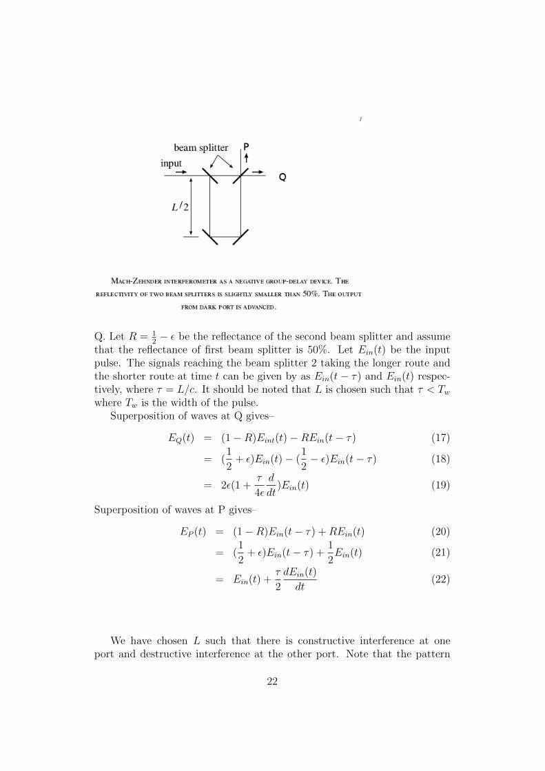
Q. Let R = 12− ε be the reflectance of the second beam splitter and assume
that the reflectance of first beam splitter is 50%. Let Ein(t) be the inputpulse. The signals reaching the beam splitter 2 taking the longer route andthe shorter route at time t can be given by as Ein(t− τ) and Ein(t) respec-tively, where τ = L/c. It should be noted that L is chosen such that τ < Twwhere Tw is the width of the pulse.
Superposition of waves at Q gives–
EQ(t) = (1−R)Eint(t)−REin(t− τ) (17)
= (1
2+ ε)Ein(t)− (
1
2− ε)Ein(t− τ) (18)
= 2ε(1 +τ
4ε
d
dt)Ein(t) (19)
Superposition of waves at P gives–
EP (t) = (1−R)Ein(t− τ) +REin(t) (20)
= (1
2+ ε)Ein(t− τ) +
1
2Ein(t) (21)
= Ein(t) +τ
2
dEin(t)
dt(22)
We have chosen L such that there is constructive interference at oneport and destructive interference at the other port. Note that the pattern
22

Figure 19: The plots are shown for the values ε = 0.06 and τ = 0.0528. Theeight times amplified output of dark port is advanced by 220 ms, preciselythe same for the OPAMP negative delay circuit we made. The values werecomputed using C++.
remains the same only if the input is time independent. If R = 0.5, therewill be an extremely negligible signal at the dark port. Now, change thereflectance of the second beam splitter by a very tiny amount. This could bedone by adding some impurity to its surface or tilting the beam splitter bya very small amount with respect to input beam. Now ε is non zero, secondterm and the first term in the expression have comparable magnitude.Let ususe a Gaussian input source so that the derivative of it is also a Gaussian.Amplified output at the dark port gives more or less same profile as observedin the bright port (which is similar to input). Now output at dark port givesa negative group delay.
Another experiment in optics that can be performed in lab is an experimentbased on the concept of Stimulated Brillouin scattering performed in opticalfibers. 8
8Li Zhan et. al ICOCN2010 China October 2010
23

Figure 20: NGD Circuit
7 Concluding remarks
We have observed the phenomena negative group delay in the electroniccircuit which can tempt us to believe that the causality is violated if wedon’t look at it carefully. We tried to simulate all the results of elecroniccircuit using C++ programs. We were able to reduce noise by an additionalpasive low pass filter. However we don’t quite understand the saturation ofdelay at higher stages. It may be because of cutoff the RC of passive lowpass filter which fixes an uppper bound on maximum negative group delaythat can eb obtained. Optical analogure of the experiment has been shown inprevious section. However it is not possible peform the experiment in the labbecasue of several limitations. In order to get the output in an oscilloscope wefigured out that it is better to work with microwve frequencies. The producea gaussian input for the laser is also a tough task. There have been variousexperiments in microwave frequency using using cavities. Its application inconstant phase shifters has been reported by B.Ravelo et. al. Many otherapplications have also been reported in various references. Next we try tolook for a mechanical analogue of circuit.
24
8 Acknowledgement
This experiment was performed as a part of 8th semester lab course at NISERalong with Maneesha Sushama Pradeep. I would like to say thanks to Ram-prasad sir and Ritwick sir for their guidance during the course of experiment.
9 Reference
• Classical Electrodynamics by J.D. Jackson 3rd edition Chapter
7.
• Wave propagation and group velocity by Leon Brillouin.
• Demonstration of negative group delays in a simple electronic
circuit by T. Nakanishi et. al. 2008
• Li Zhan et. al ICOCN2010 China October 2010, ’NEGATIVE GROUP
VELOCITY SUPERLUMINAL PROPAGATION IN OPTICAL FIBERS USING STIMULATED
BRILLOUIN SCATTERING’
• Phys.Rev. E 66, 056601 2002
• Lab report by Sarmishtha Sahoo, NISER.
• arxiv.org/pdf/quant-ph/0302166
25