aurora's technological and research institute ac lab code
TRANSCRIPT

Auroras Technological and Research Institute AC Lab
Department of ECE 5
CODE OF CONDUCT FOR THE LABORATORIES
All students must observe the Dress Code while in the laboratory
Sandals or open-toed shoes are NOT allowed
Foods drinks and smoking are NOT allowed
All bags must be left at the indicated place
The lab timetable must be strictly followed
Be PUNCTUAL for your laboratory session
Program must be executed within the given time
Noise must be kept to a minimum
Workspace must be kept clean and tidy at all time
Handle the systems and interfacing kits with care
All students are liable for any damage to the accessories due to their own negligence
All interfacing kits connecting cables must be RETURNED if you taken from the lab
supervisor
Students are strictly PROHIBITED from taking out any items from the laboratory
Students are NOT allowed to work alone in the laboratory without the Lab Supervisor
USB Ports have been disabled if you want to use USB drive consult lab supervisor
Report immediately to the Lab Supervisor if any malfunction of the accessories is there
Before leaving the lab
Place the chairs properly
Turn off the system properly
Turn off the monitor
Please check the laboratory notice board regularly for updates
Auroras Technological and Research Institute AC Lab
Department of ECE 6
GENERAL LABORATORY INSTRUCTIONS
You should be punctual for your laboratory session and should not leave the lab without the
permission of the teacher
Each student is expected to have hisher own lab book where they will take notes on the experiments
as they are completed The lab books will be checked at the end of each lab session Lab notes are a
primary source from which you will write your lab reports
Organization of the Laboratory
It is important that the programs are done according to the timetable and completed within the
scheduled time
You should complete the prelab work in advance and utilize the laboratory time for verification only
The aim of these exercises is to develop your ability to understand analyze and test them in the
laboratory
A member of staff and a Lab assistant will be available during scheduled laboratory sessions to
provide assistance
Always attempt program first without seeking help
When you get into difficulty ask for assistance
Assessment
The laboratory work of a student will be evaluated continuously during the semester for 25 marks Of
the 25 marks 15 marks will be awarded for day-to-day work For each program marks are awarded
under three heads
Prelab preparation ndash 5 marks
Practical work ndash 5marks and
Record of the Experiment ndash 5marks
Internal lab test(s) conducted during the semester carries 10 marks
End semester lab examination conducted as per the JNTU regulations carries 50 marks
At the end of each laboratory session you must obtain the signature of the teacher along with the
marks for the session out of 10 on the lab notebook
Lab Reports
Note that although students are encouraged to collaborate during lab each must individually prepare a
report and submit
They must be organized neat and legible
Your report should be complete thorough understandable and literate
You should include a well-drawn and labeled engineering schematic for each circuit investigated
Your reports should follow the prescribed format to give your report structure and to make sure that
you address all of the important points
Graphics requiring- drawn straight lines should be done with a straight edge Well drawn free-hand
sketches are permissible for schematics
Auroras Technological and Research Institute AC Lab
Department of ECE 7
Space must be provided in the flow of your discussion for any tables or figures Do not collect figures
and drawings in a single appendix at the end of the report
Reports should be submitted within one week after completing a scheduled lab session
Presentation
Experimental facts should always be given in the past tense
Discussions or remarks about the presentation of data should mainly be in the present tense
Discussion of results can be in both the present and past tenses shifting back and forth from
experimental facts to the presentation
Any specific conclusions or deductions should be expressed in the past tense
Report Format
Lab write ups should consist of the following sections
Aim
Equipments
Circuit Diagram
Theory
Procedure
Expected Waveform
Observation and Calculations
Results
Conclusions
Note Diagrams if any must be drawn neatly on left hand side
Auroras Technological and Research Institute AC Lab
Department of ECE 8
LIST OF EXPERIMENTS
1 Amplitude Modulation and Demodulation
2 DSB ndash SC Modulator amp Detector
3 SSB-SC Modulator amp Detector (Phase Shift Method)
4 Frequency Modulation and Demodulation
5 Study of Spectrum analyzer and Analysis of AM and FM Signals
6 Pre-emphasis amp De-emphasis
7 Time Division Multiplexing amp De multiplexing
8 Frequency Division Multiplexing amp De multiplexing
9 Verification of Sampling Theorem
10 Pulse Amplitude Modulation amp Demodulation
11 Pulse Width Modulation amp Demodulation
12 Pulse Position Modulation amp Demodulation
13 Frequency Synthesizer
14 AGC Characteristics
15 PLL as FM Demodulator
Annexure I Additional Experiments
1 Characteristics of Mixer
2 Digital Phase Detector
3 Coastas Receiver
Auroras Technological and Research Institute AC Lab
Department of ECE 9
EXPERIMENT NO 1
AMPLITUDE MODULATION amp DEMODULATION OBJECTIVE
To study
1 Amplitude modulation process
2 Measurement of Modulation Index
3 Effect of 100 Modulation over modulation under modulation
4 Demodulation Process
PRE-LAB
1 Study the theory of Amplitude Modulation and Demodulation
2 Draw the circuit diagram for Modulation and Demodulation
3 Draw the expected wave forms for different values of modulation index
COMPONENTS
1 Amplitude Modulation and Demodulation Trainer Kit 1 No 2 CRO Dual Trace 1 No 3 Connecting Probe and Cords
BRIEF THEORY
If you connect a long wire to the output terminals of your Hi-Fi amplifier and another long wire to the input of another amplifier you can transmit music over a short distance DONT try this You could blow up your amplifier
A radio wave can be transmitted long distances To get our audio signal to travel long distances we piggyback it onto a radio wave This process is called MODULATION
The radio wave is called the CARRIER The audio signal is called the MODULATION At the receiving end the audio is recovered by a process called DEMODULATION From the diagram below it can be seen that when the carrier is modulated its amplitude goes above and below its unmodulated amplitude It is about 50 modulated in the
Auroras Technological and Research Institute AC Lab
Department of ECE 10
diagram The maximum percentage modulation possible is 100 Going above this causes distortion
Most broadcasters limit modulation to 80Modulating the carrier frequency with an audio frequency produces two new frequencies At this point it would be a good idea to read the page on MIXERS These new frequencies are called the upper and lower SIDEBANDS The upper sideband is the carrier frequency plus the audio frequency The lower side band is the carrier frequency minus the audio frequencySince the audio signal is not a single frequency but a range of signals (usually 20 Hz to 20 KHz) the sidebands are each 20Hz to 20 KHz wide
If you tune across a station in the Medium Wave Band you will find that it takes up space in the band This is called the signal BANDWIDTH This is the space taken by the upper and lower sidebands In the the example given above it would be 40 KHz Since the Medium Wave is only 500 KHZ wide there would only be space for about 12 stations Therefore the bandwidth of stations is limited to 9 KHz which limits the audio quality If there are two stations too close together their sidebands mix and produce HETERODYNE whistles Since both sidebands carry
Auroras Technological and Research Institute AC Lab
Department of ECE 11
CIRCUIT DIAGRAMS
AM MODULATION
AM DEMODULATION
CARRIER SIGNAL
TIME T
A
m
p
l i t u
d
e
Ac
Auroras Technological and Research Institute AC Lab
Department of ECE 12
MODULATING SIGNAL
AM MODULATED OUTPUT
AM DEMODULATION OUTPUT
PROCEDURE
A MODULATION i Switch lsquoONrsquo the Trainer Kit
ii Generate the carrier and modulating signal such that carrier frequency must be greater than modulating frequency
iii Apply the carrier and modulating signal into AM modulator input vi Trace the envelope of the modulated waveform
v Repeat step(vi) duly adjusting the modulating signal for under modulation and over modulation
B DEMODULATION
i Apply the modulated AM output into Demodulation input ii Trace the demodulated output waveform
POST- LAB
TIME T
A
m
p
l i t u
d
e
Am
A
m
p
l i t u
d
e
TIME T
Auroras Technological and Research Institute AC Lab
Department of ECE 13
i Observe the frequency and amplitude of the carrier and modulating signal
ii Observe the frequency and maximum peak-peak amplitude(Amax) and minimum peak-
peak amplitude (Amin) of the AM signal in TableI
iii Calculate the modulation index Ч=Amax-AminAmax+Amin
iv Plot the out put waveforms Time T Vs Voltage Vo
v Write result and conclusion
CONCLUSION Hence the AM modulation and demodulation is verified
QUESTIONS 1 what is meant by modulation
2 What is meant by modulation index
3 What is meant by under modulation and over modulation
Auroras Technological and Research Institute AC Lab
Department of ECE 14
EXPERIMENT NO 2
DSB ndash SC Modulator amp Demodulator
OBJECTIVE To study the balanced modulator using IC 1496
PRE-LAB
1 Study the theory of balanced modulator
2 Draw the circuit diagram
3 Draw the expected waveforms
4 Study the datasheet of IC 1496
EQUIPMENT
1 Function generator
2 Dual trace CRO
3 Balanced modulator trainer kit
THEORY
In a balanced modulator a signal is modulated using two carriers that are 180
degrees out of phase The resulting signals are then combined in such a way that the carrier
components cancel leaving a DSB-SC (double sideband suppressed carrier) signal
CIRCUIT DIAGRAM
Auroras Technological and Research Institute AC Lab
Department of ECE 15
BALANCED MODULATOR OUTPUT
Auroras Technological and Research Institute AC Lab
Department of ECE 16
BALANCED DEMODULATOR OUTPUT
PROCEDURE
1 Switch ON the trainer kit
2 Generate the carrier and modulating signal
3 Apply the modulating signal and the carrier signal to the balanced modulator input
4 Observe the balanced modulator output
POST LAB
1 Observe the frequency and amplitude of the carrier and modulating signal
2 Observe the frequency and amplitude of the balanced modulator output
3 Observe the quadrature null effect
4 Plot the output waveforms Time T VS Voltage V
5 Write result and conclusions
CONCLUSIONS The balanced modulator output is verified
QUESTIONS 1 what is the efficiency for DSB SC signal
2 What are the other types of balanced modulators
3 What is meant by pilot carrier
Auroras Technological and Research Institute AC Lab
Department of ECE 17
EXPERIMENT NO 3
SSB ndash SC MODULATOR amp DEMODULATOR
OBJECTIVE To study the Single side band modulation by using Phase shift method and demodulation using synchronous detector method
PRE-LAB
1 Study the theory of SSB
2 Draw the circuit diagram and expected waveforms
EQUIPMENTS 1 Function generator 2
2 Dual trace CRO 1
3 SSB system modulation and demodulation trainer kit 4 Patch CardsConnecting wires
5 Frequency counterMulti meter
THEORY
Single-sideband modulation (SSB) is a refinement of amplitude modulation that more
efficiently uses electrical power and bandwidth It is closely related to vestigial sideband
modulation (VSB)Amplitude modulation produces a modulated output signal that has
twice the bandwidth of the original baseband signal Single-sideband modulation avoids
this bandwidth doubling and the power wasted on a carrier at the cost of somewhat
increased device complexity SSB was also used over long distance telephone lines as part
of a technique known as frequency-division multiplexing (FDM) FDM was pioneered by
telephone companies in the 1930s This enabled many voice channels to be sent down a
single physical circuit for example in L-carrier SSB allowed channels to be spaced
(usually) just 4000 Hz apart while offering a speech bandwidth of nominally 300ndash
3400 Hz Amateur began serious experimentation with SSB after World War II The
Strategic Air Command established SSB as the radio standard for its bombers in 1957[4]
It
has become a de facto standard for long-distance voice radio transmissions since then
Auroras Technological and Research Institute AC Lab
Department of ECE 18
BLOCK DIAGRAM OF SSB MODULATOR
SSB-DEMODULATOR SYSTEM
EXPECTED WAVEFORMS
Auroras Technological and Research Institute AC Lab
Department of ECE 19
DSB-SC 0UTPUT
SSB-SC OUTPUT
PROCEDURE
a Modulation
1 Switch ON the trainer kit 2 Observe the output of RF generator using CROThere are two outputs from the RF
generator one is direct output and another is 90 deg phase shift with the direct output 3 Observe the output of AF generator using CROThere are two outputs from the AF
generator one is direct output and another is 90 deg phase shift with the direct output 4 Set the amplitude of the RF signal to 01vpp and connect the 0 deg phase shift signal to
one BM and 90 deg angle phase shift signal to the second BM
5 Set the AF Signal amplitude to 8vpp and connect to the BM 6 Observe the outputs of both balanced modulators simultaneously and adjust the balance
control until get the output waveforms (DSB SC) 7 To get LSB of SSB connect both balanced modulators outputs to SUBTRACTED circuit 8 Measure the frequencies of LSB using multimeter 9 Calculate the theoretical frequency of the SSB (LSB) and compare it with the practical
value LSB=RE Frequency ndashAF Frequency
10 To get USB of SSB signal connect both balanced modulators outputs to ADDER circuit 11 Measure the frequencies of USB
12 Calculate the theoretical value of the SSB Upper Side Band (SSB-USB) frequency and compare it with practical value
USB=RF Frequency+AF Frequency
Auroras Technological and Research Institute AC Lab
Department of ECE 20
b Demodulation (Synchronous detector)
1 Connect the SSB signal from the summer or sub tractor to the SSB signal input of the synchronous detector and RF signal (0ordm) to the RF input of the synchronous detector
2 Observe the Detector output using CRO and compare it with the AF signal (Modulating Signal)
3 Observe the SSB signal for the different frequencies of the AF signal (modulating signal)
TABULATION RF Frequency (Fc) =--------------------KHz
USB LSB
SNo AFsig
Freq(Fm) Practical Freq Theoretical
Freq=Fc+Fm
Practical Freq
Theoretical Freq=Fc-Fm
POST LAB
1 Observe the frequency and amplitude of the RF carrier both (900 amp 0 0 ) phase AF modulating signal (900 amp 0 0 ) phase DSB-SC SSB-SC LSB and USB of the SSB signal
2 Observe the frequency components and bandwidth of SSB
3 Plot the output waveforms above mentioned 4 Write result and conclusion
CONCLUSIONS Hence various outputs of SSB modulator are obtained
QUESTIONS 1 What are the advantages of SSB over AM
2 What is the main drawback of SSB
3 What is meant by VSB
Auroras Technological and Research Institute AC Lab
Department of ECE 21
EXPERIMENT NO 4
FREQUENCY MODULATION AND DEMODULATION
OBJECTIVE To study
1 Frequency modulation process
2 Measurement of Modulation Index
3 Measurement of Frequency deviation
4 Demodulation Process
PRE-LAB 1 Study the data sheet of IC LM 2206 LM 565
2 Study the theory of FM modulation and demodulation
3 Draw the circuit diagram for modulation and demodulation
4 Draw the expected wave forms
EQUIPMENT 1 Frequency modulation and demodulation trainer kit 1 No 2 Dual trace CRO 1 No 3 Connecting probe and cords
THEORY
In telecommunications frequency modulation (FM) conveys information over a carrier
wave by varying its frequency (contrast this with amplitude modulation in which the amplitude
of the carrier is varied while its frequency remains constant) In analog applications the
instantaneous frequency of the carrier is directly proportional to the instantaneous value of the
input signal Digital data can be sent by shifting the carriers frequency among a set of discrete
values a technique known as keying The instantaneous frequency of the oscillator and is the
frequency deviation which represents the maximum shift away from fc in one direction
assuming xm(t) is limited to the range plusmn1Although it may seem that this limits the frequencies in
use to fc plusmn fΔ this neglects the distinction between instantaneous frequency and spectral
frequency The frequency spectrum of an actual FM signal has components extending out to
infinite frequency although they become negligibly small beyond a point Carsons rule of
thumb Carsons rule states that nearly all (~98) of the power of a frequency-modulated signal
lies within a bandwidth
Auroras Technological and Research Institute AC Lab
Department of ECE 22
CIRCUIT DIAGRAM
MODULATION
DEMODULATION
Auroras Technological and Research Institute AC Lab
Department of ECE 23
OUT PUT WAVEFORMS
Auroras Technological and Research Institute AC Lab
Department of ECE 24
PROCEDURE a Modulation
i Switch ON the trainer kit ii Generate the carrier and modulating signal iii apply the modulating signal to the frequency modulator iv Trace the FM output
b Demodulation i apply the modulated FM output into Demodulation input ii Trace the demodulated output waveform
TABULATION
SNo
Amplitude of Modulating
Signal(Am) Fmin
Frequency
Deviation
∆f=fc-fmin or fc-fmax
Modulation Index β=∆ffm
POST LAB
1 Observe the frequency and amplitude of the carrier and modulating signal 2 Calculate the frequency deviation by observing Fmax and Fmin
δ=Fc-Fmax or δ=Fc-Fmin
3 Calculate modulation index β= δFm
4 Change the amplitude of the modulating signal and repeat steps 1 to 3 for different values of Am and note down the readings in table-1
5 Plot the output waveforms Time T VS Voltage Vo
6 Write result and conclusion
CONCLUSIONS Hence the frequency modulated output is obtained
QUESTIONS 1 what is meant by angle modulation
2 How FM is different from AM
3 What is meant by Carson Rule
4 What is the maximum modulation index
Auroras Technological and Research Institute AC Lab
Department of ECE 25
EXPERIMENT NO 5
STUDY OF SPECTRUM ANALIZER AND ANALYSIS OF AM amp FM SIGNALS
Auroras Technological and Research Institute AC Lab
Department of ECE 26
Auroras Technological and Research Institute AC Lab
Department of ECE 27
Auroras Technological and Research Institute AC Lab
Department of ECE 28
EXPERIMENT NO 6
PRE EMPHASIS AND DE EMPHASIS
OBJECTIVE To study the operation of Pre-emphasis and De-emphasis circuits
PRE-LAB
1 Study the theory of Pre-emphasis and De-emphasis circuits
2 Draw the circuit diagram
3 Draw the expected waveforms
COMPONENTS
1 Resistors 100kΩ 100Ω
2 Capacitors 1μf 100μf EQUIPMENT 1 Function generator 1
2 Dual trace CRO 1
THEORY Pre-emphasis
Improving the signal to noise ratio by increasing the magnitude of higher frequency
signals with respect to lower frequency signals
De-emphasis
Improving the signal to noise ratio by decreasing the magnitude of higher
frequency signals with respect to lower frequency signals
Transmitters that employ a true FM modulator require a pre emphasis circuit before the
modulator fore the true FM modulator doesnt automatically pre emphasize the audio like
a transmitter that uses a phase modulator A separate circuit is not necessary for pre
emphasis in a transmitter that has a phase modulator because the phase modulator applies
pre emphasis to the transmitted audio as a function of the phase modulator The receivers
De emphasis circuitry takes the unnatural sounding pre emphasized audio and turns it
back into its original response Pre emphasized (discriminator) audio is however available
directly from the audio demodulation (discriminator) circuitry In linking systems many
choose to eliminate the emphasis circuitry to allow better representation of retransmitted
Auroras Technological and Research Institute AC Lab
Department of ECE 29
signals Since the signal has already been pre emphasized (by the user that is
transmitting) and since the receiver you are listening to takes care of the de emphasis
CIRCUIT DIAGRAMS
PRE-EMPHASIS
DE-EMPHASIS
EXPECTED WAVEFORMS
INPUT
TIME T
A
m
p
l i t u
d
e
Am
Auroras Technological and Research Institute AC Lab
Department of ECE 30
OUTPUT
PRE-EMPHASIS
Freq Vs Gain
DE-EMPHASIS
Freq Vs Gain
TIME T
Freq f (Hz)
A
m
p
l i t u
d
e
Am
Auroras Technological and Research Institute AC Lab
Department of ECE 31
TABLE
PRE EMPHASIS
SNo Input Freq
Input Voltage Vi (Volts)
Output Voltage Vo (Volts) Gain=VoVi
Gain in dB
20log(voVi)
DE-EMPHASIS
SNo Input Freq
Input Voltage Vi (Volts)
Output Voltage Vo (Volts)
Gain=VoVi Gain in dB
20log(VoVi)
PROCEDURE a Pre-emphasis
1 Connect the circuit as per the circuit diagram
2 Apply a constant sine wave input across the input terminal of fixed amplitude(Vi) 3 By varying the input frequency note down the output amplitude (Vo) with respect to
input frequency in Table 4 Calculate the gain using the formula
5 Gain =20log (Vo) (Vi) db
b De-Emphasis
1 Connect the circuit as per the circuit diagram
2 Repeat the steps 2 3 amp4
POST LAB
1 Observe the output amplitude for both the pre-emphasis and De-emphasis circuits
2 Calculate the gain in db
3 Plot the frequency versus gain curves on logarithmic graphs for both the circuits
4 Plot the input and output waveforms Time T VS Voltage Vo
5 Write the result and conclusion
CONCLUSIONS Obtained the pre emphasis and de-emphasis outputs
QUESTIONS 1 Observe the out put signal is disturbed by noise what action has to be taken and measure the
output voltage 2 Where we use the pre emphasis circuit 3 Where we use the de emphasis circuit 4 What are the advantages of pre emphasis and de emphasis circuits
Auroras Technological and Research Institute AC Lab
Department of ECE 32
EXPERIMENT NO 7
TIME DIVISION MULTIPLEXING AND DEMULTIPLEXING
AIM To study Time Division Multiplexing and its waveforms
PRE LAB WORK
Study the operation of Time division multiplexer and demultiplexer Draw the block diagram of TDM
Draw the expected graphs of all necessary waveforms ( CH1CH2TDM OP and Demultiplexed OP)
EQUIPMENT
1) Experimental board on TDM
2) Dual Trace CRO 3) Probes
THEORY
Time Division Multiplexing (TDM) is a technique for transmitting serial messages on a signal
transmission channel by dividing the time division into slots One slot for each message The concept
of TDM comes from sampling theorem which enables use to transmit the information contained in the
band limited Signal using sampling of the signal taken uniformly or a rate slightly higher then the
Nyquist rate TDM enables the joint utilization at a common transmission channel by a number of
independent message sources without mutual interference
The different Ip message signals all band limited in WHz by the IP low pass filters and sequentially
sampled at the transmitters by a rotary switch or a comparator The switch makes are complete
revolution in Ts frac12 W extracting are sample from each IP The commutator OP is a PAM waveform
containing individual message sample
It there are N number of IP the pulse to Pulse spacing will be Ts = 1 while the spacing
N Nfs
bw successive samples from each IP is called a frame
At the receiver a similar rotatory switch the decommutator separates the samples and distributes them
to a bank of low-pass filters which in turn is usually electronic and synchronization signals are
provided to keep the distribute in step with the commutant
Auroras Technological and Research Institute AC Lab
Department of ECE 33
EXPECTED GRAPHS
PROCUDURE
1 Connect the OP of the experimental board to one of the channels on CRO 2 Switch ON the experimental board 3 Observe the OP waveforms 4 Vary the values of the resistors R1 R2 and R3 alternative and observe the OP on CRO
RESULT
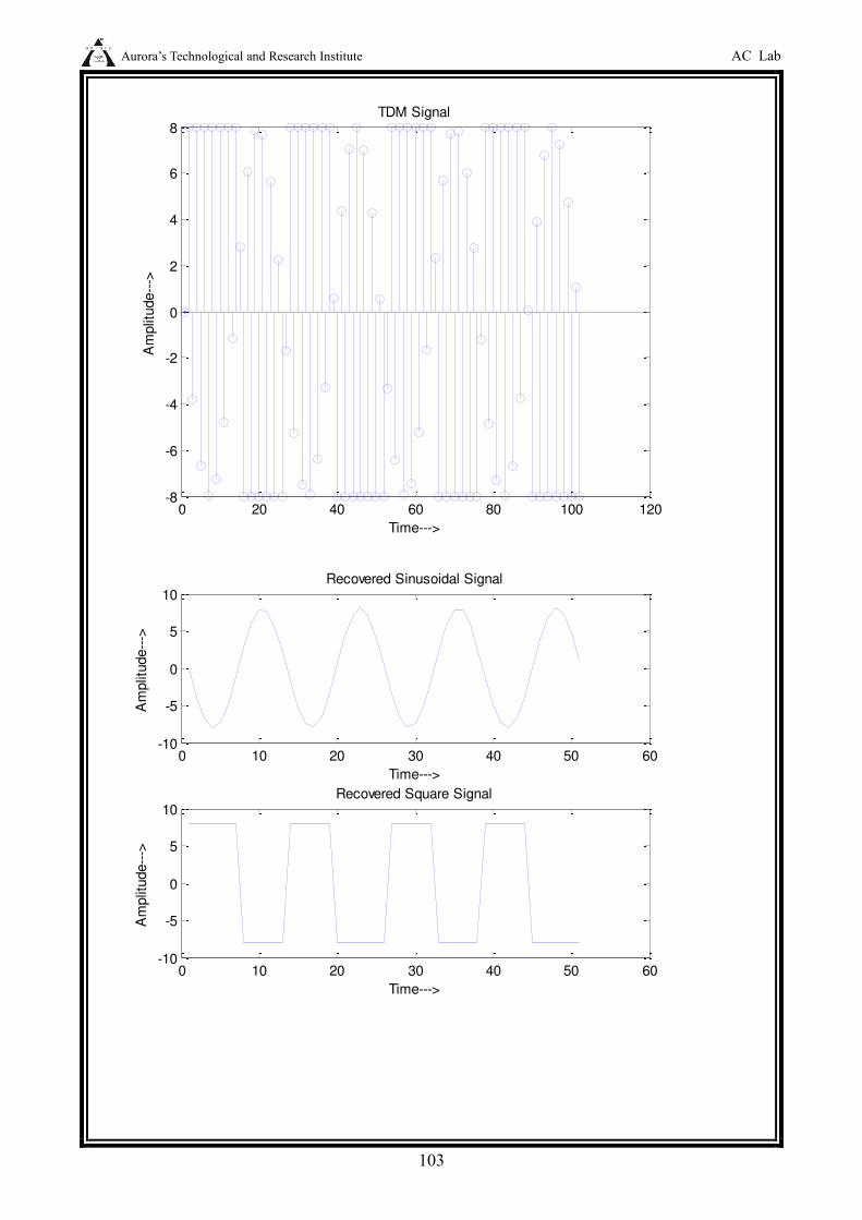
The process of the Time Division Multiplexing and the waveforms has been studied
CONCLUSION
Auroras Technological and Research Institute AC Lab
Department of ECE 34
Figure 1 Time Division Multiplexing amp De multiplexing
Auroras Technological and Research Institute AC Lab
Department of ECE 35
EXPERIMENT NO 9
VERIFICATION OF SAMPLING THEOREM
AIM To study the effect of sampling on the transmission of information through PWM
PRE LAB WORK
Study the sampling theorem
Draw the expected graphs of all necessary waveforms ( message signal carrier wave PWM op demodulated op etc
EQUIPMENT
1) Experimental Board on study of sampling theorem 2) Dual trace CRO (0 ndash 20 MHz) 3) Function Generator 4) Connecting wires
THEORY
The principle of sampling can be explained using the switching sampler The switch periodically shifts below bw two constants at the rate of fs = 1 Ts Hz staying on the IP constant for each sampling period The op Xs(t) of the samples consists of segments of x(t) and Xc(t) can be represented as
Xs(t) = X(t) S(t)
Where S(t) is sampling or switching function There are a number of differences bw the ideal sampling and reconstruction techniques described in the proceeding sections of the actual signal
PROCEDURE
1) Observe the internal clock and measure its frequency and amplitude 2) Give the clock to the clock IP terminal 3) Connect the modulating signal to the IP 4) Check the condition fs gt 2fm and observe the de-modulated wave 5) Check the condition fs lt 2fm and fs = 2fm and draw the OP waveforms
RESULT
CONCLUSION
Aurorarsquos Technological and Research Institute DC Lab
36
Figure 2 Sampling Theorem
Aurorarsquos Technological and Research Institute DC Lab
37
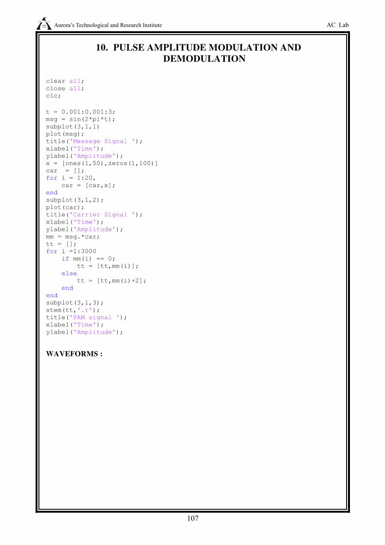
EXPERIMENT NO 10
PULSE AMPLITUDE MODULATION AND DEMODULATION
AIM 1) To study the PAM modulation and its waveforms
2) To study the de-modular of PAM
3) To study the effect of sampling frequency on de-modulation OP
PRE LAB WORK
Study the operation Pulse Amplitude Modulator and Demodulator Draw the block diagram of PAM modulator and demodulator Draw the expected graphs of all necessary waveforms ( message signal carrier wave PAM op
demodulated op etc)
EQUIPMENT
1) Exp Board on study of PAM 2) CRO 3) Functional Generator 4) Connecting wires and chords
THEORY
In PAM the amplitude of the carrier wave of higher frequency follow the amp of the message signal
Within this (Modulation Sampling) we have two more types of sampling those are
(1) Natural Sampling
(2) Flat Top Sampling
Basically in Natural Sampling the carrier waves are train of pulses of a certain frequency After
sampling the top of the Pulse follow the message signal Due to this following of top of Pulses with the
message signals cause a distortion in De-modulation
In Flat top sampling also we use train of pulses for sampling but only the starting point of each pulse
follow the message signal remaining width of the pulse will (follow) be flat But here we go for Natural
sampling
EXPECTED WAVEFORMS
Aurorarsquos Technological and Research Institute DC Lab
38
PROCEDURE (MODULATION)
1 Observe the clock on CRO and measure its frequency and amp (freq 5KHz) 2 Connect the clock to clock IP terminals in modulation 3 Put control switch in ac position and set amplitude = OV This provides DC at Modulating
signal terminal 4 Connect the modulating signal or IP to the modulator 5 Connect one channel of CRO at lsquoTirsquo and Gnd Observe that the pulses are of same height
Height is adjustable by varying offset This is PAM signal with DC IP Measure amplitude and frequency of Pulses
6 Increase the amplitude of modulation signal Observe the amplitude and frequency of this sinusoidal modulating signal
7 Observe PAM signal
a) How many Pulses are there in one modulating cycle
b) It is natural or Flat Top PAM c) It is Single or dual polarity PAM
8 Observe the effect of DC offset on PAM waveform
DE-MODULATION
1) Generate undistorted PAM waveform 2) Connect the modulating signal to de-modulation IP 3) Observe the detected OP and measure its frequency which must be same as
modulating signal
EFFECT OF SAMPLING FREQUENCY
1) Connect internal sinusoidal signal to modulating signal IP of the modulator 2) Connect an external functional Generator at the circuit terminals of the modulator 3) Get the PAM waveform using the above circuit 4) Adjust the modulating amplitude offset and frequency to get an undistorted frequency 5) Connect the PAM to de-modulator IP 6) Observe the demodulated signal for various frequencies of clock (fs gt 2fm lt 2fm = 2 fm)
RESULT
CONCLUSION
Aurorarsquos Technological and Research Institute DC Lab
39
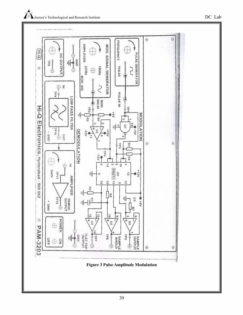
Figure 3 Pulse Amplitude Modulation
Auroras Technological and Research Institute AC Lab
Department of ECE 5
EXPERIMENT NO 11
PULSE WIDTH MODULATION AND DEMODULATION
AIM
1) To study the PWM process and the corresponding waveforms 2) To study the effect of sampling frequency on the transmission of information through PWM
PRE LAB WORK
Study the operation Pulse Width Modulator and Demodulator Draw the block diagram of PWM modulator and demodulator Draw the expected graphs of all necessary waveforms ( message signal carrier wave PWM op
demodulated op etc
EQUIPMENT
1) Experimental Board
2) Dual trace CRO 3) AF generator 4) Multimeter
THEORY
In PWM the samples of the message signal are used to vary the duration of the individual pulses The
pulse width may be varied by varying the time of occurrence of the leading edge trailing edge of both
edges of the pulse in accordance with the sampled value of the modulating wave PWM can also be
generated by using emitter follower monostable multivibrator is an excellent voltage to time converter
since its gate width is dependent on the voltage to which the capacitor is changed If this voltage can be
varied in accordance with a signal voltage a series of rectangular pulses can be obtained with width
varying as required
The demodulated of PWM is quite simple PWM is passed through a low pass filter The reconstruction is
associated with a certain amount of Distortion caused by the cross modulator products that fall in the
signal band
EXPECTED WAVEFORM
Aurorarsquos Technological and Research Institute DC Lab
41
PROCEDURE
STUDY OF MODULATION
1) Observe the clock on CRO and measure its frequency (fs) 2) Observe the sine wave modulating signal on CRO and observe the dc shift produced in this
by varying the offset nob Measure the frequency Variation limits of this signal 3) Apply clock at the circuit input terminal 4) Apply modulating signal by keeping the control switch in dc position 5) Observe the modulated wave 6) Plot the graph bw pulse width and the applied dc voltage 7) Put the control switch in sine wave position and adjust the modulating signal amplitude
frequency and dc offset to get the stationary waveform of PWM 8) Note the number of pulses in one circuit of modulating signal
STUDY OF DEMODULATION
1) Generate the stationary PWM waveform using sin wave modulating signal 2) Connect the modulator OP to PWM demodulator 3) Connect Channel (1) to Modulating Signal and channel (2) to demodulated wave
EFFECT OF SAMPLING FREQUENCY
1) Use an external square wave and connect it to the clock input 2) Set the frequency of square wave at frequency 2fm 3) Observe the demodulated wave
4) Change the frequency of square wave to fs lt 2fm fs gt 2fm and observe the demodulated wave
RESULT
CONCLUSION
Aurorarsquos Technological and Research Institute DC Lab
42
Figure 4 Pulse Width Modulation
Aurorarsquos Technological and Research Institute DC Lab
43
EXPERIMENT NO 12
PULSE POSITION MODULATION AND DEMODULATION
AIM
1) To study the PPM Modulation and the corresponding waveforms 2) To study the de-modulation of PPM 3) To see the effect of sampling frequency on the transmission of information through PPM
PRE LAB WORK
Study the operation Pulse Position Modulator and Demodulator Draw the block diagram of PPM modulator and demodulator Draw the expected graphs of all necessary waveforms ( message signal carrier wave PPM op
demodulated op etc
EQUIPMENT
1) Experimental Board for PPM
2) Dual Phase Oscilloscope
3) AF Generator
THEORY
In PDM long pulses expand considerable power duration If the pulse which bearing no additional
information If this un used power is subtracted from PDM so that only time transitions are preserved
We observe a more efficient type of pulse modulation known as pulse position modulation Here in the
Pulse Position Modulated wave the position of the Pulse relative to its unmodulated time of occurrence is
varied in accordance with the message signal
We generate a PPM wave from PWM wave by using a Monostable Multivibrator The device has one
absolutely stable state and one quest ndash stable state into which it is triggered by an externally applied Pulse
The monostable multivibrator is designed to trigger on the trailing edges of the duration ndash modulated pulse
is varied in accordance with the message signal
The fixed pulse duration of the PPM wave at the monostable multivibrator OP can be set by appropriately
choosing the resistance ndash capacitance combination in the timing circuit of the device
Aurorarsquos Technological and Research Institute DC Lab
44
EXPECTED WAVEFORM
PROCEDURE
STUDY OF MODULATION
Observe the clock and measure its frequency (fs) Apply the clock at the clock IP terminal in the modulator Apply the modulating signal keeping control switch in DC position Observe the PPM OP Connect the channel ndash (1) on CRO to clock and channel (2) to PPM wave OP Compare the position of two waveforms Vary the DC offset and observe the relative shift between the clock and PPM OP Measure the time shift between clock and PPM wave for various settings of offset Draw the graph between time shift and DC voltage Put the control switch in AC position adjusts the amplitude and frequency and offset
of sinusoidal modulating signal to get the stationary PPM wave Note the number of pulses in one cycle of the modulated wave
STUDY OF DEMODULATION
Generate a stationery PPM wave for a sinusoidal modulating signal Apply the PPM wave to the input of de-modulator Connect the Channel ndash (1) of CRO to the modulating signal and channel ndash 2 to the
de-modulator output Compare the two waveforms
Note the frequency of demodulated wave It should be same as the modulating signal Note down the waveform
RESULT
CONCLUSION
Aurorarsquos Technological and Research Institute DC Lab
45
Aurorarsquos Technological and Research Institute DC Lab
46
Figure 5 Pulse Position Modulation
Aurorarsquos Technological and Research Institute AC Lab
47
EXPERIMENT NO 13
FREQUENCY SYNTHESIZER
AIM
To study the operation of frequency synthesizer using PLL
PRE-LAB 1 Study the data sheet of IC 7404IC 4017IC 565 and IC 4046
2 Study the theory of frequency synthesizer 3 Draw the circuit diagram and expected waveforms
EQUIPMENTS
1 Frequency synthesizer trainer AET -26A
2 Dual trace CRO (20Mhz) 3 Digital frequency counter or multimeter
4 Patch chords
THEORY
A frequency synthesizer is an electronic system for generating any of a range
of frequencies from a single fixed time base or oscillator They are found in many modern
devices including radio receivers mobile telephones radiotelephones walkie-talkies CB
radios satellite receivers GPS systems etc A frequency synthesizer can combine
frequency multiplication frequency division and frequency mixing (the frequency mixing
process generates sum and difference frequencies) operations to produce the desired output
signal
BLOCK DIAGRAM
Phase Comparator
Amplifier Low pass filter
V C O
Div N Network frequency divider
Fin= fout
N
fin
Fout =Nf in
Aurorarsquos Technological and Research Institute AC Lab
48
SIMPLE 1KHZ-9KHZ FREQUENCY SYNTHESIZER
CIRCUIT DAIGRAM
PROCEDURE 1 Switch on the trainer ad verify the output of the regulated power supply ie 5V These
supplied are internally connected to the circuit so no extra connections are required 2 Observe output of the square wave generator using oscilloscope and measure the range
with the help of frequency counter frequency range should be around 1KHz to 10KHz 3 Calculate the free running frequency range of the circuit (VCO output between 4th pin
and ground 1 For different values of timing resistor R1 ( to measure Rt value using digital multimeter between given test points 1 And record the frequency values in table 1
Fout = 03 (RtCt) where Rt is the timing resistor and Ct is the timing capacitor = 001 f
Aurorarsquos Technological and Research Institute AC Lab
49
4 Connect 4th pin of LM 565 (Fout) to the driver stage and 5th pin (Phase comparator) connected to 11th pin of 7404 Output can be taken at the 11th pin of the 7490 It should be divided by the 2 amp 3 times of the fout
TABULATION
Fin KHz Fout = N x fin KHz Divided by 3 2
EXPECTED WAVEFORMS
POST LAB
1 Observe the synthesized output in table 2 Calculate the output frequency
3 Plot the output waveforms
4 Write result and conclusions
CONCLUSIONS
The various outputs of frequency synthesizer are verified
QUESTIONS
1 What are the applications of frequency synthesizer
TIME T
A
m
p
l i T
u
d
e
Ac
Aurorarsquos Technological and Research Institute AC Lab
50
2 What is the difference between heterodyning and synthesizer
Aurorarsquos Technological and Research Institute AC Lab
51
EXPERIMENT NO 14
AGC CHARATERISTICS
AIM
To observe the effect of automatic gain control(AGC)
PRE LAB 1 To study the theory of AGC 2 Draw the Block Diagram circuits diagram and expected waveforms
EQUIPMENTS 1 AGC Trainer Kit 2 CRO
3 Patch Chords
4 Digital Multimeter
THEORY
Automatic gain control (AGC) is an adaptive system found in many electronic
devices The average output signal level is fed back to adjust the gain to an appropriate level
for a range of input signal levels For example without AGC the sound emitted from an AM
radio receiver would vary to an extreme extent from a weak to a strong signal the AGC
effectively reduces the volume if the signal is strong and raises it when it is weaker AGC
algorithms often use a PID controller where the P term is driven by the error between
expected and actual output amplitude
Block Diagram
Frequency Converter
1st IF Amplifier
2nd IF Amplifier
Detector
Audio Preamplifier
Driver Output
Aurorarsquos Technological and Research Institute AC Lab
52
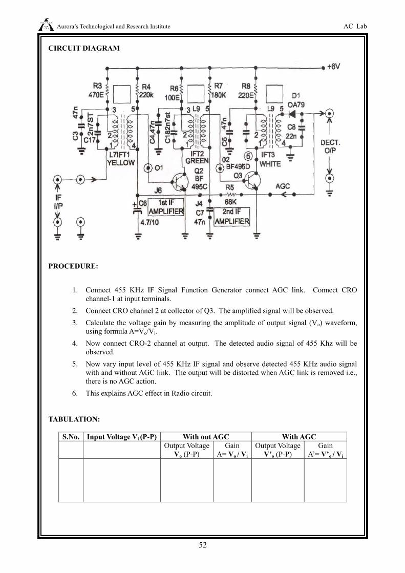
CIRCUIT DIAGRAM
PROCEDURE
1 Connect 455 KHz IF Signal Function Generator connect AGC link Connect CRO channel-1 at input terminals
2 Connect CRO channel 2 at collector of Q3 The amplified signal will be observed 3 Calculate the voltage gain by measuring the amplitude of output signal (Vo) waveform
using formula A=VoVi 4 Now connect CRO-2 channel at output The detected audio signal of 455 Khz will be
observed 5 Now vary input level of 455 KHz IF signal and observe detected 455 KHz audio signal
with and without AGC link The output will be distorted when AGC link is removed ie there is no AGC action
6 This explains AGC effect in Radio circuit
TABULATION
SNo Input Voltage Vi (P-P) With out AGC With AGC
Output Voltage Vo (P-P)
Gain A= Vo Vi
Output Voltage Vrsquoo (P-P)
Gain Arsquo= Vrsquoo Vi
Aurorarsquos Technological and Research Institute AC Lab
53
EXPECTED WAVEFORMS
AM Modulated RF Input
Detected Output with AGC
Detected Output without AGC
POST-LAB
1 Observe the input voltage and output voltage for with AGC and Without AGC in Table 1
2 Calculate Gain a=vovi for both cases 3 Plot the output waveforms Time T Vs Voltage Vo and input voltage Vi Vs Gain A 4 Write Result and Conclusions
CONCLUSIONS The AGC characteristics are verified
QUESTIONS 1 what is meant by AGC
2 What is the difference between simple AGC and delayed AGC
3 From which part of receiver AGC is obtained
TIME T
A
m
p
l i T
u
d
e
Ac
TIME T
A
m
p
l i T
u
d
e
Ac
TIME T
A
m
p
l i T
u
d
e
Ac
Aurorarsquos Technological and Research Institute AC Lab
54
EXPERIMENT NO 15
PHASE LOCKED LOOP
OBJECTIVE To study the Phase locked loop using 565 IC and to take input frequency given by an external signal source
PRE-LAB To Study
1 The data sheet of IC 565
2 The theory of Phase locked loop
3 About free running frequency locking range and capture range
4 Draw the circuit diagram and expected waveforms
EQUIPMENT 1 Function generator 2
2 Dual trace CRO 1
3 Phase locked loop trainer kit
THEORY
A phase-locked loop or phase lock loop (PLL) is a control system that generates a signal
that has a fixed relation to the phase of a reference signal A phase-locked loop circuit
responds to both the frequency and the phase of the input signals automatically raising or
lowering the frequency of a controlled oscillator until it is matched to the reference in both
frequency and phase A phase-locked loop is an example of a control system using negative
feedback Phase-locked loops are widely used in radio telecommunications computers and
other electronic applications They may generate stable frequencies recover a signal from a
noisy communication channel or distribute clock timing pulses in digital logic designs
such as microprocessors Since a single integrated circuit can provide a complete phase-
locked-loop building block the technique is widely used in modern electronic devices
with output frequencies from a fraction of a cycle per second up to many gigahertz
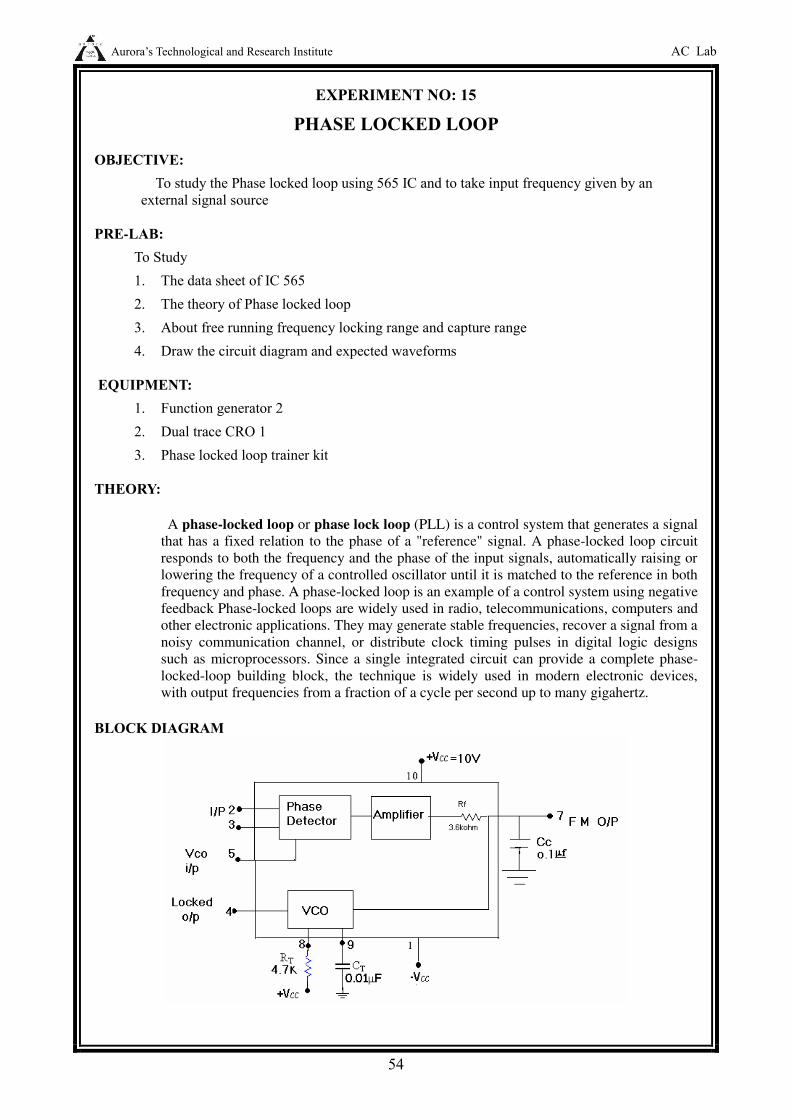
BLOCK DIAGRAM
Aurorarsquos Technological and Research Institute AC Lab
55
CIRCUIT DIAGRAM
PROCEDURE 1 Switch ON the trainer kit 2 Check the VCO output at pin 4 of IC 565 that is a square wave form The frequency of the
VCO Output depends on CT (001f) and RT (47kΩ) 3 Next short the pins 4amp5 and give signal of variable frequency and observe VCO output 4 Change the input frequency and observe the VCO output on the CRO 5 Between some frequencies the VCO output is locked to the input signal frequency This can
be observed by increasing or decreasing the frequency of the VCO output by changing input frequency
6 Before or after that frequency range the VCO output is not locked
7 Calculate Lock range (FL) and capture range (FC) by using the following formulas
FL = 8foVCO fo=03RtCT
FC=12π radic2πf236103 C2
Table1
SNo Locking Frequency Frequency Range From To
CHARTERISTICES
Aurorarsquos Technological and Research Institute AC Lab
56
CONCLUSIONS Obtained the lock range of PLL
QUESTIONS
1 Observe the VCO output when pins 4amp5 short and give square wave as signal 2 Define lock range and capture range
3 What are the basic applications of PLL
Aurorarsquos Technological and Research Institute AC Lab
57
ANNEXURE-I
EXPERIMENT NO 1
Aurorarsquos Technological and Research Institute AC Lab
58
CHARACTERISTICS OF MIXER
AIM
To study the functioning of a frequency mixer
PRE LAB 1 To study the theory of Mixer 2 Draw the circuit diagram and expected waveforms
EQUIPMENTS 1 Frequency mixer trainer kit 2 CRO (20MHz) 3 Connecting cords and probes 4 Function generator (1MHz)
THEORY
In receivers using the super heterodyne principle a signal at variable frequency is
converted to a fixed lower frequency IF before detection IF is called the intermediate frequency
In typical AM (Amplitude Modulation eg as used on medium wave) home receivers that
frequency is usually 455 kHz for FM VHF receivers it is usually 107 MHz An intermediate
frequency (IF) is a frequency to which a carrier frequency is shifted as an intermediate step in
transmission or reception Frequency modulation (FM) is a form of modulation that represents
information as variations in the instantaneous frequency of a carrier wave Very high frequency
(VHF) is the radio frequency range from 30 MHz (wavelength 10 m) to 300 MHz (wavelength 1
heterodyne receivers mix all of the incoming signals with an internally generated waveform
called the local oscillator The user tunes the radio by adjusting the sets oscillator frequency in
the mixer stage of a receiver the local oscillator signal multiplies with the incoming signals
which shifts them all down in frequency The one that shifts is passed on by tuned circuits
amplified and then demodulated to recover the original audio signal The oscillator also shifts a
copy of each incoming signal up in frequency by amount Those very high frequency images
are all rejected by the tuned circuits in the IF stage The Super heterodyne receiver (or to give it its
full name The Supersonic Heterodyne Receiver usually these days shortened to superhet) was
invented by Edwin Armstrong in 1918
Aurorarsquos Technological and Research Institute AC Lab
59
BLOCK DIAGRAM
CIRCUIT DIAGRAM
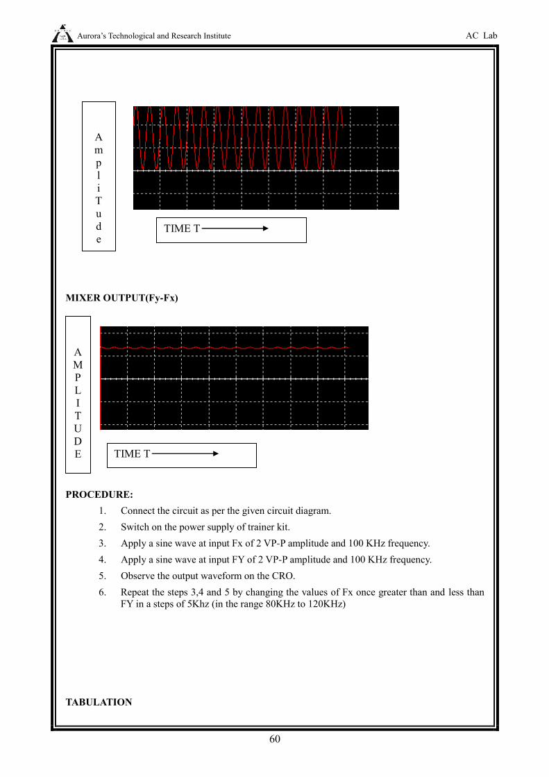
EXPECTED WAVEFORMS
INPUT SIGNAL Fx
INPUT SIGNAL Fy
TIME T
A
m
p
l i T
u
d
e
Ac
Aurorarsquos Technological and Research Institute AC Lab
60
MIXER OUTPUT(Fy-Fx)
PROCEDURE 1 Connect the circuit as per the given circuit diagram 2 Switch on the power supply of trainer kit 3 Apply a sine wave at input Fx of 2 VP-P amplitude and 100 KHz frequency 4 Apply a sine wave at input FY of 2 VP-P amplitude and 100 KHz frequency 5 Observe the output waveform on the CRO 6 Repeat the steps 34 and 5 by changing the values of Fx once greater than and less than
FY in a steps of 5Khz (in the range 80KHz to 120KHz)
TABULATION
TIME T
A
M
P
L
I T
U
D
E
TIME T
A
m
p
l i T
u
d
e
Ac
Aurorarsquos Technological and Research Institute AC Lab
61
SNo Freq (Fy)
(kHz) Amp(V) Freq(Fx) (kHz) Amp(V) Freq(Fy-Fx)
(kHz) Amp(V)
POST LAB 1 Observe the amplitude and time Of inputs and output in table
2 Draw the expected waveforms
3 Verify the output signal obtained with the theoretical value 4 Plot the graphs for Time T VS input signal (FX) Voltage V input signal (FY) Voltage V
and output Signal F(x-y) voltage V 5 Write result and conclusions
CONCLUSIONS
Obtained the output of the mixer for various inputs
QUESTIONS
1 what are the different types of mixtures available
2 What is meant by heterodyning
3 What is meant by IF
Aurorarsquos Technological and Research Institute AC Lab
62
EXPERIMENT NO 2
DIGITAL PHASE DETECTOR
OBJECTIVE To detect the phase difference between two square wave signals using digital phase detector
PRE LAB
1 To study the theory of digital phase detector and EX-OR gate operation and truth table 2 Draw the circuit diagram and expected output and input waveforms
EQUIPMENT 1 Digital phase detector trainer kit 2 Regulated power supplies
3 CRO (20MHz) 4 Connecting cords amp probes
5 Digital frequency counter or multimeter
THEORY
Phase detector is a frequency mixer or analog multiplier circuit that generates a voltage
signal which represents the difference in phase between two signal inputs It is an essential
element of the phase-locked loop (PLL)Detecting phase differences is very important in many
applications such as motor control radar and telecommunication systems servo mechanisms and
demodulators
Electronic phase detector
Some signal processing techniques such as those used in radar may require both the amplitude
and the phase of a signal to recover all the information encoded in that signal One technique is to
feed an amplitude-limited signal into one port of a product detector and a reference signal into the
other port the output of the detector will represent the phase difference between the signals If the
signal is different in frequency from the reference the detector output will be periodic at the
difference frequency Phase detectors for phase-locked loop circuits may be classified in two
types A Type I detector is designed to be driven by analog signals or square-wave digital signals
and produces an output pulse at the difference frequency The Type I detector always produces an
output waveform which must be filtered to control the phase-locked loop variable frequency
oscillator (VCO) A type II detector is sensitive only to the relative timing of the edges of the input
and reference pulses and produces a constant output proportional to phase difference when both
signals are at the same frequency This output will tend not to produce ripple in the control voltage
of the VCO
Aurorarsquos Technological and Research Institute AC Lab
63
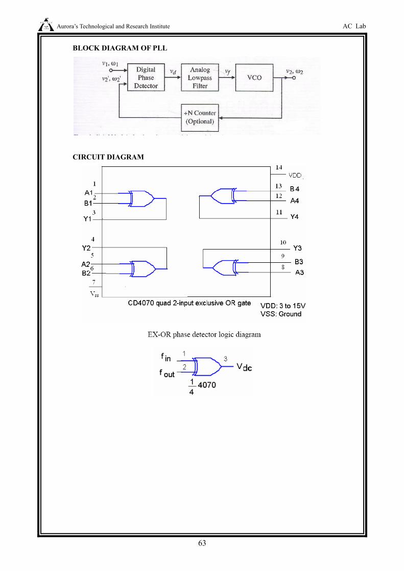
BLOCK DIAGRAM OF PLL
CIRCUIT DIAGRAM
Aurorarsquos Technological and Research Institute AC Lab
64
EXPECTED WAVEFORMS
EX-OR PHASE DETECTOR
EDGE TRIGGERED OUTPUT
PROCEDURE
1 Switch on the trainer kit
2 Observe the output of the square wave generator available on the trainer kit using CRO
and measure the range with the help of frequency counter the frequency range should be
around 2 KHz to 13 KHz
3 Calculate the free running range of the VCO output ie between 4th pin of IC PLL 565
and ground For different values of timing resistor Rt fout is given by Fout =03 Rt Ct
where Ct timing capacitor = 001 μF Rt timing resistor
4 Connect the square wave to the input of IC PLL 565 and short 4th and 5th pin of PLL
Vary the input frequency of the square wave when the PLL is locked that is connected to
Aurorarsquos Technological and Research Institute AC Lab
65
one input fout EX-OR phase detector The other input fin of EX-OR phase detector is the
coming from inbuilt of square wave generator
5 Connect the pulse generator output to the input of IC 565 PLL and short 4th amp 5th pin of
PLL Vary the input frequency of the square wave when the PLL is locked that is
connected to one input of Edge triggered phase detector input ie fout The other input fin
of edge triggered phase detector is the pulse input coming from the inbuilt pulse generator
6 The dc output voltage of the exclusive-OR phase detector is a function of the phase
difference between its two inputs fin and fout
POST LAB
1 Observe the Voltage and Time of the two input square waves
2 Observe difference of two inputs as square wave output
3 Plot the inputs and output waveforms Time T VS Voltage V
CONCLUSIONS
The phase detector outputs are verified
QUESTIONS
1 What is the function of phase detector
2 What is the condition for getting maximum output
3 Advantages of digital phase detector over analog phase detector
Aurorarsquos Technological and Research Institute AC Lab
66
EXPERIMENT NO 3
COASTAS RECEIVER
AIM
To demodulate a DSB-SC signal using coastas receiver
PRE LAB 1 To study the operation of coastas receiver 2 Draw the circuit diagram and expected waveforms
EQUIPMENTS 1 Communications trainer kit 2 DSB-SC modulator trainer kit 3 CRO (20MHz) 4 Connecting cords and probes 5 Function generator (1MHz)
THEORY
This loop and its variations is much-used as a method of carrier acquisition (and
simultaneous message demodulation) in communication systems both analog and digital
It has the property of being able to derive a carrier from the received signal even when there is
no component at carrier frequency present in that signal (eg DSBSC) The requirement is that
the amplitude spectrum of the received signal be symmetrical about this frequency
The Costas loop is based on a pair of quadrature modulators - two multipliers
fed with carriers in phase-quadrature These multipliers are in the in-phase (I) and quadrature
phase (Q) arms of the arrangement Each of these multipliers is part of separate synchronous
demodulators The outputs of the modulators after filtering are multiplied together in a third
multiplier and the lowpass components in this product are used to adjust the phase of the local
carrier source - a VCO - with respect to the received signal The operation is such as to
maximise the output of the I arm and minimize that from the Q arm The output of the I arm
happens to be the message and so the Costas loop not only acquires the carrier but is a
(synchronous) demodulator as well A complete analysis of this loop is non-trivial It would
include the determination of conditions for stability and parameters such as lock range capture
range and so on
Aurorarsquos Technological and Research Institute AC Lab
67
BLOCK DIAGRAM
EXPECTED WAVEFORMS
DSB-SC modulated output
Aurorarsquos Technological and Research Institute AC Lab
68
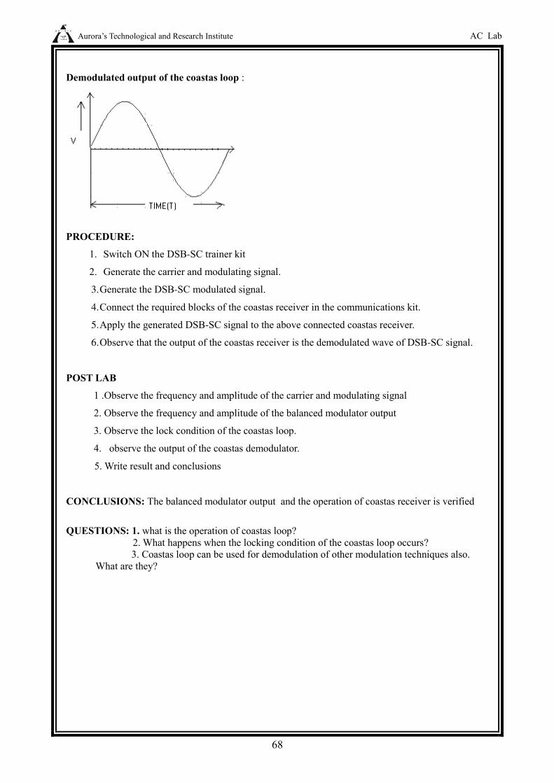
Demodulated output of the coastas loop
PROCEDURE
1 Switch ON the DSB-SC trainer kit
2 Generate the carrier and modulating signal
3 Generate the DSB-SC modulated signal
4 Connect the required blocks of the coastas receiver in the communications kit
5 Apply the generated DSB-SC signal to the above connected coastas receiver
6 Observe that the output of the coastas receiver is the demodulated wave of DSB-SC signal
POST LAB
1 Observe the frequency and amplitude of the carrier and modulating signal
2 Observe the frequency and amplitude of the balanced modulator output
3 Observe the lock condition of the coastas loop
4 observe the output of the coastas demodulator
5 Write result and conclusions
CONCLUSIONS The balanced modulator output and the operation of coastas receiver is verified
QUESTIONS 1 what is the operation of coastas loop
2 What happens when the locking condition of the coastas loop occurs
3 Coastas loop can be used for demodulation of other modulation techniques also What are they
Aurorarsquos Technological and Research Institute AC Lab
69
MATLAB PROGRAMMES
Aurorarsquos Technological and Research Institute AC Lab
70
INDEX
1 Introduction - 70
2 Amplitude Modulation and Demodulation - 74
3 DSB-SC Modulation and Demodulation - 84
4 SSB-SC Modulation and Demodulation - 89
5 Frequency Modulation and Demodulation - 95
6 Phase Modulation and Demodulation - 99
7 Time Division Multiplexing and Demultiplexing - 100
8 Frequency Division Multiplexing and Demultiplexing- 103
9 Verification of Sampling Theorem - 104
10 Pulse Amplitude Modulation and Demodulation - 106
11 Pulse width Modulation and Demodulation - 108
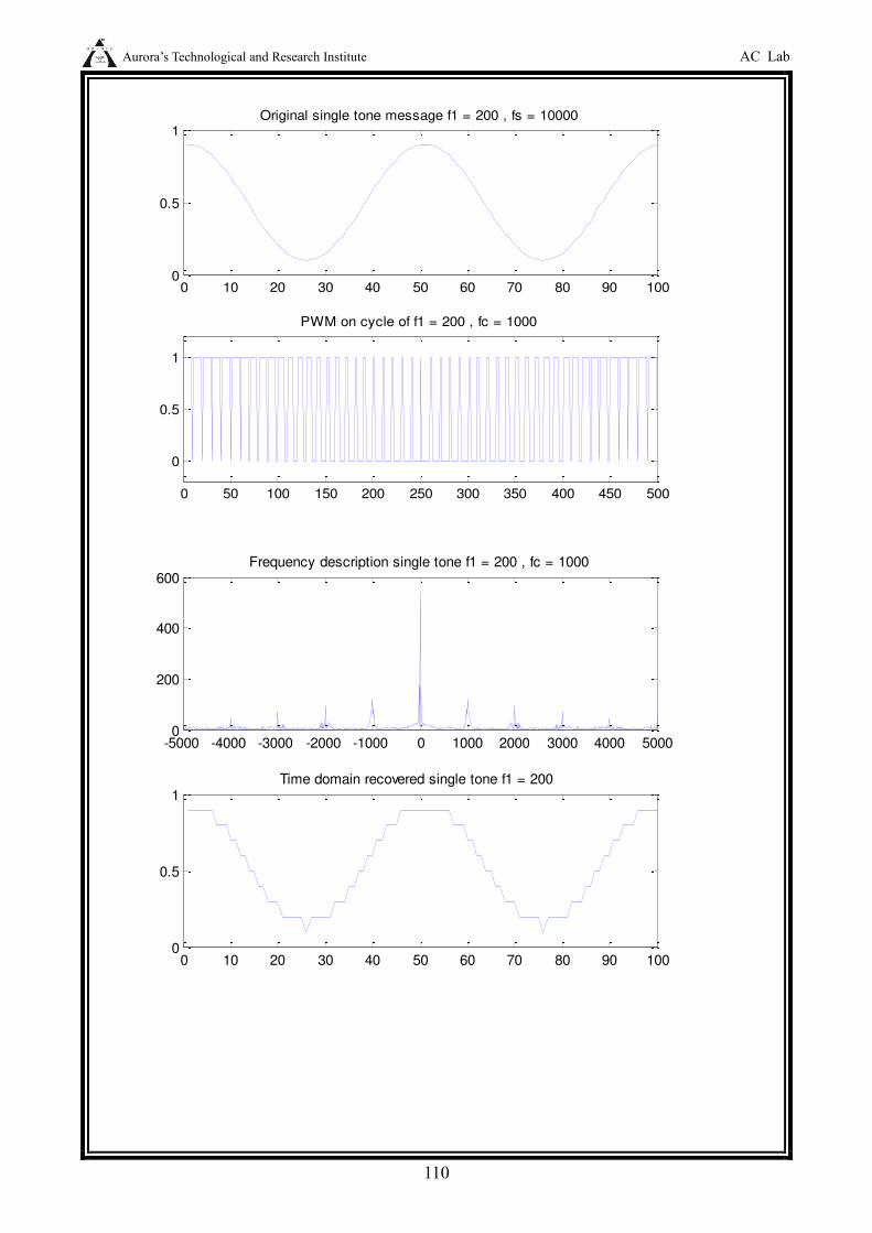
12 Pulse Position Modulation and Demodulation - 110
13 PLL as FM Demodulator - 112
Aurorarsquos Technological and Research Institute AC Lab
71
1 INTRODUCTION
What Is Simulink
Simulink is a software package for modeling simulating and analyzing dynamic
systems It supports linear and nonlinear systems modeled in continuous time sampled time
or a hybrid of the two Systems can also be multirate ie have different parts that are
sampled or updated at different rates
Tool for Simulation
Simulink encourages you to try things out You can easily build models from scratch
or take an existing model and add to it You have instant access to all the analysis tools in
MATLABreg so you can take the results and analyze and visualize them A goal of Simulink
is to give you a sense of the fun of modeling and simulation through an environment that
encourages you to pose a question model it and see what happens
Simulink is also practical With thousands of engineers around the world using it to
model and solve real problems knowledge of this tool will serve you well throughout your
professional career
Tool for Model-Based Design
With Simulink you can move beyond idealized linear models to explore more realistic
nonlinear models factoring in friction air resistance gear slippage hard stops and the other
things that describe real-world phenomena Simulink turns your computer into a lab for
modeling and analyzing systems that simply wouldnt be possible or practical otherwise
whether the behavior of an automotive clutch system the flutter of an airplane wing the
dynamics of a predator-prey model or the effect of the monetary supply on the economy
For modeling Simulink provides a graphical user interface (GUI) for building models
as block diagrams using click-and-drag mouse operations With this interface you can draw
the models just as you would with pencil and paper (or as most textbooks depict them) This
is a far cry from previous simulation packages that require you to formulate differential
equations and difference equations in a language or program Simulink includes a
comprehensive block library of sinks sources linear and nonlinear components and
connectors You can also customize and create your own blocks For information on creating
your own blocks see the separate Writing S-Functions guide
Models are hierarchical so you can build models using both top-down and bottom-up
approaches You can view the system at a high level then double-click blocks to go down
through the levels to see increasing levels of model detail This approach provides insight into
how a model is organized and how its parts interact
After you define a model you can simulate it using a choice of integration methods either
from the Simulink menus or by entering commands in the MATLAB Command Window The
menus are particularly convenient for interactive work while the command-line approach is
very useful for running a batch of simulations (for example if you are doing Monte Carlo
simulations or want to sweep a parameter across a range of values) Using scopes and other
display blocks you can see the simulation results while the simulation is running In addition
Aurorarsquos Technological and Research Institute AC Lab
72
you can change many parameters and see what happens for what if exploration The
simulation results can be put in the MATLAB workspace for post processing and
visualization
Model analysis tools include linearization and trimming tools which can be accessed
from the MATLAB command line plus the many tools in MATLAB and its application
toolboxes And because MATLAB and Simulink are integrated you can simulate analyze
and revise your models in either environment at any point
1 Generation of cosine wave in time domain and frequency
domain Clc clear all close all x = -500015 t = 0140001 time = cos(23141000t) y1 = cos(23141000x) subplot(211) plot(xy1) axis([-5 5 -3 3]) grid on title(Time domain) xlabel(Time ) ylabel(Amplitude) now create a frequency vector for the x-axis and plot the magnitude and phase subplot(212) fre = abs(fft(time)) f = (0length(fre) - 1)4000length(fre) plot(ffre) grid on title(Frequency domain (Spectrum)) xlabel(Freq ) ylabel(Amplitude)
WAVEFORMS
Aurorarsquos Technological and Research Institute AC Lab
73
2 Generation of square wave in time domain and frequency
domain
clc clear all close all x = -500015 Fs = 399 t = 01Fs1 time = SQUARE(2pi1000t) y1 = SQUARE(23141000x) subplot(211) plot(xy1) axis([-5 5 -3 3]) grid on xlabel(Time domain) ylabel(Amplitude) now create a frequency vector for the x-axis and plot the magnitude and phase subplot(212) fre = abs(fft(time)) f = (0length(fre) - 1)Fslength(fre) plot(ffre) grid on xlabel(Freq domain) ylabel(Amplitude)
WAVEFORMS
Aurorarsquos Technological and Research Institute AC Lab
74
Aurorarsquos Technological and Research Institute AC Lab
75
2 AMPLITUDE MODULATION AND DEMODULATION PROGRAM 1
clc clear all close all Ac=1 Carrier Amplitude Fc=04 Carrier frequency Fm=005 baseband frequency Fs=10 sampling t=001200 mt=cos(2piFmt) under modulation mu=05 st=Ac(1+mumt)cos(2piFct) subplot(211) plot(tst) hold on plot(tAc(mumt+ones(1length(mt)))r) plot(t-Ac(mumt+ones(1length(mt)))r) hold off title(Modulation Index = 05 under modulation Ac(1+05cos(2pi005t))cos(2pi04t)) xlabel(time (s))ylabel(amplitude) st_fft=fft(st) st_fft=fftshift(st_fft) st_fft_fre=5linspace(-11length(st_fft)) subplot(212) plot(st_fft_freabs(st_fft)) title(spectrum with Modulation Index = 05) xlabel(Frequency (Hz))axis([-1 1 0 1000Ac+100])
total modulation figure mu=1 st=Ac(1+mumt)cos(2piFct) subplot(211) plot(tst) hold on plot(tAc(mumt+ones(1length(mt)))r) plot(t-Ac(mumt+ones(1length(mt)))r) hold off title(Modulation Index = 1 modulation Ac(1+1cos(2pi005t))cos(2pi04t)) xlabel(time (s))ylabel(amplitude) st_fft=fft(st) st_fft=fftshift(st_fft) st_fft_fre=Fs2linspace(-11length(st_fft)) subplot(212) plot(st_fft_freabs(st_fft)) title(spectrum with Modulation Index = 1) xlabel(Frequency (Hz))axis([-1 1 0 1000Ac+100])
Aurorarsquos Technological and Research Institute AC Lab
76
over Modulation figure mu=2 st=Ac(1+mumt)cos(2piFct) subplot(211) plot(tst) hold on plot(tAc(mumt+ones(1length(mt)))r) plot(t-Ac(mumt+ones(1length(mt)))r) hold offtitle(Modulation Index = 2 over modulation Ac(1+2cos(2pi005t))cos(2pi04t)) xlabel(time (s))ylabel(amplitude) st_fft=fft(st) st_fft=fftshift(st_fft) st_fft_fre=Fs2linspace(-11length(st_fft)) subplot(212) plot(st_fft_freabs(st_fft)) title(spectrum with Modulation Index = 2) xlabel(Frequency (Hz))axis([-1 1 0 1000Ac+100])
WAVEFORMS
Aurorarsquos Technological and Research Institute AC Lab
77
PROGRAM 2
Aurorarsquos Technological and Research Institute AC Lab
78
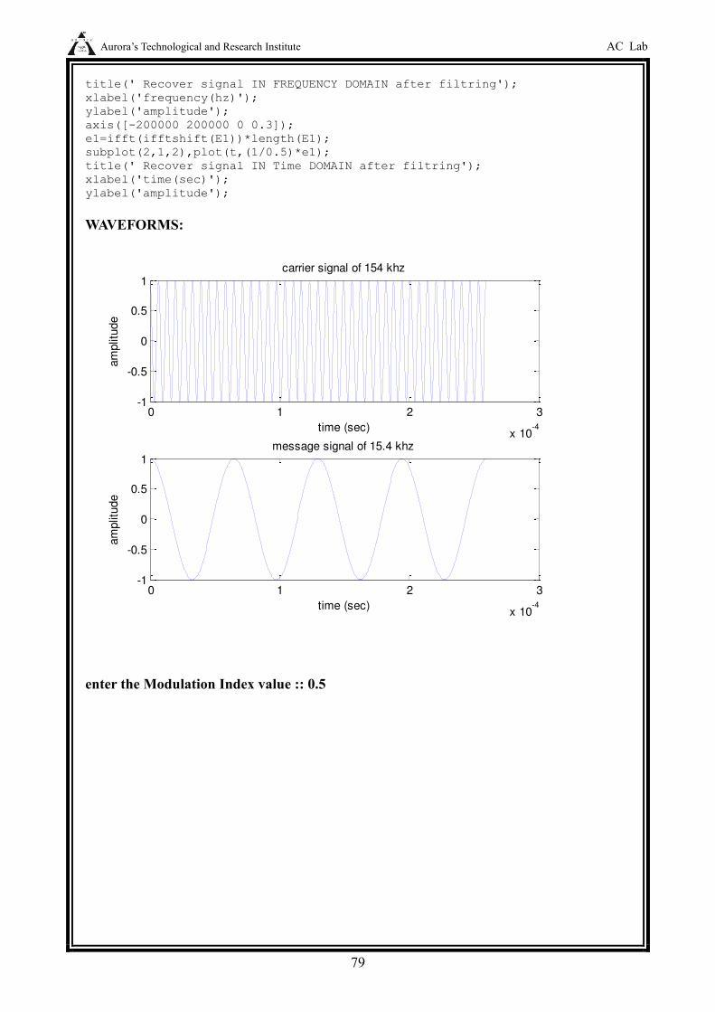
task 1 fc=154000
task 2 fm=fc10 fs=100fc t=01fs4fm xc=cos(2pifct) xm=cos(2pifmt) figure(1) subplot(211)plot(txc) title(carrier signal of 154 khz) xlabel(time (sec)) ylabel(amplitude) subplot(212)plot(txm) title(message signal of 154 khz) xlabel(time (sec)) ylabel(amplitude) DSB-SC MODULATION mu = input( enter the Modulation Index value ) z1=(1+muxm)xc figure(2)
task 31 subplot(211)plot(tz1) title(AMPLITUDE MODULATION IN TIME DAOMAIN) xlabel(time (sec)) ylabel(amplitude)
task 32 l1=length(z1) f=linspace(-fs2fs2l1) Z1=fftshift(fft(z1l1)l1) subplot(212)plot(fabs(Z1)) title(AMPLITUDE MODULATION IN FREQUENCY DOMAIN) xlabel(frequency(hz)) ylabel(amplitude) axis([-200000 200000 0 03])
task 33 demodulation s1=z1xc S1=fftshift(fft(s1length(s1))length(s1)) figure(3) plot(fabs(S1)) title( demodulated signal IN FREQUENCY DOMAIN before filtring) xlabel(frequency(hz)) ylabel(amplitude) axis([-200000 200000 0 03]) hold on Hlp=1sqrt(1+(ffc)^(2100)) plot(fHlpr) title( frequency response of low pass filter) xlabel(frequency(hz)) ylabel(amplitude) axis([-200000 200000 0 2])
task 34 E1=HlpS1 figure(4) subplot(211)plot(fE1)
Aurorarsquos Technological and Research Institute AC Lab
79
title( Recover signal IN FREQUENCY DOMAIN after filtring) xlabel(frequency(hz)) ylabel(amplitude) axis([-200000 200000 0 03]) e1=ifft(ifftshift(E1))length(E1) subplot(212)plot(t(105)e1) title( Recover signal IN Time DOMAIN after filtring) xlabel(time(sec)) ylabel(amplitude)
WAVEFORMS
enter the Modulation Index value 05
0 1 2 3
x 10-4
-1
-05
0
05
1carrier signal of 154 khz
time (sec)
am
plit
ude
0 1 2 3
x 10-4
-1
-05
0
05
1message signal of 154 khz
time (sec)
am
plit
ude
Aurorarsquos Technological and Research Institute AC Lab
80
0 1 2 3
x 10-4
-2
-1
0
1
2AMPLITUDE MODULATION IN TIME DAOMAIN
time (sec)
am
plit
ude
-2 -15 -1 -05 0 05 1 15 2
x 105
0
01
02
AMPLITUDE MODULATION IN FREQUENCY DOMAIN
frequency(hz)
am
plit
ude
-2 -15 -1 -05 0 05 1 15 2
x 105
0
02
04
06
08
1
12
14
16
18
2 frequency response of low pass filter
frequency(hz)
am
plit
ude
Aurorarsquos Technological and Research Institute AC Lab
81
enter the Modulation Index value 1
-2 -15 -1 -05 0 05 1 15 2
x 105
0
01
02
Recover signal IN FREQUENCY DOMAIN after filtring
frequency(hz)
am
plit
ude
0 1 2 3
x 10-4
05
1
15
2 Recover signal IN Time DOMAIN after filtring
time(sec)
am
plit
ude
0 1 2 3
x 10-4
-2
-1
0
1
2AMPLITUDE MODULATION IN TIME DAOMAIN
time (sec)
am
plit
ude
-2 -15 -1 -05 0 05 1 15 2
x 105
0
01
02
AMPLITUDE MODULATION IN FREQUENCY DOMAIN
frequency(hz)
am
plit
ude
Aurorarsquos Technological and Research Institute AC Lab
82
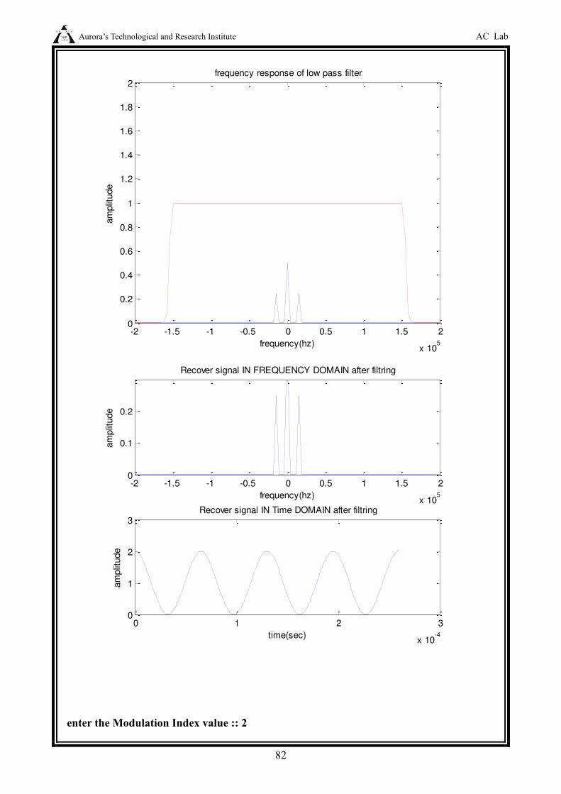
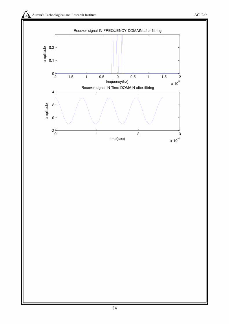
enter the Modulation Index value 2
-2 -15 -1 -05 0 05 1 15 2
x 105
0
02
04
06
08
1
12
14
16
18
2 frequency response of low pass filter
frequency(hz)
am
plit
ude
-2 -15 -1 -05 0 05 1 15 2
x 105
0
01
02
Recover signal IN FREQUENCY DOMAIN after filtring
frequency(hz)
am
plit
ude
0 1 2 3
x 10-4
0
1
2
3 Recover signal IN Time DOMAIN after filtring
time(sec)
am
plit
ude
Aurorarsquos Technological and Research Institute AC Lab
83
0 1 2 3
x 10-4
-4
-2
0
2
4AMPLITUDE MODULATION IN TIME DAOMAIN
time (sec)
am
plit
ude
-2 -15 -1 -05 0 05 1 15 2
x 105
0
01
02
AMPLITUDE MODULATION IN FREQUENCY DOMAIN
frequency(hz)
am
plit
ude
-2 -15 -1 -05 0 05 1 15 2
x 105
0
02
04
06
08
1
12
14
16
18
2 frequency response of low pass filter
frequency(hz)
am
plit
ude
Aurorarsquos Technological and Research Institute AC Lab
84
-2 -15 -1 -05 0 05 1 15 2
x 105
0
01
02
Recover signal IN FREQUENCY DOMAIN after filtring
frequency(hz)
am
plit
ude
0 1 2 3
x 10-4
-2
0
2
4 Recover signal IN Time DOMAIN after filtring
time(sec)
am
plit
ude
Aurorarsquos Technological and Research Institute AC Lab
85
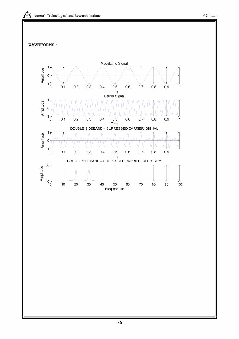
3 DOUBLE SIDEBAND ndash SUPRESSED CARRIER MODULATION
AND DEMODULATION
PROGRAM 1 clc clear all close all Ts = 199 subplot(411) t = 01Ts1 m = cos(2pi1000t) plot(tm) title(Modulating Signal ) xlabel(Time) ylabel(Amplitude) grid on plot of the carrier signal
subplot(412) c = cos(2pi5000t) plot(tc) title(Carrier Signal ) xlabel(Time) ylabel(Amplitude) grid on plot of the DSB signal with Suppresed carrier intime domain
subplot(413) d = mc plot(td) title(DOUBLE SIDEBAND ndash SUPRESSED CARRIER SIGNAL ) xlabel(Time) ylabel(Amplitude) grid on freq domain of the DSB signal
subplot(414) fre = abs(fft(d)) f = (0length(fre) - 1)Tslength(fre) plot(ffre) axis([0 100 0 50]) grid on title(DOUBLE SIDEBAND ndash SUPRESSED CARRIER SPECTRUM ) xlabel(Freq domain) ylabel(Amplitude)
Aurorarsquos Technological and Research Institute AC Lab
86
WAVEFORMS
0 01 02 03 04 05 06 07 08 09 1-1
0
1Modulating Signal
Time
Am
plit
ude
0 01 02 03 04 05 06 07 08 09 1-1
0
1Carrier Signal
Time
Am
plit
ude
0 01 02 03 04 05 06 07 08 09 1-1
0
1DOUBLE SIDEBAND ndash SUPRESSED CARRIER SIGNAL
Time
Am
plit
ude
0 10 20 30 40 50 60 70 80 90 1000
50DOUBLE SIDEBAND ndash SUPRESSED CARRIER SPECTRUM
Freq domain
Am
plit
ude
Aurorarsquos Technological and Research Institute AC Lab
87
PROGRAM 2 task 1 fc=154000 task 2 fm=fc10 fs=100fc t=01fs4fm xc=cos(2pifct) xm=cos(2pifmt) figure(1) subplot(211)plot(txc) title(carrier signal of 154 khz) xlabel(time (sec)) ylabel(amplitude) subplot(212)plot(txm) title(message signal of 154 khz) xlabel(time (sec)) ylabel(amplitude) DSB-SC MODULATION z1= xmxc figure(2) task 31 subplot(211)plot(tz1) title(DSB-SC MODULATION IN TIME DAOMAIN) xlabel(time (sec)) ylabel(amplitude) task 32 l1=length(z1) f=linspace(-fs2fs2l1) Z1=fftshift(fft(z1l1)l1) subplot(212)plot(fabs(Z1)) title(DSB SC MODULATION IN FREQUENCY DOMAIN) xlabel(frequency(hz)) ylabel(amplitude) axis([-200000 200000 0 03]) task 33 demodulation s1=z1xc S1=fftshift(fft(s1length(s1))length(s1)) figure(3) plot(fabs(S1)) title( demodulated signal IN FREQUENCY DOMAIN before filtring) xlabel(frequency(hz)) ylabel(amplitude) axis([-200000 200000 0 03]) hold on Hlp=1sqrt(1+(ffc)^(2100)) plot(fHlpg) title( frequency response of low pass filter) xlabel(frequency(hz)) ylabel(amplitude) axis([-200000 200000 0 2]) task 34 E1=HlpS1 figure(4) subplot(211)plot(fE1) title( Recover signal IN FREQUENCY DOMAIN after filtring) xlabel(frequency(hz)) ylabel(amplitude) axis([-200000 200000 0 03]) e1=ifft(ifftshift(E1))length(E1) subplot(212)plot(t(105)e1)
Aurorarsquos Technological and Research Institute AC Lab
88
title( Recover signal IN Time DOMAIN after filtring) xlabel(time(sec)) ylabel(amplitude) WAVEFORMS
0 1 2 3
x 10-4
-1
-05
0
05
1carrier signal of 154 khz
time (sec)
ampl
itude
0 1 2 3
x 10-4
-1
-05
0
05
1message signal of 154 khz
time (sec)
ampl
itude
0 1 2 3
x 10-4
-1
-05
0
05
1DSB-SC MODULATION IN TIME DAOMAIN
time (sec)
ampl
itude
-2 -15 -1 -05 0 05 1 15 2
x 105
0
01
02
DSB SC MODULATION IN FREQUENCY DOMAIN
frequency(hz)
ampl
itude
Aurorarsquos Technological and Research Institute AC Lab
89
-2 -15 -1 -05 0 05 1 15 2
x 105
0
02
04
06
08
1
12
14
16
18
2 frequency response of low pass filter
frequency(hz)
ampl
itude
-2 -15 -1 -05 0 05 1 15 2
x 105
0
01
02
Recover signal IN FREQUENCY DOMAIN after filtring
frequency(hz)
am
plit
ude
0 1 2 3
x 10-4
-1
0
1
2 Recover signal IN Time DOMAIN after filtring
time(sec)
am
plit
ude
Aurorarsquos Technological and Research Institute AC Lab
90
4 SINGLE SIDE BAND - SUPRESSED CARRIER MODULATION AND DEMODULATION
PROGRAM 1
clc clear all close all Ts = 199 subplot(411) t = 01Ts1 xm = cos(2pi1000t) plot(txm) title(Modulating Signal ) xlabel(Time) ylabel(Amplitude) grid on plot of the carrier signal subplot(412) c = cos(2pi5000t) plot(tc) title(Carrier Signal ) xlabel(Time) ylabel(Amplitude) grid on subplot(413) helbert transform of messeage signal xh=cos((2pi1000t)-pi2) SSB UPPER SIDE BAND MODULATION d= (xmcos(2pi5000t))-(xhsin(2pi5000t)) plot(td) title(SINGLE SIDEBAND ndash SUPRESSED CARRIER SIGNAL ) xlabel(Time) ylabel(Amplitude) grid on freq domain of the DSB signal subplot(414) fre = abs(fft(d)) f = (0length(fre) - 1)Tslength(fre) plot(ffre) axis([0 100 0 50]) grid on title(SINGLE SIDEBAND ndash SUPRESSED CARRIER SPECTRUM ) xlabel(Freq domain) ylabel(Amplitude)
Aurorarsquos Technological and Research Institute AC Lab
91
WAVEFORMS
0 01 02 03 04 05 06 07 08 09 1-1
0
1Modulating Signal
Time
Am
plit
ude
0 01 02 03 04 05 06 07 08 09 1-1
0
1Carrier Signal
Time
Am
plit
ude
0 01 02 03 04 05 06 07 08 09 1-1
0
1SINGLE SIDEBAND ndash SUPRESSED CARRIER SIGNAL
Time
Am
plit
ude
0 10 20 30 40 50 60 70 80 90 1000
50SINGLE SIDEBAND ndash SUPRESSED CARRIER SPECTRUM
Freq domain
Am
plit
ude
Aurorarsquos Technological and Research Institute AC Lab
92
PROGRAM 2
task 1 fc=154000
task 2 fm=fc10 fs=100fc t=01fs4fm xc=cos(2pifct) xm=cos(2pifmt)
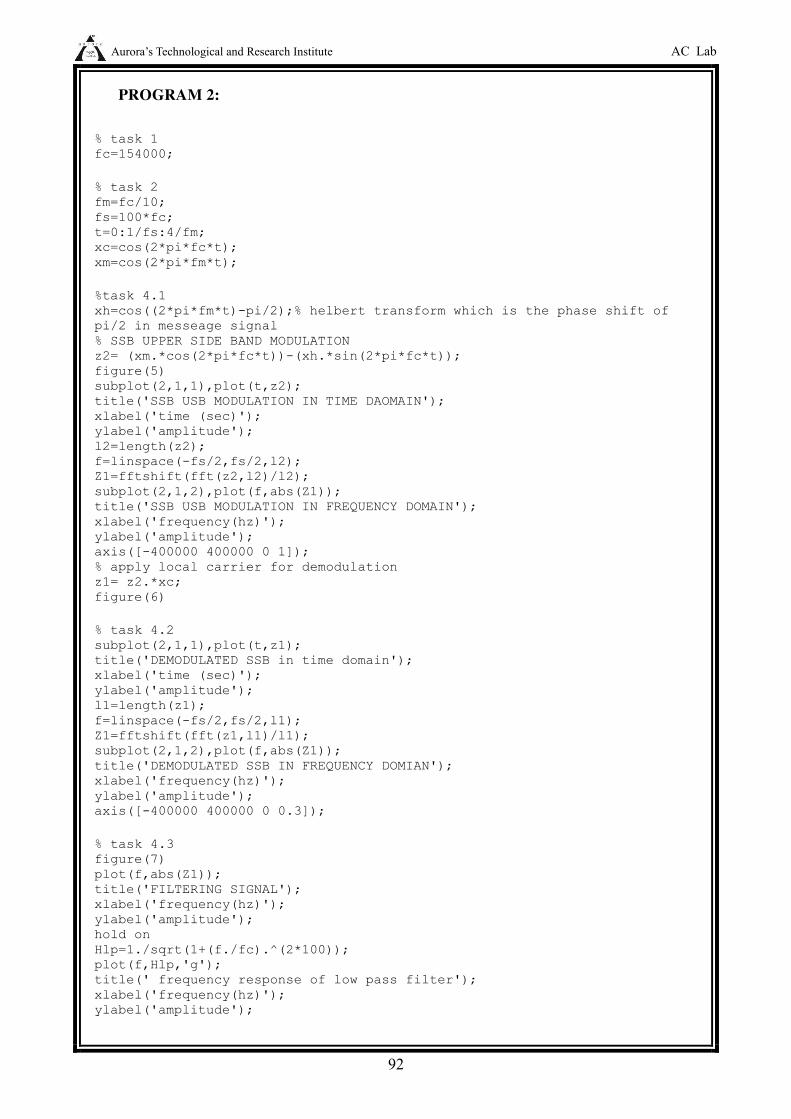
task 41 xh=cos((2pifmt)-pi2) helbert transform which is the phase shift of pi2 in messeage signal SSB UPPER SIDE BAND MODULATION z2= (xmcos(2pifct))-(xhsin(2pifct)) figure(5) subplot(211)plot(tz2) title(SSB USB MODULATION IN TIME DAOMAIN) xlabel(time (sec)) ylabel(amplitude) l2=length(z2) f=linspace(-fs2fs2l2) Z1=fftshift(fft(z2l2)l2) subplot(212)plot(fabs(Z1)) title(SSB USB MODULATION IN FREQUENCY DOMAIN) xlabel(frequency(hz)) ylabel(amplitude) axis([-400000 400000 0 1]) apply local carrier for demodulation z1= z2xc figure(6)
task 42 subplot(211)plot(tz1) title(DEMODULATED SSB in time domain) xlabel(time (sec)) ylabel(amplitude) l1=length(z1) f=linspace(-fs2fs2l1) Z1=fftshift(fft(z1l1)l1) subplot(212)plot(fabs(Z1)) title(DEMODULATED SSB IN FREQUENCY DOMIAN) xlabel(frequency(hz)) ylabel(amplitude) axis([-400000 400000 0 03])
task 43 figure(7) plot(fabs(Z1)) title(FILTERING SIGNAL) xlabel(frequency(hz)) ylabel(amplitude) hold on Hlp=1sqrt(1+(ffc)^(2100)) plot(fHlpg) title( frequency response of low pass filter) xlabel(frequency(hz)) ylabel(amplitude)
Aurorarsquos Technological and Research Institute AC Lab
93
axis([-400000 400000 0 2])
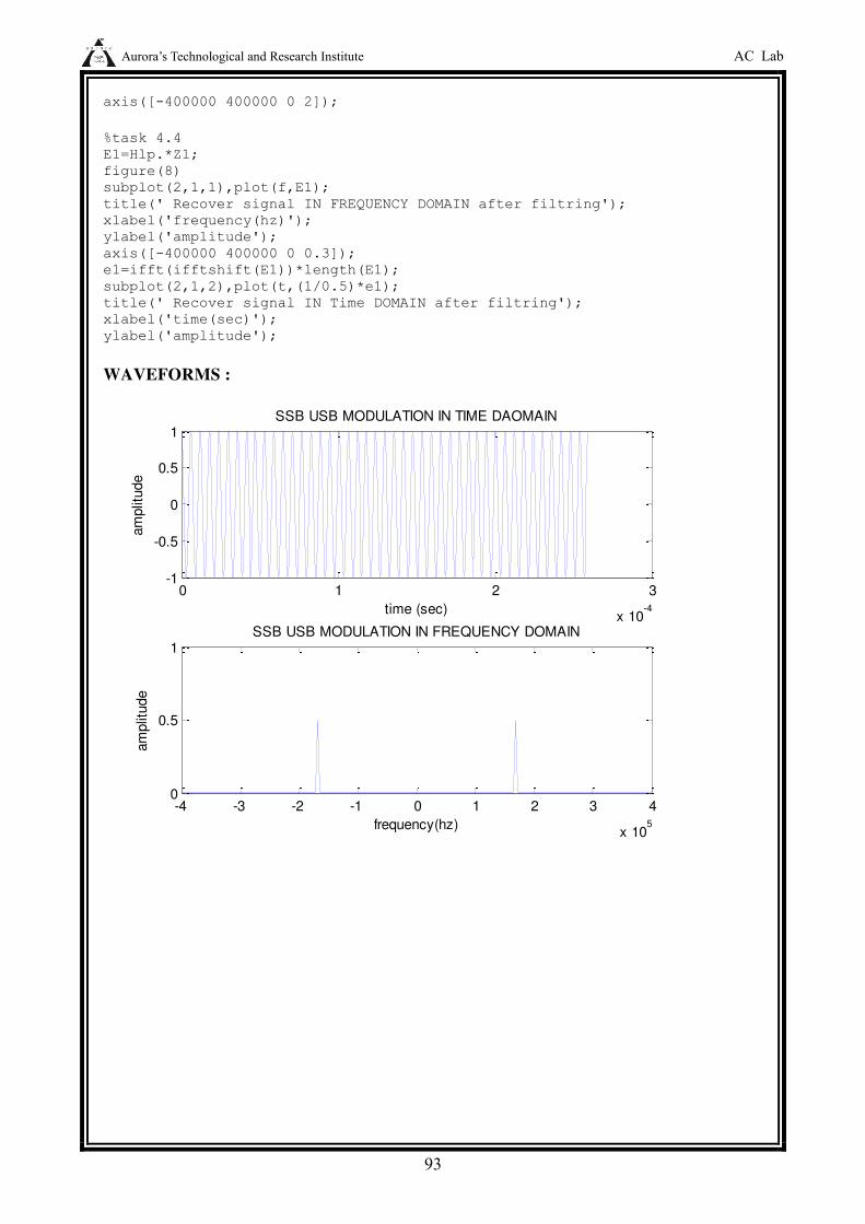
task 44 E1=HlpZ1 figure(8) subplot(211)plot(fE1) title( Recover signal IN FREQUENCY DOMAIN after filtring) xlabel(frequency(hz)) ylabel(amplitude) axis([-400000 400000 0 03]) e1=ifft(ifftshift(E1))length(E1) subplot(212)plot(t(105)e1) title( Recover signal IN Time DOMAIN after filtring) xlabel(time(sec)) ylabel(amplitude)
WAVEFORMS
0 1 2 3
x 10-4
-1
-05
0
05
1SSB USB MODULATION IN TIME DAOMAIN
time (sec)
am
plit
ude
-4 -3 -2 -1 0 1 2 3 4
x 105
0
05
1SSB USB MODULATION IN FREQUENCY DOMAIN
frequency(hz)
am
plit
ude
Aurorarsquos Technological and Research Institute AC Lab
94
0 1 2 3
x 10-4
-1
-05
0
05
1DEMODULATED SSB in time domain
time (sec)
am
plit
ude
-4 -3 -2 -1 0 1 2 3 4
x 105
0
01
02
DEMODULATED SSB IN FREQUENCY DOMIAN
frequency(hz)
am
plit
ude
-4 -3 -2 -1 0 1 2 3 4
x 105
0
02
04
06
08
1
12
14
16
18
2 frequency response of low pass filter
frequency(hz)
am
plit
ude
Aurorarsquos Technological and Research Institute AC Lab
95
-4 -3 -2 -1 0 1 2 3 4
x 105
0
01
02
Recover signal IN FREQUENCY DOMAIN after filtring
frequency(hz)
am
plit
ude
0 1 2 3
x 10-4
-1
0
1
2 Recover signal IN Time DOMAIN after filtring
time(sec)
am
plit
ude
Aurorarsquos Technological and Research Institute AC Lab
96
5 FREQUENCY MODULATION AND DEMODULATION
clc clear all close all Frequency MODULATION of Triangular Signal t = -0041e-4004 Ta = 001 fc = 200 Frequency of carrier msg = msg1(tTa) Calling Function to Generate Msg Signal MODULATION kf = 160pi m_int = kf1e-4cumsum(msg) Integrating Msg fm = cos(2fcpit + m_int) fm = cos(2pifct + integral(msg)) DEMODULATION (Using Differentiator) dem = diff(fm) dem = [0dem] rect_dem = abs(dem) Filtering out High Frequencies N = 80 Order of Filter Wn = 1e-2 Pass Band Edge Frequency a = fir1(NWn) Return Numerator of Low Pass FIR filter b = 1 Denominator of Low Pass FIR Filter rec = filter(abrect_dem) Finding frequency Response of Signals fl = length(t) fl = 2^ceil(log2(fl)) f = (-fl2fl2-1)(fl1e-4) mF = fftshift(fft(msgfl)) Frequency Response of Message Signal fmF = fftshift(fft(fmfl)) Frequency Response of FM Signal Frequency Response of Rectified FM Signal rect_demF = fftshift(fft(rect_demfl)) Frequency Response of Recovered Message Signal recF = fftshift(fft(recfl)) Plotting signal in time domain figure subplot(211) plot(tmsg) title(Message Signal) xlabel(it t (sec)) ylabel(Amplitude)) grid subplot(212) plot(tfm)
Aurorarsquos Technological and Research Institute AC Lab
97
title(FM) xlabel(it t (sec)) ylabel(Amplitude) grid figure subplot(211) plot(trect_dem) title(Rectified FM) xlabel(it t (sec)) ylabel(Amplitude) grid subplot(212) plot(trec) title(Recovered Signal) xlabel(it t (sec)) ylabel(Amplitude) grid Plotting Freq Response of Signals figure subplot(221) plot(fabs(mF)) title(Freq Response of MSG) xlabel(f(Hz)) ylabel(Amplitude) grid axis([-600 600 0 200]) subplot(222) plot(fabs(fmF)) title(Freq Response of FM) grid xlabel(f(Hz)) ylabel(Amplitude) axis([-600 600 0 300]) subplot(223) plot(fabs(rect_demF)) title(Freq Response of Rectified FM) xlabel(f(Hz)) ylabel(Amplitude) grid axis([-600 600 0 100]) subplot(224) plot(fabs(recF)) title(Freq Response of Recovered Signal) xlabel(f(Hz)) ylabel(Amplitude) grid axis([-600 600 0 100])
Function to give message signal
Function of Msg(tri) function a = msg1(tTa) t1 = -0021e-40
Aurorarsquos Technological and Research Institute AC Lab
98
t2 = 01e-4002 m1 = 1 - abs((t1+Ta)Ta) m1 = [zeros([1 200])m1zeros([1 400])] m2 = 1 - abs((t2-Ta)Ta) m2 = [zeros([1 400])m2zeros([1 200])] a = m1 - m2 end
WAVEFORMS
-004 -003 -002 -001 0 001 002 003 004-1
-05
0
05
1Message Signal
t (sec)
Am
plit
ude)
-004 -003 -002 -001 0 001 002 003 004-1
-05
0
05
1FM
t (sec)
Am
plit
ude
Aurorarsquos Technological and Research Institute AC Lab
99
-004 -003 -002 -001 0 001 002 003 0040
005
01
015
02Rectified FM
t (sec)
Am
plit
ude
-004 -003 -002 -001 0 001 002 003 0040
005
01
015
02Recovered Signal
t (sec)
Am
plit
ude
-500 0 5000
50
100
150
200Freq Response of MSG
f(Hz)
Am
plit
ude
-500 0 5000
100
200
300Freq Response of FM
f(Hz)
Am
plit
ude
-500 0 5000
50
100Freq Response of Rectified FM
f(Hz)
Am
plit
ude
-500 0 5000
50
100Freq Response of Recovered Signal
f(Hz)
Am
plit
ude
Aurorarsquos Technological and Research Institute AC Lab
100
6 PHASE MODULATION AND DEMODULATION
clear all close all t = 00011 time variable fc = 5 carrier frequency ------------------------------------------ create message signal m(t) m = sin(2pit) ------------------------------------------ kp = pi2 phase deviation constant ------------------------------------------------ modulating the carrier with the message signal carrier = cos(2pifct) modulated = cos(2pifct + kpm) ------------------------------------------------ ------------------------------------------------ Plotting the signals plot(tmbtcarrierrtmodulatedk--) axis([0 1 -15 15]) xlabel(Time(seconds)) ylabel(Amplitude(volt)) title(Phase modulation) legend(MessageCarrierModulated)
WAVEFORMS
0 01 02 03 04 05 06 07 08 09 1-15
-1
-05
0
05
1
15
Time(seconds)
Am
plit
ude(v
olt)
Phase modulation
Message
Carrier
Modulated
Aurorarsquos Technological and Research Institute AC Lab
101
7 TIME DIVISION MULTIPLEXING AND DEMULTIPLEXING clc close all clear all Signal generation x=058pi sig1=8sin(x-pi) generate 1st sinusoidal signal l=length(sig1) sig2=8square(x) Generate 2nd traingular Sigal Display of Both Signal subplot(221) plot(sig1) title(Sinusoidal Signal) ylabel(Amplitude---gt) xlabel(Time---gt) subplot(222) plot(sig2) title(Triangular Signal) ylabel(Amplitude---gt) xlabel(Time---gt) Display of Both Sampled Signal subplot(223) stem(sig1) title(Sampled Sinusoidal Signal) ylabel(Amplitude---gt) xlabel(Time---gt) subplot(224) stem(sig2) title(Sampled Triangular Signal) ylabel(Amplitude---gt) xlabel(Time---gt) l1=length(sig1) l2=length(sig2) for i=1l1 sig(1i)=sig1(i) sig(2i)=sig2(i) end TDM of both quantize signal tdmsig=reshape(sig12l1) Display of TDM Signal figure stem(tdmsig) title(TDM Signal) ylabel(Amplitude---gt) xlabel(Time---gt) Demultiplexing of TDM Signal demux=reshape(tdmsig2l1) for i=1l1 sig3(i)=demux(1i) sig4(i)=demux(2i) end
display of demultiplexed signal figure subplot(211)
Aurorarsquos Technological and Research Institute AC Lab
102
plot(sig3) title(Recovered Sinusoidal Signal) ylabel(Amplitude---gt) xlabel(Time---gt) subplot(212) plot(sig4) title(Recovered Triangular Signal) ylabel(Amplitude---gt) xlabel(Time---gt)
WAVEFORMS
0 20 40 60-10
-5
0
5
10Sinusoidal Signal
Am
plit
ude--
-gt
Time---gt
0 20 40 60-10
-5
0
5
10Square Signal
Am
plit
ude--
-gt
Time---gt
0 20 40 60-10
-5
0
5
10Sampled Sinusoidal Signal
Am
plit
ude--
-gt
Time---gt
0 20 40 60-10
-5
0
5
10Sampled Square Signal
Am
plit
ude--
-gt
Time---gt
Aurorarsquos Technological and Research Institute AC Lab
103
0 20 40 60 80 100 120-8
-6
-4
-2
0
2
4
6
8TDM Signal
Am
plit
ude--
-gt
Time---gt
0 10 20 30 40 50 60-10
-5
0
5
10Recovered Sinusoidal Signal
Am
plit
ude--
-gt
Time---gt
0 10 20 30 40 50 60-10
-5
0
5
10Recovered Square Signal
Am
plit
ude--
-gt
Time---gt
Aurorarsquos Technological and Research Institute AC Lab
104
8 FREQUENCY DIVISION MULTIPLEXING AND
DEMULTIPLEXING
Aurorarsquos Technological and Research Institute AC Lab
105
9 VERIFICATION OF SAMPLING THEOREM [
clear all close all clc Fs = input(Enter Sampling Frequency in Hz ) Fm = input(Enter Message Frequency in Hz ) t = 00012 msg = sin(2pit) k = 2FsFm step = ceil(201k) samp_msg = [] for i = 1201 if (mod(istep) == 0) samp_msg = [samp_msgmsg(i)] else samp_msg = [samp_msgzeros(1)] end end subplot(211) plot(msg) xlabel(---gt Time) ylabel(---gt Amplitude) title(Msg signal) subplot(212) stem(samp_msg) xlabel(---gt Time) ylabel(---gt Amplitude) if Fs lt 2Fm title(Under Sampling) else if Fs == 2Fm title(Critical Sampling) else title(Over Sampling) end end
WAVEFORMS
Enter Sampling Frequency in Hz 1200
Enter Message Frequency in Hz 60
Aurorarsquos Technological and Research Institute AC Lab
106
Enter Sampling Frequency in Hz 100
Enter Message Frequency in Hz 60
0 50 100 150 200 250-1
-05
0
05
1
---gt Time
---gt
Am
plit
ude
Msg signal
0 50 100 150 200 250-1
-05
0
05
1
---gt Time
---gt
Am
plit
ude
Over Sampling
0 50 100 150 200 250-1
-05
0
05
1
---gt Time
---gt
Am
plit
ude
Msg signal
0 50 100 150 200 250-1
-05
0
05
1
---gt Time
---gt
Am
plit
ude
Under Sampling
Aurorarsquos Technological and Research Institute AC Lab
107
10 PULSE AMPLITUDE MODULATION AND
DEMODULATION
clear all close all clc t = 000100013 msg = sin(2pit) subplot(311) plot(msg) title(Message Signal ) xlabel(Time) ylabel(Amplitude) x = [ones(150)zeros(1100)] car = [] for i = 120 car = [carx] end subplot(312) plot(car) title(Carrier Signal ) xlabel(Time) ylabel(Amplitude) mm = msgcar tt = [] for i =13000 if mm(i) == 0 tt = [ttmm(i)] else tt = [ttmm(i)+2] end end subplot(313) stem(ttr) title(PAM signal ) xlabel(Time) ylabel(Amplitude)
WAVEFORMS
Aurorarsquos Technological and Research Institute AC Lab
108
0 500 1000 1500 2000 2500 3000-1
0
1Message Signal
Time
Am
plit
ude
0 500 1000 1500 2000 2500 30000
05
1Carrier Signal
Time
Am
plit
ude
0 500 1000 1500 2000 2500 30000
2
4PAM signal
Time
Am
plit
ude
Aurorarsquos Technological and Research Institute AC Lab
109
11 PULSE WIDTH MODULATION AND DEMODULATION
fc = 1000 fs = 10000 f1 = 200 f2 = 300 t = 01fs((2f1)-(1fs)) x1 = 04cos(2pif1t)+05 x2 = 02(cos(2pif1t)+cos(2pif2t))+05 MODULATION y1 = modulate(x1fcfspwm) subplot(211) plot(x1) title(Original single tone message f1 = 200 fs = 10000) subplot(212) plot(y1) title(PWM on cycle of f1 = 200 fc = 1000) axis([0500-0212]) figure fx1 = abs(fft(y11024)) fx1 = [fx1(5141024) fx1(1513)] f = (-511fs1024)(fs1024)(512fs1024) subplot(211) plot(ffx1) title(Frequency description single tone f1 = 200 fc = 1000) DEMODULATION x1_recov = demod(y1fcfspwm) subplot(212) plot(x1_recov ) title(Time domain recovered single tone f1 = 200 )
WAVEFORMS
Aurorarsquos Technological and Research Institute AC Lab
110
0 10 20 30 40 50 60 70 80 90 1000
05
1Original single tone message f1 = 200 fs = 10000
0 50 100 150 200 250 300 350 400 450 500
0
05
1
PWM on cycle of f1 = 200 fc = 1000
-5000 -4000 -3000 -2000 -1000 0 1000 2000 3000 4000 50000
200
400
600Frequency description single tone f1 = 200 fc = 1000
0 10 20 30 40 50 60 70 80 90 1000
05
1Time domain recovered single tone f1 = 200
Aurorarsquos Technological and Research Institute AC Lab
111
12 PULSE POSITION MODULATION AND DEMODULATION fc = 1000 fs = 10000 f1 = 200 f2 = 300 t = 01fs((2f1)-(1fs)) x1 = 04cos(2pif1t)+05 x2 = 02(cos(2pif1t)+cos(2pif2t))+05 MODULATION y1 = modulate(x1fcfsppm) subplot(211) plot(x1) title(Original single tone message f1 = 200 fs = 10000) subplot(212) plot(y1) title(PPM on cycle of f1 = 200 fc = 1000) axis([0500-0212]) figure fx1 = abs(fft(y11024)) fx1 = [fx1(5141024) fx1(1513)] f = (-511fs1024)(fs1024)(512fs1024) subplot(211) plot(ffx1) title(Frequency description single tone f1 = 200 fc = 1000) DEMODULATION x1_recov = demod(y1fcfsppm) subplot(212) plot(x1_recov ) title(Time domain recovered single tone f1 = 200 )
WAVEFORMS
Aurorarsquos Technological and Research Institute AC Lab
112
0 10 20 30 40 50 60 70 80 90 1000
05
1Original single tone message f1 = 200 fs = 10000
0 50 100 150 200 250 300 350 400 450 500
0
05
1
PPM on cycle of f1 = 200 fc = 1000
-5000 -4000 -3000 -2000 -1000 0 1000 2000 3000 4000 50000
50
100Frequency description single tone f1 = 200 fc = 1000
0 10 20 30 40 50 60 70 80 90 1000
05
1Time domain recovered single tone f1 = 200
Aurorarsquos Technological and Research Institute AC Lab
113
13 PHASE LOCKED LOOP AS FM DEMODULATOR
This m-file demonstrates a PLL which tracks and demodulates an FM carrier clear all close all f=1000 Carrier frequency fs=100000 Sample frequency N=5000 Number of samples Ts=1fs t=(0Ts(NTs)- Ts)
Create the message signal f1=100 Modulating frequency msg=sin(2pif1t) kf=0628 Modulation index
Create the real and imaginary parts of a CW modulated carrier to be tracked
Signal=exp(j(2pift+2pikfcumsum(msg))) Modulated carrier Signal1=exp(j(2pift)) Unmodulated carrier
Initilize PLL Loop phi_hat(1)=30 e(1)=0 phd_output(1)=0 vco(1)=0
Define Loop Filter parameters(Sets damping) kp=015 Proportional constant ki=01 Integrator constant
PLL implementation for n=2length(Signal) vco(n)=conj(exp(j(2pinffs+phi_hat(n-1)))) Compute VCO phd_output(n)=imag(Signal(n)vco(n)) Complex multiply VCO x Signal
input Filter integrator
e(n)=e(n-1)+(kp+ki)phd_output(n)-kiphd_output(n-1) phi_hat(n)=phi_hat(n-1)+e(n)Update VCO end
Plot waveforms startplot = 1 endplot = 1000 figure(1) subplot(321) plot(t(startplotendplot) msg(startplotendplot)) title(100 Hz message signal) ylabel(Amplitude) grid figure(1) subplot(322) plot(t(startplotendplot) real(Signal(startplotendplot))) title(FM (1KHz carrier modulated with a 100 Hz message signal)) ylabel(Amplitude) grid figure(1) subplot(323) plot(t(startplotendplot) e(startplotendplot)) title(PLL Loop FilterIntegrator Output)
Aurorarsquos Technological and Research Institute AC Lab
114
ylabel(Amplitude) grid subplot(324) plot(t(startplotendplot) real(vco(startplotendplot))) title(VCO Output (PLL tracking the input signal)) ylabel(Amplitude) grid subplot(325) plot(t(startplotendplot) phd_output(startplotendplot)) title(Phase Detecter Output) xlabel(Time (seconds)) ylabel(Amplitude) grid subplot(326) plot(t(startplotendplot) real(Signal1(startplotendplot))) title(Unmodulated Carrier) xlabel(Time (seconds)) ylabel(Amplitude) grid
WAVEFORMS
0 0002 0004 0006 0008 001-1
0
1100 Hz message signal
Am
plit
ude
0 0002 0004 0006 0008 001-1
0
1FM (1KHz carrier modulated with a 100 Hz message signal)
Am
plit
ude
0 0002 0004 0006 0008 001-05
0
05PLL Loop FilterIntegrator Output
Am
plit
ude
0 0002 0004 0006 0008 001-1
0
1VCO Output (PLL tracking the input signal)
Am
plit
ude
0 0002 0004 0006 0008 001-1
0
1Phase Detecter Output
Time (seconds)
Am
plit
ude
0 0002 0004 0006 0008 001-1
0
1Unmodulated Carrier
Time (seconds)
Am
plit
ude
- Electronic phase detector
-

Auroras Technological and Research Institute AC Lab
Department of ECE 6
GENERAL LABORATORY INSTRUCTIONS
You should be punctual for your laboratory session and should not leave the lab without the
permission of the teacher
Each student is expected to have hisher own lab book where they will take notes on the experiments
as they are completed The lab books will be checked at the end of each lab session Lab notes are a
primary source from which you will write your lab reports
Organization of the Laboratory
It is important that the programs are done according to the timetable and completed within the
scheduled time
You should complete the prelab work in advance and utilize the laboratory time for verification only
The aim of these exercises is to develop your ability to understand analyze and test them in the
laboratory
A member of staff and a Lab assistant will be available during scheduled laboratory sessions to
provide assistance
Always attempt program first without seeking help
When you get into difficulty ask for assistance
Assessment
The laboratory work of a student will be evaluated continuously during the semester for 25 marks Of
the 25 marks 15 marks will be awarded for day-to-day work For each program marks are awarded
under three heads
Prelab preparation ndash 5 marks
Practical work ndash 5marks and
Record of the Experiment ndash 5marks
Internal lab test(s) conducted during the semester carries 10 marks
End semester lab examination conducted as per the JNTU regulations carries 50 marks
At the end of each laboratory session you must obtain the signature of the teacher along with the
marks for the session out of 10 on the lab notebook
Lab Reports
Note that although students are encouraged to collaborate during lab each must individually prepare a
report and submit
They must be organized neat and legible
Your report should be complete thorough understandable and literate
You should include a well-drawn and labeled engineering schematic for each circuit investigated
Your reports should follow the prescribed format to give your report structure and to make sure that
you address all of the important points
Graphics requiring- drawn straight lines should be done with a straight edge Well drawn free-hand
sketches are permissible for schematics
Auroras Technological and Research Institute AC Lab
Department of ECE 7
Space must be provided in the flow of your discussion for any tables or figures Do not collect figures
and drawings in a single appendix at the end of the report
Reports should be submitted within one week after completing a scheduled lab session
Presentation
Experimental facts should always be given in the past tense
Discussions or remarks about the presentation of data should mainly be in the present tense
Discussion of results can be in both the present and past tenses shifting back and forth from
experimental facts to the presentation
Any specific conclusions or deductions should be expressed in the past tense
Report Format
Lab write ups should consist of the following sections
Aim
Equipments
Circuit Diagram
Theory
Procedure
Expected Waveform
Observation and Calculations
Results
Conclusions
Note Diagrams if any must be drawn neatly on left hand side
Auroras Technological and Research Institute AC Lab
Department of ECE 8
LIST OF EXPERIMENTS
1 Amplitude Modulation and Demodulation
2 DSB ndash SC Modulator amp Detector
3 SSB-SC Modulator amp Detector (Phase Shift Method)
4 Frequency Modulation and Demodulation
5 Study of Spectrum analyzer and Analysis of AM and FM Signals
6 Pre-emphasis amp De-emphasis
7 Time Division Multiplexing amp De multiplexing
8 Frequency Division Multiplexing amp De multiplexing
9 Verification of Sampling Theorem
10 Pulse Amplitude Modulation amp Demodulation
11 Pulse Width Modulation amp Demodulation
12 Pulse Position Modulation amp Demodulation
13 Frequency Synthesizer
14 AGC Characteristics
15 PLL as FM Demodulator
Annexure I Additional Experiments
1 Characteristics of Mixer
2 Digital Phase Detector
3 Coastas Receiver
Auroras Technological and Research Institute AC Lab
Department of ECE 9
EXPERIMENT NO 1
AMPLITUDE MODULATION amp DEMODULATION OBJECTIVE
To study
1 Amplitude modulation process
2 Measurement of Modulation Index
3 Effect of 100 Modulation over modulation under modulation
4 Demodulation Process
PRE-LAB
1 Study the theory of Amplitude Modulation and Demodulation
2 Draw the circuit diagram for Modulation and Demodulation
3 Draw the expected wave forms for different values of modulation index
COMPONENTS
1 Amplitude Modulation and Demodulation Trainer Kit 1 No 2 CRO Dual Trace 1 No 3 Connecting Probe and Cords
BRIEF THEORY
If you connect a long wire to the output terminals of your Hi-Fi amplifier and another long wire to the input of another amplifier you can transmit music over a short distance DONT try this You could blow up your amplifier
A radio wave can be transmitted long distances To get our audio signal to travel long distances we piggyback it onto a radio wave This process is called MODULATION
The radio wave is called the CARRIER The audio signal is called the MODULATION At the receiving end the audio is recovered by a process called DEMODULATION From the diagram below it can be seen that when the carrier is modulated its amplitude goes above and below its unmodulated amplitude It is about 50 modulated in the
Auroras Technological and Research Institute AC Lab
Department of ECE 10
diagram The maximum percentage modulation possible is 100 Going above this causes distortion
Most broadcasters limit modulation to 80Modulating the carrier frequency with an audio frequency produces two new frequencies At this point it would be a good idea to read the page on MIXERS These new frequencies are called the upper and lower SIDEBANDS The upper sideband is the carrier frequency plus the audio frequency The lower side band is the carrier frequency minus the audio frequencySince the audio signal is not a single frequency but a range of signals (usually 20 Hz to 20 KHz) the sidebands are each 20Hz to 20 KHz wide
If you tune across a station in the Medium Wave Band you will find that it takes up space in the band This is called the signal BANDWIDTH This is the space taken by the upper and lower sidebands In the the example given above it would be 40 KHz Since the Medium Wave is only 500 KHZ wide there would only be space for about 12 stations Therefore the bandwidth of stations is limited to 9 KHz which limits the audio quality If there are two stations too close together their sidebands mix and produce HETERODYNE whistles Since both sidebands carry
Auroras Technological and Research Institute AC Lab
Department of ECE 11
CIRCUIT DIAGRAMS
AM MODULATION
AM DEMODULATION
CARRIER SIGNAL
TIME T
A
m
p
l i t u
d
e
Ac
Auroras Technological and Research Institute AC Lab
Department of ECE 12
MODULATING SIGNAL
AM MODULATED OUTPUT
AM DEMODULATION OUTPUT
PROCEDURE
A MODULATION i Switch lsquoONrsquo the Trainer Kit
ii Generate the carrier and modulating signal such that carrier frequency must be greater than modulating frequency
iii Apply the carrier and modulating signal into AM modulator input vi Trace the envelope of the modulated waveform
v Repeat step(vi) duly adjusting the modulating signal for under modulation and over modulation
B DEMODULATION
i Apply the modulated AM output into Demodulation input ii Trace the demodulated output waveform
POST- LAB
TIME T
A
m
p
l i t u
d
e
Am
A
m
p
l i t u
d
e
TIME T
Auroras Technological and Research Institute AC Lab
Department of ECE 13
i Observe the frequency and amplitude of the carrier and modulating signal
ii Observe the frequency and maximum peak-peak amplitude(Amax) and minimum peak-
peak amplitude (Amin) of the AM signal in TableI
iii Calculate the modulation index Ч=Amax-AminAmax+Amin
iv Plot the out put waveforms Time T Vs Voltage Vo
v Write result and conclusion
CONCLUSION Hence the AM modulation and demodulation is verified
QUESTIONS 1 what is meant by modulation
2 What is meant by modulation index
3 What is meant by under modulation and over modulation
Auroras Technological and Research Institute AC Lab
Department of ECE 14
EXPERIMENT NO 2
DSB ndash SC Modulator amp Demodulator
OBJECTIVE To study the balanced modulator using IC 1496
PRE-LAB
1 Study the theory of balanced modulator
2 Draw the circuit diagram
3 Draw the expected waveforms
4 Study the datasheet of IC 1496
EQUIPMENT
1 Function generator
2 Dual trace CRO
3 Balanced modulator trainer kit
THEORY
In a balanced modulator a signal is modulated using two carriers that are 180
degrees out of phase The resulting signals are then combined in such a way that the carrier
components cancel leaving a DSB-SC (double sideband suppressed carrier) signal
CIRCUIT DIAGRAM
Auroras Technological and Research Institute AC Lab
Department of ECE 15
BALANCED MODULATOR OUTPUT
Auroras Technological and Research Institute AC Lab
Department of ECE 16
BALANCED DEMODULATOR OUTPUT
PROCEDURE
1 Switch ON the trainer kit
2 Generate the carrier and modulating signal
3 Apply the modulating signal and the carrier signal to the balanced modulator input
4 Observe the balanced modulator output
POST LAB
1 Observe the frequency and amplitude of the carrier and modulating signal
2 Observe the frequency and amplitude of the balanced modulator output
3 Observe the quadrature null effect
4 Plot the output waveforms Time T VS Voltage V
5 Write result and conclusions
CONCLUSIONS The balanced modulator output is verified
QUESTIONS 1 what is the efficiency for DSB SC signal
2 What are the other types of balanced modulators
3 What is meant by pilot carrier
Auroras Technological and Research Institute AC Lab
Department of ECE 17
EXPERIMENT NO 3
SSB ndash SC MODULATOR amp DEMODULATOR
OBJECTIVE To study the Single side band modulation by using Phase shift method and demodulation using synchronous detector method
PRE-LAB
1 Study the theory of SSB
2 Draw the circuit diagram and expected waveforms
EQUIPMENTS 1 Function generator 2
2 Dual trace CRO 1
3 SSB system modulation and demodulation trainer kit 4 Patch CardsConnecting wires
5 Frequency counterMulti meter
THEORY
Single-sideband modulation (SSB) is a refinement of amplitude modulation that more
efficiently uses electrical power and bandwidth It is closely related to vestigial sideband
modulation (VSB)Amplitude modulation produces a modulated output signal that has
twice the bandwidth of the original baseband signal Single-sideband modulation avoids
this bandwidth doubling and the power wasted on a carrier at the cost of somewhat
increased device complexity SSB was also used over long distance telephone lines as part
of a technique known as frequency-division multiplexing (FDM) FDM was pioneered by
telephone companies in the 1930s This enabled many voice channels to be sent down a
single physical circuit for example in L-carrier SSB allowed channels to be spaced
(usually) just 4000 Hz apart while offering a speech bandwidth of nominally 300ndash
3400 Hz Amateur began serious experimentation with SSB after World War II The
Strategic Air Command established SSB as the radio standard for its bombers in 1957[4]
It
has become a de facto standard for long-distance voice radio transmissions since then
Auroras Technological and Research Institute AC Lab
Department of ECE 18
BLOCK DIAGRAM OF SSB MODULATOR
SSB-DEMODULATOR SYSTEM
EXPECTED WAVEFORMS
Auroras Technological and Research Institute AC Lab
Department of ECE 19
DSB-SC 0UTPUT
SSB-SC OUTPUT
PROCEDURE
a Modulation
1 Switch ON the trainer kit 2 Observe the output of RF generator using CROThere are two outputs from the RF
generator one is direct output and another is 90 deg phase shift with the direct output 3 Observe the output of AF generator using CROThere are two outputs from the AF
generator one is direct output and another is 90 deg phase shift with the direct output 4 Set the amplitude of the RF signal to 01vpp and connect the 0 deg phase shift signal to
one BM and 90 deg angle phase shift signal to the second BM
5 Set the AF Signal amplitude to 8vpp and connect to the BM 6 Observe the outputs of both balanced modulators simultaneously and adjust the balance
control until get the output waveforms (DSB SC) 7 To get LSB of SSB connect both balanced modulators outputs to SUBTRACTED circuit 8 Measure the frequencies of LSB using multimeter 9 Calculate the theoretical frequency of the SSB (LSB) and compare it with the practical
value LSB=RE Frequency ndashAF Frequency
10 To get USB of SSB signal connect both balanced modulators outputs to ADDER circuit 11 Measure the frequencies of USB
12 Calculate the theoretical value of the SSB Upper Side Band (SSB-USB) frequency and compare it with practical value
USB=RF Frequency+AF Frequency
Auroras Technological and Research Institute AC Lab
Department of ECE 20
b Demodulation (Synchronous detector)
1 Connect the SSB signal from the summer or sub tractor to the SSB signal input of the synchronous detector and RF signal (0ordm) to the RF input of the synchronous detector
2 Observe the Detector output using CRO and compare it with the AF signal (Modulating Signal)
3 Observe the SSB signal for the different frequencies of the AF signal (modulating signal)
TABULATION RF Frequency (Fc) =--------------------KHz
USB LSB
SNo AFsig
Freq(Fm) Practical Freq Theoretical
Freq=Fc+Fm
Practical Freq
Theoretical Freq=Fc-Fm
POST LAB
1 Observe the frequency and amplitude of the RF carrier both (900 amp 0 0 ) phase AF modulating signal (900 amp 0 0 ) phase DSB-SC SSB-SC LSB and USB of the SSB signal
2 Observe the frequency components and bandwidth of SSB
3 Plot the output waveforms above mentioned 4 Write result and conclusion
CONCLUSIONS Hence various outputs of SSB modulator are obtained
QUESTIONS 1 What are the advantages of SSB over AM
2 What is the main drawback of SSB
3 What is meant by VSB
Auroras Technological and Research Institute AC Lab
Department of ECE 21
EXPERIMENT NO 4
FREQUENCY MODULATION AND DEMODULATION
OBJECTIVE To study
1 Frequency modulation process
2 Measurement of Modulation Index
3 Measurement of Frequency deviation
4 Demodulation Process
PRE-LAB 1 Study the data sheet of IC LM 2206 LM 565
2 Study the theory of FM modulation and demodulation
3 Draw the circuit diagram for modulation and demodulation
4 Draw the expected wave forms
EQUIPMENT 1 Frequency modulation and demodulation trainer kit 1 No 2 Dual trace CRO 1 No 3 Connecting probe and cords
THEORY
In telecommunications frequency modulation (FM) conveys information over a carrier
wave by varying its frequency (contrast this with amplitude modulation in which the amplitude
of the carrier is varied while its frequency remains constant) In analog applications the
instantaneous frequency of the carrier is directly proportional to the instantaneous value of the
input signal Digital data can be sent by shifting the carriers frequency among a set of discrete
values a technique known as keying The instantaneous frequency of the oscillator and is the
frequency deviation which represents the maximum shift away from fc in one direction
assuming xm(t) is limited to the range plusmn1Although it may seem that this limits the frequencies in
use to fc plusmn fΔ this neglects the distinction between instantaneous frequency and spectral
frequency The frequency spectrum of an actual FM signal has components extending out to
infinite frequency although they become negligibly small beyond a point Carsons rule of
thumb Carsons rule states that nearly all (~98) of the power of a frequency-modulated signal
lies within a bandwidth
Auroras Technological and Research Institute AC Lab
Department of ECE 22
CIRCUIT DIAGRAM
MODULATION
DEMODULATION
Auroras Technological and Research Institute AC Lab
Department of ECE 23
OUT PUT WAVEFORMS
Auroras Technological and Research Institute AC Lab
Department of ECE 24
PROCEDURE a Modulation
i Switch ON the trainer kit ii Generate the carrier and modulating signal iii apply the modulating signal to the frequency modulator iv Trace the FM output
b Demodulation i apply the modulated FM output into Demodulation input ii Trace the demodulated output waveform
TABULATION
SNo
Amplitude of Modulating
Signal(Am) Fmin
Frequency
Deviation
∆f=fc-fmin or fc-fmax
Modulation Index β=∆ffm
POST LAB
1 Observe the frequency and amplitude of the carrier and modulating signal 2 Calculate the frequency deviation by observing Fmax and Fmin
δ=Fc-Fmax or δ=Fc-Fmin
3 Calculate modulation index β= δFm
4 Change the amplitude of the modulating signal and repeat steps 1 to 3 for different values of Am and note down the readings in table-1
5 Plot the output waveforms Time T VS Voltage Vo
6 Write result and conclusion
CONCLUSIONS Hence the frequency modulated output is obtained
QUESTIONS 1 what is meant by angle modulation
2 How FM is different from AM
3 What is meant by Carson Rule
4 What is the maximum modulation index
Auroras Technological and Research Institute AC Lab
Department of ECE 25
EXPERIMENT NO 5
STUDY OF SPECTRUM ANALIZER AND ANALYSIS OF AM amp FM SIGNALS
Auroras Technological and Research Institute AC Lab
Department of ECE 26
Auroras Technological and Research Institute AC Lab
Department of ECE 27
Auroras Technological and Research Institute AC Lab
Department of ECE 28
EXPERIMENT NO 6
PRE EMPHASIS AND DE EMPHASIS
OBJECTIVE To study the operation of Pre-emphasis and De-emphasis circuits
PRE-LAB
1 Study the theory of Pre-emphasis and De-emphasis circuits
2 Draw the circuit diagram
3 Draw the expected waveforms
COMPONENTS
1 Resistors 100kΩ 100Ω
2 Capacitors 1μf 100μf EQUIPMENT 1 Function generator 1
2 Dual trace CRO 1
THEORY Pre-emphasis
Improving the signal to noise ratio by increasing the magnitude of higher frequency
signals with respect to lower frequency signals
De-emphasis
Improving the signal to noise ratio by decreasing the magnitude of higher
frequency signals with respect to lower frequency signals
Transmitters that employ a true FM modulator require a pre emphasis circuit before the
modulator fore the true FM modulator doesnt automatically pre emphasize the audio like
a transmitter that uses a phase modulator A separate circuit is not necessary for pre
emphasis in a transmitter that has a phase modulator because the phase modulator applies
pre emphasis to the transmitted audio as a function of the phase modulator The receivers
De emphasis circuitry takes the unnatural sounding pre emphasized audio and turns it
back into its original response Pre emphasized (discriminator) audio is however available
directly from the audio demodulation (discriminator) circuitry In linking systems many
choose to eliminate the emphasis circuitry to allow better representation of retransmitted
Auroras Technological and Research Institute AC Lab
Department of ECE 29
signals Since the signal has already been pre emphasized (by the user that is
transmitting) and since the receiver you are listening to takes care of the de emphasis
CIRCUIT DIAGRAMS
PRE-EMPHASIS
DE-EMPHASIS
EXPECTED WAVEFORMS
INPUT
TIME T
A
m
p
l i t u
d
e
Am
Auroras Technological and Research Institute AC Lab
Department of ECE 30
OUTPUT
PRE-EMPHASIS
Freq Vs Gain
DE-EMPHASIS
Freq Vs Gain
TIME T
Freq f (Hz)
A
m
p
l i t u
d
e
Am
Auroras Technological and Research Institute AC Lab
Department of ECE 31
TABLE
PRE EMPHASIS
SNo Input Freq
Input Voltage Vi (Volts)
Output Voltage Vo (Volts) Gain=VoVi
Gain in dB
20log(voVi)
DE-EMPHASIS
SNo Input Freq
Input Voltage Vi (Volts)
Output Voltage Vo (Volts)
Gain=VoVi Gain in dB
20log(VoVi)
PROCEDURE a Pre-emphasis
1 Connect the circuit as per the circuit diagram
2 Apply a constant sine wave input across the input terminal of fixed amplitude(Vi) 3 By varying the input frequency note down the output amplitude (Vo) with respect to
input frequency in Table 4 Calculate the gain using the formula
5 Gain =20log (Vo) (Vi) db
b De-Emphasis
1 Connect the circuit as per the circuit diagram
2 Repeat the steps 2 3 amp4
POST LAB
1 Observe the output amplitude for both the pre-emphasis and De-emphasis circuits
2 Calculate the gain in db
3 Plot the frequency versus gain curves on logarithmic graphs for both the circuits
4 Plot the input and output waveforms Time T VS Voltage Vo
5 Write the result and conclusion
CONCLUSIONS Obtained the pre emphasis and de-emphasis outputs
QUESTIONS 1 Observe the out put signal is disturbed by noise what action has to be taken and measure the
output voltage 2 Where we use the pre emphasis circuit 3 Where we use the de emphasis circuit 4 What are the advantages of pre emphasis and de emphasis circuits
Auroras Technological and Research Institute AC Lab
Department of ECE 32
EXPERIMENT NO 7
TIME DIVISION MULTIPLEXING AND DEMULTIPLEXING
AIM To study Time Division Multiplexing and its waveforms
PRE LAB WORK
Study the operation of Time division multiplexer and demultiplexer Draw the block diagram of TDM
Draw the expected graphs of all necessary waveforms ( CH1CH2TDM OP and Demultiplexed OP)
EQUIPMENT
1) Experimental board on TDM
2) Dual Trace CRO 3) Probes
THEORY
Time Division Multiplexing (TDM) is a technique for transmitting serial messages on a signal
transmission channel by dividing the time division into slots One slot for each message The concept
of TDM comes from sampling theorem which enables use to transmit the information contained in the
band limited Signal using sampling of the signal taken uniformly or a rate slightly higher then the
Nyquist rate TDM enables the joint utilization at a common transmission channel by a number of
independent message sources without mutual interference
The different Ip message signals all band limited in WHz by the IP low pass filters and sequentially
sampled at the transmitters by a rotary switch or a comparator The switch makes are complete
revolution in Ts frac12 W extracting are sample from each IP The commutator OP is a PAM waveform
containing individual message sample
It there are N number of IP the pulse to Pulse spacing will be Ts = 1 while the spacing
N Nfs
bw successive samples from each IP is called a frame
At the receiver a similar rotatory switch the decommutator separates the samples and distributes them
to a bank of low-pass filters which in turn is usually electronic and synchronization signals are
provided to keep the distribute in step with the commutant
Auroras Technological and Research Institute AC Lab
Department of ECE 33
EXPECTED GRAPHS
PROCUDURE
1 Connect the OP of the experimental board to one of the channels on CRO 2 Switch ON the experimental board 3 Observe the OP waveforms 4 Vary the values of the resistors R1 R2 and R3 alternative and observe the OP on CRO
RESULT
The process of the Time Division Multiplexing and the waveforms has been studied
CONCLUSION
Auroras Technological and Research Institute AC Lab
Department of ECE 34
Figure 1 Time Division Multiplexing amp De multiplexing
Auroras Technological and Research Institute AC Lab
Department of ECE 35
EXPERIMENT NO 9
VERIFICATION OF SAMPLING THEOREM
AIM To study the effect of sampling on the transmission of information through PWM
PRE LAB WORK
Study the sampling theorem
Draw the expected graphs of all necessary waveforms ( message signal carrier wave PWM op demodulated op etc
EQUIPMENT
1) Experimental Board on study of sampling theorem 2) Dual trace CRO (0 ndash 20 MHz) 3) Function Generator 4) Connecting wires
THEORY
The principle of sampling can be explained using the switching sampler The switch periodically shifts below bw two constants at the rate of fs = 1 Ts Hz staying on the IP constant for each sampling period The op Xs(t) of the samples consists of segments of x(t) and Xc(t) can be represented as
Xs(t) = X(t) S(t)
Where S(t) is sampling or switching function There are a number of differences bw the ideal sampling and reconstruction techniques described in the proceeding sections of the actual signal
PROCEDURE
1) Observe the internal clock and measure its frequency and amplitude 2) Give the clock to the clock IP terminal 3) Connect the modulating signal to the IP 4) Check the condition fs gt 2fm and observe the de-modulated wave 5) Check the condition fs lt 2fm and fs = 2fm and draw the OP waveforms
RESULT
CONCLUSION
Aurorarsquos Technological and Research Institute DC Lab
36
Figure 2 Sampling Theorem
Aurorarsquos Technological and Research Institute DC Lab
37
EXPERIMENT NO 10
PULSE AMPLITUDE MODULATION AND DEMODULATION
AIM 1) To study the PAM modulation and its waveforms
2) To study the de-modular of PAM
3) To study the effect of sampling frequency on de-modulation OP
PRE LAB WORK
Study the operation Pulse Amplitude Modulator and Demodulator Draw the block diagram of PAM modulator and demodulator Draw the expected graphs of all necessary waveforms ( message signal carrier wave PAM op
demodulated op etc)
EQUIPMENT
1) Exp Board on study of PAM 2) CRO 3) Functional Generator 4) Connecting wires and chords
THEORY
In PAM the amplitude of the carrier wave of higher frequency follow the amp of the message signal
Within this (Modulation Sampling) we have two more types of sampling those are
(1) Natural Sampling
(2) Flat Top Sampling
Basically in Natural Sampling the carrier waves are train of pulses of a certain frequency After
sampling the top of the Pulse follow the message signal Due to this following of top of Pulses with the
message signals cause a distortion in De-modulation
In Flat top sampling also we use train of pulses for sampling but only the starting point of each pulse
follow the message signal remaining width of the pulse will (follow) be flat But here we go for Natural
sampling
EXPECTED WAVEFORMS
Aurorarsquos Technological and Research Institute DC Lab
38
PROCEDURE (MODULATION)
1 Observe the clock on CRO and measure its frequency and amp (freq 5KHz) 2 Connect the clock to clock IP terminals in modulation 3 Put control switch in ac position and set amplitude = OV This provides DC at Modulating
signal terminal 4 Connect the modulating signal or IP to the modulator 5 Connect one channel of CRO at lsquoTirsquo and Gnd Observe that the pulses are of same height
Height is adjustable by varying offset This is PAM signal with DC IP Measure amplitude and frequency of Pulses
6 Increase the amplitude of modulation signal Observe the amplitude and frequency of this sinusoidal modulating signal
7 Observe PAM signal
a) How many Pulses are there in one modulating cycle
b) It is natural or Flat Top PAM c) It is Single or dual polarity PAM
8 Observe the effect of DC offset on PAM waveform
DE-MODULATION
1) Generate undistorted PAM waveform 2) Connect the modulating signal to de-modulation IP 3) Observe the detected OP and measure its frequency which must be same as
modulating signal
EFFECT OF SAMPLING FREQUENCY
1) Connect internal sinusoidal signal to modulating signal IP of the modulator 2) Connect an external functional Generator at the circuit terminals of the modulator 3) Get the PAM waveform using the above circuit 4) Adjust the modulating amplitude offset and frequency to get an undistorted frequency 5) Connect the PAM to de-modulator IP 6) Observe the demodulated signal for various frequencies of clock (fs gt 2fm lt 2fm = 2 fm)
RESULT
CONCLUSION
Aurorarsquos Technological and Research Institute DC Lab
39
Figure 3 Pulse Amplitude Modulation
Auroras Technological and Research Institute AC Lab
Department of ECE 5
EXPERIMENT NO 11
PULSE WIDTH MODULATION AND DEMODULATION
AIM
1) To study the PWM process and the corresponding waveforms 2) To study the effect of sampling frequency on the transmission of information through PWM
PRE LAB WORK
Study the operation Pulse Width Modulator and Demodulator Draw the block diagram of PWM modulator and demodulator Draw the expected graphs of all necessary waveforms ( message signal carrier wave PWM op
demodulated op etc
EQUIPMENT
1) Experimental Board
2) Dual trace CRO 3) AF generator 4) Multimeter
THEORY
In PWM the samples of the message signal are used to vary the duration of the individual pulses The
pulse width may be varied by varying the time of occurrence of the leading edge trailing edge of both
edges of the pulse in accordance with the sampled value of the modulating wave PWM can also be
generated by using emitter follower monostable multivibrator is an excellent voltage to time converter
since its gate width is dependent on the voltage to which the capacitor is changed If this voltage can be
varied in accordance with a signal voltage a series of rectangular pulses can be obtained with width
varying as required
The demodulated of PWM is quite simple PWM is passed through a low pass filter The reconstruction is
associated with a certain amount of Distortion caused by the cross modulator products that fall in the
signal band
EXPECTED WAVEFORM
Aurorarsquos Technological and Research Institute DC Lab
41
PROCEDURE
STUDY OF MODULATION
1) Observe the clock on CRO and measure its frequency (fs) 2) Observe the sine wave modulating signal on CRO and observe the dc shift produced in this
by varying the offset nob Measure the frequency Variation limits of this signal 3) Apply clock at the circuit input terminal 4) Apply modulating signal by keeping the control switch in dc position 5) Observe the modulated wave 6) Plot the graph bw pulse width and the applied dc voltage 7) Put the control switch in sine wave position and adjust the modulating signal amplitude
frequency and dc offset to get the stationary waveform of PWM 8) Note the number of pulses in one circuit of modulating signal
STUDY OF DEMODULATION
1) Generate the stationary PWM waveform using sin wave modulating signal 2) Connect the modulator OP to PWM demodulator 3) Connect Channel (1) to Modulating Signal and channel (2) to demodulated wave
EFFECT OF SAMPLING FREQUENCY
1) Use an external square wave and connect it to the clock input 2) Set the frequency of square wave at frequency 2fm 3) Observe the demodulated wave
4) Change the frequency of square wave to fs lt 2fm fs gt 2fm and observe the demodulated wave
RESULT
CONCLUSION
Aurorarsquos Technological and Research Institute DC Lab
42
Figure 4 Pulse Width Modulation
Aurorarsquos Technological and Research Institute DC Lab
43
EXPERIMENT NO 12
PULSE POSITION MODULATION AND DEMODULATION
AIM
1) To study the PPM Modulation and the corresponding waveforms 2) To study the de-modulation of PPM 3) To see the effect of sampling frequency on the transmission of information through PPM
PRE LAB WORK
Study the operation Pulse Position Modulator and Demodulator Draw the block diagram of PPM modulator and demodulator Draw the expected graphs of all necessary waveforms ( message signal carrier wave PPM op
demodulated op etc
EQUIPMENT
1) Experimental Board for PPM
2) Dual Phase Oscilloscope
3) AF Generator
THEORY
In PDM long pulses expand considerable power duration If the pulse which bearing no additional
information If this un used power is subtracted from PDM so that only time transitions are preserved
We observe a more efficient type of pulse modulation known as pulse position modulation Here in the
Pulse Position Modulated wave the position of the Pulse relative to its unmodulated time of occurrence is
varied in accordance with the message signal
We generate a PPM wave from PWM wave by using a Monostable Multivibrator The device has one
absolutely stable state and one quest ndash stable state into which it is triggered by an externally applied Pulse
The monostable multivibrator is designed to trigger on the trailing edges of the duration ndash modulated pulse
is varied in accordance with the message signal
The fixed pulse duration of the PPM wave at the monostable multivibrator OP can be set by appropriately
choosing the resistance ndash capacitance combination in the timing circuit of the device
Aurorarsquos Technological and Research Institute DC Lab
44
EXPECTED WAVEFORM
PROCEDURE
STUDY OF MODULATION
Observe the clock and measure its frequency (fs) Apply the clock at the clock IP terminal in the modulator Apply the modulating signal keeping control switch in DC position Observe the PPM OP Connect the channel ndash (1) on CRO to clock and channel (2) to PPM wave OP Compare the position of two waveforms Vary the DC offset and observe the relative shift between the clock and PPM OP Measure the time shift between clock and PPM wave for various settings of offset Draw the graph between time shift and DC voltage Put the control switch in AC position adjusts the amplitude and frequency and offset
of sinusoidal modulating signal to get the stationary PPM wave Note the number of pulses in one cycle of the modulated wave
STUDY OF DEMODULATION
Generate a stationery PPM wave for a sinusoidal modulating signal Apply the PPM wave to the input of de-modulator Connect the Channel ndash (1) of CRO to the modulating signal and channel ndash 2 to the
de-modulator output Compare the two waveforms
Note the frequency of demodulated wave It should be same as the modulating signal Note down the waveform
RESULT
CONCLUSION
Aurorarsquos Technological and Research Institute DC Lab
45
Aurorarsquos Technological and Research Institute DC Lab
46
Figure 5 Pulse Position Modulation
Aurorarsquos Technological and Research Institute AC Lab
47
EXPERIMENT NO 13
FREQUENCY SYNTHESIZER
AIM
To study the operation of frequency synthesizer using PLL
PRE-LAB 1 Study the data sheet of IC 7404IC 4017IC 565 and IC 4046
2 Study the theory of frequency synthesizer 3 Draw the circuit diagram and expected waveforms
EQUIPMENTS
1 Frequency synthesizer trainer AET -26A
2 Dual trace CRO (20Mhz) 3 Digital frequency counter or multimeter
4 Patch chords
THEORY
A frequency synthesizer is an electronic system for generating any of a range
of frequencies from a single fixed time base or oscillator They are found in many modern
devices including radio receivers mobile telephones radiotelephones walkie-talkies CB
radios satellite receivers GPS systems etc A frequency synthesizer can combine
frequency multiplication frequency division and frequency mixing (the frequency mixing
process generates sum and difference frequencies) operations to produce the desired output
signal
BLOCK DIAGRAM
Phase Comparator
Amplifier Low pass filter
V C O
Div N Network frequency divider
Fin= fout
N
fin
Fout =Nf in
Aurorarsquos Technological and Research Institute AC Lab
48
SIMPLE 1KHZ-9KHZ FREQUENCY SYNTHESIZER
CIRCUIT DAIGRAM
PROCEDURE 1 Switch on the trainer ad verify the output of the regulated power supply ie 5V These
supplied are internally connected to the circuit so no extra connections are required 2 Observe output of the square wave generator using oscilloscope and measure the range
with the help of frequency counter frequency range should be around 1KHz to 10KHz 3 Calculate the free running frequency range of the circuit (VCO output between 4th pin
and ground 1 For different values of timing resistor R1 ( to measure Rt value using digital multimeter between given test points 1 And record the frequency values in table 1
Fout = 03 (RtCt) where Rt is the timing resistor and Ct is the timing capacitor = 001 f
Aurorarsquos Technological and Research Institute AC Lab
49
4 Connect 4th pin of LM 565 (Fout) to the driver stage and 5th pin (Phase comparator) connected to 11th pin of 7404 Output can be taken at the 11th pin of the 7490 It should be divided by the 2 amp 3 times of the fout
TABULATION
Fin KHz Fout = N x fin KHz Divided by 3 2
EXPECTED WAVEFORMS
POST LAB
1 Observe the synthesized output in table 2 Calculate the output frequency
3 Plot the output waveforms
4 Write result and conclusions
CONCLUSIONS
The various outputs of frequency synthesizer are verified
QUESTIONS
1 What are the applications of frequency synthesizer
TIME T
A
m
p
l i T
u
d
e
Ac
Aurorarsquos Technological and Research Institute AC Lab
50
2 What is the difference between heterodyning and synthesizer
Aurorarsquos Technological and Research Institute AC Lab
51
EXPERIMENT NO 14
AGC CHARATERISTICS
AIM
To observe the effect of automatic gain control(AGC)
PRE LAB 1 To study the theory of AGC 2 Draw the Block Diagram circuits diagram and expected waveforms
EQUIPMENTS 1 AGC Trainer Kit 2 CRO
3 Patch Chords
4 Digital Multimeter
THEORY
Automatic gain control (AGC) is an adaptive system found in many electronic
devices The average output signal level is fed back to adjust the gain to an appropriate level
for a range of input signal levels For example without AGC the sound emitted from an AM
radio receiver would vary to an extreme extent from a weak to a strong signal the AGC
effectively reduces the volume if the signal is strong and raises it when it is weaker AGC
algorithms often use a PID controller where the P term is driven by the error between
expected and actual output amplitude
Block Diagram
Frequency Converter
1st IF Amplifier
2nd IF Amplifier
Detector
Audio Preamplifier
Driver Output
Aurorarsquos Technological and Research Institute AC Lab
52
CIRCUIT DIAGRAM
PROCEDURE
1 Connect 455 KHz IF Signal Function Generator connect AGC link Connect CRO channel-1 at input terminals
2 Connect CRO channel 2 at collector of Q3 The amplified signal will be observed 3 Calculate the voltage gain by measuring the amplitude of output signal (Vo) waveform
using formula A=VoVi 4 Now connect CRO-2 channel at output The detected audio signal of 455 Khz will be
observed 5 Now vary input level of 455 KHz IF signal and observe detected 455 KHz audio signal
with and without AGC link The output will be distorted when AGC link is removed ie there is no AGC action
6 This explains AGC effect in Radio circuit
TABULATION
SNo Input Voltage Vi (P-P) With out AGC With AGC
Output Voltage Vo (P-P)
Gain A= Vo Vi
Output Voltage Vrsquoo (P-P)
Gain Arsquo= Vrsquoo Vi
Aurorarsquos Technological and Research Institute AC Lab
53
EXPECTED WAVEFORMS
AM Modulated RF Input
Detected Output with AGC
Detected Output without AGC
POST-LAB
1 Observe the input voltage and output voltage for with AGC and Without AGC in Table 1
2 Calculate Gain a=vovi for both cases 3 Plot the output waveforms Time T Vs Voltage Vo and input voltage Vi Vs Gain A 4 Write Result and Conclusions
CONCLUSIONS The AGC characteristics are verified
QUESTIONS 1 what is meant by AGC
2 What is the difference between simple AGC and delayed AGC
3 From which part of receiver AGC is obtained
TIME T
A
m
p
l i T
u
d
e
Ac
TIME T
A
m
p
l i T
u
d
e
Ac
TIME T
A
m
p
l i T
u
d
e
Ac
Aurorarsquos Technological and Research Institute AC Lab
54
EXPERIMENT NO 15
PHASE LOCKED LOOP
OBJECTIVE To study the Phase locked loop using 565 IC and to take input frequency given by an external signal source
PRE-LAB To Study
1 The data sheet of IC 565
2 The theory of Phase locked loop
3 About free running frequency locking range and capture range
4 Draw the circuit diagram and expected waveforms
EQUIPMENT 1 Function generator 2
2 Dual trace CRO 1
3 Phase locked loop trainer kit
THEORY
A phase-locked loop or phase lock loop (PLL) is a control system that generates a signal
that has a fixed relation to the phase of a reference signal A phase-locked loop circuit
responds to both the frequency and the phase of the input signals automatically raising or
lowering the frequency of a controlled oscillator until it is matched to the reference in both
frequency and phase A phase-locked loop is an example of a control system using negative
feedback Phase-locked loops are widely used in radio telecommunications computers and
other electronic applications They may generate stable frequencies recover a signal from a
noisy communication channel or distribute clock timing pulses in digital logic designs
such as microprocessors Since a single integrated circuit can provide a complete phase-
locked-loop building block the technique is widely used in modern electronic devices
with output frequencies from a fraction of a cycle per second up to many gigahertz
BLOCK DIAGRAM
Aurorarsquos Technological and Research Institute AC Lab
55
CIRCUIT DIAGRAM
PROCEDURE 1 Switch ON the trainer kit 2 Check the VCO output at pin 4 of IC 565 that is a square wave form The frequency of the
VCO Output depends on CT (001f) and RT (47kΩ) 3 Next short the pins 4amp5 and give signal of variable frequency and observe VCO output 4 Change the input frequency and observe the VCO output on the CRO 5 Between some frequencies the VCO output is locked to the input signal frequency This can
be observed by increasing or decreasing the frequency of the VCO output by changing input frequency
6 Before or after that frequency range the VCO output is not locked
7 Calculate Lock range (FL) and capture range (FC) by using the following formulas
FL = 8foVCO fo=03RtCT
FC=12π radic2πf236103 C2
Table1
SNo Locking Frequency Frequency Range From To
CHARTERISTICES
Aurorarsquos Technological and Research Institute AC Lab
56
CONCLUSIONS Obtained the lock range of PLL
QUESTIONS
1 Observe the VCO output when pins 4amp5 short and give square wave as signal 2 Define lock range and capture range
3 What are the basic applications of PLL
Aurorarsquos Technological and Research Institute AC Lab
57
ANNEXURE-I
EXPERIMENT NO 1
Aurorarsquos Technological and Research Institute AC Lab
58
CHARACTERISTICS OF MIXER
AIM
To study the functioning of a frequency mixer
PRE LAB 1 To study the theory of Mixer 2 Draw the circuit diagram and expected waveforms
EQUIPMENTS 1 Frequency mixer trainer kit 2 CRO (20MHz) 3 Connecting cords and probes 4 Function generator (1MHz)
THEORY
In receivers using the super heterodyne principle a signal at variable frequency is
converted to a fixed lower frequency IF before detection IF is called the intermediate frequency
In typical AM (Amplitude Modulation eg as used on medium wave) home receivers that
frequency is usually 455 kHz for FM VHF receivers it is usually 107 MHz An intermediate
frequency (IF) is a frequency to which a carrier frequency is shifted as an intermediate step in
transmission or reception Frequency modulation (FM) is a form of modulation that represents
information as variations in the instantaneous frequency of a carrier wave Very high frequency
(VHF) is the radio frequency range from 30 MHz (wavelength 10 m) to 300 MHz (wavelength 1
heterodyne receivers mix all of the incoming signals with an internally generated waveform
called the local oscillator The user tunes the radio by adjusting the sets oscillator frequency in
the mixer stage of a receiver the local oscillator signal multiplies with the incoming signals
which shifts them all down in frequency The one that shifts is passed on by tuned circuits
amplified and then demodulated to recover the original audio signal The oscillator also shifts a
copy of each incoming signal up in frequency by amount Those very high frequency images
are all rejected by the tuned circuits in the IF stage The Super heterodyne receiver (or to give it its
full name The Supersonic Heterodyne Receiver usually these days shortened to superhet) was
invented by Edwin Armstrong in 1918
Aurorarsquos Technological and Research Institute AC Lab
59
BLOCK DIAGRAM
CIRCUIT DIAGRAM
EXPECTED WAVEFORMS
INPUT SIGNAL Fx
INPUT SIGNAL Fy
TIME T
A
m
p
l i T
u
d
e
Ac
Aurorarsquos Technological and Research Institute AC Lab
60
MIXER OUTPUT(Fy-Fx)
PROCEDURE 1 Connect the circuit as per the given circuit diagram 2 Switch on the power supply of trainer kit 3 Apply a sine wave at input Fx of 2 VP-P amplitude and 100 KHz frequency 4 Apply a sine wave at input FY of 2 VP-P amplitude and 100 KHz frequency 5 Observe the output waveform on the CRO 6 Repeat the steps 34 and 5 by changing the values of Fx once greater than and less than
FY in a steps of 5Khz (in the range 80KHz to 120KHz)
TABULATION
TIME T
A
M
P
L
I T
U
D
E
TIME T
A
m
p
l i T
u
d
e
Ac
Aurorarsquos Technological and Research Institute AC Lab
61
SNo Freq (Fy)
(kHz) Amp(V) Freq(Fx) (kHz) Amp(V) Freq(Fy-Fx)
(kHz) Amp(V)
POST LAB 1 Observe the amplitude and time Of inputs and output in table
2 Draw the expected waveforms
3 Verify the output signal obtained with the theoretical value 4 Plot the graphs for Time T VS input signal (FX) Voltage V input signal (FY) Voltage V
and output Signal F(x-y) voltage V 5 Write result and conclusions
CONCLUSIONS
Obtained the output of the mixer for various inputs
QUESTIONS
1 what are the different types of mixtures available
2 What is meant by heterodyning
3 What is meant by IF
Aurorarsquos Technological and Research Institute AC Lab
62
EXPERIMENT NO 2
DIGITAL PHASE DETECTOR
OBJECTIVE To detect the phase difference between two square wave signals using digital phase detector
PRE LAB
1 To study the theory of digital phase detector and EX-OR gate operation and truth table 2 Draw the circuit diagram and expected output and input waveforms
EQUIPMENT 1 Digital phase detector trainer kit 2 Regulated power supplies
3 CRO (20MHz) 4 Connecting cords amp probes
5 Digital frequency counter or multimeter
THEORY
Phase detector is a frequency mixer or analog multiplier circuit that generates a voltage
signal which represents the difference in phase between two signal inputs It is an essential
element of the phase-locked loop (PLL)Detecting phase differences is very important in many
applications such as motor control radar and telecommunication systems servo mechanisms and
demodulators
Electronic phase detector
Some signal processing techniques such as those used in radar may require both the amplitude
and the phase of a signal to recover all the information encoded in that signal One technique is to
feed an amplitude-limited signal into one port of a product detector and a reference signal into the
other port the output of the detector will represent the phase difference between the signals If the
signal is different in frequency from the reference the detector output will be periodic at the
difference frequency Phase detectors for phase-locked loop circuits may be classified in two
types A Type I detector is designed to be driven by analog signals or square-wave digital signals
and produces an output pulse at the difference frequency The Type I detector always produces an
output waveform which must be filtered to control the phase-locked loop variable frequency
oscillator (VCO) A type II detector is sensitive only to the relative timing of the edges of the input
and reference pulses and produces a constant output proportional to phase difference when both
signals are at the same frequency This output will tend not to produce ripple in the control voltage
of the VCO
Aurorarsquos Technological and Research Institute AC Lab
63
BLOCK DIAGRAM OF PLL
CIRCUIT DIAGRAM
Aurorarsquos Technological and Research Institute AC Lab
64
EXPECTED WAVEFORMS
EX-OR PHASE DETECTOR
EDGE TRIGGERED OUTPUT
PROCEDURE
1 Switch on the trainer kit
2 Observe the output of the square wave generator available on the trainer kit using CRO
and measure the range with the help of frequency counter the frequency range should be
around 2 KHz to 13 KHz
3 Calculate the free running range of the VCO output ie between 4th pin of IC PLL 565
and ground For different values of timing resistor Rt fout is given by Fout =03 Rt Ct
where Ct timing capacitor = 001 μF Rt timing resistor
4 Connect the square wave to the input of IC PLL 565 and short 4th and 5th pin of PLL
Vary the input frequency of the square wave when the PLL is locked that is connected to
Aurorarsquos Technological and Research Institute AC Lab
65
one input fout EX-OR phase detector The other input fin of EX-OR phase detector is the
coming from inbuilt of square wave generator
5 Connect the pulse generator output to the input of IC 565 PLL and short 4th amp 5th pin of
PLL Vary the input frequency of the square wave when the PLL is locked that is
connected to one input of Edge triggered phase detector input ie fout The other input fin
of edge triggered phase detector is the pulse input coming from the inbuilt pulse generator
6 The dc output voltage of the exclusive-OR phase detector is a function of the phase
difference between its two inputs fin and fout
POST LAB
1 Observe the Voltage and Time of the two input square waves
2 Observe difference of two inputs as square wave output
3 Plot the inputs and output waveforms Time T VS Voltage V
CONCLUSIONS
The phase detector outputs are verified
QUESTIONS
1 What is the function of phase detector
2 What is the condition for getting maximum output
3 Advantages of digital phase detector over analog phase detector
Aurorarsquos Technological and Research Institute AC Lab
66
EXPERIMENT NO 3
COASTAS RECEIVER
AIM
To demodulate a DSB-SC signal using coastas receiver
PRE LAB 1 To study the operation of coastas receiver 2 Draw the circuit diagram and expected waveforms
EQUIPMENTS 1 Communications trainer kit 2 DSB-SC modulator trainer kit 3 CRO (20MHz) 4 Connecting cords and probes 5 Function generator (1MHz)
THEORY
This loop and its variations is much-used as a method of carrier acquisition (and
simultaneous message demodulation) in communication systems both analog and digital
It has the property of being able to derive a carrier from the received signal even when there is
no component at carrier frequency present in that signal (eg DSBSC) The requirement is that
the amplitude spectrum of the received signal be symmetrical about this frequency
The Costas loop is based on a pair of quadrature modulators - two multipliers
fed with carriers in phase-quadrature These multipliers are in the in-phase (I) and quadrature
phase (Q) arms of the arrangement Each of these multipliers is part of separate synchronous
demodulators The outputs of the modulators after filtering are multiplied together in a third
multiplier and the lowpass components in this product are used to adjust the phase of the local
carrier source - a VCO - with respect to the received signal The operation is such as to
maximise the output of the I arm and minimize that from the Q arm The output of the I arm
happens to be the message and so the Costas loop not only acquires the carrier but is a
(synchronous) demodulator as well A complete analysis of this loop is non-trivial It would
include the determination of conditions for stability and parameters such as lock range capture
range and so on
Aurorarsquos Technological and Research Institute AC Lab
67
BLOCK DIAGRAM
EXPECTED WAVEFORMS
DSB-SC modulated output
Aurorarsquos Technological and Research Institute AC Lab
68
Demodulated output of the coastas loop
PROCEDURE
1 Switch ON the DSB-SC trainer kit
2 Generate the carrier and modulating signal
3 Generate the DSB-SC modulated signal
4 Connect the required blocks of the coastas receiver in the communications kit
5 Apply the generated DSB-SC signal to the above connected coastas receiver
6 Observe that the output of the coastas receiver is the demodulated wave of DSB-SC signal
POST LAB
1 Observe the frequency and amplitude of the carrier and modulating signal
2 Observe the frequency and amplitude of the balanced modulator output
3 Observe the lock condition of the coastas loop
4 observe the output of the coastas demodulator
5 Write result and conclusions
CONCLUSIONS The balanced modulator output and the operation of coastas receiver is verified
QUESTIONS 1 what is the operation of coastas loop
2 What happens when the locking condition of the coastas loop occurs
3 Coastas loop can be used for demodulation of other modulation techniques also What are they
Aurorarsquos Technological and Research Institute AC Lab
69
MATLAB PROGRAMMES
Aurorarsquos Technological and Research Institute AC Lab
70
INDEX
1 Introduction - 70
2 Amplitude Modulation and Demodulation - 74
3 DSB-SC Modulation and Demodulation - 84
4 SSB-SC Modulation and Demodulation - 89
5 Frequency Modulation and Demodulation - 95
6 Phase Modulation and Demodulation - 99
7 Time Division Multiplexing and Demultiplexing - 100
8 Frequency Division Multiplexing and Demultiplexing- 103
9 Verification of Sampling Theorem - 104
10 Pulse Amplitude Modulation and Demodulation - 106
11 Pulse width Modulation and Demodulation - 108
12 Pulse Position Modulation and Demodulation - 110
13 PLL as FM Demodulator - 112
Aurorarsquos Technological and Research Institute AC Lab
71
1 INTRODUCTION
What Is Simulink
Simulink is a software package for modeling simulating and analyzing dynamic
systems It supports linear and nonlinear systems modeled in continuous time sampled time
or a hybrid of the two Systems can also be multirate ie have different parts that are
sampled or updated at different rates
Tool for Simulation
Simulink encourages you to try things out You can easily build models from scratch
or take an existing model and add to it You have instant access to all the analysis tools in
MATLABreg so you can take the results and analyze and visualize them A goal of Simulink
is to give you a sense of the fun of modeling and simulation through an environment that
encourages you to pose a question model it and see what happens
Simulink is also practical With thousands of engineers around the world using it to
model and solve real problems knowledge of this tool will serve you well throughout your
professional career
Tool for Model-Based Design
With Simulink you can move beyond idealized linear models to explore more realistic
nonlinear models factoring in friction air resistance gear slippage hard stops and the other
things that describe real-world phenomena Simulink turns your computer into a lab for
modeling and analyzing systems that simply wouldnt be possible or practical otherwise
whether the behavior of an automotive clutch system the flutter of an airplane wing the
dynamics of a predator-prey model or the effect of the monetary supply on the economy
For modeling Simulink provides a graphical user interface (GUI) for building models
as block diagrams using click-and-drag mouse operations With this interface you can draw
the models just as you would with pencil and paper (or as most textbooks depict them) This
is a far cry from previous simulation packages that require you to formulate differential
equations and difference equations in a language or program Simulink includes a
comprehensive block library of sinks sources linear and nonlinear components and
connectors You can also customize and create your own blocks For information on creating
your own blocks see the separate Writing S-Functions guide
Models are hierarchical so you can build models using both top-down and bottom-up
approaches You can view the system at a high level then double-click blocks to go down
through the levels to see increasing levels of model detail This approach provides insight into
how a model is organized and how its parts interact
After you define a model you can simulate it using a choice of integration methods either
from the Simulink menus or by entering commands in the MATLAB Command Window The
menus are particularly convenient for interactive work while the command-line approach is
very useful for running a batch of simulations (for example if you are doing Monte Carlo
simulations or want to sweep a parameter across a range of values) Using scopes and other
display blocks you can see the simulation results while the simulation is running In addition
Aurorarsquos Technological and Research Institute AC Lab
72
you can change many parameters and see what happens for what if exploration The
simulation results can be put in the MATLAB workspace for post processing and
visualization
Model analysis tools include linearization and trimming tools which can be accessed
from the MATLAB command line plus the many tools in MATLAB and its application
toolboxes And because MATLAB and Simulink are integrated you can simulate analyze
and revise your models in either environment at any point
1 Generation of cosine wave in time domain and frequency
domain Clc clear all close all x = -500015 t = 0140001 time = cos(23141000t) y1 = cos(23141000x) subplot(211) plot(xy1) axis([-5 5 -3 3]) grid on title(Time domain) xlabel(Time ) ylabel(Amplitude) now create a frequency vector for the x-axis and plot the magnitude and phase subplot(212) fre = abs(fft(time)) f = (0length(fre) - 1)4000length(fre) plot(ffre) grid on title(Frequency domain (Spectrum)) xlabel(Freq ) ylabel(Amplitude)
WAVEFORMS
Aurorarsquos Technological and Research Institute AC Lab
73
2 Generation of square wave in time domain and frequency
domain
clc clear all close all x = -500015 Fs = 399 t = 01Fs1 time = SQUARE(2pi1000t) y1 = SQUARE(23141000x) subplot(211) plot(xy1) axis([-5 5 -3 3]) grid on xlabel(Time domain) ylabel(Amplitude) now create a frequency vector for the x-axis and plot the magnitude and phase subplot(212) fre = abs(fft(time)) f = (0length(fre) - 1)Fslength(fre) plot(ffre) grid on xlabel(Freq domain) ylabel(Amplitude)
WAVEFORMS
Aurorarsquos Technological and Research Institute AC Lab
74
Aurorarsquos Technological and Research Institute AC Lab
75
2 AMPLITUDE MODULATION AND DEMODULATION PROGRAM 1
clc clear all close all Ac=1 Carrier Amplitude Fc=04 Carrier frequency Fm=005 baseband frequency Fs=10 sampling t=001200 mt=cos(2piFmt) under modulation mu=05 st=Ac(1+mumt)cos(2piFct) subplot(211) plot(tst) hold on plot(tAc(mumt+ones(1length(mt)))r) plot(t-Ac(mumt+ones(1length(mt)))r) hold off title(Modulation Index = 05 under modulation Ac(1+05cos(2pi005t))cos(2pi04t)) xlabel(time (s))ylabel(amplitude) st_fft=fft(st) st_fft=fftshift(st_fft) st_fft_fre=5linspace(-11length(st_fft)) subplot(212) plot(st_fft_freabs(st_fft)) title(spectrum with Modulation Index = 05) xlabel(Frequency (Hz))axis([-1 1 0 1000Ac+100])
total modulation figure mu=1 st=Ac(1+mumt)cos(2piFct) subplot(211) plot(tst) hold on plot(tAc(mumt+ones(1length(mt)))r) plot(t-Ac(mumt+ones(1length(mt)))r) hold off title(Modulation Index = 1 modulation Ac(1+1cos(2pi005t))cos(2pi04t)) xlabel(time (s))ylabel(amplitude) st_fft=fft(st) st_fft=fftshift(st_fft) st_fft_fre=Fs2linspace(-11length(st_fft)) subplot(212) plot(st_fft_freabs(st_fft)) title(spectrum with Modulation Index = 1) xlabel(Frequency (Hz))axis([-1 1 0 1000Ac+100])
Aurorarsquos Technological and Research Institute AC Lab
76
over Modulation figure mu=2 st=Ac(1+mumt)cos(2piFct) subplot(211) plot(tst) hold on plot(tAc(mumt+ones(1length(mt)))r) plot(t-Ac(mumt+ones(1length(mt)))r) hold offtitle(Modulation Index = 2 over modulation Ac(1+2cos(2pi005t))cos(2pi04t)) xlabel(time (s))ylabel(amplitude) st_fft=fft(st) st_fft=fftshift(st_fft) st_fft_fre=Fs2linspace(-11length(st_fft)) subplot(212) plot(st_fft_freabs(st_fft)) title(spectrum with Modulation Index = 2) xlabel(Frequency (Hz))axis([-1 1 0 1000Ac+100])
WAVEFORMS
Aurorarsquos Technological and Research Institute AC Lab
77
PROGRAM 2
Aurorarsquos Technological and Research Institute AC Lab
78
task 1 fc=154000
task 2 fm=fc10 fs=100fc t=01fs4fm xc=cos(2pifct) xm=cos(2pifmt) figure(1) subplot(211)plot(txc) title(carrier signal of 154 khz) xlabel(time (sec)) ylabel(amplitude) subplot(212)plot(txm) title(message signal of 154 khz) xlabel(time (sec)) ylabel(amplitude) DSB-SC MODULATION mu = input( enter the Modulation Index value ) z1=(1+muxm)xc figure(2)
task 31 subplot(211)plot(tz1) title(AMPLITUDE MODULATION IN TIME DAOMAIN) xlabel(time (sec)) ylabel(amplitude)
task 32 l1=length(z1) f=linspace(-fs2fs2l1) Z1=fftshift(fft(z1l1)l1) subplot(212)plot(fabs(Z1)) title(AMPLITUDE MODULATION IN FREQUENCY DOMAIN) xlabel(frequency(hz)) ylabel(amplitude) axis([-200000 200000 0 03])
task 33 demodulation s1=z1xc S1=fftshift(fft(s1length(s1))length(s1)) figure(3) plot(fabs(S1)) title( demodulated signal IN FREQUENCY DOMAIN before filtring) xlabel(frequency(hz)) ylabel(amplitude) axis([-200000 200000 0 03]) hold on Hlp=1sqrt(1+(ffc)^(2100)) plot(fHlpr) title( frequency response of low pass filter) xlabel(frequency(hz)) ylabel(amplitude) axis([-200000 200000 0 2])
task 34 E1=HlpS1 figure(4) subplot(211)plot(fE1)
Aurorarsquos Technological and Research Institute AC Lab
79
title( Recover signal IN FREQUENCY DOMAIN after filtring) xlabel(frequency(hz)) ylabel(amplitude) axis([-200000 200000 0 03]) e1=ifft(ifftshift(E1))length(E1) subplot(212)plot(t(105)e1) title( Recover signal IN Time DOMAIN after filtring) xlabel(time(sec)) ylabel(amplitude)
WAVEFORMS
enter the Modulation Index value 05
0 1 2 3
x 10-4
-1
-05
0
05
1carrier signal of 154 khz
time (sec)
am
plit
ude
0 1 2 3
x 10-4
-1
-05
0
05
1message signal of 154 khz
time (sec)
am
plit
ude
Aurorarsquos Technological and Research Institute AC Lab
80
0 1 2 3
x 10-4
-2
-1
0
1
2AMPLITUDE MODULATION IN TIME DAOMAIN
time (sec)
am
plit
ude
-2 -15 -1 -05 0 05 1 15 2
x 105
0
01
02
AMPLITUDE MODULATION IN FREQUENCY DOMAIN
frequency(hz)
am
plit
ude
-2 -15 -1 -05 0 05 1 15 2
x 105
0
02
04
06
08
1
12
14
16
18
2 frequency response of low pass filter
frequency(hz)
am
plit
ude
Aurorarsquos Technological and Research Institute AC Lab
81
enter the Modulation Index value 1
-2 -15 -1 -05 0 05 1 15 2
x 105
0
01
02
Recover signal IN FREQUENCY DOMAIN after filtring
frequency(hz)
am
plit
ude
0 1 2 3
x 10-4
05
1
15
2 Recover signal IN Time DOMAIN after filtring
time(sec)
am
plit
ude
0 1 2 3
x 10-4
-2
-1
0
1
2AMPLITUDE MODULATION IN TIME DAOMAIN
time (sec)
am
plit
ude
-2 -15 -1 -05 0 05 1 15 2
x 105
0
01
02
AMPLITUDE MODULATION IN FREQUENCY DOMAIN
frequency(hz)
am
plit
ude
Aurorarsquos Technological and Research Institute AC Lab
82
enter the Modulation Index value 2
-2 -15 -1 -05 0 05 1 15 2
x 105
0
02
04
06
08
1
12
14
16
18
2 frequency response of low pass filter
frequency(hz)
am
plit
ude
-2 -15 -1 -05 0 05 1 15 2
x 105
0
01
02
Recover signal IN FREQUENCY DOMAIN after filtring
frequency(hz)
am
plit
ude
0 1 2 3
x 10-4
0
1
2
3 Recover signal IN Time DOMAIN after filtring
time(sec)
am
plit
ude
Aurorarsquos Technological and Research Institute AC Lab
83
0 1 2 3
x 10-4
-4
-2
0
2
4AMPLITUDE MODULATION IN TIME DAOMAIN
time (sec)
am
plit
ude
-2 -15 -1 -05 0 05 1 15 2
x 105
0
01
02
AMPLITUDE MODULATION IN FREQUENCY DOMAIN
frequency(hz)
am
plit
ude
-2 -15 -1 -05 0 05 1 15 2
x 105
0
02
04
06
08
1
12
14
16
18
2 frequency response of low pass filter
frequency(hz)
am
plit
ude
Aurorarsquos Technological and Research Institute AC Lab
84
-2 -15 -1 -05 0 05 1 15 2
x 105
0
01
02
Recover signal IN FREQUENCY DOMAIN after filtring
frequency(hz)
am
plit
ude
0 1 2 3
x 10-4
-2
0
2
4 Recover signal IN Time DOMAIN after filtring
time(sec)
am
plit
ude
Aurorarsquos Technological and Research Institute AC Lab
85
3 DOUBLE SIDEBAND ndash SUPRESSED CARRIER MODULATION
AND DEMODULATION
PROGRAM 1 clc clear all close all Ts = 199 subplot(411) t = 01Ts1 m = cos(2pi1000t) plot(tm) title(Modulating Signal ) xlabel(Time) ylabel(Amplitude) grid on plot of the carrier signal
subplot(412) c = cos(2pi5000t) plot(tc) title(Carrier Signal ) xlabel(Time) ylabel(Amplitude) grid on plot of the DSB signal with Suppresed carrier intime domain
subplot(413) d = mc plot(td) title(DOUBLE SIDEBAND ndash SUPRESSED CARRIER SIGNAL ) xlabel(Time) ylabel(Amplitude) grid on freq domain of the DSB signal
subplot(414) fre = abs(fft(d)) f = (0length(fre) - 1)Tslength(fre) plot(ffre) axis([0 100 0 50]) grid on title(DOUBLE SIDEBAND ndash SUPRESSED CARRIER SPECTRUM ) xlabel(Freq domain) ylabel(Amplitude)
Aurorarsquos Technological and Research Institute AC Lab
86
WAVEFORMS
0 01 02 03 04 05 06 07 08 09 1-1
0
1Modulating Signal
Time
Am
plit
ude
0 01 02 03 04 05 06 07 08 09 1-1
0
1Carrier Signal
Time
Am
plit
ude
0 01 02 03 04 05 06 07 08 09 1-1
0
1DOUBLE SIDEBAND ndash SUPRESSED CARRIER SIGNAL
Time
Am
plit
ude
0 10 20 30 40 50 60 70 80 90 1000
50DOUBLE SIDEBAND ndash SUPRESSED CARRIER SPECTRUM
Freq domain
Am
plit
ude
Aurorarsquos Technological and Research Institute AC Lab
87
PROGRAM 2 task 1 fc=154000 task 2 fm=fc10 fs=100fc t=01fs4fm xc=cos(2pifct) xm=cos(2pifmt) figure(1) subplot(211)plot(txc) title(carrier signal of 154 khz) xlabel(time (sec)) ylabel(amplitude) subplot(212)plot(txm) title(message signal of 154 khz) xlabel(time (sec)) ylabel(amplitude) DSB-SC MODULATION z1= xmxc figure(2) task 31 subplot(211)plot(tz1) title(DSB-SC MODULATION IN TIME DAOMAIN) xlabel(time (sec)) ylabel(amplitude) task 32 l1=length(z1) f=linspace(-fs2fs2l1) Z1=fftshift(fft(z1l1)l1) subplot(212)plot(fabs(Z1)) title(DSB SC MODULATION IN FREQUENCY DOMAIN) xlabel(frequency(hz)) ylabel(amplitude) axis([-200000 200000 0 03]) task 33 demodulation s1=z1xc S1=fftshift(fft(s1length(s1))length(s1)) figure(3) plot(fabs(S1)) title( demodulated signal IN FREQUENCY DOMAIN before filtring) xlabel(frequency(hz)) ylabel(amplitude) axis([-200000 200000 0 03]) hold on Hlp=1sqrt(1+(ffc)^(2100)) plot(fHlpg) title( frequency response of low pass filter) xlabel(frequency(hz)) ylabel(amplitude) axis([-200000 200000 0 2]) task 34 E1=HlpS1 figure(4) subplot(211)plot(fE1) title( Recover signal IN FREQUENCY DOMAIN after filtring) xlabel(frequency(hz)) ylabel(amplitude) axis([-200000 200000 0 03]) e1=ifft(ifftshift(E1))length(E1) subplot(212)plot(t(105)e1)
Aurorarsquos Technological and Research Institute AC Lab
88
title( Recover signal IN Time DOMAIN after filtring) xlabel(time(sec)) ylabel(amplitude) WAVEFORMS
0 1 2 3
x 10-4
-1
-05
0
05
1carrier signal of 154 khz
time (sec)
ampl
itude
0 1 2 3
x 10-4
-1
-05
0
05
1message signal of 154 khz
time (sec)
ampl
itude
0 1 2 3
x 10-4
-1
-05
0
05
1DSB-SC MODULATION IN TIME DAOMAIN
time (sec)
ampl
itude
-2 -15 -1 -05 0 05 1 15 2
x 105
0
01
02
DSB SC MODULATION IN FREQUENCY DOMAIN
frequency(hz)
ampl
itude
Aurorarsquos Technological and Research Institute AC Lab
89
-2 -15 -1 -05 0 05 1 15 2
x 105
0
02
04
06
08
1
12
14
16
18
2 frequency response of low pass filter
frequency(hz)
ampl
itude
-2 -15 -1 -05 0 05 1 15 2
x 105
0
01
02
Recover signal IN FREQUENCY DOMAIN after filtring
frequency(hz)
am
plit
ude
0 1 2 3
x 10-4
-1
0
1
2 Recover signal IN Time DOMAIN after filtring
time(sec)
am
plit
ude
Aurorarsquos Technological and Research Institute AC Lab
90
4 SINGLE SIDE BAND - SUPRESSED CARRIER MODULATION AND DEMODULATION
PROGRAM 1
clc clear all close all Ts = 199 subplot(411) t = 01Ts1 xm = cos(2pi1000t) plot(txm) title(Modulating Signal ) xlabel(Time) ylabel(Amplitude) grid on plot of the carrier signal subplot(412) c = cos(2pi5000t) plot(tc) title(Carrier Signal ) xlabel(Time) ylabel(Amplitude) grid on subplot(413) helbert transform of messeage signal xh=cos((2pi1000t)-pi2) SSB UPPER SIDE BAND MODULATION d= (xmcos(2pi5000t))-(xhsin(2pi5000t)) plot(td) title(SINGLE SIDEBAND ndash SUPRESSED CARRIER SIGNAL ) xlabel(Time) ylabel(Amplitude) grid on freq domain of the DSB signal subplot(414) fre = abs(fft(d)) f = (0length(fre) - 1)Tslength(fre) plot(ffre) axis([0 100 0 50]) grid on title(SINGLE SIDEBAND ndash SUPRESSED CARRIER SPECTRUM ) xlabel(Freq domain) ylabel(Amplitude)
Aurorarsquos Technological and Research Institute AC Lab
91
WAVEFORMS
0 01 02 03 04 05 06 07 08 09 1-1
0
1Modulating Signal
Time
Am
plit
ude
0 01 02 03 04 05 06 07 08 09 1-1
0
1Carrier Signal
Time
Am
plit
ude
0 01 02 03 04 05 06 07 08 09 1-1
0
1SINGLE SIDEBAND ndash SUPRESSED CARRIER SIGNAL
Time
Am
plit
ude
0 10 20 30 40 50 60 70 80 90 1000
50SINGLE SIDEBAND ndash SUPRESSED CARRIER SPECTRUM
Freq domain
Am
plit
ude
Aurorarsquos Technological and Research Institute AC Lab
92
PROGRAM 2
task 1 fc=154000
task 2 fm=fc10 fs=100fc t=01fs4fm xc=cos(2pifct) xm=cos(2pifmt)
task 41 xh=cos((2pifmt)-pi2) helbert transform which is the phase shift of pi2 in messeage signal SSB UPPER SIDE BAND MODULATION z2= (xmcos(2pifct))-(xhsin(2pifct)) figure(5) subplot(211)plot(tz2) title(SSB USB MODULATION IN TIME DAOMAIN) xlabel(time (sec)) ylabel(amplitude) l2=length(z2) f=linspace(-fs2fs2l2) Z1=fftshift(fft(z2l2)l2) subplot(212)plot(fabs(Z1)) title(SSB USB MODULATION IN FREQUENCY DOMAIN) xlabel(frequency(hz)) ylabel(amplitude) axis([-400000 400000 0 1]) apply local carrier for demodulation z1= z2xc figure(6)
task 42 subplot(211)plot(tz1) title(DEMODULATED SSB in time domain) xlabel(time (sec)) ylabel(amplitude) l1=length(z1) f=linspace(-fs2fs2l1) Z1=fftshift(fft(z1l1)l1) subplot(212)plot(fabs(Z1)) title(DEMODULATED SSB IN FREQUENCY DOMIAN) xlabel(frequency(hz)) ylabel(amplitude) axis([-400000 400000 0 03])
task 43 figure(7) plot(fabs(Z1)) title(FILTERING SIGNAL) xlabel(frequency(hz)) ylabel(amplitude) hold on Hlp=1sqrt(1+(ffc)^(2100)) plot(fHlpg) title( frequency response of low pass filter) xlabel(frequency(hz)) ylabel(amplitude)
Aurorarsquos Technological and Research Institute AC Lab
93
axis([-400000 400000 0 2])
task 44 E1=HlpZ1 figure(8) subplot(211)plot(fE1) title( Recover signal IN FREQUENCY DOMAIN after filtring) xlabel(frequency(hz)) ylabel(amplitude) axis([-400000 400000 0 03]) e1=ifft(ifftshift(E1))length(E1) subplot(212)plot(t(105)e1) title( Recover signal IN Time DOMAIN after filtring) xlabel(time(sec)) ylabel(amplitude)
WAVEFORMS
0 1 2 3
x 10-4
-1
-05
0
05
1SSB USB MODULATION IN TIME DAOMAIN
time (sec)
am
plit
ude
-4 -3 -2 -1 0 1 2 3 4
x 105
0
05
1SSB USB MODULATION IN FREQUENCY DOMAIN
frequency(hz)
am
plit
ude
Aurorarsquos Technological and Research Institute AC Lab
94
0 1 2 3
x 10-4
-1
-05
0
05
1DEMODULATED SSB in time domain
time (sec)
am
plit
ude
-4 -3 -2 -1 0 1 2 3 4
x 105
0
01
02
DEMODULATED SSB IN FREQUENCY DOMIAN
frequency(hz)
am
plit
ude
-4 -3 -2 -1 0 1 2 3 4
x 105
0
02
04
06
08
1
12
14
16
18
2 frequency response of low pass filter
frequency(hz)
am
plit
ude
Aurorarsquos Technological and Research Institute AC Lab
95
-4 -3 -2 -1 0 1 2 3 4
x 105
0
01
02
Recover signal IN FREQUENCY DOMAIN after filtring
frequency(hz)
am
plit
ude
0 1 2 3
x 10-4
-1
0
1
2 Recover signal IN Time DOMAIN after filtring
time(sec)
am
plit
ude
Aurorarsquos Technological and Research Institute AC Lab
96
5 FREQUENCY MODULATION AND DEMODULATION
clc clear all close all Frequency MODULATION of Triangular Signal t = -0041e-4004 Ta = 001 fc = 200 Frequency of carrier msg = msg1(tTa) Calling Function to Generate Msg Signal MODULATION kf = 160pi m_int = kf1e-4cumsum(msg) Integrating Msg fm = cos(2fcpit + m_int) fm = cos(2pifct + integral(msg)) DEMODULATION (Using Differentiator) dem = diff(fm) dem = [0dem] rect_dem = abs(dem) Filtering out High Frequencies N = 80 Order of Filter Wn = 1e-2 Pass Band Edge Frequency a = fir1(NWn) Return Numerator of Low Pass FIR filter b = 1 Denominator of Low Pass FIR Filter rec = filter(abrect_dem) Finding frequency Response of Signals fl = length(t) fl = 2^ceil(log2(fl)) f = (-fl2fl2-1)(fl1e-4) mF = fftshift(fft(msgfl)) Frequency Response of Message Signal fmF = fftshift(fft(fmfl)) Frequency Response of FM Signal Frequency Response of Rectified FM Signal rect_demF = fftshift(fft(rect_demfl)) Frequency Response of Recovered Message Signal recF = fftshift(fft(recfl)) Plotting signal in time domain figure subplot(211) plot(tmsg) title(Message Signal) xlabel(it t (sec)) ylabel(Amplitude)) grid subplot(212) plot(tfm)
Aurorarsquos Technological and Research Institute AC Lab
97
title(FM) xlabel(it t (sec)) ylabel(Amplitude) grid figure subplot(211) plot(trect_dem) title(Rectified FM) xlabel(it t (sec)) ylabel(Amplitude) grid subplot(212) plot(trec) title(Recovered Signal) xlabel(it t (sec)) ylabel(Amplitude) grid Plotting Freq Response of Signals figure subplot(221) plot(fabs(mF)) title(Freq Response of MSG) xlabel(f(Hz)) ylabel(Amplitude) grid axis([-600 600 0 200]) subplot(222) plot(fabs(fmF)) title(Freq Response of FM) grid xlabel(f(Hz)) ylabel(Amplitude) axis([-600 600 0 300]) subplot(223) plot(fabs(rect_demF)) title(Freq Response of Rectified FM) xlabel(f(Hz)) ylabel(Amplitude) grid axis([-600 600 0 100]) subplot(224) plot(fabs(recF)) title(Freq Response of Recovered Signal) xlabel(f(Hz)) ylabel(Amplitude) grid axis([-600 600 0 100])
Function to give message signal
Function of Msg(tri) function a = msg1(tTa) t1 = -0021e-40
Aurorarsquos Technological and Research Institute AC Lab
98
t2 = 01e-4002 m1 = 1 - abs((t1+Ta)Ta) m1 = [zeros([1 200])m1zeros([1 400])] m2 = 1 - abs((t2-Ta)Ta) m2 = [zeros([1 400])m2zeros([1 200])] a = m1 - m2 end
WAVEFORMS
-004 -003 -002 -001 0 001 002 003 004-1
-05
0
05
1Message Signal
t (sec)
Am
plit
ude)
-004 -003 -002 -001 0 001 002 003 004-1
-05
0
05
1FM
t (sec)
Am
plit
ude
Aurorarsquos Technological and Research Institute AC Lab
99
-004 -003 -002 -001 0 001 002 003 0040
005
01
015
02Rectified FM
t (sec)
Am
plit
ude
-004 -003 -002 -001 0 001 002 003 0040
005
01
015
02Recovered Signal
t (sec)
Am
plit
ude
-500 0 5000
50
100
150
200Freq Response of MSG
f(Hz)
Am
plit
ude
-500 0 5000
100
200
300Freq Response of FM
f(Hz)
Am
plit
ude
-500 0 5000
50
100Freq Response of Rectified FM
f(Hz)
Am
plit
ude
-500 0 5000
50
100Freq Response of Recovered Signal
f(Hz)
Am
plit
ude
Aurorarsquos Technological and Research Institute AC Lab
100
6 PHASE MODULATION AND DEMODULATION
clear all close all t = 00011 time variable fc = 5 carrier frequency ------------------------------------------ create message signal m(t) m = sin(2pit) ------------------------------------------ kp = pi2 phase deviation constant ------------------------------------------------ modulating the carrier with the message signal carrier = cos(2pifct) modulated = cos(2pifct + kpm) ------------------------------------------------ ------------------------------------------------ Plotting the signals plot(tmbtcarrierrtmodulatedk--) axis([0 1 -15 15]) xlabel(Time(seconds)) ylabel(Amplitude(volt)) title(Phase modulation) legend(MessageCarrierModulated)
WAVEFORMS
0 01 02 03 04 05 06 07 08 09 1-15
-1
-05
0
05
1
15
Time(seconds)
Am
plit
ude(v
olt)
Phase modulation
Message
Carrier
Modulated
Aurorarsquos Technological and Research Institute AC Lab
101
7 TIME DIVISION MULTIPLEXING AND DEMULTIPLEXING clc close all clear all Signal generation x=058pi sig1=8sin(x-pi) generate 1st sinusoidal signal l=length(sig1) sig2=8square(x) Generate 2nd traingular Sigal Display of Both Signal subplot(221) plot(sig1) title(Sinusoidal Signal) ylabel(Amplitude---gt) xlabel(Time---gt) subplot(222) plot(sig2) title(Triangular Signal) ylabel(Amplitude---gt) xlabel(Time---gt) Display of Both Sampled Signal subplot(223) stem(sig1) title(Sampled Sinusoidal Signal) ylabel(Amplitude---gt) xlabel(Time---gt) subplot(224) stem(sig2) title(Sampled Triangular Signal) ylabel(Amplitude---gt) xlabel(Time---gt) l1=length(sig1) l2=length(sig2) for i=1l1 sig(1i)=sig1(i) sig(2i)=sig2(i) end TDM of both quantize signal tdmsig=reshape(sig12l1) Display of TDM Signal figure stem(tdmsig) title(TDM Signal) ylabel(Amplitude---gt) xlabel(Time---gt) Demultiplexing of TDM Signal demux=reshape(tdmsig2l1) for i=1l1 sig3(i)=demux(1i) sig4(i)=demux(2i) end
display of demultiplexed signal figure subplot(211)
Aurorarsquos Technological and Research Institute AC Lab
102
plot(sig3) title(Recovered Sinusoidal Signal) ylabel(Amplitude---gt) xlabel(Time---gt) subplot(212) plot(sig4) title(Recovered Triangular Signal) ylabel(Amplitude---gt) xlabel(Time---gt)
WAVEFORMS
0 20 40 60-10
-5
0
5
10Sinusoidal Signal
Am
plit
ude--
-gt
Time---gt
0 20 40 60-10
-5
0
5
10Square Signal
Am
plit
ude--
-gt
Time---gt
0 20 40 60-10
-5
0
5
10Sampled Sinusoidal Signal
Am
plit
ude--
-gt
Time---gt
0 20 40 60-10
-5
0
5
10Sampled Square Signal
Am
plit
ude--
-gt
Time---gt
Aurorarsquos Technological and Research Institute AC Lab
103
0 20 40 60 80 100 120-8
-6
-4
-2
0
2
4
6
8TDM Signal
Am
plit
ude--
-gt
Time---gt
0 10 20 30 40 50 60-10
-5
0
5
10Recovered Sinusoidal Signal
Am
plit
ude--
-gt
Time---gt
0 10 20 30 40 50 60-10
-5
0
5
10Recovered Square Signal
Am
plit
ude--
-gt
Time---gt
Aurorarsquos Technological and Research Institute AC Lab
104
8 FREQUENCY DIVISION MULTIPLEXING AND
DEMULTIPLEXING
Aurorarsquos Technological and Research Institute AC Lab
105
9 VERIFICATION OF SAMPLING THEOREM [
clear all close all clc Fs = input(Enter Sampling Frequency in Hz ) Fm = input(Enter Message Frequency in Hz ) t = 00012 msg = sin(2pit) k = 2FsFm step = ceil(201k) samp_msg = [] for i = 1201 if (mod(istep) == 0) samp_msg = [samp_msgmsg(i)] else samp_msg = [samp_msgzeros(1)] end end subplot(211) plot(msg) xlabel(---gt Time) ylabel(---gt Amplitude) title(Msg signal) subplot(212) stem(samp_msg) xlabel(---gt Time) ylabel(---gt Amplitude) if Fs lt 2Fm title(Under Sampling) else if Fs == 2Fm title(Critical Sampling) else title(Over Sampling) end end
WAVEFORMS
Enter Sampling Frequency in Hz 1200
Enter Message Frequency in Hz 60
Aurorarsquos Technological and Research Institute AC Lab
106
Enter Sampling Frequency in Hz 100
Enter Message Frequency in Hz 60
0 50 100 150 200 250-1
-05
0
05
1
---gt Time
---gt
Am
plit
ude
Msg signal
0 50 100 150 200 250-1
-05
0
05
1
---gt Time
---gt
Am
plit
ude
Over Sampling
0 50 100 150 200 250-1
-05
0
05
1
---gt Time
---gt
Am
plit
ude
Msg signal
0 50 100 150 200 250-1
-05
0
05
1
---gt Time
---gt
Am
plit
ude
Under Sampling
Aurorarsquos Technological and Research Institute AC Lab
107
10 PULSE AMPLITUDE MODULATION AND
DEMODULATION
clear all close all clc t = 000100013 msg = sin(2pit) subplot(311) plot(msg) title(Message Signal ) xlabel(Time) ylabel(Amplitude) x = [ones(150)zeros(1100)] car = [] for i = 120 car = [carx] end subplot(312) plot(car) title(Carrier Signal ) xlabel(Time) ylabel(Amplitude) mm = msgcar tt = [] for i =13000 if mm(i) == 0 tt = [ttmm(i)] else tt = [ttmm(i)+2] end end subplot(313) stem(ttr) title(PAM signal ) xlabel(Time) ylabel(Amplitude)
WAVEFORMS
Aurorarsquos Technological and Research Institute AC Lab
108
0 500 1000 1500 2000 2500 3000-1
0
1Message Signal
Time
Am
plit
ude
0 500 1000 1500 2000 2500 30000
05
1Carrier Signal
Time
Am
plit
ude
0 500 1000 1500 2000 2500 30000
2
4PAM signal
Time
Am
plit
ude
Aurorarsquos Technological and Research Institute AC Lab
109
11 PULSE WIDTH MODULATION AND DEMODULATION
fc = 1000 fs = 10000 f1 = 200 f2 = 300 t = 01fs((2f1)-(1fs)) x1 = 04cos(2pif1t)+05 x2 = 02(cos(2pif1t)+cos(2pif2t))+05 MODULATION y1 = modulate(x1fcfspwm) subplot(211) plot(x1) title(Original single tone message f1 = 200 fs = 10000) subplot(212) plot(y1) title(PWM on cycle of f1 = 200 fc = 1000) axis([0500-0212]) figure fx1 = abs(fft(y11024)) fx1 = [fx1(5141024) fx1(1513)] f = (-511fs1024)(fs1024)(512fs1024) subplot(211) plot(ffx1) title(Frequency description single tone f1 = 200 fc = 1000) DEMODULATION x1_recov = demod(y1fcfspwm) subplot(212) plot(x1_recov ) title(Time domain recovered single tone f1 = 200 )
WAVEFORMS
Aurorarsquos Technological and Research Institute AC Lab
110
0 10 20 30 40 50 60 70 80 90 1000
05
1Original single tone message f1 = 200 fs = 10000
0 50 100 150 200 250 300 350 400 450 500
0
05
1
PWM on cycle of f1 = 200 fc = 1000
-5000 -4000 -3000 -2000 -1000 0 1000 2000 3000 4000 50000
200
400
600Frequency description single tone f1 = 200 fc = 1000
0 10 20 30 40 50 60 70 80 90 1000
05
1Time domain recovered single tone f1 = 200
Aurorarsquos Technological and Research Institute AC Lab
111
12 PULSE POSITION MODULATION AND DEMODULATION fc = 1000 fs = 10000 f1 = 200 f2 = 300 t = 01fs((2f1)-(1fs)) x1 = 04cos(2pif1t)+05 x2 = 02(cos(2pif1t)+cos(2pif2t))+05 MODULATION y1 = modulate(x1fcfsppm) subplot(211) plot(x1) title(Original single tone message f1 = 200 fs = 10000) subplot(212) plot(y1) title(PPM on cycle of f1 = 200 fc = 1000) axis([0500-0212]) figure fx1 = abs(fft(y11024)) fx1 = [fx1(5141024) fx1(1513)] f = (-511fs1024)(fs1024)(512fs1024) subplot(211) plot(ffx1) title(Frequency description single tone f1 = 200 fc = 1000) DEMODULATION x1_recov = demod(y1fcfsppm) subplot(212) plot(x1_recov ) title(Time domain recovered single tone f1 = 200 )
WAVEFORMS
Aurorarsquos Technological and Research Institute AC Lab
112
0 10 20 30 40 50 60 70 80 90 1000
05
1Original single tone message f1 = 200 fs = 10000
0 50 100 150 200 250 300 350 400 450 500
0
05
1
PPM on cycle of f1 = 200 fc = 1000
-5000 -4000 -3000 -2000 -1000 0 1000 2000 3000 4000 50000
50
100Frequency description single tone f1 = 200 fc = 1000
0 10 20 30 40 50 60 70 80 90 1000
05
1Time domain recovered single tone f1 = 200
Aurorarsquos Technological and Research Institute AC Lab
113
13 PHASE LOCKED LOOP AS FM DEMODULATOR
This m-file demonstrates a PLL which tracks and demodulates an FM carrier clear all close all f=1000 Carrier frequency fs=100000 Sample frequency N=5000 Number of samples Ts=1fs t=(0Ts(NTs)- Ts)
Create the message signal f1=100 Modulating frequency msg=sin(2pif1t) kf=0628 Modulation index
Create the real and imaginary parts of a CW modulated carrier to be tracked
Signal=exp(j(2pift+2pikfcumsum(msg))) Modulated carrier Signal1=exp(j(2pift)) Unmodulated carrier
Initilize PLL Loop phi_hat(1)=30 e(1)=0 phd_output(1)=0 vco(1)=0
Define Loop Filter parameters(Sets damping) kp=015 Proportional constant ki=01 Integrator constant
PLL implementation for n=2length(Signal) vco(n)=conj(exp(j(2pinffs+phi_hat(n-1)))) Compute VCO phd_output(n)=imag(Signal(n)vco(n)) Complex multiply VCO x Signal
input Filter integrator
e(n)=e(n-1)+(kp+ki)phd_output(n)-kiphd_output(n-1) phi_hat(n)=phi_hat(n-1)+e(n)Update VCO end
Plot waveforms startplot = 1 endplot = 1000 figure(1) subplot(321) plot(t(startplotendplot) msg(startplotendplot)) title(100 Hz message signal) ylabel(Amplitude) grid figure(1) subplot(322) plot(t(startplotendplot) real(Signal(startplotendplot))) title(FM (1KHz carrier modulated with a 100 Hz message signal)) ylabel(Amplitude) grid figure(1) subplot(323) plot(t(startplotendplot) e(startplotendplot)) title(PLL Loop FilterIntegrator Output)
Aurorarsquos Technological and Research Institute AC Lab
114
ylabel(Amplitude) grid subplot(324) plot(t(startplotendplot) real(vco(startplotendplot))) title(VCO Output (PLL tracking the input signal)) ylabel(Amplitude) grid subplot(325) plot(t(startplotendplot) phd_output(startplotendplot)) title(Phase Detecter Output) xlabel(Time (seconds)) ylabel(Amplitude) grid subplot(326) plot(t(startplotendplot) real(Signal1(startplotendplot))) title(Unmodulated Carrier) xlabel(Time (seconds)) ylabel(Amplitude) grid
WAVEFORMS
0 0002 0004 0006 0008 001-1
0
1100 Hz message signal
Am
plit
ude
0 0002 0004 0006 0008 001-1
0
1FM (1KHz carrier modulated with a 100 Hz message signal)
Am
plit
ude
0 0002 0004 0006 0008 001-05
0
05PLL Loop FilterIntegrator Output
Am
plit
ude
0 0002 0004 0006 0008 001-1
0
1VCO Output (PLL tracking the input signal)
Am
plit
ude
0 0002 0004 0006 0008 001-1
0
1Phase Detecter Output
Time (seconds)
Am
plit
ude
0 0002 0004 0006 0008 001-1
0
1Unmodulated Carrier
Time (seconds)
Am
plit
ude
- Electronic phase detector
-
Auroras Technological and Research Institute AC Lab
Department of ECE 8
LIST OF EXPERIMENTS
1 Amplitude Modulation and Demodulation
2 DSB ndash SC Modulator amp Detector
3 SSB-SC Modulator amp Detector (Phase Shift Method)
4 Frequency Modulation and Demodulation
5 Study of Spectrum analyzer and Analysis of AM and FM Signals
6 Pre-emphasis amp De-emphasis
7 Time Division Multiplexing amp De multiplexing
8 Frequency Division Multiplexing amp De multiplexing
9 Verification of Sampling Theorem
10 Pulse Amplitude Modulation amp Demodulation
11 Pulse Width Modulation amp Demodulation
12 Pulse Position Modulation amp Demodulation
13 Frequency Synthesizer
14 AGC Characteristics
15 PLL as FM Demodulator
Annexure I Additional Experiments
1 Characteristics of Mixer
2 Digital Phase Detector
3 Coastas Receiver
Auroras Technological and Research Institute AC Lab
Department of ECE 9
EXPERIMENT NO 1
AMPLITUDE MODULATION amp DEMODULATION OBJECTIVE
To study
1 Amplitude modulation process
2 Measurement of Modulation Index
3 Effect of 100 Modulation over modulation under modulation
4 Demodulation Process
PRE-LAB
1 Study the theory of Amplitude Modulation and Demodulation
2 Draw the circuit diagram for Modulation and Demodulation
3 Draw the expected wave forms for different values of modulation index
COMPONENTS
1 Amplitude Modulation and Demodulation Trainer Kit 1 No 2 CRO Dual Trace 1 No 3 Connecting Probe and Cords
BRIEF THEORY
If you connect a long wire to the output terminals of your Hi-Fi amplifier and another long wire to the input of another amplifier you can transmit music over a short distance DONT try this You could blow up your amplifier
A radio wave can be transmitted long distances To get our audio signal to travel long distances we piggyback it onto a radio wave This process is called MODULATION
The radio wave is called the CARRIER The audio signal is called the MODULATION At the receiving end the audio is recovered by a process called DEMODULATION From the diagram below it can be seen that when the carrier is modulated its amplitude goes above and below its unmodulated amplitude It is about 50 modulated in the
Auroras Technological and Research Institute AC Lab
Department of ECE 10
diagram The maximum percentage modulation possible is 100 Going above this causes distortion
Most broadcasters limit modulation to 80Modulating the carrier frequency with an audio frequency produces two new frequencies At this point it would be a good idea to read the page on MIXERS These new frequencies are called the upper and lower SIDEBANDS The upper sideband is the carrier frequency plus the audio frequency The lower side band is the carrier frequency minus the audio frequencySince the audio signal is not a single frequency but a range of signals (usually 20 Hz to 20 KHz) the sidebands are each 20Hz to 20 KHz wide
If you tune across a station in the Medium Wave Band you will find that it takes up space in the band This is called the signal BANDWIDTH This is the space taken by the upper and lower sidebands In the the example given above it would be 40 KHz Since the Medium Wave is only 500 KHZ wide there would only be space for about 12 stations Therefore the bandwidth of stations is limited to 9 KHz which limits the audio quality If there are two stations too close together their sidebands mix and produce HETERODYNE whistles Since both sidebands carry
Auroras Technological and Research Institute AC Lab
Department of ECE 11
CIRCUIT DIAGRAMS
AM MODULATION
AM DEMODULATION
CARRIER SIGNAL
TIME T
A
m
p
l i t u
d
e
Ac
Auroras Technological and Research Institute AC Lab
Department of ECE 12
MODULATING SIGNAL
AM MODULATED OUTPUT
AM DEMODULATION OUTPUT
PROCEDURE
A MODULATION i Switch lsquoONrsquo the Trainer Kit
ii Generate the carrier and modulating signal such that carrier frequency must be greater than modulating frequency
iii Apply the carrier and modulating signal into AM modulator input vi Trace the envelope of the modulated waveform
v Repeat step(vi) duly adjusting the modulating signal for under modulation and over modulation
B DEMODULATION
i Apply the modulated AM output into Demodulation input ii Trace the demodulated output waveform
POST- LAB
TIME T
A
m
p
l i t u
d
e
Am
A
m
p
l i t u
d
e
TIME T
Auroras Technological and Research Institute AC Lab
Department of ECE 13
i Observe the frequency and amplitude of the carrier and modulating signal
ii Observe the frequency and maximum peak-peak amplitude(Amax) and minimum peak-
peak amplitude (Amin) of the AM signal in TableI
iii Calculate the modulation index Ч=Amax-AminAmax+Amin
iv Plot the out put waveforms Time T Vs Voltage Vo
v Write result and conclusion
CONCLUSION Hence the AM modulation and demodulation is verified
QUESTIONS 1 what is meant by modulation
2 What is meant by modulation index
3 What is meant by under modulation and over modulation
Auroras Technological and Research Institute AC Lab
Department of ECE 14
EXPERIMENT NO 2
DSB ndash SC Modulator amp Demodulator
OBJECTIVE To study the balanced modulator using IC 1496
PRE-LAB
1 Study the theory of balanced modulator
2 Draw the circuit diagram
3 Draw the expected waveforms
4 Study the datasheet of IC 1496
EQUIPMENT
1 Function generator
2 Dual trace CRO
3 Balanced modulator trainer kit
THEORY
In a balanced modulator a signal is modulated using two carriers that are 180
degrees out of phase The resulting signals are then combined in such a way that the carrier
components cancel leaving a DSB-SC (double sideband suppressed carrier) signal
CIRCUIT DIAGRAM
Auroras Technological and Research Institute AC Lab
Department of ECE 15
BALANCED MODULATOR OUTPUT
Auroras Technological and Research Institute AC Lab
Department of ECE 16
BALANCED DEMODULATOR OUTPUT
PROCEDURE
1 Switch ON the trainer kit
2 Generate the carrier and modulating signal
3 Apply the modulating signal and the carrier signal to the balanced modulator input
4 Observe the balanced modulator output
POST LAB
1 Observe the frequency and amplitude of the carrier and modulating signal
2 Observe the frequency and amplitude of the balanced modulator output
3 Observe the quadrature null effect
4 Plot the output waveforms Time T VS Voltage V
5 Write result and conclusions
CONCLUSIONS The balanced modulator output is verified
QUESTIONS 1 what is the efficiency for DSB SC signal
2 What are the other types of balanced modulators
3 What is meant by pilot carrier
Auroras Technological and Research Institute AC Lab
Department of ECE 17
EXPERIMENT NO 3
SSB ndash SC MODULATOR amp DEMODULATOR
OBJECTIVE To study the Single side band modulation by using Phase shift method and demodulation using synchronous detector method
PRE-LAB
1 Study the theory of SSB
2 Draw the circuit diagram and expected waveforms
EQUIPMENTS 1 Function generator 2
2 Dual trace CRO 1
3 SSB system modulation and demodulation trainer kit 4 Patch CardsConnecting wires
5 Frequency counterMulti meter
THEORY
Single-sideband modulation (SSB) is a refinement of amplitude modulation that more
efficiently uses electrical power and bandwidth It is closely related to vestigial sideband
modulation (VSB)Amplitude modulation produces a modulated output signal that has
twice the bandwidth of the original baseband signal Single-sideband modulation avoids
this bandwidth doubling and the power wasted on a carrier at the cost of somewhat
increased device complexity SSB was also used over long distance telephone lines as part
of a technique known as frequency-division multiplexing (FDM) FDM was pioneered by
telephone companies in the 1930s This enabled many voice channels to be sent down a
single physical circuit for example in L-carrier SSB allowed channels to be spaced
(usually) just 4000 Hz apart while offering a speech bandwidth of nominally 300ndash
3400 Hz Amateur began serious experimentation with SSB after World War II The
Strategic Air Command established SSB as the radio standard for its bombers in 1957[4]
It
has become a de facto standard for long-distance voice radio transmissions since then
Auroras Technological and Research Institute AC Lab
Department of ECE 18
BLOCK DIAGRAM OF SSB MODULATOR
SSB-DEMODULATOR SYSTEM
EXPECTED WAVEFORMS
Auroras Technological and Research Institute AC Lab
Department of ECE 19
DSB-SC 0UTPUT
SSB-SC OUTPUT
PROCEDURE
a Modulation
1 Switch ON the trainer kit 2 Observe the output of RF generator using CROThere are two outputs from the RF
generator one is direct output and another is 90 deg phase shift with the direct output 3 Observe the output of AF generator using CROThere are two outputs from the AF
generator one is direct output and another is 90 deg phase shift with the direct output 4 Set the amplitude of the RF signal to 01vpp and connect the 0 deg phase shift signal to
one BM and 90 deg angle phase shift signal to the second BM
5 Set the AF Signal amplitude to 8vpp and connect to the BM 6 Observe the outputs of both balanced modulators simultaneously and adjust the balance
control until get the output waveforms (DSB SC) 7 To get LSB of SSB connect both balanced modulators outputs to SUBTRACTED circuit 8 Measure the frequencies of LSB using multimeter 9 Calculate the theoretical frequency of the SSB (LSB) and compare it with the practical
value LSB=RE Frequency ndashAF Frequency
10 To get USB of SSB signal connect both balanced modulators outputs to ADDER circuit 11 Measure the frequencies of USB
12 Calculate the theoretical value of the SSB Upper Side Band (SSB-USB) frequency and compare it with practical value
USB=RF Frequency+AF Frequency
Auroras Technological and Research Institute AC Lab
Department of ECE 20
b Demodulation (Synchronous detector)
1 Connect the SSB signal from the summer or sub tractor to the SSB signal input of the synchronous detector and RF signal (0ordm) to the RF input of the synchronous detector
2 Observe the Detector output using CRO and compare it with the AF signal (Modulating Signal)
3 Observe the SSB signal for the different frequencies of the AF signal (modulating signal)
TABULATION RF Frequency (Fc) =--------------------KHz
USB LSB
SNo AFsig
Freq(Fm) Practical Freq Theoretical
Freq=Fc+Fm
Practical Freq
Theoretical Freq=Fc-Fm
POST LAB
1 Observe the frequency and amplitude of the RF carrier both (900 amp 0 0 ) phase AF modulating signal (900 amp 0 0 ) phase DSB-SC SSB-SC LSB and USB of the SSB signal
2 Observe the frequency components and bandwidth of SSB
3 Plot the output waveforms above mentioned 4 Write result and conclusion
CONCLUSIONS Hence various outputs of SSB modulator are obtained
QUESTIONS 1 What are the advantages of SSB over AM
2 What is the main drawback of SSB
3 What is meant by VSB
Auroras Technological and Research Institute AC Lab
Department of ECE 21
EXPERIMENT NO 4
FREQUENCY MODULATION AND DEMODULATION
OBJECTIVE To study
1 Frequency modulation process
2 Measurement of Modulation Index
3 Measurement of Frequency deviation
4 Demodulation Process
PRE-LAB 1 Study the data sheet of IC LM 2206 LM 565
2 Study the theory of FM modulation and demodulation
3 Draw the circuit diagram for modulation and demodulation
4 Draw the expected wave forms
EQUIPMENT 1 Frequency modulation and demodulation trainer kit 1 No 2 Dual trace CRO 1 No 3 Connecting probe and cords
THEORY
In telecommunications frequency modulation (FM) conveys information over a carrier
wave by varying its frequency (contrast this with amplitude modulation in which the amplitude
of the carrier is varied while its frequency remains constant) In analog applications the
instantaneous frequency of the carrier is directly proportional to the instantaneous value of the
input signal Digital data can be sent by shifting the carriers frequency among a set of discrete
values a technique known as keying The instantaneous frequency of the oscillator and is the
frequency deviation which represents the maximum shift away from fc in one direction
assuming xm(t) is limited to the range plusmn1Although it may seem that this limits the frequencies in
use to fc plusmn fΔ this neglects the distinction between instantaneous frequency and spectral
frequency The frequency spectrum of an actual FM signal has components extending out to
infinite frequency although they become negligibly small beyond a point Carsons rule of
thumb Carsons rule states that nearly all (~98) of the power of a frequency-modulated signal
lies within a bandwidth
Auroras Technological and Research Institute AC Lab
Department of ECE 22
CIRCUIT DIAGRAM
MODULATION
DEMODULATION
Auroras Technological and Research Institute AC Lab
Department of ECE 23
OUT PUT WAVEFORMS
Auroras Technological and Research Institute AC Lab
Department of ECE 24
PROCEDURE a Modulation
i Switch ON the trainer kit ii Generate the carrier and modulating signal iii apply the modulating signal to the frequency modulator iv Trace the FM output
b Demodulation i apply the modulated FM output into Demodulation input ii Trace the demodulated output waveform
TABULATION
SNo
Amplitude of Modulating
Signal(Am) Fmin
Frequency
Deviation
∆f=fc-fmin or fc-fmax
Modulation Index β=∆ffm
POST LAB
1 Observe the frequency and amplitude of the carrier and modulating signal 2 Calculate the frequency deviation by observing Fmax and Fmin
δ=Fc-Fmax or δ=Fc-Fmin
3 Calculate modulation index β= δFm
4 Change the amplitude of the modulating signal and repeat steps 1 to 3 for different values of Am and note down the readings in table-1
5 Plot the output waveforms Time T VS Voltage Vo
6 Write result and conclusion
CONCLUSIONS Hence the frequency modulated output is obtained
QUESTIONS 1 what is meant by angle modulation
2 How FM is different from AM
3 What is meant by Carson Rule
4 What is the maximum modulation index
Auroras Technological and Research Institute AC Lab
Department of ECE 25
EXPERIMENT NO 5
STUDY OF SPECTRUM ANALIZER AND ANALYSIS OF AM amp FM SIGNALS
Auroras Technological and Research Institute AC Lab
Department of ECE 26
Auroras Technological and Research Institute AC Lab
Department of ECE 27
Auroras Technological and Research Institute AC Lab
Department of ECE 28
EXPERIMENT NO 6
PRE EMPHASIS AND DE EMPHASIS
OBJECTIVE To study the operation of Pre-emphasis and De-emphasis circuits
PRE-LAB
1 Study the theory of Pre-emphasis and De-emphasis circuits
2 Draw the circuit diagram
3 Draw the expected waveforms
COMPONENTS
1 Resistors 100kΩ 100Ω
2 Capacitors 1μf 100μf EQUIPMENT 1 Function generator 1
2 Dual trace CRO 1
THEORY Pre-emphasis
Improving the signal to noise ratio by increasing the magnitude of higher frequency
signals with respect to lower frequency signals
De-emphasis
Improving the signal to noise ratio by decreasing the magnitude of higher
frequency signals with respect to lower frequency signals
Transmitters that employ a true FM modulator require a pre emphasis circuit before the
modulator fore the true FM modulator doesnt automatically pre emphasize the audio like
a transmitter that uses a phase modulator A separate circuit is not necessary for pre
emphasis in a transmitter that has a phase modulator because the phase modulator applies
pre emphasis to the transmitted audio as a function of the phase modulator The receivers
De emphasis circuitry takes the unnatural sounding pre emphasized audio and turns it
back into its original response Pre emphasized (discriminator) audio is however available
directly from the audio demodulation (discriminator) circuitry In linking systems many
choose to eliminate the emphasis circuitry to allow better representation of retransmitted
Auroras Technological and Research Institute AC Lab
Department of ECE 29
signals Since the signal has already been pre emphasized (by the user that is
transmitting) and since the receiver you are listening to takes care of the de emphasis
CIRCUIT DIAGRAMS
PRE-EMPHASIS
DE-EMPHASIS
EXPECTED WAVEFORMS
INPUT
TIME T
A
m
p
l i t u
d
e
Am
Auroras Technological and Research Institute AC Lab
Department of ECE 30
OUTPUT
PRE-EMPHASIS
Freq Vs Gain
DE-EMPHASIS
Freq Vs Gain
TIME T
Freq f (Hz)
A
m
p
l i t u
d
e
Am
Auroras Technological and Research Institute AC Lab
Department of ECE 31
TABLE
PRE EMPHASIS
SNo Input Freq
Input Voltage Vi (Volts)
Output Voltage Vo (Volts) Gain=VoVi
Gain in dB
20log(voVi)
DE-EMPHASIS
SNo Input Freq
Input Voltage Vi (Volts)
Output Voltage Vo (Volts)
Gain=VoVi Gain in dB
20log(VoVi)
PROCEDURE a Pre-emphasis
1 Connect the circuit as per the circuit diagram
2 Apply a constant sine wave input across the input terminal of fixed amplitude(Vi) 3 By varying the input frequency note down the output amplitude (Vo) with respect to
input frequency in Table 4 Calculate the gain using the formula
5 Gain =20log (Vo) (Vi) db
b De-Emphasis
1 Connect the circuit as per the circuit diagram
2 Repeat the steps 2 3 amp4
POST LAB
1 Observe the output amplitude for both the pre-emphasis and De-emphasis circuits
2 Calculate the gain in db
3 Plot the frequency versus gain curves on logarithmic graphs for both the circuits
4 Plot the input and output waveforms Time T VS Voltage Vo
5 Write the result and conclusion
CONCLUSIONS Obtained the pre emphasis and de-emphasis outputs
QUESTIONS 1 Observe the out put signal is disturbed by noise what action has to be taken and measure the
output voltage 2 Where we use the pre emphasis circuit 3 Where we use the de emphasis circuit 4 What are the advantages of pre emphasis and de emphasis circuits
Auroras Technological and Research Institute AC Lab
Department of ECE 32
EXPERIMENT NO 7
TIME DIVISION MULTIPLEXING AND DEMULTIPLEXING
AIM To study Time Division Multiplexing and its waveforms
PRE LAB WORK
Study the operation of Time division multiplexer and demultiplexer Draw the block diagram of TDM
Draw the expected graphs of all necessary waveforms ( CH1CH2TDM OP and Demultiplexed OP)
EQUIPMENT
1) Experimental board on TDM
2) Dual Trace CRO 3) Probes
THEORY
Time Division Multiplexing (TDM) is a technique for transmitting serial messages on a signal
transmission channel by dividing the time division into slots One slot for each message The concept
of TDM comes from sampling theorem which enables use to transmit the information contained in the
band limited Signal using sampling of the signal taken uniformly or a rate slightly higher then the
Nyquist rate TDM enables the joint utilization at a common transmission channel by a number of
independent message sources without mutual interference
The different Ip message signals all band limited in WHz by the IP low pass filters and sequentially
sampled at the transmitters by a rotary switch or a comparator The switch makes are complete
revolution in Ts frac12 W extracting are sample from each IP The commutator OP is a PAM waveform
containing individual message sample
It there are N number of IP the pulse to Pulse spacing will be Ts = 1 while the spacing
N Nfs
bw successive samples from each IP is called a frame
At the receiver a similar rotatory switch the decommutator separates the samples and distributes them
to a bank of low-pass filters which in turn is usually electronic and synchronization signals are
provided to keep the distribute in step with the commutant
Auroras Technological and Research Institute AC Lab
Department of ECE 33
EXPECTED GRAPHS
PROCUDURE
1 Connect the OP of the experimental board to one of the channels on CRO 2 Switch ON the experimental board 3 Observe the OP waveforms 4 Vary the values of the resistors R1 R2 and R3 alternative and observe the OP on CRO
RESULT
The process of the Time Division Multiplexing and the waveforms has been studied
CONCLUSION
Auroras Technological and Research Institute AC Lab
Department of ECE 34
Figure 1 Time Division Multiplexing amp De multiplexing
Auroras Technological and Research Institute AC Lab
Department of ECE 35
EXPERIMENT NO 9
VERIFICATION OF SAMPLING THEOREM
AIM To study the effect of sampling on the transmission of information through PWM
PRE LAB WORK
Study the sampling theorem
Draw the expected graphs of all necessary waveforms ( message signal carrier wave PWM op demodulated op etc
EQUIPMENT
1) Experimental Board on study of sampling theorem 2) Dual trace CRO (0 ndash 20 MHz) 3) Function Generator 4) Connecting wires
THEORY
The principle of sampling can be explained using the switching sampler The switch periodically shifts below bw two constants at the rate of fs = 1 Ts Hz staying on the IP constant for each sampling period The op Xs(t) of the samples consists of segments of x(t) and Xc(t) can be represented as
Xs(t) = X(t) S(t)
Where S(t) is sampling or switching function There are a number of differences bw the ideal sampling and reconstruction techniques described in the proceeding sections of the actual signal
PROCEDURE
1) Observe the internal clock and measure its frequency and amplitude 2) Give the clock to the clock IP terminal 3) Connect the modulating signal to the IP 4) Check the condition fs gt 2fm and observe the de-modulated wave 5) Check the condition fs lt 2fm and fs = 2fm and draw the OP waveforms
RESULT
CONCLUSION
Aurorarsquos Technological and Research Institute DC Lab
36
Figure 2 Sampling Theorem
Aurorarsquos Technological and Research Institute DC Lab
37
EXPERIMENT NO 10
PULSE AMPLITUDE MODULATION AND DEMODULATION
AIM 1) To study the PAM modulation and its waveforms
2) To study the de-modular of PAM
3) To study the effect of sampling frequency on de-modulation OP
PRE LAB WORK
Study the operation Pulse Amplitude Modulator and Demodulator Draw the block diagram of PAM modulator and demodulator Draw the expected graphs of all necessary waveforms ( message signal carrier wave PAM op
demodulated op etc)
EQUIPMENT
1) Exp Board on study of PAM 2) CRO 3) Functional Generator 4) Connecting wires and chords
THEORY
In PAM the amplitude of the carrier wave of higher frequency follow the amp of the message signal
Within this (Modulation Sampling) we have two more types of sampling those are
(1) Natural Sampling
(2) Flat Top Sampling
Basically in Natural Sampling the carrier waves are train of pulses of a certain frequency After
sampling the top of the Pulse follow the message signal Due to this following of top of Pulses with the
message signals cause a distortion in De-modulation
In Flat top sampling also we use train of pulses for sampling but only the starting point of each pulse
follow the message signal remaining width of the pulse will (follow) be flat But here we go for Natural
sampling
EXPECTED WAVEFORMS
Aurorarsquos Technological and Research Institute DC Lab
38
PROCEDURE (MODULATION)
1 Observe the clock on CRO and measure its frequency and amp (freq 5KHz) 2 Connect the clock to clock IP terminals in modulation 3 Put control switch in ac position and set amplitude = OV This provides DC at Modulating
signal terminal 4 Connect the modulating signal or IP to the modulator 5 Connect one channel of CRO at lsquoTirsquo and Gnd Observe that the pulses are of same height
Height is adjustable by varying offset This is PAM signal with DC IP Measure amplitude and frequency of Pulses
6 Increase the amplitude of modulation signal Observe the amplitude and frequency of this sinusoidal modulating signal
7 Observe PAM signal
a) How many Pulses are there in one modulating cycle
b) It is natural or Flat Top PAM c) It is Single or dual polarity PAM
8 Observe the effect of DC offset on PAM waveform
DE-MODULATION
1) Generate undistorted PAM waveform 2) Connect the modulating signal to de-modulation IP 3) Observe the detected OP and measure its frequency which must be same as
modulating signal
EFFECT OF SAMPLING FREQUENCY
1) Connect internal sinusoidal signal to modulating signal IP of the modulator 2) Connect an external functional Generator at the circuit terminals of the modulator 3) Get the PAM waveform using the above circuit 4) Adjust the modulating amplitude offset and frequency to get an undistorted frequency 5) Connect the PAM to de-modulator IP 6) Observe the demodulated signal for various frequencies of clock (fs gt 2fm lt 2fm = 2 fm)
RESULT
CONCLUSION
Aurorarsquos Technological and Research Institute DC Lab
39
Figure 3 Pulse Amplitude Modulation
Auroras Technological and Research Institute AC Lab
Department of ECE 5
EXPERIMENT NO 11
PULSE WIDTH MODULATION AND DEMODULATION
AIM
1) To study the PWM process and the corresponding waveforms 2) To study the effect of sampling frequency on the transmission of information through PWM
PRE LAB WORK
Study the operation Pulse Width Modulator and Demodulator Draw the block diagram of PWM modulator and demodulator Draw the expected graphs of all necessary waveforms ( message signal carrier wave PWM op
demodulated op etc
EQUIPMENT
1) Experimental Board
2) Dual trace CRO 3) AF generator 4) Multimeter
THEORY
In PWM the samples of the message signal are used to vary the duration of the individual pulses The
pulse width may be varied by varying the time of occurrence of the leading edge trailing edge of both
edges of the pulse in accordance with the sampled value of the modulating wave PWM can also be
generated by using emitter follower monostable multivibrator is an excellent voltage to time converter
since its gate width is dependent on the voltage to which the capacitor is changed If this voltage can be
varied in accordance with a signal voltage a series of rectangular pulses can be obtained with width
varying as required
The demodulated of PWM is quite simple PWM is passed through a low pass filter The reconstruction is
associated with a certain amount of Distortion caused by the cross modulator products that fall in the
signal band
EXPECTED WAVEFORM
Aurorarsquos Technological and Research Institute DC Lab
41
PROCEDURE
STUDY OF MODULATION
1) Observe the clock on CRO and measure its frequency (fs) 2) Observe the sine wave modulating signal on CRO and observe the dc shift produced in this
by varying the offset nob Measure the frequency Variation limits of this signal 3) Apply clock at the circuit input terminal 4) Apply modulating signal by keeping the control switch in dc position 5) Observe the modulated wave 6) Plot the graph bw pulse width and the applied dc voltage 7) Put the control switch in sine wave position and adjust the modulating signal amplitude
frequency and dc offset to get the stationary waveform of PWM 8) Note the number of pulses in one circuit of modulating signal
STUDY OF DEMODULATION
1) Generate the stationary PWM waveform using sin wave modulating signal 2) Connect the modulator OP to PWM demodulator 3) Connect Channel (1) to Modulating Signal and channel (2) to demodulated wave
EFFECT OF SAMPLING FREQUENCY
1) Use an external square wave and connect it to the clock input 2) Set the frequency of square wave at frequency 2fm 3) Observe the demodulated wave
4) Change the frequency of square wave to fs lt 2fm fs gt 2fm and observe the demodulated wave
RESULT
CONCLUSION
Aurorarsquos Technological and Research Institute DC Lab
42
Figure 4 Pulse Width Modulation
Aurorarsquos Technological and Research Institute DC Lab
43
EXPERIMENT NO 12
PULSE POSITION MODULATION AND DEMODULATION
AIM
1) To study the PPM Modulation and the corresponding waveforms 2) To study the de-modulation of PPM 3) To see the effect of sampling frequency on the transmission of information through PPM
PRE LAB WORK
Study the operation Pulse Position Modulator and Demodulator Draw the block diagram of PPM modulator and demodulator Draw the expected graphs of all necessary waveforms ( message signal carrier wave PPM op
demodulated op etc
EQUIPMENT
1) Experimental Board for PPM
2) Dual Phase Oscilloscope
3) AF Generator
THEORY
In PDM long pulses expand considerable power duration If the pulse which bearing no additional
information If this un used power is subtracted from PDM so that only time transitions are preserved
We observe a more efficient type of pulse modulation known as pulse position modulation Here in the
Pulse Position Modulated wave the position of the Pulse relative to its unmodulated time of occurrence is
varied in accordance with the message signal
We generate a PPM wave from PWM wave by using a Monostable Multivibrator The device has one
absolutely stable state and one quest ndash stable state into which it is triggered by an externally applied Pulse
The monostable multivibrator is designed to trigger on the trailing edges of the duration ndash modulated pulse
is varied in accordance with the message signal
The fixed pulse duration of the PPM wave at the monostable multivibrator OP can be set by appropriately
choosing the resistance ndash capacitance combination in the timing circuit of the device
Aurorarsquos Technological and Research Institute DC Lab
44
EXPECTED WAVEFORM
PROCEDURE
STUDY OF MODULATION
Observe the clock and measure its frequency (fs) Apply the clock at the clock IP terminal in the modulator Apply the modulating signal keeping control switch in DC position Observe the PPM OP Connect the channel ndash (1) on CRO to clock and channel (2) to PPM wave OP Compare the position of two waveforms Vary the DC offset and observe the relative shift between the clock and PPM OP Measure the time shift between clock and PPM wave for various settings of offset Draw the graph between time shift and DC voltage Put the control switch in AC position adjusts the amplitude and frequency and offset
of sinusoidal modulating signal to get the stationary PPM wave Note the number of pulses in one cycle of the modulated wave
STUDY OF DEMODULATION
Generate a stationery PPM wave for a sinusoidal modulating signal Apply the PPM wave to the input of de-modulator Connect the Channel ndash (1) of CRO to the modulating signal and channel ndash 2 to the
de-modulator output Compare the two waveforms
Note the frequency of demodulated wave It should be same as the modulating signal Note down the waveform
RESULT
CONCLUSION
Aurorarsquos Technological and Research Institute DC Lab
45
Aurorarsquos Technological and Research Institute DC Lab
46
Figure 5 Pulse Position Modulation
Aurorarsquos Technological and Research Institute AC Lab
47
EXPERIMENT NO 13
FREQUENCY SYNTHESIZER
AIM
To study the operation of frequency synthesizer using PLL
PRE-LAB 1 Study the data sheet of IC 7404IC 4017IC 565 and IC 4046
2 Study the theory of frequency synthesizer 3 Draw the circuit diagram and expected waveforms
EQUIPMENTS
1 Frequency synthesizer trainer AET -26A
2 Dual trace CRO (20Mhz) 3 Digital frequency counter or multimeter
4 Patch chords
THEORY
A frequency synthesizer is an electronic system for generating any of a range
of frequencies from a single fixed time base or oscillator They are found in many modern
devices including radio receivers mobile telephones radiotelephones walkie-talkies CB
radios satellite receivers GPS systems etc A frequency synthesizer can combine
frequency multiplication frequency division and frequency mixing (the frequency mixing
process generates sum and difference frequencies) operations to produce the desired output
signal
BLOCK DIAGRAM
Phase Comparator
Amplifier Low pass filter
V C O
Div N Network frequency divider
Fin= fout
N
fin
Fout =Nf in
Aurorarsquos Technological and Research Institute AC Lab
48
SIMPLE 1KHZ-9KHZ FREQUENCY SYNTHESIZER
CIRCUIT DAIGRAM
PROCEDURE 1 Switch on the trainer ad verify the output of the regulated power supply ie 5V These
supplied are internally connected to the circuit so no extra connections are required 2 Observe output of the square wave generator using oscilloscope and measure the range
with the help of frequency counter frequency range should be around 1KHz to 10KHz 3 Calculate the free running frequency range of the circuit (VCO output between 4th pin
and ground 1 For different values of timing resistor R1 ( to measure Rt value using digital multimeter between given test points 1 And record the frequency values in table 1
Fout = 03 (RtCt) where Rt is the timing resistor and Ct is the timing capacitor = 001 f
Aurorarsquos Technological and Research Institute AC Lab
49
4 Connect 4th pin of LM 565 (Fout) to the driver stage and 5th pin (Phase comparator) connected to 11th pin of 7404 Output can be taken at the 11th pin of the 7490 It should be divided by the 2 amp 3 times of the fout
TABULATION
Fin KHz Fout = N x fin KHz Divided by 3 2
EXPECTED WAVEFORMS
POST LAB
1 Observe the synthesized output in table 2 Calculate the output frequency
3 Plot the output waveforms
4 Write result and conclusions
CONCLUSIONS
The various outputs of frequency synthesizer are verified
QUESTIONS
1 What are the applications of frequency synthesizer
TIME T
A
m
p
l i T
u
d
e
Ac
Aurorarsquos Technological and Research Institute AC Lab
50
2 What is the difference between heterodyning and synthesizer
Aurorarsquos Technological and Research Institute AC Lab
51
EXPERIMENT NO 14
AGC CHARATERISTICS
AIM
To observe the effect of automatic gain control(AGC)
PRE LAB 1 To study the theory of AGC 2 Draw the Block Diagram circuits diagram and expected waveforms
EQUIPMENTS 1 AGC Trainer Kit 2 CRO
3 Patch Chords
4 Digital Multimeter
THEORY
Automatic gain control (AGC) is an adaptive system found in many electronic
devices The average output signal level is fed back to adjust the gain to an appropriate level
for a range of input signal levels For example without AGC the sound emitted from an AM
radio receiver would vary to an extreme extent from a weak to a strong signal the AGC
effectively reduces the volume if the signal is strong and raises it when it is weaker AGC
algorithms often use a PID controller where the P term is driven by the error between
expected and actual output amplitude
Block Diagram
Frequency Converter
1st IF Amplifier
2nd IF Amplifier
Detector
Audio Preamplifier
Driver Output
Aurorarsquos Technological and Research Institute AC Lab
52
CIRCUIT DIAGRAM
PROCEDURE
1 Connect 455 KHz IF Signal Function Generator connect AGC link Connect CRO channel-1 at input terminals
2 Connect CRO channel 2 at collector of Q3 The amplified signal will be observed 3 Calculate the voltage gain by measuring the amplitude of output signal (Vo) waveform
using formula A=VoVi 4 Now connect CRO-2 channel at output The detected audio signal of 455 Khz will be
observed 5 Now vary input level of 455 KHz IF signal and observe detected 455 KHz audio signal
with and without AGC link The output will be distorted when AGC link is removed ie there is no AGC action
6 This explains AGC effect in Radio circuit
TABULATION
SNo Input Voltage Vi (P-P) With out AGC With AGC
Output Voltage Vo (P-P)
Gain A= Vo Vi
Output Voltage Vrsquoo (P-P)
Gain Arsquo= Vrsquoo Vi
Aurorarsquos Technological and Research Institute AC Lab
53
EXPECTED WAVEFORMS
AM Modulated RF Input
Detected Output with AGC
Detected Output without AGC
POST-LAB
1 Observe the input voltage and output voltage for with AGC and Without AGC in Table 1
2 Calculate Gain a=vovi for both cases 3 Plot the output waveforms Time T Vs Voltage Vo and input voltage Vi Vs Gain A 4 Write Result and Conclusions
CONCLUSIONS The AGC characteristics are verified
QUESTIONS 1 what is meant by AGC
2 What is the difference between simple AGC and delayed AGC
3 From which part of receiver AGC is obtained
TIME T
A
m
p
l i T
u
d
e
Ac
TIME T
A
m
p
l i T
u
d
e
Ac
TIME T
A
m
p
l i T
u
d
e
Ac
Aurorarsquos Technological and Research Institute AC Lab
54
EXPERIMENT NO 15
PHASE LOCKED LOOP
OBJECTIVE To study the Phase locked loop using 565 IC and to take input frequency given by an external signal source
PRE-LAB To Study
1 The data sheet of IC 565
2 The theory of Phase locked loop
3 About free running frequency locking range and capture range
4 Draw the circuit diagram and expected waveforms
EQUIPMENT 1 Function generator 2
2 Dual trace CRO 1
3 Phase locked loop trainer kit
THEORY
A phase-locked loop or phase lock loop (PLL) is a control system that generates a signal
that has a fixed relation to the phase of a reference signal A phase-locked loop circuit
responds to both the frequency and the phase of the input signals automatically raising or
lowering the frequency of a controlled oscillator until it is matched to the reference in both
frequency and phase A phase-locked loop is an example of a control system using negative
feedback Phase-locked loops are widely used in radio telecommunications computers and
other electronic applications They may generate stable frequencies recover a signal from a
noisy communication channel or distribute clock timing pulses in digital logic designs
such as microprocessors Since a single integrated circuit can provide a complete phase-
locked-loop building block the technique is widely used in modern electronic devices
with output frequencies from a fraction of a cycle per second up to many gigahertz
BLOCK DIAGRAM
Aurorarsquos Technological and Research Institute AC Lab
55
CIRCUIT DIAGRAM
PROCEDURE 1 Switch ON the trainer kit 2 Check the VCO output at pin 4 of IC 565 that is a square wave form The frequency of the
VCO Output depends on CT (001f) and RT (47kΩ) 3 Next short the pins 4amp5 and give signal of variable frequency and observe VCO output 4 Change the input frequency and observe the VCO output on the CRO 5 Between some frequencies the VCO output is locked to the input signal frequency This can
be observed by increasing or decreasing the frequency of the VCO output by changing input frequency
6 Before or after that frequency range the VCO output is not locked
7 Calculate Lock range (FL) and capture range (FC) by using the following formulas
FL = 8foVCO fo=03RtCT
FC=12π radic2πf236103 C2
Table1
SNo Locking Frequency Frequency Range From To
CHARTERISTICES
Aurorarsquos Technological and Research Institute AC Lab
56
CONCLUSIONS Obtained the lock range of PLL
QUESTIONS
1 Observe the VCO output when pins 4amp5 short and give square wave as signal 2 Define lock range and capture range
3 What are the basic applications of PLL
Aurorarsquos Technological and Research Institute AC Lab
57
ANNEXURE-I
EXPERIMENT NO 1
Aurorarsquos Technological and Research Institute AC Lab
58
CHARACTERISTICS OF MIXER
AIM
To study the functioning of a frequency mixer
PRE LAB 1 To study the theory of Mixer 2 Draw the circuit diagram and expected waveforms
EQUIPMENTS 1 Frequency mixer trainer kit 2 CRO (20MHz) 3 Connecting cords and probes 4 Function generator (1MHz)
THEORY
In receivers using the super heterodyne principle a signal at variable frequency is
converted to a fixed lower frequency IF before detection IF is called the intermediate frequency
In typical AM (Amplitude Modulation eg as used on medium wave) home receivers that
frequency is usually 455 kHz for FM VHF receivers it is usually 107 MHz An intermediate
frequency (IF) is a frequency to which a carrier frequency is shifted as an intermediate step in
transmission or reception Frequency modulation (FM) is a form of modulation that represents
information as variations in the instantaneous frequency of a carrier wave Very high frequency
(VHF) is the radio frequency range from 30 MHz (wavelength 10 m) to 300 MHz (wavelength 1
heterodyne receivers mix all of the incoming signals with an internally generated waveform
called the local oscillator The user tunes the radio by adjusting the sets oscillator frequency in
the mixer stage of a receiver the local oscillator signal multiplies with the incoming signals
which shifts them all down in frequency The one that shifts is passed on by tuned circuits
amplified and then demodulated to recover the original audio signal The oscillator also shifts a
copy of each incoming signal up in frequency by amount Those very high frequency images
are all rejected by the tuned circuits in the IF stage The Super heterodyne receiver (or to give it its
full name The Supersonic Heterodyne Receiver usually these days shortened to superhet) was
invented by Edwin Armstrong in 1918
Aurorarsquos Technological and Research Institute AC Lab
59
BLOCK DIAGRAM
CIRCUIT DIAGRAM
EXPECTED WAVEFORMS
INPUT SIGNAL Fx
INPUT SIGNAL Fy
TIME T
A
m
p
l i T
u
d
e
Ac
Aurorarsquos Technological and Research Institute AC Lab
60
MIXER OUTPUT(Fy-Fx)
PROCEDURE 1 Connect the circuit as per the given circuit diagram 2 Switch on the power supply of trainer kit 3 Apply a sine wave at input Fx of 2 VP-P amplitude and 100 KHz frequency 4 Apply a sine wave at input FY of 2 VP-P amplitude and 100 KHz frequency 5 Observe the output waveform on the CRO 6 Repeat the steps 34 and 5 by changing the values of Fx once greater than and less than
FY in a steps of 5Khz (in the range 80KHz to 120KHz)
TABULATION
TIME T
A
M
P
L
I T
U
D
E
TIME T
A
m
p
l i T
u
d
e
Ac
Aurorarsquos Technological and Research Institute AC Lab
61
SNo Freq (Fy)
(kHz) Amp(V) Freq(Fx) (kHz) Amp(V) Freq(Fy-Fx)
(kHz) Amp(V)
POST LAB 1 Observe the amplitude and time Of inputs and output in table
2 Draw the expected waveforms
3 Verify the output signal obtained with the theoretical value 4 Plot the graphs for Time T VS input signal (FX) Voltage V input signal (FY) Voltage V
and output Signal F(x-y) voltage V 5 Write result and conclusions
CONCLUSIONS
Obtained the output of the mixer for various inputs
QUESTIONS
1 what are the different types of mixtures available
2 What is meant by heterodyning
3 What is meant by IF
Aurorarsquos Technological and Research Institute AC Lab
62
EXPERIMENT NO 2
DIGITAL PHASE DETECTOR
OBJECTIVE To detect the phase difference between two square wave signals using digital phase detector
PRE LAB
1 To study the theory of digital phase detector and EX-OR gate operation and truth table 2 Draw the circuit diagram and expected output and input waveforms
EQUIPMENT 1 Digital phase detector trainer kit 2 Regulated power supplies
3 CRO (20MHz) 4 Connecting cords amp probes
5 Digital frequency counter or multimeter
THEORY
Phase detector is a frequency mixer or analog multiplier circuit that generates a voltage
signal which represents the difference in phase between two signal inputs It is an essential
element of the phase-locked loop (PLL)Detecting phase differences is very important in many
applications such as motor control radar and telecommunication systems servo mechanisms and
demodulators
Electronic phase detector
Some signal processing techniques such as those used in radar may require both the amplitude
and the phase of a signal to recover all the information encoded in that signal One technique is to
feed an amplitude-limited signal into one port of a product detector and a reference signal into the
other port the output of the detector will represent the phase difference between the signals If the
signal is different in frequency from the reference the detector output will be periodic at the
difference frequency Phase detectors for phase-locked loop circuits may be classified in two
types A Type I detector is designed to be driven by analog signals or square-wave digital signals
and produces an output pulse at the difference frequency The Type I detector always produces an
output waveform which must be filtered to control the phase-locked loop variable frequency
oscillator (VCO) A type II detector is sensitive only to the relative timing of the edges of the input
and reference pulses and produces a constant output proportional to phase difference when both
signals are at the same frequency This output will tend not to produce ripple in the control voltage
of the VCO
Aurorarsquos Technological and Research Institute AC Lab
63
BLOCK DIAGRAM OF PLL
CIRCUIT DIAGRAM
Aurorarsquos Technological and Research Institute AC Lab
64
EXPECTED WAVEFORMS
EX-OR PHASE DETECTOR
EDGE TRIGGERED OUTPUT
PROCEDURE
1 Switch on the trainer kit
2 Observe the output of the square wave generator available on the trainer kit using CRO
and measure the range with the help of frequency counter the frequency range should be
around 2 KHz to 13 KHz
3 Calculate the free running range of the VCO output ie between 4th pin of IC PLL 565
and ground For different values of timing resistor Rt fout is given by Fout =03 Rt Ct
where Ct timing capacitor = 001 μF Rt timing resistor
4 Connect the square wave to the input of IC PLL 565 and short 4th and 5th pin of PLL
Vary the input frequency of the square wave when the PLL is locked that is connected to
Aurorarsquos Technological and Research Institute AC Lab
65
one input fout EX-OR phase detector The other input fin of EX-OR phase detector is the
coming from inbuilt of square wave generator
5 Connect the pulse generator output to the input of IC 565 PLL and short 4th amp 5th pin of
PLL Vary the input frequency of the square wave when the PLL is locked that is
connected to one input of Edge triggered phase detector input ie fout The other input fin
of edge triggered phase detector is the pulse input coming from the inbuilt pulse generator
6 The dc output voltage of the exclusive-OR phase detector is a function of the phase
difference between its two inputs fin and fout
POST LAB
1 Observe the Voltage and Time of the two input square waves
2 Observe difference of two inputs as square wave output
3 Plot the inputs and output waveforms Time T VS Voltage V
CONCLUSIONS
The phase detector outputs are verified
QUESTIONS
1 What is the function of phase detector
2 What is the condition for getting maximum output
3 Advantages of digital phase detector over analog phase detector
Aurorarsquos Technological and Research Institute AC Lab
66
EXPERIMENT NO 3
COASTAS RECEIVER
AIM
To demodulate a DSB-SC signal using coastas receiver
PRE LAB 1 To study the operation of coastas receiver 2 Draw the circuit diagram and expected waveforms
EQUIPMENTS 1 Communications trainer kit 2 DSB-SC modulator trainer kit 3 CRO (20MHz) 4 Connecting cords and probes 5 Function generator (1MHz)
THEORY
This loop and its variations is much-used as a method of carrier acquisition (and
simultaneous message demodulation) in communication systems both analog and digital
It has the property of being able to derive a carrier from the received signal even when there is
no component at carrier frequency present in that signal (eg DSBSC) The requirement is that
the amplitude spectrum of the received signal be symmetrical about this frequency
The Costas loop is based on a pair of quadrature modulators - two multipliers
fed with carriers in phase-quadrature These multipliers are in the in-phase (I) and quadrature
phase (Q) arms of the arrangement Each of these multipliers is part of separate synchronous
demodulators The outputs of the modulators after filtering are multiplied together in a third
multiplier and the lowpass components in this product are used to adjust the phase of the local
carrier source - a VCO - with respect to the received signal The operation is such as to
maximise the output of the I arm and minimize that from the Q arm The output of the I arm
happens to be the message and so the Costas loop not only acquires the carrier but is a
(synchronous) demodulator as well A complete analysis of this loop is non-trivial It would
include the determination of conditions for stability and parameters such as lock range capture
range and so on
Aurorarsquos Technological and Research Institute AC Lab
67
BLOCK DIAGRAM
EXPECTED WAVEFORMS
DSB-SC modulated output
Aurorarsquos Technological and Research Institute AC Lab
68
Demodulated output of the coastas loop
PROCEDURE
1 Switch ON the DSB-SC trainer kit
2 Generate the carrier and modulating signal
3 Generate the DSB-SC modulated signal
4 Connect the required blocks of the coastas receiver in the communications kit
5 Apply the generated DSB-SC signal to the above connected coastas receiver
6 Observe that the output of the coastas receiver is the demodulated wave of DSB-SC signal
POST LAB
1 Observe the frequency and amplitude of the carrier and modulating signal
2 Observe the frequency and amplitude of the balanced modulator output
3 Observe the lock condition of the coastas loop
4 observe the output of the coastas demodulator
5 Write result and conclusions
CONCLUSIONS The balanced modulator output and the operation of coastas receiver is verified
QUESTIONS 1 what is the operation of coastas loop
2 What happens when the locking condition of the coastas loop occurs
3 Coastas loop can be used for demodulation of other modulation techniques also What are they
Aurorarsquos Technological and Research Institute AC Lab
69
MATLAB PROGRAMMES
Aurorarsquos Technological and Research Institute AC Lab
70
INDEX
1 Introduction - 70
2 Amplitude Modulation and Demodulation - 74
3 DSB-SC Modulation and Demodulation - 84
4 SSB-SC Modulation and Demodulation - 89
5 Frequency Modulation and Demodulation - 95
6 Phase Modulation and Demodulation - 99
7 Time Division Multiplexing and Demultiplexing - 100
8 Frequency Division Multiplexing and Demultiplexing- 103
9 Verification of Sampling Theorem - 104
10 Pulse Amplitude Modulation and Demodulation - 106
11 Pulse width Modulation and Demodulation - 108
12 Pulse Position Modulation and Demodulation - 110
13 PLL as FM Demodulator - 112
Aurorarsquos Technological and Research Institute AC Lab
71
1 INTRODUCTION
What Is Simulink
Simulink is a software package for modeling simulating and analyzing dynamic
systems It supports linear and nonlinear systems modeled in continuous time sampled time
or a hybrid of the two Systems can also be multirate ie have different parts that are
sampled or updated at different rates
Tool for Simulation
Simulink encourages you to try things out You can easily build models from scratch
or take an existing model and add to it You have instant access to all the analysis tools in
MATLABreg so you can take the results and analyze and visualize them A goal of Simulink
is to give you a sense of the fun of modeling and simulation through an environment that
encourages you to pose a question model it and see what happens
Simulink is also practical With thousands of engineers around the world using it to
model and solve real problems knowledge of this tool will serve you well throughout your
professional career
Tool for Model-Based Design
With Simulink you can move beyond idealized linear models to explore more realistic
nonlinear models factoring in friction air resistance gear slippage hard stops and the other
things that describe real-world phenomena Simulink turns your computer into a lab for
modeling and analyzing systems that simply wouldnt be possible or practical otherwise
whether the behavior of an automotive clutch system the flutter of an airplane wing the
dynamics of a predator-prey model or the effect of the monetary supply on the economy
For modeling Simulink provides a graphical user interface (GUI) for building models
as block diagrams using click-and-drag mouse operations With this interface you can draw
the models just as you would with pencil and paper (or as most textbooks depict them) This
is a far cry from previous simulation packages that require you to formulate differential
equations and difference equations in a language or program Simulink includes a
comprehensive block library of sinks sources linear and nonlinear components and
connectors You can also customize and create your own blocks For information on creating
your own blocks see the separate Writing S-Functions guide
Models are hierarchical so you can build models using both top-down and bottom-up
approaches You can view the system at a high level then double-click blocks to go down
through the levels to see increasing levels of model detail This approach provides insight into
how a model is organized and how its parts interact
After you define a model you can simulate it using a choice of integration methods either
from the Simulink menus or by entering commands in the MATLAB Command Window The
menus are particularly convenient for interactive work while the command-line approach is
very useful for running a batch of simulations (for example if you are doing Monte Carlo
simulations or want to sweep a parameter across a range of values) Using scopes and other
display blocks you can see the simulation results while the simulation is running In addition
Aurorarsquos Technological and Research Institute AC Lab
72
you can change many parameters and see what happens for what if exploration The
simulation results can be put in the MATLAB workspace for post processing and
visualization
Model analysis tools include linearization and trimming tools which can be accessed
from the MATLAB command line plus the many tools in MATLAB and its application
toolboxes And because MATLAB and Simulink are integrated you can simulate analyze
and revise your models in either environment at any point
1 Generation of cosine wave in time domain and frequency
domain Clc clear all close all x = -500015 t = 0140001 time = cos(23141000t) y1 = cos(23141000x) subplot(211) plot(xy1) axis([-5 5 -3 3]) grid on title(Time domain) xlabel(Time ) ylabel(Amplitude) now create a frequency vector for the x-axis and plot the magnitude and phase subplot(212) fre = abs(fft(time)) f = (0length(fre) - 1)4000length(fre) plot(ffre) grid on title(Frequency domain (Spectrum)) xlabel(Freq ) ylabel(Amplitude)
WAVEFORMS
Aurorarsquos Technological and Research Institute AC Lab
73
2 Generation of square wave in time domain and frequency
domain
clc clear all close all x = -500015 Fs = 399 t = 01Fs1 time = SQUARE(2pi1000t) y1 = SQUARE(23141000x) subplot(211) plot(xy1) axis([-5 5 -3 3]) grid on xlabel(Time domain) ylabel(Amplitude) now create a frequency vector for the x-axis and plot the magnitude and phase subplot(212) fre = abs(fft(time)) f = (0length(fre) - 1)Fslength(fre) plot(ffre) grid on xlabel(Freq domain) ylabel(Amplitude)
WAVEFORMS
Aurorarsquos Technological and Research Institute AC Lab
74
Aurorarsquos Technological and Research Institute AC Lab
75
2 AMPLITUDE MODULATION AND DEMODULATION PROGRAM 1
clc clear all close all Ac=1 Carrier Amplitude Fc=04 Carrier frequency Fm=005 baseband frequency Fs=10 sampling t=001200 mt=cos(2piFmt) under modulation mu=05 st=Ac(1+mumt)cos(2piFct) subplot(211) plot(tst) hold on plot(tAc(mumt+ones(1length(mt)))r) plot(t-Ac(mumt+ones(1length(mt)))r) hold off title(Modulation Index = 05 under modulation Ac(1+05cos(2pi005t))cos(2pi04t)) xlabel(time (s))ylabel(amplitude) st_fft=fft(st) st_fft=fftshift(st_fft) st_fft_fre=5linspace(-11length(st_fft)) subplot(212) plot(st_fft_freabs(st_fft)) title(spectrum with Modulation Index = 05) xlabel(Frequency (Hz))axis([-1 1 0 1000Ac+100])
total modulation figure mu=1 st=Ac(1+mumt)cos(2piFct) subplot(211) plot(tst) hold on plot(tAc(mumt+ones(1length(mt)))r) plot(t-Ac(mumt+ones(1length(mt)))r) hold off title(Modulation Index = 1 modulation Ac(1+1cos(2pi005t))cos(2pi04t)) xlabel(time (s))ylabel(amplitude) st_fft=fft(st) st_fft=fftshift(st_fft) st_fft_fre=Fs2linspace(-11length(st_fft)) subplot(212) plot(st_fft_freabs(st_fft)) title(spectrum with Modulation Index = 1) xlabel(Frequency (Hz))axis([-1 1 0 1000Ac+100])
Aurorarsquos Technological and Research Institute AC Lab
76
over Modulation figure mu=2 st=Ac(1+mumt)cos(2piFct) subplot(211) plot(tst) hold on plot(tAc(mumt+ones(1length(mt)))r) plot(t-Ac(mumt+ones(1length(mt)))r) hold offtitle(Modulation Index = 2 over modulation Ac(1+2cos(2pi005t))cos(2pi04t)) xlabel(time (s))ylabel(amplitude) st_fft=fft(st) st_fft=fftshift(st_fft) st_fft_fre=Fs2linspace(-11length(st_fft)) subplot(212) plot(st_fft_freabs(st_fft)) title(spectrum with Modulation Index = 2) xlabel(Frequency (Hz))axis([-1 1 0 1000Ac+100])
WAVEFORMS
Aurorarsquos Technological and Research Institute AC Lab
77
PROGRAM 2
Aurorarsquos Technological and Research Institute AC Lab
78
task 1 fc=154000
task 2 fm=fc10 fs=100fc t=01fs4fm xc=cos(2pifct) xm=cos(2pifmt) figure(1) subplot(211)plot(txc) title(carrier signal of 154 khz) xlabel(time (sec)) ylabel(amplitude) subplot(212)plot(txm) title(message signal of 154 khz) xlabel(time (sec)) ylabel(amplitude) DSB-SC MODULATION mu = input( enter the Modulation Index value ) z1=(1+muxm)xc figure(2)
task 31 subplot(211)plot(tz1) title(AMPLITUDE MODULATION IN TIME DAOMAIN) xlabel(time (sec)) ylabel(amplitude)
task 32 l1=length(z1) f=linspace(-fs2fs2l1) Z1=fftshift(fft(z1l1)l1) subplot(212)plot(fabs(Z1)) title(AMPLITUDE MODULATION IN FREQUENCY DOMAIN) xlabel(frequency(hz)) ylabel(amplitude) axis([-200000 200000 0 03])
task 33 demodulation s1=z1xc S1=fftshift(fft(s1length(s1))length(s1)) figure(3) plot(fabs(S1)) title( demodulated signal IN FREQUENCY DOMAIN before filtring) xlabel(frequency(hz)) ylabel(amplitude) axis([-200000 200000 0 03]) hold on Hlp=1sqrt(1+(ffc)^(2100)) plot(fHlpr) title( frequency response of low pass filter) xlabel(frequency(hz)) ylabel(amplitude) axis([-200000 200000 0 2])
task 34 E1=HlpS1 figure(4) subplot(211)plot(fE1)
Aurorarsquos Technological and Research Institute AC Lab
79
title( Recover signal IN FREQUENCY DOMAIN after filtring) xlabel(frequency(hz)) ylabel(amplitude) axis([-200000 200000 0 03]) e1=ifft(ifftshift(E1))length(E1) subplot(212)plot(t(105)e1) title( Recover signal IN Time DOMAIN after filtring) xlabel(time(sec)) ylabel(amplitude)
WAVEFORMS
enter the Modulation Index value 05
0 1 2 3
x 10-4
-1
-05
0
05
1carrier signal of 154 khz
time (sec)
am
plit
ude
0 1 2 3
x 10-4
-1
-05
0
05
1message signal of 154 khz
time (sec)
am
plit
ude
Aurorarsquos Technological and Research Institute AC Lab
80
0 1 2 3
x 10-4
-2
-1
0
1
2AMPLITUDE MODULATION IN TIME DAOMAIN
time (sec)
am
plit
ude
-2 -15 -1 -05 0 05 1 15 2
x 105
0
01
02
AMPLITUDE MODULATION IN FREQUENCY DOMAIN
frequency(hz)
am
plit
ude
-2 -15 -1 -05 0 05 1 15 2
x 105
0
02
04
06
08
1
12
14
16
18
2 frequency response of low pass filter
frequency(hz)
am
plit
ude
Aurorarsquos Technological and Research Institute AC Lab
81
enter the Modulation Index value 1
-2 -15 -1 -05 0 05 1 15 2
x 105
0
01
02
Recover signal IN FREQUENCY DOMAIN after filtring
frequency(hz)
am
plit
ude
0 1 2 3
x 10-4
05
1
15
2 Recover signal IN Time DOMAIN after filtring
time(sec)
am
plit
ude
0 1 2 3
x 10-4
-2
-1
0
1
2AMPLITUDE MODULATION IN TIME DAOMAIN
time (sec)
am
plit
ude
-2 -15 -1 -05 0 05 1 15 2
x 105
0
01
02
AMPLITUDE MODULATION IN FREQUENCY DOMAIN
frequency(hz)
am
plit
ude
Aurorarsquos Technological and Research Institute AC Lab
82
enter the Modulation Index value 2
-2 -15 -1 -05 0 05 1 15 2
x 105
0
02
04
06
08
1
12
14
16
18
2 frequency response of low pass filter
frequency(hz)
am
plit
ude
-2 -15 -1 -05 0 05 1 15 2
x 105
0
01
02
Recover signal IN FREQUENCY DOMAIN after filtring
frequency(hz)
am
plit
ude
0 1 2 3
x 10-4
0
1
2
3 Recover signal IN Time DOMAIN after filtring
time(sec)
am
plit
ude
Aurorarsquos Technological and Research Institute AC Lab
83
0 1 2 3
x 10-4
-4
-2
0
2
4AMPLITUDE MODULATION IN TIME DAOMAIN
time (sec)
am
plit
ude
-2 -15 -1 -05 0 05 1 15 2
x 105
0
01
02
AMPLITUDE MODULATION IN FREQUENCY DOMAIN
frequency(hz)
am
plit
ude
-2 -15 -1 -05 0 05 1 15 2
x 105
0
02
04
06
08
1
12
14
16
18
2 frequency response of low pass filter
frequency(hz)
am
plit
ude
Aurorarsquos Technological and Research Institute AC Lab
84
-2 -15 -1 -05 0 05 1 15 2
x 105
0
01
02
Recover signal IN FREQUENCY DOMAIN after filtring
frequency(hz)
am
plit
ude
0 1 2 3
x 10-4
-2
0
2
4 Recover signal IN Time DOMAIN after filtring
time(sec)
am
plit
ude
Aurorarsquos Technological and Research Institute AC Lab
85
3 DOUBLE SIDEBAND ndash SUPRESSED CARRIER MODULATION
AND DEMODULATION
PROGRAM 1 clc clear all close all Ts = 199 subplot(411) t = 01Ts1 m = cos(2pi1000t) plot(tm) title(Modulating Signal ) xlabel(Time) ylabel(Amplitude) grid on plot of the carrier signal
subplot(412) c = cos(2pi5000t) plot(tc) title(Carrier Signal ) xlabel(Time) ylabel(Amplitude) grid on plot of the DSB signal with Suppresed carrier intime domain
subplot(413) d = mc plot(td) title(DOUBLE SIDEBAND ndash SUPRESSED CARRIER SIGNAL ) xlabel(Time) ylabel(Amplitude) grid on freq domain of the DSB signal
subplot(414) fre = abs(fft(d)) f = (0length(fre) - 1)Tslength(fre) plot(ffre) axis([0 100 0 50]) grid on title(DOUBLE SIDEBAND ndash SUPRESSED CARRIER SPECTRUM ) xlabel(Freq domain) ylabel(Amplitude)
Aurorarsquos Technological and Research Institute AC Lab
86
WAVEFORMS
0 01 02 03 04 05 06 07 08 09 1-1
0
1Modulating Signal
Time
Am
plit
ude
0 01 02 03 04 05 06 07 08 09 1-1
0
1Carrier Signal
Time
Am
plit
ude
0 01 02 03 04 05 06 07 08 09 1-1
0
1DOUBLE SIDEBAND ndash SUPRESSED CARRIER SIGNAL
Time
Am
plit
ude
0 10 20 30 40 50 60 70 80 90 1000
50DOUBLE SIDEBAND ndash SUPRESSED CARRIER SPECTRUM
Freq domain
Am
plit
ude
Aurorarsquos Technological and Research Institute AC Lab
87
PROGRAM 2 task 1 fc=154000 task 2 fm=fc10 fs=100fc t=01fs4fm xc=cos(2pifct) xm=cos(2pifmt) figure(1) subplot(211)plot(txc) title(carrier signal of 154 khz) xlabel(time (sec)) ylabel(amplitude) subplot(212)plot(txm) title(message signal of 154 khz) xlabel(time (sec)) ylabel(amplitude) DSB-SC MODULATION z1= xmxc figure(2) task 31 subplot(211)plot(tz1) title(DSB-SC MODULATION IN TIME DAOMAIN) xlabel(time (sec)) ylabel(amplitude) task 32 l1=length(z1) f=linspace(-fs2fs2l1) Z1=fftshift(fft(z1l1)l1) subplot(212)plot(fabs(Z1)) title(DSB SC MODULATION IN FREQUENCY DOMAIN) xlabel(frequency(hz)) ylabel(amplitude) axis([-200000 200000 0 03]) task 33 demodulation s1=z1xc S1=fftshift(fft(s1length(s1))length(s1)) figure(3) plot(fabs(S1)) title( demodulated signal IN FREQUENCY DOMAIN before filtring) xlabel(frequency(hz)) ylabel(amplitude) axis([-200000 200000 0 03]) hold on Hlp=1sqrt(1+(ffc)^(2100)) plot(fHlpg) title( frequency response of low pass filter) xlabel(frequency(hz)) ylabel(amplitude) axis([-200000 200000 0 2]) task 34 E1=HlpS1 figure(4) subplot(211)plot(fE1) title( Recover signal IN FREQUENCY DOMAIN after filtring) xlabel(frequency(hz)) ylabel(amplitude) axis([-200000 200000 0 03]) e1=ifft(ifftshift(E1))length(E1) subplot(212)plot(t(105)e1)
Aurorarsquos Technological and Research Institute AC Lab
88
title( Recover signal IN Time DOMAIN after filtring) xlabel(time(sec)) ylabel(amplitude) WAVEFORMS
0 1 2 3
x 10-4
-1
-05
0
05
1carrier signal of 154 khz
time (sec)
ampl
itude
0 1 2 3
x 10-4
-1
-05
0
05
1message signal of 154 khz
time (sec)
ampl
itude
0 1 2 3
x 10-4
-1
-05
0
05
1DSB-SC MODULATION IN TIME DAOMAIN
time (sec)
ampl
itude
-2 -15 -1 -05 0 05 1 15 2
x 105
0
01
02
DSB SC MODULATION IN FREQUENCY DOMAIN
frequency(hz)
ampl
itude
Aurorarsquos Technological and Research Institute AC Lab
89
-2 -15 -1 -05 0 05 1 15 2
x 105
0
02
04
06
08
1
12
14
16
18
2 frequency response of low pass filter
frequency(hz)
ampl
itude
-2 -15 -1 -05 0 05 1 15 2
x 105
0
01
02
Recover signal IN FREQUENCY DOMAIN after filtring
frequency(hz)
am
plit
ude
0 1 2 3
x 10-4
-1
0
1
2 Recover signal IN Time DOMAIN after filtring
time(sec)
am
plit
ude
Aurorarsquos Technological and Research Institute AC Lab
90
4 SINGLE SIDE BAND - SUPRESSED CARRIER MODULATION AND DEMODULATION
PROGRAM 1
clc clear all close all Ts = 199 subplot(411) t = 01Ts1 xm = cos(2pi1000t) plot(txm) title(Modulating Signal ) xlabel(Time) ylabel(Amplitude) grid on plot of the carrier signal subplot(412) c = cos(2pi5000t) plot(tc) title(Carrier Signal ) xlabel(Time) ylabel(Amplitude) grid on subplot(413) helbert transform of messeage signal xh=cos((2pi1000t)-pi2) SSB UPPER SIDE BAND MODULATION d= (xmcos(2pi5000t))-(xhsin(2pi5000t)) plot(td) title(SINGLE SIDEBAND ndash SUPRESSED CARRIER SIGNAL ) xlabel(Time) ylabel(Amplitude) grid on freq domain of the DSB signal subplot(414) fre = abs(fft(d)) f = (0length(fre) - 1)Tslength(fre) plot(ffre) axis([0 100 0 50]) grid on title(SINGLE SIDEBAND ndash SUPRESSED CARRIER SPECTRUM ) xlabel(Freq domain) ylabel(Amplitude)
Aurorarsquos Technological and Research Institute AC Lab
91
WAVEFORMS
0 01 02 03 04 05 06 07 08 09 1-1
0
1Modulating Signal
Time
Am
plit
ude
0 01 02 03 04 05 06 07 08 09 1-1
0
1Carrier Signal
Time
Am
plit
ude
0 01 02 03 04 05 06 07 08 09 1-1
0
1SINGLE SIDEBAND ndash SUPRESSED CARRIER SIGNAL
Time
Am
plit
ude
0 10 20 30 40 50 60 70 80 90 1000
50SINGLE SIDEBAND ndash SUPRESSED CARRIER SPECTRUM
Freq domain
Am
plit
ude
Aurorarsquos Technological and Research Institute AC Lab
92
PROGRAM 2
task 1 fc=154000
task 2 fm=fc10 fs=100fc t=01fs4fm xc=cos(2pifct) xm=cos(2pifmt)
task 41 xh=cos((2pifmt)-pi2) helbert transform which is the phase shift of pi2 in messeage signal SSB UPPER SIDE BAND MODULATION z2= (xmcos(2pifct))-(xhsin(2pifct)) figure(5) subplot(211)plot(tz2) title(SSB USB MODULATION IN TIME DAOMAIN) xlabel(time (sec)) ylabel(amplitude) l2=length(z2) f=linspace(-fs2fs2l2) Z1=fftshift(fft(z2l2)l2) subplot(212)plot(fabs(Z1)) title(SSB USB MODULATION IN FREQUENCY DOMAIN) xlabel(frequency(hz)) ylabel(amplitude) axis([-400000 400000 0 1]) apply local carrier for demodulation z1= z2xc figure(6)
task 42 subplot(211)plot(tz1) title(DEMODULATED SSB in time domain) xlabel(time (sec)) ylabel(amplitude) l1=length(z1) f=linspace(-fs2fs2l1) Z1=fftshift(fft(z1l1)l1) subplot(212)plot(fabs(Z1)) title(DEMODULATED SSB IN FREQUENCY DOMIAN) xlabel(frequency(hz)) ylabel(amplitude) axis([-400000 400000 0 03])
task 43 figure(7) plot(fabs(Z1)) title(FILTERING SIGNAL) xlabel(frequency(hz)) ylabel(amplitude) hold on Hlp=1sqrt(1+(ffc)^(2100)) plot(fHlpg) title( frequency response of low pass filter) xlabel(frequency(hz)) ylabel(amplitude)
Aurorarsquos Technological and Research Institute AC Lab
93
axis([-400000 400000 0 2])
task 44 E1=HlpZ1 figure(8) subplot(211)plot(fE1) title( Recover signal IN FREQUENCY DOMAIN after filtring) xlabel(frequency(hz)) ylabel(amplitude) axis([-400000 400000 0 03]) e1=ifft(ifftshift(E1))length(E1) subplot(212)plot(t(105)e1) title( Recover signal IN Time DOMAIN after filtring) xlabel(time(sec)) ylabel(amplitude)
WAVEFORMS
0 1 2 3
x 10-4
-1
-05
0
05
1SSB USB MODULATION IN TIME DAOMAIN
time (sec)
am
plit
ude
-4 -3 -2 -1 0 1 2 3 4
x 105
0
05
1SSB USB MODULATION IN FREQUENCY DOMAIN
frequency(hz)
am
plit
ude
Aurorarsquos Technological and Research Institute AC Lab
94
0 1 2 3
x 10-4
-1
-05
0
05
1DEMODULATED SSB in time domain
time (sec)
am
plit
ude
-4 -3 -2 -1 0 1 2 3 4
x 105
0
01
02
DEMODULATED SSB IN FREQUENCY DOMIAN
frequency(hz)
am
plit
ude
-4 -3 -2 -1 0 1 2 3 4
x 105
0
02
04
06
08
1
12
14
16
18
2 frequency response of low pass filter
frequency(hz)
am
plit
ude
Aurorarsquos Technological and Research Institute AC Lab
95
-4 -3 -2 -1 0 1 2 3 4
x 105
0
01
02
Recover signal IN FREQUENCY DOMAIN after filtring
frequency(hz)
am
plit
ude
0 1 2 3
x 10-4
-1
0
1
2 Recover signal IN Time DOMAIN after filtring
time(sec)
am
plit
ude
Aurorarsquos Technological and Research Institute AC Lab
96
5 FREQUENCY MODULATION AND DEMODULATION
clc clear all close all Frequency MODULATION of Triangular Signal t = -0041e-4004 Ta = 001 fc = 200 Frequency of carrier msg = msg1(tTa) Calling Function to Generate Msg Signal MODULATION kf = 160pi m_int = kf1e-4cumsum(msg) Integrating Msg fm = cos(2fcpit + m_int) fm = cos(2pifct + integral(msg)) DEMODULATION (Using Differentiator) dem = diff(fm) dem = [0dem] rect_dem = abs(dem) Filtering out High Frequencies N = 80 Order of Filter Wn = 1e-2 Pass Band Edge Frequency a = fir1(NWn) Return Numerator of Low Pass FIR filter b = 1 Denominator of Low Pass FIR Filter rec = filter(abrect_dem) Finding frequency Response of Signals fl = length(t) fl = 2^ceil(log2(fl)) f = (-fl2fl2-1)(fl1e-4) mF = fftshift(fft(msgfl)) Frequency Response of Message Signal fmF = fftshift(fft(fmfl)) Frequency Response of FM Signal Frequency Response of Rectified FM Signal rect_demF = fftshift(fft(rect_demfl)) Frequency Response of Recovered Message Signal recF = fftshift(fft(recfl)) Plotting signal in time domain figure subplot(211) plot(tmsg) title(Message Signal) xlabel(it t (sec)) ylabel(Amplitude)) grid subplot(212) plot(tfm)
Aurorarsquos Technological and Research Institute AC Lab
97
title(FM) xlabel(it t (sec)) ylabel(Amplitude) grid figure subplot(211) plot(trect_dem) title(Rectified FM) xlabel(it t (sec)) ylabel(Amplitude) grid subplot(212) plot(trec) title(Recovered Signal) xlabel(it t (sec)) ylabel(Amplitude) grid Plotting Freq Response of Signals figure subplot(221) plot(fabs(mF)) title(Freq Response of MSG) xlabel(f(Hz)) ylabel(Amplitude) grid axis([-600 600 0 200]) subplot(222) plot(fabs(fmF)) title(Freq Response of FM) grid xlabel(f(Hz)) ylabel(Amplitude) axis([-600 600 0 300]) subplot(223) plot(fabs(rect_demF)) title(Freq Response of Rectified FM) xlabel(f(Hz)) ylabel(Amplitude) grid axis([-600 600 0 100]) subplot(224) plot(fabs(recF)) title(Freq Response of Recovered Signal) xlabel(f(Hz)) ylabel(Amplitude) grid axis([-600 600 0 100])
Function to give message signal
Function of Msg(tri) function a = msg1(tTa) t1 = -0021e-40
Aurorarsquos Technological and Research Institute AC Lab
98
t2 = 01e-4002 m1 = 1 - abs((t1+Ta)Ta) m1 = [zeros([1 200])m1zeros([1 400])] m2 = 1 - abs((t2-Ta)Ta) m2 = [zeros([1 400])m2zeros([1 200])] a = m1 - m2 end
WAVEFORMS
-004 -003 -002 -001 0 001 002 003 004-1
-05
0
05
1Message Signal
t (sec)
Am
plit
ude)
-004 -003 -002 -001 0 001 002 003 004-1
-05
0
05
1FM
t (sec)
Am
plit
ude
Aurorarsquos Technological and Research Institute AC Lab
99
-004 -003 -002 -001 0 001 002 003 0040
005
01
015
02Rectified FM
t (sec)
Am
plit
ude
-004 -003 -002 -001 0 001 002 003 0040
005
01
015
02Recovered Signal
t (sec)
Am
plit
ude
-500 0 5000
50
100
150
200Freq Response of MSG
f(Hz)
Am
plit
ude
-500 0 5000
100
200
300Freq Response of FM
f(Hz)
Am
plit
ude
-500 0 5000
50
100Freq Response of Rectified FM
f(Hz)
Am
plit
ude
-500 0 5000
50
100Freq Response of Recovered Signal
f(Hz)
Am
plit
ude
Aurorarsquos Technological and Research Institute AC Lab
100
6 PHASE MODULATION AND DEMODULATION
clear all close all t = 00011 time variable fc = 5 carrier frequency ------------------------------------------ create message signal m(t) m = sin(2pit) ------------------------------------------ kp = pi2 phase deviation constant ------------------------------------------------ modulating the carrier with the message signal carrier = cos(2pifct) modulated = cos(2pifct + kpm) ------------------------------------------------ ------------------------------------------------ Plotting the signals plot(tmbtcarrierrtmodulatedk--) axis([0 1 -15 15]) xlabel(Time(seconds)) ylabel(Amplitude(volt)) title(Phase modulation) legend(MessageCarrierModulated)
WAVEFORMS
0 01 02 03 04 05 06 07 08 09 1-15
-1
-05
0
05
1
15
Time(seconds)
Am
plit
ude(v
olt)
Phase modulation
Message
Carrier
Modulated
Aurorarsquos Technological and Research Institute AC Lab
101
7 TIME DIVISION MULTIPLEXING AND DEMULTIPLEXING clc close all clear all Signal generation x=058pi sig1=8sin(x-pi) generate 1st sinusoidal signal l=length(sig1) sig2=8square(x) Generate 2nd traingular Sigal Display of Both Signal subplot(221) plot(sig1) title(Sinusoidal Signal) ylabel(Amplitude---gt) xlabel(Time---gt) subplot(222) plot(sig2) title(Triangular Signal) ylabel(Amplitude---gt) xlabel(Time---gt) Display of Both Sampled Signal subplot(223) stem(sig1) title(Sampled Sinusoidal Signal) ylabel(Amplitude---gt) xlabel(Time---gt) subplot(224) stem(sig2) title(Sampled Triangular Signal) ylabel(Amplitude---gt) xlabel(Time---gt) l1=length(sig1) l2=length(sig2) for i=1l1 sig(1i)=sig1(i) sig(2i)=sig2(i) end TDM of both quantize signal tdmsig=reshape(sig12l1) Display of TDM Signal figure stem(tdmsig) title(TDM Signal) ylabel(Amplitude---gt) xlabel(Time---gt) Demultiplexing of TDM Signal demux=reshape(tdmsig2l1) for i=1l1 sig3(i)=demux(1i) sig4(i)=demux(2i) end
display of demultiplexed signal figure subplot(211)
Aurorarsquos Technological and Research Institute AC Lab
102
plot(sig3) title(Recovered Sinusoidal Signal) ylabel(Amplitude---gt) xlabel(Time---gt) subplot(212) plot(sig4) title(Recovered Triangular Signal) ylabel(Amplitude---gt) xlabel(Time---gt)
WAVEFORMS
0 20 40 60-10
-5
0
5
10Sinusoidal Signal
Am
plit
ude--
-gt
Time---gt
0 20 40 60-10
-5
0
5
10Square Signal
Am
plit
ude--
-gt
Time---gt
0 20 40 60-10
-5
0
5
10Sampled Sinusoidal Signal
Am
plit
ude--
-gt
Time---gt
0 20 40 60-10
-5
0
5
10Sampled Square Signal
Am
plit
ude--
-gt
Time---gt
Aurorarsquos Technological and Research Institute AC Lab
103
0 20 40 60 80 100 120-8
-6
-4
-2
0
2
4
6
8TDM Signal
Am
plit
ude--
-gt
Time---gt
0 10 20 30 40 50 60-10
-5
0
5
10Recovered Sinusoidal Signal
Am
plit
ude--
-gt
Time---gt
0 10 20 30 40 50 60-10
-5
0
5
10Recovered Square Signal
Am
plit
ude--
-gt
Time---gt
Aurorarsquos Technological and Research Institute AC Lab
104
8 FREQUENCY DIVISION MULTIPLEXING AND
DEMULTIPLEXING
Aurorarsquos Technological and Research Institute AC Lab
105
9 VERIFICATION OF SAMPLING THEOREM [
clear all close all clc Fs = input(Enter Sampling Frequency in Hz ) Fm = input(Enter Message Frequency in Hz ) t = 00012 msg = sin(2pit) k = 2FsFm step = ceil(201k) samp_msg = [] for i = 1201 if (mod(istep) == 0) samp_msg = [samp_msgmsg(i)] else samp_msg = [samp_msgzeros(1)] end end subplot(211) plot(msg) xlabel(---gt Time) ylabel(---gt Amplitude) title(Msg signal) subplot(212) stem(samp_msg) xlabel(---gt Time) ylabel(---gt Amplitude) if Fs lt 2Fm title(Under Sampling) else if Fs == 2Fm title(Critical Sampling) else title(Over Sampling) end end
WAVEFORMS
Enter Sampling Frequency in Hz 1200
Enter Message Frequency in Hz 60
Aurorarsquos Technological and Research Institute AC Lab
106
Enter Sampling Frequency in Hz 100
Enter Message Frequency in Hz 60
0 50 100 150 200 250-1
-05
0
05
1
---gt Time
---gt
Am
plit
ude
Msg signal
0 50 100 150 200 250-1
-05
0
05
1
---gt Time
---gt
Am
plit
ude
Over Sampling
0 50 100 150 200 250-1
-05
0
05
1
---gt Time
---gt
Am
plit
ude
Msg signal
0 50 100 150 200 250-1
-05
0
05
1
---gt Time
---gt
Am
plit
ude
Under Sampling
Aurorarsquos Technological and Research Institute AC Lab
107
10 PULSE AMPLITUDE MODULATION AND
DEMODULATION
clear all close all clc t = 000100013 msg = sin(2pit) subplot(311) plot(msg) title(Message Signal ) xlabel(Time) ylabel(Amplitude) x = [ones(150)zeros(1100)] car = [] for i = 120 car = [carx] end subplot(312) plot(car) title(Carrier Signal ) xlabel(Time) ylabel(Amplitude) mm = msgcar tt = [] for i =13000 if mm(i) == 0 tt = [ttmm(i)] else tt = [ttmm(i)+2] end end subplot(313) stem(ttr) title(PAM signal ) xlabel(Time) ylabel(Amplitude)
WAVEFORMS
Aurorarsquos Technological and Research Institute AC Lab
108
0 500 1000 1500 2000 2500 3000-1
0
1Message Signal
Time
Am
plit
ude
0 500 1000 1500 2000 2500 30000
05
1Carrier Signal
Time
Am
plit
ude
0 500 1000 1500 2000 2500 30000
2
4PAM signal
Time
Am
plit
ude
Aurorarsquos Technological and Research Institute AC Lab
109
11 PULSE WIDTH MODULATION AND DEMODULATION
fc = 1000 fs = 10000 f1 = 200 f2 = 300 t = 01fs((2f1)-(1fs)) x1 = 04cos(2pif1t)+05 x2 = 02(cos(2pif1t)+cos(2pif2t))+05 MODULATION y1 = modulate(x1fcfspwm) subplot(211) plot(x1) title(Original single tone message f1 = 200 fs = 10000) subplot(212) plot(y1) title(PWM on cycle of f1 = 200 fc = 1000) axis([0500-0212]) figure fx1 = abs(fft(y11024)) fx1 = [fx1(5141024) fx1(1513)] f = (-511fs1024)(fs1024)(512fs1024) subplot(211) plot(ffx1) title(Frequency description single tone f1 = 200 fc = 1000) DEMODULATION x1_recov = demod(y1fcfspwm) subplot(212) plot(x1_recov ) title(Time domain recovered single tone f1 = 200 )
WAVEFORMS
Aurorarsquos Technological and Research Institute AC Lab
110
0 10 20 30 40 50 60 70 80 90 1000
05
1Original single tone message f1 = 200 fs = 10000
0 50 100 150 200 250 300 350 400 450 500
0
05
1
PWM on cycle of f1 = 200 fc = 1000
-5000 -4000 -3000 -2000 -1000 0 1000 2000 3000 4000 50000
200
400
600Frequency description single tone f1 = 200 fc = 1000
0 10 20 30 40 50 60 70 80 90 1000
05
1Time domain recovered single tone f1 = 200
Aurorarsquos Technological and Research Institute AC Lab
111
12 PULSE POSITION MODULATION AND DEMODULATION fc = 1000 fs = 10000 f1 = 200 f2 = 300 t = 01fs((2f1)-(1fs)) x1 = 04cos(2pif1t)+05 x2 = 02(cos(2pif1t)+cos(2pif2t))+05 MODULATION y1 = modulate(x1fcfsppm) subplot(211) plot(x1) title(Original single tone message f1 = 200 fs = 10000) subplot(212) plot(y1) title(PPM on cycle of f1 = 200 fc = 1000) axis([0500-0212]) figure fx1 = abs(fft(y11024)) fx1 = [fx1(5141024) fx1(1513)] f = (-511fs1024)(fs1024)(512fs1024) subplot(211) plot(ffx1) title(Frequency description single tone f1 = 200 fc = 1000) DEMODULATION x1_recov = demod(y1fcfsppm) subplot(212) plot(x1_recov ) title(Time domain recovered single tone f1 = 200 )
WAVEFORMS
Aurorarsquos Technological and Research Institute AC Lab
112
0 10 20 30 40 50 60 70 80 90 1000
05
1Original single tone message f1 = 200 fs = 10000
0 50 100 150 200 250 300 350 400 450 500
0
05
1
PPM on cycle of f1 = 200 fc = 1000
-5000 -4000 -3000 -2000 -1000 0 1000 2000 3000 4000 50000
50
100Frequency description single tone f1 = 200 fc = 1000
0 10 20 30 40 50 60 70 80 90 1000
05
1Time domain recovered single tone f1 = 200
Aurorarsquos Technological and Research Institute AC Lab
113
13 PHASE LOCKED LOOP AS FM DEMODULATOR
This m-file demonstrates a PLL which tracks and demodulates an FM carrier clear all close all f=1000 Carrier frequency fs=100000 Sample frequency N=5000 Number of samples Ts=1fs t=(0Ts(NTs)- Ts)
Create the message signal f1=100 Modulating frequency msg=sin(2pif1t) kf=0628 Modulation index
Create the real and imaginary parts of a CW modulated carrier to be tracked
Signal=exp(j(2pift+2pikfcumsum(msg))) Modulated carrier Signal1=exp(j(2pift)) Unmodulated carrier
Initilize PLL Loop phi_hat(1)=30 e(1)=0 phd_output(1)=0 vco(1)=0
Define Loop Filter parameters(Sets damping) kp=015 Proportional constant ki=01 Integrator constant
PLL implementation for n=2length(Signal) vco(n)=conj(exp(j(2pinffs+phi_hat(n-1)))) Compute VCO phd_output(n)=imag(Signal(n)vco(n)) Complex multiply VCO x Signal
input Filter integrator
e(n)=e(n-1)+(kp+ki)phd_output(n)-kiphd_output(n-1) phi_hat(n)=phi_hat(n-1)+e(n)Update VCO end
Plot waveforms startplot = 1 endplot = 1000 figure(1) subplot(321) plot(t(startplotendplot) msg(startplotendplot)) title(100 Hz message signal) ylabel(Amplitude) grid figure(1) subplot(322) plot(t(startplotendplot) real(Signal(startplotendplot))) title(FM (1KHz carrier modulated with a 100 Hz message signal)) ylabel(Amplitude) grid figure(1) subplot(323) plot(t(startplotendplot) e(startplotendplot)) title(PLL Loop FilterIntegrator Output)
Aurorarsquos Technological and Research Institute AC Lab
114
ylabel(Amplitude) grid subplot(324) plot(t(startplotendplot) real(vco(startplotendplot))) title(VCO Output (PLL tracking the input signal)) ylabel(Amplitude) grid subplot(325) plot(t(startplotendplot) phd_output(startplotendplot)) title(Phase Detecter Output) xlabel(Time (seconds)) ylabel(Amplitude) grid subplot(326) plot(t(startplotendplot) real(Signal1(startplotendplot))) title(Unmodulated Carrier) xlabel(Time (seconds)) ylabel(Amplitude) grid
WAVEFORMS
0 0002 0004 0006 0008 001-1
0
1100 Hz message signal
Am
plit
ude
0 0002 0004 0006 0008 001-1
0
1FM (1KHz carrier modulated with a 100 Hz message signal)
Am
plit
ude
0 0002 0004 0006 0008 001-05
0
05PLL Loop FilterIntegrator Output
Am
plit
ude
0 0002 0004 0006 0008 001-1
0
1VCO Output (PLL tracking the input signal)
Am
plit
ude
0 0002 0004 0006 0008 001-1
0
1Phase Detecter Output
Time (seconds)
Am
plit
ude
0 0002 0004 0006 0008 001-1
0
1Unmodulated Carrier
Time (seconds)
Am
plit
ude
- Electronic phase detector
-
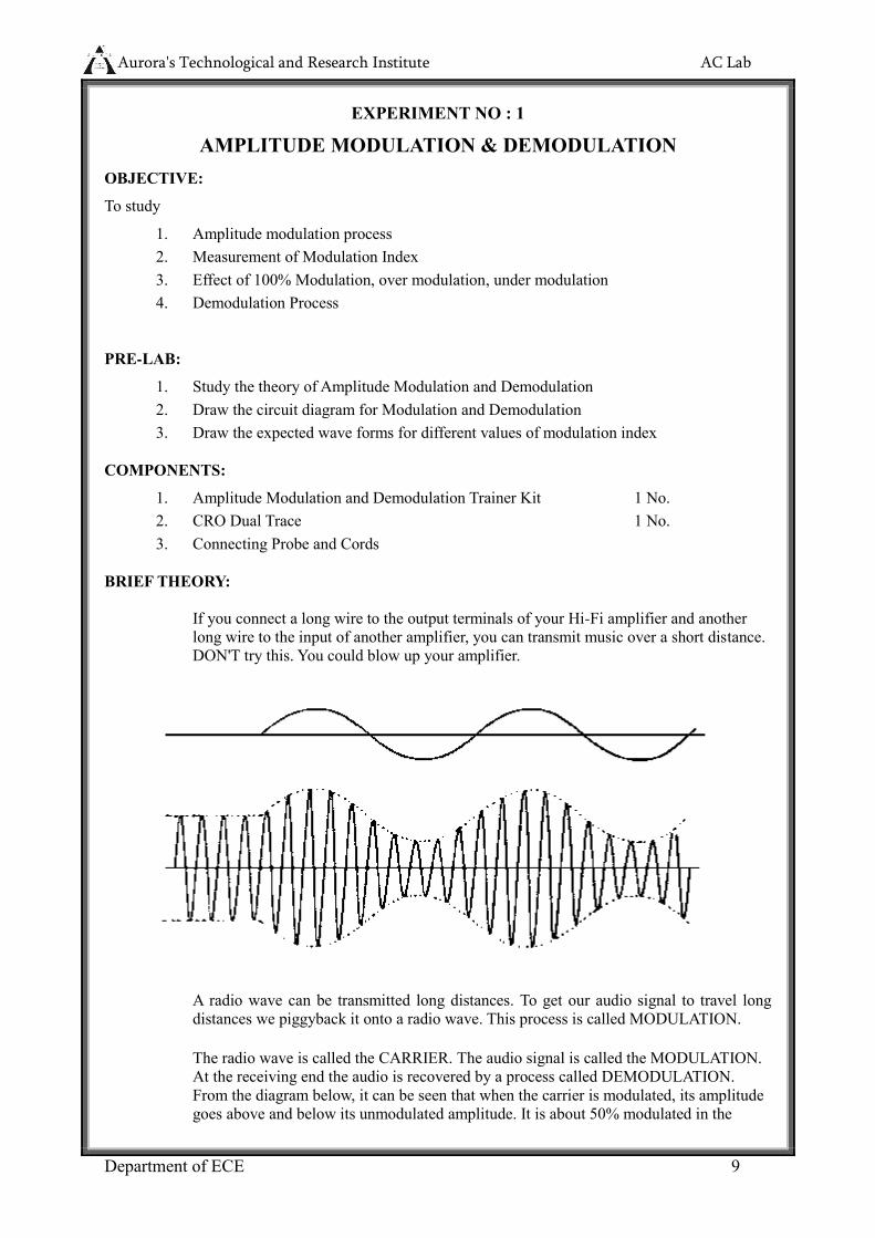
Auroras Technological and Research Institute AC Lab
Department of ECE 9
EXPERIMENT NO 1
AMPLITUDE MODULATION amp DEMODULATION OBJECTIVE
To study
1 Amplitude modulation process
2 Measurement of Modulation Index
3 Effect of 100 Modulation over modulation under modulation
4 Demodulation Process
PRE-LAB
1 Study the theory of Amplitude Modulation and Demodulation
2 Draw the circuit diagram for Modulation and Demodulation
3 Draw the expected wave forms for different values of modulation index
COMPONENTS
1 Amplitude Modulation and Demodulation Trainer Kit 1 No 2 CRO Dual Trace 1 No 3 Connecting Probe and Cords
BRIEF THEORY
If you connect a long wire to the output terminals of your Hi-Fi amplifier and another long wire to the input of another amplifier you can transmit music over a short distance DONT try this You could blow up your amplifier
A radio wave can be transmitted long distances To get our audio signal to travel long distances we piggyback it onto a radio wave This process is called MODULATION
The radio wave is called the CARRIER The audio signal is called the MODULATION At the receiving end the audio is recovered by a process called DEMODULATION From the diagram below it can be seen that when the carrier is modulated its amplitude goes above and below its unmodulated amplitude It is about 50 modulated in the
Auroras Technological and Research Institute AC Lab
Department of ECE 10
diagram The maximum percentage modulation possible is 100 Going above this causes distortion
Most broadcasters limit modulation to 80Modulating the carrier frequency with an audio frequency produces two new frequencies At this point it would be a good idea to read the page on MIXERS These new frequencies are called the upper and lower SIDEBANDS The upper sideband is the carrier frequency plus the audio frequency The lower side band is the carrier frequency minus the audio frequencySince the audio signal is not a single frequency but a range of signals (usually 20 Hz to 20 KHz) the sidebands are each 20Hz to 20 KHz wide
If you tune across a station in the Medium Wave Band you will find that it takes up space in the band This is called the signal BANDWIDTH This is the space taken by the upper and lower sidebands In the the example given above it would be 40 KHz Since the Medium Wave is only 500 KHZ wide there would only be space for about 12 stations Therefore the bandwidth of stations is limited to 9 KHz which limits the audio quality If there are two stations too close together their sidebands mix and produce HETERODYNE whistles Since both sidebands carry
Auroras Technological and Research Institute AC Lab
Department of ECE 11
CIRCUIT DIAGRAMS
AM MODULATION
AM DEMODULATION
CARRIER SIGNAL
TIME T
A
m
p
l i t u
d
e
Ac
Auroras Technological and Research Institute AC Lab
Department of ECE 12
MODULATING SIGNAL
AM MODULATED OUTPUT
AM DEMODULATION OUTPUT
PROCEDURE
A MODULATION i Switch lsquoONrsquo the Trainer Kit
ii Generate the carrier and modulating signal such that carrier frequency must be greater than modulating frequency
iii Apply the carrier and modulating signal into AM modulator input vi Trace the envelope of the modulated waveform
v Repeat step(vi) duly adjusting the modulating signal for under modulation and over modulation
B DEMODULATION
i Apply the modulated AM output into Demodulation input ii Trace the demodulated output waveform
POST- LAB
TIME T
A
m
p
l i t u
d
e
Am
A
m
p
l i t u
d
e
TIME T
Auroras Technological and Research Institute AC Lab
Department of ECE 13
i Observe the frequency and amplitude of the carrier and modulating signal
ii Observe the frequency and maximum peak-peak amplitude(Amax) and minimum peak-
peak amplitude (Amin) of the AM signal in TableI
iii Calculate the modulation index Ч=Amax-AminAmax+Amin
iv Plot the out put waveforms Time T Vs Voltage Vo
v Write result and conclusion
CONCLUSION Hence the AM modulation and demodulation is verified
QUESTIONS 1 what is meant by modulation
2 What is meant by modulation index
3 What is meant by under modulation and over modulation
Auroras Technological and Research Institute AC Lab
Department of ECE 14
EXPERIMENT NO 2
DSB ndash SC Modulator amp Demodulator
OBJECTIVE To study the balanced modulator using IC 1496
PRE-LAB
1 Study the theory of balanced modulator
2 Draw the circuit diagram
3 Draw the expected waveforms
4 Study the datasheet of IC 1496
EQUIPMENT
1 Function generator
2 Dual trace CRO
3 Balanced modulator trainer kit
THEORY
In a balanced modulator a signal is modulated using two carriers that are 180
degrees out of phase The resulting signals are then combined in such a way that the carrier
components cancel leaving a DSB-SC (double sideband suppressed carrier) signal
CIRCUIT DIAGRAM
Auroras Technological and Research Institute AC Lab
Department of ECE 15
BALANCED MODULATOR OUTPUT
Auroras Technological and Research Institute AC Lab
Department of ECE 16
BALANCED DEMODULATOR OUTPUT
PROCEDURE
1 Switch ON the trainer kit
2 Generate the carrier and modulating signal
3 Apply the modulating signal and the carrier signal to the balanced modulator input
4 Observe the balanced modulator output
POST LAB
1 Observe the frequency and amplitude of the carrier and modulating signal
2 Observe the frequency and amplitude of the balanced modulator output
3 Observe the quadrature null effect
4 Plot the output waveforms Time T VS Voltage V
5 Write result and conclusions
CONCLUSIONS The balanced modulator output is verified
QUESTIONS 1 what is the efficiency for DSB SC signal
2 What are the other types of balanced modulators
3 What is meant by pilot carrier
Auroras Technological and Research Institute AC Lab
Department of ECE 17
EXPERIMENT NO 3
SSB ndash SC MODULATOR amp DEMODULATOR
OBJECTIVE To study the Single side band modulation by using Phase shift method and demodulation using synchronous detector method
PRE-LAB
1 Study the theory of SSB
2 Draw the circuit diagram and expected waveforms
EQUIPMENTS 1 Function generator 2
2 Dual trace CRO 1
3 SSB system modulation and demodulation trainer kit 4 Patch CardsConnecting wires
5 Frequency counterMulti meter
THEORY
Single-sideband modulation (SSB) is a refinement of amplitude modulation that more
efficiently uses electrical power and bandwidth It is closely related to vestigial sideband
modulation (VSB)Amplitude modulation produces a modulated output signal that has
twice the bandwidth of the original baseband signal Single-sideband modulation avoids
this bandwidth doubling and the power wasted on a carrier at the cost of somewhat
increased device complexity SSB was also used over long distance telephone lines as part
of a technique known as frequency-division multiplexing (FDM) FDM was pioneered by
telephone companies in the 1930s This enabled many voice channels to be sent down a
single physical circuit for example in L-carrier SSB allowed channels to be spaced
(usually) just 4000 Hz apart while offering a speech bandwidth of nominally 300ndash
3400 Hz Amateur began serious experimentation with SSB after World War II The
Strategic Air Command established SSB as the radio standard for its bombers in 1957[4]
It
has become a de facto standard for long-distance voice radio transmissions since then
Auroras Technological and Research Institute AC Lab
Department of ECE 18
BLOCK DIAGRAM OF SSB MODULATOR
SSB-DEMODULATOR SYSTEM
EXPECTED WAVEFORMS
Auroras Technological and Research Institute AC Lab
Department of ECE 19
DSB-SC 0UTPUT
SSB-SC OUTPUT
PROCEDURE
a Modulation
1 Switch ON the trainer kit 2 Observe the output of RF generator using CROThere are two outputs from the RF
generator one is direct output and another is 90 deg phase shift with the direct output 3 Observe the output of AF generator using CROThere are two outputs from the AF
generator one is direct output and another is 90 deg phase shift with the direct output 4 Set the amplitude of the RF signal to 01vpp and connect the 0 deg phase shift signal to
one BM and 90 deg angle phase shift signal to the second BM
5 Set the AF Signal amplitude to 8vpp and connect to the BM 6 Observe the outputs of both balanced modulators simultaneously and adjust the balance
control until get the output waveforms (DSB SC) 7 To get LSB of SSB connect both balanced modulators outputs to SUBTRACTED circuit 8 Measure the frequencies of LSB using multimeter 9 Calculate the theoretical frequency of the SSB (LSB) and compare it with the practical
value LSB=RE Frequency ndashAF Frequency
10 To get USB of SSB signal connect both balanced modulators outputs to ADDER circuit 11 Measure the frequencies of USB
12 Calculate the theoretical value of the SSB Upper Side Band (SSB-USB) frequency and compare it with practical value
USB=RF Frequency+AF Frequency
Auroras Technological and Research Institute AC Lab
Department of ECE 20
b Demodulation (Synchronous detector)
1 Connect the SSB signal from the summer or sub tractor to the SSB signal input of the synchronous detector and RF signal (0ordm) to the RF input of the synchronous detector
2 Observe the Detector output using CRO and compare it with the AF signal (Modulating Signal)
3 Observe the SSB signal for the different frequencies of the AF signal (modulating signal)
TABULATION RF Frequency (Fc) =--------------------KHz
USB LSB
SNo AFsig
Freq(Fm) Practical Freq Theoretical
Freq=Fc+Fm
Practical Freq
Theoretical Freq=Fc-Fm
POST LAB
1 Observe the frequency and amplitude of the RF carrier both (900 amp 0 0 ) phase AF modulating signal (900 amp 0 0 ) phase DSB-SC SSB-SC LSB and USB of the SSB signal
2 Observe the frequency components and bandwidth of SSB
3 Plot the output waveforms above mentioned 4 Write result and conclusion
CONCLUSIONS Hence various outputs of SSB modulator are obtained
QUESTIONS 1 What are the advantages of SSB over AM
2 What is the main drawback of SSB
3 What is meant by VSB
Auroras Technological and Research Institute AC Lab
Department of ECE 21
EXPERIMENT NO 4
FREQUENCY MODULATION AND DEMODULATION
OBJECTIVE To study
1 Frequency modulation process
2 Measurement of Modulation Index
3 Measurement of Frequency deviation
4 Demodulation Process
PRE-LAB 1 Study the data sheet of IC LM 2206 LM 565
2 Study the theory of FM modulation and demodulation
3 Draw the circuit diagram for modulation and demodulation
4 Draw the expected wave forms
EQUIPMENT 1 Frequency modulation and demodulation trainer kit 1 No 2 Dual trace CRO 1 No 3 Connecting probe and cords
THEORY
In telecommunications frequency modulation (FM) conveys information over a carrier
wave by varying its frequency (contrast this with amplitude modulation in which the amplitude
of the carrier is varied while its frequency remains constant) In analog applications the
instantaneous frequency of the carrier is directly proportional to the instantaneous value of the
input signal Digital data can be sent by shifting the carriers frequency among a set of discrete
values a technique known as keying The instantaneous frequency of the oscillator and is the
frequency deviation which represents the maximum shift away from fc in one direction
assuming xm(t) is limited to the range plusmn1Although it may seem that this limits the frequencies in
use to fc plusmn fΔ this neglects the distinction between instantaneous frequency and spectral
frequency The frequency spectrum of an actual FM signal has components extending out to
infinite frequency although they become negligibly small beyond a point Carsons rule of
thumb Carsons rule states that nearly all (~98) of the power of a frequency-modulated signal
lies within a bandwidth
Auroras Technological and Research Institute AC Lab
Department of ECE 22
CIRCUIT DIAGRAM
MODULATION
DEMODULATION
Auroras Technological and Research Institute AC Lab
Department of ECE 23
OUT PUT WAVEFORMS
Auroras Technological and Research Institute AC Lab
Department of ECE 24
PROCEDURE a Modulation
i Switch ON the trainer kit ii Generate the carrier and modulating signal iii apply the modulating signal to the frequency modulator iv Trace the FM output
b Demodulation i apply the modulated FM output into Demodulation input ii Trace the demodulated output waveform
TABULATION
SNo
Amplitude of Modulating
Signal(Am) Fmin
Frequency
Deviation
∆f=fc-fmin or fc-fmax
Modulation Index β=∆ffm
POST LAB
1 Observe the frequency and amplitude of the carrier and modulating signal 2 Calculate the frequency deviation by observing Fmax and Fmin
δ=Fc-Fmax or δ=Fc-Fmin
3 Calculate modulation index β= δFm
4 Change the amplitude of the modulating signal and repeat steps 1 to 3 for different values of Am and note down the readings in table-1
5 Plot the output waveforms Time T VS Voltage Vo
6 Write result and conclusion
CONCLUSIONS Hence the frequency modulated output is obtained
QUESTIONS 1 what is meant by angle modulation
2 How FM is different from AM
3 What is meant by Carson Rule
4 What is the maximum modulation index
Auroras Technological and Research Institute AC Lab
Department of ECE 25
EXPERIMENT NO 5
STUDY OF SPECTRUM ANALIZER AND ANALYSIS OF AM amp FM SIGNALS
Auroras Technological and Research Institute AC Lab
Department of ECE 26
Auroras Technological and Research Institute AC Lab
Department of ECE 27
Auroras Technological and Research Institute AC Lab
Department of ECE 28
EXPERIMENT NO 6
PRE EMPHASIS AND DE EMPHASIS
OBJECTIVE To study the operation of Pre-emphasis and De-emphasis circuits
PRE-LAB
1 Study the theory of Pre-emphasis and De-emphasis circuits
2 Draw the circuit diagram
3 Draw the expected waveforms
COMPONENTS
1 Resistors 100kΩ 100Ω
2 Capacitors 1μf 100μf EQUIPMENT 1 Function generator 1
2 Dual trace CRO 1
THEORY Pre-emphasis
Improving the signal to noise ratio by increasing the magnitude of higher frequency
signals with respect to lower frequency signals
De-emphasis
Improving the signal to noise ratio by decreasing the magnitude of higher
frequency signals with respect to lower frequency signals
Transmitters that employ a true FM modulator require a pre emphasis circuit before the
modulator fore the true FM modulator doesnt automatically pre emphasize the audio like
a transmitter that uses a phase modulator A separate circuit is not necessary for pre
emphasis in a transmitter that has a phase modulator because the phase modulator applies
pre emphasis to the transmitted audio as a function of the phase modulator The receivers
De emphasis circuitry takes the unnatural sounding pre emphasized audio and turns it
back into its original response Pre emphasized (discriminator) audio is however available
directly from the audio demodulation (discriminator) circuitry In linking systems many
choose to eliminate the emphasis circuitry to allow better representation of retransmitted
Auroras Technological and Research Institute AC Lab
Department of ECE 29
signals Since the signal has already been pre emphasized (by the user that is
transmitting) and since the receiver you are listening to takes care of the de emphasis
CIRCUIT DIAGRAMS
PRE-EMPHASIS
DE-EMPHASIS
EXPECTED WAVEFORMS
INPUT
TIME T
A
m
p
l i t u
d
e
Am
Auroras Technological and Research Institute AC Lab
Department of ECE 30
OUTPUT
PRE-EMPHASIS
Freq Vs Gain
DE-EMPHASIS
Freq Vs Gain
TIME T
Freq f (Hz)
A
m
p
l i t u
d
e
Am
Auroras Technological and Research Institute AC Lab
Department of ECE 31
TABLE
PRE EMPHASIS
SNo Input Freq
Input Voltage Vi (Volts)
Output Voltage Vo (Volts) Gain=VoVi
Gain in dB
20log(voVi)
DE-EMPHASIS
SNo Input Freq
Input Voltage Vi (Volts)
Output Voltage Vo (Volts)
Gain=VoVi Gain in dB
20log(VoVi)
PROCEDURE a Pre-emphasis
1 Connect the circuit as per the circuit diagram
2 Apply a constant sine wave input across the input terminal of fixed amplitude(Vi) 3 By varying the input frequency note down the output amplitude (Vo) with respect to
input frequency in Table 4 Calculate the gain using the formula
5 Gain =20log (Vo) (Vi) db
b De-Emphasis
1 Connect the circuit as per the circuit diagram
2 Repeat the steps 2 3 amp4
POST LAB
1 Observe the output amplitude for both the pre-emphasis and De-emphasis circuits
2 Calculate the gain in db
3 Plot the frequency versus gain curves on logarithmic graphs for both the circuits
4 Plot the input and output waveforms Time T VS Voltage Vo
5 Write the result and conclusion
CONCLUSIONS Obtained the pre emphasis and de-emphasis outputs
QUESTIONS 1 Observe the out put signal is disturbed by noise what action has to be taken and measure the
output voltage 2 Where we use the pre emphasis circuit 3 Where we use the de emphasis circuit 4 What are the advantages of pre emphasis and de emphasis circuits
Auroras Technological and Research Institute AC Lab
Department of ECE 32
EXPERIMENT NO 7
TIME DIVISION MULTIPLEXING AND DEMULTIPLEXING
AIM To study Time Division Multiplexing and its waveforms
PRE LAB WORK
Study the operation of Time division multiplexer and demultiplexer Draw the block diagram of TDM
Draw the expected graphs of all necessary waveforms ( CH1CH2TDM OP and Demultiplexed OP)
EQUIPMENT
1) Experimental board on TDM
2) Dual Trace CRO 3) Probes
THEORY
Time Division Multiplexing (TDM) is a technique for transmitting serial messages on a signal
transmission channel by dividing the time division into slots One slot for each message The concept
of TDM comes from sampling theorem which enables use to transmit the information contained in the
band limited Signal using sampling of the signal taken uniformly or a rate slightly higher then the
Nyquist rate TDM enables the joint utilization at a common transmission channel by a number of
independent message sources without mutual interference
The different Ip message signals all band limited in WHz by the IP low pass filters and sequentially
sampled at the transmitters by a rotary switch or a comparator The switch makes are complete
revolution in Ts frac12 W extracting are sample from each IP The commutator OP is a PAM waveform
containing individual message sample
It there are N number of IP the pulse to Pulse spacing will be Ts = 1 while the spacing
N Nfs
bw successive samples from each IP is called a frame
At the receiver a similar rotatory switch the decommutator separates the samples and distributes them
to a bank of low-pass filters which in turn is usually electronic and synchronization signals are
provided to keep the distribute in step with the commutant
Auroras Technological and Research Institute AC Lab
Department of ECE 33
EXPECTED GRAPHS
PROCUDURE
1 Connect the OP of the experimental board to one of the channels on CRO 2 Switch ON the experimental board 3 Observe the OP waveforms 4 Vary the values of the resistors R1 R2 and R3 alternative and observe the OP on CRO
RESULT
The process of the Time Division Multiplexing and the waveforms has been studied
CONCLUSION
Auroras Technological and Research Institute AC Lab
Department of ECE 34
Figure 1 Time Division Multiplexing amp De multiplexing
Auroras Technological and Research Institute AC Lab
Department of ECE 35
EXPERIMENT NO 9
VERIFICATION OF SAMPLING THEOREM
AIM To study the effect of sampling on the transmission of information through PWM
PRE LAB WORK
Study the sampling theorem
Draw the expected graphs of all necessary waveforms ( message signal carrier wave PWM op demodulated op etc
EQUIPMENT
1) Experimental Board on study of sampling theorem 2) Dual trace CRO (0 ndash 20 MHz) 3) Function Generator 4) Connecting wires
THEORY
The principle of sampling can be explained using the switching sampler The switch periodically shifts below bw two constants at the rate of fs = 1 Ts Hz staying on the IP constant for each sampling period The op Xs(t) of the samples consists of segments of x(t) and Xc(t) can be represented as
Xs(t) = X(t) S(t)
Where S(t) is sampling or switching function There are a number of differences bw the ideal sampling and reconstruction techniques described in the proceeding sections of the actual signal
PROCEDURE
1) Observe the internal clock and measure its frequency and amplitude 2) Give the clock to the clock IP terminal 3) Connect the modulating signal to the IP 4) Check the condition fs gt 2fm and observe the de-modulated wave 5) Check the condition fs lt 2fm and fs = 2fm and draw the OP waveforms
RESULT
CONCLUSION
Aurorarsquos Technological and Research Institute DC Lab
36
Figure 2 Sampling Theorem
Aurorarsquos Technological and Research Institute DC Lab
37
EXPERIMENT NO 10
PULSE AMPLITUDE MODULATION AND DEMODULATION
AIM 1) To study the PAM modulation and its waveforms
2) To study the de-modular of PAM
3) To study the effect of sampling frequency on de-modulation OP
PRE LAB WORK
Study the operation Pulse Amplitude Modulator and Demodulator Draw the block diagram of PAM modulator and demodulator Draw the expected graphs of all necessary waveforms ( message signal carrier wave PAM op
demodulated op etc)
EQUIPMENT
1) Exp Board on study of PAM 2) CRO 3) Functional Generator 4) Connecting wires and chords
THEORY
In PAM the amplitude of the carrier wave of higher frequency follow the amp of the message signal
Within this (Modulation Sampling) we have two more types of sampling those are
(1) Natural Sampling
(2) Flat Top Sampling
Basically in Natural Sampling the carrier waves are train of pulses of a certain frequency After
sampling the top of the Pulse follow the message signal Due to this following of top of Pulses with the
message signals cause a distortion in De-modulation
In Flat top sampling also we use train of pulses for sampling but only the starting point of each pulse
follow the message signal remaining width of the pulse will (follow) be flat But here we go for Natural
sampling
EXPECTED WAVEFORMS
Aurorarsquos Technological and Research Institute DC Lab
38
PROCEDURE (MODULATION)
1 Observe the clock on CRO and measure its frequency and amp (freq 5KHz) 2 Connect the clock to clock IP terminals in modulation 3 Put control switch in ac position and set amplitude = OV This provides DC at Modulating
signal terminal 4 Connect the modulating signal or IP to the modulator 5 Connect one channel of CRO at lsquoTirsquo and Gnd Observe that the pulses are of same height
Height is adjustable by varying offset This is PAM signal with DC IP Measure amplitude and frequency of Pulses
6 Increase the amplitude of modulation signal Observe the amplitude and frequency of this sinusoidal modulating signal
7 Observe PAM signal
a) How many Pulses are there in one modulating cycle
b) It is natural or Flat Top PAM c) It is Single or dual polarity PAM
8 Observe the effect of DC offset on PAM waveform
DE-MODULATION
1) Generate undistorted PAM waveform 2) Connect the modulating signal to de-modulation IP 3) Observe the detected OP and measure its frequency which must be same as
modulating signal
EFFECT OF SAMPLING FREQUENCY
1) Connect internal sinusoidal signal to modulating signal IP of the modulator 2) Connect an external functional Generator at the circuit terminals of the modulator 3) Get the PAM waveform using the above circuit 4) Adjust the modulating amplitude offset and frequency to get an undistorted frequency 5) Connect the PAM to de-modulator IP 6) Observe the demodulated signal for various frequencies of clock (fs gt 2fm lt 2fm = 2 fm)
RESULT
CONCLUSION
Aurorarsquos Technological and Research Institute DC Lab
39
Figure 3 Pulse Amplitude Modulation
Auroras Technological and Research Institute AC Lab
Department of ECE 5
EXPERIMENT NO 11
PULSE WIDTH MODULATION AND DEMODULATION
AIM
1) To study the PWM process and the corresponding waveforms 2) To study the effect of sampling frequency on the transmission of information through PWM
PRE LAB WORK
Study the operation Pulse Width Modulator and Demodulator Draw the block diagram of PWM modulator and demodulator Draw the expected graphs of all necessary waveforms ( message signal carrier wave PWM op
demodulated op etc
EQUIPMENT
1) Experimental Board
2) Dual trace CRO 3) AF generator 4) Multimeter
THEORY
In PWM the samples of the message signal are used to vary the duration of the individual pulses The
pulse width may be varied by varying the time of occurrence of the leading edge trailing edge of both
edges of the pulse in accordance with the sampled value of the modulating wave PWM can also be
generated by using emitter follower monostable multivibrator is an excellent voltage to time converter
since its gate width is dependent on the voltage to which the capacitor is changed If this voltage can be
varied in accordance with a signal voltage a series of rectangular pulses can be obtained with width
varying as required
The demodulated of PWM is quite simple PWM is passed through a low pass filter The reconstruction is
associated with a certain amount of Distortion caused by the cross modulator products that fall in the
signal band
EXPECTED WAVEFORM
Aurorarsquos Technological and Research Institute DC Lab
41
PROCEDURE
STUDY OF MODULATION
1) Observe the clock on CRO and measure its frequency (fs) 2) Observe the sine wave modulating signal on CRO and observe the dc shift produced in this
by varying the offset nob Measure the frequency Variation limits of this signal 3) Apply clock at the circuit input terminal 4) Apply modulating signal by keeping the control switch in dc position 5) Observe the modulated wave 6) Plot the graph bw pulse width and the applied dc voltage 7) Put the control switch in sine wave position and adjust the modulating signal amplitude
frequency and dc offset to get the stationary waveform of PWM 8) Note the number of pulses in one circuit of modulating signal
STUDY OF DEMODULATION
1) Generate the stationary PWM waveform using sin wave modulating signal 2) Connect the modulator OP to PWM demodulator 3) Connect Channel (1) to Modulating Signal and channel (2) to demodulated wave
EFFECT OF SAMPLING FREQUENCY
1) Use an external square wave and connect it to the clock input 2) Set the frequency of square wave at frequency 2fm 3) Observe the demodulated wave
4) Change the frequency of square wave to fs lt 2fm fs gt 2fm and observe the demodulated wave
RESULT
CONCLUSION
Aurorarsquos Technological and Research Institute DC Lab
42
Figure 4 Pulse Width Modulation
Aurorarsquos Technological and Research Institute DC Lab
43
EXPERIMENT NO 12
PULSE POSITION MODULATION AND DEMODULATION
AIM
1) To study the PPM Modulation and the corresponding waveforms 2) To study the de-modulation of PPM 3) To see the effect of sampling frequency on the transmission of information through PPM
PRE LAB WORK
Study the operation Pulse Position Modulator and Demodulator Draw the block diagram of PPM modulator and demodulator Draw the expected graphs of all necessary waveforms ( message signal carrier wave PPM op
demodulated op etc
EQUIPMENT
1) Experimental Board for PPM
2) Dual Phase Oscilloscope
3) AF Generator
THEORY
In PDM long pulses expand considerable power duration If the pulse which bearing no additional
information If this un used power is subtracted from PDM so that only time transitions are preserved
We observe a more efficient type of pulse modulation known as pulse position modulation Here in the
Pulse Position Modulated wave the position of the Pulse relative to its unmodulated time of occurrence is
varied in accordance with the message signal
We generate a PPM wave from PWM wave by using a Monostable Multivibrator The device has one
absolutely stable state and one quest ndash stable state into which it is triggered by an externally applied Pulse
The monostable multivibrator is designed to trigger on the trailing edges of the duration ndash modulated pulse
is varied in accordance with the message signal
The fixed pulse duration of the PPM wave at the monostable multivibrator OP can be set by appropriately
choosing the resistance ndash capacitance combination in the timing circuit of the device
Aurorarsquos Technological and Research Institute DC Lab
44
EXPECTED WAVEFORM
PROCEDURE
STUDY OF MODULATION
Observe the clock and measure its frequency (fs) Apply the clock at the clock IP terminal in the modulator Apply the modulating signal keeping control switch in DC position Observe the PPM OP Connect the channel ndash (1) on CRO to clock and channel (2) to PPM wave OP Compare the position of two waveforms Vary the DC offset and observe the relative shift between the clock and PPM OP Measure the time shift between clock and PPM wave for various settings of offset Draw the graph between time shift and DC voltage Put the control switch in AC position adjusts the amplitude and frequency and offset
of sinusoidal modulating signal to get the stationary PPM wave Note the number of pulses in one cycle of the modulated wave
STUDY OF DEMODULATION
Generate a stationery PPM wave for a sinusoidal modulating signal Apply the PPM wave to the input of de-modulator Connect the Channel ndash (1) of CRO to the modulating signal and channel ndash 2 to the
de-modulator output Compare the two waveforms
Note the frequency of demodulated wave It should be same as the modulating signal Note down the waveform
RESULT
CONCLUSION
Aurorarsquos Technological and Research Institute DC Lab
45
Aurorarsquos Technological and Research Institute DC Lab
46
Figure 5 Pulse Position Modulation
Aurorarsquos Technological and Research Institute AC Lab
47
EXPERIMENT NO 13
FREQUENCY SYNTHESIZER
AIM
To study the operation of frequency synthesizer using PLL
PRE-LAB 1 Study the data sheet of IC 7404IC 4017IC 565 and IC 4046
2 Study the theory of frequency synthesizer 3 Draw the circuit diagram and expected waveforms
EQUIPMENTS
1 Frequency synthesizer trainer AET -26A
2 Dual trace CRO (20Mhz) 3 Digital frequency counter or multimeter
4 Patch chords
THEORY
A frequency synthesizer is an electronic system for generating any of a range
of frequencies from a single fixed time base or oscillator They are found in many modern
devices including radio receivers mobile telephones radiotelephones walkie-talkies CB
radios satellite receivers GPS systems etc A frequency synthesizer can combine
frequency multiplication frequency division and frequency mixing (the frequency mixing
process generates sum and difference frequencies) operations to produce the desired output
signal
BLOCK DIAGRAM
Phase Comparator
Amplifier Low pass filter
V C O
Div N Network frequency divider
Fin= fout
N
fin
Fout =Nf in
Aurorarsquos Technological and Research Institute AC Lab
48
SIMPLE 1KHZ-9KHZ FREQUENCY SYNTHESIZER
CIRCUIT DAIGRAM
PROCEDURE 1 Switch on the trainer ad verify the output of the regulated power supply ie 5V These
supplied are internally connected to the circuit so no extra connections are required 2 Observe output of the square wave generator using oscilloscope and measure the range
with the help of frequency counter frequency range should be around 1KHz to 10KHz 3 Calculate the free running frequency range of the circuit (VCO output between 4th pin
and ground 1 For different values of timing resistor R1 ( to measure Rt value using digital multimeter between given test points 1 And record the frequency values in table 1
Fout = 03 (RtCt) where Rt is the timing resistor and Ct is the timing capacitor = 001 f
Aurorarsquos Technological and Research Institute AC Lab
49
4 Connect 4th pin of LM 565 (Fout) to the driver stage and 5th pin (Phase comparator) connected to 11th pin of 7404 Output can be taken at the 11th pin of the 7490 It should be divided by the 2 amp 3 times of the fout
TABULATION
Fin KHz Fout = N x fin KHz Divided by 3 2
EXPECTED WAVEFORMS
POST LAB
1 Observe the synthesized output in table 2 Calculate the output frequency
3 Plot the output waveforms
4 Write result and conclusions
CONCLUSIONS
The various outputs of frequency synthesizer are verified
QUESTIONS
1 What are the applications of frequency synthesizer
TIME T
A
m
p
l i T
u
d
e
Ac
Aurorarsquos Technological and Research Institute AC Lab
50
2 What is the difference between heterodyning and synthesizer
Aurorarsquos Technological and Research Institute AC Lab
51
EXPERIMENT NO 14
AGC CHARATERISTICS
AIM
To observe the effect of automatic gain control(AGC)
PRE LAB 1 To study the theory of AGC 2 Draw the Block Diagram circuits diagram and expected waveforms
EQUIPMENTS 1 AGC Trainer Kit 2 CRO
3 Patch Chords
4 Digital Multimeter
THEORY
Automatic gain control (AGC) is an adaptive system found in many electronic
devices The average output signal level is fed back to adjust the gain to an appropriate level
for a range of input signal levels For example without AGC the sound emitted from an AM
radio receiver would vary to an extreme extent from a weak to a strong signal the AGC
effectively reduces the volume if the signal is strong and raises it when it is weaker AGC
algorithms often use a PID controller where the P term is driven by the error between
expected and actual output amplitude
Block Diagram
Frequency Converter
1st IF Amplifier
2nd IF Amplifier
Detector
Audio Preamplifier
Driver Output
Aurorarsquos Technological and Research Institute AC Lab
52
CIRCUIT DIAGRAM
PROCEDURE
1 Connect 455 KHz IF Signal Function Generator connect AGC link Connect CRO channel-1 at input terminals
2 Connect CRO channel 2 at collector of Q3 The amplified signal will be observed 3 Calculate the voltage gain by measuring the amplitude of output signal (Vo) waveform
using formula A=VoVi 4 Now connect CRO-2 channel at output The detected audio signal of 455 Khz will be
observed 5 Now vary input level of 455 KHz IF signal and observe detected 455 KHz audio signal
with and without AGC link The output will be distorted when AGC link is removed ie there is no AGC action
6 This explains AGC effect in Radio circuit
TABULATION
SNo Input Voltage Vi (P-P) With out AGC With AGC
Output Voltage Vo (P-P)
Gain A= Vo Vi
Output Voltage Vrsquoo (P-P)
Gain Arsquo= Vrsquoo Vi
Aurorarsquos Technological and Research Institute AC Lab
53
EXPECTED WAVEFORMS
AM Modulated RF Input
Detected Output with AGC
Detected Output without AGC
POST-LAB
1 Observe the input voltage and output voltage for with AGC and Without AGC in Table 1
2 Calculate Gain a=vovi for both cases 3 Plot the output waveforms Time T Vs Voltage Vo and input voltage Vi Vs Gain A 4 Write Result and Conclusions
CONCLUSIONS The AGC characteristics are verified
QUESTIONS 1 what is meant by AGC
2 What is the difference between simple AGC and delayed AGC
3 From which part of receiver AGC is obtained
TIME T
A
m
p
l i T
u
d
e
Ac
TIME T
A
m
p
l i T
u
d
e
Ac
TIME T
A
m
p
l i T
u
d
e
Ac
Aurorarsquos Technological and Research Institute AC Lab
54
EXPERIMENT NO 15
PHASE LOCKED LOOP
OBJECTIVE To study the Phase locked loop using 565 IC and to take input frequency given by an external signal source
PRE-LAB To Study
1 The data sheet of IC 565
2 The theory of Phase locked loop
3 About free running frequency locking range and capture range
4 Draw the circuit diagram and expected waveforms
EQUIPMENT 1 Function generator 2
2 Dual trace CRO 1
3 Phase locked loop trainer kit
THEORY
A phase-locked loop or phase lock loop (PLL) is a control system that generates a signal
that has a fixed relation to the phase of a reference signal A phase-locked loop circuit
responds to both the frequency and the phase of the input signals automatically raising or
lowering the frequency of a controlled oscillator until it is matched to the reference in both
frequency and phase A phase-locked loop is an example of a control system using negative
feedback Phase-locked loops are widely used in radio telecommunications computers and
other electronic applications They may generate stable frequencies recover a signal from a
noisy communication channel or distribute clock timing pulses in digital logic designs
such as microprocessors Since a single integrated circuit can provide a complete phase-
locked-loop building block the technique is widely used in modern electronic devices
with output frequencies from a fraction of a cycle per second up to many gigahertz
BLOCK DIAGRAM
Aurorarsquos Technological and Research Institute AC Lab
55
CIRCUIT DIAGRAM
PROCEDURE 1 Switch ON the trainer kit 2 Check the VCO output at pin 4 of IC 565 that is a square wave form The frequency of the
VCO Output depends on CT (001f) and RT (47kΩ) 3 Next short the pins 4amp5 and give signal of variable frequency and observe VCO output 4 Change the input frequency and observe the VCO output on the CRO 5 Between some frequencies the VCO output is locked to the input signal frequency This can
be observed by increasing or decreasing the frequency of the VCO output by changing input frequency
6 Before or after that frequency range the VCO output is not locked
7 Calculate Lock range (FL) and capture range (FC) by using the following formulas
FL = 8foVCO fo=03RtCT
FC=12π radic2πf236103 C2
Table1
SNo Locking Frequency Frequency Range From To
CHARTERISTICES
Aurorarsquos Technological and Research Institute AC Lab
56
CONCLUSIONS Obtained the lock range of PLL
QUESTIONS
1 Observe the VCO output when pins 4amp5 short and give square wave as signal 2 Define lock range and capture range
3 What are the basic applications of PLL
Aurorarsquos Technological and Research Institute AC Lab
57
ANNEXURE-I
EXPERIMENT NO 1
Aurorarsquos Technological and Research Institute AC Lab
58
CHARACTERISTICS OF MIXER
AIM
To study the functioning of a frequency mixer
PRE LAB 1 To study the theory of Mixer 2 Draw the circuit diagram and expected waveforms
EQUIPMENTS 1 Frequency mixer trainer kit 2 CRO (20MHz) 3 Connecting cords and probes 4 Function generator (1MHz)
THEORY
In receivers using the super heterodyne principle a signal at variable frequency is
converted to a fixed lower frequency IF before detection IF is called the intermediate frequency
In typical AM (Amplitude Modulation eg as used on medium wave) home receivers that
frequency is usually 455 kHz for FM VHF receivers it is usually 107 MHz An intermediate
frequency (IF) is a frequency to which a carrier frequency is shifted as an intermediate step in
transmission or reception Frequency modulation (FM) is a form of modulation that represents
information as variations in the instantaneous frequency of a carrier wave Very high frequency
(VHF) is the radio frequency range from 30 MHz (wavelength 10 m) to 300 MHz (wavelength 1
heterodyne receivers mix all of the incoming signals with an internally generated waveform
called the local oscillator The user tunes the radio by adjusting the sets oscillator frequency in
the mixer stage of a receiver the local oscillator signal multiplies with the incoming signals
which shifts them all down in frequency The one that shifts is passed on by tuned circuits
amplified and then demodulated to recover the original audio signal The oscillator also shifts a
copy of each incoming signal up in frequency by amount Those very high frequency images
are all rejected by the tuned circuits in the IF stage The Super heterodyne receiver (or to give it its
full name The Supersonic Heterodyne Receiver usually these days shortened to superhet) was
invented by Edwin Armstrong in 1918
Aurorarsquos Technological and Research Institute AC Lab
59
BLOCK DIAGRAM
CIRCUIT DIAGRAM
EXPECTED WAVEFORMS
INPUT SIGNAL Fx
INPUT SIGNAL Fy
TIME T
A
m
p
l i T
u
d
e
Ac
Aurorarsquos Technological and Research Institute AC Lab
60
MIXER OUTPUT(Fy-Fx)
PROCEDURE 1 Connect the circuit as per the given circuit diagram 2 Switch on the power supply of trainer kit 3 Apply a sine wave at input Fx of 2 VP-P amplitude and 100 KHz frequency 4 Apply a sine wave at input FY of 2 VP-P amplitude and 100 KHz frequency 5 Observe the output waveform on the CRO 6 Repeat the steps 34 and 5 by changing the values of Fx once greater than and less than
FY in a steps of 5Khz (in the range 80KHz to 120KHz)
TABULATION
TIME T
A
M
P
L
I T
U
D
E
TIME T
A
m
p
l i T
u
d
e
Ac
Aurorarsquos Technological and Research Institute AC Lab
61
SNo Freq (Fy)
(kHz) Amp(V) Freq(Fx) (kHz) Amp(V) Freq(Fy-Fx)
(kHz) Amp(V)
POST LAB 1 Observe the amplitude and time Of inputs and output in table
2 Draw the expected waveforms
3 Verify the output signal obtained with the theoretical value 4 Plot the graphs for Time T VS input signal (FX) Voltage V input signal (FY) Voltage V
and output Signal F(x-y) voltage V 5 Write result and conclusions
CONCLUSIONS
Obtained the output of the mixer for various inputs
QUESTIONS
1 what are the different types of mixtures available
2 What is meant by heterodyning
3 What is meant by IF
Aurorarsquos Technological and Research Institute AC Lab
62
EXPERIMENT NO 2
DIGITAL PHASE DETECTOR
OBJECTIVE To detect the phase difference between two square wave signals using digital phase detector
PRE LAB
1 To study the theory of digital phase detector and EX-OR gate operation and truth table 2 Draw the circuit diagram and expected output and input waveforms
EQUIPMENT 1 Digital phase detector trainer kit 2 Regulated power supplies
3 CRO (20MHz) 4 Connecting cords amp probes
5 Digital frequency counter or multimeter
THEORY
Phase detector is a frequency mixer or analog multiplier circuit that generates a voltage
signal which represents the difference in phase between two signal inputs It is an essential
element of the phase-locked loop (PLL)Detecting phase differences is very important in many
applications such as motor control radar and telecommunication systems servo mechanisms and
demodulators
Electronic phase detector
Some signal processing techniques such as those used in radar may require both the amplitude
and the phase of a signal to recover all the information encoded in that signal One technique is to
feed an amplitude-limited signal into one port of a product detector and a reference signal into the
other port the output of the detector will represent the phase difference between the signals If the
signal is different in frequency from the reference the detector output will be periodic at the
difference frequency Phase detectors for phase-locked loop circuits may be classified in two
types A Type I detector is designed to be driven by analog signals or square-wave digital signals
and produces an output pulse at the difference frequency The Type I detector always produces an
output waveform which must be filtered to control the phase-locked loop variable frequency
oscillator (VCO) A type II detector is sensitive only to the relative timing of the edges of the input
and reference pulses and produces a constant output proportional to phase difference when both
signals are at the same frequency This output will tend not to produce ripple in the control voltage
of the VCO
Aurorarsquos Technological and Research Institute AC Lab
63
BLOCK DIAGRAM OF PLL
CIRCUIT DIAGRAM
Aurorarsquos Technological and Research Institute AC Lab
64
EXPECTED WAVEFORMS
EX-OR PHASE DETECTOR
EDGE TRIGGERED OUTPUT
PROCEDURE
1 Switch on the trainer kit
2 Observe the output of the square wave generator available on the trainer kit using CRO
and measure the range with the help of frequency counter the frequency range should be
around 2 KHz to 13 KHz
3 Calculate the free running range of the VCO output ie between 4th pin of IC PLL 565
and ground For different values of timing resistor Rt fout is given by Fout =03 Rt Ct
where Ct timing capacitor = 001 μF Rt timing resistor
4 Connect the square wave to the input of IC PLL 565 and short 4th and 5th pin of PLL
Vary the input frequency of the square wave when the PLL is locked that is connected to
Aurorarsquos Technological and Research Institute AC Lab
65
one input fout EX-OR phase detector The other input fin of EX-OR phase detector is the
coming from inbuilt of square wave generator
5 Connect the pulse generator output to the input of IC 565 PLL and short 4th amp 5th pin of
PLL Vary the input frequency of the square wave when the PLL is locked that is
connected to one input of Edge triggered phase detector input ie fout The other input fin
of edge triggered phase detector is the pulse input coming from the inbuilt pulse generator
6 The dc output voltage of the exclusive-OR phase detector is a function of the phase
difference between its two inputs fin and fout
POST LAB
1 Observe the Voltage and Time of the two input square waves
2 Observe difference of two inputs as square wave output
3 Plot the inputs and output waveforms Time T VS Voltage V
CONCLUSIONS
The phase detector outputs are verified
QUESTIONS
1 What is the function of phase detector
2 What is the condition for getting maximum output
3 Advantages of digital phase detector over analog phase detector
Aurorarsquos Technological and Research Institute AC Lab
66
EXPERIMENT NO 3
COASTAS RECEIVER
AIM
To demodulate a DSB-SC signal using coastas receiver
PRE LAB 1 To study the operation of coastas receiver 2 Draw the circuit diagram and expected waveforms
EQUIPMENTS 1 Communications trainer kit 2 DSB-SC modulator trainer kit 3 CRO (20MHz) 4 Connecting cords and probes 5 Function generator (1MHz)
THEORY
This loop and its variations is much-used as a method of carrier acquisition (and
simultaneous message demodulation) in communication systems both analog and digital
It has the property of being able to derive a carrier from the received signal even when there is
no component at carrier frequency present in that signal (eg DSBSC) The requirement is that
the amplitude spectrum of the received signal be symmetrical about this frequency
The Costas loop is based on a pair of quadrature modulators - two multipliers
fed with carriers in phase-quadrature These multipliers are in the in-phase (I) and quadrature
phase (Q) arms of the arrangement Each of these multipliers is part of separate synchronous
demodulators The outputs of the modulators after filtering are multiplied together in a third
multiplier and the lowpass components in this product are used to adjust the phase of the local
carrier source - a VCO - with respect to the received signal The operation is such as to
maximise the output of the I arm and minimize that from the Q arm The output of the I arm
happens to be the message and so the Costas loop not only acquires the carrier but is a
(synchronous) demodulator as well A complete analysis of this loop is non-trivial It would
include the determination of conditions for stability and parameters such as lock range capture
range and so on
Aurorarsquos Technological and Research Institute AC Lab
67
BLOCK DIAGRAM
EXPECTED WAVEFORMS
DSB-SC modulated output
Aurorarsquos Technological and Research Institute AC Lab
68
Demodulated output of the coastas loop
PROCEDURE
1 Switch ON the DSB-SC trainer kit
2 Generate the carrier and modulating signal
3 Generate the DSB-SC modulated signal
4 Connect the required blocks of the coastas receiver in the communications kit
5 Apply the generated DSB-SC signal to the above connected coastas receiver
6 Observe that the output of the coastas receiver is the demodulated wave of DSB-SC signal
POST LAB
1 Observe the frequency and amplitude of the carrier and modulating signal
2 Observe the frequency and amplitude of the balanced modulator output
3 Observe the lock condition of the coastas loop
4 observe the output of the coastas demodulator
5 Write result and conclusions
CONCLUSIONS The balanced modulator output and the operation of coastas receiver is verified
QUESTIONS 1 what is the operation of coastas loop
2 What happens when the locking condition of the coastas loop occurs
3 Coastas loop can be used for demodulation of other modulation techniques also What are they
Aurorarsquos Technological and Research Institute AC Lab
69
MATLAB PROGRAMMES
Aurorarsquos Technological and Research Institute AC Lab
70
INDEX
1 Introduction - 70
2 Amplitude Modulation and Demodulation - 74
3 DSB-SC Modulation and Demodulation - 84
4 SSB-SC Modulation and Demodulation - 89
5 Frequency Modulation and Demodulation - 95
6 Phase Modulation and Demodulation - 99
7 Time Division Multiplexing and Demultiplexing - 100
8 Frequency Division Multiplexing and Demultiplexing- 103
9 Verification of Sampling Theorem - 104
10 Pulse Amplitude Modulation and Demodulation - 106
11 Pulse width Modulation and Demodulation - 108
12 Pulse Position Modulation and Demodulation - 110
13 PLL as FM Demodulator - 112
Aurorarsquos Technological and Research Institute AC Lab
71
1 INTRODUCTION
What Is Simulink
Simulink is a software package for modeling simulating and analyzing dynamic
systems It supports linear and nonlinear systems modeled in continuous time sampled time
or a hybrid of the two Systems can also be multirate ie have different parts that are
sampled or updated at different rates
Tool for Simulation
Simulink encourages you to try things out You can easily build models from scratch
or take an existing model and add to it You have instant access to all the analysis tools in
MATLABreg so you can take the results and analyze and visualize them A goal of Simulink
is to give you a sense of the fun of modeling and simulation through an environment that
encourages you to pose a question model it and see what happens
Simulink is also practical With thousands of engineers around the world using it to
model and solve real problems knowledge of this tool will serve you well throughout your
professional career
Tool for Model-Based Design
With Simulink you can move beyond idealized linear models to explore more realistic
nonlinear models factoring in friction air resistance gear slippage hard stops and the other
things that describe real-world phenomena Simulink turns your computer into a lab for
modeling and analyzing systems that simply wouldnt be possible or practical otherwise
whether the behavior of an automotive clutch system the flutter of an airplane wing the
dynamics of a predator-prey model or the effect of the monetary supply on the economy
For modeling Simulink provides a graphical user interface (GUI) for building models
as block diagrams using click-and-drag mouse operations With this interface you can draw
the models just as you would with pencil and paper (or as most textbooks depict them) This
is a far cry from previous simulation packages that require you to formulate differential
equations and difference equations in a language or program Simulink includes a
comprehensive block library of sinks sources linear and nonlinear components and
connectors You can also customize and create your own blocks For information on creating
your own blocks see the separate Writing S-Functions guide
Models are hierarchical so you can build models using both top-down and bottom-up
approaches You can view the system at a high level then double-click blocks to go down
through the levels to see increasing levels of model detail This approach provides insight into
how a model is organized and how its parts interact
After you define a model you can simulate it using a choice of integration methods either
from the Simulink menus or by entering commands in the MATLAB Command Window The
menus are particularly convenient for interactive work while the command-line approach is
very useful for running a batch of simulations (for example if you are doing Monte Carlo
simulations or want to sweep a parameter across a range of values) Using scopes and other
display blocks you can see the simulation results while the simulation is running In addition
Aurorarsquos Technological and Research Institute AC Lab
72
you can change many parameters and see what happens for what if exploration The
simulation results can be put in the MATLAB workspace for post processing and
visualization
Model analysis tools include linearization and trimming tools which can be accessed
from the MATLAB command line plus the many tools in MATLAB and its application
toolboxes And because MATLAB and Simulink are integrated you can simulate analyze
and revise your models in either environment at any point
1 Generation of cosine wave in time domain and frequency
domain Clc clear all close all x = -500015 t = 0140001 time = cos(23141000t) y1 = cos(23141000x) subplot(211) plot(xy1) axis([-5 5 -3 3]) grid on title(Time domain) xlabel(Time ) ylabel(Amplitude) now create a frequency vector for the x-axis and plot the magnitude and phase subplot(212) fre = abs(fft(time)) f = (0length(fre) - 1)4000length(fre) plot(ffre) grid on title(Frequency domain (Spectrum)) xlabel(Freq ) ylabel(Amplitude)
WAVEFORMS
Aurorarsquos Technological and Research Institute AC Lab
73
2 Generation of square wave in time domain and frequency
domain
clc clear all close all x = -500015 Fs = 399 t = 01Fs1 time = SQUARE(2pi1000t) y1 = SQUARE(23141000x) subplot(211) plot(xy1) axis([-5 5 -3 3]) grid on xlabel(Time domain) ylabel(Amplitude) now create a frequency vector for the x-axis and plot the magnitude and phase subplot(212) fre = abs(fft(time)) f = (0length(fre) - 1)Fslength(fre) plot(ffre) grid on xlabel(Freq domain) ylabel(Amplitude)
WAVEFORMS
Aurorarsquos Technological and Research Institute AC Lab
74
Aurorarsquos Technological and Research Institute AC Lab
75
2 AMPLITUDE MODULATION AND DEMODULATION PROGRAM 1
clc clear all close all Ac=1 Carrier Amplitude Fc=04 Carrier frequency Fm=005 baseband frequency Fs=10 sampling t=001200 mt=cos(2piFmt) under modulation mu=05 st=Ac(1+mumt)cos(2piFct) subplot(211) plot(tst) hold on plot(tAc(mumt+ones(1length(mt)))r) plot(t-Ac(mumt+ones(1length(mt)))r) hold off title(Modulation Index = 05 under modulation Ac(1+05cos(2pi005t))cos(2pi04t)) xlabel(time (s))ylabel(amplitude) st_fft=fft(st) st_fft=fftshift(st_fft) st_fft_fre=5linspace(-11length(st_fft)) subplot(212) plot(st_fft_freabs(st_fft)) title(spectrum with Modulation Index = 05) xlabel(Frequency (Hz))axis([-1 1 0 1000Ac+100])
total modulation figure mu=1 st=Ac(1+mumt)cos(2piFct) subplot(211) plot(tst) hold on plot(tAc(mumt+ones(1length(mt)))r) plot(t-Ac(mumt+ones(1length(mt)))r) hold off title(Modulation Index = 1 modulation Ac(1+1cos(2pi005t))cos(2pi04t)) xlabel(time (s))ylabel(amplitude) st_fft=fft(st) st_fft=fftshift(st_fft) st_fft_fre=Fs2linspace(-11length(st_fft)) subplot(212) plot(st_fft_freabs(st_fft)) title(spectrum with Modulation Index = 1) xlabel(Frequency (Hz))axis([-1 1 0 1000Ac+100])
Aurorarsquos Technological and Research Institute AC Lab
76
over Modulation figure mu=2 st=Ac(1+mumt)cos(2piFct) subplot(211) plot(tst) hold on plot(tAc(mumt+ones(1length(mt)))r) plot(t-Ac(mumt+ones(1length(mt)))r) hold offtitle(Modulation Index = 2 over modulation Ac(1+2cos(2pi005t))cos(2pi04t)) xlabel(time (s))ylabel(amplitude) st_fft=fft(st) st_fft=fftshift(st_fft) st_fft_fre=Fs2linspace(-11length(st_fft)) subplot(212) plot(st_fft_freabs(st_fft)) title(spectrum with Modulation Index = 2) xlabel(Frequency (Hz))axis([-1 1 0 1000Ac+100])
WAVEFORMS
Aurorarsquos Technological and Research Institute AC Lab
77
PROGRAM 2
Aurorarsquos Technological and Research Institute AC Lab
78
task 1 fc=154000
task 2 fm=fc10 fs=100fc t=01fs4fm xc=cos(2pifct) xm=cos(2pifmt) figure(1) subplot(211)plot(txc) title(carrier signal of 154 khz) xlabel(time (sec)) ylabel(amplitude) subplot(212)plot(txm) title(message signal of 154 khz) xlabel(time (sec)) ylabel(amplitude) DSB-SC MODULATION mu = input( enter the Modulation Index value ) z1=(1+muxm)xc figure(2)
task 31 subplot(211)plot(tz1) title(AMPLITUDE MODULATION IN TIME DAOMAIN) xlabel(time (sec)) ylabel(amplitude)
task 32 l1=length(z1) f=linspace(-fs2fs2l1) Z1=fftshift(fft(z1l1)l1) subplot(212)plot(fabs(Z1)) title(AMPLITUDE MODULATION IN FREQUENCY DOMAIN) xlabel(frequency(hz)) ylabel(amplitude) axis([-200000 200000 0 03])
task 33 demodulation s1=z1xc S1=fftshift(fft(s1length(s1))length(s1)) figure(3) plot(fabs(S1)) title( demodulated signal IN FREQUENCY DOMAIN before filtring) xlabel(frequency(hz)) ylabel(amplitude) axis([-200000 200000 0 03]) hold on Hlp=1sqrt(1+(ffc)^(2100)) plot(fHlpr) title( frequency response of low pass filter) xlabel(frequency(hz)) ylabel(amplitude) axis([-200000 200000 0 2])
task 34 E1=HlpS1 figure(4) subplot(211)plot(fE1)
Aurorarsquos Technological and Research Institute AC Lab
79
title( Recover signal IN FREQUENCY DOMAIN after filtring) xlabel(frequency(hz)) ylabel(amplitude) axis([-200000 200000 0 03]) e1=ifft(ifftshift(E1))length(E1) subplot(212)plot(t(105)e1) title( Recover signal IN Time DOMAIN after filtring) xlabel(time(sec)) ylabel(amplitude)
WAVEFORMS
enter the Modulation Index value 05
0 1 2 3
x 10-4
-1
-05
0
05
1carrier signal of 154 khz
time (sec)
am
plit
ude
0 1 2 3
x 10-4
-1
-05
0
05
1message signal of 154 khz
time (sec)
am
plit
ude
Aurorarsquos Technological and Research Institute AC Lab
80
0 1 2 3
x 10-4
-2
-1
0
1
2AMPLITUDE MODULATION IN TIME DAOMAIN
time (sec)
am
plit
ude
-2 -15 -1 -05 0 05 1 15 2
x 105
0
01
02
AMPLITUDE MODULATION IN FREQUENCY DOMAIN
frequency(hz)
am
plit
ude
-2 -15 -1 -05 0 05 1 15 2
x 105
0
02
04
06
08
1
12
14
16
18
2 frequency response of low pass filter
frequency(hz)
am
plit
ude
Aurorarsquos Technological and Research Institute AC Lab
81
enter the Modulation Index value 1
-2 -15 -1 -05 0 05 1 15 2
x 105
0
01
02
Recover signal IN FREQUENCY DOMAIN after filtring
frequency(hz)
am
plit
ude
0 1 2 3
x 10-4
05
1
15
2 Recover signal IN Time DOMAIN after filtring
time(sec)
am
plit
ude
0 1 2 3
x 10-4
-2
-1
0
1
2AMPLITUDE MODULATION IN TIME DAOMAIN
time (sec)
am
plit
ude
-2 -15 -1 -05 0 05 1 15 2
x 105
0
01
02
AMPLITUDE MODULATION IN FREQUENCY DOMAIN
frequency(hz)
am
plit
ude
Aurorarsquos Technological and Research Institute AC Lab
82
enter the Modulation Index value 2
-2 -15 -1 -05 0 05 1 15 2
x 105
0
02
04
06
08
1
12
14
16
18
2 frequency response of low pass filter
frequency(hz)
am
plit
ude
-2 -15 -1 -05 0 05 1 15 2
x 105
0
01
02
Recover signal IN FREQUENCY DOMAIN after filtring
frequency(hz)
am
plit
ude
0 1 2 3
x 10-4
0
1
2
3 Recover signal IN Time DOMAIN after filtring
time(sec)
am
plit
ude
Aurorarsquos Technological and Research Institute AC Lab
83
0 1 2 3
x 10-4
-4
-2
0
2
4AMPLITUDE MODULATION IN TIME DAOMAIN
time (sec)
am
plit
ude
-2 -15 -1 -05 0 05 1 15 2
x 105
0
01
02
AMPLITUDE MODULATION IN FREQUENCY DOMAIN
frequency(hz)
am
plit
ude
-2 -15 -1 -05 0 05 1 15 2
x 105
0
02
04
06
08
1
12
14
16
18
2 frequency response of low pass filter
frequency(hz)
am
plit
ude
Aurorarsquos Technological and Research Institute AC Lab
84
-2 -15 -1 -05 0 05 1 15 2
x 105
0
01
02
Recover signal IN FREQUENCY DOMAIN after filtring
frequency(hz)
am
plit
ude
0 1 2 3
x 10-4
-2
0
2
4 Recover signal IN Time DOMAIN after filtring
time(sec)
am
plit
ude
Aurorarsquos Technological and Research Institute AC Lab
85
3 DOUBLE SIDEBAND ndash SUPRESSED CARRIER MODULATION
AND DEMODULATION
PROGRAM 1 clc clear all close all Ts = 199 subplot(411) t = 01Ts1 m = cos(2pi1000t) plot(tm) title(Modulating Signal ) xlabel(Time) ylabel(Amplitude) grid on plot of the carrier signal
subplot(412) c = cos(2pi5000t) plot(tc) title(Carrier Signal ) xlabel(Time) ylabel(Amplitude) grid on plot of the DSB signal with Suppresed carrier intime domain
subplot(413) d = mc plot(td) title(DOUBLE SIDEBAND ndash SUPRESSED CARRIER SIGNAL ) xlabel(Time) ylabel(Amplitude) grid on freq domain of the DSB signal
subplot(414) fre = abs(fft(d)) f = (0length(fre) - 1)Tslength(fre) plot(ffre) axis([0 100 0 50]) grid on title(DOUBLE SIDEBAND ndash SUPRESSED CARRIER SPECTRUM ) xlabel(Freq domain) ylabel(Amplitude)
Aurorarsquos Technological and Research Institute AC Lab
86
WAVEFORMS
0 01 02 03 04 05 06 07 08 09 1-1
0
1Modulating Signal
Time
Am
plit
ude
0 01 02 03 04 05 06 07 08 09 1-1
0
1Carrier Signal
Time
Am
plit
ude
0 01 02 03 04 05 06 07 08 09 1-1
0
1DOUBLE SIDEBAND ndash SUPRESSED CARRIER SIGNAL
Time
Am
plit
ude
0 10 20 30 40 50 60 70 80 90 1000
50DOUBLE SIDEBAND ndash SUPRESSED CARRIER SPECTRUM
Freq domain
Am
plit
ude
Aurorarsquos Technological and Research Institute AC Lab
87
PROGRAM 2 task 1 fc=154000 task 2 fm=fc10 fs=100fc t=01fs4fm xc=cos(2pifct) xm=cos(2pifmt) figure(1) subplot(211)plot(txc) title(carrier signal of 154 khz) xlabel(time (sec)) ylabel(amplitude) subplot(212)plot(txm) title(message signal of 154 khz) xlabel(time (sec)) ylabel(amplitude) DSB-SC MODULATION z1= xmxc figure(2) task 31 subplot(211)plot(tz1) title(DSB-SC MODULATION IN TIME DAOMAIN) xlabel(time (sec)) ylabel(amplitude) task 32 l1=length(z1) f=linspace(-fs2fs2l1) Z1=fftshift(fft(z1l1)l1) subplot(212)plot(fabs(Z1)) title(DSB SC MODULATION IN FREQUENCY DOMAIN) xlabel(frequency(hz)) ylabel(amplitude) axis([-200000 200000 0 03]) task 33 demodulation s1=z1xc S1=fftshift(fft(s1length(s1))length(s1)) figure(3) plot(fabs(S1)) title( demodulated signal IN FREQUENCY DOMAIN before filtring) xlabel(frequency(hz)) ylabel(amplitude) axis([-200000 200000 0 03]) hold on Hlp=1sqrt(1+(ffc)^(2100)) plot(fHlpg) title( frequency response of low pass filter) xlabel(frequency(hz)) ylabel(amplitude) axis([-200000 200000 0 2]) task 34 E1=HlpS1 figure(4) subplot(211)plot(fE1) title( Recover signal IN FREQUENCY DOMAIN after filtring) xlabel(frequency(hz)) ylabel(amplitude) axis([-200000 200000 0 03]) e1=ifft(ifftshift(E1))length(E1) subplot(212)plot(t(105)e1)
Aurorarsquos Technological and Research Institute AC Lab
88
title( Recover signal IN Time DOMAIN after filtring) xlabel(time(sec)) ylabel(amplitude) WAVEFORMS
0 1 2 3
x 10-4
-1
-05
0
05
1carrier signal of 154 khz
time (sec)
ampl
itude
0 1 2 3
x 10-4
-1
-05
0
05
1message signal of 154 khz
time (sec)
ampl
itude
0 1 2 3
x 10-4
-1
-05
0
05
1DSB-SC MODULATION IN TIME DAOMAIN
time (sec)
ampl
itude
-2 -15 -1 -05 0 05 1 15 2
x 105
0
01
02
DSB SC MODULATION IN FREQUENCY DOMAIN
frequency(hz)
ampl
itude
Aurorarsquos Technological and Research Institute AC Lab
89
-2 -15 -1 -05 0 05 1 15 2
x 105
0
02
04
06
08
1
12
14
16
18
2 frequency response of low pass filter
frequency(hz)
ampl
itude
-2 -15 -1 -05 0 05 1 15 2
x 105
0
01
02
Recover signal IN FREQUENCY DOMAIN after filtring
frequency(hz)
am
plit
ude
0 1 2 3
x 10-4
-1
0
1
2 Recover signal IN Time DOMAIN after filtring
time(sec)
am
plit
ude
Aurorarsquos Technological and Research Institute AC Lab
90
4 SINGLE SIDE BAND - SUPRESSED CARRIER MODULATION AND DEMODULATION
PROGRAM 1
clc clear all close all Ts = 199 subplot(411) t = 01Ts1 xm = cos(2pi1000t) plot(txm) title(Modulating Signal ) xlabel(Time) ylabel(Amplitude) grid on plot of the carrier signal subplot(412) c = cos(2pi5000t) plot(tc) title(Carrier Signal ) xlabel(Time) ylabel(Amplitude) grid on subplot(413) helbert transform of messeage signal xh=cos((2pi1000t)-pi2) SSB UPPER SIDE BAND MODULATION d= (xmcos(2pi5000t))-(xhsin(2pi5000t)) plot(td) title(SINGLE SIDEBAND ndash SUPRESSED CARRIER SIGNAL ) xlabel(Time) ylabel(Amplitude) grid on freq domain of the DSB signal subplot(414) fre = abs(fft(d)) f = (0length(fre) - 1)Tslength(fre) plot(ffre) axis([0 100 0 50]) grid on title(SINGLE SIDEBAND ndash SUPRESSED CARRIER SPECTRUM ) xlabel(Freq domain) ylabel(Amplitude)
Aurorarsquos Technological and Research Institute AC Lab
91
WAVEFORMS
0 01 02 03 04 05 06 07 08 09 1-1
0
1Modulating Signal
Time
Am
plit
ude
0 01 02 03 04 05 06 07 08 09 1-1
0
1Carrier Signal
Time
Am
plit
ude
0 01 02 03 04 05 06 07 08 09 1-1
0
1SINGLE SIDEBAND ndash SUPRESSED CARRIER SIGNAL
Time
Am
plit
ude
0 10 20 30 40 50 60 70 80 90 1000
50SINGLE SIDEBAND ndash SUPRESSED CARRIER SPECTRUM
Freq domain
Am
plit
ude
Aurorarsquos Technological and Research Institute AC Lab
92
PROGRAM 2
task 1 fc=154000
task 2 fm=fc10 fs=100fc t=01fs4fm xc=cos(2pifct) xm=cos(2pifmt)
task 41 xh=cos((2pifmt)-pi2) helbert transform which is the phase shift of pi2 in messeage signal SSB UPPER SIDE BAND MODULATION z2= (xmcos(2pifct))-(xhsin(2pifct)) figure(5) subplot(211)plot(tz2) title(SSB USB MODULATION IN TIME DAOMAIN) xlabel(time (sec)) ylabel(amplitude) l2=length(z2) f=linspace(-fs2fs2l2) Z1=fftshift(fft(z2l2)l2) subplot(212)plot(fabs(Z1)) title(SSB USB MODULATION IN FREQUENCY DOMAIN) xlabel(frequency(hz)) ylabel(amplitude) axis([-400000 400000 0 1]) apply local carrier for demodulation z1= z2xc figure(6)
task 42 subplot(211)plot(tz1) title(DEMODULATED SSB in time domain) xlabel(time (sec)) ylabel(amplitude) l1=length(z1) f=linspace(-fs2fs2l1) Z1=fftshift(fft(z1l1)l1) subplot(212)plot(fabs(Z1)) title(DEMODULATED SSB IN FREQUENCY DOMIAN) xlabel(frequency(hz)) ylabel(amplitude) axis([-400000 400000 0 03])
task 43 figure(7) plot(fabs(Z1)) title(FILTERING SIGNAL) xlabel(frequency(hz)) ylabel(amplitude) hold on Hlp=1sqrt(1+(ffc)^(2100)) plot(fHlpg) title( frequency response of low pass filter) xlabel(frequency(hz)) ylabel(amplitude)
Aurorarsquos Technological and Research Institute AC Lab
93
axis([-400000 400000 0 2])
task 44 E1=HlpZ1 figure(8) subplot(211)plot(fE1) title( Recover signal IN FREQUENCY DOMAIN after filtring) xlabel(frequency(hz)) ylabel(amplitude) axis([-400000 400000 0 03]) e1=ifft(ifftshift(E1))length(E1) subplot(212)plot(t(105)e1) title( Recover signal IN Time DOMAIN after filtring) xlabel(time(sec)) ylabel(amplitude)
WAVEFORMS
0 1 2 3
x 10-4
-1
-05
0
05
1SSB USB MODULATION IN TIME DAOMAIN
time (sec)
am
plit
ude
-4 -3 -2 -1 0 1 2 3 4
x 105
0
05
1SSB USB MODULATION IN FREQUENCY DOMAIN
frequency(hz)
am
plit
ude
Aurorarsquos Technological and Research Institute AC Lab
94
0 1 2 3
x 10-4
-1
-05
0
05
1DEMODULATED SSB in time domain
time (sec)
am
plit
ude
-4 -3 -2 -1 0 1 2 3 4
x 105
0
01
02
DEMODULATED SSB IN FREQUENCY DOMIAN
frequency(hz)
am
plit
ude
-4 -3 -2 -1 0 1 2 3 4
x 105
0
02
04
06
08
1
12
14
16
18
2 frequency response of low pass filter
frequency(hz)
am
plit
ude
Aurorarsquos Technological and Research Institute AC Lab
95
-4 -3 -2 -1 0 1 2 3 4
x 105
0
01
02
Recover signal IN FREQUENCY DOMAIN after filtring
frequency(hz)
am
plit
ude
0 1 2 3
x 10-4
-1
0
1
2 Recover signal IN Time DOMAIN after filtring
time(sec)
am
plit
ude
Aurorarsquos Technological and Research Institute AC Lab
96
5 FREQUENCY MODULATION AND DEMODULATION
clc clear all close all Frequency MODULATION of Triangular Signal t = -0041e-4004 Ta = 001 fc = 200 Frequency of carrier msg = msg1(tTa) Calling Function to Generate Msg Signal MODULATION kf = 160pi m_int = kf1e-4cumsum(msg) Integrating Msg fm = cos(2fcpit + m_int) fm = cos(2pifct + integral(msg)) DEMODULATION (Using Differentiator) dem = diff(fm) dem = [0dem] rect_dem = abs(dem) Filtering out High Frequencies N = 80 Order of Filter Wn = 1e-2 Pass Band Edge Frequency a = fir1(NWn) Return Numerator of Low Pass FIR filter b = 1 Denominator of Low Pass FIR Filter rec = filter(abrect_dem) Finding frequency Response of Signals fl = length(t) fl = 2^ceil(log2(fl)) f = (-fl2fl2-1)(fl1e-4) mF = fftshift(fft(msgfl)) Frequency Response of Message Signal fmF = fftshift(fft(fmfl)) Frequency Response of FM Signal Frequency Response of Rectified FM Signal rect_demF = fftshift(fft(rect_demfl)) Frequency Response of Recovered Message Signal recF = fftshift(fft(recfl)) Plotting signal in time domain figure subplot(211) plot(tmsg) title(Message Signal) xlabel(it t (sec)) ylabel(Amplitude)) grid subplot(212) plot(tfm)
Aurorarsquos Technological and Research Institute AC Lab
97
title(FM) xlabel(it t (sec)) ylabel(Amplitude) grid figure subplot(211) plot(trect_dem) title(Rectified FM) xlabel(it t (sec)) ylabel(Amplitude) grid subplot(212) plot(trec) title(Recovered Signal) xlabel(it t (sec)) ylabel(Amplitude) grid Plotting Freq Response of Signals figure subplot(221) plot(fabs(mF)) title(Freq Response of MSG) xlabel(f(Hz)) ylabel(Amplitude) grid axis([-600 600 0 200]) subplot(222) plot(fabs(fmF)) title(Freq Response of FM) grid xlabel(f(Hz)) ylabel(Amplitude) axis([-600 600 0 300]) subplot(223) plot(fabs(rect_demF)) title(Freq Response of Rectified FM) xlabel(f(Hz)) ylabel(Amplitude) grid axis([-600 600 0 100]) subplot(224) plot(fabs(recF)) title(Freq Response of Recovered Signal) xlabel(f(Hz)) ylabel(Amplitude) grid axis([-600 600 0 100])
Function to give message signal
Function of Msg(tri) function a = msg1(tTa) t1 = -0021e-40
Aurorarsquos Technological and Research Institute AC Lab
98
t2 = 01e-4002 m1 = 1 - abs((t1+Ta)Ta) m1 = [zeros([1 200])m1zeros([1 400])] m2 = 1 - abs((t2-Ta)Ta) m2 = [zeros([1 400])m2zeros([1 200])] a = m1 - m2 end
WAVEFORMS
-004 -003 -002 -001 0 001 002 003 004-1
-05
0
05
1Message Signal
t (sec)
Am
plit
ude)
-004 -003 -002 -001 0 001 002 003 004-1
-05
0
05
1FM
t (sec)
Am
plit
ude
Aurorarsquos Technological and Research Institute AC Lab
99
-004 -003 -002 -001 0 001 002 003 0040
005
01
015
02Rectified FM
t (sec)
Am
plit
ude
-004 -003 -002 -001 0 001 002 003 0040
005
01
015
02Recovered Signal
t (sec)
Am
plit
ude
-500 0 5000
50
100
150
200Freq Response of MSG
f(Hz)
Am
plit
ude
-500 0 5000
100
200
300Freq Response of FM
f(Hz)
Am
plit
ude
-500 0 5000
50
100Freq Response of Rectified FM
f(Hz)
Am
plit
ude
-500 0 5000
50
100Freq Response of Recovered Signal
f(Hz)
Am
plit
ude
Aurorarsquos Technological and Research Institute AC Lab
100
6 PHASE MODULATION AND DEMODULATION
clear all close all t = 00011 time variable fc = 5 carrier frequency ------------------------------------------ create message signal m(t) m = sin(2pit) ------------------------------------------ kp = pi2 phase deviation constant ------------------------------------------------ modulating the carrier with the message signal carrier = cos(2pifct) modulated = cos(2pifct + kpm) ------------------------------------------------ ------------------------------------------------ Plotting the signals plot(tmbtcarrierrtmodulatedk--) axis([0 1 -15 15]) xlabel(Time(seconds)) ylabel(Amplitude(volt)) title(Phase modulation) legend(MessageCarrierModulated)
WAVEFORMS
0 01 02 03 04 05 06 07 08 09 1-15
-1
-05
0
05
1
15
Time(seconds)
Am
plit
ude(v
olt)
Phase modulation
Message
Carrier
Modulated
Aurorarsquos Technological and Research Institute AC Lab
101
7 TIME DIVISION MULTIPLEXING AND DEMULTIPLEXING clc close all clear all Signal generation x=058pi sig1=8sin(x-pi) generate 1st sinusoidal signal l=length(sig1) sig2=8square(x) Generate 2nd traingular Sigal Display of Both Signal subplot(221) plot(sig1) title(Sinusoidal Signal) ylabel(Amplitude---gt) xlabel(Time---gt) subplot(222) plot(sig2) title(Triangular Signal) ylabel(Amplitude---gt) xlabel(Time---gt) Display of Both Sampled Signal subplot(223) stem(sig1) title(Sampled Sinusoidal Signal) ylabel(Amplitude---gt) xlabel(Time---gt) subplot(224) stem(sig2) title(Sampled Triangular Signal) ylabel(Amplitude---gt) xlabel(Time---gt) l1=length(sig1) l2=length(sig2) for i=1l1 sig(1i)=sig1(i) sig(2i)=sig2(i) end TDM of both quantize signal tdmsig=reshape(sig12l1) Display of TDM Signal figure stem(tdmsig) title(TDM Signal) ylabel(Amplitude---gt) xlabel(Time---gt) Demultiplexing of TDM Signal demux=reshape(tdmsig2l1) for i=1l1 sig3(i)=demux(1i) sig4(i)=demux(2i) end
display of demultiplexed signal figure subplot(211)
Aurorarsquos Technological and Research Institute AC Lab
102
plot(sig3) title(Recovered Sinusoidal Signal) ylabel(Amplitude---gt) xlabel(Time---gt) subplot(212) plot(sig4) title(Recovered Triangular Signal) ylabel(Amplitude---gt) xlabel(Time---gt)
WAVEFORMS
0 20 40 60-10
-5
0
5
10Sinusoidal Signal
Am
plit
ude--
-gt
Time---gt
0 20 40 60-10
-5
0
5
10Square Signal
Am
plit
ude--
-gt
Time---gt
0 20 40 60-10
-5
0
5
10Sampled Sinusoidal Signal
Am
plit
ude--
-gt
Time---gt
0 20 40 60-10
-5
0
5
10Sampled Square Signal
Am
plit
ude--
-gt
Time---gt
Aurorarsquos Technological and Research Institute AC Lab
103
0 20 40 60 80 100 120-8
-6
-4
-2
0
2
4
6
8TDM Signal
Am
plit
ude--
-gt
Time---gt
0 10 20 30 40 50 60-10
-5
0
5
10Recovered Sinusoidal Signal
Am
plit
ude--
-gt
Time---gt
0 10 20 30 40 50 60-10
-5
0
5
10Recovered Square Signal
Am
plit
ude--
-gt
Time---gt
Aurorarsquos Technological and Research Institute AC Lab
104
8 FREQUENCY DIVISION MULTIPLEXING AND
DEMULTIPLEXING
Aurorarsquos Technological and Research Institute AC Lab
105
9 VERIFICATION OF SAMPLING THEOREM [
clear all close all clc Fs = input(Enter Sampling Frequency in Hz ) Fm = input(Enter Message Frequency in Hz ) t = 00012 msg = sin(2pit) k = 2FsFm step = ceil(201k) samp_msg = [] for i = 1201 if (mod(istep) == 0) samp_msg = [samp_msgmsg(i)] else samp_msg = [samp_msgzeros(1)] end end subplot(211) plot(msg) xlabel(---gt Time) ylabel(---gt Amplitude) title(Msg signal) subplot(212) stem(samp_msg) xlabel(---gt Time) ylabel(---gt Amplitude) if Fs lt 2Fm title(Under Sampling) else if Fs == 2Fm title(Critical Sampling) else title(Over Sampling) end end
WAVEFORMS
Enter Sampling Frequency in Hz 1200
Enter Message Frequency in Hz 60
Aurorarsquos Technological and Research Institute AC Lab
106
Enter Sampling Frequency in Hz 100
Enter Message Frequency in Hz 60
0 50 100 150 200 250-1
-05
0
05
1
---gt Time
---gt
Am
plit
ude
Msg signal
0 50 100 150 200 250-1
-05
0
05
1
---gt Time
---gt
Am
plit
ude
Over Sampling
0 50 100 150 200 250-1
-05
0
05
1
---gt Time
---gt
Am
plit
ude
Msg signal
0 50 100 150 200 250-1
-05
0
05
1
---gt Time
---gt
Am
plit
ude
Under Sampling
Aurorarsquos Technological and Research Institute AC Lab
107
10 PULSE AMPLITUDE MODULATION AND
DEMODULATION
clear all close all clc t = 000100013 msg = sin(2pit) subplot(311) plot(msg) title(Message Signal ) xlabel(Time) ylabel(Amplitude) x = [ones(150)zeros(1100)] car = [] for i = 120 car = [carx] end subplot(312) plot(car) title(Carrier Signal ) xlabel(Time) ylabel(Amplitude) mm = msgcar tt = [] for i =13000 if mm(i) == 0 tt = [ttmm(i)] else tt = [ttmm(i)+2] end end subplot(313) stem(ttr) title(PAM signal ) xlabel(Time) ylabel(Amplitude)
WAVEFORMS
Aurorarsquos Technological and Research Institute AC Lab
108
0 500 1000 1500 2000 2500 3000-1
0
1Message Signal
Time
Am
plit
ude
0 500 1000 1500 2000 2500 30000
05
1Carrier Signal
Time
Am
plit
ude
0 500 1000 1500 2000 2500 30000
2
4PAM signal
Time
Am
plit
ude
Aurorarsquos Technological and Research Institute AC Lab
109
11 PULSE WIDTH MODULATION AND DEMODULATION
fc = 1000 fs = 10000 f1 = 200 f2 = 300 t = 01fs((2f1)-(1fs)) x1 = 04cos(2pif1t)+05 x2 = 02(cos(2pif1t)+cos(2pif2t))+05 MODULATION y1 = modulate(x1fcfspwm) subplot(211) plot(x1) title(Original single tone message f1 = 200 fs = 10000) subplot(212) plot(y1) title(PWM on cycle of f1 = 200 fc = 1000) axis([0500-0212]) figure fx1 = abs(fft(y11024)) fx1 = [fx1(5141024) fx1(1513)] f = (-511fs1024)(fs1024)(512fs1024) subplot(211) plot(ffx1) title(Frequency description single tone f1 = 200 fc = 1000) DEMODULATION x1_recov = demod(y1fcfspwm) subplot(212) plot(x1_recov ) title(Time domain recovered single tone f1 = 200 )
WAVEFORMS
Aurorarsquos Technological and Research Institute AC Lab
110
0 10 20 30 40 50 60 70 80 90 1000
05
1Original single tone message f1 = 200 fs = 10000
0 50 100 150 200 250 300 350 400 450 500
0
05
1
PWM on cycle of f1 = 200 fc = 1000
-5000 -4000 -3000 -2000 -1000 0 1000 2000 3000 4000 50000
200
400
600Frequency description single tone f1 = 200 fc = 1000
0 10 20 30 40 50 60 70 80 90 1000
05
1Time domain recovered single tone f1 = 200
Aurorarsquos Technological and Research Institute AC Lab
111
12 PULSE POSITION MODULATION AND DEMODULATION fc = 1000 fs = 10000 f1 = 200 f2 = 300 t = 01fs((2f1)-(1fs)) x1 = 04cos(2pif1t)+05 x2 = 02(cos(2pif1t)+cos(2pif2t))+05 MODULATION y1 = modulate(x1fcfsppm) subplot(211) plot(x1) title(Original single tone message f1 = 200 fs = 10000) subplot(212) plot(y1) title(PPM on cycle of f1 = 200 fc = 1000) axis([0500-0212]) figure fx1 = abs(fft(y11024)) fx1 = [fx1(5141024) fx1(1513)] f = (-511fs1024)(fs1024)(512fs1024) subplot(211) plot(ffx1) title(Frequency description single tone f1 = 200 fc = 1000) DEMODULATION x1_recov = demod(y1fcfsppm) subplot(212) plot(x1_recov ) title(Time domain recovered single tone f1 = 200 )
WAVEFORMS
Aurorarsquos Technological and Research Institute AC Lab
112
0 10 20 30 40 50 60 70 80 90 1000
05
1Original single tone message f1 = 200 fs = 10000
0 50 100 150 200 250 300 350 400 450 500
0
05
1
PPM on cycle of f1 = 200 fc = 1000
-5000 -4000 -3000 -2000 -1000 0 1000 2000 3000 4000 50000
50
100Frequency description single tone f1 = 200 fc = 1000
0 10 20 30 40 50 60 70 80 90 1000
05
1Time domain recovered single tone f1 = 200
Aurorarsquos Technological and Research Institute AC Lab
113
13 PHASE LOCKED LOOP AS FM DEMODULATOR
This m-file demonstrates a PLL which tracks and demodulates an FM carrier clear all close all f=1000 Carrier frequency fs=100000 Sample frequency N=5000 Number of samples Ts=1fs t=(0Ts(NTs)- Ts)
Create the message signal f1=100 Modulating frequency msg=sin(2pif1t) kf=0628 Modulation index
Create the real and imaginary parts of a CW modulated carrier to be tracked
Signal=exp(j(2pift+2pikfcumsum(msg))) Modulated carrier Signal1=exp(j(2pift)) Unmodulated carrier
Initilize PLL Loop phi_hat(1)=30 e(1)=0 phd_output(1)=0 vco(1)=0
Define Loop Filter parameters(Sets damping) kp=015 Proportional constant ki=01 Integrator constant
PLL implementation for n=2length(Signal) vco(n)=conj(exp(j(2pinffs+phi_hat(n-1)))) Compute VCO phd_output(n)=imag(Signal(n)vco(n)) Complex multiply VCO x Signal
input Filter integrator
e(n)=e(n-1)+(kp+ki)phd_output(n)-kiphd_output(n-1) phi_hat(n)=phi_hat(n-1)+e(n)Update VCO end
Plot waveforms startplot = 1 endplot = 1000 figure(1) subplot(321) plot(t(startplotendplot) msg(startplotendplot)) title(100 Hz message signal) ylabel(Amplitude) grid figure(1) subplot(322) plot(t(startplotendplot) real(Signal(startplotendplot))) title(FM (1KHz carrier modulated with a 100 Hz message signal)) ylabel(Amplitude) grid figure(1) subplot(323) plot(t(startplotendplot) e(startplotendplot)) title(PLL Loop FilterIntegrator Output)
Aurorarsquos Technological and Research Institute AC Lab
114
ylabel(Amplitude) grid subplot(324) plot(t(startplotendplot) real(vco(startplotendplot))) title(VCO Output (PLL tracking the input signal)) ylabel(Amplitude) grid subplot(325) plot(t(startplotendplot) phd_output(startplotendplot)) title(Phase Detecter Output) xlabel(Time (seconds)) ylabel(Amplitude) grid subplot(326) plot(t(startplotendplot) real(Signal1(startplotendplot))) title(Unmodulated Carrier) xlabel(Time (seconds)) ylabel(Amplitude) grid
WAVEFORMS
0 0002 0004 0006 0008 001-1
0
1100 Hz message signal
Am
plit
ude
0 0002 0004 0006 0008 001-1
0
1FM (1KHz carrier modulated with a 100 Hz message signal)
Am
plit
ude
0 0002 0004 0006 0008 001-05
0
05PLL Loop FilterIntegrator Output
Am
plit
ude
0 0002 0004 0006 0008 001-1
0
1VCO Output (PLL tracking the input signal)
Am
plit
ude
0 0002 0004 0006 0008 001-1
0
1Phase Detecter Output
Time (seconds)
Am
plit
ude
0 0002 0004 0006 0008 001-1
0
1Unmodulated Carrier
Time (seconds)
Am
plit
ude
- Electronic phase detector
-
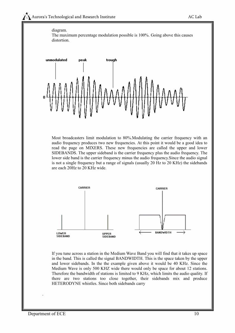
Auroras Technological and Research Institute AC Lab
Department of ECE 11
CIRCUIT DIAGRAMS
AM MODULATION
AM DEMODULATION
CARRIER SIGNAL
TIME T
A
m
p
l i t u
d
e
Ac
Auroras Technological and Research Institute AC Lab
Department of ECE 12
MODULATING SIGNAL
AM MODULATED OUTPUT
AM DEMODULATION OUTPUT
PROCEDURE
A MODULATION i Switch lsquoONrsquo the Trainer Kit
ii Generate the carrier and modulating signal such that carrier frequency must be greater than modulating frequency
iii Apply the carrier and modulating signal into AM modulator input vi Trace the envelope of the modulated waveform
v Repeat step(vi) duly adjusting the modulating signal for under modulation and over modulation
B DEMODULATION
i Apply the modulated AM output into Demodulation input ii Trace the demodulated output waveform
POST- LAB
TIME T
A
m
p
l i t u
d
e
Am
A
m
p
l i t u
d
e
TIME T
Auroras Technological and Research Institute AC Lab
Department of ECE 13
i Observe the frequency and amplitude of the carrier and modulating signal
ii Observe the frequency and maximum peak-peak amplitude(Amax) and minimum peak-
peak amplitude (Amin) of the AM signal in TableI
iii Calculate the modulation index Ч=Amax-AminAmax+Amin
iv Plot the out put waveforms Time T Vs Voltage Vo
v Write result and conclusion
CONCLUSION Hence the AM modulation and demodulation is verified
QUESTIONS 1 what is meant by modulation
2 What is meant by modulation index
3 What is meant by under modulation and over modulation
Auroras Technological and Research Institute AC Lab
Department of ECE 14
EXPERIMENT NO 2
DSB ndash SC Modulator amp Demodulator
OBJECTIVE To study the balanced modulator using IC 1496
PRE-LAB
1 Study the theory of balanced modulator
2 Draw the circuit diagram
3 Draw the expected waveforms
4 Study the datasheet of IC 1496
EQUIPMENT
1 Function generator
2 Dual trace CRO
3 Balanced modulator trainer kit
THEORY
In a balanced modulator a signal is modulated using two carriers that are 180
degrees out of phase The resulting signals are then combined in such a way that the carrier
components cancel leaving a DSB-SC (double sideband suppressed carrier) signal
CIRCUIT DIAGRAM
Auroras Technological and Research Institute AC Lab
Department of ECE 15
BALANCED MODULATOR OUTPUT
Auroras Technological and Research Institute AC Lab
Department of ECE 16
BALANCED DEMODULATOR OUTPUT
PROCEDURE
1 Switch ON the trainer kit
2 Generate the carrier and modulating signal
3 Apply the modulating signal and the carrier signal to the balanced modulator input
4 Observe the balanced modulator output
POST LAB
1 Observe the frequency and amplitude of the carrier and modulating signal
2 Observe the frequency and amplitude of the balanced modulator output
3 Observe the quadrature null effect
4 Plot the output waveforms Time T VS Voltage V
5 Write result and conclusions
CONCLUSIONS The balanced modulator output is verified
QUESTIONS 1 what is the efficiency for DSB SC signal
2 What are the other types of balanced modulators
3 What is meant by pilot carrier
Auroras Technological and Research Institute AC Lab
Department of ECE 17
EXPERIMENT NO 3
SSB ndash SC MODULATOR amp DEMODULATOR
OBJECTIVE To study the Single side band modulation by using Phase shift method and demodulation using synchronous detector method
PRE-LAB
1 Study the theory of SSB
2 Draw the circuit diagram and expected waveforms
EQUIPMENTS 1 Function generator 2
2 Dual trace CRO 1
3 SSB system modulation and demodulation trainer kit 4 Patch CardsConnecting wires
5 Frequency counterMulti meter
THEORY
Single-sideband modulation (SSB) is a refinement of amplitude modulation that more
efficiently uses electrical power and bandwidth It is closely related to vestigial sideband
modulation (VSB)Amplitude modulation produces a modulated output signal that has
twice the bandwidth of the original baseband signal Single-sideband modulation avoids
this bandwidth doubling and the power wasted on a carrier at the cost of somewhat
increased device complexity SSB was also used over long distance telephone lines as part
of a technique known as frequency-division multiplexing (FDM) FDM was pioneered by
telephone companies in the 1930s This enabled many voice channels to be sent down a
single physical circuit for example in L-carrier SSB allowed channels to be spaced
(usually) just 4000 Hz apart while offering a speech bandwidth of nominally 300ndash
3400 Hz Amateur began serious experimentation with SSB after World War II The
Strategic Air Command established SSB as the radio standard for its bombers in 1957[4]
It
has become a de facto standard for long-distance voice radio transmissions since then
Auroras Technological and Research Institute AC Lab
Department of ECE 18
BLOCK DIAGRAM OF SSB MODULATOR
SSB-DEMODULATOR SYSTEM
EXPECTED WAVEFORMS
Auroras Technological and Research Institute AC Lab
Department of ECE 19
DSB-SC 0UTPUT
SSB-SC OUTPUT
PROCEDURE
a Modulation
1 Switch ON the trainer kit 2 Observe the output of RF generator using CROThere are two outputs from the RF
generator one is direct output and another is 90 deg phase shift with the direct output 3 Observe the output of AF generator using CROThere are two outputs from the AF
generator one is direct output and another is 90 deg phase shift with the direct output 4 Set the amplitude of the RF signal to 01vpp and connect the 0 deg phase shift signal to
one BM and 90 deg angle phase shift signal to the second BM
5 Set the AF Signal amplitude to 8vpp and connect to the BM 6 Observe the outputs of both balanced modulators simultaneously and adjust the balance
control until get the output waveforms (DSB SC) 7 To get LSB of SSB connect both balanced modulators outputs to SUBTRACTED circuit 8 Measure the frequencies of LSB using multimeter 9 Calculate the theoretical frequency of the SSB (LSB) and compare it with the practical
value LSB=RE Frequency ndashAF Frequency
10 To get USB of SSB signal connect both balanced modulators outputs to ADDER circuit 11 Measure the frequencies of USB
12 Calculate the theoretical value of the SSB Upper Side Band (SSB-USB) frequency and compare it with practical value
USB=RF Frequency+AF Frequency
Auroras Technological and Research Institute AC Lab
Department of ECE 20
b Demodulation (Synchronous detector)
1 Connect the SSB signal from the summer or sub tractor to the SSB signal input of the synchronous detector and RF signal (0ordm) to the RF input of the synchronous detector
2 Observe the Detector output using CRO and compare it with the AF signal (Modulating Signal)
3 Observe the SSB signal for the different frequencies of the AF signal (modulating signal)
TABULATION RF Frequency (Fc) =--------------------KHz
USB LSB
SNo AFsig
Freq(Fm) Practical Freq Theoretical
Freq=Fc+Fm
Practical Freq
Theoretical Freq=Fc-Fm
POST LAB
1 Observe the frequency and amplitude of the RF carrier both (900 amp 0 0 ) phase AF modulating signal (900 amp 0 0 ) phase DSB-SC SSB-SC LSB and USB of the SSB signal
2 Observe the frequency components and bandwidth of SSB
3 Plot the output waveforms above mentioned 4 Write result and conclusion
CONCLUSIONS Hence various outputs of SSB modulator are obtained
QUESTIONS 1 What are the advantages of SSB over AM
2 What is the main drawback of SSB
3 What is meant by VSB
Auroras Technological and Research Institute AC Lab
Department of ECE 21
EXPERIMENT NO 4
FREQUENCY MODULATION AND DEMODULATION
OBJECTIVE To study
1 Frequency modulation process
2 Measurement of Modulation Index
3 Measurement of Frequency deviation
4 Demodulation Process
PRE-LAB 1 Study the data sheet of IC LM 2206 LM 565
2 Study the theory of FM modulation and demodulation
3 Draw the circuit diagram for modulation and demodulation
4 Draw the expected wave forms
EQUIPMENT 1 Frequency modulation and demodulation trainer kit 1 No 2 Dual trace CRO 1 No 3 Connecting probe and cords
THEORY
In telecommunications frequency modulation (FM) conveys information over a carrier
wave by varying its frequency (contrast this with amplitude modulation in which the amplitude
of the carrier is varied while its frequency remains constant) In analog applications the
instantaneous frequency of the carrier is directly proportional to the instantaneous value of the
input signal Digital data can be sent by shifting the carriers frequency among a set of discrete
values a technique known as keying The instantaneous frequency of the oscillator and is the
frequency deviation which represents the maximum shift away from fc in one direction
assuming xm(t) is limited to the range plusmn1Although it may seem that this limits the frequencies in
use to fc plusmn fΔ this neglects the distinction between instantaneous frequency and spectral
frequency The frequency spectrum of an actual FM signal has components extending out to
infinite frequency although they become negligibly small beyond a point Carsons rule of
thumb Carsons rule states that nearly all (~98) of the power of a frequency-modulated signal
lies within a bandwidth
Auroras Technological and Research Institute AC Lab
Department of ECE 22
CIRCUIT DIAGRAM
MODULATION
DEMODULATION
Auroras Technological and Research Institute AC Lab
Department of ECE 23
OUT PUT WAVEFORMS
Auroras Technological and Research Institute AC Lab
Department of ECE 24
PROCEDURE a Modulation
i Switch ON the trainer kit ii Generate the carrier and modulating signal iii apply the modulating signal to the frequency modulator iv Trace the FM output
b Demodulation i apply the modulated FM output into Demodulation input ii Trace the demodulated output waveform
TABULATION
SNo
Amplitude of Modulating
Signal(Am) Fmin
Frequency
Deviation
∆f=fc-fmin or fc-fmax
Modulation Index β=∆ffm
POST LAB
1 Observe the frequency and amplitude of the carrier and modulating signal 2 Calculate the frequency deviation by observing Fmax and Fmin
δ=Fc-Fmax or δ=Fc-Fmin
3 Calculate modulation index β= δFm
4 Change the amplitude of the modulating signal and repeat steps 1 to 3 for different values of Am and note down the readings in table-1
5 Plot the output waveforms Time T VS Voltage Vo
6 Write result and conclusion
CONCLUSIONS Hence the frequency modulated output is obtained
QUESTIONS 1 what is meant by angle modulation
2 How FM is different from AM
3 What is meant by Carson Rule
4 What is the maximum modulation index
Auroras Technological and Research Institute AC Lab
Department of ECE 25
EXPERIMENT NO 5
STUDY OF SPECTRUM ANALIZER AND ANALYSIS OF AM amp FM SIGNALS
Auroras Technological and Research Institute AC Lab
Department of ECE 26
Auroras Technological and Research Institute AC Lab
Department of ECE 27
Auroras Technological and Research Institute AC Lab
Department of ECE 28
EXPERIMENT NO 6
PRE EMPHASIS AND DE EMPHASIS
OBJECTIVE To study the operation of Pre-emphasis and De-emphasis circuits
PRE-LAB
1 Study the theory of Pre-emphasis and De-emphasis circuits
2 Draw the circuit diagram
3 Draw the expected waveforms
COMPONENTS
1 Resistors 100kΩ 100Ω
2 Capacitors 1μf 100μf EQUIPMENT 1 Function generator 1
2 Dual trace CRO 1
THEORY Pre-emphasis
Improving the signal to noise ratio by increasing the magnitude of higher frequency
signals with respect to lower frequency signals
De-emphasis
Improving the signal to noise ratio by decreasing the magnitude of higher
frequency signals with respect to lower frequency signals
Transmitters that employ a true FM modulator require a pre emphasis circuit before the
modulator fore the true FM modulator doesnt automatically pre emphasize the audio like
a transmitter that uses a phase modulator A separate circuit is not necessary for pre
emphasis in a transmitter that has a phase modulator because the phase modulator applies
pre emphasis to the transmitted audio as a function of the phase modulator The receivers
De emphasis circuitry takes the unnatural sounding pre emphasized audio and turns it
back into its original response Pre emphasized (discriminator) audio is however available
directly from the audio demodulation (discriminator) circuitry In linking systems many
choose to eliminate the emphasis circuitry to allow better representation of retransmitted
Auroras Technological and Research Institute AC Lab
Department of ECE 29
signals Since the signal has already been pre emphasized (by the user that is
transmitting) and since the receiver you are listening to takes care of the de emphasis
CIRCUIT DIAGRAMS
PRE-EMPHASIS
DE-EMPHASIS
EXPECTED WAVEFORMS
INPUT
TIME T
A
m
p
l i t u
d
e
Am
Auroras Technological and Research Institute AC Lab
Department of ECE 30
OUTPUT
PRE-EMPHASIS
Freq Vs Gain
DE-EMPHASIS
Freq Vs Gain
TIME T
Freq f (Hz)
A
m
p
l i t u
d
e
Am
Auroras Technological and Research Institute AC Lab
Department of ECE 31
TABLE
PRE EMPHASIS
SNo Input Freq
Input Voltage Vi (Volts)
Output Voltage Vo (Volts) Gain=VoVi
Gain in dB
20log(voVi)
DE-EMPHASIS
SNo Input Freq
Input Voltage Vi (Volts)
Output Voltage Vo (Volts)
Gain=VoVi Gain in dB
20log(VoVi)
PROCEDURE a Pre-emphasis
1 Connect the circuit as per the circuit diagram
2 Apply a constant sine wave input across the input terminal of fixed amplitude(Vi) 3 By varying the input frequency note down the output amplitude (Vo) with respect to
input frequency in Table 4 Calculate the gain using the formula
5 Gain =20log (Vo) (Vi) db
b De-Emphasis
1 Connect the circuit as per the circuit diagram
2 Repeat the steps 2 3 amp4
POST LAB
1 Observe the output amplitude for both the pre-emphasis and De-emphasis circuits
2 Calculate the gain in db
3 Plot the frequency versus gain curves on logarithmic graphs for both the circuits
4 Plot the input and output waveforms Time T VS Voltage Vo
5 Write the result and conclusion
CONCLUSIONS Obtained the pre emphasis and de-emphasis outputs
QUESTIONS 1 Observe the out put signal is disturbed by noise what action has to be taken and measure the
output voltage 2 Where we use the pre emphasis circuit 3 Where we use the de emphasis circuit 4 What are the advantages of pre emphasis and de emphasis circuits
Auroras Technological and Research Institute AC Lab
Department of ECE 32
EXPERIMENT NO 7
TIME DIVISION MULTIPLEXING AND DEMULTIPLEXING
AIM To study Time Division Multiplexing and its waveforms
PRE LAB WORK
Study the operation of Time division multiplexer and demultiplexer Draw the block diagram of TDM
Draw the expected graphs of all necessary waveforms ( CH1CH2TDM OP and Demultiplexed OP)
EQUIPMENT
1) Experimental board on TDM
2) Dual Trace CRO 3) Probes
THEORY
Time Division Multiplexing (TDM) is a technique for transmitting serial messages on a signal
transmission channel by dividing the time division into slots One slot for each message The concept
of TDM comes from sampling theorem which enables use to transmit the information contained in the
band limited Signal using sampling of the signal taken uniformly or a rate slightly higher then the
Nyquist rate TDM enables the joint utilization at a common transmission channel by a number of
independent message sources without mutual interference
The different Ip message signals all band limited in WHz by the IP low pass filters and sequentially
sampled at the transmitters by a rotary switch or a comparator The switch makes are complete
revolution in Ts frac12 W extracting are sample from each IP The commutator OP is a PAM waveform
containing individual message sample
It there are N number of IP the pulse to Pulse spacing will be Ts = 1 while the spacing
N Nfs
bw successive samples from each IP is called a frame
At the receiver a similar rotatory switch the decommutator separates the samples and distributes them
to a bank of low-pass filters which in turn is usually electronic and synchronization signals are
provided to keep the distribute in step with the commutant
Auroras Technological and Research Institute AC Lab
Department of ECE 33
EXPECTED GRAPHS
PROCUDURE
1 Connect the OP of the experimental board to one of the channels on CRO 2 Switch ON the experimental board 3 Observe the OP waveforms 4 Vary the values of the resistors R1 R2 and R3 alternative and observe the OP on CRO
RESULT
The process of the Time Division Multiplexing and the waveforms has been studied
CONCLUSION
Auroras Technological and Research Institute AC Lab
Department of ECE 34
Figure 1 Time Division Multiplexing amp De multiplexing
Auroras Technological and Research Institute AC Lab
Department of ECE 35
EXPERIMENT NO 9
VERIFICATION OF SAMPLING THEOREM
AIM To study the effect of sampling on the transmission of information through PWM
PRE LAB WORK
Study the sampling theorem
Draw the expected graphs of all necessary waveforms ( message signal carrier wave PWM op demodulated op etc
EQUIPMENT
1) Experimental Board on study of sampling theorem 2) Dual trace CRO (0 ndash 20 MHz) 3) Function Generator 4) Connecting wires
THEORY
The principle of sampling can be explained using the switching sampler The switch periodically shifts below bw two constants at the rate of fs = 1 Ts Hz staying on the IP constant for each sampling period The op Xs(t) of the samples consists of segments of x(t) and Xc(t) can be represented as
Xs(t) = X(t) S(t)
Where S(t) is sampling or switching function There are a number of differences bw the ideal sampling and reconstruction techniques described in the proceeding sections of the actual signal
PROCEDURE
1) Observe the internal clock and measure its frequency and amplitude 2) Give the clock to the clock IP terminal 3) Connect the modulating signal to the IP 4) Check the condition fs gt 2fm and observe the de-modulated wave 5) Check the condition fs lt 2fm and fs = 2fm and draw the OP waveforms
RESULT
CONCLUSION
Aurorarsquos Technological and Research Institute DC Lab
36
Figure 2 Sampling Theorem
Aurorarsquos Technological and Research Institute DC Lab
37
EXPERIMENT NO 10
PULSE AMPLITUDE MODULATION AND DEMODULATION
AIM 1) To study the PAM modulation and its waveforms
2) To study the de-modular of PAM
3) To study the effect of sampling frequency on de-modulation OP
PRE LAB WORK
Study the operation Pulse Amplitude Modulator and Demodulator Draw the block diagram of PAM modulator and demodulator Draw the expected graphs of all necessary waveforms ( message signal carrier wave PAM op
demodulated op etc)
EQUIPMENT
1) Exp Board on study of PAM 2) CRO 3) Functional Generator 4) Connecting wires and chords
THEORY
In PAM the amplitude of the carrier wave of higher frequency follow the amp of the message signal
Within this (Modulation Sampling) we have two more types of sampling those are
(1) Natural Sampling
(2) Flat Top Sampling
Basically in Natural Sampling the carrier waves are train of pulses of a certain frequency After
sampling the top of the Pulse follow the message signal Due to this following of top of Pulses with the
message signals cause a distortion in De-modulation
In Flat top sampling also we use train of pulses for sampling but only the starting point of each pulse
follow the message signal remaining width of the pulse will (follow) be flat But here we go for Natural
sampling
EXPECTED WAVEFORMS
Aurorarsquos Technological and Research Institute DC Lab
38
PROCEDURE (MODULATION)
1 Observe the clock on CRO and measure its frequency and amp (freq 5KHz) 2 Connect the clock to clock IP terminals in modulation 3 Put control switch in ac position and set amplitude = OV This provides DC at Modulating
signal terminal 4 Connect the modulating signal or IP to the modulator 5 Connect one channel of CRO at lsquoTirsquo and Gnd Observe that the pulses are of same height
Height is adjustable by varying offset This is PAM signal with DC IP Measure amplitude and frequency of Pulses
6 Increase the amplitude of modulation signal Observe the amplitude and frequency of this sinusoidal modulating signal
7 Observe PAM signal
a) How many Pulses are there in one modulating cycle
b) It is natural or Flat Top PAM c) It is Single or dual polarity PAM
8 Observe the effect of DC offset on PAM waveform
DE-MODULATION
1) Generate undistorted PAM waveform 2) Connect the modulating signal to de-modulation IP 3) Observe the detected OP and measure its frequency which must be same as
modulating signal
EFFECT OF SAMPLING FREQUENCY
1) Connect internal sinusoidal signal to modulating signal IP of the modulator 2) Connect an external functional Generator at the circuit terminals of the modulator 3) Get the PAM waveform using the above circuit 4) Adjust the modulating amplitude offset and frequency to get an undistorted frequency 5) Connect the PAM to de-modulator IP 6) Observe the demodulated signal for various frequencies of clock (fs gt 2fm lt 2fm = 2 fm)
RESULT
CONCLUSION
Aurorarsquos Technological and Research Institute DC Lab
39
Figure 3 Pulse Amplitude Modulation
Auroras Technological and Research Institute AC Lab
Department of ECE 5
EXPERIMENT NO 11
PULSE WIDTH MODULATION AND DEMODULATION
AIM
1) To study the PWM process and the corresponding waveforms 2) To study the effect of sampling frequency on the transmission of information through PWM
PRE LAB WORK
Study the operation Pulse Width Modulator and Demodulator Draw the block diagram of PWM modulator and demodulator Draw the expected graphs of all necessary waveforms ( message signal carrier wave PWM op
demodulated op etc
EQUIPMENT
1) Experimental Board
2) Dual trace CRO 3) AF generator 4) Multimeter
THEORY
In PWM the samples of the message signal are used to vary the duration of the individual pulses The
pulse width may be varied by varying the time of occurrence of the leading edge trailing edge of both
edges of the pulse in accordance with the sampled value of the modulating wave PWM can also be
generated by using emitter follower monostable multivibrator is an excellent voltage to time converter
since its gate width is dependent on the voltage to which the capacitor is changed If this voltage can be
varied in accordance with a signal voltage a series of rectangular pulses can be obtained with width
varying as required
The demodulated of PWM is quite simple PWM is passed through a low pass filter The reconstruction is
associated with a certain amount of Distortion caused by the cross modulator products that fall in the
signal band
EXPECTED WAVEFORM
Aurorarsquos Technological and Research Institute DC Lab
41
PROCEDURE
STUDY OF MODULATION
1) Observe the clock on CRO and measure its frequency (fs) 2) Observe the sine wave modulating signal on CRO and observe the dc shift produced in this
by varying the offset nob Measure the frequency Variation limits of this signal 3) Apply clock at the circuit input terminal 4) Apply modulating signal by keeping the control switch in dc position 5) Observe the modulated wave 6) Plot the graph bw pulse width and the applied dc voltage 7) Put the control switch in sine wave position and adjust the modulating signal amplitude
frequency and dc offset to get the stationary waveform of PWM 8) Note the number of pulses in one circuit of modulating signal
STUDY OF DEMODULATION
1) Generate the stationary PWM waveform using sin wave modulating signal 2) Connect the modulator OP to PWM demodulator 3) Connect Channel (1) to Modulating Signal and channel (2) to demodulated wave
EFFECT OF SAMPLING FREQUENCY
1) Use an external square wave and connect it to the clock input 2) Set the frequency of square wave at frequency 2fm 3) Observe the demodulated wave
4) Change the frequency of square wave to fs lt 2fm fs gt 2fm and observe the demodulated wave
RESULT
CONCLUSION
Aurorarsquos Technological and Research Institute DC Lab
42
Figure 4 Pulse Width Modulation
Aurorarsquos Technological and Research Institute DC Lab
43
EXPERIMENT NO 12
PULSE POSITION MODULATION AND DEMODULATION
AIM
1) To study the PPM Modulation and the corresponding waveforms 2) To study the de-modulation of PPM 3) To see the effect of sampling frequency on the transmission of information through PPM
PRE LAB WORK
Study the operation Pulse Position Modulator and Demodulator Draw the block diagram of PPM modulator and demodulator Draw the expected graphs of all necessary waveforms ( message signal carrier wave PPM op
demodulated op etc
EQUIPMENT
1) Experimental Board for PPM
2) Dual Phase Oscilloscope
3) AF Generator
THEORY
In PDM long pulses expand considerable power duration If the pulse which bearing no additional
information If this un used power is subtracted from PDM so that only time transitions are preserved
We observe a more efficient type of pulse modulation known as pulse position modulation Here in the
Pulse Position Modulated wave the position of the Pulse relative to its unmodulated time of occurrence is
varied in accordance with the message signal
We generate a PPM wave from PWM wave by using a Monostable Multivibrator The device has one
absolutely stable state and one quest ndash stable state into which it is triggered by an externally applied Pulse
The monostable multivibrator is designed to trigger on the trailing edges of the duration ndash modulated pulse
is varied in accordance with the message signal
The fixed pulse duration of the PPM wave at the monostable multivibrator OP can be set by appropriately
choosing the resistance ndash capacitance combination in the timing circuit of the device
Aurorarsquos Technological and Research Institute DC Lab
44
EXPECTED WAVEFORM
PROCEDURE
STUDY OF MODULATION
Observe the clock and measure its frequency (fs) Apply the clock at the clock IP terminal in the modulator Apply the modulating signal keeping control switch in DC position Observe the PPM OP Connect the channel ndash (1) on CRO to clock and channel (2) to PPM wave OP Compare the position of two waveforms Vary the DC offset and observe the relative shift between the clock and PPM OP Measure the time shift between clock and PPM wave for various settings of offset Draw the graph between time shift and DC voltage Put the control switch in AC position adjusts the amplitude and frequency and offset
of sinusoidal modulating signal to get the stationary PPM wave Note the number of pulses in one cycle of the modulated wave
STUDY OF DEMODULATION
Generate a stationery PPM wave for a sinusoidal modulating signal Apply the PPM wave to the input of de-modulator Connect the Channel ndash (1) of CRO to the modulating signal and channel ndash 2 to the
de-modulator output Compare the two waveforms
Note the frequency of demodulated wave It should be same as the modulating signal Note down the waveform
RESULT
CONCLUSION
Aurorarsquos Technological and Research Institute DC Lab
45
Aurorarsquos Technological and Research Institute DC Lab
46
Figure 5 Pulse Position Modulation
Aurorarsquos Technological and Research Institute AC Lab
47
EXPERIMENT NO 13
FREQUENCY SYNTHESIZER
AIM
To study the operation of frequency synthesizer using PLL
PRE-LAB 1 Study the data sheet of IC 7404IC 4017IC 565 and IC 4046
2 Study the theory of frequency synthesizer 3 Draw the circuit diagram and expected waveforms
EQUIPMENTS
1 Frequency synthesizer trainer AET -26A
2 Dual trace CRO (20Mhz) 3 Digital frequency counter or multimeter
4 Patch chords
THEORY
A frequency synthesizer is an electronic system for generating any of a range
of frequencies from a single fixed time base or oscillator They are found in many modern
devices including radio receivers mobile telephones radiotelephones walkie-talkies CB
radios satellite receivers GPS systems etc A frequency synthesizer can combine
frequency multiplication frequency division and frequency mixing (the frequency mixing
process generates sum and difference frequencies) operations to produce the desired output
signal
BLOCK DIAGRAM
Phase Comparator
Amplifier Low pass filter
V C O
Div N Network frequency divider
Fin= fout
N
fin
Fout =Nf in
Aurorarsquos Technological and Research Institute AC Lab
48
SIMPLE 1KHZ-9KHZ FREQUENCY SYNTHESIZER
CIRCUIT DAIGRAM
PROCEDURE 1 Switch on the trainer ad verify the output of the regulated power supply ie 5V These
supplied are internally connected to the circuit so no extra connections are required 2 Observe output of the square wave generator using oscilloscope and measure the range
with the help of frequency counter frequency range should be around 1KHz to 10KHz 3 Calculate the free running frequency range of the circuit (VCO output between 4th pin
and ground 1 For different values of timing resistor R1 ( to measure Rt value using digital multimeter between given test points 1 And record the frequency values in table 1
Fout = 03 (RtCt) where Rt is the timing resistor and Ct is the timing capacitor = 001 f
Aurorarsquos Technological and Research Institute AC Lab
49
4 Connect 4th pin of LM 565 (Fout) to the driver stage and 5th pin (Phase comparator) connected to 11th pin of 7404 Output can be taken at the 11th pin of the 7490 It should be divided by the 2 amp 3 times of the fout
TABULATION
Fin KHz Fout = N x fin KHz Divided by 3 2
EXPECTED WAVEFORMS
POST LAB
1 Observe the synthesized output in table 2 Calculate the output frequency
3 Plot the output waveforms
4 Write result and conclusions
CONCLUSIONS
The various outputs of frequency synthesizer are verified
QUESTIONS
1 What are the applications of frequency synthesizer
TIME T
A
m
p
l i T
u
d
e
Ac
Aurorarsquos Technological and Research Institute AC Lab
50
2 What is the difference between heterodyning and synthesizer
Aurorarsquos Technological and Research Institute AC Lab
51
EXPERIMENT NO 14
AGC CHARATERISTICS
AIM
To observe the effect of automatic gain control(AGC)
PRE LAB 1 To study the theory of AGC 2 Draw the Block Diagram circuits diagram and expected waveforms
EQUIPMENTS 1 AGC Trainer Kit 2 CRO
3 Patch Chords
4 Digital Multimeter
THEORY
Automatic gain control (AGC) is an adaptive system found in many electronic
devices The average output signal level is fed back to adjust the gain to an appropriate level
for a range of input signal levels For example without AGC the sound emitted from an AM
radio receiver would vary to an extreme extent from a weak to a strong signal the AGC
effectively reduces the volume if the signal is strong and raises it when it is weaker AGC
algorithms often use a PID controller where the P term is driven by the error between
expected and actual output amplitude
Block Diagram
Frequency Converter
1st IF Amplifier
2nd IF Amplifier
Detector
Audio Preamplifier
Driver Output
Aurorarsquos Technological and Research Institute AC Lab
52
CIRCUIT DIAGRAM
PROCEDURE
1 Connect 455 KHz IF Signal Function Generator connect AGC link Connect CRO channel-1 at input terminals
2 Connect CRO channel 2 at collector of Q3 The amplified signal will be observed 3 Calculate the voltage gain by measuring the amplitude of output signal (Vo) waveform
using formula A=VoVi 4 Now connect CRO-2 channel at output The detected audio signal of 455 Khz will be
observed 5 Now vary input level of 455 KHz IF signal and observe detected 455 KHz audio signal
with and without AGC link The output will be distorted when AGC link is removed ie there is no AGC action
6 This explains AGC effect in Radio circuit
TABULATION
SNo Input Voltage Vi (P-P) With out AGC With AGC
Output Voltage Vo (P-P)
Gain A= Vo Vi
Output Voltage Vrsquoo (P-P)
Gain Arsquo= Vrsquoo Vi
Aurorarsquos Technological and Research Institute AC Lab
53
EXPECTED WAVEFORMS
AM Modulated RF Input
Detected Output with AGC
Detected Output without AGC
POST-LAB
1 Observe the input voltage and output voltage for with AGC and Without AGC in Table 1
2 Calculate Gain a=vovi for both cases 3 Plot the output waveforms Time T Vs Voltage Vo and input voltage Vi Vs Gain A 4 Write Result and Conclusions
CONCLUSIONS The AGC characteristics are verified
QUESTIONS 1 what is meant by AGC
2 What is the difference between simple AGC and delayed AGC
3 From which part of receiver AGC is obtained
TIME T
A
m
p
l i T
u
d
e
Ac
TIME T
A
m
p
l i T
u
d
e
Ac
TIME T
A
m
p
l i T
u
d
e
Ac
Aurorarsquos Technological and Research Institute AC Lab
54
EXPERIMENT NO 15
PHASE LOCKED LOOP
OBJECTIVE To study the Phase locked loop using 565 IC and to take input frequency given by an external signal source
PRE-LAB To Study
1 The data sheet of IC 565
2 The theory of Phase locked loop
3 About free running frequency locking range and capture range
4 Draw the circuit diagram and expected waveforms
EQUIPMENT 1 Function generator 2
2 Dual trace CRO 1
3 Phase locked loop trainer kit
THEORY
A phase-locked loop or phase lock loop (PLL) is a control system that generates a signal
that has a fixed relation to the phase of a reference signal A phase-locked loop circuit
responds to both the frequency and the phase of the input signals automatically raising or
lowering the frequency of a controlled oscillator until it is matched to the reference in both
frequency and phase A phase-locked loop is an example of a control system using negative
feedback Phase-locked loops are widely used in radio telecommunications computers and
other electronic applications They may generate stable frequencies recover a signal from a
noisy communication channel or distribute clock timing pulses in digital logic designs
such as microprocessors Since a single integrated circuit can provide a complete phase-
locked-loop building block the technique is widely used in modern electronic devices
with output frequencies from a fraction of a cycle per second up to many gigahertz
BLOCK DIAGRAM
Aurorarsquos Technological and Research Institute AC Lab
55
CIRCUIT DIAGRAM
PROCEDURE 1 Switch ON the trainer kit 2 Check the VCO output at pin 4 of IC 565 that is a square wave form The frequency of the
VCO Output depends on CT (001f) and RT (47kΩ) 3 Next short the pins 4amp5 and give signal of variable frequency and observe VCO output 4 Change the input frequency and observe the VCO output on the CRO 5 Between some frequencies the VCO output is locked to the input signal frequency This can
be observed by increasing or decreasing the frequency of the VCO output by changing input frequency
6 Before or after that frequency range the VCO output is not locked
7 Calculate Lock range (FL) and capture range (FC) by using the following formulas
FL = 8foVCO fo=03RtCT
FC=12π radic2πf236103 C2
Table1
SNo Locking Frequency Frequency Range From To
CHARTERISTICES
Aurorarsquos Technological and Research Institute AC Lab
56
CONCLUSIONS Obtained the lock range of PLL
QUESTIONS
1 Observe the VCO output when pins 4amp5 short and give square wave as signal 2 Define lock range and capture range
3 What are the basic applications of PLL
Aurorarsquos Technological and Research Institute AC Lab
57
ANNEXURE-I
EXPERIMENT NO 1
Aurorarsquos Technological and Research Institute AC Lab
58
CHARACTERISTICS OF MIXER
AIM
To study the functioning of a frequency mixer
PRE LAB 1 To study the theory of Mixer 2 Draw the circuit diagram and expected waveforms
EQUIPMENTS 1 Frequency mixer trainer kit 2 CRO (20MHz) 3 Connecting cords and probes 4 Function generator (1MHz)
THEORY
In receivers using the super heterodyne principle a signal at variable frequency is
converted to a fixed lower frequency IF before detection IF is called the intermediate frequency
In typical AM (Amplitude Modulation eg as used on medium wave) home receivers that
frequency is usually 455 kHz for FM VHF receivers it is usually 107 MHz An intermediate
frequency (IF) is a frequency to which a carrier frequency is shifted as an intermediate step in
transmission or reception Frequency modulation (FM) is a form of modulation that represents
information as variations in the instantaneous frequency of a carrier wave Very high frequency
(VHF) is the radio frequency range from 30 MHz (wavelength 10 m) to 300 MHz (wavelength 1
heterodyne receivers mix all of the incoming signals with an internally generated waveform
called the local oscillator The user tunes the radio by adjusting the sets oscillator frequency in
the mixer stage of a receiver the local oscillator signal multiplies with the incoming signals
which shifts them all down in frequency The one that shifts is passed on by tuned circuits
amplified and then demodulated to recover the original audio signal The oscillator also shifts a
copy of each incoming signal up in frequency by amount Those very high frequency images
are all rejected by the tuned circuits in the IF stage The Super heterodyne receiver (or to give it its
full name The Supersonic Heterodyne Receiver usually these days shortened to superhet) was
invented by Edwin Armstrong in 1918
Aurorarsquos Technological and Research Institute AC Lab
59
BLOCK DIAGRAM
CIRCUIT DIAGRAM
EXPECTED WAVEFORMS
INPUT SIGNAL Fx
INPUT SIGNAL Fy
TIME T
A
m
p
l i T
u
d
e
Ac
Aurorarsquos Technological and Research Institute AC Lab
60
MIXER OUTPUT(Fy-Fx)
PROCEDURE 1 Connect the circuit as per the given circuit diagram 2 Switch on the power supply of trainer kit 3 Apply a sine wave at input Fx of 2 VP-P amplitude and 100 KHz frequency 4 Apply a sine wave at input FY of 2 VP-P amplitude and 100 KHz frequency 5 Observe the output waveform on the CRO 6 Repeat the steps 34 and 5 by changing the values of Fx once greater than and less than
FY in a steps of 5Khz (in the range 80KHz to 120KHz)
TABULATION
TIME T
A
M
P
L
I T
U
D
E
TIME T
A
m
p
l i T
u
d
e
Ac
Aurorarsquos Technological and Research Institute AC Lab
61
SNo Freq (Fy)
(kHz) Amp(V) Freq(Fx) (kHz) Amp(V) Freq(Fy-Fx)
(kHz) Amp(V)
POST LAB 1 Observe the amplitude and time Of inputs and output in table
2 Draw the expected waveforms
3 Verify the output signal obtained with the theoretical value 4 Plot the graphs for Time T VS input signal (FX) Voltage V input signal (FY) Voltage V
and output Signal F(x-y) voltage V 5 Write result and conclusions
CONCLUSIONS
Obtained the output of the mixer for various inputs
QUESTIONS
1 what are the different types of mixtures available
2 What is meant by heterodyning
3 What is meant by IF
Aurorarsquos Technological and Research Institute AC Lab
62
EXPERIMENT NO 2
DIGITAL PHASE DETECTOR
OBJECTIVE To detect the phase difference between two square wave signals using digital phase detector
PRE LAB
1 To study the theory of digital phase detector and EX-OR gate operation and truth table 2 Draw the circuit diagram and expected output and input waveforms
EQUIPMENT 1 Digital phase detector trainer kit 2 Regulated power supplies
3 CRO (20MHz) 4 Connecting cords amp probes
5 Digital frequency counter or multimeter
THEORY
Phase detector is a frequency mixer or analog multiplier circuit that generates a voltage
signal which represents the difference in phase between two signal inputs It is an essential
element of the phase-locked loop (PLL)Detecting phase differences is very important in many
applications such as motor control radar and telecommunication systems servo mechanisms and
demodulators
Electronic phase detector
Some signal processing techniques such as those used in radar may require both the amplitude
and the phase of a signal to recover all the information encoded in that signal One technique is to
feed an amplitude-limited signal into one port of a product detector and a reference signal into the
other port the output of the detector will represent the phase difference between the signals If the
signal is different in frequency from the reference the detector output will be periodic at the
difference frequency Phase detectors for phase-locked loop circuits may be classified in two
types A Type I detector is designed to be driven by analog signals or square-wave digital signals
and produces an output pulse at the difference frequency The Type I detector always produces an
output waveform which must be filtered to control the phase-locked loop variable frequency
oscillator (VCO) A type II detector is sensitive only to the relative timing of the edges of the input
and reference pulses and produces a constant output proportional to phase difference when both
signals are at the same frequency This output will tend not to produce ripple in the control voltage
of the VCO
Aurorarsquos Technological and Research Institute AC Lab
63
BLOCK DIAGRAM OF PLL
CIRCUIT DIAGRAM
Aurorarsquos Technological and Research Institute AC Lab
64
EXPECTED WAVEFORMS
EX-OR PHASE DETECTOR
EDGE TRIGGERED OUTPUT
PROCEDURE
1 Switch on the trainer kit
2 Observe the output of the square wave generator available on the trainer kit using CRO
and measure the range with the help of frequency counter the frequency range should be
around 2 KHz to 13 KHz
3 Calculate the free running range of the VCO output ie between 4th pin of IC PLL 565
and ground For different values of timing resistor Rt fout is given by Fout =03 Rt Ct
where Ct timing capacitor = 001 μF Rt timing resistor
4 Connect the square wave to the input of IC PLL 565 and short 4th and 5th pin of PLL
Vary the input frequency of the square wave when the PLL is locked that is connected to
Aurorarsquos Technological and Research Institute AC Lab
65
one input fout EX-OR phase detector The other input fin of EX-OR phase detector is the
coming from inbuilt of square wave generator
5 Connect the pulse generator output to the input of IC 565 PLL and short 4th amp 5th pin of
PLL Vary the input frequency of the square wave when the PLL is locked that is
connected to one input of Edge triggered phase detector input ie fout The other input fin
of edge triggered phase detector is the pulse input coming from the inbuilt pulse generator
6 The dc output voltage of the exclusive-OR phase detector is a function of the phase
difference between its two inputs fin and fout
POST LAB
1 Observe the Voltage and Time of the two input square waves
2 Observe difference of two inputs as square wave output
3 Plot the inputs and output waveforms Time T VS Voltage V
CONCLUSIONS
The phase detector outputs are verified
QUESTIONS
1 What is the function of phase detector
2 What is the condition for getting maximum output
3 Advantages of digital phase detector over analog phase detector
Aurorarsquos Technological and Research Institute AC Lab
66
EXPERIMENT NO 3
COASTAS RECEIVER
AIM
To demodulate a DSB-SC signal using coastas receiver
PRE LAB 1 To study the operation of coastas receiver 2 Draw the circuit diagram and expected waveforms
EQUIPMENTS 1 Communications trainer kit 2 DSB-SC modulator trainer kit 3 CRO (20MHz) 4 Connecting cords and probes 5 Function generator (1MHz)
THEORY
This loop and its variations is much-used as a method of carrier acquisition (and
simultaneous message demodulation) in communication systems both analog and digital
It has the property of being able to derive a carrier from the received signal even when there is
no component at carrier frequency present in that signal (eg DSBSC) The requirement is that
the amplitude spectrum of the received signal be symmetrical about this frequency
The Costas loop is based on a pair of quadrature modulators - two multipliers
fed with carriers in phase-quadrature These multipliers are in the in-phase (I) and quadrature
phase (Q) arms of the arrangement Each of these multipliers is part of separate synchronous
demodulators The outputs of the modulators after filtering are multiplied together in a third
multiplier and the lowpass components in this product are used to adjust the phase of the local
carrier source - a VCO - with respect to the received signal The operation is such as to
maximise the output of the I arm and minimize that from the Q arm The output of the I arm
happens to be the message and so the Costas loop not only acquires the carrier but is a
(synchronous) demodulator as well A complete analysis of this loop is non-trivial It would
include the determination of conditions for stability and parameters such as lock range capture
range and so on
Aurorarsquos Technological and Research Institute AC Lab
67
BLOCK DIAGRAM
EXPECTED WAVEFORMS
DSB-SC modulated output
Aurorarsquos Technological and Research Institute AC Lab
68
Demodulated output of the coastas loop
PROCEDURE
1 Switch ON the DSB-SC trainer kit
2 Generate the carrier and modulating signal
3 Generate the DSB-SC modulated signal
4 Connect the required blocks of the coastas receiver in the communications kit
5 Apply the generated DSB-SC signal to the above connected coastas receiver
6 Observe that the output of the coastas receiver is the demodulated wave of DSB-SC signal
POST LAB
1 Observe the frequency and amplitude of the carrier and modulating signal
2 Observe the frequency and amplitude of the balanced modulator output
3 Observe the lock condition of the coastas loop
4 observe the output of the coastas demodulator
5 Write result and conclusions
CONCLUSIONS The balanced modulator output and the operation of coastas receiver is verified
QUESTIONS 1 what is the operation of coastas loop
2 What happens when the locking condition of the coastas loop occurs
3 Coastas loop can be used for demodulation of other modulation techniques also What are they
Aurorarsquos Technological and Research Institute AC Lab
69
MATLAB PROGRAMMES
Aurorarsquos Technological and Research Institute AC Lab
70
INDEX
1 Introduction - 70
2 Amplitude Modulation and Demodulation - 74
3 DSB-SC Modulation and Demodulation - 84
4 SSB-SC Modulation and Demodulation - 89
5 Frequency Modulation and Demodulation - 95
6 Phase Modulation and Demodulation - 99
7 Time Division Multiplexing and Demultiplexing - 100
8 Frequency Division Multiplexing and Demultiplexing- 103
9 Verification of Sampling Theorem - 104
10 Pulse Amplitude Modulation and Demodulation - 106
11 Pulse width Modulation and Demodulation - 108
12 Pulse Position Modulation and Demodulation - 110
13 PLL as FM Demodulator - 112
Aurorarsquos Technological and Research Institute AC Lab
71
1 INTRODUCTION
What Is Simulink
Simulink is a software package for modeling simulating and analyzing dynamic
systems It supports linear and nonlinear systems modeled in continuous time sampled time
or a hybrid of the two Systems can also be multirate ie have different parts that are
sampled or updated at different rates
Tool for Simulation
Simulink encourages you to try things out You can easily build models from scratch
or take an existing model and add to it You have instant access to all the analysis tools in
MATLABreg so you can take the results and analyze and visualize them A goal of Simulink
is to give you a sense of the fun of modeling and simulation through an environment that
encourages you to pose a question model it and see what happens
Simulink is also practical With thousands of engineers around the world using it to
model and solve real problems knowledge of this tool will serve you well throughout your
professional career
Tool for Model-Based Design
With Simulink you can move beyond idealized linear models to explore more realistic
nonlinear models factoring in friction air resistance gear slippage hard stops and the other
things that describe real-world phenomena Simulink turns your computer into a lab for
modeling and analyzing systems that simply wouldnt be possible or practical otherwise
whether the behavior of an automotive clutch system the flutter of an airplane wing the
dynamics of a predator-prey model or the effect of the monetary supply on the economy
For modeling Simulink provides a graphical user interface (GUI) for building models
as block diagrams using click-and-drag mouse operations With this interface you can draw
the models just as you would with pencil and paper (or as most textbooks depict them) This
is a far cry from previous simulation packages that require you to formulate differential
equations and difference equations in a language or program Simulink includes a
comprehensive block library of sinks sources linear and nonlinear components and
connectors You can also customize and create your own blocks For information on creating
your own blocks see the separate Writing S-Functions guide
Models are hierarchical so you can build models using both top-down and bottom-up
approaches You can view the system at a high level then double-click blocks to go down
through the levels to see increasing levels of model detail This approach provides insight into
how a model is organized and how its parts interact
After you define a model you can simulate it using a choice of integration methods either
from the Simulink menus or by entering commands in the MATLAB Command Window The
menus are particularly convenient for interactive work while the command-line approach is
very useful for running a batch of simulations (for example if you are doing Monte Carlo
simulations or want to sweep a parameter across a range of values) Using scopes and other
display blocks you can see the simulation results while the simulation is running In addition
Aurorarsquos Technological and Research Institute AC Lab
72
you can change many parameters and see what happens for what if exploration The
simulation results can be put in the MATLAB workspace for post processing and
visualization
Model analysis tools include linearization and trimming tools which can be accessed
from the MATLAB command line plus the many tools in MATLAB and its application
toolboxes And because MATLAB and Simulink are integrated you can simulate analyze
and revise your models in either environment at any point
1 Generation of cosine wave in time domain and frequency
domain Clc clear all close all x = -500015 t = 0140001 time = cos(23141000t) y1 = cos(23141000x) subplot(211) plot(xy1) axis([-5 5 -3 3]) grid on title(Time domain) xlabel(Time ) ylabel(Amplitude) now create a frequency vector for the x-axis and plot the magnitude and phase subplot(212) fre = abs(fft(time)) f = (0length(fre) - 1)4000length(fre) plot(ffre) grid on title(Frequency domain (Spectrum)) xlabel(Freq ) ylabel(Amplitude)
WAVEFORMS
Aurorarsquos Technological and Research Institute AC Lab
73
2 Generation of square wave in time domain and frequency
domain
clc clear all close all x = -500015 Fs = 399 t = 01Fs1 time = SQUARE(2pi1000t) y1 = SQUARE(23141000x) subplot(211) plot(xy1) axis([-5 5 -3 3]) grid on xlabel(Time domain) ylabel(Amplitude) now create a frequency vector for the x-axis and plot the magnitude and phase subplot(212) fre = abs(fft(time)) f = (0length(fre) - 1)Fslength(fre) plot(ffre) grid on xlabel(Freq domain) ylabel(Amplitude)
WAVEFORMS
Aurorarsquos Technological and Research Institute AC Lab
74
Aurorarsquos Technological and Research Institute AC Lab
75
2 AMPLITUDE MODULATION AND DEMODULATION PROGRAM 1
clc clear all close all Ac=1 Carrier Amplitude Fc=04 Carrier frequency Fm=005 baseband frequency Fs=10 sampling t=001200 mt=cos(2piFmt) under modulation mu=05 st=Ac(1+mumt)cos(2piFct) subplot(211) plot(tst) hold on plot(tAc(mumt+ones(1length(mt)))r) plot(t-Ac(mumt+ones(1length(mt)))r) hold off title(Modulation Index = 05 under modulation Ac(1+05cos(2pi005t))cos(2pi04t)) xlabel(time (s))ylabel(amplitude) st_fft=fft(st) st_fft=fftshift(st_fft) st_fft_fre=5linspace(-11length(st_fft)) subplot(212) plot(st_fft_freabs(st_fft)) title(spectrum with Modulation Index = 05) xlabel(Frequency (Hz))axis([-1 1 0 1000Ac+100])
total modulation figure mu=1 st=Ac(1+mumt)cos(2piFct) subplot(211) plot(tst) hold on plot(tAc(mumt+ones(1length(mt)))r) plot(t-Ac(mumt+ones(1length(mt)))r) hold off title(Modulation Index = 1 modulation Ac(1+1cos(2pi005t))cos(2pi04t)) xlabel(time (s))ylabel(amplitude) st_fft=fft(st) st_fft=fftshift(st_fft) st_fft_fre=Fs2linspace(-11length(st_fft)) subplot(212) plot(st_fft_freabs(st_fft)) title(spectrum with Modulation Index = 1) xlabel(Frequency (Hz))axis([-1 1 0 1000Ac+100])
Aurorarsquos Technological and Research Institute AC Lab
76
over Modulation figure mu=2 st=Ac(1+mumt)cos(2piFct) subplot(211) plot(tst) hold on plot(tAc(mumt+ones(1length(mt)))r) plot(t-Ac(mumt+ones(1length(mt)))r) hold offtitle(Modulation Index = 2 over modulation Ac(1+2cos(2pi005t))cos(2pi04t)) xlabel(time (s))ylabel(amplitude) st_fft=fft(st) st_fft=fftshift(st_fft) st_fft_fre=Fs2linspace(-11length(st_fft)) subplot(212) plot(st_fft_freabs(st_fft)) title(spectrum with Modulation Index = 2) xlabel(Frequency (Hz))axis([-1 1 0 1000Ac+100])
WAVEFORMS
Aurorarsquos Technological and Research Institute AC Lab
77
PROGRAM 2
Aurorarsquos Technological and Research Institute AC Lab
78
task 1 fc=154000
task 2 fm=fc10 fs=100fc t=01fs4fm xc=cos(2pifct) xm=cos(2pifmt) figure(1) subplot(211)plot(txc) title(carrier signal of 154 khz) xlabel(time (sec)) ylabel(amplitude) subplot(212)plot(txm) title(message signal of 154 khz) xlabel(time (sec)) ylabel(amplitude) DSB-SC MODULATION mu = input( enter the Modulation Index value ) z1=(1+muxm)xc figure(2)
task 31 subplot(211)plot(tz1) title(AMPLITUDE MODULATION IN TIME DAOMAIN) xlabel(time (sec)) ylabel(amplitude)
task 32 l1=length(z1) f=linspace(-fs2fs2l1) Z1=fftshift(fft(z1l1)l1) subplot(212)plot(fabs(Z1)) title(AMPLITUDE MODULATION IN FREQUENCY DOMAIN) xlabel(frequency(hz)) ylabel(amplitude) axis([-200000 200000 0 03])
task 33 demodulation s1=z1xc S1=fftshift(fft(s1length(s1))length(s1)) figure(3) plot(fabs(S1)) title( demodulated signal IN FREQUENCY DOMAIN before filtring) xlabel(frequency(hz)) ylabel(amplitude) axis([-200000 200000 0 03]) hold on Hlp=1sqrt(1+(ffc)^(2100)) plot(fHlpr) title( frequency response of low pass filter) xlabel(frequency(hz)) ylabel(amplitude) axis([-200000 200000 0 2])
task 34 E1=HlpS1 figure(4) subplot(211)plot(fE1)
Aurorarsquos Technological and Research Institute AC Lab
79
title( Recover signal IN FREQUENCY DOMAIN after filtring) xlabel(frequency(hz)) ylabel(amplitude) axis([-200000 200000 0 03]) e1=ifft(ifftshift(E1))length(E1) subplot(212)plot(t(105)e1) title( Recover signal IN Time DOMAIN after filtring) xlabel(time(sec)) ylabel(amplitude)
WAVEFORMS
enter the Modulation Index value 05
0 1 2 3
x 10-4
-1
-05
0
05
1carrier signal of 154 khz
time (sec)
am
plit
ude
0 1 2 3
x 10-4
-1
-05
0
05
1message signal of 154 khz
time (sec)
am
plit
ude
Aurorarsquos Technological and Research Institute AC Lab
80
0 1 2 3
x 10-4
-2
-1
0
1
2AMPLITUDE MODULATION IN TIME DAOMAIN
time (sec)
am
plit
ude
-2 -15 -1 -05 0 05 1 15 2
x 105
0
01
02
AMPLITUDE MODULATION IN FREQUENCY DOMAIN
frequency(hz)
am
plit
ude
-2 -15 -1 -05 0 05 1 15 2
x 105
0
02
04
06
08
1
12
14
16
18
2 frequency response of low pass filter
frequency(hz)
am
plit
ude
Aurorarsquos Technological and Research Institute AC Lab
81
enter the Modulation Index value 1
-2 -15 -1 -05 0 05 1 15 2
x 105
0
01
02
Recover signal IN FREQUENCY DOMAIN after filtring
frequency(hz)
am
plit
ude
0 1 2 3
x 10-4
05
1
15
2 Recover signal IN Time DOMAIN after filtring
time(sec)
am
plit
ude
0 1 2 3
x 10-4
-2
-1
0
1
2AMPLITUDE MODULATION IN TIME DAOMAIN
time (sec)
am
plit
ude
-2 -15 -1 -05 0 05 1 15 2
x 105
0
01
02
AMPLITUDE MODULATION IN FREQUENCY DOMAIN
frequency(hz)
am
plit
ude
Aurorarsquos Technological and Research Institute AC Lab
82
enter the Modulation Index value 2
-2 -15 -1 -05 0 05 1 15 2
x 105
0
02
04
06
08
1
12
14
16
18
2 frequency response of low pass filter
frequency(hz)
am
plit
ude
-2 -15 -1 -05 0 05 1 15 2
x 105
0
01
02
Recover signal IN FREQUENCY DOMAIN after filtring
frequency(hz)
am
plit
ude
0 1 2 3
x 10-4
0
1
2
3 Recover signal IN Time DOMAIN after filtring
time(sec)
am
plit
ude
Aurorarsquos Technological and Research Institute AC Lab
83
0 1 2 3
x 10-4
-4
-2
0
2
4AMPLITUDE MODULATION IN TIME DAOMAIN
time (sec)
am
plit
ude
-2 -15 -1 -05 0 05 1 15 2
x 105
0
01
02
AMPLITUDE MODULATION IN FREQUENCY DOMAIN
frequency(hz)
am
plit
ude
-2 -15 -1 -05 0 05 1 15 2
x 105
0
02
04
06
08
1
12
14
16
18
2 frequency response of low pass filter
frequency(hz)
am
plit
ude
Aurorarsquos Technological and Research Institute AC Lab
84
-2 -15 -1 -05 0 05 1 15 2
x 105
0
01
02
Recover signal IN FREQUENCY DOMAIN after filtring
frequency(hz)
am
plit
ude
0 1 2 3
x 10-4
-2
0
2
4 Recover signal IN Time DOMAIN after filtring
time(sec)
am
plit
ude
Aurorarsquos Technological and Research Institute AC Lab
85
3 DOUBLE SIDEBAND ndash SUPRESSED CARRIER MODULATION
AND DEMODULATION
PROGRAM 1 clc clear all close all Ts = 199 subplot(411) t = 01Ts1 m = cos(2pi1000t) plot(tm) title(Modulating Signal ) xlabel(Time) ylabel(Amplitude) grid on plot of the carrier signal
subplot(412) c = cos(2pi5000t) plot(tc) title(Carrier Signal ) xlabel(Time) ylabel(Amplitude) grid on plot of the DSB signal with Suppresed carrier intime domain
subplot(413) d = mc plot(td) title(DOUBLE SIDEBAND ndash SUPRESSED CARRIER SIGNAL ) xlabel(Time) ylabel(Amplitude) grid on freq domain of the DSB signal
subplot(414) fre = abs(fft(d)) f = (0length(fre) - 1)Tslength(fre) plot(ffre) axis([0 100 0 50]) grid on title(DOUBLE SIDEBAND ndash SUPRESSED CARRIER SPECTRUM ) xlabel(Freq domain) ylabel(Amplitude)
Aurorarsquos Technological and Research Institute AC Lab
86
WAVEFORMS
0 01 02 03 04 05 06 07 08 09 1-1
0
1Modulating Signal
Time
Am
plit
ude
0 01 02 03 04 05 06 07 08 09 1-1
0
1Carrier Signal
Time
Am
plit
ude
0 01 02 03 04 05 06 07 08 09 1-1
0
1DOUBLE SIDEBAND ndash SUPRESSED CARRIER SIGNAL
Time
Am
plit
ude
0 10 20 30 40 50 60 70 80 90 1000
50DOUBLE SIDEBAND ndash SUPRESSED CARRIER SPECTRUM
Freq domain
Am
plit
ude
Aurorarsquos Technological and Research Institute AC Lab
87
PROGRAM 2 task 1 fc=154000 task 2 fm=fc10 fs=100fc t=01fs4fm xc=cos(2pifct) xm=cos(2pifmt) figure(1) subplot(211)plot(txc) title(carrier signal of 154 khz) xlabel(time (sec)) ylabel(amplitude) subplot(212)plot(txm) title(message signal of 154 khz) xlabel(time (sec)) ylabel(amplitude) DSB-SC MODULATION z1= xmxc figure(2) task 31 subplot(211)plot(tz1) title(DSB-SC MODULATION IN TIME DAOMAIN) xlabel(time (sec)) ylabel(amplitude) task 32 l1=length(z1) f=linspace(-fs2fs2l1) Z1=fftshift(fft(z1l1)l1) subplot(212)plot(fabs(Z1)) title(DSB SC MODULATION IN FREQUENCY DOMAIN) xlabel(frequency(hz)) ylabel(amplitude) axis([-200000 200000 0 03]) task 33 demodulation s1=z1xc S1=fftshift(fft(s1length(s1))length(s1)) figure(3) plot(fabs(S1)) title( demodulated signal IN FREQUENCY DOMAIN before filtring) xlabel(frequency(hz)) ylabel(amplitude) axis([-200000 200000 0 03]) hold on Hlp=1sqrt(1+(ffc)^(2100)) plot(fHlpg) title( frequency response of low pass filter) xlabel(frequency(hz)) ylabel(amplitude) axis([-200000 200000 0 2]) task 34 E1=HlpS1 figure(4) subplot(211)plot(fE1) title( Recover signal IN FREQUENCY DOMAIN after filtring) xlabel(frequency(hz)) ylabel(amplitude) axis([-200000 200000 0 03]) e1=ifft(ifftshift(E1))length(E1) subplot(212)plot(t(105)e1)
Aurorarsquos Technological and Research Institute AC Lab
88
title( Recover signal IN Time DOMAIN after filtring) xlabel(time(sec)) ylabel(amplitude) WAVEFORMS
0 1 2 3
x 10-4
-1
-05
0
05
1carrier signal of 154 khz
time (sec)
ampl
itude
0 1 2 3
x 10-4
-1
-05
0
05
1message signal of 154 khz
time (sec)
ampl
itude
0 1 2 3
x 10-4
-1
-05
0
05
1DSB-SC MODULATION IN TIME DAOMAIN
time (sec)
ampl
itude
-2 -15 -1 -05 0 05 1 15 2
x 105
0
01
02
DSB SC MODULATION IN FREQUENCY DOMAIN
frequency(hz)
ampl
itude
Aurorarsquos Technological and Research Institute AC Lab
89
-2 -15 -1 -05 0 05 1 15 2
x 105
0
02
04
06
08
1
12
14
16
18
2 frequency response of low pass filter
frequency(hz)
ampl
itude
-2 -15 -1 -05 0 05 1 15 2
x 105
0
01
02
Recover signal IN FREQUENCY DOMAIN after filtring
frequency(hz)
am
plit
ude
0 1 2 3
x 10-4
-1
0
1
2 Recover signal IN Time DOMAIN after filtring
time(sec)
am
plit
ude
Aurorarsquos Technological and Research Institute AC Lab
90
4 SINGLE SIDE BAND - SUPRESSED CARRIER MODULATION AND DEMODULATION
PROGRAM 1
clc clear all close all Ts = 199 subplot(411) t = 01Ts1 xm = cos(2pi1000t) plot(txm) title(Modulating Signal ) xlabel(Time) ylabel(Amplitude) grid on plot of the carrier signal subplot(412) c = cos(2pi5000t) plot(tc) title(Carrier Signal ) xlabel(Time) ylabel(Amplitude) grid on subplot(413) helbert transform of messeage signal xh=cos((2pi1000t)-pi2) SSB UPPER SIDE BAND MODULATION d= (xmcos(2pi5000t))-(xhsin(2pi5000t)) plot(td) title(SINGLE SIDEBAND ndash SUPRESSED CARRIER SIGNAL ) xlabel(Time) ylabel(Amplitude) grid on freq domain of the DSB signal subplot(414) fre = abs(fft(d)) f = (0length(fre) - 1)Tslength(fre) plot(ffre) axis([0 100 0 50]) grid on title(SINGLE SIDEBAND ndash SUPRESSED CARRIER SPECTRUM ) xlabel(Freq domain) ylabel(Amplitude)
Aurorarsquos Technological and Research Institute AC Lab
91
WAVEFORMS
0 01 02 03 04 05 06 07 08 09 1-1
0
1Modulating Signal
Time
Am
plit
ude
0 01 02 03 04 05 06 07 08 09 1-1
0
1Carrier Signal
Time
Am
plit
ude
0 01 02 03 04 05 06 07 08 09 1-1
0
1SINGLE SIDEBAND ndash SUPRESSED CARRIER SIGNAL
Time
Am
plit
ude
0 10 20 30 40 50 60 70 80 90 1000
50SINGLE SIDEBAND ndash SUPRESSED CARRIER SPECTRUM
Freq domain
Am
plit
ude
Aurorarsquos Technological and Research Institute AC Lab
92
PROGRAM 2
task 1 fc=154000
task 2 fm=fc10 fs=100fc t=01fs4fm xc=cos(2pifct) xm=cos(2pifmt)
task 41 xh=cos((2pifmt)-pi2) helbert transform which is the phase shift of pi2 in messeage signal SSB UPPER SIDE BAND MODULATION z2= (xmcos(2pifct))-(xhsin(2pifct)) figure(5) subplot(211)plot(tz2) title(SSB USB MODULATION IN TIME DAOMAIN) xlabel(time (sec)) ylabel(amplitude) l2=length(z2) f=linspace(-fs2fs2l2) Z1=fftshift(fft(z2l2)l2) subplot(212)plot(fabs(Z1)) title(SSB USB MODULATION IN FREQUENCY DOMAIN) xlabel(frequency(hz)) ylabel(amplitude) axis([-400000 400000 0 1]) apply local carrier for demodulation z1= z2xc figure(6)
task 42 subplot(211)plot(tz1) title(DEMODULATED SSB in time domain) xlabel(time (sec)) ylabel(amplitude) l1=length(z1) f=linspace(-fs2fs2l1) Z1=fftshift(fft(z1l1)l1) subplot(212)plot(fabs(Z1)) title(DEMODULATED SSB IN FREQUENCY DOMIAN) xlabel(frequency(hz)) ylabel(amplitude) axis([-400000 400000 0 03])
task 43 figure(7) plot(fabs(Z1)) title(FILTERING SIGNAL) xlabel(frequency(hz)) ylabel(amplitude) hold on Hlp=1sqrt(1+(ffc)^(2100)) plot(fHlpg) title( frequency response of low pass filter) xlabel(frequency(hz)) ylabel(amplitude)
Aurorarsquos Technological and Research Institute AC Lab
93
axis([-400000 400000 0 2])
task 44 E1=HlpZ1 figure(8) subplot(211)plot(fE1) title( Recover signal IN FREQUENCY DOMAIN after filtring) xlabel(frequency(hz)) ylabel(amplitude) axis([-400000 400000 0 03]) e1=ifft(ifftshift(E1))length(E1) subplot(212)plot(t(105)e1) title( Recover signal IN Time DOMAIN after filtring) xlabel(time(sec)) ylabel(amplitude)
WAVEFORMS
0 1 2 3
x 10-4
-1
-05
0
05
1SSB USB MODULATION IN TIME DAOMAIN
time (sec)
am
plit
ude
-4 -3 -2 -1 0 1 2 3 4
x 105
0
05
1SSB USB MODULATION IN FREQUENCY DOMAIN
frequency(hz)
am
plit
ude
Aurorarsquos Technological and Research Institute AC Lab
94
0 1 2 3
x 10-4
-1
-05
0
05
1DEMODULATED SSB in time domain
time (sec)
am
plit
ude
-4 -3 -2 -1 0 1 2 3 4
x 105
0
01
02
DEMODULATED SSB IN FREQUENCY DOMIAN
frequency(hz)
am
plit
ude
-4 -3 -2 -1 0 1 2 3 4
x 105
0
02
04
06
08
1
12
14
16
18
2 frequency response of low pass filter
frequency(hz)
am
plit
ude
Aurorarsquos Technological and Research Institute AC Lab
95
-4 -3 -2 -1 0 1 2 3 4
x 105
0
01
02
Recover signal IN FREQUENCY DOMAIN after filtring
frequency(hz)
am
plit
ude
0 1 2 3
x 10-4
-1
0
1
2 Recover signal IN Time DOMAIN after filtring
time(sec)
am
plit
ude
Aurorarsquos Technological and Research Institute AC Lab
96
5 FREQUENCY MODULATION AND DEMODULATION
clc clear all close all Frequency MODULATION of Triangular Signal t = -0041e-4004 Ta = 001 fc = 200 Frequency of carrier msg = msg1(tTa) Calling Function to Generate Msg Signal MODULATION kf = 160pi m_int = kf1e-4cumsum(msg) Integrating Msg fm = cos(2fcpit + m_int) fm = cos(2pifct + integral(msg)) DEMODULATION (Using Differentiator) dem = diff(fm) dem = [0dem] rect_dem = abs(dem) Filtering out High Frequencies N = 80 Order of Filter Wn = 1e-2 Pass Band Edge Frequency a = fir1(NWn) Return Numerator of Low Pass FIR filter b = 1 Denominator of Low Pass FIR Filter rec = filter(abrect_dem) Finding frequency Response of Signals fl = length(t) fl = 2^ceil(log2(fl)) f = (-fl2fl2-1)(fl1e-4) mF = fftshift(fft(msgfl)) Frequency Response of Message Signal fmF = fftshift(fft(fmfl)) Frequency Response of FM Signal Frequency Response of Rectified FM Signal rect_demF = fftshift(fft(rect_demfl)) Frequency Response of Recovered Message Signal recF = fftshift(fft(recfl)) Plotting signal in time domain figure subplot(211) plot(tmsg) title(Message Signal) xlabel(it t (sec)) ylabel(Amplitude)) grid subplot(212) plot(tfm)
Aurorarsquos Technological and Research Institute AC Lab
97
title(FM) xlabel(it t (sec)) ylabel(Amplitude) grid figure subplot(211) plot(trect_dem) title(Rectified FM) xlabel(it t (sec)) ylabel(Amplitude) grid subplot(212) plot(trec) title(Recovered Signal) xlabel(it t (sec)) ylabel(Amplitude) grid Plotting Freq Response of Signals figure subplot(221) plot(fabs(mF)) title(Freq Response of MSG) xlabel(f(Hz)) ylabel(Amplitude) grid axis([-600 600 0 200]) subplot(222) plot(fabs(fmF)) title(Freq Response of FM) grid xlabel(f(Hz)) ylabel(Amplitude) axis([-600 600 0 300]) subplot(223) plot(fabs(rect_demF)) title(Freq Response of Rectified FM) xlabel(f(Hz)) ylabel(Amplitude) grid axis([-600 600 0 100]) subplot(224) plot(fabs(recF)) title(Freq Response of Recovered Signal) xlabel(f(Hz)) ylabel(Amplitude) grid axis([-600 600 0 100])
Function to give message signal
Function of Msg(tri) function a = msg1(tTa) t1 = -0021e-40
Aurorarsquos Technological and Research Institute AC Lab
98
t2 = 01e-4002 m1 = 1 - abs((t1+Ta)Ta) m1 = [zeros([1 200])m1zeros([1 400])] m2 = 1 - abs((t2-Ta)Ta) m2 = [zeros([1 400])m2zeros([1 200])] a = m1 - m2 end
WAVEFORMS
-004 -003 -002 -001 0 001 002 003 004-1
-05
0
05
1Message Signal
t (sec)
Am
plit
ude)
-004 -003 -002 -001 0 001 002 003 004-1
-05
0
05
1FM
t (sec)
Am
plit
ude
Aurorarsquos Technological and Research Institute AC Lab
99
-004 -003 -002 -001 0 001 002 003 0040
005
01
015
02Rectified FM
t (sec)
Am
plit
ude
-004 -003 -002 -001 0 001 002 003 0040
005
01
015
02Recovered Signal
t (sec)
Am
plit
ude
-500 0 5000
50
100
150
200Freq Response of MSG
f(Hz)
Am
plit
ude
-500 0 5000
100
200
300Freq Response of FM
f(Hz)
Am
plit
ude
-500 0 5000
50
100Freq Response of Rectified FM
f(Hz)
Am
plit
ude
-500 0 5000
50
100Freq Response of Recovered Signal
f(Hz)
Am
plit
ude
Aurorarsquos Technological and Research Institute AC Lab
100
6 PHASE MODULATION AND DEMODULATION
clear all close all t = 00011 time variable fc = 5 carrier frequency ------------------------------------------ create message signal m(t) m = sin(2pit) ------------------------------------------ kp = pi2 phase deviation constant ------------------------------------------------ modulating the carrier with the message signal carrier = cos(2pifct) modulated = cos(2pifct + kpm) ------------------------------------------------ ------------------------------------------------ Plotting the signals plot(tmbtcarrierrtmodulatedk--) axis([0 1 -15 15]) xlabel(Time(seconds)) ylabel(Amplitude(volt)) title(Phase modulation) legend(MessageCarrierModulated)
WAVEFORMS
0 01 02 03 04 05 06 07 08 09 1-15
-1
-05
0
05
1
15
Time(seconds)
Am
plit
ude(v
olt)
Phase modulation
Message
Carrier
Modulated
Aurorarsquos Technological and Research Institute AC Lab
101
7 TIME DIVISION MULTIPLEXING AND DEMULTIPLEXING clc close all clear all Signal generation x=058pi sig1=8sin(x-pi) generate 1st sinusoidal signal l=length(sig1) sig2=8square(x) Generate 2nd traingular Sigal Display of Both Signal subplot(221) plot(sig1) title(Sinusoidal Signal) ylabel(Amplitude---gt) xlabel(Time---gt) subplot(222) plot(sig2) title(Triangular Signal) ylabel(Amplitude---gt) xlabel(Time---gt) Display of Both Sampled Signal subplot(223) stem(sig1) title(Sampled Sinusoidal Signal) ylabel(Amplitude---gt) xlabel(Time---gt) subplot(224) stem(sig2) title(Sampled Triangular Signal) ylabel(Amplitude---gt) xlabel(Time---gt) l1=length(sig1) l2=length(sig2) for i=1l1 sig(1i)=sig1(i) sig(2i)=sig2(i) end TDM of both quantize signal tdmsig=reshape(sig12l1) Display of TDM Signal figure stem(tdmsig) title(TDM Signal) ylabel(Amplitude---gt) xlabel(Time---gt) Demultiplexing of TDM Signal demux=reshape(tdmsig2l1) for i=1l1 sig3(i)=demux(1i) sig4(i)=demux(2i) end
display of demultiplexed signal figure subplot(211)
Aurorarsquos Technological and Research Institute AC Lab
102
plot(sig3) title(Recovered Sinusoidal Signal) ylabel(Amplitude---gt) xlabel(Time---gt) subplot(212) plot(sig4) title(Recovered Triangular Signal) ylabel(Amplitude---gt) xlabel(Time---gt)
WAVEFORMS
0 20 40 60-10
-5
0
5
10Sinusoidal Signal
Am
plit
ude--
-gt
Time---gt
0 20 40 60-10
-5
0
5
10Square Signal
Am
plit
ude--
-gt
Time---gt
0 20 40 60-10
-5
0
5
10Sampled Sinusoidal Signal
Am
plit
ude--
-gt
Time---gt
0 20 40 60-10
-5
0
5
10Sampled Square Signal
Am
plit
ude--
-gt
Time---gt
Aurorarsquos Technological and Research Institute AC Lab
103
0 20 40 60 80 100 120-8
-6
-4
-2
0
2
4
6
8TDM Signal
Am
plit
ude--
-gt
Time---gt
0 10 20 30 40 50 60-10
-5
0
5
10Recovered Sinusoidal Signal
Am
plit
ude--
-gt
Time---gt
0 10 20 30 40 50 60-10
-5
0
5
10Recovered Square Signal
Am
plit
ude--
-gt
Time---gt
Aurorarsquos Technological and Research Institute AC Lab
104
8 FREQUENCY DIVISION MULTIPLEXING AND
DEMULTIPLEXING
Aurorarsquos Technological and Research Institute AC Lab
105
9 VERIFICATION OF SAMPLING THEOREM [
clear all close all clc Fs = input(Enter Sampling Frequency in Hz ) Fm = input(Enter Message Frequency in Hz ) t = 00012 msg = sin(2pit) k = 2FsFm step = ceil(201k) samp_msg = [] for i = 1201 if (mod(istep) == 0) samp_msg = [samp_msgmsg(i)] else samp_msg = [samp_msgzeros(1)] end end subplot(211) plot(msg) xlabel(---gt Time) ylabel(---gt Amplitude) title(Msg signal) subplot(212) stem(samp_msg) xlabel(---gt Time) ylabel(---gt Amplitude) if Fs lt 2Fm title(Under Sampling) else if Fs == 2Fm title(Critical Sampling) else title(Over Sampling) end end
WAVEFORMS
Enter Sampling Frequency in Hz 1200
Enter Message Frequency in Hz 60
Aurorarsquos Technological and Research Institute AC Lab
106
Enter Sampling Frequency in Hz 100
Enter Message Frequency in Hz 60
0 50 100 150 200 250-1
-05
0
05
1
---gt Time
---gt
Am
plit
ude
Msg signal
0 50 100 150 200 250-1
-05
0
05
1
---gt Time
---gt
Am
plit
ude
Over Sampling
0 50 100 150 200 250-1
-05
0
05
1
---gt Time
---gt
Am
plit
ude
Msg signal
0 50 100 150 200 250-1
-05
0
05
1
---gt Time
---gt
Am
plit
ude
Under Sampling
Aurorarsquos Technological and Research Institute AC Lab
107
10 PULSE AMPLITUDE MODULATION AND
DEMODULATION
clear all close all clc t = 000100013 msg = sin(2pit) subplot(311) plot(msg) title(Message Signal ) xlabel(Time) ylabel(Amplitude) x = [ones(150)zeros(1100)] car = [] for i = 120 car = [carx] end subplot(312) plot(car) title(Carrier Signal ) xlabel(Time) ylabel(Amplitude) mm = msgcar tt = [] for i =13000 if mm(i) == 0 tt = [ttmm(i)] else tt = [ttmm(i)+2] end end subplot(313) stem(ttr) title(PAM signal ) xlabel(Time) ylabel(Amplitude)
WAVEFORMS
Aurorarsquos Technological and Research Institute AC Lab
108
0 500 1000 1500 2000 2500 3000-1
0
1Message Signal
Time
Am
plit
ude
0 500 1000 1500 2000 2500 30000
05
1Carrier Signal
Time
Am
plit
ude
0 500 1000 1500 2000 2500 30000
2
4PAM signal
Time
Am
plit
ude
Aurorarsquos Technological and Research Institute AC Lab
109
11 PULSE WIDTH MODULATION AND DEMODULATION
fc = 1000 fs = 10000 f1 = 200 f2 = 300 t = 01fs((2f1)-(1fs)) x1 = 04cos(2pif1t)+05 x2 = 02(cos(2pif1t)+cos(2pif2t))+05 MODULATION y1 = modulate(x1fcfspwm) subplot(211) plot(x1) title(Original single tone message f1 = 200 fs = 10000) subplot(212) plot(y1) title(PWM on cycle of f1 = 200 fc = 1000) axis([0500-0212]) figure fx1 = abs(fft(y11024)) fx1 = [fx1(5141024) fx1(1513)] f = (-511fs1024)(fs1024)(512fs1024) subplot(211) plot(ffx1) title(Frequency description single tone f1 = 200 fc = 1000) DEMODULATION x1_recov = demod(y1fcfspwm) subplot(212) plot(x1_recov ) title(Time domain recovered single tone f1 = 200 )
WAVEFORMS
Aurorarsquos Technological and Research Institute AC Lab
110
0 10 20 30 40 50 60 70 80 90 1000
05
1Original single tone message f1 = 200 fs = 10000
0 50 100 150 200 250 300 350 400 450 500
0
05
1
PWM on cycle of f1 = 200 fc = 1000
-5000 -4000 -3000 -2000 -1000 0 1000 2000 3000 4000 50000
200
400
600Frequency description single tone f1 = 200 fc = 1000
0 10 20 30 40 50 60 70 80 90 1000
05
1Time domain recovered single tone f1 = 200
Aurorarsquos Technological and Research Institute AC Lab
111
12 PULSE POSITION MODULATION AND DEMODULATION fc = 1000 fs = 10000 f1 = 200 f2 = 300 t = 01fs((2f1)-(1fs)) x1 = 04cos(2pif1t)+05 x2 = 02(cos(2pif1t)+cos(2pif2t))+05 MODULATION y1 = modulate(x1fcfsppm) subplot(211) plot(x1) title(Original single tone message f1 = 200 fs = 10000) subplot(212) plot(y1) title(PPM on cycle of f1 = 200 fc = 1000) axis([0500-0212]) figure fx1 = abs(fft(y11024)) fx1 = [fx1(5141024) fx1(1513)] f = (-511fs1024)(fs1024)(512fs1024) subplot(211) plot(ffx1) title(Frequency description single tone f1 = 200 fc = 1000) DEMODULATION x1_recov = demod(y1fcfsppm) subplot(212) plot(x1_recov ) title(Time domain recovered single tone f1 = 200 )
WAVEFORMS
Aurorarsquos Technological and Research Institute AC Lab
112
0 10 20 30 40 50 60 70 80 90 1000
05
1Original single tone message f1 = 200 fs = 10000
0 50 100 150 200 250 300 350 400 450 500
0
05
1
PPM on cycle of f1 = 200 fc = 1000
-5000 -4000 -3000 -2000 -1000 0 1000 2000 3000 4000 50000
50
100Frequency description single tone f1 = 200 fc = 1000
0 10 20 30 40 50 60 70 80 90 1000
05
1Time domain recovered single tone f1 = 200
Aurorarsquos Technological and Research Institute AC Lab
113
13 PHASE LOCKED LOOP AS FM DEMODULATOR
This m-file demonstrates a PLL which tracks and demodulates an FM carrier clear all close all f=1000 Carrier frequency fs=100000 Sample frequency N=5000 Number of samples Ts=1fs t=(0Ts(NTs)- Ts)
Create the message signal f1=100 Modulating frequency msg=sin(2pif1t) kf=0628 Modulation index
Create the real and imaginary parts of a CW modulated carrier to be tracked
Signal=exp(j(2pift+2pikfcumsum(msg))) Modulated carrier Signal1=exp(j(2pift)) Unmodulated carrier
Initilize PLL Loop phi_hat(1)=30 e(1)=0 phd_output(1)=0 vco(1)=0
Define Loop Filter parameters(Sets damping) kp=015 Proportional constant ki=01 Integrator constant
PLL implementation for n=2length(Signal) vco(n)=conj(exp(j(2pinffs+phi_hat(n-1)))) Compute VCO phd_output(n)=imag(Signal(n)vco(n)) Complex multiply VCO x Signal
input Filter integrator
e(n)=e(n-1)+(kp+ki)phd_output(n)-kiphd_output(n-1) phi_hat(n)=phi_hat(n-1)+e(n)Update VCO end
Plot waveforms startplot = 1 endplot = 1000 figure(1) subplot(321) plot(t(startplotendplot) msg(startplotendplot)) title(100 Hz message signal) ylabel(Amplitude) grid figure(1) subplot(322) plot(t(startplotendplot) real(Signal(startplotendplot))) title(FM (1KHz carrier modulated with a 100 Hz message signal)) ylabel(Amplitude) grid figure(1) subplot(323) plot(t(startplotendplot) e(startplotendplot)) title(PLL Loop FilterIntegrator Output)
Aurorarsquos Technological and Research Institute AC Lab
114
ylabel(Amplitude) grid subplot(324) plot(t(startplotendplot) real(vco(startplotendplot))) title(VCO Output (PLL tracking the input signal)) ylabel(Amplitude) grid subplot(325) plot(t(startplotendplot) phd_output(startplotendplot)) title(Phase Detecter Output) xlabel(Time (seconds)) ylabel(Amplitude) grid subplot(326) plot(t(startplotendplot) real(Signal1(startplotendplot))) title(Unmodulated Carrier) xlabel(Time (seconds)) ylabel(Amplitude) grid
WAVEFORMS
0 0002 0004 0006 0008 001-1
0
1100 Hz message signal
Am
plit
ude
0 0002 0004 0006 0008 001-1
0
1FM (1KHz carrier modulated with a 100 Hz message signal)
Am
plit
ude
0 0002 0004 0006 0008 001-05
0
05PLL Loop FilterIntegrator Output
Am
plit
ude
0 0002 0004 0006 0008 001-1
0
1VCO Output (PLL tracking the input signal)
Am
plit
ude
0 0002 0004 0006 0008 001-1
0
1Phase Detecter Output
Time (seconds)
Am
plit
ude
0 0002 0004 0006 0008 001-1
0
1Unmodulated Carrier
Time (seconds)
Am
plit
ude
- Electronic phase detector
-
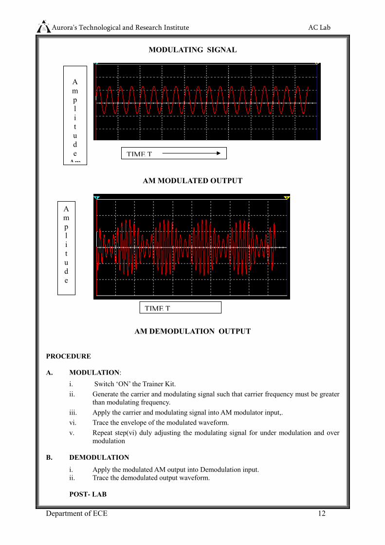
Auroras Technological and Research Institute AC Lab
Department of ECE 12
MODULATING SIGNAL
AM MODULATED OUTPUT
AM DEMODULATION OUTPUT
PROCEDURE
A MODULATION i Switch lsquoONrsquo the Trainer Kit
ii Generate the carrier and modulating signal such that carrier frequency must be greater than modulating frequency
iii Apply the carrier and modulating signal into AM modulator input vi Trace the envelope of the modulated waveform
v Repeat step(vi) duly adjusting the modulating signal for under modulation and over modulation
B DEMODULATION
i Apply the modulated AM output into Demodulation input ii Trace the demodulated output waveform
POST- LAB
TIME T
A
m
p
l i t u
d
e
Am
A
m
p
l i t u
d
e
TIME T
Auroras Technological and Research Institute AC Lab
Department of ECE 13
i Observe the frequency and amplitude of the carrier and modulating signal
ii Observe the frequency and maximum peak-peak amplitude(Amax) and minimum peak-
peak amplitude (Amin) of the AM signal in TableI
iii Calculate the modulation index Ч=Amax-AminAmax+Amin
iv Plot the out put waveforms Time T Vs Voltage Vo
v Write result and conclusion
CONCLUSION Hence the AM modulation and demodulation is verified
QUESTIONS 1 what is meant by modulation
2 What is meant by modulation index
3 What is meant by under modulation and over modulation
Auroras Technological and Research Institute AC Lab
Department of ECE 14
EXPERIMENT NO 2
DSB ndash SC Modulator amp Demodulator
OBJECTIVE To study the balanced modulator using IC 1496
PRE-LAB
1 Study the theory of balanced modulator
2 Draw the circuit diagram
3 Draw the expected waveforms
4 Study the datasheet of IC 1496
EQUIPMENT
1 Function generator
2 Dual trace CRO
3 Balanced modulator trainer kit
THEORY
In a balanced modulator a signal is modulated using two carriers that are 180
degrees out of phase The resulting signals are then combined in such a way that the carrier
components cancel leaving a DSB-SC (double sideband suppressed carrier) signal
CIRCUIT DIAGRAM
Auroras Technological and Research Institute AC Lab
Department of ECE 15
BALANCED MODULATOR OUTPUT
Auroras Technological and Research Institute AC Lab
Department of ECE 16
BALANCED DEMODULATOR OUTPUT
PROCEDURE
1 Switch ON the trainer kit
2 Generate the carrier and modulating signal
3 Apply the modulating signal and the carrier signal to the balanced modulator input
4 Observe the balanced modulator output
POST LAB
1 Observe the frequency and amplitude of the carrier and modulating signal
2 Observe the frequency and amplitude of the balanced modulator output
3 Observe the quadrature null effect
4 Plot the output waveforms Time T VS Voltage V
5 Write result and conclusions
CONCLUSIONS The balanced modulator output is verified
QUESTIONS 1 what is the efficiency for DSB SC signal
2 What are the other types of balanced modulators
3 What is meant by pilot carrier
Auroras Technological and Research Institute AC Lab
Department of ECE 17
EXPERIMENT NO 3
SSB ndash SC MODULATOR amp DEMODULATOR
OBJECTIVE To study the Single side band modulation by using Phase shift method and demodulation using synchronous detector method
PRE-LAB
1 Study the theory of SSB
2 Draw the circuit diagram and expected waveforms
EQUIPMENTS 1 Function generator 2
2 Dual trace CRO 1
3 SSB system modulation and demodulation trainer kit 4 Patch CardsConnecting wires
5 Frequency counterMulti meter
THEORY
Single-sideband modulation (SSB) is a refinement of amplitude modulation that more
efficiently uses electrical power and bandwidth It is closely related to vestigial sideband
modulation (VSB)Amplitude modulation produces a modulated output signal that has
twice the bandwidth of the original baseband signal Single-sideband modulation avoids
this bandwidth doubling and the power wasted on a carrier at the cost of somewhat
increased device complexity SSB was also used over long distance telephone lines as part
of a technique known as frequency-division multiplexing (FDM) FDM was pioneered by
telephone companies in the 1930s This enabled many voice channels to be sent down a
single physical circuit for example in L-carrier SSB allowed channels to be spaced
(usually) just 4000 Hz apart while offering a speech bandwidth of nominally 300ndash
3400 Hz Amateur began serious experimentation with SSB after World War II The
Strategic Air Command established SSB as the radio standard for its bombers in 1957[4]
It
has become a de facto standard for long-distance voice radio transmissions since then
Auroras Technological and Research Institute AC Lab
Department of ECE 18
BLOCK DIAGRAM OF SSB MODULATOR
SSB-DEMODULATOR SYSTEM
EXPECTED WAVEFORMS
Auroras Technological and Research Institute AC Lab
Department of ECE 19
DSB-SC 0UTPUT
SSB-SC OUTPUT
PROCEDURE
a Modulation
1 Switch ON the trainer kit 2 Observe the output of RF generator using CROThere are two outputs from the RF
generator one is direct output and another is 90 deg phase shift with the direct output 3 Observe the output of AF generator using CROThere are two outputs from the AF
generator one is direct output and another is 90 deg phase shift with the direct output 4 Set the amplitude of the RF signal to 01vpp and connect the 0 deg phase shift signal to
one BM and 90 deg angle phase shift signal to the second BM
5 Set the AF Signal amplitude to 8vpp and connect to the BM 6 Observe the outputs of both balanced modulators simultaneously and adjust the balance
control until get the output waveforms (DSB SC) 7 To get LSB of SSB connect both balanced modulators outputs to SUBTRACTED circuit 8 Measure the frequencies of LSB using multimeter 9 Calculate the theoretical frequency of the SSB (LSB) and compare it with the practical
value LSB=RE Frequency ndashAF Frequency
10 To get USB of SSB signal connect both balanced modulators outputs to ADDER circuit 11 Measure the frequencies of USB
12 Calculate the theoretical value of the SSB Upper Side Band (SSB-USB) frequency and compare it with practical value
USB=RF Frequency+AF Frequency
Auroras Technological and Research Institute AC Lab
Department of ECE 20
b Demodulation (Synchronous detector)
1 Connect the SSB signal from the summer or sub tractor to the SSB signal input of the synchronous detector and RF signal (0ordm) to the RF input of the synchronous detector
2 Observe the Detector output using CRO and compare it with the AF signal (Modulating Signal)
3 Observe the SSB signal for the different frequencies of the AF signal (modulating signal)
TABULATION RF Frequency (Fc) =--------------------KHz
USB LSB
SNo AFsig
Freq(Fm) Practical Freq Theoretical
Freq=Fc+Fm
Practical Freq
Theoretical Freq=Fc-Fm
POST LAB
1 Observe the frequency and amplitude of the RF carrier both (900 amp 0 0 ) phase AF modulating signal (900 amp 0 0 ) phase DSB-SC SSB-SC LSB and USB of the SSB signal
2 Observe the frequency components and bandwidth of SSB
3 Plot the output waveforms above mentioned 4 Write result and conclusion
CONCLUSIONS Hence various outputs of SSB modulator are obtained
QUESTIONS 1 What are the advantages of SSB over AM
2 What is the main drawback of SSB
3 What is meant by VSB
Auroras Technological and Research Institute AC Lab
Department of ECE 21
EXPERIMENT NO 4
FREQUENCY MODULATION AND DEMODULATION
OBJECTIVE To study
1 Frequency modulation process
2 Measurement of Modulation Index
3 Measurement of Frequency deviation
4 Demodulation Process
PRE-LAB 1 Study the data sheet of IC LM 2206 LM 565
2 Study the theory of FM modulation and demodulation
3 Draw the circuit diagram for modulation and demodulation
4 Draw the expected wave forms
EQUIPMENT 1 Frequency modulation and demodulation trainer kit 1 No 2 Dual trace CRO 1 No 3 Connecting probe and cords
THEORY
In telecommunications frequency modulation (FM) conveys information over a carrier
wave by varying its frequency (contrast this with amplitude modulation in which the amplitude
of the carrier is varied while its frequency remains constant) In analog applications the
instantaneous frequency of the carrier is directly proportional to the instantaneous value of the
input signal Digital data can be sent by shifting the carriers frequency among a set of discrete
values a technique known as keying The instantaneous frequency of the oscillator and is the
frequency deviation which represents the maximum shift away from fc in one direction
assuming xm(t) is limited to the range plusmn1Although it may seem that this limits the frequencies in
use to fc plusmn fΔ this neglects the distinction between instantaneous frequency and spectral
frequency The frequency spectrum of an actual FM signal has components extending out to
infinite frequency although they become negligibly small beyond a point Carsons rule of
thumb Carsons rule states that nearly all (~98) of the power of a frequency-modulated signal
lies within a bandwidth
Auroras Technological and Research Institute AC Lab
Department of ECE 22
CIRCUIT DIAGRAM
MODULATION
DEMODULATION
Auroras Technological and Research Institute AC Lab
Department of ECE 23
OUT PUT WAVEFORMS
Auroras Technological and Research Institute AC Lab
Department of ECE 24
PROCEDURE a Modulation
i Switch ON the trainer kit ii Generate the carrier and modulating signal iii apply the modulating signal to the frequency modulator iv Trace the FM output
b Demodulation i apply the modulated FM output into Demodulation input ii Trace the demodulated output waveform
TABULATION
SNo
Amplitude of Modulating
Signal(Am) Fmin
Frequency
Deviation
∆f=fc-fmin or fc-fmax
Modulation Index β=∆ffm
POST LAB
1 Observe the frequency and amplitude of the carrier and modulating signal 2 Calculate the frequency deviation by observing Fmax and Fmin
δ=Fc-Fmax or δ=Fc-Fmin
3 Calculate modulation index β= δFm
4 Change the amplitude of the modulating signal and repeat steps 1 to 3 for different values of Am and note down the readings in table-1
5 Plot the output waveforms Time T VS Voltage Vo
6 Write result and conclusion
CONCLUSIONS Hence the frequency modulated output is obtained
QUESTIONS 1 what is meant by angle modulation
2 How FM is different from AM
3 What is meant by Carson Rule
4 What is the maximum modulation index
Auroras Technological and Research Institute AC Lab
Department of ECE 25
EXPERIMENT NO 5
STUDY OF SPECTRUM ANALIZER AND ANALYSIS OF AM amp FM SIGNALS
Auroras Technological and Research Institute AC Lab
Department of ECE 26
Auroras Technological and Research Institute AC Lab
Department of ECE 27
Auroras Technological and Research Institute AC Lab
Department of ECE 28
EXPERIMENT NO 6
PRE EMPHASIS AND DE EMPHASIS
OBJECTIVE To study the operation of Pre-emphasis and De-emphasis circuits
PRE-LAB
1 Study the theory of Pre-emphasis and De-emphasis circuits
2 Draw the circuit diagram
3 Draw the expected waveforms
COMPONENTS
1 Resistors 100kΩ 100Ω
2 Capacitors 1μf 100μf EQUIPMENT 1 Function generator 1
2 Dual trace CRO 1
THEORY Pre-emphasis
Improving the signal to noise ratio by increasing the magnitude of higher frequency
signals with respect to lower frequency signals
De-emphasis
Improving the signal to noise ratio by decreasing the magnitude of higher
frequency signals with respect to lower frequency signals
Transmitters that employ a true FM modulator require a pre emphasis circuit before the
modulator fore the true FM modulator doesnt automatically pre emphasize the audio like
a transmitter that uses a phase modulator A separate circuit is not necessary for pre
emphasis in a transmitter that has a phase modulator because the phase modulator applies
pre emphasis to the transmitted audio as a function of the phase modulator The receivers
De emphasis circuitry takes the unnatural sounding pre emphasized audio and turns it
back into its original response Pre emphasized (discriminator) audio is however available
directly from the audio demodulation (discriminator) circuitry In linking systems many
choose to eliminate the emphasis circuitry to allow better representation of retransmitted
Auroras Technological and Research Institute AC Lab
Department of ECE 29
signals Since the signal has already been pre emphasized (by the user that is
transmitting) and since the receiver you are listening to takes care of the de emphasis
CIRCUIT DIAGRAMS
PRE-EMPHASIS
DE-EMPHASIS
EXPECTED WAVEFORMS
INPUT
TIME T
A
m
p
l i t u
d
e
Am
Auroras Technological and Research Institute AC Lab
Department of ECE 30
OUTPUT
PRE-EMPHASIS
Freq Vs Gain
DE-EMPHASIS
Freq Vs Gain
TIME T
Freq f (Hz)
A
m
p
l i t u
d
e
Am
Auroras Technological and Research Institute AC Lab
Department of ECE 31
TABLE
PRE EMPHASIS
SNo Input Freq
Input Voltage Vi (Volts)
Output Voltage Vo (Volts) Gain=VoVi
Gain in dB
20log(voVi)
DE-EMPHASIS
SNo Input Freq
Input Voltage Vi (Volts)
Output Voltage Vo (Volts)
Gain=VoVi Gain in dB
20log(VoVi)
PROCEDURE a Pre-emphasis
1 Connect the circuit as per the circuit diagram
2 Apply a constant sine wave input across the input terminal of fixed amplitude(Vi) 3 By varying the input frequency note down the output amplitude (Vo) with respect to
input frequency in Table 4 Calculate the gain using the formula
5 Gain =20log (Vo) (Vi) db
b De-Emphasis
1 Connect the circuit as per the circuit diagram
2 Repeat the steps 2 3 amp4
POST LAB
1 Observe the output amplitude for both the pre-emphasis and De-emphasis circuits
2 Calculate the gain in db
3 Plot the frequency versus gain curves on logarithmic graphs for both the circuits
4 Plot the input and output waveforms Time T VS Voltage Vo
5 Write the result and conclusion
CONCLUSIONS Obtained the pre emphasis and de-emphasis outputs
QUESTIONS 1 Observe the out put signal is disturbed by noise what action has to be taken and measure the
output voltage 2 Where we use the pre emphasis circuit 3 Where we use the de emphasis circuit 4 What are the advantages of pre emphasis and de emphasis circuits
Auroras Technological and Research Institute AC Lab
Department of ECE 32
EXPERIMENT NO 7
TIME DIVISION MULTIPLEXING AND DEMULTIPLEXING
AIM To study Time Division Multiplexing and its waveforms
PRE LAB WORK
Study the operation of Time division multiplexer and demultiplexer Draw the block diagram of TDM
Draw the expected graphs of all necessary waveforms ( CH1CH2TDM OP and Demultiplexed OP)
EQUIPMENT
1) Experimental board on TDM
2) Dual Trace CRO 3) Probes
THEORY
Time Division Multiplexing (TDM) is a technique for transmitting serial messages on a signal
transmission channel by dividing the time division into slots One slot for each message The concept
of TDM comes from sampling theorem which enables use to transmit the information contained in the
band limited Signal using sampling of the signal taken uniformly or a rate slightly higher then the
Nyquist rate TDM enables the joint utilization at a common transmission channel by a number of
independent message sources without mutual interference
The different Ip message signals all band limited in WHz by the IP low pass filters and sequentially
sampled at the transmitters by a rotary switch or a comparator The switch makes are complete
revolution in Ts frac12 W extracting are sample from each IP The commutator OP is a PAM waveform
containing individual message sample
It there are N number of IP the pulse to Pulse spacing will be Ts = 1 while the spacing
N Nfs
bw successive samples from each IP is called a frame
At the receiver a similar rotatory switch the decommutator separates the samples and distributes them
to a bank of low-pass filters which in turn is usually electronic and synchronization signals are
provided to keep the distribute in step with the commutant
Auroras Technological and Research Institute AC Lab
Department of ECE 33
EXPECTED GRAPHS
PROCUDURE
1 Connect the OP of the experimental board to one of the channels on CRO 2 Switch ON the experimental board 3 Observe the OP waveforms 4 Vary the values of the resistors R1 R2 and R3 alternative and observe the OP on CRO
RESULT
The process of the Time Division Multiplexing and the waveforms has been studied
CONCLUSION
Auroras Technological and Research Institute AC Lab
Department of ECE 34
Figure 1 Time Division Multiplexing amp De multiplexing
Auroras Technological and Research Institute AC Lab
Department of ECE 35
EXPERIMENT NO 9
VERIFICATION OF SAMPLING THEOREM
AIM To study the effect of sampling on the transmission of information through PWM
PRE LAB WORK
Study the sampling theorem
Draw the expected graphs of all necessary waveforms ( message signal carrier wave PWM op demodulated op etc
EQUIPMENT
1) Experimental Board on study of sampling theorem 2) Dual trace CRO (0 ndash 20 MHz) 3) Function Generator 4) Connecting wires
THEORY
The principle of sampling can be explained using the switching sampler The switch periodically shifts below bw two constants at the rate of fs = 1 Ts Hz staying on the IP constant for each sampling period The op Xs(t) of the samples consists of segments of x(t) and Xc(t) can be represented as
Xs(t) = X(t) S(t)
Where S(t) is sampling or switching function There are a number of differences bw the ideal sampling and reconstruction techniques described in the proceeding sections of the actual signal
PROCEDURE
1) Observe the internal clock and measure its frequency and amplitude 2) Give the clock to the clock IP terminal 3) Connect the modulating signal to the IP 4) Check the condition fs gt 2fm and observe the de-modulated wave 5) Check the condition fs lt 2fm and fs = 2fm and draw the OP waveforms
RESULT
CONCLUSION
Aurorarsquos Technological and Research Institute DC Lab
36
Figure 2 Sampling Theorem
Aurorarsquos Technological and Research Institute DC Lab
37
EXPERIMENT NO 10
PULSE AMPLITUDE MODULATION AND DEMODULATION
AIM 1) To study the PAM modulation and its waveforms
2) To study the de-modular of PAM
3) To study the effect of sampling frequency on de-modulation OP
PRE LAB WORK
Study the operation Pulse Amplitude Modulator and Demodulator Draw the block diagram of PAM modulator and demodulator Draw the expected graphs of all necessary waveforms ( message signal carrier wave PAM op
demodulated op etc)
EQUIPMENT
1) Exp Board on study of PAM 2) CRO 3) Functional Generator 4) Connecting wires and chords
THEORY
In PAM the amplitude of the carrier wave of higher frequency follow the amp of the message signal
Within this (Modulation Sampling) we have two more types of sampling those are
(1) Natural Sampling
(2) Flat Top Sampling
Basically in Natural Sampling the carrier waves are train of pulses of a certain frequency After
sampling the top of the Pulse follow the message signal Due to this following of top of Pulses with the
message signals cause a distortion in De-modulation
In Flat top sampling also we use train of pulses for sampling but only the starting point of each pulse
follow the message signal remaining width of the pulse will (follow) be flat But here we go for Natural
sampling
EXPECTED WAVEFORMS
Aurorarsquos Technological and Research Institute DC Lab
38
PROCEDURE (MODULATION)
1 Observe the clock on CRO and measure its frequency and amp (freq 5KHz) 2 Connect the clock to clock IP terminals in modulation 3 Put control switch in ac position and set amplitude = OV This provides DC at Modulating
signal terminal 4 Connect the modulating signal or IP to the modulator 5 Connect one channel of CRO at lsquoTirsquo and Gnd Observe that the pulses are of same height
Height is adjustable by varying offset This is PAM signal with DC IP Measure amplitude and frequency of Pulses
6 Increase the amplitude of modulation signal Observe the amplitude and frequency of this sinusoidal modulating signal
7 Observe PAM signal
a) How many Pulses are there in one modulating cycle
b) It is natural or Flat Top PAM c) It is Single or dual polarity PAM
8 Observe the effect of DC offset on PAM waveform
DE-MODULATION
1) Generate undistorted PAM waveform 2) Connect the modulating signal to de-modulation IP 3) Observe the detected OP and measure its frequency which must be same as
modulating signal
EFFECT OF SAMPLING FREQUENCY
1) Connect internal sinusoidal signal to modulating signal IP of the modulator 2) Connect an external functional Generator at the circuit terminals of the modulator 3) Get the PAM waveform using the above circuit 4) Adjust the modulating amplitude offset and frequency to get an undistorted frequency 5) Connect the PAM to de-modulator IP 6) Observe the demodulated signal for various frequencies of clock (fs gt 2fm lt 2fm = 2 fm)
RESULT
CONCLUSION
Aurorarsquos Technological and Research Institute DC Lab
39
Figure 3 Pulse Amplitude Modulation
Auroras Technological and Research Institute AC Lab
Department of ECE 5
EXPERIMENT NO 11
PULSE WIDTH MODULATION AND DEMODULATION
AIM
1) To study the PWM process and the corresponding waveforms 2) To study the effect of sampling frequency on the transmission of information through PWM
PRE LAB WORK
Study the operation Pulse Width Modulator and Demodulator Draw the block diagram of PWM modulator and demodulator Draw the expected graphs of all necessary waveforms ( message signal carrier wave PWM op
demodulated op etc
EQUIPMENT
1) Experimental Board
2) Dual trace CRO 3) AF generator 4) Multimeter
THEORY
In PWM the samples of the message signal are used to vary the duration of the individual pulses The
pulse width may be varied by varying the time of occurrence of the leading edge trailing edge of both
edges of the pulse in accordance with the sampled value of the modulating wave PWM can also be
generated by using emitter follower monostable multivibrator is an excellent voltage to time converter
since its gate width is dependent on the voltage to which the capacitor is changed If this voltage can be
varied in accordance with a signal voltage a series of rectangular pulses can be obtained with width
varying as required
The demodulated of PWM is quite simple PWM is passed through a low pass filter The reconstruction is
associated with a certain amount of Distortion caused by the cross modulator products that fall in the
signal band
EXPECTED WAVEFORM
Aurorarsquos Technological and Research Institute DC Lab
41
PROCEDURE
STUDY OF MODULATION
1) Observe the clock on CRO and measure its frequency (fs) 2) Observe the sine wave modulating signal on CRO and observe the dc shift produced in this
by varying the offset nob Measure the frequency Variation limits of this signal 3) Apply clock at the circuit input terminal 4) Apply modulating signal by keeping the control switch in dc position 5) Observe the modulated wave 6) Plot the graph bw pulse width and the applied dc voltage 7) Put the control switch in sine wave position and adjust the modulating signal amplitude
frequency and dc offset to get the stationary waveform of PWM 8) Note the number of pulses in one circuit of modulating signal
STUDY OF DEMODULATION
1) Generate the stationary PWM waveform using sin wave modulating signal 2) Connect the modulator OP to PWM demodulator 3) Connect Channel (1) to Modulating Signal and channel (2) to demodulated wave
EFFECT OF SAMPLING FREQUENCY
1) Use an external square wave and connect it to the clock input 2) Set the frequency of square wave at frequency 2fm 3) Observe the demodulated wave
4) Change the frequency of square wave to fs lt 2fm fs gt 2fm and observe the demodulated wave
RESULT
CONCLUSION
Aurorarsquos Technological and Research Institute DC Lab
42
Figure 4 Pulse Width Modulation
Aurorarsquos Technological and Research Institute DC Lab
43
EXPERIMENT NO 12
PULSE POSITION MODULATION AND DEMODULATION
AIM
1) To study the PPM Modulation and the corresponding waveforms 2) To study the de-modulation of PPM 3) To see the effect of sampling frequency on the transmission of information through PPM
PRE LAB WORK
Study the operation Pulse Position Modulator and Demodulator Draw the block diagram of PPM modulator and demodulator Draw the expected graphs of all necessary waveforms ( message signal carrier wave PPM op
demodulated op etc
EQUIPMENT
1) Experimental Board for PPM
2) Dual Phase Oscilloscope
3) AF Generator
THEORY
In PDM long pulses expand considerable power duration If the pulse which bearing no additional
information If this un used power is subtracted from PDM so that only time transitions are preserved
We observe a more efficient type of pulse modulation known as pulse position modulation Here in the
Pulse Position Modulated wave the position of the Pulse relative to its unmodulated time of occurrence is
varied in accordance with the message signal
We generate a PPM wave from PWM wave by using a Monostable Multivibrator The device has one
absolutely stable state and one quest ndash stable state into which it is triggered by an externally applied Pulse
The monostable multivibrator is designed to trigger on the trailing edges of the duration ndash modulated pulse
is varied in accordance with the message signal
The fixed pulse duration of the PPM wave at the monostable multivibrator OP can be set by appropriately
choosing the resistance ndash capacitance combination in the timing circuit of the device
Aurorarsquos Technological and Research Institute DC Lab
44
EXPECTED WAVEFORM
PROCEDURE
STUDY OF MODULATION
Observe the clock and measure its frequency (fs) Apply the clock at the clock IP terminal in the modulator Apply the modulating signal keeping control switch in DC position Observe the PPM OP Connect the channel ndash (1) on CRO to clock and channel (2) to PPM wave OP Compare the position of two waveforms Vary the DC offset and observe the relative shift between the clock and PPM OP Measure the time shift between clock and PPM wave for various settings of offset Draw the graph between time shift and DC voltage Put the control switch in AC position adjusts the amplitude and frequency and offset
of sinusoidal modulating signal to get the stationary PPM wave Note the number of pulses in one cycle of the modulated wave
STUDY OF DEMODULATION
Generate a stationery PPM wave for a sinusoidal modulating signal Apply the PPM wave to the input of de-modulator Connect the Channel ndash (1) of CRO to the modulating signal and channel ndash 2 to the
de-modulator output Compare the two waveforms
Note the frequency of demodulated wave It should be same as the modulating signal Note down the waveform
RESULT
CONCLUSION
Aurorarsquos Technological and Research Institute DC Lab
45
Aurorarsquos Technological and Research Institute DC Lab
46
Figure 5 Pulse Position Modulation
Aurorarsquos Technological and Research Institute AC Lab
47
EXPERIMENT NO 13
FREQUENCY SYNTHESIZER
AIM
To study the operation of frequency synthesizer using PLL
PRE-LAB 1 Study the data sheet of IC 7404IC 4017IC 565 and IC 4046
2 Study the theory of frequency synthesizer 3 Draw the circuit diagram and expected waveforms
EQUIPMENTS
1 Frequency synthesizer trainer AET -26A
2 Dual trace CRO (20Mhz) 3 Digital frequency counter or multimeter
4 Patch chords
THEORY
A frequency synthesizer is an electronic system for generating any of a range
of frequencies from a single fixed time base or oscillator They are found in many modern
devices including radio receivers mobile telephones radiotelephones walkie-talkies CB
radios satellite receivers GPS systems etc A frequency synthesizer can combine
frequency multiplication frequency division and frequency mixing (the frequency mixing
process generates sum and difference frequencies) operations to produce the desired output
signal
BLOCK DIAGRAM
Phase Comparator
Amplifier Low pass filter
V C O
Div N Network frequency divider
Fin= fout
N
fin
Fout =Nf in
Aurorarsquos Technological and Research Institute AC Lab
48
SIMPLE 1KHZ-9KHZ FREQUENCY SYNTHESIZER
CIRCUIT DAIGRAM
PROCEDURE 1 Switch on the trainer ad verify the output of the regulated power supply ie 5V These
supplied are internally connected to the circuit so no extra connections are required 2 Observe output of the square wave generator using oscilloscope and measure the range
with the help of frequency counter frequency range should be around 1KHz to 10KHz 3 Calculate the free running frequency range of the circuit (VCO output between 4th pin
and ground 1 For different values of timing resistor R1 ( to measure Rt value using digital multimeter between given test points 1 And record the frequency values in table 1
Fout = 03 (RtCt) where Rt is the timing resistor and Ct is the timing capacitor = 001 f
Aurorarsquos Technological and Research Institute AC Lab
49
4 Connect 4th pin of LM 565 (Fout) to the driver stage and 5th pin (Phase comparator) connected to 11th pin of 7404 Output can be taken at the 11th pin of the 7490 It should be divided by the 2 amp 3 times of the fout
TABULATION
Fin KHz Fout = N x fin KHz Divided by 3 2
EXPECTED WAVEFORMS
POST LAB
1 Observe the synthesized output in table 2 Calculate the output frequency
3 Plot the output waveforms
4 Write result and conclusions
CONCLUSIONS
The various outputs of frequency synthesizer are verified
QUESTIONS
1 What are the applications of frequency synthesizer
TIME T
A
m
p
l i T
u
d
e
Ac
Aurorarsquos Technological and Research Institute AC Lab
50
2 What is the difference between heterodyning and synthesizer
Aurorarsquos Technological and Research Institute AC Lab
51
EXPERIMENT NO 14
AGC CHARATERISTICS
AIM
To observe the effect of automatic gain control(AGC)
PRE LAB 1 To study the theory of AGC 2 Draw the Block Diagram circuits diagram and expected waveforms
EQUIPMENTS 1 AGC Trainer Kit 2 CRO
3 Patch Chords
4 Digital Multimeter
THEORY
Automatic gain control (AGC) is an adaptive system found in many electronic
devices The average output signal level is fed back to adjust the gain to an appropriate level
for a range of input signal levels For example without AGC the sound emitted from an AM
radio receiver would vary to an extreme extent from a weak to a strong signal the AGC
effectively reduces the volume if the signal is strong and raises it when it is weaker AGC
algorithms often use a PID controller where the P term is driven by the error between
expected and actual output amplitude
Block Diagram
Frequency Converter
1st IF Amplifier
2nd IF Amplifier
Detector
Audio Preamplifier
Driver Output
Aurorarsquos Technological and Research Institute AC Lab
52
CIRCUIT DIAGRAM
PROCEDURE
1 Connect 455 KHz IF Signal Function Generator connect AGC link Connect CRO channel-1 at input terminals
2 Connect CRO channel 2 at collector of Q3 The amplified signal will be observed 3 Calculate the voltage gain by measuring the amplitude of output signal (Vo) waveform
using formula A=VoVi 4 Now connect CRO-2 channel at output The detected audio signal of 455 Khz will be
observed 5 Now vary input level of 455 KHz IF signal and observe detected 455 KHz audio signal
with and without AGC link The output will be distorted when AGC link is removed ie there is no AGC action
6 This explains AGC effect in Radio circuit
TABULATION
SNo Input Voltage Vi (P-P) With out AGC With AGC
Output Voltage Vo (P-P)
Gain A= Vo Vi
Output Voltage Vrsquoo (P-P)
Gain Arsquo= Vrsquoo Vi
Aurorarsquos Technological and Research Institute AC Lab
53
EXPECTED WAVEFORMS
AM Modulated RF Input
Detected Output with AGC
Detected Output without AGC
POST-LAB
1 Observe the input voltage and output voltage for with AGC and Without AGC in Table 1
2 Calculate Gain a=vovi for both cases 3 Plot the output waveforms Time T Vs Voltage Vo and input voltage Vi Vs Gain A 4 Write Result and Conclusions
CONCLUSIONS The AGC characteristics are verified
QUESTIONS 1 what is meant by AGC
2 What is the difference between simple AGC and delayed AGC
3 From which part of receiver AGC is obtained
TIME T
A
m
p
l i T
u
d
e
Ac
TIME T
A
m
p
l i T
u
d
e
Ac
TIME T
A
m
p
l i T
u
d
e
Ac
Aurorarsquos Technological and Research Institute AC Lab
54
EXPERIMENT NO 15
PHASE LOCKED LOOP
OBJECTIVE To study the Phase locked loop using 565 IC and to take input frequency given by an external signal source
PRE-LAB To Study
1 The data sheet of IC 565
2 The theory of Phase locked loop
3 About free running frequency locking range and capture range
4 Draw the circuit diagram and expected waveforms
EQUIPMENT 1 Function generator 2
2 Dual trace CRO 1
3 Phase locked loop trainer kit
THEORY
A phase-locked loop or phase lock loop (PLL) is a control system that generates a signal
that has a fixed relation to the phase of a reference signal A phase-locked loop circuit
responds to both the frequency and the phase of the input signals automatically raising or
lowering the frequency of a controlled oscillator until it is matched to the reference in both
frequency and phase A phase-locked loop is an example of a control system using negative
feedback Phase-locked loops are widely used in radio telecommunications computers and
other electronic applications They may generate stable frequencies recover a signal from a
noisy communication channel or distribute clock timing pulses in digital logic designs
such as microprocessors Since a single integrated circuit can provide a complete phase-
locked-loop building block the technique is widely used in modern electronic devices
with output frequencies from a fraction of a cycle per second up to many gigahertz
BLOCK DIAGRAM
Aurorarsquos Technological and Research Institute AC Lab
55
CIRCUIT DIAGRAM
PROCEDURE 1 Switch ON the trainer kit 2 Check the VCO output at pin 4 of IC 565 that is a square wave form The frequency of the
VCO Output depends on CT (001f) and RT (47kΩ) 3 Next short the pins 4amp5 and give signal of variable frequency and observe VCO output 4 Change the input frequency and observe the VCO output on the CRO 5 Between some frequencies the VCO output is locked to the input signal frequency This can
be observed by increasing or decreasing the frequency of the VCO output by changing input frequency
6 Before or after that frequency range the VCO output is not locked
7 Calculate Lock range (FL) and capture range (FC) by using the following formulas
FL = 8foVCO fo=03RtCT
FC=12π radic2πf236103 C2
Table1
SNo Locking Frequency Frequency Range From To
CHARTERISTICES
Aurorarsquos Technological and Research Institute AC Lab
56
CONCLUSIONS Obtained the lock range of PLL
QUESTIONS
1 Observe the VCO output when pins 4amp5 short and give square wave as signal 2 Define lock range and capture range
3 What are the basic applications of PLL
Aurorarsquos Technological and Research Institute AC Lab
57
ANNEXURE-I
EXPERIMENT NO 1
Aurorarsquos Technological and Research Institute AC Lab
58
CHARACTERISTICS OF MIXER
AIM
To study the functioning of a frequency mixer
PRE LAB 1 To study the theory of Mixer 2 Draw the circuit diagram and expected waveforms
EQUIPMENTS 1 Frequency mixer trainer kit 2 CRO (20MHz) 3 Connecting cords and probes 4 Function generator (1MHz)
THEORY
In receivers using the super heterodyne principle a signal at variable frequency is
converted to a fixed lower frequency IF before detection IF is called the intermediate frequency
In typical AM (Amplitude Modulation eg as used on medium wave) home receivers that
frequency is usually 455 kHz for FM VHF receivers it is usually 107 MHz An intermediate
frequency (IF) is a frequency to which a carrier frequency is shifted as an intermediate step in
transmission or reception Frequency modulation (FM) is a form of modulation that represents
information as variations in the instantaneous frequency of a carrier wave Very high frequency
(VHF) is the radio frequency range from 30 MHz (wavelength 10 m) to 300 MHz (wavelength 1
heterodyne receivers mix all of the incoming signals with an internally generated waveform
called the local oscillator The user tunes the radio by adjusting the sets oscillator frequency in
the mixer stage of a receiver the local oscillator signal multiplies with the incoming signals
which shifts them all down in frequency The one that shifts is passed on by tuned circuits
amplified and then demodulated to recover the original audio signal The oscillator also shifts a
copy of each incoming signal up in frequency by amount Those very high frequency images
are all rejected by the tuned circuits in the IF stage The Super heterodyne receiver (or to give it its
full name The Supersonic Heterodyne Receiver usually these days shortened to superhet) was
invented by Edwin Armstrong in 1918
Aurorarsquos Technological and Research Institute AC Lab
59
BLOCK DIAGRAM
CIRCUIT DIAGRAM
EXPECTED WAVEFORMS
INPUT SIGNAL Fx
INPUT SIGNAL Fy
TIME T
A
m
p
l i T
u
d
e
Ac
Aurorarsquos Technological and Research Institute AC Lab
60
MIXER OUTPUT(Fy-Fx)
PROCEDURE 1 Connect the circuit as per the given circuit diagram 2 Switch on the power supply of trainer kit 3 Apply a sine wave at input Fx of 2 VP-P amplitude and 100 KHz frequency 4 Apply a sine wave at input FY of 2 VP-P amplitude and 100 KHz frequency 5 Observe the output waveform on the CRO 6 Repeat the steps 34 and 5 by changing the values of Fx once greater than and less than
FY in a steps of 5Khz (in the range 80KHz to 120KHz)
TABULATION
TIME T
A
M
P
L
I T
U
D
E
TIME T
A
m
p
l i T
u
d
e
Ac
Aurorarsquos Technological and Research Institute AC Lab
61
SNo Freq (Fy)
(kHz) Amp(V) Freq(Fx) (kHz) Amp(V) Freq(Fy-Fx)
(kHz) Amp(V)
POST LAB 1 Observe the amplitude and time Of inputs and output in table
2 Draw the expected waveforms
3 Verify the output signal obtained with the theoretical value 4 Plot the graphs for Time T VS input signal (FX) Voltage V input signal (FY) Voltage V
and output Signal F(x-y) voltage V 5 Write result and conclusions
CONCLUSIONS
Obtained the output of the mixer for various inputs
QUESTIONS
1 what are the different types of mixtures available
2 What is meant by heterodyning
3 What is meant by IF
Aurorarsquos Technological and Research Institute AC Lab
62
EXPERIMENT NO 2
DIGITAL PHASE DETECTOR
OBJECTIVE To detect the phase difference between two square wave signals using digital phase detector
PRE LAB
1 To study the theory of digital phase detector and EX-OR gate operation and truth table 2 Draw the circuit diagram and expected output and input waveforms
EQUIPMENT 1 Digital phase detector trainer kit 2 Regulated power supplies
3 CRO (20MHz) 4 Connecting cords amp probes
5 Digital frequency counter or multimeter
THEORY
Phase detector is a frequency mixer or analog multiplier circuit that generates a voltage
signal which represents the difference in phase between two signal inputs It is an essential
element of the phase-locked loop (PLL)Detecting phase differences is very important in many
applications such as motor control radar and telecommunication systems servo mechanisms and
demodulators
Electronic phase detector
Some signal processing techniques such as those used in radar may require both the amplitude
and the phase of a signal to recover all the information encoded in that signal One technique is to
feed an amplitude-limited signal into one port of a product detector and a reference signal into the
other port the output of the detector will represent the phase difference between the signals If the
signal is different in frequency from the reference the detector output will be periodic at the
difference frequency Phase detectors for phase-locked loop circuits may be classified in two
types A Type I detector is designed to be driven by analog signals or square-wave digital signals
and produces an output pulse at the difference frequency The Type I detector always produces an
output waveform which must be filtered to control the phase-locked loop variable frequency
oscillator (VCO) A type II detector is sensitive only to the relative timing of the edges of the input
and reference pulses and produces a constant output proportional to phase difference when both
signals are at the same frequency This output will tend not to produce ripple in the control voltage
of the VCO
Aurorarsquos Technological and Research Institute AC Lab
63
BLOCK DIAGRAM OF PLL
CIRCUIT DIAGRAM
Aurorarsquos Technological and Research Institute AC Lab
64
EXPECTED WAVEFORMS
EX-OR PHASE DETECTOR
EDGE TRIGGERED OUTPUT
PROCEDURE
1 Switch on the trainer kit
2 Observe the output of the square wave generator available on the trainer kit using CRO
and measure the range with the help of frequency counter the frequency range should be
around 2 KHz to 13 KHz
3 Calculate the free running range of the VCO output ie between 4th pin of IC PLL 565
and ground For different values of timing resistor Rt fout is given by Fout =03 Rt Ct
where Ct timing capacitor = 001 μF Rt timing resistor
4 Connect the square wave to the input of IC PLL 565 and short 4th and 5th pin of PLL
Vary the input frequency of the square wave when the PLL is locked that is connected to
Aurorarsquos Technological and Research Institute AC Lab
65
one input fout EX-OR phase detector The other input fin of EX-OR phase detector is the
coming from inbuilt of square wave generator
5 Connect the pulse generator output to the input of IC 565 PLL and short 4th amp 5th pin of
PLL Vary the input frequency of the square wave when the PLL is locked that is
connected to one input of Edge triggered phase detector input ie fout The other input fin
of edge triggered phase detector is the pulse input coming from the inbuilt pulse generator
6 The dc output voltage of the exclusive-OR phase detector is a function of the phase
difference between its two inputs fin and fout
POST LAB
1 Observe the Voltage and Time of the two input square waves
2 Observe difference of two inputs as square wave output
3 Plot the inputs and output waveforms Time T VS Voltage V
CONCLUSIONS
The phase detector outputs are verified
QUESTIONS
1 What is the function of phase detector
2 What is the condition for getting maximum output
3 Advantages of digital phase detector over analog phase detector
Aurorarsquos Technological and Research Institute AC Lab
66
EXPERIMENT NO 3
COASTAS RECEIVER
AIM
To demodulate a DSB-SC signal using coastas receiver
PRE LAB 1 To study the operation of coastas receiver 2 Draw the circuit diagram and expected waveforms
EQUIPMENTS 1 Communications trainer kit 2 DSB-SC modulator trainer kit 3 CRO (20MHz) 4 Connecting cords and probes 5 Function generator (1MHz)
THEORY
This loop and its variations is much-used as a method of carrier acquisition (and
simultaneous message demodulation) in communication systems both analog and digital
It has the property of being able to derive a carrier from the received signal even when there is
no component at carrier frequency present in that signal (eg DSBSC) The requirement is that
the amplitude spectrum of the received signal be symmetrical about this frequency
The Costas loop is based on a pair of quadrature modulators - two multipliers
fed with carriers in phase-quadrature These multipliers are in the in-phase (I) and quadrature
phase (Q) arms of the arrangement Each of these multipliers is part of separate synchronous
demodulators The outputs of the modulators after filtering are multiplied together in a third
multiplier and the lowpass components in this product are used to adjust the phase of the local
carrier source - a VCO - with respect to the received signal The operation is such as to
maximise the output of the I arm and minimize that from the Q arm The output of the I arm
happens to be the message and so the Costas loop not only acquires the carrier but is a
(synchronous) demodulator as well A complete analysis of this loop is non-trivial It would
include the determination of conditions for stability and parameters such as lock range capture
range and so on
Aurorarsquos Technological and Research Institute AC Lab
67
BLOCK DIAGRAM
EXPECTED WAVEFORMS
DSB-SC modulated output
Aurorarsquos Technological and Research Institute AC Lab
68
Demodulated output of the coastas loop
PROCEDURE
1 Switch ON the DSB-SC trainer kit
2 Generate the carrier and modulating signal
3 Generate the DSB-SC modulated signal
4 Connect the required blocks of the coastas receiver in the communications kit
5 Apply the generated DSB-SC signal to the above connected coastas receiver
6 Observe that the output of the coastas receiver is the demodulated wave of DSB-SC signal
POST LAB
1 Observe the frequency and amplitude of the carrier and modulating signal
2 Observe the frequency and amplitude of the balanced modulator output
3 Observe the lock condition of the coastas loop
4 observe the output of the coastas demodulator
5 Write result and conclusions
CONCLUSIONS The balanced modulator output and the operation of coastas receiver is verified
QUESTIONS 1 what is the operation of coastas loop
2 What happens when the locking condition of the coastas loop occurs
3 Coastas loop can be used for demodulation of other modulation techniques also What are they
Aurorarsquos Technological and Research Institute AC Lab
69
MATLAB PROGRAMMES
Aurorarsquos Technological and Research Institute AC Lab
70
INDEX
1 Introduction - 70
2 Amplitude Modulation and Demodulation - 74
3 DSB-SC Modulation and Demodulation - 84
4 SSB-SC Modulation and Demodulation - 89
5 Frequency Modulation and Demodulation - 95
6 Phase Modulation and Demodulation - 99
7 Time Division Multiplexing and Demultiplexing - 100
8 Frequency Division Multiplexing and Demultiplexing- 103
9 Verification of Sampling Theorem - 104
10 Pulse Amplitude Modulation and Demodulation - 106
11 Pulse width Modulation and Demodulation - 108
12 Pulse Position Modulation and Demodulation - 110
13 PLL as FM Demodulator - 112
Aurorarsquos Technological and Research Institute AC Lab
71
1 INTRODUCTION
What Is Simulink
Simulink is a software package for modeling simulating and analyzing dynamic
systems It supports linear and nonlinear systems modeled in continuous time sampled time
or a hybrid of the two Systems can also be multirate ie have different parts that are
sampled or updated at different rates
Tool for Simulation
Simulink encourages you to try things out You can easily build models from scratch
or take an existing model and add to it You have instant access to all the analysis tools in
MATLABreg so you can take the results and analyze and visualize them A goal of Simulink
is to give you a sense of the fun of modeling and simulation through an environment that
encourages you to pose a question model it and see what happens
Simulink is also practical With thousands of engineers around the world using it to
model and solve real problems knowledge of this tool will serve you well throughout your
professional career
Tool for Model-Based Design
With Simulink you can move beyond idealized linear models to explore more realistic
nonlinear models factoring in friction air resistance gear slippage hard stops and the other
things that describe real-world phenomena Simulink turns your computer into a lab for
modeling and analyzing systems that simply wouldnt be possible or practical otherwise
whether the behavior of an automotive clutch system the flutter of an airplane wing the
dynamics of a predator-prey model or the effect of the monetary supply on the economy
For modeling Simulink provides a graphical user interface (GUI) for building models
as block diagrams using click-and-drag mouse operations With this interface you can draw
the models just as you would with pencil and paper (or as most textbooks depict them) This
is a far cry from previous simulation packages that require you to formulate differential
equations and difference equations in a language or program Simulink includes a
comprehensive block library of sinks sources linear and nonlinear components and
connectors You can also customize and create your own blocks For information on creating
your own blocks see the separate Writing S-Functions guide
Models are hierarchical so you can build models using both top-down and bottom-up
approaches You can view the system at a high level then double-click blocks to go down
through the levels to see increasing levels of model detail This approach provides insight into
how a model is organized and how its parts interact
After you define a model you can simulate it using a choice of integration methods either
from the Simulink menus or by entering commands in the MATLAB Command Window The
menus are particularly convenient for interactive work while the command-line approach is
very useful for running a batch of simulations (for example if you are doing Monte Carlo
simulations or want to sweep a parameter across a range of values) Using scopes and other
display blocks you can see the simulation results while the simulation is running In addition
Aurorarsquos Technological and Research Institute AC Lab
72
you can change many parameters and see what happens for what if exploration The
simulation results can be put in the MATLAB workspace for post processing and
visualization
Model analysis tools include linearization and trimming tools which can be accessed
from the MATLAB command line plus the many tools in MATLAB and its application
toolboxes And because MATLAB and Simulink are integrated you can simulate analyze
and revise your models in either environment at any point
1 Generation of cosine wave in time domain and frequency
domain Clc clear all close all x = -500015 t = 0140001 time = cos(23141000t) y1 = cos(23141000x) subplot(211) plot(xy1) axis([-5 5 -3 3]) grid on title(Time domain) xlabel(Time ) ylabel(Amplitude) now create a frequency vector for the x-axis and plot the magnitude and phase subplot(212) fre = abs(fft(time)) f = (0length(fre) - 1)4000length(fre) plot(ffre) grid on title(Frequency domain (Spectrum)) xlabel(Freq ) ylabel(Amplitude)
WAVEFORMS
Aurorarsquos Technological and Research Institute AC Lab
73
2 Generation of square wave in time domain and frequency
domain
clc clear all close all x = -500015 Fs = 399 t = 01Fs1 time = SQUARE(2pi1000t) y1 = SQUARE(23141000x) subplot(211) plot(xy1) axis([-5 5 -3 3]) grid on xlabel(Time domain) ylabel(Amplitude) now create a frequency vector for the x-axis and plot the magnitude and phase subplot(212) fre = abs(fft(time)) f = (0length(fre) - 1)Fslength(fre) plot(ffre) grid on xlabel(Freq domain) ylabel(Amplitude)
WAVEFORMS
Aurorarsquos Technological and Research Institute AC Lab
74
Aurorarsquos Technological and Research Institute AC Lab
75
2 AMPLITUDE MODULATION AND DEMODULATION PROGRAM 1
clc clear all close all Ac=1 Carrier Amplitude Fc=04 Carrier frequency Fm=005 baseband frequency Fs=10 sampling t=001200 mt=cos(2piFmt) under modulation mu=05 st=Ac(1+mumt)cos(2piFct) subplot(211) plot(tst) hold on plot(tAc(mumt+ones(1length(mt)))r) plot(t-Ac(mumt+ones(1length(mt)))r) hold off title(Modulation Index = 05 under modulation Ac(1+05cos(2pi005t))cos(2pi04t)) xlabel(time (s))ylabel(amplitude) st_fft=fft(st) st_fft=fftshift(st_fft) st_fft_fre=5linspace(-11length(st_fft)) subplot(212) plot(st_fft_freabs(st_fft)) title(spectrum with Modulation Index = 05) xlabel(Frequency (Hz))axis([-1 1 0 1000Ac+100])
total modulation figure mu=1 st=Ac(1+mumt)cos(2piFct) subplot(211) plot(tst) hold on plot(tAc(mumt+ones(1length(mt)))r) plot(t-Ac(mumt+ones(1length(mt)))r) hold off title(Modulation Index = 1 modulation Ac(1+1cos(2pi005t))cos(2pi04t)) xlabel(time (s))ylabel(amplitude) st_fft=fft(st) st_fft=fftshift(st_fft) st_fft_fre=Fs2linspace(-11length(st_fft)) subplot(212) plot(st_fft_freabs(st_fft)) title(spectrum with Modulation Index = 1) xlabel(Frequency (Hz))axis([-1 1 0 1000Ac+100])
Aurorarsquos Technological and Research Institute AC Lab
76
over Modulation figure mu=2 st=Ac(1+mumt)cos(2piFct) subplot(211) plot(tst) hold on plot(tAc(mumt+ones(1length(mt)))r) plot(t-Ac(mumt+ones(1length(mt)))r) hold offtitle(Modulation Index = 2 over modulation Ac(1+2cos(2pi005t))cos(2pi04t)) xlabel(time (s))ylabel(amplitude) st_fft=fft(st) st_fft=fftshift(st_fft) st_fft_fre=Fs2linspace(-11length(st_fft)) subplot(212) plot(st_fft_freabs(st_fft)) title(spectrum with Modulation Index = 2) xlabel(Frequency (Hz))axis([-1 1 0 1000Ac+100])
WAVEFORMS
Aurorarsquos Technological and Research Institute AC Lab
77
PROGRAM 2
Aurorarsquos Technological and Research Institute AC Lab
78
task 1 fc=154000
task 2 fm=fc10 fs=100fc t=01fs4fm xc=cos(2pifct) xm=cos(2pifmt) figure(1) subplot(211)plot(txc) title(carrier signal of 154 khz) xlabel(time (sec)) ylabel(amplitude) subplot(212)plot(txm) title(message signal of 154 khz) xlabel(time (sec)) ylabel(amplitude) DSB-SC MODULATION mu = input( enter the Modulation Index value ) z1=(1+muxm)xc figure(2)
task 31 subplot(211)plot(tz1) title(AMPLITUDE MODULATION IN TIME DAOMAIN) xlabel(time (sec)) ylabel(amplitude)
task 32 l1=length(z1) f=linspace(-fs2fs2l1) Z1=fftshift(fft(z1l1)l1) subplot(212)plot(fabs(Z1)) title(AMPLITUDE MODULATION IN FREQUENCY DOMAIN) xlabel(frequency(hz)) ylabel(amplitude) axis([-200000 200000 0 03])
task 33 demodulation s1=z1xc S1=fftshift(fft(s1length(s1))length(s1)) figure(3) plot(fabs(S1)) title( demodulated signal IN FREQUENCY DOMAIN before filtring) xlabel(frequency(hz)) ylabel(amplitude) axis([-200000 200000 0 03]) hold on Hlp=1sqrt(1+(ffc)^(2100)) plot(fHlpr) title( frequency response of low pass filter) xlabel(frequency(hz)) ylabel(amplitude) axis([-200000 200000 0 2])
task 34 E1=HlpS1 figure(4) subplot(211)plot(fE1)
Aurorarsquos Technological and Research Institute AC Lab
79
title( Recover signal IN FREQUENCY DOMAIN after filtring) xlabel(frequency(hz)) ylabel(amplitude) axis([-200000 200000 0 03]) e1=ifft(ifftshift(E1))length(E1) subplot(212)plot(t(105)e1) title( Recover signal IN Time DOMAIN after filtring) xlabel(time(sec)) ylabel(amplitude)
WAVEFORMS
enter the Modulation Index value 05
0 1 2 3
x 10-4
-1
-05
0
05
1carrier signal of 154 khz
time (sec)
am
plit
ude
0 1 2 3
x 10-4
-1
-05
0
05
1message signal of 154 khz
time (sec)
am
plit
ude
Aurorarsquos Technological and Research Institute AC Lab
80
0 1 2 3
x 10-4
-2
-1
0
1
2AMPLITUDE MODULATION IN TIME DAOMAIN
time (sec)
am
plit
ude
-2 -15 -1 -05 0 05 1 15 2
x 105
0
01
02
AMPLITUDE MODULATION IN FREQUENCY DOMAIN
frequency(hz)
am
plit
ude
-2 -15 -1 -05 0 05 1 15 2
x 105
0
02
04
06
08
1
12
14
16
18
2 frequency response of low pass filter
frequency(hz)
am
plit
ude
Aurorarsquos Technological and Research Institute AC Lab
81
enter the Modulation Index value 1
-2 -15 -1 -05 0 05 1 15 2
x 105
0
01
02
Recover signal IN FREQUENCY DOMAIN after filtring
frequency(hz)
am
plit
ude
0 1 2 3
x 10-4
05
1
15
2 Recover signal IN Time DOMAIN after filtring
time(sec)
am
plit
ude
0 1 2 3
x 10-4
-2
-1
0
1
2AMPLITUDE MODULATION IN TIME DAOMAIN
time (sec)
am
plit
ude
-2 -15 -1 -05 0 05 1 15 2
x 105
0
01
02
AMPLITUDE MODULATION IN FREQUENCY DOMAIN
frequency(hz)
am
plit
ude
Aurorarsquos Technological and Research Institute AC Lab
82
enter the Modulation Index value 2
-2 -15 -1 -05 0 05 1 15 2
x 105
0
02
04
06
08
1
12
14
16
18
2 frequency response of low pass filter
frequency(hz)
am
plit
ude
-2 -15 -1 -05 0 05 1 15 2
x 105
0
01
02
Recover signal IN FREQUENCY DOMAIN after filtring
frequency(hz)
am
plit
ude
0 1 2 3
x 10-4
0
1
2
3 Recover signal IN Time DOMAIN after filtring
time(sec)
am
plit
ude
Aurorarsquos Technological and Research Institute AC Lab
83
0 1 2 3
x 10-4
-4
-2
0
2
4AMPLITUDE MODULATION IN TIME DAOMAIN
time (sec)
am
plit
ude
-2 -15 -1 -05 0 05 1 15 2
x 105
0
01
02
AMPLITUDE MODULATION IN FREQUENCY DOMAIN
frequency(hz)
am
plit
ude
-2 -15 -1 -05 0 05 1 15 2
x 105
0
02
04
06
08
1
12
14
16
18
2 frequency response of low pass filter
frequency(hz)
am
plit
ude
Aurorarsquos Technological and Research Institute AC Lab
84
-2 -15 -1 -05 0 05 1 15 2
x 105
0
01
02
Recover signal IN FREQUENCY DOMAIN after filtring
frequency(hz)
am
plit
ude
0 1 2 3
x 10-4
-2
0
2
4 Recover signal IN Time DOMAIN after filtring
time(sec)
am
plit
ude
Aurorarsquos Technological and Research Institute AC Lab
85
3 DOUBLE SIDEBAND ndash SUPRESSED CARRIER MODULATION
AND DEMODULATION
PROGRAM 1 clc clear all close all Ts = 199 subplot(411) t = 01Ts1 m = cos(2pi1000t) plot(tm) title(Modulating Signal ) xlabel(Time) ylabel(Amplitude) grid on plot of the carrier signal
subplot(412) c = cos(2pi5000t) plot(tc) title(Carrier Signal ) xlabel(Time) ylabel(Amplitude) grid on plot of the DSB signal with Suppresed carrier intime domain
subplot(413) d = mc plot(td) title(DOUBLE SIDEBAND ndash SUPRESSED CARRIER SIGNAL ) xlabel(Time) ylabel(Amplitude) grid on freq domain of the DSB signal
subplot(414) fre = abs(fft(d)) f = (0length(fre) - 1)Tslength(fre) plot(ffre) axis([0 100 0 50]) grid on title(DOUBLE SIDEBAND ndash SUPRESSED CARRIER SPECTRUM ) xlabel(Freq domain) ylabel(Amplitude)
Aurorarsquos Technological and Research Institute AC Lab
86
WAVEFORMS
0 01 02 03 04 05 06 07 08 09 1-1
0
1Modulating Signal
Time
Am
plit
ude
0 01 02 03 04 05 06 07 08 09 1-1
0
1Carrier Signal
Time
Am
plit
ude
0 01 02 03 04 05 06 07 08 09 1-1
0
1DOUBLE SIDEBAND ndash SUPRESSED CARRIER SIGNAL
Time
Am
plit
ude
0 10 20 30 40 50 60 70 80 90 1000
50DOUBLE SIDEBAND ndash SUPRESSED CARRIER SPECTRUM
Freq domain
Am
plit
ude
Aurorarsquos Technological and Research Institute AC Lab
87
PROGRAM 2 task 1 fc=154000 task 2 fm=fc10 fs=100fc t=01fs4fm xc=cos(2pifct) xm=cos(2pifmt) figure(1) subplot(211)plot(txc) title(carrier signal of 154 khz) xlabel(time (sec)) ylabel(amplitude) subplot(212)plot(txm) title(message signal of 154 khz) xlabel(time (sec)) ylabel(amplitude) DSB-SC MODULATION z1= xmxc figure(2) task 31 subplot(211)plot(tz1) title(DSB-SC MODULATION IN TIME DAOMAIN) xlabel(time (sec)) ylabel(amplitude) task 32 l1=length(z1) f=linspace(-fs2fs2l1) Z1=fftshift(fft(z1l1)l1) subplot(212)plot(fabs(Z1)) title(DSB SC MODULATION IN FREQUENCY DOMAIN) xlabel(frequency(hz)) ylabel(amplitude) axis([-200000 200000 0 03]) task 33 demodulation s1=z1xc S1=fftshift(fft(s1length(s1))length(s1)) figure(3) plot(fabs(S1)) title( demodulated signal IN FREQUENCY DOMAIN before filtring) xlabel(frequency(hz)) ylabel(amplitude) axis([-200000 200000 0 03]) hold on Hlp=1sqrt(1+(ffc)^(2100)) plot(fHlpg) title( frequency response of low pass filter) xlabel(frequency(hz)) ylabel(amplitude) axis([-200000 200000 0 2]) task 34 E1=HlpS1 figure(4) subplot(211)plot(fE1) title( Recover signal IN FREQUENCY DOMAIN after filtring) xlabel(frequency(hz)) ylabel(amplitude) axis([-200000 200000 0 03]) e1=ifft(ifftshift(E1))length(E1) subplot(212)plot(t(105)e1)
Aurorarsquos Technological and Research Institute AC Lab
88
title( Recover signal IN Time DOMAIN after filtring) xlabel(time(sec)) ylabel(amplitude) WAVEFORMS
0 1 2 3
x 10-4
-1
-05
0
05
1carrier signal of 154 khz
time (sec)
ampl
itude
0 1 2 3
x 10-4
-1
-05
0
05
1message signal of 154 khz
time (sec)
ampl
itude
0 1 2 3
x 10-4
-1
-05
0
05
1DSB-SC MODULATION IN TIME DAOMAIN
time (sec)
ampl
itude
-2 -15 -1 -05 0 05 1 15 2
x 105
0
01
02
DSB SC MODULATION IN FREQUENCY DOMAIN
frequency(hz)
ampl
itude
Aurorarsquos Technological and Research Institute AC Lab
89
-2 -15 -1 -05 0 05 1 15 2
x 105
0
02
04
06
08
1
12
14
16
18
2 frequency response of low pass filter
frequency(hz)
ampl
itude
-2 -15 -1 -05 0 05 1 15 2
x 105
0
01
02
Recover signal IN FREQUENCY DOMAIN after filtring
frequency(hz)
am
plit
ude
0 1 2 3
x 10-4
-1
0
1
2 Recover signal IN Time DOMAIN after filtring
time(sec)
am
plit
ude
Aurorarsquos Technological and Research Institute AC Lab
90
4 SINGLE SIDE BAND - SUPRESSED CARRIER MODULATION AND DEMODULATION
PROGRAM 1
clc clear all close all Ts = 199 subplot(411) t = 01Ts1 xm = cos(2pi1000t) plot(txm) title(Modulating Signal ) xlabel(Time) ylabel(Amplitude) grid on plot of the carrier signal subplot(412) c = cos(2pi5000t) plot(tc) title(Carrier Signal ) xlabel(Time) ylabel(Amplitude) grid on subplot(413) helbert transform of messeage signal xh=cos((2pi1000t)-pi2) SSB UPPER SIDE BAND MODULATION d= (xmcos(2pi5000t))-(xhsin(2pi5000t)) plot(td) title(SINGLE SIDEBAND ndash SUPRESSED CARRIER SIGNAL ) xlabel(Time) ylabel(Amplitude) grid on freq domain of the DSB signal subplot(414) fre = abs(fft(d)) f = (0length(fre) - 1)Tslength(fre) plot(ffre) axis([0 100 0 50]) grid on title(SINGLE SIDEBAND ndash SUPRESSED CARRIER SPECTRUM ) xlabel(Freq domain) ylabel(Amplitude)
Aurorarsquos Technological and Research Institute AC Lab
91
WAVEFORMS
0 01 02 03 04 05 06 07 08 09 1-1
0
1Modulating Signal
Time
Am
plit
ude
0 01 02 03 04 05 06 07 08 09 1-1
0
1Carrier Signal
Time
Am
plit
ude
0 01 02 03 04 05 06 07 08 09 1-1
0
1SINGLE SIDEBAND ndash SUPRESSED CARRIER SIGNAL
Time
Am
plit
ude
0 10 20 30 40 50 60 70 80 90 1000
50SINGLE SIDEBAND ndash SUPRESSED CARRIER SPECTRUM
Freq domain
Am
plit
ude
Aurorarsquos Technological and Research Institute AC Lab
92
PROGRAM 2
task 1 fc=154000
task 2 fm=fc10 fs=100fc t=01fs4fm xc=cos(2pifct) xm=cos(2pifmt)
task 41 xh=cos((2pifmt)-pi2) helbert transform which is the phase shift of pi2 in messeage signal SSB UPPER SIDE BAND MODULATION z2= (xmcos(2pifct))-(xhsin(2pifct)) figure(5) subplot(211)plot(tz2) title(SSB USB MODULATION IN TIME DAOMAIN) xlabel(time (sec)) ylabel(amplitude) l2=length(z2) f=linspace(-fs2fs2l2) Z1=fftshift(fft(z2l2)l2) subplot(212)plot(fabs(Z1)) title(SSB USB MODULATION IN FREQUENCY DOMAIN) xlabel(frequency(hz)) ylabel(amplitude) axis([-400000 400000 0 1]) apply local carrier for demodulation z1= z2xc figure(6)
task 42 subplot(211)plot(tz1) title(DEMODULATED SSB in time domain) xlabel(time (sec)) ylabel(amplitude) l1=length(z1) f=linspace(-fs2fs2l1) Z1=fftshift(fft(z1l1)l1) subplot(212)plot(fabs(Z1)) title(DEMODULATED SSB IN FREQUENCY DOMIAN) xlabel(frequency(hz)) ylabel(amplitude) axis([-400000 400000 0 03])
task 43 figure(7) plot(fabs(Z1)) title(FILTERING SIGNAL) xlabel(frequency(hz)) ylabel(amplitude) hold on Hlp=1sqrt(1+(ffc)^(2100)) plot(fHlpg) title( frequency response of low pass filter) xlabel(frequency(hz)) ylabel(amplitude)
Aurorarsquos Technological and Research Institute AC Lab
93
axis([-400000 400000 0 2])
task 44 E1=HlpZ1 figure(8) subplot(211)plot(fE1) title( Recover signal IN FREQUENCY DOMAIN after filtring) xlabel(frequency(hz)) ylabel(amplitude) axis([-400000 400000 0 03]) e1=ifft(ifftshift(E1))length(E1) subplot(212)plot(t(105)e1) title( Recover signal IN Time DOMAIN after filtring) xlabel(time(sec)) ylabel(amplitude)
WAVEFORMS
0 1 2 3
x 10-4
-1
-05
0
05
1SSB USB MODULATION IN TIME DAOMAIN
time (sec)
am
plit
ude
-4 -3 -2 -1 0 1 2 3 4
x 105
0
05
1SSB USB MODULATION IN FREQUENCY DOMAIN
frequency(hz)
am
plit
ude
Aurorarsquos Technological and Research Institute AC Lab
94
0 1 2 3
x 10-4
-1
-05
0
05
1DEMODULATED SSB in time domain
time (sec)
am
plit
ude
-4 -3 -2 -1 0 1 2 3 4
x 105
0
01
02
DEMODULATED SSB IN FREQUENCY DOMIAN
frequency(hz)
am
plit
ude
-4 -3 -2 -1 0 1 2 3 4
x 105
0
02
04
06
08
1
12
14
16
18
2 frequency response of low pass filter
frequency(hz)
am
plit
ude
Aurorarsquos Technological and Research Institute AC Lab
95
-4 -3 -2 -1 0 1 2 3 4
x 105
0
01
02
Recover signal IN FREQUENCY DOMAIN after filtring
frequency(hz)
am
plit
ude
0 1 2 3
x 10-4
-1
0
1
2 Recover signal IN Time DOMAIN after filtring
time(sec)
am
plit
ude
Aurorarsquos Technological and Research Institute AC Lab
96
5 FREQUENCY MODULATION AND DEMODULATION
clc clear all close all Frequency MODULATION of Triangular Signal t = -0041e-4004 Ta = 001 fc = 200 Frequency of carrier msg = msg1(tTa) Calling Function to Generate Msg Signal MODULATION kf = 160pi m_int = kf1e-4cumsum(msg) Integrating Msg fm = cos(2fcpit + m_int) fm = cos(2pifct + integral(msg)) DEMODULATION (Using Differentiator) dem = diff(fm) dem = [0dem] rect_dem = abs(dem) Filtering out High Frequencies N = 80 Order of Filter Wn = 1e-2 Pass Band Edge Frequency a = fir1(NWn) Return Numerator of Low Pass FIR filter b = 1 Denominator of Low Pass FIR Filter rec = filter(abrect_dem) Finding frequency Response of Signals fl = length(t) fl = 2^ceil(log2(fl)) f = (-fl2fl2-1)(fl1e-4) mF = fftshift(fft(msgfl)) Frequency Response of Message Signal fmF = fftshift(fft(fmfl)) Frequency Response of FM Signal Frequency Response of Rectified FM Signal rect_demF = fftshift(fft(rect_demfl)) Frequency Response of Recovered Message Signal recF = fftshift(fft(recfl)) Plotting signal in time domain figure subplot(211) plot(tmsg) title(Message Signal) xlabel(it t (sec)) ylabel(Amplitude)) grid subplot(212) plot(tfm)
Aurorarsquos Technological and Research Institute AC Lab
97
title(FM) xlabel(it t (sec)) ylabel(Amplitude) grid figure subplot(211) plot(trect_dem) title(Rectified FM) xlabel(it t (sec)) ylabel(Amplitude) grid subplot(212) plot(trec) title(Recovered Signal) xlabel(it t (sec)) ylabel(Amplitude) grid Plotting Freq Response of Signals figure subplot(221) plot(fabs(mF)) title(Freq Response of MSG) xlabel(f(Hz)) ylabel(Amplitude) grid axis([-600 600 0 200]) subplot(222) plot(fabs(fmF)) title(Freq Response of FM) grid xlabel(f(Hz)) ylabel(Amplitude) axis([-600 600 0 300]) subplot(223) plot(fabs(rect_demF)) title(Freq Response of Rectified FM) xlabel(f(Hz)) ylabel(Amplitude) grid axis([-600 600 0 100]) subplot(224) plot(fabs(recF)) title(Freq Response of Recovered Signal) xlabel(f(Hz)) ylabel(Amplitude) grid axis([-600 600 0 100])
Function to give message signal
Function of Msg(tri) function a = msg1(tTa) t1 = -0021e-40
Aurorarsquos Technological and Research Institute AC Lab
98
t2 = 01e-4002 m1 = 1 - abs((t1+Ta)Ta) m1 = [zeros([1 200])m1zeros([1 400])] m2 = 1 - abs((t2-Ta)Ta) m2 = [zeros([1 400])m2zeros([1 200])] a = m1 - m2 end
WAVEFORMS
-004 -003 -002 -001 0 001 002 003 004-1
-05
0
05
1Message Signal
t (sec)
Am
plit
ude)
-004 -003 -002 -001 0 001 002 003 004-1
-05
0
05
1FM
t (sec)
Am
plit
ude
Aurorarsquos Technological and Research Institute AC Lab
99
-004 -003 -002 -001 0 001 002 003 0040
005
01
015
02Rectified FM
t (sec)
Am
plit
ude
-004 -003 -002 -001 0 001 002 003 0040
005
01
015
02Recovered Signal
t (sec)
Am
plit
ude
-500 0 5000
50
100
150
200Freq Response of MSG
f(Hz)
Am
plit
ude
-500 0 5000
100
200
300Freq Response of FM
f(Hz)
Am
plit
ude
-500 0 5000
50
100Freq Response of Rectified FM
f(Hz)
Am
plit
ude
-500 0 5000
50
100Freq Response of Recovered Signal
f(Hz)
Am
plit
ude
Aurorarsquos Technological and Research Institute AC Lab
100
6 PHASE MODULATION AND DEMODULATION
clear all close all t = 00011 time variable fc = 5 carrier frequency ------------------------------------------ create message signal m(t) m = sin(2pit) ------------------------------------------ kp = pi2 phase deviation constant ------------------------------------------------ modulating the carrier with the message signal carrier = cos(2pifct) modulated = cos(2pifct + kpm) ------------------------------------------------ ------------------------------------------------ Plotting the signals plot(tmbtcarrierrtmodulatedk--) axis([0 1 -15 15]) xlabel(Time(seconds)) ylabel(Amplitude(volt)) title(Phase modulation) legend(MessageCarrierModulated)
WAVEFORMS
0 01 02 03 04 05 06 07 08 09 1-15
-1
-05
0
05
1
15
Time(seconds)
Am
plit
ude(v
olt)
Phase modulation
Message
Carrier
Modulated
Aurorarsquos Technological and Research Institute AC Lab
101
7 TIME DIVISION MULTIPLEXING AND DEMULTIPLEXING clc close all clear all Signal generation x=058pi sig1=8sin(x-pi) generate 1st sinusoidal signal l=length(sig1) sig2=8square(x) Generate 2nd traingular Sigal Display of Both Signal subplot(221) plot(sig1) title(Sinusoidal Signal) ylabel(Amplitude---gt) xlabel(Time---gt) subplot(222) plot(sig2) title(Triangular Signal) ylabel(Amplitude---gt) xlabel(Time---gt) Display of Both Sampled Signal subplot(223) stem(sig1) title(Sampled Sinusoidal Signal) ylabel(Amplitude---gt) xlabel(Time---gt) subplot(224) stem(sig2) title(Sampled Triangular Signal) ylabel(Amplitude---gt) xlabel(Time---gt) l1=length(sig1) l2=length(sig2) for i=1l1 sig(1i)=sig1(i) sig(2i)=sig2(i) end TDM of both quantize signal tdmsig=reshape(sig12l1) Display of TDM Signal figure stem(tdmsig) title(TDM Signal) ylabel(Amplitude---gt) xlabel(Time---gt) Demultiplexing of TDM Signal demux=reshape(tdmsig2l1) for i=1l1 sig3(i)=demux(1i) sig4(i)=demux(2i) end
display of demultiplexed signal figure subplot(211)
Aurorarsquos Technological and Research Institute AC Lab
102
plot(sig3) title(Recovered Sinusoidal Signal) ylabel(Amplitude---gt) xlabel(Time---gt) subplot(212) plot(sig4) title(Recovered Triangular Signal) ylabel(Amplitude---gt) xlabel(Time---gt)
WAVEFORMS
0 20 40 60-10
-5
0
5
10Sinusoidal Signal
Am
plit
ude--
-gt
Time---gt
0 20 40 60-10
-5
0
5
10Square Signal
Am
plit
ude--
-gt
Time---gt
0 20 40 60-10
-5
0
5
10Sampled Sinusoidal Signal
Am
plit
ude--
-gt
Time---gt
0 20 40 60-10
-5
0
5
10Sampled Square Signal
Am
plit
ude--
-gt
Time---gt
Aurorarsquos Technological and Research Institute AC Lab
103
0 20 40 60 80 100 120-8
-6
-4
-2
0
2
4
6
8TDM Signal
Am
plit
ude--
-gt
Time---gt
0 10 20 30 40 50 60-10
-5
0
5
10Recovered Sinusoidal Signal
Am
plit
ude--
-gt
Time---gt
0 10 20 30 40 50 60-10
-5
0
5
10Recovered Square Signal
Am
plit
ude--
-gt
Time---gt
Aurorarsquos Technological and Research Institute AC Lab
104
8 FREQUENCY DIVISION MULTIPLEXING AND
DEMULTIPLEXING
Aurorarsquos Technological and Research Institute AC Lab
105
9 VERIFICATION OF SAMPLING THEOREM [
clear all close all clc Fs = input(Enter Sampling Frequency in Hz ) Fm = input(Enter Message Frequency in Hz ) t = 00012 msg = sin(2pit) k = 2FsFm step = ceil(201k) samp_msg = [] for i = 1201 if (mod(istep) == 0) samp_msg = [samp_msgmsg(i)] else samp_msg = [samp_msgzeros(1)] end end subplot(211) plot(msg) xlabel(---gt Time) ylabel(---gt Amplitude) title(Msg signal) subplot(212) stem(samp_msg) xlabel(---gt Time) ylabel(---gt Amplitude) if Fs lt 2Fm title(Under Sampling) else if Fs == 2Fm title(Critical Sampling) else title(Over Sampling) end end
WAVEFORMS
Enter Sampling Frequency in Hz 1200
Enter Message Frequency in Hz 60
Aurorarsquos Technological and Research Institute AC Lab
106
Enter Sampling Frequency in Hz 100
Enter Message Frequency in Hz 60
0 50 100 150 200 250-1
-05
0
05
1
---gt Time
---gt
Am
plit
ude
Msg signal
0 50 100 150 200 250-1
-05
0
05
1
---gt Time
---gt
Am
plit
ude
Over Sampling
0 50 100 150 200 250-1
-05
0
05
1
---gt Time
---gt
Am
plit
ude
Msg signal
0 50 100 150 200 250-1
-05
0
05
1
---gt Time
---gt
Am
plit
ude
Under Sampling
Aurorarsquos Technological and Research Institute AC Lab
107
10 PULSE AMPLITUDE MODULATION AND
DEMODULATION
clear all close all clc t = 000100013 msg = sin(2pit) subplot(311) plot(msg) title(Message Signal ) xlabel(Time) ylabel(Amplitude) x = [ones(150)zeros(1100)] car = [] for i = 120 car = [carx] end subplot(312) plot(car) title(Carrier Signal ) xlabel(Time) ylabel(Amplitude) mm = msgcar tt = [] for i =13000 if mm(i) == 0 tt = [ttmm(i)] else tt = [ttmm(i)+2] end end subplot(313) stem(ttr) title(PAM signal ) xlabel(Time) ylabel(Amplitude)
WAVEFORMS
Aurorarsquos Technological and Research Institute AC Lab
108
0 500 1000 1500 2000 2500 3000-1
0
1Message Signal
Time
Am
plit
ude
0 500 1000 1500 2000 2500 30000
05
1Carrier Signal
Time
Am
plit
ude
0 500 1000 1500 2000 2500 30000
2
4PAM signal
Time
Am
plit
ude
Aurorarsquos Technological and Research Institute AC Lab
109
11 PULSE WIDTH MODULATION AND DEMODULATION
fc = 1000 fs = 10000 f1 = 200 f2 = 300 t = 01fs((2f1)-(1fs)) x1 = 04cos(2pif1t)+05 x2 = 02(cos(2pif1t)+cos(2pif2t))+05 MODULATION y1 = modulate(x1fcfspwm) subplot(211) plot(x1) title(Original single tone message f1 = 200 fs = 10000) subplot(212) plot(y1) title(PWM on cycle of f1 = 200 fc = 1000) axis([0500-0212]) figure fx1 = abs(fft(y11024)) fx1 = [fx1(5141024) fx1(1513)] f = (-511fs1024)(fs1024)(512fs1024) subplot(211) plot(ffx1) title(Frequency description single tone f1 = 200 fc = 1000) DEMODULATION x1_recov = demod(y1fcfspwm) subplot(212) plot(x1_recov ) title(Time domain recovered single tone f1 = 200 )
WAVEFORMS
Aurorarsquos Technological and Research Institute AC Lab
110
0 10 20 30 40 50 60 70 80 90 1000
05
1Original single tone message f1 = 200 fs = 10000
0 50 100 150 200 250 300 350 400 450 500
0
05
1
PWM on cycle of f1 = 200 fc = 1000
-5000 -4000 -3000 -2000 -1000 0 1000 2000 3000 4000 50000
200
400
600Frequency description single tone f1 = 200 fc = 1000
0 10 20 30 40 50 60 70 80 90 1000
05
1Time domain recovered single tone f1 = 200
Aurorarsquos Technological and Research Institute AC Lab
111
12 PULSE POSITION MODULATION AND DEMODULATION fc = 1000 fs = 10000 f1 = 200 f2 = 300 t = 01fs((2f1)-(1fs)) x1 = 04cos(2pif1t)+05 x2 = 02(cos(2pif1t)+cos(2pif2t))+05 MODULATION y1 = modulate(x1fcfsppm) subplot(211) plot(x1) title(Original single tone message f1 = 200 fs = 10000) subplot(212) plot(y1) title(PPM on cycle of f1 = 200 fc = 1000) axis([0500-0212]) figure fx1 = abs(fft(y11024)) fx1 = [fx1(5141024) fx1(1513)] f = (-511fs1024)(fs1024)(512fs1024) subplot(211) plot(ffx1) title(Frequency description single tone f1 = 200 fc = 1000) DEMODULATION x1_recov = demod(y1fcfsppm) subplot(212) plot(x1_recov ) title(Time domain recovered single tone f1 = 200 )
WAVEFORMS
Aurorarsquos Technological and Research Institute AC Lab
112
0 10 20 30 40 50 60 70 80 90 1000
05
1Original single tone message f1 = 200 fs = 10000
0 50 100 150 200 250 300 350 400 450 500
0
05
1
PPM on cycle of f1 = 200 fc = 1000
-5000 -4000 -3000 -2000 -1000 0 1000 2000 3000 4000 50000
50
100Frequency description single tone f1 = 200 fc = 1000
0 10 20 30 40 50 60 70 80 90 1000
05
1Time domain recovered single tone f1 = 200
Aurorarsquos Technological and Research Institute AC Lab
113
13 PHASE LOCKED LOOP AS FM DEMODULATOR
This m-file demonstrates a PLL which tracks and demodulates an FM carrier clear all close all f=1000 Carrier frequency fs=100000 Sample frequency N=5000 Number of samples Ts=1fs t=(0Ts(NTs)- Ts)
Create the message signal f1=100 Modulating frequency msg=sin(2pif1t) kf=0628 Modulation index
Create the real and imaginary parts of a CW modulated carrier to be tracked
Signal=exp(j(2pift+2pikfcumsum(msg))) Modulated carrier Signal1=exp(j(2pift)) Unmodulated carrier
Initilize PLL Loop phi_hat(1)=30 e(1)=0 phd_output(1)=0 vco(1)=0
Define Loop Filter parameters(Sets damping) kp=015 Proportional constant ki=01 Integrator constant
PLL implementation for n=2length(Signal) vco(n)=conj(exp(j(2pinffs+phi_hat(n-1)))) Compute VCO phd_output(n)=imag(Signal(n)vco(n)) Complex multiply VCO x Signal
input Filter integrator
e(n)=e(n-1)+(kp+ki)phd_output(n)-kiphd_output(n-1) phi_hat(n)=phi_hat(n-1)+e(n)Update VCO end
Plot waveforms startplot = 1 endplot = 1000 figure(1) subplot(321) plot(t(startplotendplot) msg(startplotendplot)) title(100 Hz message signal) ylabel(Amplitude) grid figure(1) subplot(322) plot(t(startplotendplot) real(Signal(startplotendplot))) title(FM (1KHz carrier modulated with a 100 Hz message signal)) ylabel(Amplitude) grid figure(1) subplot(323) plot(t(startplotendplot) e(startplotendplot)) title(PLL Loop FilterIntegrator Output)
Aurorarsquos Technological and Research Institute AC Lab
114
ylabel(Amplitude) grid subplot(324) plot(t(startplotendplot) real(vco(startplotendplot))) title(VCO Output (PLL tracking the input signal)) ylabel(Amplitude) grid subplot(325) plot(t(startplotendplot) phd_output(startplotendplot)) title(Phase Detecter Output) xlabel(Time (seconds)) ylabel(Amplitude) grid subplot(326) plot(t(startplotendplot) real(Signal1(startplotendplot))) title(Unmodulated Carrier) xlabel(Time (seconds)) ylabel(Amplitude) grid
WAVEFORMS
0 0002 0004 0006 0008 001-1
0
1100 Hz message signal
Am
plit
ude
0 0002 0004 0006 0008 001-1
0
1FM (1KHz carrier modulated with a 100 Hz message signal)
Am
plit
ude
0 0002 0004 0006 0008 001-05
0
05PLL Loop FilterIntegrator Output
Am
plit
ude
0 0002 0004 0006 0008 001-1
0
1VCO Output (PLL tracking the input signal)
Am
plit
ude
0 0002 0004 0006 0008 001-1
0
1Phase Detecter Output
Time (seconds)
Am
plit
ude
0 0002 0004 0006 0008 001-1
0
1Unmodulated Carrier
Time (seconds)
Am
plit
ude
- Electronic phase detector
-
Auroras Technological and Research Institute AC Lab
Department of ECE 13
i Observe the frequency and amplitude of the carrier and modulating signal
ii Observe the frequency and maximum peak-peak amplitude(Amax) and minimum peak-
peak amplitude (Amin) of the AM signal in TableI
iii Calculate the modulation index Ч=Amax-AminAmax+Amin
iv Plot the out put waveforms Time T Vs Voltage Vo
v Write result and conclusion
CONCLUSION Hence the AM modulation and demodulation is verified
QUESTIONS 1 what is meant by modulation
2 What is meant by modulation index
3 What is meant by under modulation and over modulation
Auroras Technological and Research Institute AC Lab
Department of ECE 14
EXPERIMENT NO 2
DSB ndash SC Modulator amp Demodulator
OBJECTIVE To study the balanced modulator using IC 1496
PRE-LAB
1 Study the theory of balanced modulator
2 Draw the circuit diagram
3 Draw the expected waveforms
4 Study the datasheet of IC 1496
EQUIPMENT
1 Function generator
2 Dual trace CRO
3 Balanced modulator trainer kit
THEORY
In a balanced modulator a signal is modulated using two carriers that are 180
degrees out of phase The resulting signals are then combined in such a way that the carrier
components cancel leaving a DSB-SC (double sideband suppressed carrier) signal
CIRCUIT DIAGRAM
Auroras Technological and Research Institute AC Lab
Department of ECE 15
BALANCED MODULATOR OUTPUT
Auroras Technological and Research Institute AC Lab
Department of ECE 16
BALANCED DEMODULATOR OUTPUT
PROCEDURE
1 Switch ON the trainer kit
2 Generate the carrier and modulating signal
3 Apply the modulating signal and the carrier signal to the balanced modulator input
4 Observe the balanced modulator output
POST LAB
1 Observe the frequency and amplitude of the carrier and modulating signal
2 Observe the frequency and amplitude of the balanced modulator output
3 Observe the quadrature null effect
4 Plot the output waveforms Time T VS Voltage V
5 Write result and conclusions
CONCLUSIONS The balanced modulator output is verified
QUESTIONS 1 what is the efficiency for DSB SC signal
2 What are the other types of balanced modulators
3 What is meant by pilot carrier
Auroras Technological and Research Institute AC Lab
Department of ECE 17
EXPERIMENT NO 3
SSB ndash SC MODULATOR amp DEMODULATOR
OBJECTIVE To study the Single side band modulation by using Phase shift method and demodulation using synchronous detector method
PRE-LAB
1 Study the theory of SSB
2 Draw the circuit diagram and expected waveforms
EQUIPMENTS 1 Function generator 2
2 Dual trace CRO 1
3 SSB system modulation and demodulation trainer kit 4 Patch CardsConnecting wires
5 Frequency counterMulti meter
THEORY
Single-sideband modulation (SSB) is a refinement of amplitude modulation that more
efficiently uses electrical power and bandwidth It is closely related to vestigial sideband
modulation (VSB)Amplitude modulation produces a modulated output signal that has
twice the bandwidth of the original baseband signal Single-sideband modulation avoids
this bandwidth doubling and the power wasted on a carrier at the cost of somewhat
increased device complexity SSB was also used over long distance telephone lines as part
of a technique known as frequency-division multiplexing (FDM) FDM was pioneered by
telephone companies in the 1930s This enabled many voice channels to be sent down a
single physical circuit for example in L-carrier SSB allowed channels to be spaced
(usually) just 4000 Hz apart while offering a speech bandwidth of nominally 300ndash
3400 Hz Amateur began serious experimentation with SSB after World War II The
Strategic Air Command established SSB as the radio standard for its bombers in 1957[4]
It
has become a de facto standard for long-distance voice radio transmissions since then
Auroras Technological and Research Institute AC Lab
Department of ECE 18
BLOCK DIAGRAM OF SSB MODULATOR
SSB-DEMODULATOR SYSTEM
EXPECTED WAVEFORMS
Auroras Technological and Research Institute AC Lab
Department of ECE 19
DSB-SC 0UTPUT
SSB-SC OUTPUT
PROCEDURE
a Modulation
1 Switch ON the trainer kit 2 Observe the output of RF generator using CROThere are two outputs from the RF
generator one is direct output and another is 90 deg phase shift with the direct output 3 Observe the output of AF generator using CROThere are two outputs from the AF
generator one is direct output and another is 90 deg phase shift with the direct output 4 Set the amplitude of the RF signal to 01vpp and connect the 0 deg phase shift signal to
one BM and 90 deg angle phase shift signal to the second BM
5 Set the AF Signal amplitude to 8vpp and connect to the BM 6 Observe the outputs of both balanced modulators simultaneously and adjust the balance
control until get the output waveforms (DSB SC) 7 To get LSB of SSB connect both balanced modulators outputs to SUBTRACTED circuit 8 Measure the frequencies of LSB using multimeter 9 Calculate the theoretical frequency of the SSB (LSB) and compare it with the practical
value LSB=RE Frequency ndashAF Frequency
10 To get USB of SSB signal connect both balanced modulators outputs to ADDER circuit 11 Measure the frequencies of USB
12 Calculate the theoretical value of the SSB Upper Side Band (SSB-USB) frequency and compare it with practical value
USB=RF Frequency+AF Frequency
Auroras Technological and Research Institute AC Lab
Department of ECE 20
b Demodulation (Synchronous detector)
1 Connect the SSB signal from the summer or sub tractor to the SSB signal input of the synchronous detector and RF signal (0ordm) to the RF input of the synchronous detector
2 Observe the Detector output using CRO and compare it with the AF signal (Modulating Signal)
3 Observe the SSB signal for the different frequencies of the AF signal (modulating signal)
TABULATION RF Frequency (Fc) =--------------------KHz
USB LSB
SNo AFsig
Freq(Fm) Practical Freq Theoretical
Freq=Fc+Fm
Practical Freq
Theoretical Freq=Fc-Fm
POST LAB
1 Observe the frequency and amplitude of the RF carrier both (900 amp 0 0 ) phase AF modulating signal (900 amp 0 0 ) phase DSB-SC SSB-SC LSB and USB of the SSB signal
2 Observe the frequency components and bandwidth of SSB
3 Plot the output waveforms above mentioned 4 Write result and conclusion
CONCLUSIONS Hence various outputs of SSB modulator are obtained
QUESTIONS 1 What are the advantages of SSB over AM
2 What is the main drawback of SSB
3 What is meant by VSB
Auroras Technological and Research Institute AC Lab
Department of ECE 21
EXPERIMENT NO 4
FREQUENCY MODULATION AND DEMODULATION
OBJECTIVE To study
1 Frequency modulation process
2 Measurement of Modulation Index
3 Measurement of Frequency deviation
4 Demodulation Process
PRE-LAB 1 Study the data sheet of IC LM 2206 LM 565
2 Study the theory of FM modulation and demodulation
3 Draw the circuit diagram for modulation and demodulation
4 Draw the expected wave forms
EQUIPMENT 1 Frequency modulation and demodulation trainer kit 1 No 2 Dual trace CRO 1 No 3 Connecting probe and cords
THEORY
In telecommunications frequency modulation (FM) conveys information over a carrier
wave by varying its frequency (contrast this with amplitude modulation in which the amplitude
of the carrier is varied while its frequency remains constant) In analog applications the
instantaneous frequency of the carrier is directly proportional to the instantaneous value of the
input signal Digital data can be sent by shifting the carriers frequency among a set of discrete
values a technique known as keying The instantaneous frequency of the oscillator and is the
frequency deviation which represents the maximum shift away from fc in one direction
assuming xm(t) is limited to the range plusmn1Although it may seem that this limits the frequencies in
use to fc plusmn fΔ this neglects the distinction between instantaneous frequency and spectral
frequency The frequency spectrum of an actual FM signal has components extending out to
infinite frequency although they become negligibly small beyond a point Carsons rule of
thumb Carsons rule states that nearly all (~98) of the power of a frequency-modulated signal
lies within a bandwidth
Auroras Technological and Research Institute AC Lab
Department of ECE 22
CIRCUIT DIAGRAM
MODULATION
DEMODULATION
Auroras Technological and Research Institute AC Lab
Department of ECE 23
OUT PUT WAVEFORMS
Auroras Technological and Research Institute AC Lab
Department of ECE 24
PROCEDURE a Modulation
i Switch ON the trainer kit ii Generate the carrier and modulating signal iii apply the modulating signal to the frequency modulator iv Trace the FM output
b Demodulation i apply the modulated FM output into Demodulation input ii Trace the demodulated output waveform
TABULATION
SNo
Amplitude of Modulating
Signal(Am) Fmin
Frequency
Deviation
∆f=fc-fmin or fc-fmax
Modulation Index β=∆ffm
POST LAB
1 Observe the frequency and amplitude of the carrier and modulating signal 2 Calculate the frequency deviation by observing Fmax and Fmin
δ=Fc-Fmax or δ=Fc-Fmin
3 Calculate modulation index β= δFm
4 Change the amplitude of the modulating signal and repeat steps 1 to 3 for different values of Am and note down the readings in table-1
5 Plot the output waveforms Time T VS Voltage Vo
6 Write result and conclusion
CONCLUSIONS Hence the frequency modulated output is obtained
QUESTIONS 1 what is meant by angle modulation
2 How FM is different from AM
3 What is meant by Carson Rule
4 What is the maximum modulation index
Auroras Technological and Research Institute AC Lab
Department of ECE 25
EXPERIMENT NO 5
STUDY OF SPECTRUM ANALIZER AND ANALYSIS OF AM amp FM SIGNALS
Auroras Technological and Research Institute AC Lab
Department of ECE 26
Auroras Technological and Research Institute AC Lab
Department of ECE 27
Auroras Technological and Research Institute AC Lab
Department of ECE 28
EXPERIMENT NO 6
PRE EMPHASIS AND DE EMPHASIS
OBJECTIVE To study the operation of Pre-emphasis and De-emphasis circuits
PRE-LAB
1 Study the theory of Pre-emphasis and De-emphasis circuits
2 Draw the circuit diagram
3 Draw the expected waveforms
COMPONENTS
1 Resistors 100kΩ 100Ω
2 Capacitors 1μf 100μf EQUIPMENT 1 Function generator 1
2 Dual trace CRO 1
THEORY Pre-emphasis
Improving the signal to noise ratio by increasing the magnitude of higher frequency
signals with respect to lower frequency signals
De-emphasis
Improving the signal to noise ratio by decreasing the magnitude of higher
frequency signals with respect to lower frequency signals
Transmitters that employ a true FM modulator require a pre emphasis circuit before the
modulator fore the true FM modulator doesnt automatically pre emphasize the audio like
a transmitter that uses a phase modulator A separate circuit is not necessary for pre
emphasis in a transmitter that has a phase modulator because the phase modulator applies
pre emphasis to the transmitted audio as a function of the phase modulator The receivers
De emphasis circuitry takes the unnatural sounding pre emphasized audio and turns it
back into its original response Pre emphasized (discriminator) audio is however available
directly from the audio demodulation (discriminator) circuitry In linking systems many
choose to eliminate the emphasis circuitry to allow better representation of retransmitted
Auroras Technological and Research Institute AC Lab
Department of ECE 29
signals Since the signal has already been pre emphasized (by the user that is
transmitting) and since the receiver you are listening to takes care of the de emphasis
CIRCUIT DIAGRAMS
PRE-EMPHASIS
DE-EMPHASIS
EXPECTED WAVEFORMS
INPUT
TIME T
A
m
p
l i t u
d
e
Am
Auroras Technological and Research Institute AC Lab
Department of ECE 30
OUTPUT
PRE-EMPHASIS
Freq Vs Gain
DE-EMPHASIS
Freq Vs Gain
TIME T
Freq f (Hz)
A
m
p
l i t u
d
e
Am
Auroras Technological and Research Institute AC Lab
Department of ECE 31
TABLE
PRE EMPHASIS
SNo Input Freq
Input Voltage Vi (Volts)
Output Voltage Vo (Volts) Gain=VoVi
Gain in dB
20log(voVi)
DE-EMPHASIS
SNo Input Freq
Input Voltage Vi (Volts)
Output Voltage Vo (Volts)
Gain=VoVi Gain in dB
20log(VoVi)
PROCEDURE a Pre-emphasis
1 Connect the circuit as per the circuit diagram
2 Apply a constant sine wave input across the input terminal of fixed amplitude(Vi) 3 By varying the input frequency note down the output amplitude (Vo) with respect to
input frequency in Table 4 Calculate the gain using the formula
5 Gain =20log (Vo) (Vi) db
b De-Emphasis
1 Connect the circuit as per the circuit diagram
2 Repeat the steps 2 3 amp4
POST LAB
1 Observe the output amplitude for both the pre-emphasis and De-emphasis circuits
2 Calculate the gain in db
3 Plot the frequency versus gain curves on logarithmic graphs for both the circuits
4 Plot the input and output waveforms Time T VS Voltage Vo
5 Write the result and conclusion
CONCLUSIONS Obtained the pre emphasis and de-emphasis outputs
QUESTIONS 1 Observe the out put signal is disturbed by noise what action has to be taken and measure the
output voltage 2 Where we use the pre emphasis circuit 3 Where we use the de emphasis circuit 4 What are the advantages of pre emphasis and de emphasis circuits
Auroras Technological and Research Institute AC Lab
Department of ECE 32
EXPERIMENT NO 7
TIME DIVISION MULTIPLEXING AND DEMULTIPLEXING
AIM To study Time Division Multiplexing and its waveforms
PRE LAB WORK
Study the operation of Time division multiplexer and demultiplexer Draw the block diagram of TDM
Draw the expected graphs of all necessary waveforms ( CH1CH2TDM OP and Demultiplexed OP)
EQUIPMENT
1) Experimental board on TDM
2) Dual Trace CRO 3) Probes
THEORY
Time Division Multiplexing (TDM) is a technique for transmitting serial messages on a signal
transmission channel by dividing the time division into slots One slot for each message The concept
of TDM comes from sampling theorem which enables use to transmit the information contained in the
band limited Signal using sampling of the signal taken uniformly or a rate slightly higher then the
Nyquist rate TDM enables the joint utilization at a common transmission channel by a number of
independent message sources without mutual interference
The different Ip message signals all band limited in WHz by the IP low pass filters and sequentially
sampled at the transmitters by a rotary switch or a comparator The switch makes are complete
revolution in Ts frac12 W extracting are sample from each IP The commutator OP is a PAM waveform
containing individual message sample
It there are N number of IP the pulse to Pulse spacing will be Ts = 1 while the spacing
N Nfs
bw successive samples from each IP is called a frame
At the receiver a similar rotatory switch the decommutator separates the samples and distributes them
to a bank of low-pass filters which in turn is usually electronic and synchronization signals are
provided to keep the distribute in step with the commutant
Auroras Technological and Research Institute AC Lab
Department of ECE 33
EXPECTED GRAPHS
PROCUDURE
1 Connect the OP of the experimental board to one of the channels on CRO 2 Switch ON the experimental board 3 Observe the OP waveforms 4 Vary the values of the resistors R1 R2 and R3 alternative and observe the OP on CRO
RESULT
The process of the Time Division Multiplexing and the waveforms has been studied
CONCLUSION
Auroras Technological and Research Institute AC Lab
Department of ECE 34
Figure 1 Time Division Multiplexing amp De multiplexing
Auroras Technological and Research Institute AC Lab
Department of ECE 35
EXPERIMENT NO 9
VERIFICATION OF SAMPLING THEOREM
AIM To study the effect of sampling on the transmission of information through PWM
PRE LAB WORK
Study the sampling theorem
Draw the expected graphs of all necessary waveforms ( message signal carrier wave PWM op demodulated op etc
EQUIPMENT
1) Experimental Board on study of sampling theorem 2) Dual trace CRO (0 ndash 20 MHz) 3) Function Generator 4) Connecting wires
THEORY
The principle of sampling can be explained using the switching sampler The switch periodically shifts below bw two constants at the rate of fs = 1 Ts Hz staying on the IP constant for each sampling period The op Xs(t) of the samples consists of segments of x(t) and Xc(t) can be represented as
Xs(t) = X(t) S(t)
Where S(t) is sampling or switching function There are a number of differences bw the ideal sampling and reconstruction techniques described in the proceeding sections of the actual signal
PROCEDURE
1) Observe the internal clock and measure its frequency and amplitude 2) Give the clock to the clock IP terminal 3) Connect the modulating signal to the IP 4) Check the condition fs gt 2fm and observe the de-modulated wave 5) Check the condition fs lt 2fm and fs = 2fm and draw the OP waveforms
RESULT
CONCLUSION
Aurorarsquos Technological and Research Institute DC Lab
36
Figure 2 Sampling Theorem
Aurorarsquos Technological and Research Institute DC Lab
37
EXPERIMENT NO 10
PULSE AMPLITUDE MODULATION AND DEMODULATION
AIM 1) To study the PAM modulation and its waveforms
2) To study the de-modular of PAM
3) To study the effect of sampling frequency on de-modulation OP
PRE LAB WORK
Study the operation Pulse Amplitude Modulator and Demodulator Draw the block diagram of PAM modulator and demodulator Draw the expected graphs of all necessary waveforms ( message signal carrier wave PAM op
demodulated op etc)
EQUIPMENT
1) Exp Board on study of PAM 2) CRO 3) Functional Generator 4) Connecting wires and chords
THEORY
In PAM the amplitude of the carrier wave of higher frequency follow the amp of the message signal
Within this (Modulation Sampling) we have two more types of sampling those are
(1) Natural Sampling
(2) Flat Top Sampling
Basically in Natural Sampling the carrier waves are train of pulses of a certain frequency After
sampling the top of the Pulse follow the message signal Due to this following of top of Pulses with the
message signals cause a distortion in De-modulation
In Flat top sampling also we use train of pulses for sampling but only the starting point of each pulse
follow the message signal remaining width of the pulse will (follow) be flat But here we go for Natural
sampling
EXPECTED WAVEFORMS
Aurorarsquos Technological and Research Institute DC Lab
38
PROCEDURE (MODULATION)
1 Observe the clock on CRO and measure its frequency and amp (freq 5KHz) 2 Connect the clock to clock IP terminals in modulation 3 Put control switch in ac position and set amplitude = OV This provides DC at Modulating
signal terminal 4 Connect the modulating signal or IP to the modulator 5 Connect one channel of CRO at lsquoTirsquo and Gnd Observe that the pulses are of same height
Height is adjustable by varying offset This is PAM signal with DC IP Measure amplitude and frequency of Pulses
6 Increase the amplitude of modulation signal Observe the amplitude and frequency of this sinusoidal modulating signal
7 Observe PAM signal
a) How many Pulses are there in one modulating cycle
b) It is natural or Flat Top PAM c) It is Single or dual polarity PAM
8 Observe the effect of DC offset on PAM waveform
DE-MODULATION
1) Generate undistorted PAM waveform 2) Connect the modulating signal to de-modulation IP 3) Observe the detected OP and measure its frequency which must be same as
modulating signal
EFFECT OF SAMPLING FREQUENCY
1) Connect internal sinusoidal signal to modulating signal IP of the modulator 2) Connect an external functional Generator at the circuit terminals of the modulator 3) Get the PAM waveform using the above circuit 4) Adjust the modulating amplitude offset and frequency to get an undistorted frequency 5) Connect the PAM to de-modulator IP 6) Observe the demodulated signal for various frequencies of clock (fs gt 2fm lt 2fm = 2 fm)
RESULT
CONCLUSION
Aurorarsquos Technological and Research Institute DC Lab
39
Figure 3 Pulse Amplitude Modulation
Auroras Technological and Research Institute AC Lab
Department of ECE 5
EXPERIMENT NO 11
PULSE WIDTH MODULATION AND DEMODULATION
AIM
1) To study the PWM process and the corresponding waveforms 2) To study the effect of sampling frequency on the transmission of information through PWM
PRE LAB WORK
Study the operation Pulse Width Modulator and Demodulator Draw the block diagram of PWM modulator and demodulator Draw the expected graphs of all necessary waveforms ( message signal carrier wave PWM op
demodulated op etc
EQUIPMENT
1) Experimental Board
2) Dual trace CRO 3) AF generator 4) Multimeter
THEORY
In PWM the samples of the message signal are used to vary the duration of the individual pulses The
pulse width may be varied by varying the time of occurrence of the leading edge trailing edge of both
edges of the pulse in accordance with the sampled value of the modulating wave PWM can also be
generated by using emitter follower monostable multivibrator is an excellent voltage to time converter
since its gate width is dependent on the voltage to which the capacitor is changed If this voltage can be
varied in accordance with a signal voltage a series of rectangular pulses can be obtained with width
varying as required
The demodulated of PWM is quite simple PWM is passed through a low pass filter The reconstruction is
associated with a certain amount of Distortion caused by the cross modulator products that fall in the
signal band
EXPECTED WAVEFORM
Aurorarsquos Technological and Research Institute DC Lab
41
PROCEDURE
STUDY OF MODULATION
1) Observe the clock on CRO and measure its frequency (fs) 2) Observe the sine wave modulating signal on CRO and observe the dc shift produced in this
by varying the offset nob Measure the frequency Variation limits of this signal 3) Apply clock at the circuit input terminal 4) Apply modulating signal by keeping the control switch in dc position 5) Observe the modulated wave 6) Plot the graph bw pulse width and the applied dc voltage 7) Put the control switch in sine wave position and adjust the modulating signal amplitude
frequency and dc offset to get the stationary waveform of PWM 8) Note the number of pulses in one circuit of modulating signal
STUDY OF DEMODULATION
1) Generate the stationary PWM waveform using sin wave modulating signal 2) Connect the modulator OP to PWM demodulator 3) Connect Channel (1) to Modulating Signal and channel (2) to demodulated wave
EFFECT OF SAMPLING FREQUENCY
1) Use an external square wave and connect it to the clock input 2) Set the frequency of square wave at frequency 2fm 3) Observe the demodulated wave
4) Change the frequency of square wave to fs lt 2fm fs gt 2fm and observe the demodulated wave
RESULT
CONCLUSION
Aurorarsquos Technological and Research Institute DC Lab
42
Figure 4 Pulse Width Modulation
Aurorarsquos Technological and Research Institute DC Lab
43
EXPERIMENT NO 12
PULSE POSITION MODULATION AND DEMODULATION
AIM
1) To study the PPM Modulation and the corresponding waveforms 2) To study the de-modulation of PPM 3) To see the effect of sampling frequency on the transmission of information through PPM
PRE LAB WORK
Study the operation Pulse Position Modulator and Demodulator Draw the block diagram of PPM modulator and demodulator Draw the expected graphs of all necessary waveforms ( message signal carrier wave PPM op
demodulated op etc
EQUIPMENT
1) Experimental Board for PPM
2) Dual Phase Oscilloscope
3) AF Generator
THEORY
In PDM long pulses expand considerable power duration If the pulse which bearing no additional
information If this un used power is subtracted from PDM so that only time transitions are preserved
We observe a more efficient type of pulse modulation known as pulse position modulation Here in the
Pulse Position Modulated wave the position of the Pulse relative to its unmodulated time of occurrence is
varied in accordance with the message signal
We generate a PPM wave from PWM wave by using a Monostable Multivibrator The device has one
absolutely stable state and one quest ndash stable state into which it is triggered by an externally applied Pulse
The monostable multivibrator is designed to trigger on the trailing edges of the duration ndash modulated pulse
is varied in accordance with the message signal
The fixed pulse duration of the PPM wave at the monostable multivibrator OP can be set by appropriately
choosing the resistance ndash capacitance combination in the timing circuit of the device
Aurorarsquos Technological and Research Institute DC Lab
44
EXPECTED WAVEFORM
PROCEDURE
STUDY OF MODULATION
Observe the clock and measure its frequency (fs) Apply the clock at the clock IP terminal in the modulator Apply the modulating signal keeping control switch in DC position Observe the PPM OP Connect the channel ndash (1) on CRO to clock and channel (2) to PPM wave OP Compare the position of two waveforms Vary the DC offset and observe the relative shift between the clock and PPM OP Measure the time shift between clock and PPM wave for various settings of offset Draw the graph between time shift and DC voltage Put the control switch in AC position adjusts the amplitude and frequency and offset
of sinusoidal modulating signal to get the stationary PPM wave Note the number of pulses in one cycle of the modulated wave
STUDY OF DEMODULATION
Generate a stationery PPM wave for a sinusoidal modulating signal Apply the PPM wave to the input of de-modulator Connect the Channel ndash (1) of CRO to the modulating signal and channel ndash 2 to the
de-modulator output Compare the two waveforms
Note the frequency of demodulated wave It should be same as the modulating signal Note down the waveform
RESULT
CONCLUSION
Aurorarsquos Technological and Research Institute DC Lab
45
Aurorarsquos Technological and Research Institute DC Lab
46
Figure 5 Pulse Position Modulation
Aurorarsquos Technological and Research Institute AC Lab
47
EXPERIMENT NO 13
FREQUENCY SYNTHESIZER
AIM
To study the operation of frequency synthesizer using PLL
PRE-LAB 1 Study the data sheet of IC 7404IC 4017IC 565 and IC 4046
2 Study the theory of frequency synthesizer 3 Draw the circuit diagram and expected waveforms
EQUIPMENTS
1 Frequency synthesizer trainer AET -26A
2 Dual trace CRO (20Mhz) 3 Digital frequency counter or multimeter
4 Patch chords
THEORY
A frequency synthesizer is an electronic system for generating any of a range
of frequencies from a single fixed time base or oscillator They are found in many modern
devices including radio receivers mobile telephones radiotelephones walkie-talkies CB
radios satellite receivers GPS systems etc A frequency synthesizer can combine
frequency multiplication frequency division and frequency mixing (the frequency mixing
process generates sum and difference frequencies) operations to produce the desired output
signal
BLOCK DIAGRAM
Phase Comparator
Amplifier Low pass filter
V C O
Div N Network frequency divider
Fin= fout
N
fin
Fout =Nf in
Aurorarsquos Technological and Research Institute AC Lab
48
SIMPLE 1KHZ-9KHZ FREQUENCY SYNTHESIZER
CIRCUIT DAIGRAM
PROCEDURE 1 Switch on the trainer ad verify the output of the regulated power supply ie 5V These
supplied are internally connected to the circuit so no extra connections are required 2 Observe output of the square wave generator using oscilloscope and measure the range
with the help of frequency counter frequency range should be around 1KHz to 10KHz 3 Calculate the free running frequency range of the circuit (VCO output between 4th pin
and ground 1 For different values of timing resistor R1 ( to measure Rt value using digital multimeter between given test points 1 And record the frequency values in table 1
Fout = 03 (RtCt) where Rt is the timing resistor and Ct is the timing capacitor = 001 f
Aurorarsquos Technological and Research Institute AC Lab
49
4 Connect 4th pin of LM 565 (Fout) to the driver stage and 5th pin (Phase comparator) connected to 11th pin of 7404 Output can be taken at the 11th pin of the 7490 It should be divided by the 2 amp 3 times of the fout
TABULATION
Fin KHz Fout = N x fin KHz Divided by 3 2
EXPECTED WAVEFORMS
POST LAB
1 Observe the synthesized output in table 2 Calculate the output frequency
3 Plot the output waveforms
4 Write result and conclusions
CONCLUSIONS
The various outputs of frequency synthesizer are verified
QUESTIONS
1 What are the applications of frequency synthesizer
TIME T
A
m
p
l i T
u
d
e
Ac
Aurorarsquos Technological and Research Institute AC Lab
50
2 What is the difference between heterodyning and synthesizer
Aurorarsquos Technological and Research Institute AC Lab
51
EXPERIMENT NO 14
AGC CHARATERISTICS
AIM
To observe the effect of automatic gain control(AGC)
PRE LAB 1 To study the theory of AGC 2 Draw the Block Diagram circuits diagram and expected waveforms
EQUIPMENTS 1 AGC Trainer Kit 2 CRO
3 Patch Chords
4 Digital Multimeter
THEORY
Automatic gain control (AGC) is an adaptive system found in many electronic
devices The average output signal level is fed back to adjust the gain to an appropriate level
for a range of input signal levels For example without AGC the sound emitted from an AM
radio receiver would vary to an extreme extent from a weak to a strong signal the AGC
effectively reduces the volume if the signal is strong and raises it when it is weaker AGC
algorithms often use a PID controller where the P term is driven by the error between
expected and actual output amplitude
Block Diagram
Frequency Converter
1st IF Amplifier
2nd IF Amplifier
Detector
Audio Preamplifier
Driver Output
Aurorarsquos Technological and Research Institute AC Lab
52
CIRCUIT DIAGRAM
PROCEDURE
1 Connect 455 KHz IF Signal Function Generator connect AGC link Connect CRO channel-1 at input terminals
2 Connect CRO channel 2 at collector of Q3 The amplified signal will be observed 3 Calculate the voltage gain by measuring the amplitude of output signal (Vo) waveform
using formula A=VoVi 4 Now connect CRO-2 channel at output The detected audio signal of 455 Khz will be
observed 5 Now vary input level of 455 KHz IF signal and observe detected 455 KHz audio signal
with and without AGC link The output will be distorted when AGC link is removed ie there is no AGC action
6 This explains AGC effect in Radio circuit
TABULATION
SNo Input Voltage Vi (P-P) With out AGC With AGC
Output Voltage Vo (P-P)
Gain A= Vo Vi
Output Voltage Vrsquoo (P-P)
Gain Arsquo= Vrsquoo Vi
Aurorarsquos Technological and Research Institute AC Lab
53
EXPECTED WAVEFORMS
AM Modulated RF Input
Detected Output with AGC
Detected Output without AGC
POST-LAB
1 Observe the input voltage and output voltage for with AGC and Without AGC in Table 1
2 Calculate Gain a=vovi for both cases 3 Plot the output waveforms Time T Vs Voltage Vo and input voltage Vi Vs Gain A 4 Write Result and Conclusions
CONCLUSIONS The AGC characteristics are verified
QUESTIONS 1 what is meant by AGC
2 What is the difference between simple AGC and delayed AGC
3 From which part of receiver AGC is obtained
TIME T
A
m
p
l i T
u
d
e
Ac
TIME T
A
m
p
l i T
u
d
e
Ac
TIME T
A
m
p
l i T
u
d
e
Ac
Aurorarsquos Technological and Research Institute AC Lab
54
EXPERIMENT NO 15
PHASE LOCKED LOOP
OBJECTIVE To study the Phase locked loop using 565 IC and to take input frequency given by an external signal source
PRE-LAB To Study
1 The data sheet of IC 565
2 The theory of Phase locked loop
3 About free running frequency locking range and capture range
4 Draw the circuit diagram and expected waveforms
EQUIPMENT 1 Function generator 2
2 Dual trace CRO 1
3 Phase locked loop trainer kit
THEORY
A phase-locked loop or phase lock loop (PLL) is a control system that generates a signal
that has a fixed relation to the phase of a reference signal A phase-locked loop circuit
responds to both the frequency and the phase of the input signals automatically raising or
lowering the frequency of a controlled oscillator until it is matched to the reference in both
frequency and phase A phase-locked loop is an example of a control system using negative
feedback Phase-locked loops are widely used in radio telecommunications computers and
other electronic applications They may generate stable frequencies recover a signal from a
noisy communication channel or distribute clock timing pulses in digital logic designs
such as microprocessors Since a single integrated circuit can provide a complete phase-
locked-loop building block the technique is widely used in modern electronic devices
with output frequencies from a fraction of a cycle per second up to many gigahertz
BLOCK DIAGRAM
Aurorarsquos Technological and Research Institute AC Lab
55
CIRCUIT DIAGRAM
PROCEDURE 1 Switch ON the trainer kit 2 Check the VCO output at pin 4 of IC 565 that is a square wave form The frequency of the
VCO Output depends on CT (001f) and RT (47kΩ) 3 Next short the pins 4amp5 and give signal of variable frequency and observe VCO output 4 Change the input frequency and observe the VCO output on the CRO 5 Between some frequencies the VCO output is locked to the input signal frequency This can
be observed by increasing or decreasing the frequency of the VCO output by changing input frequency
6 Before or after that frequency range the VCO output is not locked
7 Calculate Lock range (FL) and capture range (FC) by using the following formulas
FL = 8foVCO fo=03RtCT
FC=12π radic2πf236103 C2
Table1
SNo Locking Frequency Frequency Range From To
CHARTERISTICES
Aurorarsquos Technological and Research Institute AC Lab
56
CONCLUSIONS Obtained the lock range of PLL
QUESTIONS
1 Observe the VCO output when pins 4amp5 short and give square wave as signal 2 Define lock range and capture range
3 What are the basic applications of PLL
Aurorarsquos Technological and Research Institute AC Lab
57
ANNEXURE-I
EXPERIMENT NO 1
Aurorarsquos Technological and Research Institute AC Lab
58
CHARACTERISTICS OF MIXER
AIM
To study the functioning of a frequency mixer
PRE LAB 1 To study the theory of Mixer 2 Draw the circuit diagram and expected waveforms
EQUIPMENTS 1 Frequency mixer trainer kit 2 CRO (20MHz) 3 Connecting cords and probes 4 Function generator (1MHz)
THEORY
In receivers using the super heterodyne principle a signal at variable frequency is
converted to a fixed lower frequency IF before detection IF is called the intermediate frequency
In typical AM (Amplitude Modulation eg as used on medium wave) home receivers that
frequency is usually 455 kHz for FM VHF receivers it is usually 107 MHz An intermediate
frequency (IF) is a frequency to which a carrier frequency is shifted as an intermediate step in
transmission or reception Frequency modulation (FM) is a form of modulation that represents
information as variations in the instantaneous frequency of a carrier wave Very high frequency
(VHF) is the radio frequency range from 30 MHz (wavelength 10 m) to 300 MHz (wavelength 1
heterodyne receivers mix all of the incoming signals with an internally generated waveform
called the local oscillator The user tunes the radio by adjusting the sets oscillator frequency in
the mixer stage of a receiver the local oscillator signal multiplies with the incoming signals
which shifts them all down in frequency The one that shifts is passed on by tuned circuits
amplified and then demodulated to recover the original audio signal The oscillator also shifts a
copy of each incoming signal up in frequency by amount Those very high frequency images
are all rejected by the tuned circuits in the IF stage The Super heterodyne receiver (or to give it its
full name The Supersonic Heterodyne Receiver usually these days shortened to superhet) was
invented by Edwin Armstrong in 1918
Aurorarsquos Technological and Research Institute AC Lab
59
BLOCK DIAGRAM
CIRCUIT DIAGRAM
EXPECTED WAVEFORMS
INPUT SIGNAL Fx
INPUT SIGNAL Fy
TIME T
A
m
p
l i T
u
d
e
Ac
Aurorarsquos Technological and Research Institute AC Lab
60
MIXER OUTPUT(Fy-Fx)
PROCEDURE 1 Connect the circuit as per the given circuit diagram 2 Switch on the power supply of trainer kit 3 Apply a sine wave at input Fx of 2 VP-P amplitude and 100 KHz frequency 4 Apply a sine wave at input FY of 2 VP-P amplitude and 100 KHz frequency 5 Observe the output waveform on the CRO 6 Repeat the steps 34 and 5 by changing the values of Fx once greater than and less than
FY in a steps of 5Khz (in the range 80KHz to 120KHz)
TABULATION
TIME T
A
M
P
L
I T
U
D
E
TIME T
A
m
p
l i T
u
d
e
Ac
Aurorarsquos Technological and Research Institute AC Lab
61
SNo Freq (Fy)
(kHz) Amp(V) Freq(Fx) (kHz) Amp(V) Freq(Fy-Fx)
(kHz) Amp(V)
POST LAB 1 Observe the amplitude and time Of inputs and output in table
2 Draw the expected waveforms
3 Verify the output signal obtained with the theoretical value 4 Plot the graphs for Time T VS input signal (FX) Voltage V input signal (FY) Voltage V
and output Signal F(x-y) voltage V 5 Write result and conclusions
CONCLUSIONS
Obtained the output of the mixer for various inputs
QUESTIONS
1 what are the different types of mixtures available
2 What is meant by heterodyning
3 What is meant by IF
Aurorarsquos Technological and Research Institute AC Lab
62
EXPERIMENT NO 2
DIGITAL PHASE DETECTOR
OBJECTIVE To detect the phase difference between two square wave signals using digital phase detector
PRE LAB
1 To study the theory of digital phase detector and EX-OR gate operation and truth table 2 Draw the circuit diagram and expected output and input waveforms
EQUIPMENT 1 Digital phase detector trainer kit 2 Regulated power supplies
3 CRO (20MHz) 4 Connecting cords amp probes
5 Digital frequency counter or multimeter
THEORY
Phase detector is a frequency mixer or analog multiplier circuit that generates a voltage
signal which represents the difference in phase between two signal inputs It is an essential
element of the phase-locked loop (PLL)Detecting phase differences is very important in many
applications such as motor control radar and telecommunication systems servo mechanisms and
demodulators
Electronic phase detector
Some signal processing techniques such as those used in radar may require both the amplitude
and the phase of a signal to recover all the information encoded in that signal One technique is to
feed an amplitude-limited signal into one port of a product detector and a reference signal into the
other port the output of the detector will represent the phase difference between the signals If the
signal is different in frequency from the reference the detector output will be periodic at the
difference frequency Phase detectors for phase-locked loop circuits may be classified in two
types A Type I detector is designed to be driven by analog signals or square-wave digital signals
and produces an output pulse at the difference frequency The Type I detector always produces an
output waveform which must be filtered to control the phase-locked loop variable frequency
oscillator (VCO) A type II detector is sensitive only to the relative timing of the edges of the input
and reference pulses and produces a constant output proportional to phase difference when both
signals are at the same frequency This output will tend not to produce ripple in the control voltage
of the VCO
Aurorarsquos Technological and Research Institute AC Lab
63
BLOCK DIAGRAM OF PLL
CIRCUIT DIAGRAM
Aurorarsquos Technological and Research Institute AC Lab
64
EXPECTED WAVEFORMS
EX-OR PHASE DETECTOR
EDGE TRIGGERED OUTPUT
PROCEDURE
1 Switch on the trainer kit
2 Observe the output of the square wave generator available on the trainer kit using CRO
and measure the range with the help of frequency counter the frequency range should be
around 2 KHz to 13 KHz
3 Calculate the free running range of the VCO output ie between 4th pin of IC PLL 565
and ground For different values of timing resistor Rt fout is given by Fout =03 Rt Ct
where Ct timing capacitor = 001 μF Rt timing resistor
4 Connect the square wave to the input of IC PLL 565 and short 4th and 5th pin of PLL
Vary the input frequency of the square wave when the PLL is locked that is connected to
Aurorarsquos Technological and Research Institute AC Lab
65
one input fout EX-OR phase detector The other input fin of EX-OR phase detector is the
coming from inbuilt of square wave generator
5 Connect the pulse generator output to the input of IC 565 PLL and short 4th amp 5th pin of
PLL Vary the input frequency of the square wave when the PLL is locked that is
connected to one input of Edge triggered phase detector input ie fout The other input fin
of edge triggered phase detector is the pulse input coming from the inbuilt pulse generator
6 The dc output voltage of the exclusive-OR phase detector is a function of the phase
difference between its two inputs fin and fout
POST LAB
1 Observe the Voltage and Time of the two input square waves
2 Observe difference of two inputs as square wave output
3 Plot the inputs and output waveforms Time T VS Voltage V
CONCLUSIONS
The phase detector outputs are verified
QUESTIONS
1 What is the function of phase detector
2 What is the condition for getting maximum output
3 Advantages of digital phase detector over analog phase detector
Aurorarsquos Technological and Research Institute AC Lab
66
EXPERIMENT NO 3
COASTAS RECEIVER
AIM
To demodulate a DSB-SC signal using coastas receiver
PRE LAB 1 To study the operation of coastas receiver 2 Draw the circuit diagram and expected waveforms
EQUIPMENTS 1 Communications trainer kit 2 DSB-SC modulator trainer kit 3 CRO (20MHz) 4 Connecting cords and probes 5 Function generator (1MHz)
THEORY
This loop and its variations is much-used as a method of carrier acquisition (and
simultaneous message demodulation) in communication systems both analog and digital
It has the property of being able to derive a carrier from the received signal even when there is
no component at carrier frequency present in that signal (eg DSBSC) The requirement is that
the amplitude spectrum of the received signal be symmetrical about this frequency
The Costas loop is based on a pair of quadrature modulators - two multipliers
fed with carriers in phase-quadrature These multipliers are in the in-phase (I) and quadrature
phase (Q) arms of the arrangement Each of these multipliers is part of separate synchronous
demodulators The outputs of the modulators after filtering are multiplied together in a third
multiplier and the lowpass components in this product are used to adjust the phase of the local
carrier source - a VCO - with respect to the received signal The operation is such as to
maximise the output of the I arm and minimize that from the Q arm The output of the I arm
happens to be the message and so the Costas loop not only acquires the carrier but is a
(synchronous) demodulator as well A complete analysis of this loop is non-trivial It would
include the determination of conditions for stability and parameters such as lock range capture
range and so on
Aurorarsquos Technological and Research Institute AC Lab
67
BLOCK DIAGRAM
EXPECTED WAVEFORMS
DSB-SC modulated output
Aurorarsquos Technological and Research Institute AC Lab
68
Demodulated output of the coastas loop
PROCEDURE
1 Switch ON the DSB-SC trainer kit
2 Generate the carrier and modulating signal
3 Generate the DSB-SC modulated signal
4 Connect the required blocks of the coastas receiver in the communications kit
5 Apply the generated DSB-SC signal to the above connected coastas receiver
6 Observe that the output of the coastas receiver is the demodulated wave of DSB-SC signal
POST LAB
1 Observe the frequency and amplitude of the carrier and modulating signal
2 Observe the frequency and amplitude of the balanced modulator output
3 Observe the lock condition of the coastas loop
4 observe the output of the coastas demodulator
5 Write result and conclusions
CONCLUSIONS The balanced modulator output and the operation of coastas receiver is verified
QUESTIONS 1 what is the operation of coastas loop
2 What happens when the locking condition of the coastas loop occurs
3 Coastas loop can be used for demodulation of other modulation techniques also What are they
Aurorarsquos Technological and Research Institute AC Lab
69
MATLAB PROGRAMMES
Aurorarsquos Technological and Research Institute AC Lab
70
INDEX
1 Introduction - 70
2 Amplitude Modulation and Demodulation - 74
3 DSB-SC Modulation and Demodulation - 84
4 SSB-SC Modulation and Demodulation - 89
5 Frequency Modulation and Demodulation - 95
6 Phase Modulation and Demodulation - 99
7 Time Division Multiplexing and Demultiplexing - 100
8 Frequency Division Multiplexing and Demultiplexing- 103
9 Verification of Sampling Theorem - 104
10 Pulse Amplitude Modulation and Demodulation - 106
11 Pulse width Modulation and Demodulation - 108
12 Pulse Position Modulation and Demodulation - 110
13 PLL as FM Demodulator - 112
Aurorarsquos Technological and Research Institute AC Lab
71
1 INTRODUCTION
What Is Simulink
Simulink is a software package for modeling simulating and analyzing dynamic
systems It supports linear and nonlinear systems modeled in continuous time sampled time
or a hybrid of the two Systems can also be multirate ie have different parts that are
sampled or updated at different rates
Tool for Simulation
Simulink encourages you to try things out You can easily build models from scratch
or take an existing model and add to it You have instant access to all the analysis tools in
MATLABreg so you can take the results and analyze and visualize them A goal of Simulink
is to give you a sense of the fun of modeling and simulation through an environment that
encourages you to pose a question model it and see what happens
Simulink is also practical With thousands of engineers around the world using it to
model and solve real problems knowledge of this tool will serve you well throughout your
professional career
Tool for Model-Based Design
With Simulink you can move beyond idealized linear models to explore more realistic
nonlinear models factoring in friction air resistance gear slippage hard stops and the other
things that describe real-world phenomena Simulink turns your computer into a lab for
modeling and analyzing systems that simply wouldnt be possible or practical otherwise
whether the behavior of an automotive clutch system the flutter of an airplane wing the
dynamics of a predator-prey model or the effect of the monetary supply on the economy
For modeling Simulink provides a graphical user interface (GUI) for building models
as block diagrams using click-and-drag mouse operations With this interface you can draw
the models just as you would with pencil and paper (or as most textbooks depict them) This
is a far cry from previous simulation packages that require you to formulate differential
equations and difference equations in a language or program Simulink includes a
comprehensive block library of sinks sources linear and nonlinear components and
connectors You can also customize and create your own blocks For information on creating
your own blocks see the separate Writing S-Functions guide
Models are hierarchical so you can build models using both top-down and bottom-up
approaches You can view the system at a high level then double-click blocks to go down
through the levels to see increasing levels of model detail This approach provides insight into
how a model is organized and how its parts interact
After you define a model you can simulate it using a choice of integration methods either
from the Simulink menus or by entering commands in the MATLAB Command Window The
menus are particularly convenient for interactive work while the command-line approach is
very useful for running a batch of simulations (for example if you are doing Monte Carlo
simulations or want to sweep a parameter across a range of values) Using scopes and other
display blocks you can see the simulation results while the simulation is running In addition
Aurorarsquos Technological and Research Institute AC Lab
72
you can change many parameters and see what happens for what if exploration The
simulation results can be put in the MATLAB workspace for post processing and
visualization
Model analysis tools include linearization and trimming tools which can be accessed
from the MATLAB command line plus the many tools in MATLAB and its application
toolboxes And because MATLAB and Simulink are integrated you can simulate analyze
and revise your models in either environment at any point
1 Generation of cosine wave in time domain and frequency
domain Clc clear all close all x = -500015 t = 0140001 time = cos(23141000t) y1 = cos(23141000x) subplot(211) plot(xy1) axis([-5 5 -3 3]) grid on title(Time domain) xlabel(Time ) ylabel(Amplitude) now create a frequency vector for the x-axis and plot the magnitude and phase subplot(212) fre = abs(fft(time)) f = (0length(fre) - 1)4000length(fre) plot(ffre) grid on title(Frequency domain (Spectrum)) xlabel(Freq ) ylabel(Amplitude)
WAVEFORMS
Aurorarsquos Technological and Research Institute AC Lab
73
2 Generation of square wave in time domain and frequency
domain
clc clear all close all x = -500015 Fs = 399 t = 01Fs1 time = SQUARE(2pi1000t) y1 = SQUARE(23141000x) subplot(211) plot(xy1) axis([-5 5 -3 3]) grid on xlabel(Time domain) ylabel(Amplitude) now create a frequency vector for the x-axis and plot the magnitude and phase subplot(212) fre = abs(fft(time)) f = (0length(fre) - 1)Fslength(fre) plot(ffre) grid on xlabel(Freq domain) ylabel(Amplitude)
WAVEFORMS
Aurorarsquos Technological and Research Institute AC Lab
74
Aurorarsquos Technological and Research Institute AC Lab
75
2 AMPLITUDE MODULATION AND DEMODULATION PROGRAM 1
clc clear all close all Ac=1 Carrier Amplitude Fc=04 Carrier frequency Fm=005 baseband frequency Fs=10 sampling t=001200 mt=cos(2piFmt) under modulation mu=05 st=Ac(1+mumt)cos(2piFct) subplot(211) plot(tst) hold on plot(tAc(mumt+ones(1length(mt)))r) plot(t-Ac(mumt+ones(1length(mt)))r) hold off title(Modulation Index = 05 under modulation Ac(1+05cos(2pi005t))cos(2pi04t)) xlabel(time (s))ylabel(amplitude) st_fft=fft(st) st_fft=fftshift(st_fft) st_fft_fre=5linspace(-11length(st_fft)) subplot(212) plot(st_fft_freabs(st_fft)) title(spectrum with Modulation Index = 05) xlabel(Frequency (Hz))axis([-1 1 0 1000Ac+100])
total modulation figure mu=1 st=Ac(1+mumt)cos(2piFct) subplot(211) plot(tst) hold on plot(tAc(mumt+ones(1length(mt)))r) plot(t-Ac(mumt+ones(1length(mt)))r) hold off title(Modulation Index = 1 modulation Ac(1+1cos(2pi005t))cos(2pi04t)) xlabel(time (s))ylabel(amplitude) st_fft=fft(st) st_fft=fftshift(st_fft) st_fft_fre=Fs2linspace(-11length(st_fft)) subplot(212) plot(st_fft_freabs(st_fft)) title(spectrum with Modulation Index = 1) xlabel(Frequency (Hz))axis([-1 1 0 1000Ac+100])
Aurorarsquos Technological and Research Institute AC Lab
76
over Modulation figure mu=2 st=Ac(1+mumt)cos(2piFct) subplot(211) plot(tst) hold on plot(tAc(mumt+ones(1length(mt)))r) plot(t-Ac(mumt+ones(1length(mt)))r) hold offtitle(Modulation Index = 2 over modulation Ac(1+2cos(2pi005t))cos(2pi04t)) xlabel(time (s))ylabel(amplitude) st_fft=fft(st) st_fft=fftshift(st_fft) st_fft_fre=Fs2linspace(-11length(st_fft)) subplot(212) plot(st_fft_freabs(st_fft)) title(spectrum with Modulation Index = 2) xlabel(Frequency (Hz))axis([-1 1 0 1000Ac+100])
WAVEFORMS
Aurorarsquos Technological and Research Institute AC Lab
77
PROGRAM 2
Aurorarsquos Technological and Research Institute AC Lab
78
task 1 fc=154000
task 2 fm=fc10 fs=100fc t=01fs4fm xc=cos(2pifct) xm=cos(2pifmt) figure(1) subplot(211)plot(txc) title(carrier signal of 154 khz) xlabel(time (sec)) ylabel(amplitude) subplot(212)plot(txm) title(message signal of 154 khz) xlabel(time (sec)) ylabel(amplitude) DSB-SC MODULATION mu = input( enter the Modulation Index value ) z1=(1+muxm)xc figure(2)
task 31 subplot(211)plot(tz1) title(AMPLITUDE MODULATION IN TIME DAOMAIN) xlabel(time (sec)) ylabel(amplitude)
task 32 l1=length(z1) f=linspace(-fs2fs2l1) Z1=fftshift(fft(z1l1)l1) subplot(212)plot(fabs(Z1)) title(AMPLITUDE MODULATION IN FREQUENCY DOMAIN) xlabel(frequency(hz)) ylabel(amplitude) axis([-200000 200000 0 03])
task 33 demodulation s1=z1xc S1=fftshift(fft(s1length(s1))length(s1)) figure(3) plot(fabs(S1)) title( demodulated signal IN FREQUENCY DOMAIN before filtring) xlabel(frequency(hz)) ylabel(amplitude) axis([-200000 200000 0 03]) hold on Hlp=1sqrt(1+(ffc)^(2100)) plot(fHlpr) title( frequency response of low pass filter) xlabel(frequency(hz)) ylabel(amplitude) axis([-200000 200000 0 2])
task 34 E1=HlpS1 figure(4) subplot(211)plot(fE1)
Aurorarsquos Technological and Research Institute AC Lab
79
title( Recover signal IN FREQUENCY DOMAIN after filtring) xlabel(frequency(hz)) ylabel(amplitude) axis([-200000 200000 0 03]) e1=ifft(ifftshift(E1))length(E1) subplot(212)plot(t(105)e1) title( Recover signal IN Time DOMAIN after filtring) xlabel(time(sec)) ylabel(amplitude)
WAVEFORMS
enter the Modulation Index value 05
0 1 2 3
x 10-4
-1
-05
0
05
1carrier signal of 154 khz
time (sec)
am
plit
ude
0 1 2 3
x 10-4
-1
-05
0
05
1message signal of 154 khz
time (sec)
am
plit
ude
Aurorarsquos Technological and Research Institute AC Lab
80
0 1 2 3
x 10-4
-2
-1
0
1
2AMPLITUDE MODULATION IN TIME DAOMAIN
time (sec)
am
plit
ude
-2 -15 -1 -05 0 05 1 15 2
x 105
0
01
02
AMPLITUDE MODULATION IN FREQUENCY DOMAIN
frequency(hz)
am
plit
ude
-2 -15 -1 -05 0 05 1 15 2
x 105
0
02
04
06
08
1
12
14
16
18
2 frequency response of low pass filter
frequency(hz)
am
plit
ude
Aurorarsquos Technological and Research Institute AC Lab
81
enter the Modulation Index value 1
-2 -15 -1 -05 0 05 1 15 2
x 105
0
01
02
Recover signal IN FREQUENCY DOMAIN after filtring
frequency(hz)
am
plit
ude
0 1 2 3
x 10-4
05
1
15
2 Recover signal IN Time DOMAIN after filtring
time(sec)
am
plit
ude
0 1 2 3
x 10-4
-2
-1
0
1
2AMPLITUDE MODULATION IN TIME DAOMAIN
time (sec)
am
plit
ude
-2 -15 -1 -05 0 05 1 15 2
x 105
0
01
02
AMPLITUDE MODULATION IN FREQUENCY DOMAIN
frequency(hz)
am
plit
ude
Aurorarsquos Technological and Research Institute AC Lab
82
enter the Modulation Index value 2
-2 -15 -1 -05 0 05 1 15 2
x 105
0
02
04
06
08
1
12
14
16
18
2 frequency response of low pass filter
frequency(hz)
am
plit
ude
-2 -15 -1 -05 0 05 1 15 2
x 105
0
01
02
Recover signal IN FREQUENCY DOMAIN after filtring
frequency(hz)
am
plit
ude
0 1 2 3
x 10-4
0
1
2
3 Recover signal IN Time DOMAIN after filtring
time(sec)
am
plit
ude
Aurorarsquos Technological and Research Institute AC Lab
83
0 1 2 3
x 10-4
-4
-2
0
2
4AMPLITUDE MODULATION IN TIME DAOMAIN
time (sec)
am
plit
ude
-2 -15 -1 -05 0 05 1 15 2
x 105
0
01
02
AMPLITUDE MODULATION IN FREQUENCY DOMAIN
frequency(hz)
am
plit
ude
-2 -15 -1 -05 0 05 1 15 2
x 105
0
02
04
06
08
1
12
14
16
18
2 frequency response of low pass filter
frequency(hz)
am
plit
ude
Aurorarsquos Technological and Research Institute AC Lab
84
-2 -15 -1 -05 0 05 1 15 2
x 105
0
01
02
Recover signal IN FREQUENCY DOMAIN after filtring
frequency(hz)
am
plit
ude
0 1 2 3
x 10-4
-2
0
2
4 Recover signal IN Time DOMAIN after filtring
time(sec)
am
plit
ude
Aurorarsquos Technological and Research Institute AC Lab
85
3 DOUBLE SIDEBAND ndash SUPRESSED CARRIER MODULATION
AND DEMODULATION
PROGRAM 1 clc clear all close all Ts = 199 subplot(411) t = 01Ts1 m = cos(2pi1000t) plot(tm) title(Modulating Signal ) xlabel(Time) ylabel(Amplitude) grid on plot of the carrier signal
subplot(412) c = cos(2pi5000t) plot(tc) title(Carrier Signal ) xlabel(Time) ylabel(Amplitude) grid on plot of the DSB signal with Suppresed carrier intime domain
subplot(413) d = mc plot(td) title(DOUBLE SIDEBAND ndash SUPRESSED CARRIER SIGNAL ) xlabel(Time) ylabel(Amplitude) grid on freq domain of the DSB signal
subplot(414) fre = abs(fft(d)) f = (0length(fre) - 1)Tslength(fre) plot(ffre) axis([0 100 0 50]) grid on title(DOUBLE SIDEBAND ndash SUPRESSED CARRIER SPECTRUM ) xlabel(Freq domain) ylabel(Amplitude)
Aurorarsquos Technological and Research Institute AC Lab
86
WAVEFORMS
0 01 02 03 04 05 06 07 08 09 1-1
0
1Modulating Signal
Time
Am
plit
ude
0 01 02 03 04 05 06 07 08 09 1-1
0
1Carrier Signal
Time
Am
plit
ude
0 01 02 03 04 05 06 07 08 09 1-1
0
1DOUBLE SIDEBAND ndash SUPRESSED CARRIER SIGNAL
Time
Am
plit
ude
0 10 20 30 40 50 60 70 80 90 1000
50DOUBLE SIDEBAND ndash SUPRESSED CARRIER SPECTRUM
Freq domain
Am
plit
ude
Aurorarsquos Technological and Research Institute AC Lab
87
PROGRAM 2 task 1 fc=154000 task 2 fm=fc10 fs=100fc t=01fs4fm xc=cos(2pifct) xm=cos(2pifmt) figure(1) subplot(211)plot(txc) title(carrier signal of 154 khz) xlabel(time (sec)) ylabel(amplitude) subplot(212)plot(txm) title(message signal of 154 khz) xlabel(time (sec)) ylabel(amplitude) DSB-SC MODULATION z1= xmxc figure(2) task 31 subplot(211)plot(tz1) title(DSB-SC MODULATION IN TIME DAOMAIN) xlabel(time (sec)) ylabel(amplitude) task 32 l1=length(z1) f=linspace(-fs2fs2l1) Z1=fftshift(fft(z1l1)l1) subplot(212)plot(fabs(Z1)) title(DSB SC MODULATION IN FREQUENCY DOMAIN) xlabel(frequency(hz)) ylabel(amplitude) axis([-200000 200000 0 03]) task 33 demodulation s1=z1xc S1=fftshift(fft(s1length(s1))length(s1)) figure(3) plot(fabs(S1)) title( demodulated signal IN FREQUENCY DOMAIN before filtring) xlabel(frequency(hz)) ylabel(amplitude) axis([-200000 200000 0 03]) hold on Hlp=1sqrt(1+(ffc)^(2100)) plot(fHlpg) title( frequency response of low pass filter) xlabel(frequency(hz)) ylabel(amplitude) axis([-200000 200000 0 2]) task 34 E1=HlpS1 figure(4) subplot(211)plot(fE1) title( Recover signal IN FREQUENCY DOMAIN after filtring) xlabel(frequency(hz)) ylabel(amplitude) axis([-200000 200000 0 03]) e1=ifft(ifftshift(E1))length(E1) subplot(212)plot(t(105)e1)
Aurorarsquos Technological and Research Institute AC Lab
88
title( Recover signal IN Time DOMAIN after filtring) xlabel(time(sec)) ylabel(amplitude) WAVEFORMS
0 1 2 3
x 10-4
-1
-05
0
05
1carrier signal of 154 khz
time (sec)
ampl
itude
0 1 2 3
x 10-4
-1
-05
0
05
1message signal of 154 khz
time (sec)
ampl
itude
0 1 2 3
x 10-4
-1
-05
0
05
1DSB-SC MODULATION IN TIME DAOMAIN
time (sec)
ampl
itude
-2 -15 -1 -05 0 05 1 15 2
x 105
0
01
02
DSB SC MODULATION IN FREQUENCY DOMAIN
frequency(hz)
ampl
itude
Aurorarsquos Technological and Research Institute AC Lab
89
-2 -15 -1 -05 0 05 1 15 2
x 105
0
02
04
06
08
1
12
14
16
18
2 frequency response of low pass filter
frequency(hz)
ampl
itude
-2 -15 -1 -05 0 05 1 15 2
x 105
0
01
02
Recover signal IN FREQUENCY DOMAIN after filtring
frequency(hz)
am
plit
ude
0 1 2 3
x 10-4
-1
0
1
2 Recover signal IN Time DOMAIN after filtring
time(sec)
am
plit
ude
Aurorarsquos Technological and Research Institute AC Lab
90
4 SINGLE SIDE BAND - SUPRESSED CARRIER MODULATION AND DEMODULATION
PROGRAM 1
clc clear all close all Ts = 199 subplot(411) t = 01Ts1 xm = cos(2pi1000t) plot(txm) title(Modulating Signal ) xlabel(Time) ylabel(Amplitude) grid on plot of the carrier signal subplot(412) c = cos(2pi5000t) plot(tc) title(Carrier Signal ) xlabel(Time) ylabel(Amplitude) grid on subplot(413) helbert transform of messeage signal xh=cos((2pi1000t)-pi2) SSB UPPER SIDE BAND MODULATION d= (xmcos(2pi5000t))-(xhsin(2pi5000t)) plot(td) title(SINGLE SIDEBAND ndash SUPRESSED CARRIER SIGNAL ) xlabel(Time) ylabel(Amplitude) grid on freq domain of the DSB signal subplot(414) fre = abs(fft(d)) f = (0length(fre) - 1)Tslength(fre) plot(ffre) axis([0 100 0 50]) grid on title(SINGLE SIDEBAND ndash SUPRESSED CARRIER SPECTRUM ) xlabel(Freq domain) ylabel(Amplitude)
Aurorarsquos Technological and Research Institute AC Lab
91
WAVEFORMS
0 01 02 03 04 05 06 07 08 09 1-1
0
1Modulating Signal
Time
Am
plit
ude
0 01 02 03 04 05 06 07 08 09 1-1
0
1Carrier Signal
Time
Am
plit
ude
0 01 02 03 04 05 06 07 08 09 1-1
0
1SINGLE SIDEBAND ndash SUPRESSED CARRIER SIGNAL
Time
Am
plit
ude
0 10 20 30 40 50 60 70 80 90 1000
50SINGLE SIDEBAND ndash SUPRESSED CARRIER SPECTRUM
Freq domain
Am
plit
ude
Aurorarsquos Technological and Research Institute AC Lab
92
PROGRAM 2
task 1 fc=154000
task 2 fm=fc10 fs=100fc t=01fs4fm xc=cos(2pifct) xm=cos(2pifmt)
task 41 xh=cos((2pifmt)-pi2) helbert transform which is the phase shift of pi2 in messeage signal SSB UPPER SIDE BAND MODULATION z2= (xmcos(2pifct))-(xhsin(2pifct)) figure(5) subplot(211)plot(tz2) title(SSB USB MODULATION IN TIME DAOMAIN) xlabel(time (sec)) ylabel(amplitude) l2=length(z2) f=linspace(-fs2fs2l2) Z1=fftshift(fft(z2l2)l2) subplot(212)plot(fabs(Z1)) title(SSB USB MODULATION IN FREQUENCY DOMAIN) xlabel(frequency(hz)) ylabel(amplitude) axis([-400000 400000 0 1]) apply local carrier for demodulation z1= z2xc figure(6)
task 42 subplot(211)plot(tz1) title(DEMODULATED SSB in time domain) xlabel(time (sec)) ylabel(amplitude) l1=length(z1) f=linspace(-fs2fs2l1) Z1=fftshift(fft(z1l1)l1) subplot(212)plot(fabs(Z1)) title(DEMODULATED SSB IN FREQUENCY DOMIAN) xlabel(frequency(hz)) ylabel(amplitude) axis([-400000 400000 0 03])
task 43 figure(7) plot(fabs(Z1)) title(FILTERING SIGNAL) xlabel(frequency(hz)) ylabel(amplitude) hold on Hlp=1sqrt(1+(ffc)^(2100)) plot(fHlpg) title( frequency response of low pass filter) xlabel(frequency(hz)) ylabel(amplitude)
Aurorarsquos Technological and Research Institute AC Lab
93
axis([-400000 400000 0 2])
task 44 E1=HlpZ1 figure(8) subplot(211)plot(fE1) title( Recover signal IN FREQUENCY DOMAIN after filtring) xlabel(frequency(hz)) ylabel(amplitude) axis([-400000 400000 0 03]) e1=ifft(ifftshift(E1))length(E1) subplot(212)plot(t(105)e1) title( Recover signal IN Time DOMAIN after filtring) xlabel(time(sec)) ylabel(amplitude)
WAVEFORMS
0 1 2 3
x 10-4
-1
-05
0
05
1SSB USB MODULATION IN TIME DAOMAIN
time (sec)
am
plit
ude
-4 -3 -2 -1 0 1 2 3 4
x 105
0
05
1SSB USB MODULATION IN FREQUENCY DOMAIN
frequency(hz)
am
plit
ude
Aurorarsquos Technological and Research Institute AC Lab
94
0 1 2 3
x 10-4
-1
-05
0
05
1DEMODULATED SSB in time domain
time (sec)
am
plit
ude
-4 -3 -2 -1 0 1 2 3 4
x 105
0
01
02
DEMODULATED SSB IN FREQUENCY DOMIAN
frequency(hz)
am
plit
ude
-4 -3 -2 -1 0 1 2 3 4
x 105
0
02
04
06
08
1
12
14
16
18
2 frequency response of low pass filter
frequency(hz)
am
plit
ude
Aurorarsquos Technological and Research Institute AC Lab
95
-4 -3 -2 -1 0 1 2 3 4
x 105
0
01
02
Recover signal IN FREQUENCY DOMAIN after filtring
frequency(hz)
am
plit
ude
0 1 2 3
x 10-4
-1
0
1
2 Recover signal IN Time DOMAIN after filtring
time(sec)
am
plit
ude
Aurorarsquos Technological and Research Institute AC Lab
96
5 FREQUENCY MODULATION AND DEMODULATION
clc clear all close all Frequency MODULATION of Triangular Signal t = -0041e-4004 Ta = 001 fc = 200 Frequency of carrier msg = msg1(tTa) Calling Function to Generate Msg Signal MODULATION kf = 160pi m_int = kf1e-4cumsum(msg) Integrating Msg fm = cos(2fcpit + m_int) fm = cos(2pifct + integral(msg)) DEMODULATION (Using Differentiator) dem = diff(fm) dem = [0dem] rect_dem = abs(dem) Filtering out High Frequencies N = 80 Order of Filter Wn = 1e-2 Pass Band Edge Frequency a = fir1(NWn) Return Numerator of Low Pass FIR filter b = 1 Denominator of Low Pass FIR Filter rec = filter(abrect_dem) Finding frequency Response of Signals fl = length(t) fl = 2^ceil(log2(fl)) f = (-fl2fl2-1)(fl1e-4) mF = fftshift(fft(msgfl)) Frequency Response of Message Signal fmF = fftshift(fft(fmfl)) Frequency Response of FM Signal Frequency Response of Rectified FM Signal rect_demF = fftshift(fft(rect_demfl)) Frequency Response of Recovered Message Signal recF = fftshift(fft(recfl)) Plotting signal in time domain figure subplot(211) plot(tmsg) title(Message Signal) xlabel(it t (sec)) ylabel(Amplitude)) grid subplot(212) plot(tfm)
Aurorarsquos Technological and Research Institute AC Lab
97
title(FM) xlabel(it t (sec)) ylabel(Amplitude) grid figure subplot(211) plot(trect_dem) title(Rectified FM) xlabel(it t (sec)) ylabel(Amplitude) grid subplot(212) plot(trec) title(Recovered Signal) xlabel(it t (sec)) ylabel(Amplitude) grid Plotting Freq Response of Signals figure subplot(221) plot(fabs(mF)) title(Freq Response of MSG) xlabel(f(Hz)) ylabel(Amplitude) grid axis([-600 600 0 200]) subplot(222) plot(fabs(fmF)) title(Freq Response of FM) grid xlabel(f(Hz)) ylabel(Amplitude) axis([-600 600 0 300]) subplot(223) plot(fabs(rect_demF)) title(Freq Response of Rectified FM) xlabel(f(Hz)) ylabel(Amplitude) grid axis([-600 600 0 100]) subplot(224) plot(fabs(recF)) title(Freq Response of Recovered Signal) xlabel(f(Hz)) ylabel(Amplitude) grid axis([-600 600 0 100])
Function to give message signal
Function of Msg(tri) function a = msg1(tTa) t1 = -0021e-40
Aurorarsquos Technological and Research Institute AC Lab
98
t2 = 01e-4002 m1 = 1 - abs((t1+Ta)Ta) m1 = [zeros([1 200])m1zeros([1 400])] m2 = 1 - abs((t2-Ta)Ta) m2 = [zeros([1 400])m2zeros([1 200])] a = m1 - m2 end
WAVEFORMS
-004 -003 -002 -001 0 001 002 003 004-1
-05
0
05
1Message Signal
t (sec)
Am
plit
ude)
-004 -003 -002 -001 0 001 002 003 004-1
-05
0
05
1FM
t (sec)
Am
plit
ude
Aurorarsquos Technological and Research Institute AC Lab
99
-004 -003 -002 -001 0 001 002 003 0040
005
01
015
02Rectified FM
t (sec)
Am
plit
ude
-004 -003 -002 -001 0 001 002 003 0040
005
01
015
02Recovered Signal
t (sec)
Am
plit
ude
-500 0 5000
50
100
150
200Freq Response of MSG
f(Hz)
Am
plit
ude
-500 0 5000
100
200
300Freq Response of FM
f(Hz)
Am
plit
ude
-500 0 5000
50
100Freq Response of Rectified FM
f(Hz)
Am
plit
ude
-500 0 5000
50
100Freq Response of Recovered Signal
f(Hz)
Am
plit
ude
Aurorarsquos Technological and Research Institute AC Lab
100
6 PHASE MODULATION AND DEMODULATION
clear all close all t = 00011 time variable fc = 5 carrier frequency ------------------------------------------ create message signal m(t) m = sin(2pit) ------------------------------------------ kp = pi2 phase deviation constant ------------------------------------------------ modulating the carrier with the message signal carrier = cos(2pifct) modulated = cos(2pifct + kpm) ------------------------------------------------ ------------------------------------------------ Plotting the signals plot(tmbtcarrierrtmodulatedk--) axis([0 1 -15 15]) xlabel(Time(seconds)) ylabel(Amplitude(volt)) title(Phase modulation) legend(MessageCarrierModulated)
WAVEFORMS
0 01 02 03 04 05 06 07 08 09 1-15
-1
-05
0
05
1
15
Time(seconds)
Am
plit
ude(v
olt)
Phase modulation
Message
Carrier
Modulated
Aurorarsquos Technological and Research Institute AC Lab
101
7 TIME DIVISION MULTIPLEXING AND DEMULTIPLEXING clc close all clear all Signal generation x=058pi sig1=8sin(x-pi) generate 1st sinusoidal signal l=length(sig1) sig2=8square(x) Generate 2nd traingular Sigal Display of Both Signal subplot(221) plot(sig1) title(Sinusoidal Signal) ylabel(Amplitude---gt) xlabel(Time---gt) subplot(222) plot(sig2) title(Triangular Signal) ylabel(Amplitude---gt) xlabel(Time---gt) Display of Both Sampled Signal subplot(223) stem(sig1) title(Sampled Sinusoidal Signal) ylabel(Amplitude---gt) xlabel(Time---gt) subplot(224) stem(sig2) title(Sampled Triangular Signal) ylabel(Amplitude---gt) xlabel(Time---gt) l1=length(sig1) l2=length(sig2) for i=1l1 sig(1i)=sig1(i) sig(2i)=sig2(i) end TDM of both quantize signal tdmsig=reshape(sig12l1) Display of TDM Signal figure stem(tdmsig) title(TDM Signal) ylabel(Amplitude---gt) xlabel(Time---gt) Demultiplexing of TDM Signal demux=reshape(tdmsig2l1) for i=1l1 sig3(i)=demux(1i) sig4(i)=demux(2i) end
display of demultiplexed signal figure subplot(211)
Aurorarsquos Technological and Research Institute AC Lab
102
plot(sig3) title(Recovered Sinusoidal Signal) ylabel(Amplitude---gt) xlabel(Time---gt) subplot(212) plot(sig4) title(Recovered Triangular Signal) ylabel(Amplitude---gt) xlabel(Time---gt)
WAVEFORMS
0 20 40 60-10
-5
0
5
10Sinusoidal Signal
Am
plit
ude--
-gt
Time---gt
0 20 40 60-10
-5
0
5
10Square Signal
Am
plit
ude--
-gt
Time---gt
0 20 40 60-10
-5
0
5
10Sampled Sinusoidal Signal
Am
plit
ude--
-gt
Time---gt
0 20 40 60-10
-5
0
5
10Sampled Square Signal
Am
plit
ude--
-gt
Time---gt
Aurorarsquos Technological and Research Institute AC Lab
103
0 20 40 60 80 100 120-8
-6
-4
-2
0
2
4
6
8TDM Signal
Am
plit
ude--
-gt
Time---gt
0 10 20 30 40 50 60-10
-5
0
5
10Recovered Sinusoidal Signal
Am
plit
ude--
-gt
Time---gt
0 10 20 30 40 50 60-10
-5
0
5
10Recovered Square Signal
Am
plit
ude--
-gt
Time---gt
Aurorarsquos Technological and Research Institute AC Lab
104
8 FREQUENCY DIVISION MULTIPLEXING AND
DEMULTIPLEXING
Aurorarsquos Technological and Research Institute AC Lab
105
9 VERIFICATION OF SAMPLING THEOREM [
clear all close all clc Fs = input(Enter Sampling Frequency in Hz ) Fm = input(Enter Message Frequency in Hz ) t = 00012 msg = sin(2pit) k = 2FsFm step = ceil(201k) samp_msg = [] for i = 1201 if (mod(istep) == 0) samp_msg = [samp_msgmsg(i)] else samp_msg = [samp_msgzeros(1)] end end subplot(211) plot(msg) xlabel(---gt Time) ylabel(---gt Amplitude) title(Msg signal) subplot(212) stem(samp_msg) xlabel(---gt Time) ylabel(---gt Amplitude) if Fs lt 2Fm title(Under Sampling) else if Fs == 2Fm title(Critical Sampling) else title(Over Sampling) end end
WAVEFORMS
Enter Sampling Frequency in Hz 1200
Enter Message Frequency in Hz 60
Aurorarsquos Technological and Research Institute AC Lab
106
Enter Sampling Frequency in Hz 100
Enter Message Frequency in Hz 60
0 50 100 150 200 250-1
-05
0
05
1
---gt Time
---gt
Am
plit
ude
Msg signal
0 50 100 150 200 250-1
-05
0
05
1
---gt Time
---gt
Am
plit
ude
Over Sampling
0 50 100 150 200 250-1
-05
0
05
1
---gt Time
---gt
Am
plit
ude
Msg signal
0 50 100 150 200 250-1
-05
0
05
1
---gt Time
---gt
Am
plit
ude
Under Sampling
Aurorarsquos Technological and Research Institute AC Lab
107
10 PULSE AMPLITUDE MODULATION AND
DEMODULATION
clear all close all clc t = 000100013 msg = sin(2pit) subplot(311) plot(msg) title(Message Signal ) xlabel(Time) ylabel(Amplitude) x = [ones(150)zeros(1100)] car = [] for i = 120 car = [carx] end subplot(312) plot(car) title(Carrier Signal ) xlabel(Time) ylabel(Amplitude) mm = msgcar tt = [] for i =13000 if mm(i) == 0 tt = [ttmm(i)] else tt = [ttmm(i)+2] end end subplot(313) stem(ttr) title(PAM signal ) xlabel(Time) ylabel(Amplitude)
WAVEFORMS
Aurorarsquos Technological and Research Institute AC Lab
108
0 500 1000 1500 2000 2500 3000-1
0
1Message Signal
Time
Am
plit
ude
0 500 1000 1500 2000 2500 30000
05
1Carrier Signal
Time
Am
plit
ude
0 500 1000 1500 2000 2500 30000
2
4PAM signal
Time
Am
plit
ude
Aurorarsquos Technological and Research Institute AC Lab
109
11 PULSE WIDTH MODULATION AND DEMODULATION
fc = 1000 fs = 10000 f1 = 200 f2 = 300 t = 01fs((2f1)-(1fs)) x1 = 04cos(2pif1t)+05 x2 = 02(cos(2pif1t)+cos(2pif2t))+05 MODULATION y1 = modulate(x1fcfspwm) subplot(211) plot(x1) title(Original single tone message f1 = 200 fs = 10000) subplot(212) plot(y1) title(PWM on cycle of f1 = 200 fc = 1000) axis([0500-0212]) figure fx1 = abs(fft(y11024)) fx1 = [fx1(5141024) fx1(1513)] f = (-511fs1024)(fs1024)(512fs1024) subplot(211) plot(ffx1) title(Frequency description single tone f1 = 200 fc = 1000) DEMODULATION x1_recov = demod(y1fcfspwm) subplot(212) plot(x1_recov ) title(Time domain recovered single tone f1 = 200 )
WAVEFORMS
Aurorarsquos Technological and Research Institute AC Lab
110
0 10 20 30 40 50 60 70 80 90 1000
05
1Original single tone message f1 = 200 fs = 10000
0 50 100 150 200 250 300 350 400 450 500
0
05
1
PWM on cycle of f1 = 200 fc = 1000
-5000 -4000 -3000 -2000 -1000 0 1000 2000 3000 4000 50000
200
400
600Frequency description single tone f1 = 200 fc = 1000
0 10 20 30 40 50 60 70 80 90 1000
05
1Time domain recovered single tone f1 = 200
Aurorarsquos Technological and Research Institute AC Lab
111
12 PULSE POSITION MODULATION AND DEMODULATION fc = 1000 fs = 10000 f1 = 200 f2 = 300 t = 01fs((2f1)-(1fs)) x1 = 04cos(2pif1t)+05 x2 = 02(cos(2pif1t)+cos(2pif2t))+05 MODULATION y1 = modulate(x1fcfsppm) subplot(211) plot(x1) title(Original single tone message f1 = 200 fs = 10000) subplot(212) plot(y1) title(PPM on cycle of f1 = 200 fc = 1000) axis([0500-0212]) figure fx1 = abs(fft(y11024)) fx1 = [fx1(5141024) fx1(1513)] f = (-511fs1024)(fs1024)(512fs1024) subplot(211) plot(ffx1) title(Frequency description single tone f1 = 200 fc = 1000) DEMODULATION x1_recov = demod(y1fcfsppm) subplot(212) plot(x1_recov ) title(Time domain recovered single tone f1 = 200 )
WAVEFORMS
Aurorarsquos Technological and Research Institute AC Lab
112
0 10 20 30 40 50 60 70 80 90 1000
05
1Original single tone message f1 = 200 fs = 10000
0 50 100 150 200 250 300 350 400 450 500
0
05
1
PPM on cycle of f1 = 200 fc = 1000
-5000 -4000 -3000 -2000 -1000 0 1000 2000 3000 4000 50000
50
100Frequency description single tone f1 = 200 fc = 1000
0 10 20 30 40 50 60 70 80 90 1000
05
1Time domain recovered single tone f1 = 200
Aurorarsquos Technological and Research Institute AC Lab
113
13 PHASE LOCKED LOOP AS FM DEMODULATOR
This m-file demonstrates a PLL which tracks and demodulates an FM carrier clear all close all f=1000 Carrier frequency fs=100000 Sample frequency N=5000 Number of samples Ts=1fs t=(0Ts(NTs)- Ts)
Create the message signal f1=100 Modulating frequency msg=sin(2pif1t) kf=0628 Modulation index
Create the real and imaginary parts of a CW modulated carrier to be tracked
Signal=exp(j(2pift+2pikfcumsum(msg))) Modulated carrier Signal1=exp(j(2pift)) Unmodulated carrier
Initilize PLL Loop phi_hat(1)=30 e(1)=0 phd_output(1)=0 vco(1)=0
Define Loop Filter parameters(Sets damping) kp=015 Proportional constant ki=01 Integrator constant
PLL implementation for n=2length(Signal) vco(n)=conj(exp(j(2pinffs+phi_hat(n-1)))) Compute VCO phd_output(n)=imag(Signal(n)vco(n)) Complex multiply VCO x Signal
input Filter integrator
e(n)=e(n-1)+(kp+ki)phd_output(n)-kiphd_output(n-1) phi_hat(n)=phi_hat(n-1)+e(n)Update VCO end
Plot waveforms startplot = 1 endplot = 1000 figure(1) subplot(321) plot(t(startplotendplot) msg(startplotendplot)) title(100 Hz message signal) ylabel(Amplitude) grid figure(1) subplot(322) plot(t(startplotendplot) real(Signal(startplotendplot))) title(FM (1KHz carrier modulated with a 100 Hz message signal)) ylabel(Amplitude) grid figure(1) subplot(323) plot(t(startplotendplot) e(startplotendplot)) title(PLL Loop FilterIntegrator Output)
Aurorarsquos Technological and Research Institute AC Lab
114
ylabel(Amplitude) grid subplot(324) plot(t(startplotendplot) real(vco(startplotendplot))) title(VCO Output (PLL tracking the input signal)) ylabel(Amplitude) grid subplot(325) plot(t(startplotendplot) phd_output(startplotendplot)) title(Phase Detecter Output) xlabel(Time (seconds)) ylabel(Amplitude) grid subplot(326) plot(t(startplotendplot) real(Signal1(startplotendplot))) title(Unmodulated Carrier) xlabel(Time (seconds)) ylabel(Amplitude) grid
WAVEFORMS
0 0002 0004 0006 0008 001-1
0
1100 Hz message signal
Am
plit
ude
0 0002 0004 0006 0008 001-1
0
1FM (1KHz carrier modulated with a 100 Hz message signal)
Am
plit
ude
0 0002 0004 0006 0008 001-05
0
05PLL Loop FilterIntegrator Output
Am
plit
ude
0 0002 0004 0006 0008 001-1
0
1VCO Output (PLL tracking the input signal)
Am
plit
ude
0 0002 0004 0006 0008 001-1
0
1Phase Detecter Output
Time (seconds)
Am
plit
ude
0 0002 0004 0006 0008 001-1
0
1Unmodulated Carrier
Time (seconds)
Am
plit
ude
- Electronic phase detector
-

Auroras Technological and Research Institute AC Lab
Department of ECE 15
BALANCED MODULATOR OUTPUT
Auroras Technological and Research Institute AC Lab
Department of ECE 16
BALANCED DEMODULATOR OUTPUT
PROCEDURE
1 Switch ON the trainer kit
2 Generate the carrier and modulating signal
3 Apply the modulating signal and the carrier signal to the balanced modulator input
4 Observe the balanced modulator output
POST LAB
1 Observe the frequency and amplitude of the carrier and modulating signal
2 Observe the frequency and amplitude of the balanced modulator output
3 Observe the quadrature null effect
4 Plot the output waveforms Time T VS Voltage V
5 Write result and conclusions
CONCLUSIONS The balanced modulator output is verified
QUESTIONS 1 what is the efficiency for DSB SC signal
2 What are the other types of balanced modulators
3 What is meant by pilot carrier
Auroras Technological and Research Institute AC Lab
Department of ECE 17
EXPERIMENT NO 3
SSB ndash SC MODULATOR amp DEMODULATOR
OBJECTIVE To study the Single side band modulation by using Phase shift method and demodulation using synchronous detector method
PRE-LAB
1 Study the theory of SSB
2 Draw the circuit diagram and expected waveforms
EQUIPMENTS 1 Function generator 2
2 Dual trace CRO 1
3 SSB system modulation and demodulation trainer kit 4 Patch CardsConnecting wires
5 Frequency counterMulti meter
THEORY
Single-sideband modulation (SSB) is a refinement of amplitude modulation that more
efficiently uses electrical power and bandwidth It is closely related to vestigial sideband
modulation (VSB)Amplitude modulation produces a modulated output signal that has
twice the bandwidth of the original baseband signal Single-sideband modulation avoids
this bandwidth doubling and the power wasted on a carrier at the cost of somewhat
increased device complexity SSB was also used over long distance telephone lines as part
of a technique known as frequency-division multiplexing (FDM) FDM was pioneered by
telephone companies in the 1930s This enabled many voice channels to be sent down a
single physical circuit for example in L-carrier SSB allowed channels to be spaced
(usually) just 4000 Hz apart while offering a speech bandwidth of nominally 300ndash
3400 Hz Amateur began serious experimentation with SSB after World War II The
Strategic Air Command established SSB as the radio standard for its bombers in 1957[4]
It
has become a de facto standard for long-distance voice radio transmissions since then
Auroras Technological and Research Institute AC Lab
Department of ECE 18
BLOCK DIAGRAM OF SSB MODULATOR
SSB-DEMODULATOR SYSTEM
EXPECTED WAVEFORMS
Auroras Technological and Research Institute AC Lab
Department of ECE 19
DSB-SC 0UTPUT
SSB-SC OUTPUT
PROCEDURE
a Modulation
1 Switch ON the trainer kit 2 Observe the output of RF generator using CROThere are two outputs from the RF
generator one is direct output and another is 90 deg phase shift with the direct output 3 Observe the output of AF generator using CROThere are two outputs from the AF
generator one is direct output and another is 90 deg phase shift with the direct output 4 Set the amplitude of the RF signal to 01vpp and connect the 0 deg phase shift signal to
one BM and 90 deg angle phase shift signal to the second BM
5 Set the AF Signal amplitude to 8vpp and connect to the BM 6 Observe the outputs of both balanced modulators simultaneously and adjust the balance
control until get the output waveforms (DSB SC) 7 To get LSB of SSB connect both balanced modulators outputs to SUBTRACTED circuit 8 Measure the frequencies of LSB using multimeter 9 Calculate the theoretical frequency of the SSB (LSB) and compare it with the practical
value LSB=RE Frequency ndashAF Frequency
10 To get USB of SSB signal connect both balanced modulators outputs to ADDER circuit 11 Measure the frequencies of USB
12 Calculate the theoretical value of the SSB Upper Side Band (SSB-USB) frequency and compare it with practical value
USB=RF Frequency+AF Frequency
Auroras Technological and Research Institute AC Lab
Department of ECE 20
b Demodulation (Synchronous detector)
1 Connect the SSB signal from the summer or sub tractor to the SSB signal input of the synchronous detector and RF signal (0ordm) to the RF input of the synchronous detector
2 Observe the Detector output using CRO and compare it with the AF signal (Modulating Signal)
3 Observe the SSB signal for the different frequencies of the AF signal (modulating signal)
TABULATION RF Frequency (Fc) =--------------------KHz
USB LSB
SNo AFsig
Freq(Fm) Practical Freq Theoretical
Freq=Fc+Fm
Practical Freq
Theoretical Freq=Fc-Fm
POST LAB
1 Observe the frequency and amplitude of the RF carrier both (900 amp 0 0 ) phase AF modulating signal (900 amp 0 0 ) phase DSB-SC SSB-SC LSB and USB of the SSB signal
2 Observe the frequency components and bandwidth of SSB
3 Plot the output waveforms above mentioned 4 Write result and conclusion
CONCLUSIONS Hence various outputs of SSB modulator are obtained
QUESTIONS 1 What are the advantages of SSB over AM
2 What is the main drawback of SSB
3 What is meant by VSB
Auroras Technological and Research Institute AC Lab
Department of ECE 21
EXPERIMENT NO 4
FREQUENCY MODULATION AND DEMODULATION
OBJECTIVE To study
1 Frequency modulation process
2 Measurement of Modulation Index
3 Measurement of Frequency deviation
4 Demodulation Process
PRE-LAB 1 Study the data sheet of IC LM 2206 LM 565
2 Study the theory of FM modulation and demodulation
3 Draw the circuit diagram for modulation and demodulation
4 Draw the expected wave forms
EQUIPMENT 1 Frequency modulation and demodulation trainer kit 1 No 2 Dual trace CRO 1 No 3 Connecting probe and cords
THEORY
In telecommunications frequency modulation (FM) conveys information over a carrier
wave by varying its frequency (contrast this with amplitude modulation in which the amplitude
of the carrier is varied while its frequency remains constant) In analog applications the
instantaneous frequency of the carrier is directly proportional to the instantaneous value of the
input signal Digital data can be sent by shifting the carriers frequency among a set of discrete
values a technique known as keying The instantaneous frequency of the oscillator and is the
frequency deviation which represents the maximum shift away from fc in one direction
assuming xm(t) is limited to the range plusmn1Although it may seem that this limits the frequencies in
use to fc plusmn fΔ this neglects the distinction between instantaneous frequency and spectral
frequency The frequency spectrum of an actual FM signal has components extending out to
infinite frequency although they become negligibly small beyond a point Carsons rule of
thumb Carsons rule states that nearly all (~98) of the power of a frequency-modulated signal
lies within a bandwidth
Auroras Technological and Research Institute AC Lab
Department of ECE 22
CIRCUIT DIAGRAM
MODULATION
DEMODULATION
Auroras Technological and Research Institute AC Lab
Department of ECE 23
OUT PUT WAVEFORMS
Auroras Technological and Research Institute AC Lab
Department of ECE 24
PROCEDURE a Modulation
i Switch ON the trainer kit ii Generate the carrier and modulating signal iii apply the modulating signal to the frequency modulator iv Trace the FM output
b Demodulation i apply the modulated FM output into Demodulation input ii Trace the demodulated output waveform
TABULATION
SNo
Amplitude of Modulating
Signal(Am) Fmin
Frequency
Deviation
∆f=fc-fmin or fc-fmax
Modulation Index β=∆ffm
POST LAB
1 Observe the frequency and amplitude of the carrier and modulating signal 2 Calculate the frequency deviation by observing Fmax and Fmin
δ=Fc-Fmax or δ=Fc-Fmin
3 Calculate modulation index β= δFm
4 Change the amplitude of the modulating signal and repeat steps 1 to 3 for different values of Am and note down the readings in table-1
5 Plot the output waveforms Time T VS Voltage Vo
6 Write result and conclusion
CONCLUSIONS Hence the frequency modulated output is obtained
QUESTIONS 1 what is meant by angle modulation
2 How FM is different from AM
3 What is meant by Carson Rule
4 What is the maximum modulation index
Auroras Technological and Research Institute AC Lab
Department of ECE 25
EXPERIMENT NO 5
STUDY OF SPECTRUM ANALIZER AND ANALYSIS OF AM amp FM SIGNALS
Auroras Technological and Research Institute AC Lab
Department of ECE 26
Auroras Technological and Research Institute AC Lab
Department of ECE 27
Auroras Technological and Research Institute AC Lab
Department of ECE 28
EXPERIMENT NO 6
PRE EMPHASIS AND DE EMPHASIS
OBJECTIVE To study the operation of Pre-emphasis and De-emphasis circuits
PRE-LAB
1 Study the theory of Pre-emphasis and De-emphasis circuits
2 Draw the circuit diagram
3 Draw the expected waveforms
COMPONENTS
1 Resistors 100kΩ 100Ω
2 Capacitors 1μf 100μf EQUIPMENT 1 Function generator 1
2 Dual trace CRO 1
THEORY Pre-emphasis
Improving the signal to noise ratio by increasing the magnitude of higher frequency
signals with respect to lower frequency signals
De-emphasis
Improving the signal to noise ratio by decreasing the magnitude of higher
frequency signals with respect to lower frequency signals
Transmitters that employ a true FM modulator require a pre emphasis circuit before the
modulator fore the true FM modulator doesnt automatically pre emphasize the audio like
a transmitter that uses a phase modulator A separate circuit is not necessary for pre
emphasis in a transmitter that has a phase modulator because the phase modulator applies
pre emphasis to the transmitted audio as a function of the phase modulator The receivers
De emphasis circuitry takes the unnatural sounding pre emphasized audio and turns it
back into its original response Pre emphasized (discriminator) audio is however available
directly from the audio demodulation (discriminator) circuitry In linking systems many
choose to eliminate the emphasis circuitry to allow better representation of retransmitted
Auroras Technological and Research Institute AC Lab
Department of ECE 29
signals Since the signal has already been pre emphasized (by the user that is
transmitting) and since the receiver you are listening to takes care of the de emphasis
CIRCUIT DIAGRAMS
PRE-EMPHASIS
DE-EMPHASIS
EXPECTED WAVEFORMS
INPUT
TIME T
A
m
p
l i t u
d
e
Am
Auroras Technological and Research Institute AC Lab
Department of ECE 30
OUTPUT
PRE-EMPHASIS
Freq Vs Gain
DE-EMPHASIS
Freq Vs Gain
TIME T
Freq f (Hz)
A
m
p
l i t u
d
e
Am
Auroras Technological and Research Institute AC Lab
Department of ECE 31
TABLE
PRE EMPHASIS
SNo Input Freq
Input Voltage Vi (Volts)
Output Voltage Vo (Volts) Gain=VoVi
Gain in dB
20log(voVi)
DE-EMPHASIS
SNo Input Freq
Input Voltage Vi (Volts)
Output Voltage Vo (Volts)
Gain=VoVi Gain in dB
20log(VoVi)
PROCEDURE a Pre-emphasis
1 Connect the circuit as per the circuit diagram
2 Apply a constant sine wave input across the input terminal of fixed amplitude(Vi) 3 By varying the input frequency note down the output amplitude (Vo) with respect to
input frequency in Table 4 Calculate the gain using the formula
5 Gain =20log (Vo) (Vi) db
b De-Emphasis
1 Connect the circuit as per the circuit diagram
2 Repeat the steps 2 3 amp4
POST LAB
1 Observe the output amplitude for both the pre-emphasis and De-emphasis circuits
2 Calculate the gain in db
3 Plot the frequency versus gain curves on logarithmic graphs for both the circuits
4 Plot the input and output waveforms Time T VS Voltage Vo
5 Write the result and conclusion
CONCLUSIONS Obtained the pre emphasis and de-emphasis outputs
QUESTIONS 1 Observe the out put signal is disturbed by noise what action has to be taken and measure the
output voltage 2 Where we use the pre emphasis circuit 3 Where we use the de emphasis circuit 4 What are the advantages of pre emphasis and de emphasis circuits
Auroras Technological and Research Institute AC Lab
Department of ECE 32
EXPERIMENT NO 7
TIME DIVISION MULTIPLEXING AND DEMULTIPLEXING
AIM To study Time Division Multiplexing and its waveforms
PRE LAB WORK
Study the operation of Time division multiplexer and demultiplexer Draw the block diagram of TDM
Draw the expected graphs of all necessary waveforms ( CH1CH2TDM OP and Demultiplexed OP)
EQUIPMENT
1) Experimental board on TDM
2) Dual Trace CRO 3) Probes
THEORY
Time Division Multiplexing (TDM) is a technique for transmitting serial messages on a signal
transmission channel by dividing the time division into slots One slot for each message The concept
of TDM comes from sampling theorem which enables use to transmit the information contained in the
band limited Signal using sampling of the signal taken uniformly or a rate slightly higher then the
Nyquist rate TDM enables the joint utilization at a common transmission channel by a number of
independent message sources without mutual interference
The different Ip message signals all band limited in WHz by the IP low pass filters and sequentially
sampled at the transmitters by a rotary switch or a comparator The switch makes are complete
revolution in Ts frac12 W extracting are sample from each IP The commutator OP is a PAM waveform
containing individual message sample
It there are N number of IP the pulse to Pulse spacing will be Ts = 1 while the spacing
N Nfs
bw successive samples from each IP is called a frame
At the receiver a similar rotatory switch the decommutator separates the samples and distributes them
to a bank of low-pass filters which in turn is usually electronic and synchronization signals are
provided to keep the distribute in step with the commutant
Auroras Technological and Research Institute AC Lab
Department of ECE 33
EXPECTED GRAPHS
PROCUDURE
1 Connect the OP of the experimental board to one of the channels on CRO 2 Switch ON the experimental board 3 Observe the OP waveforms 4 Vary the values of the resistors R1 R2 and R3 alternative and observe the OP on CRO
RESULT
The process of the Time Division Multiplexing and the waveforms has been studied
CONCLUSION
Auroras Technological and Research Institute AC Lab
Department of ECE 34
Figure 1 Time Division Multiplexing amp De multiplexing
Auroras Technological and Research Institute AC Lab
Department of ECE 35
EXPERIMENT NO 9
VERIFICATION OF SAMPLING THEOREM
AIM To study the effect of sampling on the transmission of information through PWM
PRE LAB WORK
Study the sampling theorem
Draw the expected graphs of all necessary waveforms ( message signal carrier wave PWM op demodulated op etc
EQUIPMENT
1) Experimental Board on study of sampling theorem 2) Dual trace CRO (0 ndash 20 MHz) 3) Function Generator 4) Connecting wires
THEORY
The principle of sampling can be explained using the switching sampler The switch periodically shifts below bw two constants at the rate of fs = 1 Ts Hz staying on the IP constant for each sampling period The op Xs(t) of the samples consists of segments of x(t) and Xc(t) can be represented as
Xs(t) = X(t) S(t)
Where S(t) is sampling or switching function There are a number of differences bw the ideal sampling and reconstruction techniques described in the proceeding sections of the actual signal
PROCEDURE
1) Observe the internal clock and measure its frequency and amplitude 2) Give the clock to the clock IP terminal 3) Connect the modulating signal to the IP 4) Check the condition fs gt 2fm and observe the de-modulated wave 5) Check the condition fs lt 2fm and fs = 2fm and draw the OP waveforms
RESULT
CONCLUSION
Aurorarsquos Technological and Research Institute DC Lab
36
Figure 2 Sampling Theorem
Aurorarsquos Technological and Research Institute DC Lab
37
EXPERIMENT NO 10
PULSE AMPLITUDE MODULATION AND DEMODULATION
AIM 1) To study the PAM modulation and its waveforms
2) To study the de-modular of PAM
3) To study the effect of sampling frequency on de-modulation OP
PRE LAB WORK
Study the operation Pulse Amplitude Modulator and Demodulator Draw the block diagram of PAM modulator and demodulator Draw the expected graphs of all necessary waveforms ( message signal carrier wave PAM op
demodulated op etc)
EQUIPMENT
1) Exp Board on study of PAM 2) CRO 3) Functional Generator 4) Connecting wires and chords
THEORY
In PAM the amplitude of the carrier wave of higher frequency follow the amp of the message signal
Within this (Modulation Sampling) we have two more types of sampling those are
(1) Natural Sampling
(2) Flat Top Sampling
Basically in Natural Sampling the carrier waves are train of pulses of a certain frequency After
sampling the top of the Pulse follow the message signal Due to this following of top of Pulses with the
message signals cause a distortion in De-modulation
In Flat top sampling also we use train of pulses for sampling but only the starting point of each pulse
follow the message signal remaining width of the pulse will (follow) be flat But here we go for Natural
sampling
EXPECTED WAVEFORMS
Aurorarsquos Technological and Research Institute DC Lab
38
PROCEDURE (MODULATION)
1 Observe the clock on CRO and measure its frequency and amp (freq 5KHz) 2 Connect the clock to clock IP terminals in modulation 3 Put control switch in ac position and set amplitude = OV This provides DC at Modulating
signal terminal 4 Connect the modulating signal or IP to the modulator 5 Connect one channel of CRO at lsquoTirsquo and Gnd Observe that the pulses are of same height
Height is adjustable by varying offset This is PAM signal with DC IP Measure amplitude and frequency of Pulses
6 Increase the amplitude of modulation signal Observe the amplitude and frequency of this sinusoidal modulating signal
7 Observe PAM signal
a) How many Pulses are there in one modulating cycle
b) It is natural or Flat Top PAM c) It is Single or dual polarity PAM
8 Observe the effect of DC offset on PAM waveform
DE-MODULATION
1) Generate undistorted PAM waveform 2) Connect the modulating signal to de-modulation IP 3) Observe the detected OP and measure its frequency which must be same as
modulating signal
EFFECT OF SAMPLING FREQUENCY
1) Connect internal sinusoidal signal to modulating signal IP of the modulator 2) Connect an external functional Generator at the circuit terminals of the modulator 3) Get the PAM waveform using the above circuit 4) Adjust the modulating amplitude offset and frequency to get an undistorted frequency 5) Connect the PAM to de-modulator IP 6) Observe the demodulated signal for various frequencies of clock (fs gt 2fm lt 2fm = 2 fm)
RESULT
CONCLUSION
Aurorarsquos Technological and Research Institute DC Lab
39
Figure 3 Pulse Amplitude Modulation
Auroras Technological and Research Institute AC Lab
Department of ECE 5
EXPERIMENT NO 11
PULSE WIDTH MODULATION AND DEMODULATION
AIM
1) To study the PWM process and the corresponding waveforms 2) To study the effect of sampling frequency on the transmission of information through PWM
PRE LAB WORK
Study the operation Pulse Width Modulator and Demodulator Draw the block diagram of PWM modulator and demodulator Draw the expected graphs of all necessary waveforms ( message signal carrier wave PWM op
demodulated op etc
EQUIPMENT
1) Experimental Board
2) Dual trace CRO 3) AF generator 4) Multimeter
THEORY
In PWM the samples of the message signal are used to vary the duration of the individual pulses The
pulse width may be varied by varying the time of occurrence of the leading edge trailing edge of both
edges of the pulse in accordance with the sampled value of the modulating wave PWM can also be
generated by using emitter follower monostable multivibrator is an excellent voltage to time converter
since its gate width is dependent on the voltage to which the capacitor is changed If this voltage can be
varied in accordance with a signal voltage a series of rectangular pulses can be obtained with width
varying as required
The demodulated of PWM is quite simple PWM is passed through a low pass filter The reconstruction is
associated with a certain amount of Distortion caused by the cross modulator products that fall in the
signal band
EXPECTED WAVEFORM
Aurorarsquos Technological and Research Institute DC Lab
41
PROCEDURE
STUDY OF MODULATION
1) Observe the clock on CRO and measure its frequency (fs) 2) Observe the sine wave modulating signal on CRO and observe the dc shift produced in this
by varying the offset nob Measure the frequency Variation limits of this signal 3) Apply clock at the circuit input terminal 4) Apply modulating signal by keeping the control switch in dc position 5) Observe the modulated wave 6) Plot the graph bw pulse width and the applied dc voltage 7) Put the control switch in sine wave position and adjust the modulating signal amplitude
frequency and dc offset to get the stationary waveform of PWM 8) Note the number of pulses in one circuit of modulating signal
STUDY OF DEMODULATION
1) Generate the stationary PWM waveform using sin wave modulating signal 2) Connect the modulator OP to PWM demodulator 3) Connect Channel (1) to Modulating Signal and channel (2) to demodulated wave
EFFECT OF SAMPLING FREQUENCY
1) Use an external square wave and connect it to the clock input 2) Set the frequency of square wave at frequency 2fm 3) Observe the demodulated wave
4) Change the frequency of square wave to fs lt 2fm fs gt 2fm and observe the demodulated wave
RESULT
CONCLUSION
Aurorarsquos Technological and Research Institute DC Lab
42
Figure 4 Pulse Width Modulation
Aurorarsquos Technological and Research Institute DC Lab
43
EXPERIMENT NO 12
PULSE POSITION MODULATION AND DEMODULATION
AIM
1) To study the PPM Modulation and the corresponding waveforms 2) To study the de-modulation of PPM 3) To see the effect of sampling frequency on the transmission of information through PPM
PRE LAB WORK
Study the operation Pulse Position Modulator and Demodulator Draw the block diagram of PPM modulator and demodulator Draw the expected graphs of all necessary waveforms ( message signal carrier wave PPM op
demodulated op etc
EQUIPMENT
1) Experimental Board for PPM
2) Dual Phase Oscilloscope
3) AF Generator
THEORY
In PDM long pulses expand considerable power duration If the pulse which bearing no additional
information If this un used power is subtracted from PDM so that only time transitions are preserved
We observe a more efficient type of pulse modulation known as pulse position modulation Here in the
Pulse Position Modulated wave the position of the Pulse relative to its unmodulated time of occurrence is
varied in accordance with the message signal
We generate a PPM wave from PWM wave by using a Monostable Multivibrator The device has one
absolutely stable state and one quest ndash stable state into which it is triggered by an externally applied Pulse
The monostable multivibrator is designed to trigger on the trailing edges of the duration ndash modulated pulse
is varied in accordance with the message signal
The fixed pulse duration of the PPM wave at the monostable multivibrator OP can be set by appropriately
choosing the resistance ndash capacitance combination in the timing circuit of the device
Aurorarsquos Technological and Research Institute DC Lab
44
EXPECTED WAVEFORM
PROCEDURE
STUDY OF MODULATION
Observe the clock and measure its frequency (fs) Apply the clock at the clock IP terminal in the modulator Apply the modulating signal keeping control switch in DC position Observe the PPM OP Connect the channel ndash (1) on CRO to clock and channel (2) to PPM wave OP Compare the position of two waveforms Vary the DC offset and observe the relative shift between the clock and PPM OP Measure the time shift between clock and PPM wave for various settings of offset Draw the graph between time shift and DC voltage Put the control switch in AC position adjusts the amplitude and frequency and offset
of sinusoidal modulating signal to get the stationary PPM wave Note the number of pulses in one cycle of the modulated wave
STUDY OF DEMODULATION
Generate a stationery PPM wave for a sinusoidal modulating signal Apply the PPM wave to the input of de-modulator Connect the Channel ndash (1) of CRO to the modulating signal and channel ndash 2 to the
de-modulator output Compare the two waveforms
Note the frequency of demodulated wave It should be same as the modulating signal Note down the waveform
RESULT
CONCLUSION
Aurorarsquos Technological and Research Institute DC Lab
45
Aurorarsquos Technological and Research Institute DC Lab
46
Figure 5 Pulse Position Modulation
Aurorarsquos Technological and Research Institute AC Lab
47
EXPERIMENT NO 13
FREQUENCY SYNTHESIZER
AIM
To study the operation of frequency synthesizer using PLL
PRE-LAB 1 Study the data sheet of IC 7404IC 4017IC 565 and IC 4046
2 Study the theory of frequency synthesizer 3 Draw the circuit diagram and expected waveforms
EQUIPMENTS
1 Frequency synthesizer trainer AET -26A
2 Dual trace CRO (20Mhz) 3 Digital frequency counter or multimeter
4 Patch chords
THEORY
A frequency synthesizer is an electronic system for generating any of a range
of frequencies from a single fixed time base or oscillator They are found in many modern
devices including radio receivers mobile telephones radiotelephones walkie-talkies CB
radios satellite receivers GPS systems etc A frequency synthesizer can combine
frequency multiplication frequency division and frequency mixing (the frequency mixing
process generates sum and difference frequencies) operations to produce the desired output
signal
BLOCK DIAGRAM
Phase Comparator
Amplifier Low pass filter
V C O
Div N Network frequency divider
Fin= fout
N
fin
Fout =Nf in
Aurorarsquos Technological and Research Institute AC Lab
48
SIMPLE 1KHZ-9KHZ FREQUENCY SYNTHESIZER
CIRCUIT DAIGRAM
PROCEDURE 1 Switch on the trainer ad verify the output of the regulated power supply ie 5V These
supplied are internally connected to the circuit so no extra connections are required 2 Observe output of the square wave generator using oscilloscope and measure the range
with the help of frequency counter frequency range should be around 1KHz to 10KHz 3 Calculate the free running frequency range of the circuit (VCO output between 4th pin
and ground 1 For different values of timing resistor R1 ( to measure Rt value using digital multimeter between given test points 1 And record the frequency values in table 1
Fout = 03 (RtCt) where Rt is the timing resistor and Ct is the timing capacitor = 001 f
Aurorarsquos Technological and Research Institute AC Lab
49
4 Connect 4th pin of LM 565 (Fout) to the driver stage and 5th pin (Phase comparator) connected to 11th pin of 7404 Output can be taken at the 11th pin of the 7490 It should be divided by the 2 amp 3 times of the fout
TABULATION
Fin KHz Fout = N x fin KHz Divided by 3 2
EXPECTED WAVEFORMS
POST LAB
1 Observe the synthesized output in table 2 Calculate the output frequency
3 Plot the output waveforms
4 Write result and conclusions
CONCLUSIONS
The various outputs of frequency synthesizer are verified
QUESTIONS
1 What are the applications of frequency synthesizer
TIME T
A
m
p
l i T
u
d
e
Ac
Aurorarsquos Technological and Research Institute AC Lab
50
2 What is the difference between heterodyning and synthesizer
Aurorarsquos Technological and Research Institute AC Lab
51
EXPERIMENT NO 14
AGC CHARATERISTICS
AIM
To observe the effect of automatic gain control(AGC)
PRE LAB 1 To study the theory of AGC 2 Draw the Block Diagram circuits diagram and expected waveforms
EQUIPMENTS 1 AGC Trainer Kit 2 CRO
3 Patch Chords
4 Digital Multimeter
THEORY
Automatic gain control (AGC) is an adaptive system found in many electronic
devices The average output signal level is fed back to adjust the gain to an appropriate level
for a range of input signal levels For example without AGC the sound emitted from an AM
radio receiver would vary to an extreme extent from a weak to a strong signal the AGC
effectively reduces the volume if the signal is strong and raises it when it is weaker AGC
algorithms often use a PID controller where the P term is driven by the error between
expected and actual output amplitude
Block Diagram
Frequency Converter
1st IF Amplifier
2nd IF Amplifier
Detector
Audio Preamplifier
Driver Output
Aurorarsquos Technological and Research Institute AC Lab
52
CIRCUIT DIAGRAM
PROCEDURE
1 Connect 455 KHz IF Signal Function Generator connect AGC link Connect CRO channel-1 at input terminals
2 Connect CRO channel 2 at collector of Q3 The amplified signal will be observed 3 Calculate the voltage gain by measuring the amplitude of output signal (Vo) waveform
using formula A=VoVi 4 Now connect CRO-2 channel at output The detected audio signal of 455 Khz will be
observed 5 Now vary input level of 455 KHz IF signal and observe detected 455 KHz audio signal
with and without AGC link The output will be distorted when AGC link is removed ie there is no AGC action
6 This explains AGC effect in Radio circuit
TABULATION
SNo Input Voltage Vi (P-P) With out AGC With AGC
Output Voltage Vo (P-P)
Gain A= Vo Vi
Output Voltage Vrsquoo (P-P)
Gain Arsquo= Vrsquoo Vi
Aurorarsquos Technological and Research Institute AC Lab
53
EXPECTED WAVEFORMS
AM Modulated RF Input
Detected Output with AGC
Detected Output without AGC
POST-LAB
1 Observe the input voltage and output voltage for with AGC and Without AGC in Table 1
2 Calculate Gain a=vovi for both cases 3 Plot the output waveforms Time T Vs Voltage Vo and input voltage Vi Vs Gain A 4 Write Result and Conclusions
CONCLUSIONS The AGC characteristics are verified
QUESTIONS 1 what is meant by AGC
2 What is the difference between simple AGC and delayed AGC
3 From which part of receiver AGC is obtained
TIME T
A
m
p
l i T
u
d
e
Ac
TIME T
A
m
p
l i T
u
d
e
Ac
TIME T
A
m
p
l i T
u
d
e
Ac
Aurorarsquos Technological and Research Institute AC Lab
54
EXPERIMENT NO 15
PHASE LOCKED LOOP
OBJECTIVE To study the Phase locked loop using 565 IC and to take input frequency given by an external signal source
PRE-LAB To Study
1 The data sheet of IC 565
2 The theory of Phase locked loop
3 About free running frequency locking range and capture range
4 Draw the circuit diagram and expected waveforms
EQUIPMENT 1 Function generator 2
2 Dual trace CRO 1
3 Phase locked loop trainer kit
THEORY
A phase-locked loop or phase lock loop (PLL) is a control system that generates a signal
that has a fixed relation to the phase of a reference signal A phase-locked loop circuit
responds to both the frequency and the phase of the input signals automatically raising or
lowering the frequency of a controlled oscillator until it is matched to the reference in both
frequency and phase A phase-locked loop is an example of a control system using negative
feedback Phase-locked loops are widely used in radio telecommunications computers and
other electronic applications They may generate stable frequencies recover a signal from a
noisy communication channel or distribute clock timing pulses in digital logic designs
such as microprocessors Since a single integrated circuit can provide a complete phase-
locked-loop building block the technique is widely used in modern electronic devices
with output frequencies from a fraction of a cycle per second up to many gigahertz
BLOCK DIAGRAM
Aurorarsquos Technological and Research Institute AC Lab
55
CIRCUIT DIAGRAM
PROCEDURE 1 Switch ON the trainer kit 2 Check the VCO output at pin 4 of IC 565 that is a square wave form The frequency of the
VCO Output depends on CT (001f) and RT (47kΩ) 3 Next short the pins 4amp5 and give signal of variable frequency and observe VCO output 4 Change the input frequency and observe the VCO output on the CRO 5 Between some frequencies the VCO output is locked to the input signal frequency This can
be observed by increasing or decreasing the frequency of the VCO output by changing input frequency
6 Before or after that frequency range the VCO output is not locked
7 Calculate Lock range (FL) and capture range (FC) by using the following formulas
FL = 8foVCO fo=03RtCT
FC=12π radic2πf236103 C2
Table1
SNo Locking Frequency Frequency Range From To
CHARTERISTICES
Aurorarsquos Technological and Research Institute AC Lab
56
CONCLUSIONS Obtained the lock range of PLL
QUESTIONS
1 Observe the VCO output when pins 4amp5 short and give square wave as signal 2 Define lock range and capture range
3 What are the basic applications of PLL
Aurorarsquos Technological and Research Institute AC Lab
57
ANNEXURE-I
EXPERIMENT NO 1
Aurorarsquos Technological and Research Institute AC Lab
58
CHARACTERISTICS OF MIXER
AIM
To study the functioning of a frequency mixer
PRE LAB 1 To study the theory of Mixer 2 Draw the circuit diagram and expected waveforms
EQUIPMENTS 1 Frequency mixer trainer kit 2 CRO (20MHz) 3 Connecting cords and probes 4 Function generator (1MHz)
THEORY
In receivers using the super heterodyne principle a signal at variable frequency is
converted to a fixed lower frequency IF before detection IF is called the intermediate frequency
In typical AM (Amplitude Modulation eg as used on medium wave) home receivers that
frequency is usually 455 kHz for FM VHF receivers it is usually 107 MHz An intermediate
frequency (IF) is a frequency to which a carrier frequency is shifted as an intermediate step in
transmission or reception Frequency modulation (FM) is a form of modulation that represents
information as variations in the instantaneous frequency of a carrier wave Very high frequency
(VHF) is the radio frequency range from 30 MHz (wavelength 10 m) to 300 MHz (wavelength 1
heterodyne receivers mix all of the incoming signals with an internally generated waveform
called the local oscillator The user tunes the radio by adjusting the sets oscillator frequency in
the mixer stage of a receiver the local oscillator signal multiplies with the incoming signals
which shifts them all down in frequency The one that shifts is passed on by tuned circuits
amplified and then demodulated to recover the original audio signal The oscillator also shifts a
copy of each incoming signal up in frequency by amount Those very high frequency images
are all rejected by the tuned circuits in the IF stage The Super heterodyne receiver (or to give it its
full name The Supersonic Heterodyne Receiver usually these days shortened to superhet) was
invented by Edwin Armstrong in 1918
Aurorarsquos Technological and Research Institute AC Lab
59
BLOCK DIAGRAM
CIRCUIT DIAGRAM
EXPECTED WAVEFORMS
INPUT SIGNAL Fx
INPUT SIGNAL Fy
TIME T
A
m
p
l i T
u
d
e
Ac
Aurorarsquos Technological and Research Institute AC Lab
60
MIXER OUTPUT(Fy-Fx)
PROCEDURE 1 Connect the circuit as per the given circuit diagram 2 Switch on the power supply of trainer kit 3 Apply a sine wave at input Fx of 2 VP-P amplitude and 100 KHz frequency 4 Apply a sine wave at input FY of 2 VP-P amplitude and 100 KHz frequency 5 Observe the output waveform on the CRO 6 Repeat the steps 34 and 5 by changing the values of Fx once greater than and less than
FY in a steps of 5Khz (in the range 80KHz to 120KHz)
TABULATION
TIME T
A
M
P
L
I T
U
D
E
TIME T
A
m
p
l i T
u
d
e
Ac
Aurorarsquos Technological and Research Institute AC Lab
61
SNo Freq (Fy)
(kHz) Amp(V) Freq(Fx) (kHz) Amp(V) Freq(Fy-Fx)
(kHz) Amp(V)
POST LAB 1 Observe the amplitude and time Of inputs and output in table
2 Draw the expected waveforms
3 Verify the output signal obtained with the theoretical value 4 Plot the graphs for Time T VS input signal (FX) Voltage V input signal (FY) Voltage V
and output Signal F(x-y) voltage V 5 Write result and conclusions
CONCLUSIONS
Obtained the output of the mixer for various inputs
QUESTIONS
1 what are the different types of mixtures available
2 What is meant by heterodyning
3 What is meant by IF
Aurorarsquos Technological and Research Institute AC Lab
62
EXPERIMENT NO 2
DIGITAL PHASE DETECTOR
OBJECTIVE To detect the phase difference between two square wave signals using digital phase detector
PRE LAB
1 To study the theory of digital phase detector and EX-OR gate operation and truth table 2 Draw the circuit diagram and expected output and input waveforms
EQUIPMENT 1 Digital phase detector trainer kit 2 Regulated power supplies
3 CRO (20MHz) 4 Connecting cords amp probes
5 Digital frequency counter or multimeter
THEORY
Phase detector is a frequency mixer or analog multiplier circuit that generates a voltage
signal which represents the difference in phase between two signal inputs It is an essential
element of the phase-locked loop (PLL)Detecting phase differences is very important in many
applications such as motor control radar and telecommunication systems servo mechanisms and
demodulators
Electronic phase detector
Some signal processing techniques such as those used in radar may require both the amplitude
and the phase of a signal to recover all the information encoded in that signal One technique is to
feed an amplitude-limited signal into one port of a product detector and a reference signal into the
other port the output of the detector will represent the phase difference between the signals If the
signal is different in frequency from the reference the detector output will be periodic at the
difference frequency Phase detectors for phase-locked loop circuits may be classified in two
types A Type I detector is designed to be driven by analog signals or square-wave digital signals
and produces an output pulse at the difference frequency The Type I detector always produces an
output waveform which must be filtered to control the phase-locked loop variable frequency
oscillator (VCO) A type II detector is sensitive only to the relative timing of the edges of the input
and reference pulses and produces a constant output proportional to phase difference when both
signals are at the same frequency This output will tend not to produce ripple in the control voltage
of the VCO
Aurorarsquos Technological and Research Institute AC Lab
63
BLOCK DIAGRAM OF PLL
CIRCUIT DIAGRAM
Aurorarsquos Technological and Research Institute AC Lab
64
EXPECTED WAVEFORMS
EX-OR PHASE DETECTOR
EDGE TRIGGERED OUTPUT
PROCEDURE
1 Switch on the trainer kit
2 Observe the output of the square wave generator available on the trainer kit using CRO
and measure the range with the help of frequency counter the frequency range should be
around 2 KHz to 13 KHz
3 Calculate the free running range of the VCO output ie between 4th pin of IC PLL 565
and ground For different values of timing resistor Rt fout is given by Fout =03 Rt Ct
where Ct timing capacitor = 001 μF Rt timing resistor
4 Connect the square wave to the input of IC PLL 565 and short 4th and 5th pin of PLL
Vary the input frequency of the square wave when the PLL is locked that is connected to
Aurorarsquos Technological and Research Institute AC Lab
65
one input fout EX-OR phase detector The other input fin of EX-OR phase detector is the
coming from inbuilt of square wave generator
5 Connect the pulse generator output to the input of IC 565 PLL and short 4th amp 5th pin of
PLL Vary the input frequency of the square wave when the PLL is locked that is
connected to one input of Edge triggered phase detector input ie fout The other input fin
of edge triggered phase detector is the pulse input coming from the inbuilt pulse generator
6 The dc output voltage of the exclusive-OR phase detector is a function of the phase
difference between its two inputs fin and fout
POST LAB
1 Observe the Voltage and Time of the two input square waves
2 Observe difference of two inputs as square wave output
3 Plot the inputs and output waveforms Time T VS Voltage V
CONCLUSIONS
The phase detector outputs are verified
QUESTIONS
1 What is the function of phase detector
2 What is the condition for getting maximum output
3 Advantages of digital phase detector over analog phase detector
Aurorarsquos Technological and Research Institute AC Lab
66
EXPERIMENT NO 3
COASTAS RECEIVER
AIM
To demodulate a DSB-SC signal using coastas receiver
PRE LAB 1 To study the operation of coastas receiver 2 Draw the circuit diagram and expected waveforms
EQUIPMENTS 1 Communications trainer kit 2 DSB-SC modulator trainer kit 3 CRO (20MHz) 4 Connecting cords and probes 5 Function generator (1MHz)
THEORY
This loop and its variations is much-used as a method of carrier acquisition (and
simultaneous message demodulation) in communication systems both analog and digital
It has the property of being able to derive a carrier from the received signal even when there is
no component at carrier frequency present in that signal (eg DSBSC) The requirement is that
the amplitude spectrum of the received signal be symmetrical about this frequency
The Costas loop is based on a pair of quadrature modulators - two multipliers
fed with carriers in phase-quadrature These multipliers are in the in-phase (I) and quadrature
phase (Q) arms of the arrangement Each of these multipliers is part of separate synchronous
demodulators The outputs of the modulators after filtering are multiplied together in a third
multiplier and the lowpass components in this product are used to adjust the phase of the local
carrier source - a VCO - with respect to the received signal The operation is such as to
maximise the output of the I arm and minimize that from the Q arm The output of the I arm
happens to be the message and so the Costas loop not only acquires the carrier but is a
(synchronous) demodulator as well A complete analysis of this loop is non-trivial It would
include the determination of conditions for stability and parameters such as lock range capture
range and so on
Aurorarsquos Technological and Research Institute AC Lab
67
BLOCK DIAGRAM
EXPECTED WAVEFORMS
DSB-SC modulated output
Aurorarsquos Technological and Research Institute AC Lab
68
Demodulated output of the coastas loop
PROCEDURE
1 Switch ON the DSB-SC trainer kit
2 Generate the carrier and modulating signal
3 Generate the DSB-SC modulated signal
4 Connect the required blocks of the coastas receiver in the communications kit
5 Apply the generated DSB-SC signal to the above connected coastas receiver
6 Observe that the output of the coastas receiver is the demodulated wave of DSB-SC signal
POST LAB
1 Observe the frequency and amplitude of the carrier and modulating signal
2 Observe the frequency and amplitude of the balanced modulator output
3 Observe the lock condition of the coastas loop
4 observe the output of the coastas demodulator
5 Write result and conclusions
CONCLUSIONS The balanced modulator output and the operation of coastas receiver is verified
QUESTIONS 1 what is the operation of coastas loop
2 What happens when the locking condition of the coastas loop occurs
3 Coastas loop can be used for demodulation of other modulation techniques also What are they
Aurorarsquos Technological and Research Institute AC Lab
69
MATLAB PROGRAMMES
Aurorarsquos Technological and Research Institute AC Lab
70
INDEX
1 Introduction - 70
2 Amplitude Modulation and Demodulation - 74
3 DSB-SC Modulation and Demodulation - 84
4 SSB-SC Modulation and Demodulation - 89
5 Frequency Modulation and Demodulation - 95
6 Phase Modulation and Demodulation - 99
7 Time Division Multiplexing and Demultiplexing - 100
8 Frequency Division Multiplexing and Demultiplexing- 103
9 Verification of Sampling Theorem - 104
10 Pulse Amplitude Modulation and Demodulation - 106
11 Pulse width Modulation and Demodulation - 108
12 Pulse Position Modulation and Demodulation - 110
13 PLL as FM Demodulator - 112
Aurorarsquos Technological and Research Institute AC Lab
71
1 INTRODUCTION
What Is Simulink
Simulink is a software package for modeling simulating and analyzing dynamic
systems It supports linear and nonlinear systems modeled in continuous time sampled time
or a hybrid of the two Systems can also be multirate ie have different parts that are
sampled or updated at different rates
Tool for Simulation
Simulink encourages you to try things out You can easily build models from scratch
or take an existing model and add to it You have instant access to all the analysis tools in
MATLABreg so you can take the results and analyze and visualize them A goal of Simulink
is to give you a sense of the fun of modeling and simulation through an environment that
encourages you to pose a question model it and see what happens
Simulink is also practical With thousands of engineers around the world using it to
model and solve real problems knowledge of this tool will serve you well throughout your
professional career
Tool for Model-Based Design
With Simulink you can move beyond idealized linear models to explore more realistic
nonlinear models factoring in friction air resistance gear slippage hard stops and the other
things that describe real-world phenomena Simulink turns your computer into a lab for
modeling and analyzing systems that simply wouldnt be possible or practical otherwise
whether the behavior of an automotive clutch system the flutter of an airplane wing the
dynamics of a predator-prey model or the effect of the monetary supply on the economy
For modeling Simulink provides a graphical user interface (GUI) for building models
as block diagrams using click-and-drag mouse operations With this interface you can draw
the models just as you would with pencil and paper (or as most textbooks depict them) This
is a far cry from previous simulation packages that require you to formulate differential
equations and difference equations in a language or program Simulink includes a
comprehensive block library of sinks sources linear and nonlinear components and
connectors You can also customize and create your own blocks For information on creating
your own blocks see the separate Writing S-Functions guide
Models are hierarchical so you can build models using both top-down and bottom-up
approaches You can view the system at a high level then double-click blocks to go down
through the levels to see increasing levels of model detail This approach provides insight into
how a model is organized and how its parts interact
After you define a model you can simulate it using a choice of integration methods either
from the Simulink menus or by entering commands in the MATLAB Command Window The
menus are particularly convenient for interactive work while the command-line approach is
very useful for running a batch of simulations (for example if you are doing Monte Carlo
simulations or want to sweep a parameter across a range of values) Using scopes and other
display blocks you can see the simulation results while the simulation is running In addition
Aurorarsquos Technological and Research Institute AC Lab
72
you can change many parameters and see what happens for what if exploration The
simulation results can be put in the MATLAB workspace for post processing and
visualization
Model analysis tools include linearization and trimming tools which can be accessed
from the MATLAB command line plus the many tools in MATLAB and its application
toolboxes And because MATLAB and Simulink are integrated you can simulate analyze
and revise your models in either environment at any point
1 Generation of cosine wave in time domain and frequency
domain Clc clear all close all x = -500015 t = 0140001 time = cos(23141000t) y1 = cos(23141000x) subplot(211) plot(xy1) axis([-5 5 -3 3]) grid on title(Time domain) xlabel(Time ) ylabel(Amplitude) now create a frequency vector for the x-axis and plot the magnitude and phase subplot(212) fre = abs(fft(time)) f = (0length(fre) - 1)4000length(fre) plot(ffre) grid on title(Frequency domain (Spectrum)) xlabel(Freq ) ylabel(Amplitude)
WAVEFORMS
Aurorarsquos Technological and Research Institute AC Lab
73
2 Generation of square wave in time domain and frequency
domain
clc clear all close all x = -500015 Fs = 399 t = 01Fs1 time = SQUARE(2pi1000t) y1 = SQUARE(23141000x) subplot(211) plot(xy1) axis([-5 5 -3 3]) grid on xlabel(Time domain) ylabel(Amplitude) now create a frequency vector for the x-axis and plot the magnitude and phase subplot(212) fre = abs(fft(time)) f = (0length(fre) - 1)Fslength(fre) plot(ffre) grid on xlabel(Freq domain) ylabel(Amplitude)
WAVEFORMS
Aurorarsquos Technological and Research Institute AC Lab
74
Aurorarsquos Technological and Research Institute AC Lab
75
2 AMPLITUDE MODULATION AND DEMODULATION PROGRAM 1
clc clear all close all Ac=1 Carrier Amplitude Fc=04 Carrier frequency Fm=005 baseband frequency Fs=10 sampling t=001200 mt=cos(2piFmt) under modulation mu=05 st=Ac(1+mumt)cos(2piFct) subplot(211) plot(tst) hold on plot(tAc(mumt+ones(1length(mt)))r) plot(t-Ac(mumt+ones(1length(mt)))r) hold off title(Modulation Index = 05 under modulation Ac(1+05cos(2pi005t))cos(2pi04t)) xlabel(time (s))ylabel(amplitude) st_fft=fft(st) st_fft=fftshift(st_fft) st_fft_fre=5linspace(-11length(st_fft)) subplot(212) plot(st_fft_freabs(st_fft)) title(spectrum with Modulation Index = 05) xlabel(Frequency (Hz))axis([-1 1 0 1000Ac+100])
total modulation figure mu=1 st=Ac(1+mumt)cos(2piFct) subplot(211) plot(tst) hold on plot(tAc(mumt+ones(1length(mt)))r) plot(t-Ac(mumt+ones(1length(mt)))r) hold off title(Modulation Index = 1 modulation Ac(1+1cos(2pi005t))cos(2pi04t)) xlabel(time (s))ylabel(amplitude) st_fft=fft(st) st_fft=fftshift(st_fft) st_fft_fre=Fs2linspace(-11length(st_fft)) subplot(212) plot(st_fft_freabs(st_fft)) title(spectrum with Modulation Index = 1) xlabel(Frequency (Hz))axis([-1 1 0 1000Ac+100])
Aurorarsquos Technological and Research Institute AC Lab
76
over Modulation figure mu=2 st=Ac(1+mumt)cos(2piFct) subplot(211) plot(tst) hold on plot(tAc(mumt+ones(1length(mt)))r) plot(t-Ac(mumt+ones(1length(mt)))r) hold offtitle(Modulation Index = 2 over modulation Ac(1+2cos(2pi005t))cos(2pi04t)) xlabel(time (s))ylabel(amplitude) st_fft=fft(st) st_fft=fftshift(st_fft) st_fft_fre=Fs2linspace(-11length(st_fft)) subplot(212) plot(st_fft_freabs(st_fft)) title(spectrum with Modulation Index = 2) xlabel(Frequency (Hz))axis([-1 1 0 1000Ac+100])
WAVEFORMS
Aurorarsquos Technological and Research Institute AC Lab
77
PROGRAM 2
Aurorarsquos Technological and Research Institute AC Lab
78
task 1 fc=154000
task 2 fm=fc10 fs=100fc t=01fs4fm xc=cos(2pifct) xm=cos(2pifmt) figure(1) subplot(211)plot(txc) title(carrier signal of 154 khz) xlabel(time (sec)) ylabel(amplitude) subplot(212)plot(txm) title(message signal of 154 khz) xlabel(time (sec)) ylabel(amplitude) DSB-SC MODULATION mu = input( enter the Modulation Index value ) z1=(1+muxm)xc figure(2)
task 31 subplot(211)plot(tz1) title(AMPLITUDE MODULATION IN TIME DAOMAIN) xlabel(time (sec)) ylabel(amplitude)
task 32 l1=length(z1) f=linspace(-fs2fs2l1) Z1=fftshift(fft(z1l1)l1) subplot(212)plot(fabs(Z1)) title(AMPLITUDE MODULATION IN FREQUENCY DOMAIN) xlabel(frequency(hz)) ylabel(amplitude) axis([-200000 200000 0 03])
task 33 demodulation s1=z1xc S1=fftshift(fft(s1length(s1))length(s1)) figure(3) plot(fabs(S1)) title( demodulated signal IN FREQUENCY DOMAIN before filtring) xlabel(frequency(hz)) ylabel(amplitude) axis([-200000 200000 0 03]) hold on Hlp=1sqrt(1+(ffc)^(2100)) plot(fHlpr) title( frequency response of low pass filter) xlabel(frequency(hz)) ylabel(amplitude) axis([-200000 200000 0 2])
task 34 E1=HlpS1 figure(4) subplot(211)plot(fE1)
Aurorarsquos Technological and Research Institute AC Lab
79
title( Recover signal IN FREQUENCY DOMAIN after filtring) xlabel(frequency(hz)) ylabel(amplitude) axis([-200000 200000 0 03]) e1=ifft(ifftshift(E1))length(E1) subplot(212)plot(t(105)e1) title( Recover signal IN Time DOMAIN after filtring) xlabel(time(sec)) ylabel(amplitude)
WAVEFORMS
enter the Modulation Index value 05
0 1 2 3
x 10-4
-1
-05
0
05
1carrier signal of 154 khz
time (sec)
am
plit
ude
0 1 2 3
x 10-4
-1
-05
0
05
1message signal of 154 khz
time (sec)
am
plit
ude
Aurorarsquos Technological and Research Institute AC Lab
80
0 1 2 3
x 10-4
-2
-1
0
1
2AMPLITUDE MODULATION IN TIME DAOMAIN
time (sec)
am
plit
ude
-2 -15 -1 -05 0 05 1 15 2
x 105
0
01
02
AMPLITUDE MODULATION IN FREQUENCY DOMAIN
frequency(hz)
am
plit
ude
-2 -15 -1 -05 0 05 1 15 2
x 105
0
02
04
06
08
1
12
14
16
18
2 frequency response of low pass filter
frequency(hz)
am
plit
ude
Aurorarsquos Technological and Research Institute AC Lab
81
enter the Modulation Index value 1
-2 -15 -1 -05 0 05 1 15 2
x 105
0
01
02
Recover signal IN FREQUENCY DOMAIN after filtring
frequency(hz)
am
plit
ude
0 1 2 3
x 10-4
05
1
15
2 Recover signal IN Time DOMAIN after filtring
time(sec)
am
plit
ude
0 1 2 3
x 10-4
-2
-1
0
1
2AMPLITUDE MODULATION IN TIME DAOMAIN
time (sec)
am
plit
ude
-2 -15 -1 -05 0 05 1 15 2
x 105
0
01
02
AMPLITUDE MODULATION IN FREQUENCY DOMAIN
frequency(hz)
am
plit
ude
Aurorarsquos Technological and Research Institute AC Lab
82
enter the Modulation Index value 2
-2 -15 -1 -05 0 05 1 15 2
x 105
0
02
04
06
08
1
12
14
16
18
2 frequency response of low pass filter
frequency(hz)
am
plit
ude
-2 -15 -1 -05 0 05 1 15 2
x 105
0
01
02
Recover signal IN FREQUENCY DOMAIN after filtring
frequency(hz)
am
plit
ude
0 1 2 3
x 10-4
0
1
2
3 Recover signal IN Time DOMAIN after filtring
time(sec)
am
plit
ude
Aurorarsquos Technological and Research Institute AC Lab
83
0 1 2 3
x 10-4
-4
-2
0
2
4AMPLITUDE MODULATION IN TIME DAOMAIN
time (sec)
am
plit
ude
-2 -15 -1 -05 0 05 1 15 2
x 105
0
01
02
AMPLITUDE MODULATION IN FREQUENCY DOMAIN
frequency(hz)
am
plit
ude
-2 -15 -1 -05 0 05 1 15 2
x 105
0
02
04
06
08
1
12
14
16
18
2 frequency response of low pass filter
frequency(hz)
am
plit
ude
Aurorarsquos Technological and Research Institute AC Lab
84
-2 -15 -1 -05 0 05 1 15 2
x 105
0
01
02
Recover signal IN FREQUENCY DOMAIN after filtring
frequency(hz)
am
plit
ude
0 1 2 3
x 10-4
-2
0
2
4 Recover signal IN Time DOMAIN after filtring
time(sec)
am
plit
ude
Aurorarsquos Technological and Research Institute AC Lab
85
3 DOUBLE SIDEBAND ndash SUPRESSED CARRIER MODULATION
AND DEMODULATION
PROGRAM 1 clc clear all close all Ts = 199 subplot(411) t = 01Ts1 m = cos(2pi1000t) plot(tm) title(Modulating Signal ) xlabel(Time) ylabel(Amplitude) grid on plot of the carrier signal
subplot(412) c = cos(2pi5000t) plot(tc) title(Carrier Signal ) xlabel(Time) ylabel(Amplitude) grid on plot of the DSB signal with Suppresed carrier intime domain
subplot(413) d = mc plot(td) title(DOUBLE SIDEBAND ndash SUPRESSED CARRIER SIGNAL ) xlabel(Time) ylabel(Amplitude) grid on freq domain of the DSB signal
subplot(414) fre = abs(fft(d)) f = (0length(fre) - 1)Tslength(fre) plot(ffre) axis([0 100 0 50]) grid on title(DOUBLE SIDEBAND ndash SUPRESSED CARRIER SPECTRUM ) xlabel(Freq domain) ylabel(Amplitude)
Aurorarsquos Technological and Research Institute AC Lab
86
WAVEFORMS
0 01 02 03 04 05 06 07 08 09 1-1
0
1Modulating Signal
Time
Am
plit
ude
0 01 02 03 04 05 06 07 08 09 1-1
0
1Carrier Signal
Time
Am
plit
ude
0 01 02 03 04 05 06 07 08 09 1-1
0
1DOUBLE SIDEBAND ndash SUPRESSED CARRIER SIGNAL
Time
Am
plit
ude
0 10 20 30 40 50 60 70 80 90 1000
50DOUBLE SIDEBAND ndash SUPRESSED CARRIER SPECTRUM
Freq domain
Am
plit
ude
Aurorarsquos Technological and Research Institute AC Lab
87
PROGRAM 2 task 1 fc=154000 task 2 fm=fc10 fs=100fc t=01fs4fm xc=cos(2pifct) xm=cos(2pifmt) figure(1) subplot(211)plot(txc) title(carrier signal of 154 khz) xlabel(time (sec)) ylabel(amplitude) subplot(212)plot(txm) title(message signal of 154 khz) xlabel(time (sec)) ylabel(amplitude) DSB-SC MODULATION z1= xmxc figure(2) task 31 subplot(211)plot(tz1) title(DSB-SC MODULATION IN TIME DAOMAIN) xlabel(time (sec)) ylabel(amplitude) task 32 l1=length(z1) f=linspace(-fs2fs2l1) Z1=fftshift(fft(z1l1)l1) subplot(212)plot(fabs(Z1)) title(DSB SC MODULATION IN FREQUENCY DOMAIN) xlabel(frequency(hz)) ylabel(amplitude) axis([-200000 200000 0 03]) task 33 demodulation s1=z1xc S1=fftshift(fft(s1length(s1))length(s1)) figure(3) plot(fabs(S1)) title( demodulated signal IN FREQUENCY DOMAIN before filtring) xlabel(frequency(hz)) ylabel(amplitude) axis([-200000 200000 0 03]) hold on Hlp=1sqrt(1+(ffc)^(2100)) plot(fHlpg) title( frequency response of low pass filter) xlabel(frequency(hz)) ylabel(amplitude) axis([-200000 200000 0 2]) task 34 E1=HlpS1 figure(4) subplot(211)plot(fE1) title( Recover signal IN FREQUENCY DOMAIN after filtring) xlabel(frequency(hz)) ylabel(amplitude) axis([-200000 200000 0 03]) e1=ifft(ifftshift(E1))length(E1) subplot(212)plot(t(105)e1)
Aurorarsquos Technological and Research Institute AC Lab
88
title( Recover signal IN Time DOMAIN after filtring) xlabel(time(sec)) ylabel(amplitude) WAVEFORMS
0 1 2 3
x 10-4
-1
-05
0
05
1carrier signal of 154 khz
time (sec)
ampl
itude
0 1 2 3
x 10-4
-1
-05
0
05
1message signal of 154 khz
time (sec)
ampl
itude
0 1 2 3
x 10-4
-1
-05
0
05
1DSB-SC MODULATION IN TIME DAOMAIN
time (sec)
ampl
itude
-2 -15 -1 -05 0 05 1 15 2
x 105
0
01
02
DSB SC MODULATION IN FREQUENCY DOMAIN
frequency(hz)
ampl
itude
Aurorarsquos Technological and Research Institute AC Lab
89
-2 -15 -1 -05 0 05 1 15 2
x 105
0
02
04
06
08
1
12
14
16
18
2 frequency response of low pass filter
frequency(hz)
ampl
itude
-2 -15 -1 -05 0 05 1 15 2
x 105
0
01
02
Recover signal IN FREQUENCY DOMAIN after filtring
frequency(hz)
am
plit
ude
0 1 2 3
x 10-4
-1
0
1
2 Recover signal IN Time DOMAIN after filtring
time(sec)
am
plit
ude
Aurorarsquos Technological and Research Institute AC Lab
90
4 SINGLE SIDE BAND - SUPRESSED CARRIER MODULATION AND DEMODULATION
PROGRAM 1
clc clear all close all Ts = 199 subplot(411) t = 01Ts1 xm = cos(2pi1000t) plot(txm) title(Modulating Signal ) xlabel(Time) ylabel(Amplitude) grid on plot of the carrier signal subplot(412) c = cos(2pi5000t) plot(tc) title(Carrier Signal ) xlabel(Time) ylabel(Amplitude) grid on subplot(413) helbert transform of messeage signal xh=cos((2pi1000t)-pi2) SSB UPPER SIDE BAND MODULATION d= (xmcos(2pi5000t))-(xhsin(2pi5000t)) plot(td) title(SINGLE SIDEBAND ndash SUPRESSED CARRIER SIGNAL ) xlabel(Time) ylabel(Amplitude) grid on freq domain of the DSB signal subplot(414) fre = abs(fft(d)) f = (0length(fre) - 1)Tslength(fre) plot(ffre) axis([0 100 0 50]) grid on title(SINGLE SIDEBAND ndash SUPRESSED CARRIER SPECTRUM ) xlabel(Freq domain) ylabel(Amplitude)
Aurorarsquos Technological and Research Institute AC Lab
91
WAVEFORMS
0 01 02 03 04 05 06 07 08 09 1-1
0
1Modulating Signal
Time
Am
plit
ude
0 01 02 03 04 05 06 07 08 09 1-1
0
1Carrier Signal
Time
Am
plit
ude
0 01 02 03 04 05 06 07 08 09 1-1
0
1SINGLE SIDEBAND ndash SUPRESSED CARRIER SIGNAL
Time
Am
plit
ude
0 10 20 30 40 50 60 70 80 90 1000
50SINGLE SIDEBAND ndash SUPRESSED CARRIER SPECTRUM
Freq domain
Am
plit
ude
Aurorarsquos Technological and Research Institute AC Lab
92
PROGRAM 2
task 1 fc=154000
task 2 fm=fc10 fs=100fc t=01fs4fm xc=cos(2pifct) xm=cos(2pifmt)
task 41 xh=cos((2pifmt)-pi2) helbert transform which is the phase shift of pi2 in messeage signal SSB UPPER SIDE BAND MODULATION z2= (xmcos(2pifct))-(xhsin(2pifct)) figure(5) subplot(211)plot(tz2) title(SSB USB MODULATION IN TIME DAOMAIN) xlabel(time (sec)) ylabel(amplitude) l2=length(z2) f=linspace(-fs2fs2l2) Z1=fftshift(fft(z2l2)l2) subplot(212)plot(fabs(Z1)) title(SSB USB MODULATION IN FREQUENCY DOMAIN) xlabel(frequency(hz)) ylabel(amplitude) axis([-400000 400000 0 1]) apply local carrier for demodulation z1= z2xc figure(6)
task 42 subplot(211)plot(tz1) title(DEMODULATED SSB in time domain) xlabel(time (sec)) ylabel(amplitude) l1=length(z1) f=linspace(-fs2fs2l1) Z1=fftshift(fft(z1l1)l1) subplot(212)plot(fabs(Z1)) title(DEMODULATED SSB IN FREQUENCY DOMIAN) xlabel(frequency(hz)) ylabel(amplitude) axis([-400000 400000 0 03])
task 43 figure(7) plot(fabs(Z1)) title(FILTERING SIGNAL) xlabel(frequency(hz)) ylabel(amplitude) hold on Hlp=1sqrt(1+(ffc)^(2100)) plot(fHlpg) title( frequency response of low pass filter) xlabel(frequency(hz)) ylabel(amplitude)
Aurorarsquos Technological and Research Institute AC Lab
93
axis([-400000 400000 0 2])
task 44 E1=HlpZ1 figure(8) subplot(211)plot(fE1) title( Recover signal IN FREQUENCY DOMAIN after filtring) xlabel(frequency(hz)) ylabel(amplitude) axis([-400000 400000 0 03]) e1=ifft(ifftshift(E1))length(E1) subplot(212)plot(t(105)e1) title( Recover signal IN Time DOMAIN after filtring) xlabel(time(sec)) ylabel(amplitude)
WAVEFORMS
0 1 2 3
x 10-4
-1
-05
0
05
1SSB USB MODULATION IN TIME DAOMAIN
time (sec)
am
plit
ude
-4 -3 -2 -1 0 1 2 3 4
x 105
0
05
1SSB USB MODULATION IN FREQUENCY DOMAIN
frequency(hz)
am
plit
ude
Aurorarsquos Technological and Research Institute AC Lab
94
0 1 2 3
x 10-4
-1
-05
0
05
1DEMODULATED SSB in time domain
time (sec)
am
plit
ude
-4 -3 -2 -1 0 1 2 3 4
x 105
0
01
02
DEMODULATED SSB IN FREQUENCY DOMIAN
frequency(hz)
am
plit
ude
-4 -3 -2 -1 0 1 2 3 4
x 105
0
02
04
06
08
1
12
14
16
18
2 frequency response of low pass filter
frequency(hz)
am
plit
ude
Aurorarsquos Technological and Research Institute AC Lab
95
-4 -3 -2 -1 0 1 2 3 4
x 105
0
01
02
Recover signal IN FREQUENCY DOMAIN after filtring
frequency(hz)
am
plit
ude
0 1 2 3
x 10-4
-1
0
1
2 Recover signal IN Time DOMAIN after filtring
time(sec)
am
plit
ude
Aurorarsquos Technological and Research Institute AC Lab
96
5 FREQUENCY MODULATION AND DEMODULATION
clc clear all close all Frequency MODULATION of Triangular Signal t = -0041e-4004 Ta = 001 fc = 200 Frequency of carrier msg = msg1(tTa) Calling Function to Generate Msg Signal MODULATION kf = 160pi m_int = kf1e-4cumsum(msg) Integrating Msg fm = cos(2fcpit + m_int) fm = cos(2pifct + integral(msg)) DEMODULATION (Using Differentiator) dem = diff(fm) dem = [0dem] rect_dem = abs(dem) Filtering out High Frequencies N = 80 Order of Filter Wn = 1e-2 Pass Band Edge Frequency a = fir1(NWn) Return Numerator of Low Pass FIR filter b = 1 Denominator of Low Pass FIR Filter rec = filter(abrect_dem) Finding frequency Response of Signals fl = length(t) fl = 2^ceil(log2(fl)) f = (-fl2fl2-1)(fl1e-4) mF = fftshift(fft(msgfl)) Frequency Response of Message Signal fmF = fftshift(fft(fmfl)) Frequency Response of FM Signal Frequency Response of Rectified FM Signal rect_demF = fftshift(fft(rect_demfl)) Frequency Response of Recovered Message Signal recF = fftshift(fft(recfl)) Plotting signal in time domain figure subplot(211) plot(tmsg) title(Message Signal) xlabel(it t (sec)) ylabel(Amplitude)) grid subplot(212) plot(tfm)
Aurorarsquos Technological and Research Institute AC Lab
97
title(FM) xlabel(it t (sec)) ylabel(Amplitude) grid figure subplot(211) plot(trect_dem) title(Rectified FM) xlabel(it t (sec)) ylabel(Amplitude) grid subplot(212) plot(trec) title(Recovered Signal) xlabel(it t (sec)) ylabel(Amplitude) grid Plotting Freq Response of Signals figure subplot(221) plot(fabs(mF)) title(Freq Response of MSG) xlabel(f(Hz)) ylabel(Amplitude) grid axis([-600 600 0 200]) subplot(222) plot(fabs(fmF)) title(Freq Response of FM) grid xlabel(f(Hz)) ylabel(Amplitude) axis([-600 600 0 300]) subplot(223) plot(fabs(rect_demF)) title(Freq Response of Rectified FM) xlabel(f(Hz)) ylabel(Amplitude) grid axis([-600 600 0 100]) subplot(224) plot(fabs(recF)) title(Freq Response of Recovered Signal) xlabel(f(Hz)) ylabel(Amplitude) grid axis([-600 600 0 100])
Function to give message signal
Function of Msg(tri) function a = msg1(tTa) t1 = -0021e-40
Aurorarsquos Technological and Research Institute AC Lab
98
t2 = 01e-4002 m1 = 1 - abs((t1+Ta)Ta) m1 = [zeros([1 200])m1zeros([1 400])] m2 = 1 - abs((t2-Ta)Ta) m2 = [zeros([1 400])m2zeros([1 200])] a = m1 - m2 end
WAVEFORMS
-004 -003 -002 -001 0 001 002 003 004-1
-05
0
05
1Message Signal
t (sec)
Am
plit
ude)
-004 -003 -002 -001 0 001 002 003 004-1
-05
0
05
1FM
t (sec)
Am
plit
ude
Aurorarsquos Technological and Research Institute AC Lab
99
-004 -003 -002 -001 0 001 002 003 0040
005
01
015
02Rectified FM
t (sec)
Am
plit
ude
-004 -003 -002 -001 0 001 002 003 0040
005
01
015
02Recovered Signal
t (sec)
Am
plit
ude
-500 0 5000
50
100
150
200Freq Response of MSG
f(Hz)
Am
plit
ude
-500 0 5000
100
200
300Freq Response of FM
f(Hz)
Am
plit
ude
-500 0 5000
50
100Freq Response of Rectified FM
f(Hz)
Am
plit
ude
-500 0 5000
50
100Freq Response of Recovered Signal
f(Hz)
Am
plit
ude
Aurorarsquos Technological and Research Institute AC Lab
100
6 PHASE MODULATION AND DEMODULATION
clear all close all t = 00011 time variable fc = 5 carrier frequency ------------------------------------------ create message signal m(t) m = sin(2pit) ------------------------------------------ kp = pi2 phase deviation constant ------------------------------------------------ modulating the carrier with the message signal carrier = cos(2pifct) modulated = cos(2pifct + kpm) ------------------------------------------------ ------------------------------------------------ Plotting the signals plot(tmbtcarrierrtmodulatedk--) axis([0 1 -15 15]) xlabel(Time(seconds)) ylabel(Amplitude(volt)) title(Phase modulation) legend(MessageCarrierModulated)
WAVEFORMS
0 01 02 03 04 05 06 07 08 09 1-15
-1
-05
0
05
1
15
Time(seconds)
Am
plit
ude(v
olt)
Phase modulation
Message
Carrier
Modulated
Aurorarsquos Technological and Research Institute AC Lab
101
7 TIME DIVISION MULTIPLEXING AND DEMULTIPLEXING clc close all clear all Signal generation x=058pi sig1=8sin(x-pi) generate 1st sinusoidal signal l=length(sig1) sig2=8square(x) Generate 2nd traingular Sigal Display of Both Signal subplot(221) plot(sig1) title(Sinusoidal Signal) ylabel(Amplitude---gt) xlabel(Time---gt) subplot(222) plot(sig2) title(Triangular Signal) ylabel(Amplitude---gt) xlabel(Time---gt) Display of Both Sampled Signal subplot(223) stem(sig1) title(Sampled Sinusoidal Signal) ylabel(Amplitude---gt) xlabel(Time---gt) subplot(224) stem(sig2) title(Sampled Triangular Signal) ylabel(Amplitude---gt) xlabel(Time---gt) l1=length(sig1) l2=length(sig2) for i=1l1 sig(1i)=sig1(i) sig(2i)=sig2(i) end TDM of both quantize signal tdmsig=reshape(sig12l1) Display of TDM Signal figure stem(tdmsig) title(TDM Signal) ylabel(Amplitude---gt) xlabel(Time---gt) Demultiplexing of TDM Signal demux=reshape(tdmsig2l1) for i=1l1 sig3(i)=demux(1i) sig4(i)=demux(2i) end
display of demultiplexed signal figure subplot(211)
Aurorarsquos Technological and Research Institute AC Lab
102
plot(sig3) title(Recovered Sinusoidal Signal) ylabel(Amplitude---gt) xlabel(Time---gt) subplot(212) plot(sig4) title(Recovered Triangular Signal) ylabel(Amplitude---gt) xlabel(Time---gt)
WAVEFORMS
0 20 40 60-10
-5
0
5
10Sinusoidal Signal
Am
plit
ude--
-gt
Time---gt
0 20 40 60-10
-5
0
5
10Square Signal
Am
plit
ude--
-gt
Time---gt
0 20 40 60-10
-5
0
5
10Sampled Sinusoidal Signal
Am
plit
ude--
-gt
Time---gt
0 20 40 60-10
-5
0
5
10Sampled Square Signal
Am
plit
ude--
-gt
Time---gt
Aurorarsquos Technological and Research Institute AC Lab
103
0 20 40 60 80 100 120-8
-6
-4
-2
0
2
4
6
8TDM Signal
Am
plit
ude--
-gt
Time---gt
0 10 20 30 40 50 60-10
-5
0
5
10Recovered Sinusoidal Signal
Am
plit
ude--
-gt
Time---gt
0 10 20 30 40 50 60-10
-5
0
5
10Recovered Square Signal
Am
plit
ude--
-gt
Time---gt
Aurorarsquos Technological and Research Institute AC Lab
104
8 FREQUENCY DIVISION MULTIPLEXING AND
DEMULTIPLEXING
Aurorarsquos Technological and Research Institute AC Lab
105
9 VERIFICATION OF SAMPLING THEOREM [
clear all close all clc Fs = input(Enter Sampling Frequency in Hz ) Fm = input(Enter Message Frequency in Hz ) t = 00012 msg = sin(2pit) k = 2FsFm step = ceil(201k) samp_msg = [] for i = 1201 if (mod(istep) == 0) samp_msg = [samp_msgmsg(i)] else samp_msg = [samp_msgzeros(1)] end end subplot(211) plot(msg) xlabel(---gt Time) ylabel(---gt Amplitude) title(Msg signal) subplot(212) stem(samp_msg) xlabel(---gt Time) ylabel(---gt Amplitude) if Fs lt 2Fm title(Under Sampling) else if Fs == 2Fm title(Critical Sampling) else title(Over Sampling) end end
WAVEFORMS
Enter Sampling Frequency in Hz 1200
Enter Message Frequency in Hz 60
Aurorarsquos Technological and Research Institute AC Lab
106
Enter Sampling Frequency in Hz 100
Enter Message Frequency in Hz 60
0 50 100 150 200 250-1
-05
0
05
1
---gt Time
---gt
Am
plit
ude
Msg signal
0 50 100 150 200 250-1
-05
0
05
1
---gt Time
---gt
Am
plit
ude
Over Sampling
0 50 100 150 200 250-1
-05
0
05
1
---gt Time
---gt
Am
plit
ude
Msg signal
0 50 100 150 200 250-1
-05
0
05
1
---gt Time
---gt
Am
plit
ude
Under Sampling
Aurorarsquos Technological and Research Institute AC Lab
107
10 PULSE AMPLITUDE MODULATION AND
DEMODULATION
clear all close all clc t = 000100013 msg = sin(2pit) subplot(311) plot(msg) title(Message Signal ) xlabel(Time) ylabel(Amplitude) x = [ones(150)zeros(1100)] car = [] for i = 120 car = [carx] end subplot(312) plot(car) title(Carrier Signal ) xlabel(Time) ylabel(Amplitude) mm = msgcar tt = [] for i =13000 if mm(i) == 0 tt = [ttmm(i)] else tt = [ttmm(i)+2] end end subplot(313) stem(ttr) title(PAM signal ) xlabel(Time) ylabel(Amplitude)
WAVEFORMS
Aurorarsquos Technological and Research Institute AC Lab
108
0 500 1000 1500 2000 2500 3000-1
0
1Message Signal
Time
Am
plit
ude
0 500 1000 1500 2000 2500 30000
05
1Carrier Signal
Time
Am
plit
ude
0 500 1000 1500 2000 2500 30000
2
4PAM signal
Time
Am
plit
ude
Aurorarsquos Technological and Research Institute AC Lab
109
11 PULSE WIDTH MODULATION AND DEMODULATION
fc = 1000 fs = 10000 f1 = 200 f2 = 300 t = 01fs((2f1)-(1fs)) x1 = 04cos(2pif1t)+05 x2 = 02(cos(2pif1t)+cos(2pif2t))+05 MODULATION y1 = modulate(x1fcfspwm) subplot(211) plot(x1) title(Original single tone message f1 = 200 fs = 10000) subplot(212) plot(y1) title(PWM on cycle of f1 = 200 fc = 1000) axis([0500-0212]) figure fx1 = abs(fft(y11024)) fx1 = [fx1(5141024) fx1(1513)] f = (-511fs1024)(fs1024)(512fs1024) subplot(211) plot(ffx1) title(Frequency description single tone f1 = 200 fc = 1000) DEMODULATION x1_recov = demod(y1fcfspwm) subplot(212) plot(x1_recov ) title(Time domain recovered single tone f1 = 200 )
WAVEFORMS
Aurorarsquos Technological and Research Institute AC Lab
110
0 10 20 30 40 50 60 70 80 90 1000
05
1Original single tone message f1 = 200 fs = 10000
0 50 100 150 200 250 300 350 400 450 500
0
05
1
PWM on cycle of f1 = 200 fc = 1000
-5000 -4000 -3000 -2000 -1000 0 1000 2000 3000 4000 50000
200
400
600Frequency description single tone f1 = 200 fc = 1000
0 10 20 30 40 50 60 70 80 90 1000
05
1Time domain recovered single tone f1 = 200
Aurorarsquos Technological and Research Institute AC Lab
111
12 PULSE POSITION MODULATION AND DEMODULATION fc = 1000 fs = 10000 f1 = 200 f2 = 300 t = 01fs((2f1)-(1fs)) x1 = 04cos(2pif1t)+05 x2 = 02(cos(2pif1t)+cos(2pif2t))+05 MODULATION y1 = modulate(x1fcfsppm) subplot(211) plot(x1) title(Original single tone message f1 = 200 fs = 10000) subplot(212) plot(y1) title(PPM on cycle of f1 = 200 fc = 1000) axis([0500-0212]) figure fx1 = abs(fft(y11024)) fx1 = [fx1(5141024) fx1(1513)] f = (-511fs1024)(fs1024)(512fs1024) subplot(211) plot(ffx1) title(Frequency description single tone f1 = 200 fc = 1000) DEMODULATION x1_recov = demod(y1fcfsppm) subplot(212) plot(x1_recov ) title(Time domain recovered single tone f1 = 200 )
WAVEFORMS
Aurorarsquos Technological and Research Institute AC Lab
112
0 10 20 30 40 50 60 70 80 90 1000
05
1Original single tone message f1 = 200 fs = 10000
0 50 100 150 200 250 300 350 400 450 500
0
05
1
PPM on cycle of f1 = 200 fc = 1000
-5000 -4000 -3000 -2000 -1000 0 1000 2000 3000 4000 50000
50
100Frequency description single tone f1 = 200 fc = 1000
0 10 20 30 40 50 60 70 80 90 1000
05
1Time domain recovered single tone f1 = 200
Aurorarsquos Technological and Research Institute AC Lab
113
13 PHASE LOCKED LOOP AS FM DEMODULATOR
This m-file demonstrates a PLL which tracks and demodulates an FM carrier clear all close all f=1000 Carrier frequency fs=100000 Sample frequency N=5000 Number of samples Ts=1fs t=(0Ts(NTs)- Ts)
Create the message signal f1=100 Modulating frequency msg=sin(2pif1t) kf=0628 Modulation index
Create the real and imaginary parts of a CW modulated carrier to be tracked
Signal=exp(j(2pift+2pikfcumsum(msg))) Modulated carrier Signal1=exp(j(2pift)) Unmodulated carrier
Initilize PLL Loop phi_hat(1)=30 e(1)=0 phd_output(1)=0 vco(1)=0
Define Loop Filter parameters(Sets damping) kp=015 Proportional constant ki=01 Integrator constant
PLL implementation for n=2length(Signal) vco(n)=conj(exp(j(2pinffs+phi_hat(n-1)))) Compute VCO phd_output(n)=imag(Signal(n)vco(n)) Complex multiply VCO x Signal
input Filter integrator
e(n)=e(n-1)+(kp+ki)phd_output(n)-kiphd_output(n-1) phi_hat(n)=phi_hat(n-1)+e(n)Update VCO end
Plot waveforms startplot = 1 endplot = 1000 figure(1) subplot(321) plot(t(startplotendplot) msg(startplotendplot)) title(100 Hz message signal) ylabel(Amplitude) grid figure(1) subplot(322) plot(t(startplotendplot) real(Signal(startplotendplot))) title(FM (1KHz carrier modulated with a 100 Hz message signal)) ylabel(Amplitude) grid figure(1) subplot(323) plot(t(startplotendplot) e(startplotendplot)) title(PLL Loop FilterIntegrator Output)
Aurorarsquos Technological and Research Institute AC Lab
114
ylabel(Amplitude) grid subplot(324) plot(t(startplotendplot) real(vco(startplotendplot))) title(VCO Output (PLL tracking the input signal)) ylabel(Amplitude) grid subplot(325) plot(t(startplotendplot) phd_output(startplotendplot)) title(Phase Detecter Output) xlabel(Time (seconds)) ylabel(Amplitude) grid subplot(326) plot(t(startplotendplot) real(Signal1(startplotendplot))) title(Unmodulated Carrier) xlabel(Time (seconds)) ylabel(Amplitude) grid
WAVEFORMS
0 0002 0004 0006 0008 001-1
0
1100 Hz message signal
Am
plit
ude
0 0002 0004 0006 0008 001-1
0
1FM (1KHz carrier modulated with a 100 Hz message signal)
Am
plit
ude
0 0002 0004 0006 0008 001-05
0
05PLL Loop FilterIntegrator Output
Am
plit
ude
0 0002 0004 0006 0008 001-1
0
1VCO Output (PLL tracking the input signal)
Am
plit
ude
0 0002 0004 0006 0008 001-1
0
1Phase Detecter Output
Time (seconds)
Am
plit
ude
0 0002 0004 0006 0008 001-1
0
1Unmodulated Carrier
Time (seconds)
Am
plit
ude
- Electronic phase detector
-
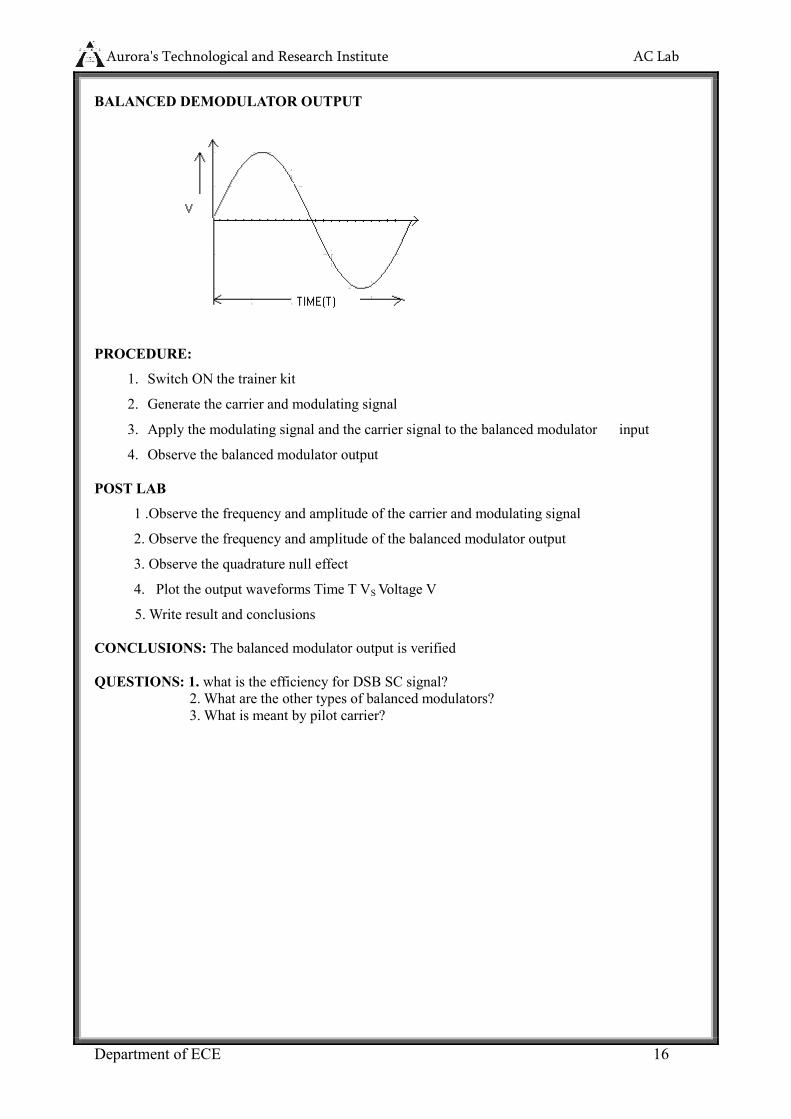
Auroras Technological and Research Institute AC Lab
Department of ECE 19
DSB-SC 0UTPUT
SSB-SC OUTPUT
PROCEDURE
a Modulation
1 Switch ON the trainer kit 2 Observe the output of RF generator using CROThere are two outputs from the RF
generator one is direct output and another is 90 deg phase shift with the direct output 3 Observe the output of AF generator using CROThere are two outputs from the AF
generator one is direct output and another is 90 deg phase shift with the direct output 4 Set the amplitude of the RF signal to 01vpp and connect the 0 deg phase shift signal to
one BM and 90 deg angle phase shift signal to the second BM
5 Set the AF Signal amplitude to 8vpp and connect to the BM 6 Observe the outputs of both balanced modulators simultaneously and adjust the balance
control until get the output waveforms (DSB SC) 7 To get LSB of SSB connect both balanced modulators outputs to SUBTRACTED circuit 8 Measure the frequencies of LSB using multimeter 9 Calculate the theoretical frequency of the SSB (LSB) and compare it with the practical
value LSB=RE Frequency ndashAF Frequency
10 To get USB of SSB signal connect both balanced modulators outputs to ADDER circuit 11 Measure the frequencies of USB
12 Calculate the theoretical value of the SSB Upper Side Band (SSB-USB) frequency and compare it with practical value
USB=RF Frequency+AF Frequency
Auroras Technological and Research Institute AC Lab
Department of ECE 20
b Demodulation (Synchronous detector)
1 Connect the SSB signal from the summer or sub tractor to the SSB signal input of the synchronous detector and RF signal (0ordm) to the RF input of the synchronous detector
2 Observe the Detector output using CRO and compare it with the AF signal (Modulating Signal)
3 Observe the SSB signal for the different frequencies of the AF signal (modulating signal)
TABULATION RF Frequency (Fc) =--------------------KHz
USB LSB
SNo AFsig
Freq(Fm) Practical Freq Theoretical
Freq=Fc+Fm
Practical Freq
Theoretical Freq=Fc-Fm
POST LAB
1 Observe the frequency and amplitude of the RF carrier both (900 amp 0 0 ) phase AF modulating signal (900 amp 0 0 ) phase DSB-SC SSB-SC LSB and USB of the SSB signal
2 Observe the frequency components and bandwidth of SSB
3 Plot the output waveforms above mentioned 4 Write result and conclusion
CONCLUSIONS Hence various outputs of SSB modulator are obtained
QUESTIONS 1 What are the advantages of SSB over AM
2 What is the main drawback of SSB
3 What is meant by VSB
Auroras Technological and Research Institute AC Lab
Department of ECE 21
EXPERIMENT NO 4
FREQUENCY MODULATION AND DEMODULATION
OBJECTIVE To study
1 Frequency modulation process
2 Measurement of Modulation Index
3 Measurement of Frequency deviation
4 Demodulation Process
PRE-LAB 1 Study the data sheet of IC LM 2206 LM 565
2 Study the theory of FM modulation and demodulation
3 Draw the circuit diagram for modulation and demodulation
4 Draw the expected wave forms
EQUIPMENT 1 Frequency modulation and demodulation trainer kit 1 No 2 Dual trace CRO 1 No 3 Connecting probe and cords
THEORY
In telecommunications frequency modulation (FM) conveys information over a carrier
wave by varying its frequency (contrast this with amplitude modulation in which the amplitude
of the carrier is varied while its frequency remains constant) In analog applications the
instantaneous frequency of the carrier is directly proportional to the instantaneous value of the
input signal Digital data can be sent by shifting the carriers frequency among a set of discrete
values a technique known as keying The instantaneous frequency of the oscillator and is the
frequency deviation which represents the maximum shift away from fc in one direction
assuming xm(t) is limited to the range plusmn1Although it may seem that this limits the frequencies in
use to fc plusmn fΔ this neglects the distinction between instantaneous frequency and spectral
frequency The frequency spectrum of an actual FM signal has components extending out to
infinite frequency although they become negligibly small beyond a point Carsons rule of
thumb Carsons rule states that nearly all (~98) of the power of a frequency-modulated signal
lies within a bandwidth
Auroras Technological and Research Institute AC Lab
Department of ECE 22
CIRCUIT DIAGRAM
MODULATION
DEMODULATION
Auroras Technological and Research Institute AC Lab
Department of ECE 23
OUT PUT WAVEFORMS
Auroras Technological and Research Institute AC Lab
Department of ECE 24
PROCEDURE a Modulation
i Switch ON the trainer kit ii Generate the carrier and modulating signal iii apply the modulating signal to the frequency modulator iv Trace the FM output
b Demodulation i apply the modulated FM output into Demodulation input ii Trace the demodulated output waveform
TABULATION
SNo
Amplitude of Modulating
Signal(Am) Fmin
Frequency
Deviation
∆f=fc-fmin or fc-fmax
Modulation Index β=∆ffm
POST LAB
1 Observe the frequency and amplitude of the carrier and modulating signal 2 Calculate the frequency deviation by observing Fmax and Fmin
δ=Fc-Fmax or δ=Fc-Fmin
3 Calculate modulation index β= δFm
4 Change the amplitude of the modulating signal and repeat steps 1 to 3 for different values of Am and note down the readings in table-1
5 Plot the output waveforms Time T VS Voltage Vo
6 Write result and conclusion
CONCLUSIONS Hence the frequency modulated output is obtained
QUESTIONS 1 what is meant by angle modulation
2 How FM is different from AM
3 What is meant by Carson Rule
4 What is the maximum modulation index
Auroras Technological and Research Institute AC Lab
Department of ECE 25
EXPERIMENT NO 5
STUDY OF SPECTRUM ANALIZER AND ANALYSIS OF AM amp FM SIGNALS
Auroras Technological and Research Institute AC Lab
Department of ECE 26
Auroras Technological and Research Institute AC Lab
Department of ECE 27
Auroras Technological and Research Institute AC Lab
Department of ECE 28
EXPERIMENT NO 6
PRE EMPHASIS AND DE EMPHASIS
OBJECTIVE To study the operation of Pre-emphasis and De-emphasis circuits
PRE-LAB
1 Study the theory of Pre-emphasis and De-emphasis circuits
2 Draw the circuit diagram
3 Draw the expected waveforms
COMPONENTS
1 Resistors 100kΩ 100Ω
2 Capacitors 1μf 100μf EQUIPMENT 1 Function generator 1
2 Dual trace CRO 1
THEORY Pre-emphasis
Improving the signal to noise ratio by increasing the magnitude of higher frequency
signals with respect to lower frequency signals
De-emphasis
Improving the signal to noise ratio by decreasing the magnitude of higher
frequency signals with respect to lower frequency signals
Transmitters that employ a true FM modulator require a pre emphasis circuit before the
modulator fore the true FM modulator doesnt automatically pre emphasize the audio like
a transmitter that uses a phase modulator A separate circuit is not necessary for pre
emphasis in a transmitter that has a phase modulator because the phase modulator applies
pre emphasis to the transmitted audio as a function of the phase modulator The receivers
De emphasis circuitry takes the unnatural sounding pre emphasized audio and turns it
back into its original response Pre emphasized (discriminator) audio is however available
directly from the audio demodulation (discriminator) circuitry In linking systems many
choose to eliminate the emphasis circuitry to allow better representation of retransmitted
Auroras Technological and Research Institute AC Lab
Department of ECE 29
signals Since the signal has already been pre emphasized (by the user that is
transmitting) and since the receiver you are listening to takes care of the de emphasis
CIRCUIT DIAGRAMS
PRE-EMPHASIS
DE-EMPHASIS
EXPECTED WAVEFORMS
INPUT
TIME T
A
m
p
l i t u
d
e
Am
Auroras Technological and Research Institute AC Lab
Department of ECE 30
OUTPUT
PRE-EMPHASIS
Freq Vs Gain
DE-EMPHASIS
Freq Vs Gain
TIME T
Freq f (Hz)
A
m
p
l i t u
d
e
Am
Auroras Technological and Research Institute AC Lab
Department of ECE 31
TABLE
PRE EMPHASIS
SNo Input Freq
Input Voltage Vi (Volts)
Output Voltage Vo (Volts) Gain=VoVi
Gain in dB
20log(voVi)
DE-EMPHASIS
SNo Input Freq
Input Voltage Vi (Volts)
Output Voltage Vo (Volts)
Gain=VoVi Gain in dB
20log(VoVi)
PROCEDURE a Pre-emphasis
1 Connect the circuit as per the circuit diagram
2 Apply a constant sine wave input across the input terminal of fixed amplitude(Vi) 3 By varying the input frequency note down the output amplitude (Vo) with respect to
input frequency in Table 4 Calculate the gain using the formula
5 Gain =20log (Vo) (Vi) db
b De-Emphasis
1 Connect the circuit as per the circuit diagram
2 Repeat the steps 2 3 amp4
POST LAB
1 Observe the output amplitude for both the pre-emphasis and De-emphasis circuits
2 Calculate the gain in db
3 Plot the frequency versus gain curves on logarithmic graphs for both the circuits
4 Plot the input and output waveforms Time T VS Voltage Vo
5 Write the result and conclusion
CONCLUSIONS Obtained the pre emphasis and de-emphasis outputs
QUESTIONS 1 Observe the out put signal is disturbed by noise what action has to be taken and measure the
output voltage 2 Where we use the pre emphasis circuit 3 Where we use the de emphasis circuit 4 What are the advantages of pre emphasis and de emphasis circuits
Auroras Technological and Research Institute AC Lab
Department of ECE 32
EXPERIMENT NO 7
TIME DIVISION MULTIPLEXING AND DEMULTIPLEXING
AIM To study Time Division Multiplexing and its waveforms
PRE LAB WORK
Study the operation of Time division multiplexer and demultiplexer Draw the block diagram of TDM
Draw the expected graphs of all necessary waveforms ( CH1CH2TDM OP and Demultiplexed OP)
EQUIPMENT
1) Experimental board on TDM
2) Dual Trace CRO 3) Probes
THEORY
Time Division Multiplexing (TDM) is a technique for transmitting serial messages on a signal
transmission channel by dividing the time division into slots One slot for each message The concept
of TDM comes from sampling theorem which enables use to transmit the information contained in the
band limited Signal using sampling of the signal taken uniformly or a rate slightly higher then the
Nyquist rate TDM enables the joint utilization at a common transmission channel by a number of
independent message sources without mutual interference
The different Ip message signals all band limited in WHz by the IP low pass filters and sequentially
sampled at the transmitters by a rotary switch or a comparator The switch makes are complete
revolution in Ts frac12 W extracting are sample from each IP The commutator OP is a PAM waveform
containing individual message sample
It there are N number of IP the pulse to Pulse spacing will be Ts = 1 while the spacing
N Nfs
bw successive samples from each IP is called a frame
At the receiver a similar rotatory switch the decommutator separates the samples and distributes them
to a bank of low-pass filters which in turn is usually electronic and synchronization signals are
provided to keep the distribute in step with the commutant
Auroras Technological and Research Institute AC Lab
Department of ECE 33
EXPECTED GRAPHS
PROCUDURE
1 Connect the OP of the experimental board to one of the channels on CRO 2 Switch ON the experimental board 3 Observe the OP waveforms 4 Vary the values of the resistors R1 R2 and R3 alternative and observe the OP on CRO
RESULT
The process of the Time Division Multiplexing and the waveforms has been studied
CONCLUSION
Auroras Technological and Research Institute AC Lab
Department of ECE 34
Figure 1 Time Division Multiplexing amp De multiplexing
Auroras Technological and Research Institute AC Lab
Department of ECE 35
EXPERIMENT NO 9
VERIFICATION OF SAMPLING THEOREM
AIM To study the effect of sampling on the transmission of information through PWM
PRE LAB WORK
Study the sampling theorem
Draw the expected graphs of all necessary waveforms ( message signal carrier wave PWM op demodulated op etc
EQUIPMENT
1) Experimental Board on study of sampling theorem 2) Dual trace CRO (0 ndash 20 MHz) 3) Function Generator 4) Connecting wires
THEORY
The principle of sampling can be explained using the switching sampler The switch periodically shifts below bw two constants at the rate of fs = 1 Ts Hz staying on the IP constant for each sampling period The op Xs(t) of the samples consists of segments of x(t) and Xc(t) can be represented as
Xs(t) = X(t) S(t)
Where S(t) is sampling or switching function There are a number of differences bw the ideal sampling and reconstruction techniques described in the proceeding sections of the actual signal
PROCEDURE
1) Observe the internal clock and measure its frequency and amplitude 2) Give the clock to the clock IP terminal 3) Connect the modulating signal to the IP 4) Check the condition fs gt 2fm and observe the de-modulated wave 5) Check the condition fs lt 2fm and fs = 2fm and draw the OP waveforms
RESULT
CONCLUSION
Aurorarsquos Technological and Research Institute DC Lab
36
Figure 2 Sampling Theorem
Aurorarsquos Technological and Research Institute DC Lab
37
EXPERIMENT NO 10
PULSE AMPLITUDE MODULATION AND DEMODULATION
AIM 1) To study the PAM modulation and its waveforms
2) To study the de-modular of PAM
3) To study the effect of sampling frequency on de-modulation OP
PRE LAB WORK
Study the operation Pulse Amplitude Modulator and Demodulator Draw the block diagram of PAM modulator and demodulator Draw the expected graphs of all necessary waveforms ( message signal carrier wave PAM op
demodulated op etc)
EQUIPMENT
1) Exp Board on study of PAM 2) CRO 3) Functional Generator 4) Connecting wires and chords
THEORY
In PAM the amplitude of the carrier wave of higher frequency follow the amp of the message signal
Within this (Modulation Sampling) we have two more types of sampling those are
(1) Natural Sampling
(2) Flat Top Sampling
Basically in Natural Sampling the carrier waves are train of pulses of a certain frequency After
sampling the top of the Pulse follow the message signal Due to this following of top of Pulses with the
message signals cause a distortion in De-modulation
In Flat top sampling also we use train of pulses for sampling but only the starting point of each pulse
follow the message signal remaining width of the pulse will (follow) be flat But here we go for Natural
sampling
EXPECTED WAVEFORMS
Aurorarsquos Technological and Research Institute DC Lab
38
PROCEDURE (MODULATION)
1 Observe the clock on CRO and measure its frequency and amp (freq 5KHz) 2 Connect the clock to clock IP terminals in modulation 3 Put control switch in ac position and set amplitude = OV This provides DC at Modulating
signal terminal 4 Connect the modulating signal or IP to the modulator 5 Connect one channel of CRO at lsquoTirsquo and Gnd Observe that the pulses are of same height
Height is adjustable by varying offset This is PAM signal with DC IP Measure amplitude and frequency of Pulses
6 Increase the amplitude of modulation signal Observe the amplitude and frequency of this sinusoidal modulating signal
7 Observe PAM signal
a) How many Pulses are there in one modulating cycle
b) It is natural or Flat Top PAM c) It is Single or dual polarity PAM
8 Observe the effect of DC offset on PAM waveform
DE-MODULATION
1) Generate undistorted PAM waveform 2) Connect the modulating signal to de-modulation IP 3) Observe the detected OP and measure its frequency which must be same as
modulating signal
EFFECT OF SAMPLING FREQUENCY
1) Connect internal sinusoidal signal to modulating signal IP of the modulator 2) Connect an external functional Generator at the circuit terminals of the modulator 3) Get the PAM waveform using the above circuit 4) Adjust the modulating amplitude offset and frequency to get an undistorted frequency 5) Connect the PAM to de-modulator IP 6) Observe the demodulated signal for various frequencies of clock (fs gt 2fm lt 2fm = 2 fm)
RESULT
CONCLUSION
Aurorarsquos Technological and Research Institute DC Lab
39
Figure 3 Pulse Amplitude Modulation
Auroras Technological and Research Institute AC Lab
Department of ECE 5
EXPERIMENT NO 11
PULSE WIDTH MODULATION AND DEMODULATION
AIM
1) To study the PWM process and the corresponding waveforms 2) To study the effect of sampling frequency on the transmission of information through PWM
PRE LAB WORK
Study the operation Pulse Width Modulator and Demodulator Draw the block diagram of PWM modulator and demodulator Draw the expected graphs of all necessary waveforms ( message signal carrier wave PWM op
demodulated op etc
EQUIPMENT
1) Experimental Board
2) Dual trace CRO 3) AF generator 4) Multimeter
THEORY
In PWM the samples of the message signal are used to vary the duration of the individual pulses The
pulse width may be varied by varying the time of occurrence of the leading edge trailing edge of both
edges of the pulse in accordance with the sampled value of the modulating wave PWM can also be
generated by using emitter follower monostable multivibrator is an excellent voltage to time converter
since its gate width is dependent on the voltage to which the capacitor is changed If this voltage can be
varied in accordance with a signal voltage a series of rectangular pulses can be obtained with width
varying as required
The demodulated of PWM is quite simple PWM is passed through a low pass filter The reconstruction is
associated with a certain amount of Distortion caused by the cross modulator products that fall in the
signal band
EXPECTED WAVEFORM
Aurorarsquos Technological and Research Institute DC Lab
41
PROCEDURE
STUDY OF MODULATION
1) Observe the clock on CRO and measure its frequency (fs) 2) Observe the sine wave modulating signal on CRO and observe the dc shift produced in this
by varying the offset nob Measure the frequency Variation limits of this signal 3) Apply clock at the circuit input terminal 4) Apply modulating signal by keeping the control switch in dc position 5) Observe the modulated wave 6) Plot the graph bw pulse width and the applied dc voltage 7) Put the control switch in sine wave position and adjust the modulating signal amplitude
frequency and dc offset to get the stationary waveform of PWM 8) Note the number of pulses in one circuit of modulating signal
STUDY OF DEMODULATION
1) Generate the stationary PWM waveform using sin wave modulating signal 2) Connect the modulator OP to PWM demodulator 3) Connect Channel (1) to Modulating Signal and channel (2) to demodulated wave
EFFECT OF SAMPLING FREQUENCY
1) Use an external square wave and connect it to the clock input 2) Set the frequency of square wave at frequency 2fm 3) Observe the demodulated wave
4) Change the frequency of square wave to fs lt 2fm fs gt 2fm and observe the demodulated wave
RESULT
CONCLUSION
Aurorarsquos Technological and Research Institute DC Lab
42
Figure 4 Pulse Width Modulation
Aurorarsquos Technological and Research Institute DC Lab
43
EXPERIMENT NO 12
PULSE POSITION MODULATION AND DEMODULATION
AIM
1) To study the PPM Modulation and the corresponding waveforms 2) To study the de-modulation of PPM 3) To see the effect of sampling frequency on the transmission of information through PPM
PRE LAB WORK
Study the operation Pulse Position Modulator and Demodulator Draw the block diagram of PPM modulator and demodulator Draw the expected graphs of all necessary waveforms ( message signal carrier wave PPM op
demodulated op etc
EQUIPMENT
1) Experimental Board for PPM
2) Dual Phase Oscilloscope
3) AF Generator
THEORY
In PDM long pulses expand considerable power duration If the pulse which bearing no additional
information If this un used power is subtracted from PDM so that only time transitions are preserved
We observe a more efficient type of pulse modulation known as pulse position modulation Here in the
Pulse Position Modulated wave the position of the Pulse relative to its unmodulated time of occurrence is
varied in accordance with the message signal
We generate a PPM wave from PWM wave by using a Monostable Multivibrator The device has one
absolutely stable state and one quest ndash stable state into which it is triggered by an externally applied Pulse
The monostable multivibrator is designed to trigger on the trailing edges of the duration ndash modulated pulse
is varied in accordance with the message signal
The fixed pulse duration of the PPM wave at the monostable multivibrator OP can be set by appropriately
choosing the resistance ndash capacitance combination in the timing circuit of the device
Aurorarsquos Technological and Research Institute DC Lab
44
EXPECTED WAVEFORM
PROCEDURE
STUDY OF MODULATION
Observe the clock and measure its frequency (fs) Apply the clock at the clock IP terminal in the modulator Apply the modulating signal keeping control switch in DC position Observe the PPM OP Connect the channel ndash (1) on CRO to clock and channel (2) to PPM wave OP Compare the position of two waveforms Vary the DC offset and observe the relative shift between the clock and PPM OP Measure the time shift between clock and PPM wave for various settings of offset Draw the graph between time shift and DC voltage Put the control switch in AC position adjusts the amplitude and frequency and offset
of sinusoidal modulating signal to get the stationary PPM wave Note the number of pulses in one cycle of the modulated wave
STUDY OF DEMODULATION
Generate a stationery PPM wave for a sinusoidal modulating signal Apply the PPM wave to the input of de-modulator Connect the Channel ndash (1) of CRO to the modulating signal and channel ndash 2 to the
de-modulator output Compare the two waveforms
Note the frequency of demodulated wave It should be same as the modulating signal Note down the waveform
RESULT
CONCLUSION
Aurorarsquos Technological and Research Institute DC Lab
45
Aurorarsquos Technological and Research Institute DC Lab
46
Figure 5 Pulse Position Modulation
Aurorarsquos Technological and Research Institute AC Lab
47
EXPERIMENT NO 13
FREQUENCY SYNTHESIZER
AIM
To study the operation of frequency synthesizer using PLL
PRE-LAB 1 Study the data sheet of IC 7404IC 4017IC 565 and IC 4046
2 Study the theory of frequency synthesizer 3 Draw the circuit diagram and expected waveforms
EQUIPMENTS
1 Frequency synthesizer trainer AET -26A
2 Dual trace CRO (20Mhz) 3 Digital frequency counter or multimeter
4 Patch chords
THEORY
A frequency synthesizer is an electronic system for generating any of a range
of frequencies from a single fixed time base or oscillator They are found in many modern
devices including radio receivers mobile telephones radiotelephones walkie-talkies CB
radios satellite receivers GPS systems etc A frequency synthesizer can combine
frequency multiplication frequency division and frequency mixing (the frequency mixing
process generates sum and difference frequencies) operations to produce the desired output
signal
BLOCK DIAGRAM
Phase Comparator
Amplifier Low pass filter
V C O
Div N Network frequency divider
Fin= fout
N
fin
Fout =Nf in
Aurorarsquos Technological and Research Institute AC Lab
48
SIMPLE 1KHZ-9KHZ FREQUENCY SYNTHESIZER
CIRCUIT DAIGRAM
PROCEDURE 1 Switch on the trainer ad verify the output of the regulated power supply ie 5V These
supplied are internally connected to the circuit so no extra connections are required 2 Observe output of the square wave generator using oscilloscope and measure the range
with the help of frequency counter frequency range should be around 1KHz to 10KHz 3 Calculate the free running frequency range of the circuit (VCO output between 4th pin
and ground 1 For different values of timing resistor R1 ( to measure Rt value using digital multimeter between given test points 1 And record the frequency values in table 1
Fout = 03 (RtCt) where Rt is the timing resistor and Ct is the timing capacitor = 001 f
Aurorarsquos Technological and Research Institute AC Lab
49
4 Connect 4th pin of LM 565 (Fout) to the driver stage and 5th pin (Phase comparator) connected to 11th pin of 7404 Output can be taken at the 11th pin of the 7490 It should be divided by the 2 amp 3 times of the fout
TABULATION
Fin KHz Fout = N x fin KHz Divided by 3 2
EXPECTED WAVEFORMS
POST LAB
1 Observe the synthesized output in table 2 Calculate the output frequency
3 Plot the output waveforms
4 Write result and conclusions
CONCLUSIONS
The various outputs of frequency synthesizer are verified
QUESTIONS
1 What are the applications of frequency synthesizer
TIME T
A
m
p
l i T
u
d
e
Ac
Aurorarsquos Technological and Research Institute AC Lab
50
2 What is the difference between heterodyning and synthesizer
Aurorarsquos Technological and Research Institute AC Lab
51
EXPERIMENT NO 14
AGC CHARATERISTICS
AIM
To observe the effect of automatic gain control(AGC)
PRE LAB 1 To study the theory of AGC 2 Draw the Block Diagram circuits diagram and expected waveforms
EQUIPMENTS 1 AGC Trainer Kit 2 CRO
3 Patch Chords
4 Digital Multimeter
THEORY
Automatic gain control (AGC) is an adaptive system found in many electronic
devices The average output signal level is fed back to adjust the gain to an appropriate level
for a range of input signal levels For example without AGC the sound emitted from an AM
radio receiver would vary to an extreme extent from a weak to a strong signal the AGC
effectively reduces the volume if the signal is strong and raises it when it is weaker AGC
algorithms often use a PID controller where the P term is driven by the error between
expected and actual output amplitude
Block Diagram
Frequency Converter
1st IF Amplifier
2nd IF Amplifier
Detector
Audio Preamplifier
Driver Output
Aurorarsquos Technological and Research Institute AC Lab
52
CIRCUIT DIAGRAM
PROCEDURE
1 Connect 455 KHz IF Signal Function Generator connect AGC link Connect CRO channel-1 at input terminals
2 Connect CRO channel 2 at collector of Q3 The amplified signal will be observed 3 Calculate the voltage gain by measuring the amplitude of output signal (Vo) waveform
using formula A=VoVi 4 Now connect CRO-2 channel at output The detected audio signal of 455 Khz will be
observed 5 Now vary input level of 455 KHz IF signal and observe detected 455 KHz audio signal
with and without AGC link The output will be distorted when AGC link is removed ie there is no AGC action
6 This explains AGC effect in Radio circuit
TABULATION
SNo Input Voltage Vi (P-P) With out AGC With AGC
Output Voltage Vo (P-P)
Gain A= Vo Vi
Output Voltage Vrsquoo (P-P)
Gain Arsquo= Vrsquoo Vi
Aurorarsquos Technological and Research Institute AC Lab
53
EXPECTED WAVEFORMS
AM Modulated RF Input
Detected Output with AGC
Detected Output without AGC
POST-LAB
1 Observe the input voltage and output voltage for with AGC and Without AGC in Table 1
2 Calculate Gain a=vovi for both cases 3 Plot the output waveforms Time T Vs Voltage Vo and input voltage Vi Vs Gain A 4 Write Result and Conclusions
CONCLUSIONS The AGC characteristics are verified
QUESTIONS 1 what is meant by AGC
2 What is the difference between simple AGC and delayed AGC
3 From which part of receiver AGC is obtained
TIME T
A
m
p
l i T
u
d
e
Ac
TIME T
A
m
p
l i T
u
d
e
Ac
TIME T
A
m
p
l i T
u
d
e
Ac
Aurorarsquos Technological and Research Institute AC Lab
54
EXPERIMENT NO 15
PHASE LOCKED LOOP
OBJECTIVE To study the Phase locked loop using 565 IC and to take input frequency given by an external signal source
PRE-LAB To Study
1 The data sheet of IC 565
2 The theory of Phase locked loop
3 About free running frequency locking range and capture range
4 Draw the circuit diagram and expected waveforms
EQUIPMENT 1 Function generator 2
2 Dual trace CRO 1
3 Phase locked loop trainer kit
THEORY
A phase-locked loop or phase lock loop (PLL) is a control system that generates a signal
that has a fixed relation to the phase of a reference signal A phase-locked loop circuit
responds to both the frequency and the phase of the input signals automatically raising or
lowering the frequency of a controlled oscillator until it is matched to the reference in both
frequency and phase A phase-locked loop is an example of a control system using negative
feedback Phase-locked loops are widely used in radio telecommunications computers and
other electronic applications They may generate stable frequencies recover a signal from a
noisy communication channel or distribute clock timing pulses in digital logic designs
such as microprocessors Since a single integrated circuit can provide a complete phase-
locked-loop building block the technique is widely used in modern electronic devices
with output frequencies from a fraction of a cycle per second up to many gigahertz
BLOCK DIAGRAM
Aurorarsquos Technological and Research Institute AC Lab
55
CIRCUIT DIAGRAM
PROCEDURE 1 Switch ON the trainer kit 2 Check the VCO output at pin 4 of IC 565 that is a square wave form The frequency of the
VCO Output depends on CT (001f) and RT (47kΩ) 3 Next short the pins 4amp5 and give signal of variable frequency and observe VCO output 4 Change the input frequency and observe the VCO output on the CRO 5 Between some frequencies the VCO output is locked to the input signal frequency This can
be observed by increasing or decreasing the frequency of the VCO output by changing input frequency
6 Before or after that frequency range the VCO output is not locked
7 Calculate Lock range (FL) and capture range (FC) by using the following formulas
FL = 8foVCO fo=03RtCT
FC=12π radic2πf236103 C2
Table1
SNo Locking Frequency Frequency Range From To
CHARTERISTICES
Aurorarsquos Technological and Research Institute AC Lab
56
CONCLUSIONS Obtained the lock range of PLL
QUESTIONS
1 Observe the VCO output when pins 4amp5 short and give square wave as signal 2 Define lock range and capture range
3 What are the basic applications of PLL
Aurorarsquos Technological and Research Institute AC Lab
57
ANNEXURE-I
EXPERIMENT NO 1
Aurorarsquos Technological and Research Institute AC Lab
58
CHARACTERISTICS OF MIXER
AIM
To study the functioning of a frequency mixer
PRE LAB 1 To study the theory of Mixer 2 Draw the circuit diagram and expected waveforms
EQUIPMENTS 1 Frequency mixer trainer kit 2 CRO (20MHz) 3 Connecting cords and probes 4 Function generator (1MHz)
THEORY
In receivers using the super heterodyne principle a signal at variable frequency is
converted to a fixed lower frequency IF before detection IF is called the intermediate frequency
In typical AM (Amplitude Modulation eg as used on medium wave) home receivers that
frequency is usually 455 kHz for FM VHF receivers it is usually 107 MHz An intermediate
frequency (IF) is a frequency to which a carrier frequency is shifted as an intermediate step in
transmission or reception Frequency modulation (FM) is a form of modulation that represents
information as variations in the instantaneous frequency of a carrier wave Very high frequency
(VHF) is the radio frequency range from 30 MHz (wavelength 10 m) to 300 MHz (wavelength 1
heterodyne receivers mix all of the incoming signals with an internally generated waveform
called the local oscillator The user tunes the radio by adjusting the sets oscillator frequency in
the mixer stage of a receiver the local oscillator signal multiplies with the incoming signals
which shifts them all down in frequency The one that shifts is passed on by tuned circuits
amplified and then demodulated to recover the original audio signal The oscillator also shifts a
copy of each incoming signal up in frequency by amount Those very high frequency images
are all rejected by the tuned circuits in the IF stage The Super heterodyne receiver (or to give it its
full name The Supersonic Heterodyne Receiver usually these days shortened to superhet) was
invented by Edwin Armstrong in 1918
Aurorarsquos Technological and Research Institute AC Lab
59
BLOCK DIAGRAM
CIRCUIT DIAGRAM
EXPECTED WAVEFORMS
INPUT SIGNAL Fx
INPUT SIGNAL Fy
TIME T
A
m
p
l i T
u
d
e
Ac
Aurorarsquos Technological and Research Institute AC Lab
60
MIXER OUTPUT(Fy-Fx)
PROCEDURE 1 Connect the circuit as per the given circuit diagram 2 Switch on the power supply of trainer kit 3 Apply a sine wave at input Fx of 2 VP-P amplitude and 100 KHz frequency 4 Apply a sine wave at input FY of 2 VP-P amplitude and 100 KHz frequency 5 Observe the output waveform on the CRO 6 Repeat the steps 34 and 5 by changing the values of Fx once greater than and less than
FY in a steps of 5Khz (in the range 80KHz to 120KHz)
TABULATION
TIME T
A
M
P
L
I T
U
D
E
TIME T
A
m
p
l i T
u
d
e
Ac
Aurorarsquos Technological and Research Institute AC Lab
61
SNo Freq (Fy)
(kHz) Amp(V) Freq(Fx) (kHz) Amp(V) Freq(Fy-Fx)
(kHz) Amp(V)
POST LAB 1 Observe the amplitude and time Of inputs and output in table
2 Draw the expected waveforms
3 Verify the output signal obtained with the theoretical value 4 Plot the graphs for Time T VS input signal (FX) Voltage V input signal (FY) Voltage V
and output Signal F(x-y) voltage V 5 Write result and conclusions
CONCLUSIONS
Obtained the output of the mixer for various inputs
QUESTIONS
1 what are the different types of mixtures available
2 What is meant by heterodyning
3 What is meant by IF
Aurorarsquos Technological and Research Institute AC Lab
62
EXPERIMENT NO 2
DIGITAL PHASE DETECTOR
OBJECTIVE To detect the phase difference between two square wave signals using digital phase detector
PRE LAB
1 To study the theory of digital phase detector and EX-OR gate operation and truth table 2 Draw the circuit diagram and expected output and input waveforms
EQUIPMENT 1 Digital phase detector trainer kit 2 Regulated power supplies
3 CRO (20MHz) 4 Connecting cords amp probes
5 Digital frequency counter or multimeter
THEORY
Phase detector is a frequency mixer or analog multiplier circuit that generates a voltage
signal which represents the difference in phase between two signal inputs It is an essential
element of the phase-locked loop (PLL)Detecting phase differences is very important in many
applications such as motor control radar and telecommunication systems servo mechanisms and
demodulators
Electronic phase detector
Some signal processing techniques such as those used in radar may require both the amplitude
and the phase of a signal to recover all the information encoded in that signal One technique is to
feed an amplitude-limited signal into one port of a product detector and a reference signal into the
other port the output of the detector will represent the phase difference between the signals If the
signal is different in frequency from the reference the detector output will be periodic at the
difference frequency Phase detectors for phase-locked loop circuits may be classified in two
types A Type I detector is designed to be driven by analog signals or square-wave digital signals
and produces an output pulse at the difference frequency The Type I detector always produces an
output waveform which must be filtered to control the phase-locked loop variable frequency
oscillator (VCO) A type II detector is sensitive only to the relative timing of the edges of the input
and reference pulses and produces a constant output proportional to phase difference when both
signals are at the same frequency This output will tend not to produce ripple in the control voltage
of the VCO
Aurorarsquos Technological and Research Institute AC Lab
63
BLOCK DIAGRAM OF PLL
CIRCUIT DIAGRAM
Aurorarsquos Technological and Research Institute AC Lab
64
EXPECTED WAVEFORMS
EX-OR PHASE DETECTOR
EDGE TRIGGERED OUTPUT
PROCEDURE
1 Switch on the trainer kit
2 Observe the output of the square wave generator available on the trainer kit using CRO
and measure the range with the help of frequency counter the frequency range should be
around 2 KHz to 13 KHz
3 Calculate the free running range of the VCO output ie between 4th pin of IC PLL 565
and ground For different values of timing resistor Rt fout is given by Fout =03 Rt Ct
where Ct timing capacitor = 001 μF Rt timing resistor
4 Connect the square wave to the input of IC PLL 565 and short 4th and 5th pin of PLL
Vary the input frequency of the square wave when the PLL is locked that is connected to
Aurorarsquos Technological and Research Institute AC Lab
65
one input fout EX-OR phase detector The other input fin of EX-OR phase detector is the
coming from inbuilt of square wave generator
5 Connect the pulse generator output to the input of IC 565 PLL and short 4th amp 5th pin of
PLL Vary the input frequency of the square wave when the PLL is locked that is
connected to one input of Edge triggered phase detector input ie fout The other input fin
of edge triggered phase detector is the pulse input coming from the inbuilt pulse generator
6 The dc output voltage of the exclusive-OR phase detector is a function of the phase
difference between its two inputs fin and fout
POST LAB
1 Observe the Voltage and Time of the two input square waves
2 Observe difference of two inputs as square wave output
3 Plot the inputs and output waveforms Time T VS Voltage V
CONCLUSIONS
The phase detector outputs are verified
QUESTIONS
1 What is the function of phase detector
2 What is the condition for getting maximum output
3 Advantages of digital phase detector over analog phase detector
Aurorarsquos Technological and Research Institute AC Lab
66
EXPERIMENT NO 3
COASTAS RECEIVER
AIM
To demodulate a DSB-SC signal using coastas receiver
PRE LAB 1 To study the operation of coastas receiver 2 Draw the circuit diagram and expected waveforms
EQUIPMENTS 1 Communications trainer kit 2 DSB-SC modulator trainer kit 3 CRO (20MHz) 4 Connecting cords and probes 5 Function generator (1MHz)
THEORY
This loop and its variations is much-used as a method of carrier acquisition (and
simultaneous message demodulation) in communication systems both analog and digital
It has the property of being able to derive a carrier from the received signal even when there is
no component at carrier frequency present in that signal (eg DSBSC) The requirement is that
the amplitude spectrum of the received signal be symmetrical about this frequency
The Costas loop is based on a pair of quadrature modulators - two multipliers
fed with carriers in phase-quadrature These multipliers are in the in-phase (I) and quadrature
phase (Q) arms of the arrangement Each of these multipliers is part of separate synchronous
demodulators The outputs of the modulators after filtering are multiplied together in a third
multiplier and the lowpass components in this product are used to adjust the phase of the local
carrier source - a VCO - with respect to the received signal The operation is such as to
maximise the output of the I arm and minimize that from the Q arm The output of the I arm
happens to be the message and so the Costas loop not only acquires the carrier but is a
(synchronous) demodulator as well A complete analysis of this loop is non-trivial It would
include the determination of conditions for stability and parameters such as lock range capture
range and so on
Aurorarsquos Technological and Research Institute AC Lab
67
BLOCK DIAGRAM
EXPECTED WAVEFORMS
DSB-SC modulated output
Aurorarsquos Technological and Research Institute AC Lab
68
Demodulated output of the coastas loop
PROCEDURE
1 Switch ON the DSB-SC trainer kit
2 Generate the carrier and modulating signal
3 Generate the DSB-SC modulated signal
4 Connect the required blocks of the coastas receiver in the communications kit
5 Apply the generated DSB-SC signal to the above connected coastas receiver
6 Observe that the output of the coastas receiver is the demodulated wave of DSB-SC signal
POST LAB
1 Observe the frequency and amplitude of the carrier and modulating signal
2 Observe the frequency and amplitude of the balanced modulator output
3 Observe the lock condition of the coastas loop
4 observe the output of the coastas demodulator
5 Write result and conclusions
CONCLUSIONS The balanced modulator output and the operation of coastas receiver is verified
QUESTIONS 1 what is the operation of coastas loop
2 What happens when the locking condition of the coastas loop occurs
3 Coastas loop can be used for demodulation of other modulation techniques also What are they
Aurorarsquos Technological and Research Institute AC Lab
69
MATLAB PROGRAMMES
Aurorarsquos Technological and Research Institute AC Lab
70
INDEX
1 Introduction - 70
2 Amplitude Modulation and Demodulation - 74
3 DSB-SC Modulation and Demodulation - 84
4 SSB-SC Modulation and Demodulation - 89
5 Frequency Modulation and Demodulation - 95
6 Phase Modulation and Demodulation - 99
7 Time Division Multiplexing and Demultiplexing - 100
8 Frequency Division Multiplexing and Demultiplexing- 103
9 Verification of Sampling Theorem - 104
10 Pulse Amplitude Modulation and Demodulation - 106
11 Pulse width Modulation and Demodulation - 108
12 Pulse Position Modulation and Demodulation - 110
13 PLL as FM Demodulator - 112
Aurorarsquos Technological and Research Institute AC Lab
71
1 INTRODUCTION
What Is Simulink
Simulink is a software package for modeling simulating and analyzing dynamic
systems It supports linear and nonlinear systems modeled in continuous time sampled time
or a hybrid of the two Systems can also be multirate ie have different parts that are
sampled or updated at different rates
Tool for Simulation
Simulink encourages you to try things out You can easily build models from scratch
or take an existing model and add to it You have instant access to all the analysis tools in
MATLABreg so you can take the results and analyze and visualize them A goal of Simulink
is to give you a sense of the fun of modeling and simulation through an environment that
encourages you to pose a question model it and see what happens
Simulink is also practical With thousands of engineers around the world using it to
model and solve real problems knowledge of this tool will serve you well throughout your
professional career
Tool for Model-Based Design
With Simulink you can move beyond idealized linear models to explore more realistic
nonlinear models factoring in friction air resistance gear slippage hard stops and the other
things that describe real-world phenomena Simulink turns your computer into a lab for
modeling and analyzing systems that simply wouldnt be possible or practical otherwise
whether the behavior of an automotive clutch system the flutter of an airplane wing the
dynamics of a predator-prey model or the effect of the monetary supply on the economy
For modeling Simulink provides a graphical user interface (GUI) for building models
as block diagrams using click-and-drag mouse operations With this interface you can draw
the models just as you would with pencil and paper (or as most textbooks depict them) This
is a far cry from previous simulation packages that require you to formulate differential
equations and difference equations in a language or program Simulink includes a
comprehensive block library of sinks sources linear and nonlinear components and
connectors You can also customize and create your own blocks For information on creating
your own blocks see the separate Writing S-Functions guide
Models are hierarchical so you can build models using both top-down and bottom-up
approaches You can view the system at a high level then double-click blocks to go down
through the levels to see increasing levels of model detail This approach provides insight into
how a model is organized and how its parts interact
After you define a model you can simulate it using a choice of integration methods either
from the Simulink menus or by entering commands in the MATLAB Command Window The
menus are particularly convenient for interactive work while the command-line approach is
very useful for running a batch of simulations (for example if you are doing Monte Carlo
simulations or want to sweep a parameter across a range of values) Using scopes and other
display blocks you can see the simulation results while the simulation is running In addition
Aurorarsquos Technological and Research Institute AC Lab
72
you can change many parameters and see what happens for what if exploration The
simulation results can be put in the MATLAB workspace for post processing and
visualization
Model analysis tools include linearization and trimming tools which can be accessed
from the MATLAB command line plus the many tools in MATLAB and its application
toolboxes And because MATLAB and Simulink are integrated you can simulate analyze
and revise your models in either environment at any point
1 Generation of cosine wave in time domain and frequency
domain Clc clear all close all x = -500015 t = 0140001 time = cos(23141000t) y1 = cos(23141000x) subplot(211) plot(xy1) axis([-5 5 -3 3]) grid on title(Time domain) xlabel(Time ) ylabel(Amplitude) now create a frequency vector for the x-axis and plot the magnitude and phase subplot(212) fre = abs(fft(time)) f = (0length(fre) - 1)4000length(fre) plot(ffre) grid on title(Frequency domain (Spectrum)) xlabel(Freq ) ylabel(Amplitude)
WAVEFORMS
Aurorarsquos Technological and Research Institute AC Lab
73
2 Generation of square wave in time domain and frequency
domain
clc clear all close all x = -500015 Fs = 399 t = 01Fs1 time = SQUARE(2pi1000t) y1 = SQUARE(23141000x) subplot(211) plot(xy1) axis([-5 5 -3 3]) grid on xlabel(Time domain) ylabel(Amplitude) now create a frequency vector for the x-axis and plot the magnitude and phase subplot(212) fre = abs(fft(time)) f = (0length(fre) - 1)Fslength(fre) plot(ffre) grid on xlabel(Freq domain) ylabel(Amplitude)
WAVEFORMS
Aurorarsquos Technological and Research Institute AC Lab
74
Aurorarsquos Technological and Research Institute AC Lab
75
2 AMPLITUDE MODULATION AND DEMODULATION PROGRAM 1
clc clear all close all Ac=1 Carrier Amplitude Fc=04 Carrier frequency Fm=005 baseband frequency Fs=10 sampling t=001200 mt=cos(2piFmt) under modulation mu=05 st=Ac(1+mumt)cos(2piFct) subplot(211) plot(tst) hold on plot(tAc(mumt+ones(1length(mt)))r) plot(t-Ac(mumt+ones(1length(mt)))r) hold off title(Modulation Index = 05 under modulation Ac(1+05cos(2pi005t))cos(2pi04t)) xlabel(time (s))ylabel(amplitude) st_fft=fft(st) st_fft=fftshift(st_fft) st_fft_fre=5linspace(-11length(st_fft)) subplot(212) plot(st_fft_freabs(st_fft)) title(spectrum with Modulation Index = 05) xlabel(Frequency (Hz))axis([-1 1 0 1000Ac+100])
total modulation figure mu=1 st=Ac(1+mumt)cos(2piFct) subplot(211) plot(tst) hold on plot(tAc(mumt+ones(1length(mt)))r) plot(t-Ac(mumt+ones(1length(mt)))r) hold off title(Modulation Index = 1 modulation Ac(1+1cos(2pi005t))cos(2pi04t)) xlabel(time (s))ylabel(amplitude) st_fft=fft(st) st_fft=fftshift(st_fft) st_fft_fre=Fs2linspace(-11length(st_fft)) subplot(212) plot(st_fft_freabs(st_fft)) title(spectrum with Modulation Index = 1) xlabel(Frequency (Hz))axis([-1 1 0 1000Ac+100])
Aurorarsquos Technological and Research Institute AC Lab
76
over Modulation figure mu=2 st=Ac(1+mumt)cos(2piFct) subplot(211) plot(tst) hold on plot(tAc(mumt+ones(1length(mt)))r) plot(t-Ac(mumt+ones(1length(mt)))r) hold offtitle(Modulation Index = 2 over modulation Ac(1+2cos(2pi005t))cos(2pi04t)) xlabel(time (s))ylabel(amplitude) st_fft=fft(st) st_fft=fftshift(st_fft) st_fft_fre=Fs2linspace(-11length(st_fft)) subplot(212) plot(st_fft_freabs(st_fft)) title(spectrum with Modulation Index = 2) xlabel(Frequency (Hz))axis([-1 1 0 1000Ac+100])
WAVEFORMS
Aurorarsquos Technological and Research Institute AC Lab
77
PROGRAM 2
Aurorarsquos Technological and Research Institute AC Lab
78
task 1 fc=154000
task 2 fm=fc10 fs=100fc t=01fs4fm xc=cos(2pifct) xm=cos(2pifmt) figure(1) subplot(211)plot(txc) title(carrier signal of 154 khz) xlabel(time (sec)) ylabel(amplitude) subplot(212)plot(txm) title(message signal of 154 khz) xlabel(time (sec)) ylabel(amplitude) DSB-SC MODULATION mu = input( enter the Modulation Index value ) z1=(1+muxm)xc figure(2)
task 31 subplot(211)plot(tz1) title(AMPLITUDE MODULATION IN TIME DAOMAIN) xlabel(time (sec)) ylabel(amplitude)
task 32 l1=length(z1) f=linspace(-fs2fs2l1) Z1=fftshift(fft(z1l1)l1) subplot(212)plot(fabs(Z1)) title(AMPLITUDE MODULATION IN FREQUENCY DOMAIN) xlabel(frequency(hz)) ylabel(amplitude) axis([-200000 200000 0 03])
task 33 demodulation s1=z1xc S1=fftshift(fft(s1length(s1))length(s1)) figure(3) plot(fabs(S1)) title( demodulated signal IN FREQUENCY DOMAIN before filtring) xlabel(frequency(hz)) ylabel(amplitude) axis([-200000 200000 0 03]) hold on Hlp=1sqrt(1+(ffc)^(2100)) plot(fHlpr) title( frequency response of low pass filter) xlabel(frequency(hz)) ylabel(amplitude) axis([-200000 200000 0 2])
task 34 E1=HlpS1 figure(4) subplot(211)plot(fE1)
Aurorarsquos Technological and Research Institute AC Lab
79
title( Recover signal IN FREQUENCY DOMAIN after filtring) xlabel(frequency(hz)) ylabel(amplitude) axis([-200000 200000 0 03]) e1=ifft(ifftshift(E1))length(E1) subplot(212)plot(t(105)e1) title( Recover signal IN Time DOMAIN after filtring) xlabel(time(sec)) ylabel(amplitude)
WAVEFORMS
enter the Modulation Index value 05
0 1 2 3
x 10-4
-1
-05
0
05
1carrier signal of 154 khz
time (sec)
am
plit
ude
0 1 2 3
x 10-4
-1
-05
0
05
1message signal of 154 khz
time (sec)
am
plit
ude
Aurorarsquos Technological and Research Institute AC Lab
80
0 1 2 3
x 10-4
-2
-1
0
1
2AMPLITUDE MODULATION IN TIME DAOMAIN
time (sec)
am
plit
ude
-2 -15 -1 -05 0 05 1 15 2
x 105
0
01
02
AMPLITUDE MODULATION IN FREQUENCY DOMAIN
frequency(hz)
am
plit
ude
-2 -15 -1 -05 0 05 1 15 2
x 105
0
02
04
06
08
1
12
14
16
18
2 frequency response of low pass filter
frequency(hz)
am
plit
ude
Aurorarsquos Technological and Research Institute AC Lab
81
enter the Modulation Index value 1
-2 -15 -1 -05 0 05 1 15 2
x 105
0
01
02
Recover signal IN FREQUENCY DOMAIN after filtring
frequency(hz)
am
plit
ude
0 1 2 3
x 10-4
05
1
15
2 Recover signal IN Time DOMAIN after filtring
time(sec)
am
plit
ude
0 1 2 3
x 10-4
-2
-1
0
1
2AMPLITUDE MODULATION IN TIME DAOMAIN
time (sec)
am
plit
ude
-2 -15 -1 -05 0 05 1 15 2
x 105
0
01
02
AMPLITUDE MODULATION IN FREQUENCY DOMAIN
frequency(hz)
am
plit
ude
Aurorarsquos Technological and Research Institute AC Lab
82
enter the Modulation Index value 2
-2 -15 -1 -05 0 05 1 15 2
x 105
0
02
04
06
08
1
12
14
16
18
2 frequency response of low pass filter
frequency(hz)
am
plit
ude
-2 -15 -1 -05 0 05 1 15 2
x 105
0
01
02
Recover signal IN FREQUENCY DOMAIN after filtring
frequency(hz)
am
plit
ude
0 1 2 3
x 10-4
0
1
2
3 Recover signal IN Time DOMAIN after filtring
time(sec)
am
plit
ude
Aurorarsquos Technological and Research Institute AC Lab
83
0 1 2 3
x 10-4
-4
-2
0
2
4AMPLITUDE MODULATION IN TIME DAOMAIN
time (sec)
am
plit
ude
-2 -15 -1 -05 0 05 1 15 2
x 105
0
01
02
AMPLITUDE MODULATION IN FREQUENCY DOMAIN
frequency(hz)
am
plit
ude
-2 -15 -1 -05 0 05 1 15 2
x 105
0
02
04
06
08
1
12
14
16
18
2 frequency response of low pass filter
frequency(hz)
am
plit
ude
Aurorarsquos Technological and Research Institute AC Lab
84
-2 -15 -1 -05 0 05 1 15 2
x 105
0
01
02
Recover signal IN FREQUENCY DOMAIN after filtring
frequency(hz)
am
plit
ude
0 1 2 3
x 10-4
-2
0
2
4 Recover signal IN Time DOMAIN after filtring
time(sec)
am
plit
ude
Aurorarsquos Technological and Research Institute AC Lab
85
3 DOUBLE SIDEBAND ndash SUPRESSED CARRIER MODULATION
AND DEMODULATION
PROGRAM 1 clc clear all close all Ts = 199 subplot(411) t = 01Ts1 m = cos(2pi1000t) plot(tm) title(Modulating Signal ) xlabel(Time) ylabel(Amplitude) grid on plot of the carrier signal
subplot(412) c = cos(2pi5000t) plot(tc) title(Carrier Signal ) xlabel(Time) ylabel(Amplitude) grid on plot of the DSB signal with Suppresed carrier intime domain
subplot(413) d = mc plot(td) title(DOUBLE SIDEBAND ndash SUPRESSED CARRIER SIGNAL ) xlabel(Time) ylabel(Amplitude) grid on freq domain of the DSB signal
subplot(414) fre = abs(fft(d)) f = (0length(fre) - 1)Tslength(fre) plot(ffre) axis([0 100 0 50]) grid on title(DOUBLE SIDEBAND ndash SUPRESSED CARRIER SPECTRUM ) xlabel(Freq domain) ylabel(Amplitude)
Aurorarsquos Technological and Research Institute AC Lab
86
WAVEFORMS
0 01 02 03 04 05 06 07 08 09 1-1
0
1Modulating Signal
Time
Am
plit
ude
0 01 02 03 04 05 06 07 08 09 1-1
0
1Carrier Signal
Time
Am
plit
ude
0 01 02 03 04 05 06 07 08 09 1-1
0
1DOUBLE SIDEBAND ndash SUPRESSED CARRIER SIGNAL
Time
Am
plit
ude
0 10 20 30 40 50 60 70 80 90 1000
50DOUBLE SIDEBAND ndash SUPRESSED CARRIER SPECTRUM
Freq domain
Am
plit
ude
Aurorarsquos Technological and Research Institute AC Lab
87
PROGRAM 2 task 1 fc=154000 task 2 fm=fc10 fs=100fc t=01fs4fm xc=cos(2pifct) xm=cos(2pifmt) figure(1) subplot(211)plot(txc) title(carrier signal of 154 khz) xlabel(time (sec)) ylabel(amplitude) subplot(212)plot(txm) title(message signal of 154 khz) xlabel(time (sec)) ylabel(amplitude) DSB-SC MODULATION z1= xmxc figure(2) task 31 subplot(211)plot(tz1) title(DSB-SC MODULATION IN TIME DAOMAIN) xlabel(time (sec)) ylabel(amplitude) task 32 l1=length(z1) f=linspace(-fs2fs2l1) Z1=fftshift(fft(z1l1)l1) subplot(212)plot(fabs(Z1)) title(DSB SC MODULATION IN FREQUENCY DOMAIN) xlabel(frequency(hz)) ylabel(amplitude) axis([-200000 200000 0 03]) task 33 demodulation s1=z1xc S1=fftshift(fft(s1length(s1))length(s1)) figure(3) plot(fabs(S1)) title( demodulated signal IN FREQUENCY DOMAIN before filtring) xlabel(frequency(hz)) ylabel(amplitude) axis([-200000 200000 0 03]) hold on Hlp=1sqrt(1+(ffc)^(2100)) plot(fHlpg) title( frequency response of low pass filter) xlabel(frequency(hz)) ylabel(amplitude) axis([-200000 200000 0 2]) task 34 E1=HlpS1 figure(4) subplot(211)plot(fE1) title( Recover signal IN FREQUENCY DOMAIN after filtring) xlabel(frequency(hz)) ylabel(amplitude) axis([-200000 200000 0 03]) e1=ifft(ifftshift(E1))length(E1) subplot(212)plot(t(105)e1)
Aurorarsquos Technological and Research Institute AC Lab
88
title( Recover signal IN Time DOMAIN after filtring) xlabel(time(sec)) ylabel(amplitude) WAVEFORMS
0 1 2 3
x 10-4
-1
-05
0
05
1carrier signal of 154 khz
time (sec)
ampl
itude
0 1 2 3
x 10-4
-1
-05
0
05
1message signal of 154 khz
time (sec)
ampl
itude
0 1 2 3
x 10-4
-1
-05
0
05
1DSB-SC MODULATION IN TIME DAOMAIN
time (sec)
ampl
itude
-2 -15 -1 -05 0 05 1 15 2
x 105
0
01
02
DSB SC MODULATION IN FREQUENCY DOMAIN
frequency(hz)
ampl
itude
Aurorarsquos Technological and Research Institute AC Lab
89
-2 -15 -1 -05 0 05 1 15 2
x 105
0
02
04
06
08
1
12
14
16
18
2 frequency response of low pass filter
frequency(hz)
ampl
itude
-2 -15 -1 -05 0 05 1 15 2
x 105
0
01
02
Recover signal IN FREQUENCY DOMAIN after filtring
frequency(hz)
am
plit
ude
0 1 2 3
x 10-4
-1
0
1
2 Recover signal IN Time DOMAIN after filtring
time(sec)
am
plit
ude
Aurorarsquos Technological and Research Institute AC Lab
90
4 SINGLE SIDE BAND - SUPRESSED CARRIER MODULATION AND DEMODULATION
PROGRAM 1
clc clear all close all Ts = 199 subplot(411) t = 01Ts1 xm = cos(2pi1000t) plot(txm) title(Modulating Signal ) xlabel(Time) ylabel(Amplitude) grid on plot of the carrier signal subplot(412) c = cos(2pi5000t) plot(tc) title(Carrier Signal ) xlabel(Time) ylabel(Amplitude) grid on subplot(413) helbert transform of messeage signal xh=cos((2pi1000t)-pi2) SSB UPPER SIDE BAND MODULATION d= (xmcos(2pi5000t))-(xhsin(2pi5000t)) plot(td) title(SINGLE SIDEBAND ndash SUPRESSED CARRIER SIGNAL ) xlabel(Time) ylabel(Amplitude) grid on freq domain of the DSB signal subplot(414) fre = abs(fft(d)) f = (0length(fre) - 1)Tslength(fre) plot(ffre) axis([0 100 0 50]) grid on title(SINGLE SIDEBAND ndash SUPRESSED CARRIER SPECTRUM ) xlabel(Freq domain) ylabel(Amplitude)
Aurorarsquos Technological and Research Institute AC Lab
91
WAVEFORMS
0 01 02 03 04 05 06 07 08 09 1-1
0
1Modulating Signal
Time
Am
plit
ude
0 01 02 03 04 05 06 07 08 09 1-1
0
1Carrier Signal
Time
Am
plit
ude
0 01 02 03 04 05 06 07 08 09 1-1
0
1SINGLE SIDEBAND ndash SUPRESSED CARRIER SIGNAL
Time
Am
plit
ude
0 10 20 30 40 50 60 70 80 90 1000
50SINGLE SIDEBAND ndash SUPRESSED CARRIER SPECTRUM
Freq domain
Am
plit
ude
Aurorarsquos Technological and Research Institute AC Lab
92
PROGRAM 2
task 1 fc=154000
task 2 fm=fc10 fs=100fc t=01fs4fm xc=cos(2pifct) xm=cos(2pifmt)
task 41 xh=cos((2pifmt)-pi2) helbert transform which is the phase shift of pi2 in messeage signal SSB UPPER SIDE BAND MODULATION z2= (xmcos(2pifct))-(xhsin(2pifct)) figure(5) subplot(211)plot(tz2) title(SSB USB MODULATION IN TIME DAOMAIN) xlabel(time (sec)) ylabel(amplitude) l2=length(z2) f=linspace(-fs2fs2l2) Z1=fftshift(fft(z2l2)l2) subplot(212)plot(fabs(Z1)) title(SSB USB MODULATION IN FREQUENCY DOMAIN) xlabel(frequency(hz)) ylabel(amplitude) axis([-400000 400000 0 1]) apply local carrier for demodulation z1= z2xc figure(6)
task 42 subplot(211)plot(tz1) title(DEMODULATED SSB in time domain) xlabel(time (sec)) ylabel(amplitude) l1=length(z1) f=linspace(-fs2fs2l1) Z1=fftshift(fft(z1l1)l1) subplot(212)plot(fabs(Z1)) title(DEMODULATED SSB IN FREQUENCY DOMIAN) xlabel(frequency(hz)) ylabel(amplitude) axis([-400000 400000 0 03])
task 43 figure(7) plot(fabs(Z1)) title(FILTERING SIGNAL) xlabel(frequency(hz)) ylabel(amplitude) hold on Hlp=1sqrt(1+(ffc)^(2100)) plot(fHlpg) title( frequency response of low pass filter) xlabel(frequency(hz)) ylabel(amplitude)
Aurorarsquos Technological and Research Institute AC Lab
93
axis([-400000 400000 0 2])
task 44 E1=HlpZ1 figure(8) subplot(211)plot(fE1) title( Recover signal IN FREQUENCY DOMAIN after filtring) xlabel(frequency(hz)) ylabel(amplitude) axis([-400000 400000 0 03]) e1=ifft(ifftshift(E1))length(E1) subplot(212)plot(t(105)e1) title( Recover signal IN Time DOMAIN after filtring) xlabel(time(sec)) ylabel(amplitude)
WAVEFORMS
0 1 2 3
x 10-4
-1
-05
0
05
1SSB USB MODULATION IN TIME DAOMAIN
time (sec)
am
plit
ude
-4 -3 -2 -1 0 1 2 3 4
x 105
0
05
1SSB USB MODULATION IN FREQUENCY DOMAIN
frequency(hz)
am
plit
ude
Aurorarsquos Technological and Research Institute AC Lab
94
0 1 2 3
x 10-4
-1
-05
0
05
1DEMODULATED SSB in time domain
time (sec)
am
plit
ude
-4 -3 -2 -1 0 1 2 3 4
x 105
0
01
02
DEMODULATED SSB IN FREQUENCY DOMIAN
frequency(hz)
am
plit
ude
-4 -3 -2 -1 0 1 2 3 4
x 105
0
02
04
06
08
1
12
14
16
18
2 frequency response of low pass filter
frequency(hz)
am
plit
ude
Aurorarsquos Technological and Research Institute AC Lab
95
-4 -3 -2 -1 0 1 2 3 4
x 105
0
01
02
Recover signal IN FREQUENCY DOMAIN after filtring
frequency(hz)
am
plit
ude
0 1 2 3
x 10-4
-1
0
1
2 Recover signal IN Time DOMAIN after filtring
time(sec)
am
plit
ude
Aurorarsquos Technological and Research Institute AC Lab
96
5 FREQUENCY MODULATION AND DEMODULATION
clc clear all close all Frequency MODULATION of Triangular Signal t = -0041e-4004 Ta = 001 fc = 200 Frequency of carrier msg = msg1(tTa) Calling Function to Generate Msg Signal MODULATION kf = 160pi m_int = kf1e-4cumsum(msg) Integrating Msg fm = cos(2fcpit + m_int) fm = cos(2pifct + integral(msg)) DEMODULATION (Using Differentiator) dem = diff(fm) dem = [0dem] rect_dem = abs(dem) Filtering out High Frequencies N = 80 Order of Filter Wn = 1e-2 Pass Band Edge Frequency a = fir1(NWn) Return Numerator of Low Pass FIR filter b = 1 Denominator of Low Pass FIR Filter rec = filter(abrect_dem) Finding frequency Response of Signals fl = length(t) fl = 2^ceil(log2(fl)) f = (-fl2fl2-1)(fl1e-4) mF = fftshift(fft(msgfl)) Frequency Response of Message Signal fmF = fftshift(fft(fmfl)) Frequency Response of FM Signal Frequency Response of Rectified FM Signal rect_demF = fftshift(fft(rect_demfl)) Frequency Response of Recovered Message Signal recF = fftshift(fft(recfl)) Plotting signal in time domain figure subplot(211) plot(tmsg) title(Message Signal) xlabel(it t (sec)) ylabel(Amplitude)) grid subplot(212) plot(tfm)
Aurorarsquos Technological and Research Institute AC Lab
97
title(FM) xlabel(it t (sec)) ylabel(Amplitude) grid figure subplot(211) plot(trect_dem) title(Rectified FM) xlabel(it t (sec)) ylabel(Amplitude) grid subplot(212) plot(trec) title(Recovered Signal) xlabel(it t (sec)) ylabel(Amplitude) grid Plotting Freq Response of Signals figure subplot(221) plot(fabs(mF)) title(Freq Response of MSG) xlabel(f(Hz)) ylabel(Amplitude) grid axis([-600 600 0 200]) subplot(222) plot(fabs(fmF)) title(Freq Response of FM) grid xlabel(f(Hz)) ylabel(Amplitude) axis([-600 600 0 300]) subplot(223) plot(fabs(rect_demF)) title(Freq Response of Rectified FM) xlabel(f(Hz)) ylabel(Amplitude) grid axis([-600 600 0 100]) subplot(224) plot(fabs(recF)) title(Freq Response of Recovered Signal) xlabel(f(Hz)) ylabel(Amplitude) grid axis([-600 600 0 100])
Function to give message signal
Function of Msg(tri) function a = msg1(tTa) t1 = -0021e-40
Aurorarsquos Technological and Research Institute AC Lab
98
t2 = 01e-4002 m1 = 1 - abs((t1+Ta)Ta) m1 = [zeros([1 200])m1zeros([1 400])] m2 = 1 - abs((t2-Ta)Ta) m2 = [zeros([1 400])m2zeros([1 200])] a = m1 - m2 end
WAVEFORMS
-004 -003 -002 -001 0 001 002 003 004-1
-05
0
05
1Message Signal
t (sec)
Am
plit
ude)
-004 -003 -002 -001 0 001 002 003 004-1
-05
0
05
1FM
t (sec)
Am
plit
ude
Aurorarsquos Technological and Research Institute AC Lab
99
-004 -003 -002 -001 0 001 002 003 0040
005
01
015
02Rectified FM
t (sec)
Am
plit
ude
-004 -003 -002 -001 0 001 002 003 0040
005
01
015
02Recovered Signal
t (sec)
Am
plit
ude
-500 0 5000
50
100
150
200Freq Response of MSG
f(Hz)
Am
plit
ude
-500 0 5000
100
200
300Freq Response of FM
f(Hz)
Am
plit
ude
-500 0 5000
50
100Freq Response of Rectified FM
f(Hz)
Am
plit
ude
-500 0 5000
50
100Freq Response of Recovered Signal
f(Hz)
Am
plit
ude
Aurorarsquos Technological and Research Institute AC Lab
100
6 PHASE MODULATION AND DEMODULATION
clear all close all t = 00011 time variable fc = 5 carrier frequency ------------------------------------------ create message signal m(t) m = sin(2pit) ------------------------------------------ kp = pi2 phase deviation constant ------------------------------------------------ modulating the carrier with the message signal carrier = cos(2pifct) modulated = cos(2pifct + kpm) ------------------------------------------------ ------------------------------------------------ Plotting the signals plot(tmbtcarrierrtmodulatedk--) axis([0 1 -15 15]) xlabel(Time(seconds)) ylabel(Amplitude(volt)) title(Phase modulation) legend(MessageCarrierModulated)
WAVEFORMS
0 01 02 03 04 05 06 07 08 09 1-15
-1
-05
0
05
1
15
Time(seconds)
Am
plit
ude(v
olt)
Phase modulation
Message
Carrier
Modulated
Aurorarsquos Technological and Research Institute AC Lab
101
7 TIME DIVISION MULTIPLEXING AND DEMULTIPLEXING clc close all clear all Signal generation x=058pi sig1=8sin(x-pi) generate 1st sinusoidal signal l=length(sig1) sig2=8square(x) Generate 2nd traingular Sigal Display of Both Signal subplot(221) plot(sig1) title(Sinusoidal Signal) ylabel(Amplitude---gt) xlabel(Time---gt) subplot(222) plot(sig2) title(Triangular Signal) ylabel(Amplitude---gt) xlabel(Time---gt) Display of Both Sampled Signal subplot(223) stem(sig1) title(Sampled Sinusoidal Signal) ylabel(Amplitude---gt) xlabel(Time---gt) subplot(224) stem(sig2) title(Sampled Triangular Signal) ylabel(Amplitude---gt) xlabel(Time---gt) l1=length(sig1) l2=length(sig2) for i=1l1 sig(1i)=sig1(i) sig(2i)=sig2(i) end TDM of both quantize signal tdmsig=reshape(sig12l1) Display of TDM Signal figure stem(tdmsig) title(TDM Signal) ylabel(Amplitude---gt) xlabel(Time---gt) Demultiplexing of TDM Signal demux=reshape(tdmsig2l1) for i=1l1 sig3(i)=demux(1i) sig4(i)=demux(2i) end
display of demultiplexed signal figure subplot(211)
Aurorarsquos Technological and Research Institute AC Lab
102
plot(sig3) title(Recovered Sinusoidal Signal) ylabel(Amplitude---gt) xlabel(Time---gt) subplot(212) plot(sig4) title(Recovered Triangular Signal) ylabel(Amplitude---gt) xlabel(Time---gt)
WAVEFORMS
0 20 40 60-10
-5
0
5
10Sinusoidal Signal
Am
plit
ude--
-gt
Time---gt
0 20 40 60-10
-5
0
5
10Square Signal
Am
plit
ude--
-gt
Time---gt
0 20 40 60-10
-5
0
5
10Sampled Sinusoidal Signal
Am
plit
ude--
-gt
Time---gt
0 20 40 60-10
-5
0
5
10Sampled Square Signal
Am
plit
ude--
-gt
Time---gt
Aurorarsquos Technological and Research Institute AC Lab
103
0 20 40 60 80 100 120-8
-6
-4
-2
0
2
4
6
8TDM Signal
Am
plit
ude--
-gt
Time---gt
0 10 20 30 40 50 60-10
-5
0
5
10Recovered Sinusoidal Signal
Am
plit
ude--
-gt
Time---gt
0 10 20 30 40 50 60-10
-5
0
5
10Recovered Square Signal
Am
plit
ude--
-gt
Time---gt
Aurorarsquos Technological and Research Institute AC Lab
104
8 FREQUENCY DIVISION MULTIPLEXING AND
DEMULTIPLEXING
Aurorarsquos Technological and Research Institute AC Lab
105
9 VERIFICATION OF SAMPLING THEOREM [
clear all close all clc Fs = input(Enter Sampling Frequency in Hz ) Fm = input(Enter Message Frequency in Hz ) t = 00012 msg = sin(2pit) k = 2FsFm step = ceil(201k) samp_msg = [] for i = 1201 if (mod(istep) == 0) samp_msg = [samp_msgmsg(i)] else samp_msg = [samp_msgzeros(1)] end end subplot(211) plot(msg) xlabel(---gt Time) ylabel(---gt Amplitude) title(Msg signal) subplot(212) stem(samp_msg) xlabel(---gt Time) ylabel(---gt Amplitude) if Fs lt 2Fm title(Under Sampling) else if Fs == 2Fm title(Critical Sampling) else title(Over Sampling) end end
WAVEFORMS
Enter Sampling Frequency in Hz 1200
Enter Message Frequency in Hz 60
Aurorarsquos Technological and Research Institute AC Lab
106
Enter Sampling Frequency in Hz 100
Enter Message Frequency in Hz 60
0 50 100 150 200 250-1
-05
0
05
1
---gt Time
---gt
Am
plit
ude
Msg signal
0 50 100 150 200 250-1
-05
0
05
1
---gt Time
---gt
Am
plit
ude
Over Sampling
0 50 100 150 200 250-1
-05
0
05
1
---gt Time
---gt
Am
plit
ude
Msg signal
0 50 100 150 200 250-1
-05
0
05
1
---gt Time
---gt
Am
plit
ude
Under Sampling
Aurorarsquos Technological and Research Institute AC Lab
107
10 PULSE AMPLITUDE MODULATION AND
DEMODULATION
clear all close all clc t = 000100013 msg = sin(2pit) subplot(311) plot(msg) title(Message Signal ) xlabel(Time) ylabel(Amplitude) x = [ones(150)zeros(1100)] car = [] for i = 120 car = [carx] end subplot(312) plot(car) title(Carrier Signal ) xlabel(Time) ylabel(Amplitude) mm = msgcar tt = [] for i =13000 if mm(i) == 0 tt = [ttmm(i)] else tt = [ttmm(i)+2] end end subplot(313) stem(ttr) title(PAM signal ) xlabel(Time) ylabel(Amplitude)
WAVEFORMS
Aurorarsquos Technological and Research Institute AC Lab
108
0 500 1000 1500 2000 2500 3000-1
0
1Message Signal
Time
Am
plit
ude
0 500 1000 1500 2000 2500 30000
05
1Carrier Signal
Time
Am
plit
ude
0 500 1000 1500 2000 2500 30000
2
4PAM signal
Time
Am
plit
ude
Aurorarsquos Technological and Research Institute AC Lab
109
11 PULSE WIDTH MODULATION AND DEMODULATION
fc = 1000 fs = 10000 f1 = 200 f2 = 300 t = 01fs((2f1)-(1fs)) x1 = 04cos(2pif1t)+05 x2 = 02(cos(2pif1t)+cos(2pif2t))+05 MODULATION y1 = modulate(x1fcfspwm) subplot(211) plot(x1) title(Original single tone message f1 = 200 fs = 10000) subplot(212) plot(y1) title(PWM on cycle of f1 = 200 fc = 1000) axis([0500-0212]) figure fx1 = abs(fft(y11024)) fx1 = [fx1(5141024) fx1(1513)] f = (-511fs1024)(fs1024)(512fs1024) subplot(211) plot(ffx1) title(Frequency description single tone f1 = 200 fc = 1000) DEMODULATION x1_recov = demod(y1fcfspwm) subplot(212) plot(x1_recov ) title(Time domain recovered single tone f1 = 200 )
WAVEFORMS
Aurorarsquos Technological and Research Institute AC Lab
110
0 10 20 30 40 50 60 70 80 90 1000
05
1Original single tone message f1 = 200 fs = 10000
0 50 100 150 200 250 300 350 400 450 500
0
05
1
PWM on cycle of f1 = 200 fc = 1000
-5000 -4000 -3000 -2000 -1000 0 1000 2000 3000 4000 50000
200
400
600Frequency description single tone f1 = 200 fc = 1000
0 10 20 30 40 50 60 70 80 90 1000
05
1Time domain recovered single tone f1 = 200
Aurorarsquos Technological and Research Institute AC Lab
111
12 PULSE POSITION MODULATION AND DEMODULATION fc = 1000 fs = 10000 f1 = 200 f2 = 300 t = 01fs((2f1)-(1fs)) x1 = 04cos(2pif1t)+05 x2 = 02(cos(2pif1t)+cos(2pif2t))+05 MODULATION y1 = modulate(x1fcfsppm) subplot(211) plot(x1) title(Original single tone message f1 = 200 fs = 10000) subplot(212) plot(y1) title(PPM on cycle of f1 = 200 fc = 1000) axis([0500-0212]) figure fx1 = abs(fft(y11024)) fx1 = [fx1(5141024) fx1(1513)] f = (-511fs1024)(fs1024)(512fs1024) subplot(211) plot(ffx1) title(Frequency description single tone f1 = 200 fc = 1000) DEMODULATION x1_recov = demod(y1fcfsppm) subplot(212) plot(x1_recov ) title(Time domain recovered single tone f1 = 200 )
WAVEFORMS
Aurorarsquos Technological and Research Institute AC Lab
112
0 10 20 30 40 50 60 70 80 90 1000
05
1Original single tone message f1 = 200 fs = 10000
0 50 100 150 200 250 300 350 400 450 500
0
05
1
PPM on cycle of f1 = 200 fc = 1000
-5000 -4000 -3000 -2000 -1000 0 1000 2000 3000 4000 50000
50
100Frequency description single tone f1 = 200 fc = 1000
0 10 20 30 40 50 60 70 80 90 1000
05
1Time domain recovered single tone f1 = 200
Aurorarsquos Technological and Research Institute AC Lab
113
13 PHASE LOCKED LOOP AS FM DEMODULATOR
This m-file demonstrates a PLL which tracks and demodulates an FM carrier clear all close all f=1000 Carrier frequency fs=100000 Sample frequency N=5000 Number of samples Ts=1fs t=(0Ts(NTs)- Ts)
Create the message signal f1=100 Modulating frequency msg=sin(2pif1t) kf=0628 Modulation index
Create the real and imaginary parts of a CW modulated carrier to be tracked
Signal=exp(j(2pift+2pikfcumsum(msg))) Modulated carrier Signal1=exp(j(2pift)) Unmodulated carrier
Initilize PLL Loop phi_hat(1)=30 e(1)=0 phd_output(1)=0 vco(1)=0
Define Loop Filter parameters(Sets damping) kp=015 Proportional constant ki=01 Integrator constant
PLL implementation for n=2length(Signal) vco(n)=conj(exp(j(2pinffs+phi_hat(n-1)))) Compute VCO phd_output(n)=imag(Signal(n)vco(n)) Complex multiply VCO x Signal
input Filter integrator
e(n)=e(n-1)+(kp+ki)phd_output(n)-kiphd_output(n-1) phi_hat(n)=phi_hat(n-1)+e(n)Update VCO end
Plot waveforms startplot = 1 endplot = 1000 figure(1) subplot(321) plot(t(startplotendplot) msg(startplotendplot)) title(100 Hz message signal) ylabel(Amplitude) grid figure(1) subplot(322) plot(t(startplotendplot) real(Signal(startplotendplot))) title(FM (1KHz carrier modulated with a 100 Hz message signal)) ylabel(Amplitude) grid figure(1) subplot(323) plot(t(startplotendplot) e(startplotendplot)) title(PLL Loop FilterIntegrator Output)
Aurorarsquos Technological and Research Institute AC Lab
114
ylabel(Amplitude) grid subplot(324) plot(t(startplotendplot) real(vco(startplotendplot))) title(VCO Output (PLL tracking the input signal)) ylabel(Amplitude) grid subplot(325) plot(t(startplotendplot) phd_output(startplotendplot)) title(Phase Detecter Output) xlabel(Time (seconds)) ylabel(Amplitude) grid subplot(326) plot(t(startplotendplot) real(Signal1(startplotendplot))) title(Unmodulated Carrier) xlabel(Time (seconds)) ylabel(Amplitude) grid
WAVEFORMS
0 0002 0004 0006 0008 001-1
0
1100 Hz message signal
Am
plit
ude
0 0002 0004 0006 0008 001-1
0
1FM (1KHz carrier modulated with a 100 Hz message signal)
Am
plit
ude
0 0002 0004 0006 0008 001-05
0
05PLL Loop FilterIntegrator Output
Am
plit
ude
0 0002 0004 0006 0008 001-1
0
1VCO Output (PLL tracking the input signal)
Am
plit
ude
0 0002 0004 0006 0008 001-1
0
1Phase Detecter Output
Time (seconds)
Am
plit
ude
0 0002 0004 0006 0008 001-1
0
1Unmodulated Carrier
Time (seconds)
Am
plit
ude
- Electronic phase detector
-
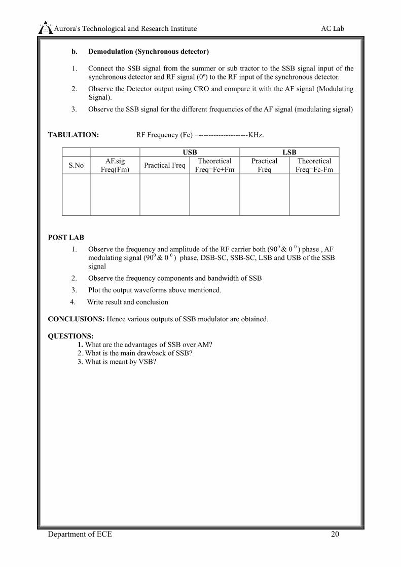
Auroras Technological and Research Institute AC Lab
Department of ECE 21
EXPERIMENT NO 4
FREQUENCY MODULATION AND DEMODULATION
OBJECTIVE To study
1 Frequency modulation process
2 Measurement of Modulation Index
3 Measurement of Frequency deviation
4 Demodulation Process
PRE-LAB 1 Study the data sheet of IC LM 2206 LM 565
2 Study the theory of FM modulation and demodulation
3 Draw the circuit diagram for modulation and demodulation
4 Draw the expected wave forms
EQUIPMENT 1 Frequency modulation and demodulation trainer kit 1 No 2 Dual trace CRO 1 No 3 Connecting probe and cords
THEORY
In telecommunications frequency modulation (FM) conveys information over a carrier
wave by varying its frequency (contrast this with amplitude modulation in which the amplitude
of the carrier is varied while its frequency remains constant) In analog applications the
instantaneous frequency of the carrier is directly proportional to the instantaneous value of the
input signal Digital data can be sent by shifting the carriers frequency among a set of discrete
values a technique known as keying The instantaneous frequency of the oscillator and is the
frequency deviation which represents the maximum shift away from fc in one direction
assuming xm(t) is limited to the range plusmn1Although it may seem that this limits the frequencies in
use to fc plusmn fΔ this neglects the distinction between instantaneous frequency and spectral
frequency The frequency spectrum of an actual FM signal has components extending out to
infinite frequency although they become negligibly small beyond a point Carsons rule of
thumb Carsons rule states that nearly all (~98) of the power of a frequency-modulated signal
lies within a bandwidth
Auroras Technological and Research Institute AC Lab
Department of ECE 22
CIRCUIT DIAGRAM
MODULATION
DEMODULATION
Auroras Technological and Research Institute AC Lab
Department of ECE 23
OUT PUT WAVEFORMS
Auroras Technological and Research Institute AC Lab
Department of ECE 24
PROCEDURE a Modulation
i Switch ON the trainer kit ii Generate the carrier and modulating signal iii apply the modulating signal to the frequency modulator iv Trace the FM output
b Demodulation i apply the modulated FM output into Demodulation input ii Trace the demodulated output waveform
TABULATION
SNo
Amplitude of Modulating
Signal(Am) Fmin
Frequency
Deviation
∆f=fc-fmin or fc-fmax
Modulation Index β=∆ffm
POST LAB
1 Observe the frequency and amplitude of the carrier and modulating signal 2 Calculate the frequency deviation by observing Fmax and Fmin
δ=Fc-Fmax or δ=Fc-Fmin
3 Calculate modulation index β= δFm
4 Change the amplitude of the modulating signal and repeat steps 1 to 3 for different values of Am and note down the readings in table-1
5 Plot the output waveforms Time T VS Voltage Vo
6 Write result and conclusion
CONCLUSIONS Hence the frequency modulated output is obtained
QUESTIONS 1 what is meant by angle modulation
2 How FM is different from AM
3 What is meant by Carson Rule
4 What is the maximum modulation index
Auroras Technological and Research Institute AC Lab
Department of ECE 25
EXPERIMENT NO 5
STUDY OF SPECTRUM ANALIZER AND ANALYSIS OF AM amp FM SIGNALS
Auroras Technological and Research Institute AC Lab
Department of ECE 26
Auroras Technological and Research Institute AC Lab
Department of ECE 27
Auroras Technological and Research Institute AC Lab
Department of ECE 28
EXPERIMENT NO 6
PRE EMPHASIS AND DE EMPHASIS
OBJECTIVE To study the operation of Pre-emphasis and De-emphasis circuits
PRE-LAB
1 Study the theory of Pre-emphasis and De-emphasis circuits
2 Draw the circuit diagram
3 Draw the expected waveforms
COMPONENTS
1 Resistors 100kΩ 100Ω
2 Capacitors 1μf 100μf EQUIPMENT 1 Function generator 1
2 Dual trace CRO 1
THEORY Pre-emphasis
Improving the signal to noise ratio by increasing the magnitude of higher frequency
signals with respect to lower frequency signals
De-emphasis
Improving the signal to noise ratio by decreasing the magnitude of higher
frequency signals with respect to lower frequency signals
Transmitters that employ a true FM modulator require a pre emphasis circuit before the
modulator fore the true FM modulator doesnt automatically pre emphasize the audio like
a transmitter that uses a phase modulator A separate circuit is not necessary for pre
emphasis in a transmitter that has a phase modulator because the phase modulator applies
pre emphasis to the transmitted audio as a function of the phase modulator The receivers
De emphasis circuitry takes the unnatural sounding pre emphasized audio and turns it
back into its original response Pre emphasized (discriminator) audio is however available
directly from the audio demodulation (discriminator) circuitry In linking systems many
choose to eliminate the emphasis circuitry to allow better representation of retransmitted
Auroras Technological and Research Institute AC Lab
Department of ECE 29
signals Since the signal has already been pre emphasized (by the user that is
transmitting) and since the receiver you are listening to takes care of the de emphasis
CIRCUIT DIAGRAMS
PRE-EMPHASIS
DE-EMPHASIS
EXPECTED WAVEFORMS
INPUT
TIME T
A
m
p
l i t u
d
e
Am
Auroras Technological and Research Institute AC Lab
Department of ECE 30
OUTPUT
PRE-EMPHASIS
Freq Vs Gain
DE-EMPHASIS
Freq Vs Gain
TIME T
Freq f (Hz)
A
m
p
l i t u
d
e
Am
Auroras Technological and Research Institute AC Lab
Department of ECE 31
TABLE
PRE EMPHASIS
SNo Input Freq
Input Voltage Vi (Volts)
Output Voltage Vo (Volts) Gain=VoVi
Gain in dB
20log(voVi)
DE-EMPHASIS
SNo Input Freq
Input Voltage Vi (Volts)
Output Voltage Vo (Volts)
Gain=VoVi Gain in dB
20log(VoVi)
PROCEDURE a Pre-emphasis
1 Connect the circuit as per the circuit diagram
2 Apply a constant sine wave input across the input terminal of fixed amplitude(Vi) 3 By varying the input frequency note down the output amplitude (Vo) with respect to
input frequency in Table 4 Calculate the gain using the formula
5 Gain =20log (Vo) (Vi) db
b De-Emphasis
1 Connect the circuit as per the circuit diagram
2 Repeat the steps 2 3 amp4
POST LAB
1 Observe the output amplitude for both the pre-emphasis and De-emphasis circuits
2 Calculate the gain in db
3 Plot the frequency versus gain curves on logarithmic graphs for both the circuits
4 Plot the input and output waveforms Time T VS Voltage Vo
5 Write the result and conclusion
CONCLUSIONS Obtained the pre emphasis and de-emphasis outputs
QUESTIONS 1 Observe the out put signal is disturbed by noise what action has to be taken and measure the
output voltage 2 Where we use the pre emphasis circuit 3 Where we use the de emphasis circuit 4 What are the advantages of pre emphasis and de emphasis circuits
Auroras Technological and Research Institute AC Lab
Department of ECE 32
EXPERIMENT NO 7
TIME DIVISION MULTIPLEXING AND DEMULTIPLEXING
AIM To study Time Division Multiplexing and its waveforms
PRE LAB WORK
Study the operation of Time division multiplexer and demultiplexer Draw the block diagram of TDM
Draw the expected graphs of all necessary waveforms ( CH1CH2TDM OP and Demultiplexed OP)
EQUIPMENT
1) Experimental board on TDM
2) Dual Trace CRO 3) Probes
THEORY
Time Division Multiplexing (TDM) is a technique for transmitting serial messages on a signal
transmission channel by dividing the time division into slots One slot for each message The concept
of TDM comes from sampling theorem which enables use to transmit the information contained in the
band limited Signal using sampling of the signal taken uniformly or a rate slightly higher then the
Nyquist rate TDM enables the joint utilization at a common transmission channel by a number of
independent message sources without mutual interference
The different Ip message signals all band limited in WHz by the IP low pass filters and sequentially
sampled at the transmitters by a rotary switch or a comparator The switch makes are complete
revolution in Ts frac12 W extracting are sample from each IP The commutator OP is a PAM waveform
containing individual message sample
It there are N number of IP the pulse to Pulse spacing will be Ts = 1 while the spacing
N Nfs
bw successive samples from each IP is called a frame
At the receiver a similar rotatory switch the decommutator separates the samples and distributes them
to a bank of low-pass filters which in turn is usually electronic and synchronization signals are
provided to keep the distribute in step with the commutant
Auroras Technological and Research Institute AC Lab
Department of ECE 33
EXPECTED GRAPHS
PROCUDURE
1 Connect the OP of the experimental board to one of the channels on CRO 2 Switch ON the experimental board 3 Observe the OP waveforms 4 Vary the values of the resistors R1 R2 and R3 alternative and observe the OP on CRO
RESULT
The process of the Time Division Multiplexing and the waveforms has been studied
CONCLUSION
Auroras Technological and Research Institute AC Lab
Department of ECE 34
Figure 1 Time Division Multiplexing amp De multiplexing
Auroras Technological and Research Institute AC Lab
Department of ECE 35
EXPERIMENT NO 9
VERIFICATION OF SAMPLING THEOREM
AIM To study the effect of sampling on the transmission of information through PWM
PRE LAB WORK
Study the sampling theorem
Draw the expected graphs of all necessary waveforms ( message signal carrier wave PWM op demodulated op etc
EQUIPMENT
1) Experimental Board on study of sampling theorem 2) Dual trace CRO (0 ndash 20 MHz) 3) Function Generator 4) Connecting wires
THEORY
The principle of sampling can be explained using the switching sampler The switch periodically shifts below bw two constants at the rate of fs = 1 Ts Hz staying on the IP constant for each sampling period The op Xs(t) of the samples consists of segments of x(t) and Xc(t) can be represented as
Xs(t) = X(t) S(t)
Where S(t) is sampling or switching function There are a number of differences bw the ideal sampling and reconstruction techniques described in the proceeding sections of the actual signal
PROCEDURE
1) Observe the internal clock and measure its frequency and amplitude 2) Give the clock to the clock IP terminal 3) Connect the modulating signal to the IP 4) Check the condition fs gt 2fm and observe the de-modulated wave 5) Check the condition fs lt 2fm and fs = 2fm and draw the OP waveforms
RESULT
CONCLUSION
Aurorarsquos Technological and Research Institute DC Lab
36
Figure 2 Sampling Theorem
Aurorarsquos Technological and Research Institute DC Lab
37
EXPERIMENT NO 10
PULSE AMPLITUDE MODULATION AND DEMODULATION
AIM 1) To study the PAM modulation and its waveforms
2) To study the de-modular of PAM
3) To study the effect of sampling frequency on de-modulation OP
PRE LAB WORK
Study the operation Pulse Amplitude Modulator and Demodulator Draw the block diagram of PAM modulator and demodulator Draw the expected graphs of all necessary waveforms ( message signal carrier wave PAM op
demodulated op etc)
EQUIPMENT
1) Exp Board on study of PAM 2) CRO 3) Functional Generator 4) Connecting wires and chords
THEORY
In PAM the amplitude of the carrier wave of higher frequency follow the amp of the message signal
Within this (Modulation Sampling) we have two more types of sampling those are
(1) Natural Sampling
(2) Flat Top Sampling
Basically in Natural Sampling the carrier waves are train of pulses of a certain frequency After
sampling the top of the Pulse follow the message signal Due to this following of top of Pulses with the
message signals cause a distortion in De-modulation
In Flat top sampling also we use train of pulses for sampling but only the starting point of each pulse
follow the message signal remaining width of the pulse will (follow) be flat But here we go for Natural
sampling
EXPECTED WAVEFORMS
Aurorarsquos Technological and Research Institute DC Lab
38
PROCEDURE (MODULATION)
1 Observe the clock on CRO and measure its frequency and amp (freq 5KHz) 2 Connect the clock to clock IP terminals in modulation 3 Put control switch in ac position and set amplitude = OV This provides DC at Modulating
signal terminal 4 Connect the modulating signal or IP to the modulator 5 Connect one channel of CRO at lsquoTirsquo and Gnd Observe that the pulses are of same height
Height is adjustable by varying offset This is PAM signal with DC IP Measure amplitude and frequency of Pulses
6 Increase the amplitude of modulation signal Observe the amplitude and frequency of this sinusoidal modulating signal
7 Observe PAM signal
a) How many Pulses are there in one modulating cycle
b) It is natural or Flat Top PAM c) It is Single or dual polarity PAM
8 Observe the effect of DC offset on PAM waveform
DE-MODULATION
1) Generate undistorted PAM waveform 2) Connect the modulating signal to de-modulation IP 3) Observe the detected OP and measure its frequency which must be same as
modulating signal
EFFECT OF SAMPLING FREQUENCY
1) Connect internal sinusoidal signal to modulating signal IP of the modulator 2) Connect an external functional Generator at the circuit terminals of the modulator 3) Get the PAM waveform using the above circuit 4) Adjust the modulating amplitude offset and frequency to get an undistorted frequency 5) Connect the PAM to de-modulator IP 6) Observe the demodulated signal for various frequencies of clock (fs gt 2fm lt 2fm = 2 fm)
RESULT
CONCLUSION
Aurorarsquos Technological and Research Institute DC Lab
39
Figure 3 Pulse Amplitude Modulation
Auroras Technological and Research Institute AC Lab
Department of ECE 5
EXPERIMENT NO 11
PULSE WIDTH MODULATION AND DEMODULATION
AIM
1) To study the PWM process and the corresponding waveforms 2) To study the effect of sampling frequency on the transmission of information through PWM
PRE LAB WORK
Study the operation Pulse Width Modulator and Demodulator Draw the block diagram of PWM modulator and demodulator Draw the expected graphs of all necessary waveforms ( message signal carrier wave PWM op
demodulated op etc
EQUIPMENT
1) Experimental Board
2) Dual trace CRO 3) AF generator 4) Multimeter
THEORY
In PWM the samples of the message signal are used to vary the duration of the individual pulses The
pulse width may be varied by varying the time of occurrence of the leading edge trailing edge of both
edges of the pulse in accordance with the sampled value of the modulating wave PWM can also be
generated by using emitter follower monostable multivibrator is an excellent voltage to time converter
since its gate width is dependent on the voltage to which the capacitor is changed If this voltage can be
varied in accordance with a signal voltage a series of rectangular pulses can be obtained with width
varying as required
The demodulated of PWM is quite simple PWM is passed through a low pass filter The reconstruction is
associated with a certain amount of Distortion caused by the cross modulator products that fall in the
signal band
EXPECTED WAVEFORM
Aurorarsquos Technological and Research Institute DC Lab
41
PROCEDURE
STUDY OF MODULATION
1) Observe the clock on CRO and measure its frequency (fs) 2) Observe the sine wave modulating signal on CRO and observe the dc shift produced in this
by varying the offset nob Measure the frequency Variation limits of this signal 3) Apply clock at the circuit input terminal 4) Apply modulating signal by keeping the control switch in dc position 5) Observe the modulated wave 6) Plot the graph bw pulse width and the applied dc voltage 7) Put the control switch in sine wave position and adjust the modulating signal amplitude
frequency and dc offset to get the stationary waveform of PWM 8) Note the number of pulses in one circuit of modulating signal
STUDY OF DEMODULATION
1) Generate the stationary PWM waveform using sin wave modulating signal 2) Connect the modulator OP to PWM demodulator 3) Connect Channel (1) to Modulating Signal and channel (2) to demodulated wave
EFFECT OF SAMPLING FREQUENCY
1) Use an external square wave and connect it to the clock input 2) Set the frequency of square wave at frequency 2fm 3) Observe the demodulated wave
4) Change the frequency of square wave to fs lt 2fm fs gt 2fm and observe the demodulated wave
RESULT
CONCLUSION
Aurorarsquos Technological and Research Institute DC Lab
42
Figure 4 Pulse Width Modulation
Aurorarsquos Technological and Research Institute DC Lab
43
EXPERIMENT NO 12
PULSE POSITION MODULATION AND DEMODULATION
AIM
1) To study the PPM Modulation and the corresponding waveforms 2) To study the de-modulation of PPM 3) To see the effect of sampling frequency on the transmission of information through PPM
PRE LAB WORK
Study the operation Pulse Position Modulator and Demodulator Draw the block diagram of PPM modulator and demodulator Draw the expected graphs of all necessary waveforms ( message signal carrier wave PPM op
demodulated op etc
EQUIPMENT
1) Experimental Board for PPM
2) Dual Phase Oscilloscope
3) AF Generator
THEORY
In PDM long pulses expand considerable power duration If the pulse which bearing no additional
information If this un used power is subtracted from PDM so that only time transitions are preserved
We observe a more efficient type of pulse modulation known as pulse position modulation Here in the
Pulse Position Modulated wave the position of the Pulse relative to its unmodulated time of occurrence is
varied in accordance with the message signal
We generate a PPM wave from PWM wave by using a Monostable Multivibrator The device has one
absolutely stable state and one quest ndash stable state into which it is triggered by an externally applied Pulse
The monostable multivibrator is designed to trigger on the trailing edges of the duration ndash modulated pulse
is varied in accordance with the message signal
The fixed pulse duration of the PPM wave at the monostable multivibrator OP can be set by appropriately
choosing the resistance ndash capacitance combination in the timing circuit of the device
Aurorarsquos Technological and Research Institute DC Lab
44
EXPECTED WAVEFORM
PROCEDURE
STUDY OF MODULATION
Observe the clock and measure its frequency (fs) Apply the clock at the clock IP terminal in the modulator Apply the modulating signal keeping control switch in DC position Observe the PPM OP Connect the channel ndash (1) on CRO to clock and channel (2) to PPM wave OP Compare the position of two waveforms Vary the DC offset and observe the relative shift between the clock and PPM OP Measure the time shift between clock and PPM wave for various settings of offset Draw the graph between time shift and DC voltage Put the control switch in AC position adjusts the amplitude and frequency and offset
of sinusoidal modulating signal to get the stationary PPM wave Note the number of pulses in one cycle of the modulated wave
STUDY OF DEMODULATION
Generate a stationery PPM wave for a sinusoidal modulating signal Apply the PPM wave to the input of de-modulator Connect the Channel ndash (1) of CRO to the modulating signal and channel ndash 2 to the
de-modulator output Compare the two waveforms
Note the frequency of demodulated wave It should be same as the modulating signal Note down the waveform
RESULT
CONCLUSION
Aurorarsquos Technological and Research Institute DC Lab
45
Aurorarsquos Technological and Research Institute DC Lab
46
Figure 5 Pulse Position Modulation
Aurorarsquos Technological and Research Institute AC Lab
47
EXPERIMENT NO 13
FREQUENCY SYNTHESIZER
AIM
To study the operation of frequency synthesizer using PLL
PRE-LAB 1 Study the data sheet of IC 7404IC 4017IC 565 and IC 4046
2 Study the theory of frequency synthesizer 3 Draw the circuit diagram and expected waveforms
EQUIPMENTS
1 Frequency synthesizer trainer AET -26A
2 Dual trace CRO (20Mhz) 3 Digital frequency counter or multimeter
4 Patch chords
THEORY
A frequency synthesizer is an electronic system for generating any of a range
of frequencies from a single fixed time base or oscillator They are found in many modern
devices including radio receivers mobile telephones radiotelephones walkie-talkies CB
radios satellite receivers GPS systems etc A frequency synthesizer can combine
frequency multiplication frequency division and frequency mixing (the frequency mixing
process generates sum and difference frequencies) operations to produce the desired output
signal
BLOCK DIAGRAM
Phase Comparator
Amplifier Low pass filter
V C O
Div N Network frequency divider
Fin= fout
N
fin
Fout =Nf in
Aurorarsquos Technological and Research Institute AC Lab
48
SIMPLE 1KHZ-9KHZ FREQUENCY SYNTHESIZER
CIRCUIT DAIGRAM
PROCEDURE 1 Switch on the trainer ad verify the output of the regulated power supply ie 5V These
supplied are internally connected to the circuit so no extra connections are required 2 Observe output of the square wave generator using oscilloscope and measure the range
with the help of frequency counter frequency range should be around 1KHz to 10KHz 3 Calculate the free running frequency range of the circuit (VCO output between 4th pin
and ground 1 For different values of timing resistor R1 ( to measure Rt value using digital multimeter between given test points 1 And record the frequency values in table 1
Fout = 03 (RtCt) where Rt is the timing resistor and Ct is the timing capacitor = 001 f
Aurorarsquos Technological and Research Institute AC Lab
49
4 Connect 4th pin of LM 565 (Fout) to the driver stage and 5th pin (Phase comparator) connected to 11th pin of 7404 Output can be taken at the 11th pin of the 7490 It should be divided by the 2 amp 3 times of the fout
TABULATION
Fin KHz Fout = N x fin KHz Divided by 3 2
EXPECTED WAVEFORMS
POST LAB
1 Observe the synthesized output in table 2 Calculate the output frequency
3 Plot the output waveforms
4 Write result and conclusions
CONCLUSIONS
The various outputs of frequency synthesizer are verified
QUESTIONS
1 What are the applications of frequency synthesizer
TIME T
A
m
p
l i T
u
d
e
Ac
Aurorarsquos Technological and Research Institute AC Lab
50
2 What is the difference between heterodyning and synthesizer
Aurorarsquos Technological and Research Institute AC Lab
51
EXPERIMENT NO 14
AGC CHARATERISTICS
AIM
To observe the effect of automatic gain control(AGC)
PRE LAB 1 To study the theory of AGC 2 Draw the Block Diagram circuits diagram and expected waveforms
EQUIPMENTS 1 AGC Trainer Kit 2 CRO
3 Patch Chords
4 Digital Multimeter
THEORY
Automatic gain control (AGC) is an adaptive system found in many electronic
devices The average output signal level is fed back to adjust the gain to an appropriate level
for a range of input signal levels For example without AGC the sound emitted from an AM
radio receiver would vary to an extreme extent from a weak to a strong signal the AGC
effectively reduces the volume if the signal is strong and raises it when it is weaker AGC
algorithms often use a PID controller where the P term is driven by the error between
expected and actual output amplitude
Block Diagram
Frequency Converter
1st IF Amplifier
2nd IF Amplifier
Detector
Audio Preamplifier
Driver Output
Aurorarsquos Technological and Research Institute AC Lab
52
CIRCUIT DIAGRAM
PROCEDURE
1 Connect 455 KHz IF Signal Function Generator connect AGC link Connect CRO channel-1 at input terminals
2 Connect CRO channel 2 at collector of Q3 The amplified signal will be observed 3 Calculate the voltage gain by measuring the amplitude of output signal (Vo) waveform
using formula A=VoVi 4 Now connect CRO-2 channel at output The detected audio signal of 455 Khz will be
observed 5 Now vary input level of 455 KHz IF signal and observe detected 455 KHz audio signal
with and without AGC link The output will be distorted when AGC link is removed ie there is no AGC action
6 This explains AGC effect in Radio circuit
TABULATION
SNo Input Voltage Vi (P-P) With out AGC With AGC
Output Voltage Vo (P-P)
Gain A= Vo Vi
Output Voltage Vrsquoo (P-P)
Gain Arsquo= Vrsquoo Vi
Aurorarsquos Technological and Research Institute AC Lab
53
EXPECTED WAVEFORMS
AM Modulated RF Input
Detected Output with AGC
Detected Output without AGC
POST-LAB
1 Observe the input voltage and output voltage for with AGC and Without AGC in Table 1
2 Calculate Gain a=vovi for both cases 3 Plot the output waveforms Time T Vs Voltage Vo and input voltage Vi Vs Gain A 4 Write Result and Conclusions
CONCLUSIONS The AGC characteristics are verified
QUESTIONS 1 what is meant by AGC
2 What is the difference between simple AGC and delayed AGC
3 From which part of receiver AGC is obtained
TIME T
A
m
p
l i T
u
d
e
Ac
TIME T
A
m
p
l i T
u
d
e
Ac
TIME T
A
m
p
l i T
u
d
e
Ac
Aurorarsquos Technological and Research Institute AC Lab
54
EXPERIMENT NO 15
PHASE LOCKED LOOP
OBJECTIVE To study the Phase locked loop using 565 IC and to take input frequency given by an external signal source
PRE-LAB To Study
1 The data sheet of IC 565
2 The theory of Phase locked loop
3 About free running frequency locking range and capture range
4 Draw the circuit diagram and expected waveforms
EQUIPMENT 1 Function generator 2
2 Dual trace CRO 1
3 Phase locked loop trainer kit
THEORY
A phase-locked loop or phase lock loop (PLL) is a control system that generates a signal
that has a fixed relation to the phase of a reference signal A phase-locked loop circuit
responds to both the frequency and the phase of the input signals automatically raising or
lowering the frequency of a controlled oscillator until it is matched to the reference in both
frequency and phase A phase-locked loop is an example of a control system using negative
feedback Phase-locked loops are widely used in radio telecommunications computers and
other electronic applications They may generate stable frequencies recover a signal from a
noisy communication channel or distribute clock timing pulses in digital logic designs
such as microprocessors Since a single integrated circuit can provide a complete phase-
locked-loop building block the technique is widely used in modern electronic devices
with output frequencies from a fraction of a cycle per second up to many gigahertz
BLOCK DIAGRAM
Aurorarsquos Technological and Research Institute AC Lab
55
CIRCUIT DIAGRAM
PROCEDURE 1 Switch ON the trainer kit 2 Check the VCO output at pin 4 of IC 565 that is a square wave form The frequency of the
VCO Output depends on CT (001f) and RT (47kΩ) 3 Next short the pins 4amp5 and give signal of variable frequency and observe VCO output 4 Change the input frequency and observe the VCO output on the CRO 5 Between some frequencies the VCO output is locked to the input signal frequency This can
be observed by increasing or decreasing the frequency of the VCO output by changing input frequency
6 Before or after that frequency range the VCO output is not locked
7 Calculate Lock range (FL) and capture range (FC) by using the following formulas
FL = 8foVCO fo=03RtCT
FC=12π radic2πf236103 C2
Table1
SNo Locking Frequency Frequency Range From To
CHARTERISTICES
Aurorarsquos Technological and Research Institute AC Lab
56
CONCLUSIONS Obtained the lock range of PLL
QUESTIONS
1 Observe the VCO output when pins 4amp5 short and give square wave as signal 2 Define lock range and capture range
3 What are the basic applications of PLL
Aurorarsquos Technological and Research Institute AC Lab
57
ANNEXURE-I
EXPERIMENT NO 1
Aurorarsquos Technological and Research Institute AC Lab
58
CHARACTERISTICS OF MIXER
AIM
To study the functioning of a frequency mixer
PRE LAB 1 To study the theory of Mixer 2 Draw the circuit diagram and expected waveforms
EQUIPMENTS 1 Frequency mixer trainer kit 2 CRO (20MHz) 3 Connecting cords and probes 4 Function generator (1MHz)
THEORY
In receivers using the super heterodyne principle a signal at variable frequency is
converted to a fixed lower frequency IF before detection IF is called the intermediate frequency
In typical AM (Amplitude Modulation eg as used on medium wave) home receivers that
frequency is usually 455 kHz for FM VHF receivers it is usually 107 MHz An intermediate
frequency (IF) is a frequency to which a carrier frequency is shifted as an intermediate step in
transmission or reception Frequency modulation (FM) is a form of modulation that represents
information as variations in the instantaneous frequency of a carrier wave Very high frequency
(VHF) is the radio frequency range from 30 MHz (wavelength 10 m) to 300 MHz (wavelength 1
heterodyne receivers mix all of the incoming signals with an internally generated waveform
called the local oscillator The user tunes the radio by adjusting the sets oscillator frequency in
the mixer stage of a receiver the local oscillator signal multiplies with the incoming signals
which shifts them all down in frequency The one that shifts is passed on by tuned circuits
amplified and then demodulated to recover the original audio signal The oscillator also shifts a
copy of each incoming signal up in frequency by amount Those very high frequency images
are all rejected by the tuned circuits in the IF stage The Super heterodyne receiver (or to give it its
full name The Supersonic Heterodyne Receiver usually these days shortened to superhet) was
invented by Edwin Armstrong in 1918
Aurorarsquos Technological and Research Institute AC Lab
59
BLOCK DIAGRAM
CIRCUIT DIAGRAM
EXPECTED WAVEFORMS
INPUT SIGNAL Fx
INPUT SIGNAL Fy
TIME T
A
m
p
l i T
u
d
e
Ac
Aurorarsquos Technological and Research Institute AC Lab
60
MIXER OUTPUT(Fy-Fx)
PROCEDURE 1 Connect the circuit as per the given circuit diagram 2 Switch on the power supply of trainer kit 3 Apply a sine wave at input Fx of 2 VP-P amplitude and 100 KHz frequency 4 Apply a sine wave at input FY of 2 VP-P amplitude and 100 KHz frequency 5 Observe the output waveform on the CRO 6 Repeat the steps 34 and 5 by changing the values of Fx once greater than and less than
FY in a steps of 5Khz (in the range 80KHz to 120KHz)
TABULATION
TIME T
A
M
P
L
I T
U
D
E
TIME T
A
m
p
l i T
u
d
e
Ac
Aurorarsquos Technological and Research Institute AC Lab
61
SNo Freq (Fy)
(kHz) Amp(V) Freq(Fx) (kHz) Amp(V) Freq(Fy-Fx)
(kHz) Amp(V)
POST LAB 1 Observe the amplitude and time Of inputs and output in table
2 Draw the expected waveforms
3 Verify the output signal obtained with the theoretical value 4 Plot the graphs for Time T VS input signal (FX) Voltage V input signal (FY) Voltage V
and output Signal F(x-y) voltage V 5 Write result and conclusions
CONCLUSIONS
Obtained the output of the mixer for various inputs
QUESTIONS
1 what are the different types of mixtures available
2 What is meant by heterodyning
3 What is meant by IF
Aurorarsquos Technological and Research Institute AC Lab
62
EXPERIMENT NO 2
DIGITAL PHASE DETECTOR
OBJECTIVE To detect the phase difference between two square wave signals using digital phase detector
PRE LAB
1 To study the theory of digital phase detector and EX-OR gate operation and truth table 2 Draw the circuit diagram and expected output and input waveforms
EQUIPMENT 1 Digital phase detector trainer kit 2 Regulated power supplies
3 CRO (20MHz) 4 Connecting cords amp probes
5 Digital frequency counter or multimeter
THEORY
Phase detector is a frequency mixer or analog multiplier circuit that generates a voltage
signal which represents the difference in phase between two signal inputs It is an essential
element of the phase-locked loop (PLL)Detecting phase differences is very important in many
applications such as motor control radar and telecommunication systems servo mechanisms and
demodulators
Electronic phase detector
Some signal processing techniques such as those used in radar may require both the amplitude
and the phase of a signal to recover all the information encoded in that signal One technique is to
feed an amplitude-limited signal into one port of a product detector and a reference signal into the
other port the output of the detector will represent the phase difference between the signals If the
signal is different in frequency from the reference the detector output will be periodic at the
difference frequency Phase detectors for phase-locked loop circuits may be classified in two
types A Type I detector is designed to be driven by analog signals or square-wave digital signals
and produces an output pulse at the difference frequency The Type I detector always produces an
output waveform which must be filtered to control the phase-locked loop variable frequency
oscillator (VCO) A type II detector is sensitive only to the relative timing of the edges of the input
and reference pulses and produces a constant output proportional to phase difference when both
signals are at the same frequency This output will tend not to produce ripple in the control voltage
of the VCO
Aurorarsquos Technological and Research Institute AC Lab
63
BLOCK DIAGRAM OF PLL
CIRCUIT DIAGRAM
Aurorarsquos Technological and Research Institute AC Lab
64
EXPECTED WAVEFORMS
EX-OR PHASE DETECTOR
EDGE TRIGGERED OUTPUT
PROCEDURE
1 Switch on the trainer kit
2 Observe the output of the square wave generator available on the trainer kit using CRO
and measure the range with the help of frequency counter the frequency range should be
around 2 KHz to 13 KHz
3 Calculate the free running range of the VCO output ie between 4th pin of IC PLL 565
and ground For different values of timing resistor Rt fout is given by Fout =03 Rt Ct
where Ct timing capacitor = 001 μF Rt timing resistor
4 Connect the square wave to the input of IC PLL 565 and short 4th and 5th pin of PLL
Vary the input frequency of the square wave when the PLL is locked that is connected to
Aurorarsquos Technological and Research Institute AC Lab
65
one input fout EX-OR phase detector The other input fin of EX-OR phase detector is the
coming from inbuilt of square wave generator
5 Connect the pulse generator output to the input of IC 565 PLL and short 4th amp 5th pin of
PLL Vary the input frequency of the square wave when the PLL is locked that is
connected to one input of Edge triggered phase detector input ie fout The other input fin
of edge triggered phase detector is the pulse input coming from the inbuilt pulse generator
6 The dc output voltage of the exclusive-OR phase detector is a function of the phase
difference between its two inputs fin and fout
POST LAB
1 Observe the Voltage and Time of the two input square waves
2 Observe difference of two inputs as square wave output
3 Plot the inputs and output waveforms Time T VS Voltage V
CONCLUSIONS
The phase detector outputs are verified
QUESTIONS
1 What is the function of phase detector
2 What is the condition for getting maximum output
3 Advantages of digital phase detector over analog phase detector
Aurorarsquos Technological and Research Institute AC Lab
66
EXPERIMENT NO 3
COASTAS RECEIVER
AIM
To demodulate a DSB-SC signal using coastas receiver
PRE LAB 1 To study the operation of coastas receiver 2 Draw the circuit diagram and expected waveforms
EQUIPMENTS 1 Communications trainer kit 2 DSB-SC modulator trainer kit 3 CRO (20MHz) 4 Connecting cords and probes 5 Function generator (1MHz)
THEORY
This loop and its variations is much-used as a method of carrier acquisition (and
simultaneous message demodulation) in communication systems both analog and digital
It has the property of being able to derive a carrier from the received signal even when there is
no component at carrier frequency present in that signal (eg DSBSC) The requirement is that
the amplitude spectrum of the received signal be symmetrical about this frequency
The Costas loop is based on a pair of quadrature modulators - two multipliers
fed with carriers in phase-quadrature These multipliers are in the in-phase (I) and quadrature
phase (Q) arms of the arrangement Each of these multipliers is part of separate synchronous
demodulators The outputs of the modulators after filtering are multiplied together in a third
multiplier and the lowpass components in this product are used to adjust the phase of the local
carrier source - a VCO - with respect to the received signal The operation is such as to
maximise the output of the I arm and minimize that from the Q arm The output of the I arm
happens to be the message and so the Costas loop not only acquires the carrier but is a
(synchronous) demodulator as well A complete analysis of this loop is non-trivial It would
include the determination of conditions for stability and parameters such as lock range capture
range and so on
Aurorarsquos Technological and Research Institute AC Lab
67
BLOCK DIAGRAM
EXPECTED WAVEFORMS
DSB-SC modulated output
Aurorarsquos Technological and Research Institute AC Lab
68
Demodulated output of the coastas loop
PROCEDURE
1 Switch ON the DSB-SC trainer kit
2 Generate the carrier and modulating signal
3 Generate the DSB-SC modulated signal
4 Connect the required blocks of the coastas receiver in the communications kit
5 Apply the generated DSB-SC signal to the above connected coastas receiver
6 Observe that the output of the coastas receiver is the demodulated wave of DSB-SC signal
POST LAB
1 Observe the frequency and amplitude of the carrier and modulating signal
2 Observe the frequency and amplitude of the balanced modulator output
3 Observe the lock condition of the coastas loop
4 observe the output of the coastas demodulator
5 Write result and conclusions
CONCLUSIONS The balanced modulator output and the operation of coastas receiver is verified
QUESTIONS 1 what is the operation of coastas loop
2 What happens when the locking condition of the coastas loop occurs
3 Coastas loop can be used for demodulation of other modulation techniques also What are they
Aurorarsquos Technological and Research Institute AC Lab
69
MATLAB PROGRAMMES
Aurorarsquos Technological and Research Institute AC Lab
70
INDEX
1 Introduction - 70
2 Amplitude Modulation and Demodulation - 74
3 DSB-SC Modulation and Demodulation - 84
4 SSB-SC Modulation and Demodulation - 89
5 Frequency Modulation and Demodulation - 95
6 Phase Modulation and Demodulation - 99
7 Time Division Multiplexing and Demultiplexing - 100
8 Frequency Division Multiplexing and Demultiplexing- 103
9 Verification of Sampling Theorem - 104
10 Pulse Amplitude Modulation and Demodulation - 106
11 Pulse width Modulation and Demodulation - 108
12 Pulse Position Modulation and Demodulation - 110
13 PLL as FM Demodulator - 112
Aurorarsquos Technological and Research Institute AC Lab
71
1 INTRODUCTION
What Is Simulink
Simulink is a software package for modeling simulating and analyzing dynamic
systems It supports linear and nonlinear systems modeled in continuous time sampled time
or a hybrid of the two Systems can also be multirate ie have different parts that are
sampled or updated at different rates
Tool for Simulation
Simulink encourages you to try things out You can easily build models from scratch
or take an existing model and add to it You have instant access to all the analysis tools in
MATLABreg so you can take the results and analyze and visualize them A goal of Simulink
is to give you a sense of the fun of modeling and simulation through an environment that
encourages you to pose a question model it and see what happens
Simulink is also practical With thousands of engineers around the world using it to
model and solve real problems knowledge of this tool will serve you well throughout your
professional career
Tool for Model-Based Design
With Simulink you can move beyond idealized linear models to explore more realistic
nonlinear models factoring in friction air resistance gear slippage hard stops and the other
things that describe real-world phenomena Simulink turns your computer into a lab for
modeling and analyzing systems that simply wouldnt be possible or practical otherwise
whether the behavior of an automotive clutch system the flutter of an airplane wing the
dynamics of a predator-prey model or the effect of the monetary supply on the economy
For modeling Simulink provides a graphical user interface (GUI) for building models
as block diagrams using click-and-drag mouse operations With this interface you can draw
the models just as you would with pencil and paper (or as most textbooks depict them) This
is a far cry from previous simulation packages that require you to formulate differential
equations and difference equations in a language or program Simulink includes a
comprehensive block library of sinks sources linear and nonlinear components and
connectors You can also customize and create your own blocks For information on creating
your own blocks see the separate Writing S-Functions guide
Models are hierarchical so you can build models using both top-down and bottom-up
approaches You can view the system at a high level then double-click blocks to go down
through the levels to see increasing levels of model detail This approach provides insight into
how a model is organized and how its parts interact
After you define a model you can simulate it using a choice of integration methods either
from the Simulink menus or by entering commands in the MATLAB Command Window The
menus are particularly convenient for interactive work while the command-line approach is
very useful for running a batch of simulations (for example if you are doing Monte Carlo
simulations or want to sweep a parameter across a range of values) Using scopes and other
display blocks you can see the simulation results while the simulation is running In addition
Aurorarsquos Technological and Research Institute AC Lab
72
you can change many parameters and see what happens for what if exploration The
simulation results can be put in the MATLAB workspace for post processing and
visualization
Model analysis tools include linearization and trimming tools which can be accessed
from the MATLAB command line plus the many tools in MATLAB and its application
toolboxes And because MATLAB and Simulink are integrated you can simulate analyze
and revise your models in either environment at any point
1 Generation of cosine wave in time domain and frequency
domain Clc clear all close all x = -500015 t = 0140001 time = cos(23141000t) y1 = cos(23141000x) subplot(211) plot(xy1) axis([-5 5 -3 3]) grid on title(Time domain) xlabel(Time ) ylabel(Amplitude) now create a frequency vector for the x-axis and plot the magnitude and phase subplot(212) fre = abs(fft(time)) f = (0length(fre) - 1)4000length(fre) plot(ffre) grid on title(Frequency domain (Spectrum)) xlabel(Freq ) ylabel(Amplitude)
WAVEFORMS
Aurorarsquos Technological and Research Institute AC Lab
73
2 Generation of square wave in time domain and frequency
domain
clc clear all close all x = -500015 Fs = 399 t = 01Fs1 time = SQUARE(2pi1000t) y1 = SQUARE(23141000x) subplot(211) plot(xy1) axis([-5 5 -3 3]) grid on xlabel(Time domain) ylabel(Amplitude) now create a frequency vector for the x-axis and plot the magnitude and phase subplot(212) fre = abs(fft(time)) f = (0length(fre) - 1)Fslength(fre) plot(ffre) grid on xlabel(Freq domain) ylabel(Amplitude)
WAVEFORMS
Aurorarsquos Technological and Research Institute AC Lab
74
Aurorarsquos Technological and Research Institute AC Lab
75
2 AMPLITUDE MODULATION AND DEMODULATION PROGRAM 1
clc clear all close all Ac=1 Carrier Amplitude Fc=04 Carrier frequency Fm=005 baseband frequency Fs=10 sampling t=001200 mt=cos(2piFmt) under modulation mu=05 st=Ac(1+mumt)cos(2piFct) subplot(211) plot(tst) hold on plot(tAc(mumt+ones(1length(mt)))r) plot(t-Ac(mumt+ones(1length(mt)))r) hold off title(Modulation Index = 05 under modulation Ac(1+05cos(2pi005t))cos(2pi04t)) xlabel(time (s))ylabel(amplitude) st_fft=fft(st) st_fft=fftshift(st_fft) st_fft_fre=5linspace(-11length(st_fft)) subplot(212) plot(st_fft_freabs(st_fft)) title(spectrum with Modulation Index = 05) xlabel(Frequency (Hz))axis([-1 1 0 1000Ac+100])
total modulation figure mu=1 st=Ac(1+mumt)cos(2piFct) subplot(211) plot(tst) hold on plot(tAc(mumt+ones(1length(mt)))r) plot(t-Ac(mumt+ones(1length(mt)))r) hold off title(Modulation Index = 1 modulation Ac(1+1cos(2pi005t))cos(2pi04t)) xlabel(time (s))ylabel(amplitude) st_fft=fft(st) st_fft=fftshift(st_fft) st_fft_fre=Fs2linspace(-11length(st_fft)) subplot(212) plot(st_fft_freabs(st_fft)) title(spectrum with Modulation Index = 1) xlabel(Frequency (Hz))axis([-1 1 0 1000Ac+100])
Aurorarsquos Technological and Research Institute AC Lab
76
over Modulation figure mu=2 st=Ac(1+mumt)cos(2piFct) subplot(211) plot(tst) hold on plot(tAc(mumt+ones(1length(mt)))r) plot(t-Ac(mumt+ones(1length(mt)))r) hold offtitle(Modulation Index = 2 over modulation Ac(1+2cos(2pi005t))cos(2pi04t)) xlabel(time (s))ylabel(amplitude) st_fft=fft(st) st_fft=fftshift(st_fft) st_fft_fre=Fs2linspace(-11length(st_fft)) subplot(212) plot(st_fft_freabs(st_fft)) title(spectrum with Modulation Index = 2) xlabel(Frequency (Hz))axis([-1 1 0 1000Ac+100])
WAVEFORMS
Aurorarsquos Technological and Research Institute AC Lab
77
PROGRAM 2
Aurorarsquos Technological and Research Institute AC Lab
78
task 1 fc=154000
task 2 fm=fc10 fs=100fc t=01fs4fm xc=cos(2pifct) xm=cos(2pifmt) figure(1) subplot(211)plot(txc) title(carrier signal of 154 khz) xlabel(time (sec)) ylabel(amplitude) subplot(212)plot(txm) title(message signal of 154 khz) xlabel(time (sec)) ylabel(amplitude) DSB-SC MODULATION mu = input( enter the Modulation Index value ) z1=(1+muxm)xc figure(2)
task 31 subplot(211)plot(tz1) title(AMPLITUDE MODULATION IN TIME DAOMAIN) xlabel(time (sec)) ylabel(amplitude)
task 32 l1=length(z1) f=linspace(-fs2fs2l1) Z1=fftshift(fft(z1l1)l1) subplot(212)plot(fabs(Z1)) title(AMPLITUDE MODULATION IN FREQUENCY DOMAIN) xlabel(frequency(hz)) ylabel(amplitude) axis([-200000 200000 0 03])
task 33 demodulation s1=z1xc S1=fftshift(fft(s1length(s1))length(s1)) figure(3) plot(fabs(S1)) title( demodulated signal IN FREQUENCY DOMAIN before filtring) xlabel(frequency(hz)) ylabel(amplitude) axis([-200000 200000 0 03]) hold on Hlp=1sqrt(1+(ffc)^(2100)) plot(fHlpr) title( frequency response of low pass filter) xlabel(frequency(hz)) ylabel(amplitude) axis([-200000 200000 0 2])
task 34 E1=HlpS1 figure(4) subplot(211)plot(fE1)
Aurorarsquos Technological and Research Institute AC Lab
79
title( Recover signal IN FREQUENCY DOMAIN after filtring) xlabel(frequency(hz)) ylabel(amplitude) axis([-200000 200000 0 03]) e1=ifft(ifftshift(E1))length(E1) subplot(212)plot(t(105)e1) title( Recover signal IN Time DOMAIN after filtring) xlabel(time(sec)) ylabel(amplitude)
WAVEFORMS
enter the Modulation Index value 05
0 1 2 3
x 10-4
-1
-05
0
05
1carrier signal of 154 khz
time (sec)
am
plit
ude
0 1 2 3
x 10-4
-1
-05
0
05
1message signal of 154 khz
time (sec)
am
plit
ude
Aurorarsquos Technological and Research Institute AC Lab
80
0 1 2 3
x 10-4
-2
-1
0
1
2AMPLITUDE MODULATION IN TIME DAOMAIN
time (sec)
am
plit
ude
-2 -15 -1 -05 0 05 1 15 2
x 105
0
01
02
AMPLITUDE MODULATION IN FREQUENCY DOMAIN
frequency(hz)
am
plit
ude
-2 -15 -1 -05 0 05 1 15 2
x 105
0
02
04
06
08
1
12
14
16
18
2 frequency response of low pass filter
frequency(hz)
am
plit
ude
Aurorarsquos Technological and Research Institute AC Lab
81
enter the Modulation Index value 1
-2 -15 -1 -05 0 05 1 15 2
x 105
0
01
02
Recover signal IN FREQUENCY DOMAIN after filtring
frequency(hz)
am
plit
ude
0 1 2 3
x 10-4
05
1
15
2 Recover signal IN Time DOMAIN after filtring
time(sec)
am
plit
ude
0 1 2 3
x 10-4
-2
-1
0
1
2AMPLITUDE MODULATION IN TIME DAOMAIN
time (sec)
am
plit
ude
-2 -15 -1 -05 0 05 1 15 2
x 105
0
01
02
AMPLITUDE MODULATION IN FREQUENCY DOMAIN
frequency(hz)
am
plit
ude
Aurorarsquos Technological and Research Institute AC Lab
82
enter the Modulation Index value 2
-2 -15 -1 -05 0 05 1 15 2
x 105
0
02
04
06
08
1
12
14
16
18
2 frequency response of low pass filter
frequency(hz)
am
plit
ude
-2 -15 -1 -05 0 05 1 15 2
x 105
0
01
02
Recover signal IN FREQUENCY DOMAIN after filtring
frequency(hz)
am
plit
ude
0 1 2 3
x 10-4
0
1
2
3 Recover signal IN Time DOMAIN after filtring
time(sec)
am
plit
ude
Aurorarsquos Technological and Research Institute AC Lab
83
0 1 2 3
x 10-4
-4
-2
0
2
4AMPLITUDE MODULATION IN TIME DAOMAIN
time (sec)
am
plit
ude
-2 -15 -1 -05 0 05 1 15 2
x 105
0
01
02
AMPLITUDE MODULATION IN FREQUENCY DOMAIN
frequency(hz)
am
plit
ude
-2 -15 -1 -05 0 05 1 15 2
x 105
0
02
04
06
08
1
12
14
16
18
2 frequency response of low pass filter
frequency(hz)
am
plit
ude
Aurorarsquos Technological and Research Institute AC Lab
84
-2 -15 -1 -05 0 05 1 15 2
x 105
0
01
02
Recover signal IN FREQUENCY DOMAIN after filtring
frequency(hz)
am
plit
ude
0 1 2 3
x 10-4
-2
0
2
4 Recover signal IN Time DOMAIN after filtring
time(sec)
am
plit
ude
Aurorarsquos Technological and Research Institute AC Lab
85
3 DOUBLE SIDEBAND ndash SUPRESSED CARRIER MODULATION
AND DEMODULATION
PROGRAM 1 clc clear all close all Ts = 199 subplot(411) t = 01Ts1 m = cos(2pi1000t) plot(tm) title(Modulating Signal ) xlabel(Time) ylabel(Amplitude) grid on plot of the carrier signal
subplot(412) c = cos(2pi5000t) plot(tc) title(Carrier Signal ) xlabel(Time) ylabel(Amplitude) grid on plot of the DSB signal with Suppresed carrier intime domain
subplot(413) d = mc plot(td) title(DOUBLE SIDEBAND ndash SUPRESSED CARRIER SIGNAL ) xlabel(Time) ylabel(Amplitude) grid on freq domain of the DSB signal
subplot(414) fre = abs(fft(d)) f = (0length(fre) - 1)Tslength(fre) plot(ffre) axis([0 100 0 50]) grid on title(DOUBLE SIDEBAND ndash SUPRESSED CARRIER SPECTRUM ) xlabel(Freq domain) ylabel(Amplitude)
Aurorarsquos Technological and Research Institute AC Lab
86
WAVEFORMS
0 01 02 03 04 05 06 07 08 09 1-1
0
1Modulating Signal
Time
Am
plit
ude
0 01 02 03 04 05 06 07 08 09 1-1
0
1Carrier Signal
Time
Am
plit
ude
0 01 02 03 04 05 06 07 08 09 1-1
0
1DOUBLE SIDEBAND ndash SUPRESSED CARRIER SIGNAL
Time
Am
plit
ude
0 10 20 30 40 50 60 70 80 90 1000
50DOUBLE SIDEBAND ndash SUPRESSED CARRIER SPECTRUM
Freq domain
Am
plit
ude
Aurorarsquos Technological and Research Institute AC Lab
87
PROGRAM 2 task 1 fc=154000 task 2 fm=fc10 fs=100fc t=01fs4fm xc=cos(2pifct) xm=cos(2pifmt) figure(1) subplot(211)plot(txc) title(carrier signal of 154 khz) xlabel(time (sec)) ylabel(amplitude) subplot(212)plot(txm) title(message signal of 154 khz) xlabel(time (sec)) ylabel(amplitude) DSB-SC MODULATION z1= xmxc figure(2) task 31 subplot(211)plot(tz1) title(DSB-SC MODULATION IN TIME DAOMAIN) xlabel(time (sec)) ylabel(amplitude) task 32 l1=length(z1) f=linspace(-fs2fs2l1) Z1=fftshift(fft(z1l1)l1) subplot(212)plot(fabs(Z1)) title(DSB SC MODULATION IN FREQUENCY DOMAIN) xlabel(frequency(hz)) ylabel(amplitude) axis([-200000 200000 0 03]) task 33 demodulation s1=z1xc S1=fftshift(fft(s1length(s1))length(s1)) figure(3) plot(fabs(S1)) title( demodulated signal IN FREQUENCY DOMAIN before filtring) xlabel(frequency(hz)) ylabel(amplitude) axis([-200000 200000 0 03]) hold on Hlp=1sqrt(1+(ffc)^(2100)) plot(fHlpg) title( frequency response of low pass filter) xlabel(frequency(hz)) ylabel(amplitude) axis([-200000 200000 0 2]) task 34 E1=HlpS1 figure(4) subplot(211)plot(fE1) title( Recover signal IN FREQUENCY DOMAIN after filtring) xlabel(frequency(hz)) ylabel(amplitude) axis([-200000 200000 0 03]) e1=ifft(ifftshift(E1))length(E1) subplot(212)plot(t(105)e1)
Aurorarsquos Technological and Research Institute AC Lab
88
title( Recover signal IN Time DOMAIN after filtring) xlabel(time(sec)) ylabel(amplitude) WAVEFORMS
0 1 2 3
x 10-4
-1
-05
0
05
1carrier signal of 154 khz
time (sec)
ampl
itude
0 1 2 3
x 10-4
-1
-05
0
05
1message signal of 154 khz
time (sec)
ampl
itude
0 1 2 3
x 10-4
-1
-05
0
05
1DSB-SC MODULATION IN TIME DAOMAIN
time (sec)
ampl
itude
-2 -15 -1 -05 0 05 1 15 2
x 105
0
01
02
DSB SC MODULATION IN FREQUENCY DOMAIN
frequency(hz)
ampl
itude
Aurorarsquos Technological and Research Institute AC Lab
89
-2 -15 -1 -05 0 05 1 15 2
x 105
0
02
04
06
08
1
12
14
16
18
2 frequency response of low pass filter
frequency(hz)
ampl
itude
-2 -15 -1 -05 0 05 1 15 2
x 105
0
01
02
Recover signal IN FREQUENCY DOMAIN after filtring
frequency(hz)
am
plit
ude
0 1 2 3
x 10-4
-1
0
1
2 Recover signal IN Time DOMAIN after filtring
time(sec)
am
plit
ude
Aurorarsquos Technological and Research Institute AC Lab
90
4 SINGLE SIDE BAND - SUPRESSED CARRIER MODULATION AND DEMODULATION
PROGRAM 1
clc clear all close all Ts = 199 subplot(411) t = 01Ts1 xm = cos(2pi1000t) plot(txm) title(Modulating Signal ) xlabel(Time) ylabel(Amplitude) grid on plot of the carrier signal subplot(412) c = cos(2pi5000t) plot(tc) title(Carrier Signal ) xlabel(Time) ylabel(Amplitude) grid on subplot(413) helbert transform of messeage signal xh=cos((2pi1000t)-pi2) SSB UPPER SIDE BAND MODULATION d= (xmcos(2pi5000t))-(xhsin(2pi5000t)) plot(td) title(SINGLE SIDEBAND ndash SUPRESSED CARRIER SIGNAL ) xlabel(Time) ylabel(Amplitude) grid on freq domain of the DSB signal subplot(414) fre = abs(fft(d)) f = (0length(fre) - 1)Tslength(fre) plot(ffre) axis([0 100 0 50]) grid on title(SINGLE SIDEBAND ndash SUPRESSED CARRIER SPECTRUM ) xlabel(Freq domain) ylabel(Amplitude)
Aurorarsquos Technological and Research Institute AC Lab
91
WAVEFORMS
0 01 02 03 04 05 06 07 08 09 1-1
0
1Modulating Signal
Time
Am
plit
ude
0 01 02 03 04 05 06 07 08 09 1-1
0
1Carrier Signal
Time
Am
plit
ude
0 01 02 03 04 05 06 07 08 09 1-1
0
1SINGLE SIDEBAND ndash SUPRESSED CARRIER SIGNAL
Time
Am
plit
ude
0 10 20 30 40 50 60 70 80 90 1000
50SINGLE SIDEBAND ndash SUPRESSED CARRIER SPECTRUM
Freq domain
Am
plit
ude
Aurorarsquos Technological and Research Institute AC Lab
92
PROGRAM 2
task 1 fc=154000
task 2 fm=fc10 fs=100fc t=01fs4fm xc=cos(2pifct) xm=cos(2pifmt)
task 41 xh=cos((2pifmt)-pi2) helbert transform which is the phase shift of pi2 in messeage signal SSB UPPER SIDE BAND MODULATION z2= (xmcos(2pifct))-(xhsin(2pifct)) figure(5) subplot(211)plot(tz2) title(SSB USB MODULATION IN TIME DAOMAIN) xlabel(time (sec)) ylabel(amplitude) l2=length(z2) f=linspace(-fs2fs2l2) Z1=fftshift(fft(z2l2)l2) subplot(212)plot(fabs(Z1)) title(SSB USB MODULATION IN FREQUENCY DOMAIN) xlabel(frequency(hz)) ylabel(amplitude) axis([-400000 400000 0 1]) apply local carrier for demodulation z1= z2xc figure(6)
task 42 subplot(211)plot(tz1) title(DEMODULATED SSB in time domain) xlabel(time (sec)) ylabel(amplitude) l1=length(z1) f=linspace(-fs2fs2l1) Z1=fftshift(fft(z1l1)l1) subplot(212)plot(fabs(Z1)) title(DEMODULATED SSB IN FREQUENCY DOMIAN) xlabel(frequency(hz)) ylabel(amplitude) axis([-400000 400000 0 03])
task 43 figure(7) plot(fabs(Z1)) title(FILTERING SIGNAL) xlabel(frequency(hz)) ylabel(amplitude) hold on Hlp=1sqrt(1+(ffc)^(2100)) plot(fHlpg) title( frequency response of low pass filter) xlabel(frequency(hz)) ylabel(amplitude)
Aurorarsquos Technological and Research Institute AC Lab
93
axis([-400000 400000 0 2])
task 44 E1=HlpZ1 figure(8) subplot(211)plot(fE1) title( Recover signal IN FREQUENCY DOMAIN after filtring) xlabel(frequency(hz)) ylabel(amplitude) axis([-400000 400000 0 03]) e1=ifft(ifftshift(E1))length(E1) subplot(212)plot(t(105)e1) title( Recover signal IN Time DOMAIN after filtring) xlabel(time(sec)) ylabel(amplitude)
WAVEFORMS
0 1 2 3
x 10-4
-1
-05
0
05
1SSB USB MODULATION IN TIME DAOMAIN
time (sec)
am
plit
ude
-4 -3 -2 -1 0 1 2 3 4
x 105
0
05
1SSB USB MODULATION IN FREQUENCY DOMAIN
frequency(hz)
am
plit
ude
Aurorarsquos Technological and Research Institute AC Lab
94
0 1 2 3
x 10-4
-1
-05
0
05
1DEMODULATED SSB in time domain
time (sec)
am
plit
ude
-4 -3 -2 -1 0 1 2 3 4
x 105
0
01
02
DEMODULATED SSB IN FREQUENCY DOMIAN
frequency(hz)
am
plit
ude
-4 -3 -2 -1 0 1 2 3 4
x 105
0
02
04
06
08
1
12
14
16
18
2 frequency response of low pass filter
frequency(hz)
am
plit
ude
Aurorarsquos Technological and Research Institute AC Lab
95
-4 -3 -2 -1 0 1 2 3 4
x 105
0
01
02
Recover signal IN FREQUENCY DOMAIN after filtring
frequency(hz)
am
plit
ude
0 1 2 3
x 10-4
-1
0
1
2 Recover signal IN Time DOMAIN after filtring
time(sec)
am
plit
ude
Aurorarsquos Technological and Research Institute AC Lab
96
5 FREQUENCY MODULATION AND DEMODULATION
clc clear all close all Frequency MODULATION of Triangular Signal t = -0041e-4004 Ta = 001 fc = 200 Frequency of carrier msg = msg1(tTa) Calling Function to Generate Msg Signal MODULATION kf = 160pi m_int = kf1e-4cumsum(msg) Integrating Msg fm = cos(2fcpit + m_int) fm = cos(2pifct + integral(msg)) DEMODULATION (Using Differentiator) dem = diff(fm) dem = [0dem] rect_dem = abs(dem) Filtering out High Frequencies N = 80 Order of Filter Wn = 1e-2 Pass Band Edge Frequency a = fir1(NWn) Return Numerator of Low Pass FIR filter b = 1 Denominator of Low Pass FIR Filter rec = filter(abrect_dem) Finding frequency Response of Signals fl = length(t) fl = 2^ceil(log2(fl)) f = (-fl2fl2-1)(fl1e-4) mF = fftshift(fft(msgfl)) Frequency Response of Message Signal fmF = fftshift(fft(fmfl)) Frequency Response of FM Signal Frequency Response of Rectified FM Signal rect_demF = fftshift(fft(rect_demfl)) Frequency Response of Recovered Message Signal recF = fftshift(fft(recfl)) Plotting signal in time domain figure subplot(211) plot(tmsg) title(Message Signal) xlabel(it t (sec)) ylabel(Amplitude)) grid subplot(212) plot(tfm)
Aurorarsquos Technological and Research Institute AC Lab
97
title(FM) xlabel(it t (sec)) ylabel(Amplitude) grid figure subplot(211) plot(trect_dem) title(Rectified FM) xlabel(it t (sec)) ylabel(Amplitude) grid subplot(212) plot(trec) title(Recovered Signal) xlabel(it t (sec)) ylabel(Amplitude) grid Plotting Freq Response of Signals figure subplot(221) plot(fabs(mF)) title(Freq Response of MSG) xlabel(f(Hz)) ylabel(Amplitude) grid axis([-600 600 0 200]) subplot(222) plot(fabs(fmF)) title(Freq Response of FM) grid xlabel(f(Hz)) ylabel(Amplitude) axis([-600 600 0 300]) subplot(223) plot(fabs(rect_demF)) title(Freq Response of Rectified FM) xlabel(f(Hz)) ylabel(Amplitude) grid axis([-600 600 0 100]) subplot(224) plot(fabs(recF)) title(Freq Response of Recovered Signal) xlabel(f(Hz)) ylabel(Amplitude) grid axis([-600 600 0 100])
Function to give message signal
Function of Msg(tri) function a = msg1(tTa) t1 = -0021e-40
Aurorarsquos Technological and Research Institute AC Lab
98
t2 = 01e-4002 m1 = 1 - abs((t1+Ta)Ta) m1 = [zeros([1 200])m1zeros([1 400])] m2 = 1 - abs((t2-Ta)Ta) m2 = [zeros([1 400])m2zeros([1 200])] a = m1 - m2 end
WAVEFORMS
-004 -003 -002 -001 0 001 002 003 004-1
-05
0
05
1Message Signal
t (sec)
Am
plit
ude)
-004 -003 -002 -001 0 001 002 003 004-1
-05
0
05
1FM
t (sec)
Am
plit
ude
Aurorarsquos Technological and Research Institute AC Lab
99
-004 -003 -002 -001 0 001 002 003 0040
005
01
015
02Rectified FM
t (sec)
Am
plit
ude
-004 -003 -002 -001 0 001 002 003 0040
005
01
015
02Recovered Signal
t (sec)
Am
plit
ude
-500 0 5000
50
100
150
200Freq Response of MSG
f(Hz)
Am
plit
ude
-500 0 5000
100
200
300Freq Response of FM
f(Hz)
Am
plit
ude
-500 0 5000
50
100Freq Response of Rectified FM
f(Hz)
Am
plit
ude
-500 0 5000
50
100Freq Response of Recovered Signal
f(Hz)
Am
plit
ude
Aurorarsquos Technological and Research Institute AC Lab
100
6 PHASE MODULATION AND DEMODULATION
clear all close all t = 00011 time variable fc = 5 carrier frequency ------------------------------------------ create message signal m(t) m = sin(2pit) ------------------------------------------ kp = pi2 phase deviation constant ------------------------------------------------ modulating the carrier with the message signal carrier = cos(2pifct) modulated = cos(2pifct + kpm) ------------------------------------------------ ------------------------------------------------ Plotting the signals plot(tmbtcarrierrtmodulatedk--) axis([0 1 -15 15]) xlabel(Time(seconds)) ylabel(Amplitude(volt)) title(Phase modulation) legend(MessageCarrierModulated)
WAVEFORMS
0 01 02 03 04 05 06 07 08 09 1-15
-1
-05
0
05
1
15
Time(seconds)
Am
plit
ude(v
olt)
Phase modulation
Message
Carrier
Modulated
Aurorarsquos Technological and Research Institute AC Lab
101
7 TIME DIVISION MULTIPLEXING AND DEMULTIPLEXING clc close all clear all Signal generation x=058pi sig1=8sin(x-pi) generate 1st sinusoidal signal l=length(sig1) sig2=8square(x) Generate 2nd traingular Sigal Display of Both Signal subplot(221) plot(sig1) title(Sinusoidal Signal) ylabel(Amplitude---gt) xlabel(Time---gt) subplot(222) plot(sig2) title(Triangular Signal) ylabel(Amplitude---gt) xlabel(Time---gt) Display of Both Sampled Signal subplot(223) stem(sig1) title(Sampled Sinusoidal Signal) ylabel(Amplitude---gt) xlabel(Time---gt) subplot(224) stem(sig2) title(Sampled Triangular Signal) ylabel(Amplitude---gt) xlabel(Time---gt) l1=length(sig1) l2=length(sig2) for i=1l1 sig(1i)=sig1(i) sig(2i)=sig2(i) end TDM of both quantize signal tdmsig=reshape(sig12l1) Display of TDM Signal figure stem(tdmsig) title(TDM Signal) ylabel(Amplitude---gt) xlabel(Time---gt) Demultiplexing of TDM Signal demux=reshape(tdmsig2l1) for i=1l1 sig3(i)=demux(1i) sig4(i)=demux(2i) end
display of demultiplexed signal figure subplot(211)
Aurorarsquos Technological and Research Institute AC Lab
102
plot(sig3) title(Recovered Sinusoidal Signal) ylabel(Amplitude---gt) xlabel(Time---gt) subplot(212) plot(sig4) title(Recovered Triangular Signal) ylabel(Amplitude---gt) xlabel(Time---gt)
WAVEFORMS
0 20 40 60-10
-5
0
5
10Sinusoidal Signal
Am
plit
ude--
-gt
Time---gt
0 20 40 60-10
-5
0
5
10Square Signal
Am
plit
ude--
-gt
Time---gt
0 20 40 60-10
-5
0
5
10Sampled Sinusoidal Signal
Am
plit
ude--
-gt
Time---gt
0 20 40 60-10
-5
0
5
10Sampled Square Signal
Am
plit
ude--
-gt
Time---gt
Aurorarsquos Technological and Research Institute AC Lab
103
0 20 40 60 80 100 120-8
-6
-4
-2
0
2
4
6
8TDM Signal
Am
plit
ude--
-gt
Time---gt
0 10 20 30 40 50 60-10
-5
0
5
10Recovered Sinusoidal Signal
Am
plit
ude--
-gt
Time---gt
0 10 20 30 40 50 60-10
-5
0
5
10Recovered Square Signal
Am
plit
ude--
-gt
Time---gt
Aurorarsquos Technological and Research Institute AC Lab
104
8 FREQUENCY DIVISION MULTIPLEXING AND
DEMULTIPLEXING
Aurorarsquos Technological and Research Institute AC Lab
105
9 VERIFICATION OF SAMPLING THEOREM [
clear all close all clc Fs = input(Enter Sampling Frequency in Hz ) Fm = input(Enter Message Frequency in Hz ) t = 00012 msg = sin(2pit) k = 2FsFm step = ceil(201k) samp_msg = [] for i = 1201 if (mod(istep) == 0) samp_msg = [samp_msgmsg(i)] else samp_msg = [samp_msgzeros(1)] end end subplot(211) plot(msg) xlabel(---gt Time) ylabel(---gt Amplitude) title(Msg signal) subplot(212) stem(samp_msg) xlabel(---gt Time) ylabel(---gt Amplitude) if Fs lt 2Fm title(Under Sampling) else if Fs == 2Fm title(Critical Sampling) else title(Over Sampling) end end
WAVEFORMS
Enter Sampling Frequency in Hz 1200
Enter Message Frequency in Hz 60
Aurorarsquos Technological and Research Institute AC Lab
106
Enter Sampling Frequency in Hz 100
Enter Message Frequency in Hz 60
0 50 100 150 200 250-1
-05
0
05
1
---gt Time
---gt
Am
plit
ude
Msg signal
0 50 100 150 200 250-1
-05
0
05
1
---gt Time
---gt
Am
plit
ude
Over Sampling
0 50 100 150 200 250-1
-05
0
05
1
---gt Time
---gt
Am
plit
ude
Msg signal
0 50 100 150 200 250-1
-05
0
05
1
---gt Time
---gt
Am
plit
ude
Under Sampling
Aurorarsquos Technological and Research Institute AC Lab
107
10 PULSE AMPLITUDE MODULATION AND
DEMODULATION
clear all close all clc t = 000100013 msg = sin(2pit) subplot(311) plot(msg) title(Message Signal ) xlabel(Time) ylabel(Amplitude) x = [ones(150)zeros(1100)] car = [] for i = 120 car = [carx] end subplot(312) plot(car) title(Carrier Signal ) xlabel(Time) ylabel(Amplitude) mm = msgcar tt = [] for i =13000 if mm(i) == 0 tt = [ttmm(i)] else tt = [ttmm(i)+2] end end subplot(313) stem(ttr) title(PAM signal ) xlabel(Time) ylabel(Amplitude)
WAVEFORMS
Aurorarsquos Technological and Research Institute AC Lab
108
0 500 1000 1500 2000 2500 3000-1
0
1Message Signal
Time
Am
plit
ude
0 500 1000 1500 2000 2500 30000
05
1Carrier Signal
Time
Am
plit
ude
0 500 1000 1500 2000 2500 30000
2
4PAM signal
Time
Am
plit
ude
Aurorarsquos Technological and Research Institute AC Lab
109
11 PULSE WIDTH MODULATION AND DEMODULATION
fc = 1000 fs = 10000 f1 = 200 f2 = 300 t = 01fs((2f1)-(1fs)) x1 = 04cos(2pif1t)+05 x2 = 02(cos(2pif1t)+cos(2pif2t))+05 MODULATION y1 = modulate(x1fcfspwm) subplot(211) plot(x1) title(Original single tone message f1 = 200 fs = 10000) subplot(212) plot(y1) title(PWM on cycle of f1 = 200 fc = 1000) axis([0500-0212]) figure fx1 = abs(fft(y11024)) fx1 = [fx1(5141024) fx1(1513)] f = (-511fs1024)(fs1024)(512fs1024) subplot(211) plot(ffx1) title(Frequency description single tone f1 = 200 fc = 1000) DEMODULATION x1_recov = demod(y1fcfspwm) subplot(212) plot(x1_recov ) title(Time domain recovered single tone f1 = 200 )
WAVEFORMS
Aurorarsquos Technological and Research Institute AC Lab
110
0 10 20 30 40 50 60 70 80 90 1000
05
1Original single tone message f1 = 200 fs = 10000
0 50 100 150 200 250 300 350 400 450 500
0
05
1
PWM on cycle of f1 = 200 fc = 1000
-5000 -4000 -3000 -2000 -1000 0 1000 2000 3000 4000 50000
200
400
600Frequency description single tone f1 = 200 fc = 1000
0 10 20 30 40 50 60 70 80 90 1000
05
1Time domain recovered single tone f1 = 200
Aurorarsquos Technological and Research Institute AC Lab
111
12 PULSE POSITION MODULATION AND DEMODULATION fc = 1000 fs = 10000 f1 = 200 f2 = 300 t = 01fs((2f1)-(1fs)) x1 = 04cos(2pif1t)+05 x2 = 02(cos(2pif1t)+cos(2pif2t))+05 MODULATION y1 = modulate(x1fcfsppm) subplot(211) plot(x1) title(Original single tone message f1 = 200 fs = 10000) subplot(212) plot(y1) title(PPM on cycle of f1 = 200 fc = 1000) axis([0500-0212]) figure fx1 = abs(fft(y11024)) fx1 = [fx1(5141024) fx1(1513)] f = (-511fs1024)(fs1024)(512fs1024) subplot(211) plot(ffx1) title(Frequency description single tone f1 = 200 fc = 1000) DEMODULATION x1_recov = demod(y1fcfsppm) subplot(212) plot(x1_recov ) title(Time domain recovered single tone f1 = 200 )
WAVEFORMS
Aurorarsquos Technological and Research Institute AC Lab
112
0 10 20 30 40 50 60 70 80 90 1000
05
1Original single tone message f1 = 200 fs = 10000
0 50 100 150 200 250 300 350 400 450 500
0
05
1
PPM on cycle of f1 = 200 fc = 1000
-5000 -4000 -3000 -2000 -1000 0 1000 2000 3000 4000 50000
50
100Frequency description single tone f1 = 200 fc = 1000
0 10 20 30 40 50 60 70 80 90 1000
05
1Time domain recovered single tone f1 = 200
Aurorarsquos Technological and Research Institute AC Lab
113
13 PHASE LOCKED LOOP AS FM DEMODULATOR
This m-file demonstrates a PLL which tracks and demodulates an FM carrier clear all close all f=1000 Carrier frequency fs=100000 Sample frequency N=5000 Number of samples Ts=1fs t=(0Ts(NTs)- Ts)
Create the message signal f1=100 Modulating frequency msg=sin(2pif1t) kf=0628 Modulation index
Create the real and imaginary parts of a CW modulated carrier to be tracked
Signal=exp(j(2pift+2pikfcumsum(msg))) Modulated carrier Signal1=exp(j(2pift)) Unmodulated carrier
Initilize PLL Loop phi_hat(1)=30 e(1)=0 phd_output(1)=0 vco(1)=0
Define Loop Filter parameters(Sets damping) kp=015 Proportional constant ki=01 Integrator constant
PLL implementation for n=2length(Signal) vco(n)=conj(exp(j(2pinffs+phi_hat(n-1)))) Compute VCO phd_output(n)=imag(Signal(n)vco(n)) Complex multiply VCO x Signal
input Filter integrator
e(n)=e(n-1)+(kp+ki)phd_output(n)-kiphd_output(n-1) phi_hat(n)=phi_hat(n-1)+e(n)Update VCO end
Plot waveforms startplot = 1 endplot = 1000 figure(1) subplot(321) plot(t(startplotendplot) msg(startplotendplot)) title(100 Hz message signal) ylabel(Amplitude) grid figure(1) subplot(322) plot(t(startplotendplot) real(Signal(startplotendplot))) title(FM (1KHz carrier modulated with a 100 Hz message signal)) ylabel(Amplitude) grid figure(1) subplot(323) plot(t(startplotendplot) e(startplotendplot)) title(PLL Loop FilterIntegrator Output)
Aurorarsquos Technological and Research Institute AC Lab
114
ylabel(Amplitude) grid subplot(324) plot(t(startplotendplot) real(vco(startplotendplot))) title(VCO Output (PLL tracking the input signal)) ylabel(Amplitude) grid subplot(325) plot(t(startplotendplot) phd_output(startplotendplot)) title(Phase Detecter Output) xlabel(Time (seconds)) ylabel(Amplitude) grid subplot(326) plot(t(startplotendplot) real(Signal1(startplotendplot))) title(Unmodulated Carrier) xlabel(Time (seconds)) ylabel(Amplitude) grid
WAVEFORMS
0 0002 0004 0006 0008 001-1
0
1100 Hz message signal
Am
plit
ude
0 0002 0004 0006 0008 001-1
0
1FM (1KHz carrier modulated with a 100 Hz message signal)
Am
plit
ude
0 0002 0004 0006 0008 001-05
0
05PLL Loop FilterIntegrator Output
Am
plit
ude
0 0002 0004 0006 0008 001-1
0
1VCO Output (PLL tracking the input signal)
Am
plit
ude
0 0002 0004 0006 0008 001-1
0
1Phase Detecter Output
Time (seconds)
Am
plit
ude
0 0002 0004 0006 0008 001-1
0
1Unmodulated Carrier
Time (seconds)
Am
plit
ude
- Electronic phase detector
-
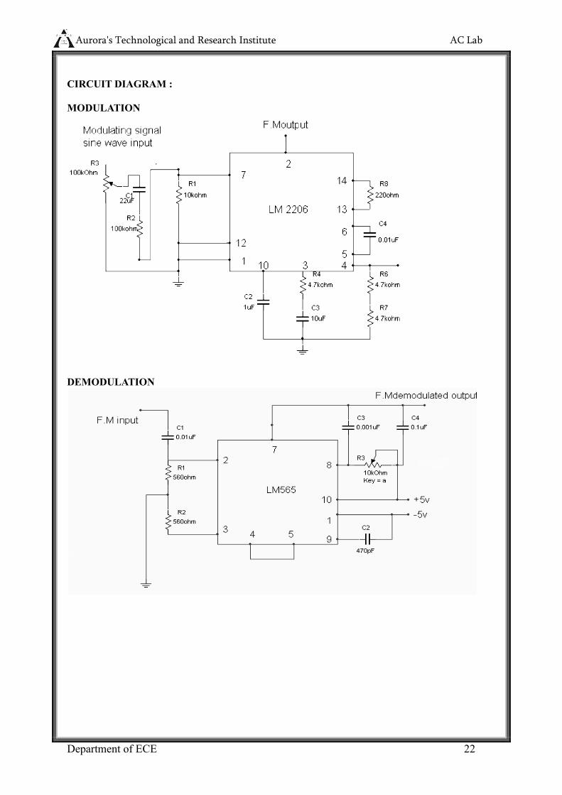
Auroras Technological and Research Institute AC Lab
Department of ECE 25
EXPERIMENT NO 5
STUDY OF SPECTRUM ANALIZER AND ANALYSIS OF AM amp FM SIGNALS
Auroras Technological and Research Institute AC Lab
Department of ECE 26
Auroras Technological and Research Institute AC Lab
Department of ECE 27
Auroras Technological and Research Institute AC Lab
Department of ECE 28
EXPERIMENT NO 6
PRE EMPHASIS AND DE EMPHASIS
OBJECTIVE To study the operation of Pre-emphasis and De-emphasis circuits
PRE-LAB
1 Study the theory of Pre-emphasis and De-emphasis circuits
2 Draw the circuit diagram
3 Draw the expected waveforms
COMPONENTS
1 Resistors 100kΩ 100Ω
2 Capacitors 1μf 100μf EQUIPMENT 1 Function generator 1
2 Dual trace CRO 1
THEORY Pre-emphasis
Improving the signal to noise ratio by increasing the magnitude of higher frequency
signals with respect to lower frequency signals
De-emphasis
Improving the signal to noise ratio by decreasing the magnitude of higher
frequency signals with respect to lower frequency signals
Transmitters that employ a true FM modulator require a pre emphasis circuit before the
modulator fore the true FM modulator doesnt automatically pre emphasize the audio like
a transmitter that uses a phase modulator A separate circuit is not necessary for pre
emphasis in a transmitter that has a phase modulator because the phase modulator applies
pre emphasis to the transmitted audio as a function of the phase modulator The receivers
De emphasis circuitry takes the unnatural sounding pre emphasized audio and turns it
back into its original response Pre emphasized (discriminator) audio is however available
directly from the audio demodulation (discriminator) circuitry In linking systems many
choose to eliminate the emphasis circuitry to allow better representation of retransmitted
Auroras Technological and Research Institute AC Lab
Department of ECE 29
signals Since the signal has already been pre emphasized (by the user that is
transmitting) and since the receiver you are listening to takes care of the de emphasis
CIRCUIT DIAGRAMS
PRE-EMPHASIS
DE-EMPHASIS
EXPECTED WAVEFORMS
INPUT
TIME T
A
m
p
l i t u
d
e
Am
Auroras Technological and Research Institute AC Lab
Department of ECE 30
OUTPUT
PRE-EMPHASIS
Freq Vs Gain
DE-EMPHASIS
Freq Vs Gain
TIME T
Freq f (Hz)
A
m
p
l i t u
d
e
Am
Auroras Technological and Research Institute AC Lab
Department of ECE 31
TABLE
PRE EMPHASIS
SNo Input Freq
Input Voltage Vi (Volts)
Output Voltage Vo (Volts) Gain=VoVi
Gain in dB
20log(voVi)
DE-EMPHASIS
SNo Input Freq
Input Voltage Vi (Volts)
Output Voltage Vo (Volts)
Gain=VoVi Gain in dB
20log(VoVi)
PROCEDURE a Pre-emphasis
1 Connect the circuit as per the circuit diagram
2 Apply a constant sine wave input across the input terminal of fixed amplitude(Vi) 3 By varying the input frequency note down the output amplitude (Vo) with respect to
input frequency in Table 4 Calculate the gain using the formula
5 Gain =20log (Vo) (Vi) db
b De-Emphasis
1 Connect the circuit as per the circuit diagram
2 Repeat the steps 2 3 amp4
POST LAB
1 Observe the output amplitude for both the pre-emphasis and De-emphasis circuits
2 Calculate the gain in db
3 Plot the frequency versus gain curves on logarithmic graphs for both the circuits
4 Plot the input and output waveforms Time T VS Voltage Vo
5 Write the result and conclusion
CONCLUSIONS Obtained the pre emphasis and de-emphasis outputs
QUESTIONS 1 Observe the out put signal is disturbed by noise what action has to be taken and measure the
output voltage 2 Where we use the pre emphasis circuit 3 Where we use the de emphasis circuit 4 What are the advantages of pre emphasis and de emphasis circuits
Auroras Technological and Research Institute AC Lab
Department of ECE 32
EXPERIMENT NO 7
TIME DIVISION MULTIPLEXING AND DEMULTIPLEXING
AIM To study Time Division Multiplexing and its waveforms
PRE LAB WORK
Study the operation of Time division multiplexer and demultiplexer Draw the block diagram of TDM
Draw the expected graphs of all necessary waveforms ( CH1CH2TDM OP and Demultiplexed OP)
EQUIPMENT
1) Experimental board on TDM
2) Dual Trace CRO 3) Probes
THEORY
Time Division Multiplexing (TDM) is a technique for transmitting serial messages on a signal
transmission channel by dividing the time division into slots One slot for each message The concept
of TDM comes from sampling theorem which enables use to transmit the information contained in the
band limited Signal using sampling of the signal taken uniformly or a rate slightly higher then the
Nyquist rate TDM enables the joint utilization at a common transmission channel by a number of
independent message sources without mutual interference
The different Ip message signals all band limited in WHz by the IP low pass filters and sequentially
sampled at the transmitters by a rotary switch or a comparator The switch makes are complete
revolution in Ts frac12 W extracting are sample from each IP The commutator OP is a PAM waveform
containing individual message sample
It there are N number of IP the pulse to Pulse spacing will be Ts = 1 while the spacing
N Nfs
bw successive samples from each IP is called a frame
At the receiver a similar rotatory switch the decommutator separates the samples and distributes them
to a bank of low-pass filters which in turn is usually electronic and synchronization signals are
provided to keep the distribute in step with the commutant
Auroras Technological and Research Institute AC Lab
Department of ECE 33
EXPECTED GRAPHS
PROCUDURE
1 Connect the OP of the experimental board to one of the channels on CRO 2 Switch ON the experimental board 3 Observe the OP waveforms 4 Vary the values of the resistors R1 R2 and R3 alternative and observe the OP on CRO
RESULT
The process of the Time Division Multiplexing and the waveforms has been studied
CONCLUSION
Auroras Technological and Research Institute AC Lab
Department of ECE 34
Figure 1 Time Division Multiplexing amp De multiplexing
Auroras Technological and Research Institute AC Lab
Department of ECE 35
EXPERIMENT NO 9
VERIFICATION OF SAMPLING THEOREM
AIM To study the effect of sampling on the transmission of information through PWM
PRE LAB WORK
Study the sampling theorem
Draw the expected graphs of all necessary waveforms ( message signal carrier wave PWM op demodulated op etc
EQUIPMENT
1) Experimental Board on study of sampling theorem 2) Dual trace CRO (0 ndash 20 MHz) 3) Function Generator 4) Connecting wires
THEORY
The principle of sampling can be explained using the switching sampler The switch periodically shifts below bw two constants at the rate of fs = 1 Ts Hz staying on the IP constant for each sampling period The op Xs(t) of the samples consists of segments of x(t) and Xc(t) can be represented as
Xs(t) = X(t) S(t)
Where S(t) is sampling or switching function There are a number of differences bw the ideal sampling and reconstruction techniques described in the proceeding sections of the actual signal
PROCEDURE
1) Observe the internal clock and measure its frequency and amplitude 2) Give the clock to the clock IP terminal 3) Connect the modulating signal to the IP 4) Check the condition fs gt 2fm and observe the de-modulated wave 5) Check the condition fs lt 2fm and fs = 2fm and draw the OP waveforms
RESULT
CONCLUSION
Aurorarsquos Technological and Research Institute DC Lab
36
Figure 2 Sampling Theorem
Aurorarsquos Technological and Research Institute DC Lab
37
EXPERIMENT NO 10
PULSE AMPLITUDE MODULATION AND DEMODULATION
AIM 1) To study the PAM modulation and its waveforms
2) To study the de-modular of PAM
3) To study the effect of sampling frequency on de-modulation OP
PRE LAB WORK
Study the operation Pulse Amplitude Modulator and Demodulator Draw the block diagram of PAM modulator and demodulator Draw the expected graphs of all necessary waveforms ( message signal carrier wave PAM op
demodulated op etc)
EQUIPMENT
1) Exp Board on study of PAM 2) CRO 3) Functional Generator 4) Connecting wires and chords
THEORY
In PAM the amplitude of the carrier wave of higher frequency follow the amp of the message signal
Within this (Modulation Sampling) we have two more types of sampling those are
(1) Natural Sampling
(2) Flat Top Sampling
Basically in Natural Sampling the carrier waves are train of pulses of a certain frequency After
sampling the top of the Pulse follow the message signal Due to this following of top of Pulses with the
message signals cause a distortion in De-modulation
In Flat top sampling also we use train of pulses for sampling but only the starting point of each pulse
follow the message signal remaining width of the pulse will (follow) be flat But here we go for Natural
sampling
EXPECTED WAVEFORMS
Aurorarsquos Technological and Research Institute DC Lab
38
PROCEDURE (MODULATION)
1 Observe the clock on CRO and measure its frequency and amp (freq 5KHz) 2 Connect the clock to clock IP terminals in modulation 3 Put control switch in ac position and set amplitude = OV This provides DC at Modulating
signal terminal 4 Connect the modulating signal or IP to the modulator 5 Connect one channel of CRO at lsquoTirsquo and Gnd Observe that the pulses are of same height
Height is adjustable by varying offset This is PAM signal with DC IP Measure amplitude and frequency of Pulses
6 Increase the amplitude of modulation signal Observe the amplitude and frequency of this sinusoidal modulating signal
7 Observe PAM signal
a) How many Pulses are there in one modulating cycle
b) It is natural or Flat Top PAM c) It is Single or dual polarity PAM
8 Observe the effect of DC offset on PAM waveform
DE-MODULATION
1) Generate undistorted PAM waveform 2) Connect the modulating signal to de-modulation IP 3) Observe the detected OP and measure its frequency which must be same as
modulating signal
EFFECT OF SAMPLING FREQUENCY
1) Connect internal sinusoidal signal to modulating signal IP of the modulator 2) Connect an external functional Generator at the circuit terminals of the modulator 3) Get the PAM waveform using the above circuit 4) Adjust the modulating amplitude offset and frequency to get an undistorted frequency 5) Connect the PAM to de-modulator IP 6) Observe the demodulated signal for various frequencies of clock (fs gt 2fm lt 2fm = 2 fm)
RESULT
CONCLUSION
Aurorarsquos Technological and Research Institute DC Lab
39
Figure 3 Pulse Amplitude Modulation
Auroras Technological and Research Institute AC Lab
Department of ECE 5
EXPERIMENT NO 11
PULSE WIDTH MODULATION AND DEMODULATION
AIM
1) To study the PWM process and the corresponding waveforms 2) To study the effect of sampling frequency on the transmission of information through PWM
PRE LAB WORK
Study the operation Pulse Width Modulator and Demodulator Draw the block diagram of PWM modulator and demodulator Draw the expected graphs of all necessary waveforms ( message signal carrier wave PWM op
demodulated op etc
EQUIPMENT
1) Experimental Board
2) Dual trace CRO 3) AF generator 4) Multimeter
THEORY
In PWM the samples of the message signal are used to vary the duration of the individual pulses The
pulse width may be varied by varying the time of occurrence of the leading edge trailing edge of both
edges of the pulse in accordance with the sampled value of the modulating wave PWM can also be
generated by using emitter follower monostable multivibrator is an excellent voltage to time converter
since its gate width is dependent on the voltage to which the capacitor is changed If this voltage can be
varied in accordance with a signal voltage a series of rectangular pulses can be obtained with width
varying as required
The demodulated of PWM is quite simple PWM is passed through a low pass filter The reconstruction is
associated with a certain amount of Distortion caused by the cross modulator products that fall in the
signal band
EXPECTED WAVEFORM
Aurorarsquos Technological and Research Institute DC Lab
41
PROCEDURE
STUDY OF MODULATION
1) Observe the clock on CRO and measure its frequency (fs) 2) Observe the sine wave modulating signal on CRO and observe the dc shift produced in this
by varying the offset nob Measure the frequency Variation limits of this signal 3) Apply clock at the circuit input terminal 4) Apply modulating signal by keeping the control switch in dc position 5) Observe the modulated wave 6) Plot the graph bw pulse width and the applied dc voltage 7) Put the control switch in sine wave position and adjust the modulating signal amplitude
frequency and dc offset to get the stationary waveform of PWM 8) Note the number of pulses in one circuit of modulating signal
STUDY OF DEMODULATION
1) Generate the stationary PWM waveform using sin wave modulating signal 2) Connect the modulator OP to PWM demodulator 3) Connect Channel (1) to Modulating Signal and channel (2) to demodulated wave
EFFECT OF SAMPLING FREQUENCY
1) Use an external square wave and connect it to the clock input 2) Set the frequency of square wave at frequency 2fm 3) Observe the demodulated wave
4) Change the frequency of square wave to fs lt 2fm fs gt 2fm and observe the demodulated wave
RESULT
CONCLUSION
Aurorarsquos Technological and Research Institute DC Lab
42
Figure 4 Pulse Width Modulation
Aurorarsquos Technological and Research Institute DC Lab
43
EXPERIMENT NO 12
PULSE POSITION MODULATION AND DEMODULATION
AIM
1) To study the PPM Modulation and the corresponding waveforms 2) To study the de-modulation of PPM 3) To see the effect of sampling frequency on the transmission of information through PPM
PRE LAB WORK
Study the operation Pulse Position Modulator and Demodulator Draw the block diagram of PPM modulator and demodulator Draw the expected graphs of all necessary waveforms ( message signal carrier wave PPM op
demodulated op etc
EQUIPMENT
1) Experimental Board for PPM
2) Dual Phase Oscilloscope
3) AF Generator
THEORY
In PDM long pulses expand considerable power duration If the pulse which bearing no additional
information If this un used power is subtracted from PDM so that only time transitions are preserved
We observe a more efficient type of pulse modulation known as pulse position modulation Here in the
Pulse Position Modulated wave the position of the Pulse relative to its unmodulated time of occurrence is
varied in accordance with the message signal
We generate a PPM wave from PWM wave by using a Monostable Multivibrator The device has one
absolutely stable state and one quest ndash stable state into which it is triggered by an externally applied Pulse
The monostable multivibrator is designed to trigger on the trailing edges of the duration ndash modulated pulse
is varied in accordance with the message signal
The fixed pulse duration of the PPM wave at the monostable multivibrator OP can be set by appropriately
choosing the resistance ndash capacitance combination in the timing circuit of the device
Aurorarsquos Technological and Research Institute DC Lab
44
EXPECTED WAVEFORM
PROCEDURE
STUDY OF MODULATION
Observe the clock and measure its frequency (fs) Apply the clock at the clock IP terminal in the modulator Apply the modulating signal keeping control switch in DC position Observe the PPM OP Connect the channel ndash (1) on CRO to clock and channel (2) to PPM wave OP Compare the position of two waveforms Vary the DC offset and observe the relative shift between the clock and PPM OP Measure the time shift between clock and PPM wave for various settings of offset Draw the graph between time shift and DC voltage Put the control switch in AC position adjusts the amplitude and frequency and offset
of sinusoidal modulating signal to get the stationary PPM wave Note the number of pulses in one cycle of the modulated wave
STUDY OF DEMODULATION
Generate a stationery PPM wave for a sinusoidal modulating signal Apply the PPM wave to the input of de-modulator Connect the Channel ndash (1) of CRO to the modulating signal and channel ndash 2 to the
de-modulator output Compare the two waveforms
Note the frequency of demodulated wave It should be same as the modulating signal Note down the waveform
RESULT
CONCLUSION
Aurorarsquos Technological and Research Institute DC Lab
45
Aurorarsquos Technological and Research Institute DC Lab
46
Figure 5 Pulse Position Modulation
Aurorarsquos Technological and Research Institute AC Lab
47
EXPERIMENT NO 13
FREQUENCY SYNTHESIZER
AIM
To study the operation of frequency synthesizer using PLL
PRE-LAB 1 Study the data sheet of IC 7404IC 4017IC 565 and IC 4046
2 Study the theory of frequency synthesizer 3 Draw the circuit diagram and expected waveforms
EQUIPMENTS
1 Frequency synthesizer trainer AET -26A
2 Dual trace CRO (20Mhz) 3 Digital frequency counter or multimeter
4 Patch chords
THEORY
A frequency synthesizer is an electronic system for generating any of a range
of frequencies from a single fixed time base or oscillator They are found in many modern
devices including radio receivers mobile telephones radiotelephones walkie-talkies CB
radios satellite receivers GPS systems etc A frequency synthesizer can combine
frequency multiplication frequency division and frequency mixing (the frequency mixing
process generates sum and difference frequencies) operations to produce the desired output
signal
BLOCK DIAGRAM
Phase Comparator
Amplifier Low pass filter
V C O
Div N Network frequency divider
Fin= fout
N
fin
Fout =Nf in
Aurorarsquos Technological and Research Institute AC Lab
48
SIMPLE 1KHZ-9KHZ FREQUENCY SYNTHESIZER
CIRCUIT DAIGRAM
PROCEDURE 1 Switch on the trainer ad verify the output of the regulated power supply ie 5V These
supplied are internally connected to the circuit so no extra connections are required 2 Observe output of the square wave generator using oscilloscope and measure the range
with the help of frequency counter frequency range should be around 1KHz to 10KHz 3 Calculate the free running frequency range of the circuit (VCO output between 4th pin
and ground 1 For different values of timing resistor R1 ( to measure Rt value using digital multimeter between given test points 1 And record the frequency values in table 1
Fout = 03 (RtCt) where Rt is the timing resistor and Ct is the timing capacitor = 001 f
Aurorarsquos Technological and Research Institute AC Lab
49
4 Connect 4th pin of LM 565 (Fout) to the driver stage and 5th pin (Phase comparator) connected to 11th pin of 7404 Output can be taken at the 11th pin of the 7490 It should be divided by the 2 amp 3 times of the fout
TABULATION
Fin KHz Fout = N x fin KHz Divided by 3 2
EXPECTED WAVEFORMS
POST LAB
1 Observe the synthesized output in table 2 Calculate the output frequency
3 Plot the output waveforms
4 Write result and conclusions
CONCLUSIONS
The various outputs of frequency synthesizer are verified
QUESTIONS
1 What are the applications of frequency synthesizer
TIME T
A
m
p
l i T
u
d
e
Ac
Aurorarsquos Technological and Research Institute AC Lab
50
2 What is the difference between heterodyning and synthesizer
Aurorarsquos Technological and Research Institute AC Lab
51
EXPERIMENT NO 14
AGC CHARATERISTICS
AIM
To observe the effect of automatic gain control(AGC)
PRE LAB 1 To study the theory of AGC 2 Draw the Block Diagram circuits diagram and expected waveforms
EQUIPMENTS 1 AGC Trainer Kit 2 CRO
3 Patch Chords
4 Digital Multimeter
THEORY
Automatic gain control (AGC) is an adaptive system found in many electronic
devices The average output signal level is fed back to adjust the gain to an appropriate level
for a range of input signal levels For example without AGC the sound emitted from an AM
radio receiver would vary to an extreme extent from a weak to a strong signal the AGC
effectively reduces the volume if the signal is strong and raises it when it is weaker AGC
algorithms often use a PID controller where the P term is driven by the error between
expected and actual output amplitude
Block Diagram
Frequency Converter
1st IF Amplifier
2nd IF Amplifier
Detector
Audio Preamplifier
Driver Output
Aurorarsquos Technological and Research Institute AC Lab
52
CIRCUIT DIAGRAM
PROCEDURE
1 Connect 455 KHz IF Signal Function Generator connect AGC link Connect CRO channel-1 at input terminals
2 Connect CRO channel 2 at collector of Q3 The amplified signal will be observed 3 Calculate the voltage gain by measuring the amplitude of output signal (Vo) waveform
using formula A=VoVi 4 Now connect CRO-2 channel at output The detected audio signal of 455 Khz will be
observed 5 Now vary input level of 455 KHz IF signal and observe detected 455 KHz audio signal
with and without AGC link The output will be distorted when AGC link is removed ie there is no AGC action
6 This explains AGC effect in Radio circuit
TABULATION
SNo Input Voltage Vi (P-P) With out AGC With AGC
Output Voltage Vo (P-P)
Gain A= Vo Vi
Output Voltage Vrsquoo (P-P)
Gain Arsquo= Vrsquoo Vi
Aurorarsquos Technological and Research Institute AC Lab
53
EXPECTED WAVEFORMS
AM Modulated RF Input
Detected Output with AGC
Detected Output without AGC
POST-LAB
1 Observe the input voltage and output voltage for with AGC and Without AGC in Table 1
2 Calculate Gain a=vovi for both cases 3 Plot the output waveforms Time T Vs Voltage Vo and input voltage Vi Vs Gain A 4 Write Result and Conclusions
CONCLUSIONS The AGC characteristics are verified
QUESTIONS 1 what is meant by AGC
2 What is the difference between simple AGC and delayed AGC
3 From which part of receiver AGC is obtained
TIME T
A
m
p
l i T
u
d
e
Ac
TIME T
A
m
p
l i T
u
d
e
Ac
TIME T
A
m
p
l i T
u
d
e
Ac
Aurorarsquos Technological and Research Institute AC Lab
54
EXPERIMENT NO 15
PHASE LOCKED LOOP
OBJECTIVE To study the Phase locked loop using 565 IC and to take input frequency given by an external signal source
PRE-LAB To Study
1 The data sheet of IC 565
2 The theory of Phase locked loop
3 About free running frequency locking range and capture range
4 Draw the circuit diagram and expected waveforms
EQUIPMENT 1 Function generator 2
2 Dual trace CRO 1
3 Phase locked loop trainer kit
THEORY
A phase-locked loop or phase lock loop (PLL) is a control system that generates a signal
that has a fixed relation to the phase of a reference signal A phase-locked loop circuit
responds to both the frequency and the phase of the input signals automatically raising or
lowering the frequency of a controlled oscillator until it is matched to the reference in both
frequency and phase A phase-locked loop is an example of a control system using negative
feedback Phase-locked loops are widely used in radio telecommunications computers and
other electronic applications They may generate stable frequencies recover a signal from a
noisy communication channel or distribute clock timing pulses in digital logic designs
such as microprocessors Since a single integrated circuit can provide a complete phase-
locked-loop building block the technique is widely used in modern electronic devices
with output frequencies from a fraction of a cycle per second up to many gigahertz
BLOCK DIAGRAM
Aurorarsquos Technological and Research Institute AC Lab
55
CIRCUIT DIAGRAM
PROCEDURE 1 Switch ON the trainer kit 2 Check the VCO output at pin 4 of IC 565 that is a square wave form The frequency of the
VCO Output depends on CT (001f) and RT (47kΩ) 3 Next short the pins 4amp5 and give signal of variable frequency and observe VCO output 4 Change the input frequency and observe the VCO output on the CRO 5 Between some frequencies the VCO output is locked to the input signal frequency This can
be observed by increasing or decreasing the frequency of the VCO output by changing input frequency
6 Before or after that frequency range the VCO output is not locked
7 Calculate Lock range (FL) and capture range (FC) by using the following formulas
FL = 8foVCO fo=03RtCT
FC=12π radic2πf236103 C2
Table1
SNo Locking Frequency Frequency Range From To
CHARTERISTICES
Aurorarsquos Technological and Research Institute AC Lab
56
CONCLUSIONS Obtained the lock range of PLL
QUESTIONS
1 Observe the VCO output when pins 4amp5 short and give square wave as signal 2 Define lock range and capture range
3 What are the basic applications of PLL
Aurorarsquos Technological and Research Institute AC Lab
57
ANNEXURE-I
EXPERIMENT NO 1
Aurorarsquos Technological and Research Institute AC Lab
58
CHARACTERISTICS OF MIXER
AIM
To study the functioning of a frequency mixer
PRE LAB 1 To study the theory of Mixer 2 Draw the circuit diagram and expected waveforms
EQUIPMENTS 1 Frequency mixer trainer kit 2 CRO (20MHz) 3 Connecting cords and probes 4 Function generator (1MHz)
THEORY
In receivers using the super heterodyne principle a signal at variable frequency is
converted to a fixed lower frequency IF before detection IF is called the intermediate frequency
In typical AM (Amplitude Modulation eg as used on medium wave) home receivers that
frequency is usually 455 kHz for FM VHF receivers it is usually 107 MHz An intermediate
frequency (IF) is a frequency to which a carrier frequency is shifted as an intermediate step in
transmission or reception Frequency modulation (FM) is a form of modulation that represents
information as variations in the instantaneous frequency of a carrier wave Very high frequency
(VHF) is the radio frequency range from 30 MHz (wavelength 10 m) to 300 MHz (wavelength 1
heterodyne receivers mix all of the incoming signals with an internally generated waveform
called the local oscillator The user tunes the radio by adjusting the sets oscillator frequency in
the mixer stage of a receiver the local oscillator signal multiplies with the incoming signals
which shifts them all down in frequency The one that shifts is passed on by tuned circuits
amplified and then demodulated to recover the original audio signal The oscillator also shifts a
copy of each incoming signal up in frequency by amount Those very high frequency images
are all rejected by the tuned circuits in the IF stage The Super heterodyne receiver (or to give it its
full name The Supersonic Heterodyne Receiver usually these days shortened to superhet) was
invented by Edwin Armstrong in 1918
Aurorarsquos Technological and Research Institute AC Lab
59
BLOCK DIAGRAM
CIRCUIT DIAGRAM
EXPECTED WAVEFORMS
INPUT SIGNAL Fx
INPUT SIGNAL Fy
TIME T
A
m
p
l i T
u
d
e
Ac
Aurorarsquos Technological and Research Institute AC Lab
60
MIXER OUTPUT(Fy-Fx)
PROCEDURE 1 Connect the circuit as per the given circuit diagram 2 Switch on the power supply of trainer kit 3 Apply a sine wave at input Fx of 2 VP-P amplitude and 100 KHz frequency 4 Apply a sine wave at input FY of 2 VP-P amplitude and 100 KHz frequency 5 Observe the output waveform on the CRO 6 Repeat the steps 34 and 5 by changing the values of Fx once greater than and less than
FY in a steps of 5Khz (in the range 80KHz to 120KHz)
TABULATION
TIME T
A
M
P
L
I T
U
D
E
TIME T
A
m
p
l i T
u
d
e
Ac
Aurorarsquos Technological and Research Institute AC Lab
61
SNo Freq (Fy)
(kHz) Amp(V) Freq(Fx) (kHz) Amp(V) Freq(Fy-Fx)
(kHz) Amp(V)
POST LAB 1 Observe the amplitude and time Of inputs and output in table
2 Draw the expected waveforms
3 Verify the output signal obtained with the theoretical value 4 Plot the graphs for Time T VS input signal (FX) Voltage V input signal (FY) Voltage V
and output Signal F(x-y) voltage V 5 Write result and conclusions
CONCLUSIONS
Obtained the output of the mixer for various inputs
QUESTIONS
1 what are the different types of mixtures available
2 What is meant by heterodyning
3 What is meant by IF
Aurorarsquos Technological and Research Institute AC Lab
62
EXPERIMENT NO 2
DIGITAL PHASE DETECTOR
OBJECTIVE To detect the phase difference between two square wave signals using digital phase detector
PRE LAB
1 To study the theory of digital phase detector and EX-OR gate operation and truth table 2 Draw the circuit diagram and expected output and input waveforms
EQUIPMENT 1 Digital phase detector trainer kit 2 Regulated power supplies
3 CRO (20MHz) 4 Connecting cords amp probes
5 Digital frequency counter or multimeter
THEORY
Phase detector is a frequency mixer or analog multiplier circuit that generates a voltage
signal which represents the difference in phase between two signal inputs It is an essential
element of the phase-locked loop (PLL)Detecting phase differences is very important in many
applications such as motor control radar and telecommunication systems servo mechanisms and
demodulators
Electronic phase detector
Some signal processing techniques such as those used in radar may require both the amplitude
and the phase of a signal to recover all the information encoded in that signal One technique is to
feed an amplitude-limited signal into one port of a product detector and a reference signal into the
other port the output of the detector will represent the phase difference between the signals If the
signal is different in frequency from the reference the detector output will be periodic at the
difference frequency Phase detectors for phase-locked loop circuits may be classified in two
types A Type I detector is designed to be driven by analog signals or square-wave digital signals
and produces an output pulse at the difference frequency The Type I detector always produces an
output waveform which must be filtered to control the phase-locked loop variable frequency
oscillator (VCO) A type II detector is sensitive only to the relative timing of the edges of the input
and reference pulses and produces a constant output proportional to phase difference when both
signals are at the same frequency This output will tend not to produce ripple in the control voltage
of the VCO
Aurorarsquos Technological and Research Institute AC Lab
63
BLOCK DIAGRAM OF PLL
CIRCUIT DIAGRAM
Aurorarsquos Technological and Research Institute AC Lab
64
EXPECTED WAVEFORMS
EX-OR PHASE DETECTOR
EDGE TRIGGERED OUTPUT
PROCEDURE
1 Switch on the trainer kit
2 Observe the output of the square wave generator available on the trainer kit using CRO
and measure the range with the help of frequency counter the frequency range should be
around 2 KHz to 13 KHz
3 Calculate the free running range of the VCO output ie between 4th pin of IC PLL 565
and ground For different values of timing resistor Rt fout is given by Fout =03 Rt Ct
where Ct timing capacitor = 001 μF Rt timing resistor
4 Connect the square wave to the input of IC PLL 565 and short 4th and 5th pin of PLL
Vary the input frequency of the square wave when the PLL is locked that is connected to
Aurorarsquos Technological and Research Institute AC Lab
65
one input fout EX-OR phase detector The other input fin of EX-OR phase detector is the
coming from inbuilt of square wave generator
5 Connect the pulse generator output to the input of IC 565 PLL and short 4th amp 5th pin of
PLL Vary the input frequency of the square wave when the PLL is locked that is
connected to one input of Edge triggered phase detector input ie fout The other input fin
of edge triggered phase detector is the pulse input coming from the inbuilt pulse generator
6 The dc output voltage of the exclusive-OR phase detector is a function of the phase
difference between its two inputs fin and fout
POST LAB
1 Observe the Voltage and Time of the two input square waves
2 Observe difference of two inputs as square wave output
3 Plot the inputs and output waveforms Time T VS Voltage V
CONCLUSIONS
The phase detector outputs are verified
QUESTIONS
1 What is the function of phase detector
2 What is the condition for getting maximum output
3 Advantages of digital phase detector over analog phase detector
Aurorarsquos Technological and Research Institute AC Lab
66
EXPERIMENT NO 3
COASTAS RECEIVER
AIM
To demodulate a DSB-SC signal using coastas receiver
PRE LAB 1 To study the operation of coastas receiver 2 Draw the circuit diagram and expected waveforms
EQUIPMENTS 1 Communications trainer kit 2 DSB-SC modulator trainer kit 3 CRO (20MHz) 4 Connecting cords and probes 5 Function generator (1MHz)
THEORY
This loop and its variations is much-used as a method of carrier acquisition (and
simultaneous message demodulation) in communication systems both analog and digital
It has the property of being able to derive a carrier from the received signal even when there is
no component at carrier frequency present in that signal (eg DSBSC) The requirement is that
the amplitude spectrum of the received signal be symmetrical about this frequency
The Costas loop is based on a pair of quadrature modulators - two multipliers
fed with carriers in phase-quadrature These multipliers are in the in-phase (I) and quadrature
phase (Q) arms of the arrangement Each of these multipliers is part of separate synchronous
demodulators The outputs of the modulators after filtering are multiplied together in a third
multiplier and the lowpass components in this product are used to adjust the phase of the local
carrier source - a VCO - with respect to the received signal The operation is such as to
maximise the output of the I arm and minimize that from the Q arm The output of the I arm
happens to be the message and so the Costas loop not only acquires the carrier but is a
(synchronous) demodulator as well A complete analysis of this loop is non-trivial It would
include the determination of conditions for stability and parameters such as lock range capture
range and so on
Aurorarsquos Technological and Research Institute AC Lab
67
BLOCK DIAGRAM
EXPECTED WAVEFORMS
DSB-SC modulated output
Aurorarsquos Technological and Research Institute AC Lab
68
Demodulated output of the coastas loop
PROCEDURE
1 Switch ON the DSB-SC trainer kit
2 Generate the carrier and modulating signal
3 Generate the DSB-SC modulated signal
4 Connect the required blocks of the coastas receiver in the communications kit
5 Apply the generated DSB-SC signal to the above connected coastas receiver
6 Observe that the output of the coastas receiver is the demodulated wave of DSB-SC signal
POST LAB
1 Observe the frequency and amplitude of the carrier and modulating signal
2 Observe the frequency and amplitude of the balanced modulator output
3 Observe the lock condition of the coastas loop
4 observe the output of the coastas demodulator
5 Write result and conclusions
CONCLUSIONS The balanced modulator output and the operation of coastas receiver is verified
QUESTIONS 1 what is the operation of coastas loop
2 What happens when the locking condition of the coastas loop occurs
3 Coastas loop can be used for demodulation of other modulation techniques also What are they
Aurorarsquos Technological and Research Institute AC Lab
69
MATLAB PROGRAMMES
Aurorarsquos Technological and Research Institute AC Lab
70
INDEX
1 Introduction - 70
2 Amplitude Modulation and Demodulation - 74
3 DSB-SC Modulation and Demodulation - 84
4 SSB-SC Modulation and Demodulation - 89
5 Frequency Modulation and Demodulation - 95
6 Phase Modulation and Demodulation - 99
7 Time Division Multiplexing and Demultiplexing - 100
8 Frequency Division Multiplexing and Demultiplexing- 103
9 Verification of Sampling Theorem - 104
10 Pulse Amplitude Modulation and Demodulation - 106
11 Pulse width Modulation and Demodulation - 108
12 Pulse Position Modulation and Demodulation - 110
13 PLL as FM Demodulator - 112
Aurorarsquos Technological and Research Institute AC Lab
71
1 INTRODUCTION
What Is Simulink
Simulink is a software package for modeling simulating and analyzing dynamic
systems It supports linear and nonlinear systems modeled in continuous time sampled time
or a hybrid of the two Systems can also be multirate ie have different parts that are
sampled or updated at different rates
Tool for Simulation
Simulink encourages you to try things out You can easily build models from scratch
or take an existing model and add to it You have instant access to all the analysis tools in
MATLABreg so you can take the results and analyze and visualize them A goal of Simulink
is to give you a sense of the fun of modeling and simulation through an environment that
encourages you to pose a question model it and see what happens
Simulink is also practical With thousands of engineers around the world using it to
model and solve real problems knowledge of this tool will serve you well throughout your
professional career
Tool for Model-Based Design
With Simulink you can move beyond idealized linear models to explore more realistic
nonlinear models factoring in friction air resistance gear slippage hard stops and the other
things that describe real-world phenomena Simulink turns your computer into a lab for
modeling and analyzing systems that simply wouldnt be possible or practical otherwise
whether the behavior of an automotive clutch system the flutter of an airplane wing the
dynamics of a predator-prey model or the effect of the monetary supply on the economy
For modeling Simulink provides a graphical user interface (GUI) for building models
as block diagrams using click-and-drag mouse operations With this interface you can draw
the models just as you would with pencil and paper (or as most textbooks depict them) This
is a far cry from previous simulation packages that require you to formulate differential
equations and difference equations in a language or program Simulink includes a
comprehensive block library of sinks sources linear and nonlinear components and
connectors You can also customize and create your own blocks For information on creating
your own blocks see the separate Writing S-Functions guide
Models are hierarchical so you can build models using both top-down and bottom-up
approaches You can view the system at a high level then double-click blocks to go down
through the levels to see increasing levels of model detail This approach provides insight into
how a model is organized and how its parts interact
After you define a model you can simulate it using a choice of integration methods either
from the Simulink menus or by entering commands in the MATLAB Command Window The
menus are particularly convenient for interactive work while the command-line approach is
very useful for running a batch of simulations (for example if you are doing Monte Carlo
simulations or want to sweep a parameter across a range of values) Using scopes and other
display blocks you can see the simulation results while the simulation is running In addition
Aurorarsquos Technological and Research Institute AC Lab
72
you can change many parameters and see what happens for what if exploration The
simulation results can be put in the MATLAB workspace for post processing and
visualization
Model analysis tools include linearization and trimming tools which can be accessed
from the MATLAB command line plus the many tools in MATLAB and its application
toolboxes And because MATLAB and Simulink are integrated you can simulate analyze
and revise your models in either environment at any point
1 Generation of cosine wave in time domain and frequency
domain Clc clear all close all x = -500015 t = 0140001 time = cos(23141000t) y1 = cos(23141000x) subplot(211) plot(xy1) axis([-5 5 -3 3]) grid on title(Time domain) xlabel(Time ) ylabel(Amplitude) now create a frequency vector for the x-axis and plot the magnitude and phase subplot(212) fre = abs(fft(time)) f = (0length(fre) - 1)4000length(fre) plot(ffre) grid on title(Frequency domain (Spectrum)) xlabel(Freq ) ylabel(Amplitude)
WAVEFORMS
Aurorarsquos Technological and Research Institute AC Lab
73
2 Generation of square wave in time domain and frequency
domain
clc clear all close all x = -500015 Fs = 399 t = 01Fs1 time = SQUARE(2pi1000t) y1 = SQUARE(23141000x) subplot(211) plot(xy1) axis([-5 5 -3 3]) grid on xlabel(Time domain) ylabel(Amplitude) now create a frequency vector for the x-axis and plot the magnitude and phase subplot(212) fre = abs(fft(time)) f = (0length(fre) - 1)Fslength(fre) plot(ffre) grid on xlabel(Freq domain) ylabel(Amplitude)
WAVEFORMS
Aurorarsquos Technological and Research Institute AC Lab
74
Aurorarsquos Technological and Research Institute AC Lab
75
2 AMPLITUDE MODULATION AND DEMODULATION PROGRAM 1
clc clear all close all Ac=1 Carrier Amplitude Fc=04 Carrier frequency Fm=005 baseband frequency Fs=10 sampling t=001200 mt=cos(2piFmt) under modulation mu=05 st=Ac(1+mumt)cos(2piFct) subplot(211) plot(tst) hold on plot(tAc(mumt+ones(1length(mt)))r) plot(t-Ac(mumt+ones(1length(mt)))r) hold off title(Modulation Index = 05 under modulation Ac(1+05cos(2pi005t))cos(2pi04t)) xlabel(time (s))ylabel(amplitude) st_fft=fft(st) st_fft=fftshift(st_fft) st_fft_fre=5linspace(-11length(st_fft)) subplot(212) plot(st_fft_freabs(st_fft)) title(spectrum with Modulation Index = 05) xlabel(Frequency (Hz))axis([-1 1 0 1000Ac+100])
total modulation figure mu=1 st=Ac(1+mumt)cos(2piFct) subplot(211) plot(tst) hold on plot(tAc(mumt+ones(1length(mt)))r) plot(t-Ac(mumt+ones(1length(mt)))r) hold off title(Modulation Index = 1 modulation Ac(1+1cos(2pi005t))cos(2pi04t)) xlabel(time (s))ylabel(amplitude) st_fft=fft(st) st_fft=fftshift(st_fft) st_fft_fre=Fs2linspace(-11length(st_fft)) subplot(212) plot(st_fft_freabs(st_fft)) title(spectrum with Modulation Index = 1) xlabel(Frequency (Hz))axis([-1 1 0 1000Ac+100])
Aurorarsquos Technological and Research Institute AC Lab
76
over Modulation figure mu=2 st=Ac(1+mumt)cos(2piFct) subplot(211) plot(tst) hold on plot(tAc(mumt+ones(1length(mt)))r) plot(t-Ac(mumt+ones(1length(mt)))r) hold offtitle(Modulation Index = 2 over modulation Ac(1+2cos(2pi005t))cos(2pi04t)) xlabel(time (s))ylabel(amplitude) st_fft=fft(st) st_fft=fftshift(st_fft) st_fft_fre=Fs2linspace(-11length(st_fft)) subplot(212) plot(st_fft_freabs(st_fft)) title(spectrum with Modulation Index = 2) xlabel(Frequency (Hz))axis([-1 1 0 1000Ac+100])
WAVEFORMS
Aurorarsquos Technological and Research Institute AC Lab
77
PROGRAM 2
Aurorarsquos Technological and Research Institute AC Lab
78
task 1 fc=154000
task 2 fm=fc10 fs=100fc t=01fs4fm xc=cos(2pifct) xm=cos(2pifmt) figure(1) subplot(211)plot(txc) title(carrier signal of 154 khz) xlabel(time (sec)) ylabel(amplitude) subplot(212)plot(txm) title(message signal of 154 khz) xlabel(time (sec)) ylabel(amplitude) DSB-SC MODULATION mu = input( enter the Modulation Index value ) z1=(1+muxm)xc figure(2)
task 31 subplot(211)plot(tz1) title(AMPLITUDE MODULATION IN TIME DAOMAIN) xlabel(time (sec)) ylabel(amplitude)
task 32 l1=length(z1) f=linspace(-fs2fs2l1) Z1=fftshift(fft(z1l1)l1) subplot(212)plot(fabs(Z1)) title(AMPLITUDE MODULATION IN FREQUENCY DOMAIN) xlabel(frequency(hz)) ylabel(amplitude) axis([-200000 200000 0 03])
task 33 demodulation s1=z1xc S1=fftshift(fft(s1length(s1))length(s1)) figure(3) plot(fabs(S1)) title( demodulated signal IN FREQUENCY DOMAIN before filtring) xlabel(frequency(hz)) ylabel(amplitude) axis([-200000 200000 0 03]) hold on Hlp=1sqrt(1+(ffc)^(2100)) plot(fHlpr) title( frequency response of low pass filter) xlabel(frequency(hz)) ylabel(amplitude) axis([-200000 200000 0 2])
task 34 E1=HlpS1 figure(4) subplot(211)plot(fE1)
Aurorarsquos Technological and Research Institute AC Lab
79
title( Recover signal IN FREQUENCY DOMAIN after filtring) xlabel(frequency(hz)) ylabel(amplitude) axis([-200000 200000 0 03]) e1=ifft(ifftshift(E1))length(E1) subplot(212)plot(t(105)e1) title( Recover signal IN Time DOMAIN after filtring) xlabel(time(sec)) ylabel(amplitude)
WAVEFORMS
enter the Modulation Index value 05
0 1 2 3
x 10-4
-1
-05
0
05
1carrier signal of 154 khz
time (sec)
am
plit
ude
0 1 2 3
x 10-4
-1
-05
0
05
1message signal of 154 khz
time (sec)
am
plit
ude
Aurorarsquos Technological and Research Institute AC Lab
80
0 1 2 3
x 10-4
-2
-1
0
1
2AMPLITUDE MODULATION IN TIME DAOMAIN
time (sec)
am
plit
ude
-2 -15 -1 -05 0 05 1 15 2
x 105
0
01
02
AMPLITUDE MODULATION IN FREQUENCY DOMAIN
frequency(hz)
am
plit
ude
-2 -15 -1 -05 0 05 1 15 2
x 105
0
02
04
06
08
1
12
14
16
18
2 frequency response of low pass filter
frequency(hz)
am
plit
ude
Aurorarsquos Technological and Research Institute AC Lab
81
enter the Modulation Index value 1
-2 -15 -1 -05 0 05 1 15 2
x 105
0
01
02
Recover signal IN FREQUENCY DOMAIN after filtring
frequency(hz)
am
plit
ude
0 1 2 3
x 10-4
05
1
15
2 Recover signal IN Time DOMAIN after filtring
time(sec)
am
plit
ude
0 1 2 3
x 10-4
-2
-1
0
1
2AMPLITUDE MODULATION IN TIME DAOMAIN
time (sec)
am
plit
ude
-2 -15 -1 -05 0 05 1 15 2
x 105
0
01
02
AMPLITUDE MODULATION IN FREQUENCY DOMAIN
frequency(hz)
am
plit
ude
Aurorarsquos Technological and Research Institute AC Lab
82
enter the Modulation Index value 2
-2 -15 -1 -05 0 05 1 15 2
x 105
0
02
04
06
08
1
12
14
16
18
2 frequency response of low pass filter
frequency(hz)
am
plit
ude
-2 -15 -1 -05 0 05 1 15 2
x 105
0
01
02
Recover signal IN FREQUENCY DOMAIN after filtring
frequency(hz)
am
plit
ude
0 1 2 3
x 10-4
0
1
2
3 Recover signal IN Time DOMAIN after filtring
time(sec)
am
plit
ude
Aurorarsquos Technological and Research Institute AC Lab
83
0 1 2 3
x 10-4
-4
-2
0
2
4AMPLITUDE MODULATION IN TIME DAOMAIN
time (sec)
am
plit
ude
-2 -15 -1 -05 0 05 1 15 2
x 105
0
01
02
AMPLITUDE MODULATION IN FREQUENCY DOMAIN
frequency(hz)
am
plit
ude
-2 -15 -1 -05 0 05 1 15 2
x 105
0
02
04
06
08
1
12
14
16
18
2 frequency response of low pass filter
frequency(hz)
am
plit
ude
Aurorarsquos Technological and Research Institute AC Lab
84
-2 -15 -1 -05 0 05 1 15 2
x 105
0
01
02
Recover signal IN FREQUENCY DOMAIN after filtring
frequency(hz)
am
plit
ude
0 1 2 3
x 10-4
-2
0
2
4 Recover signal IN Time DOMAIN after filtring
time(sec)
am
plit
ude
Aurorarsquos Technological and Research Institute AC Lab
85
3 DOUBLE SIDEBAND ndash SUPRESSED CARRIER MODULATION
AND DEMODULATION
PROGRAM 1 clc clear all close all Ts = 199 subplot(411) t = 01Ts1 m = cos(2pi1000t) plot(tm) title(Modulating Signal ) xlabel(Time) ylabel(Amplitude) grid on plot of the carrier signal
subplot(412) c = cos(2pi5000t) plot(tc) title(Carrier Signal ) xlabel(Time) ylabel(Amplitude) grid on plot of the DSB signal with Suppresed carrier intime domain
subplot(413) d = mc plot(td) title(DOUBLE SIDEBAND ndash SUPRESSED CARRIER SIGNAL ) xlabel(Time) ylabel(Amplitude) grid on freq domain of the DSB signal
subplot(414) fre = abs(fft(d)) f = (0length(fre) - 1)Tslength(fre) plot(ffre) axis([0 100 0 50]) grid on title(DOUBLE SIDEBAND ndash SUPRESSED CARRIER SPECTRUM ) xlabel(Freq domain) ylabel(Amplitude)
Aurorarsquos Technological and Research Institute AC Lab
86
WAVEFORMS
0 01 02 03 04 05 06 07 08 09 1-1
0
1Modulating Signal
Time
Am
plit
ude
0 01 02 03 04 05 06 07 08 09 1-1
0
1Carrier Signal
Time
Am
plit
ude
0 01 02 03 04 05 06 07 08 09 1-1
0
1DOUBLE SIDEBAND ndash SUPRESSED CARRIER SIGNAL
Time
Am
plit
ude
0 10 20 30 40 50 60 70 80 90 1000
50DOUBLE SIDEBAND ndash SUPRESSED CARRIER SPECTRUM
Freq domain
Am
plit
ude
Aurorarsquos Technological and Research Institute AC Lab
87
PROGRAM 2 task 1 fc=154000 task 2 fm=fc10 fs=100fc t=01fs4fm xc=cos(2pifct) xm=cos(2pifmt) figure(1) subplot(211)plot(txc) title(carrier signal of 154 khz) xlabel(time (sec)) ylabel(amplitude) subplot(212)plot(txm) title(message signal of 154 khz) xlabel(time (sec)) ylabel(amplitude) DSB-SC MODULATION z1= xmxc figure(2) task 31 subplot(211)plot(tz1) title(DSB-SC MODULATION IN TIME DAOMAIN) xlabel(time (sec)) ylabel(amplitude) task 32 l1=length(z1) f=linspace(-fs2fs2l1) Z1=fftshift(fft(z1l1)l1) subplot(212)plot(fabs(Z1)) title(DSB SC MODULATION IN FREQUENCY DOMAIN) xlabel(frequency(hz)) ylabel(amplitude) axis([-200000 200000 0 03]) task 33 demodulation s1=z1xc S1=fftshift(fft(s1length(s1))length(s1)) figure(3) plot(fabs(S1)) title( demodulated signal IN FREQUENCY DOMAIN before filtring) xlabel(frequency(hz)) ylabel(amplitude) axis([-200000 200000 0 03]) hold on Hlp=1sqrt(1+(ffc)^(2100)) plot(fHlpg) title( frequency response of low pass filter) xlabel(frequency(hz)) ylabel(amplitude) axis([-200000 200000 0 2]) task 34 E1=HlpS1 figure(4) subplot(211)plot(fE1) title( Recover signal IN FREQUENCY DOMAIN after filtring) xlabel(frequency(hz)) ylabel(amplitude) axis([-200000 200000 0 03]) e1=ifft(ifftshift(E1))length(E1) subplot(212)plot(t(105)e1)
Aurorarsquos Technological and Research Institute AC Lab
88
title( Recover signal IN Time DOMAIN after filtring) xlabel(time(sec)) ylabel(amplitude) WAVEFORMS
0 1 2 3
x 10-4
-1
-05
0
05
1carrier signal of 154 khz
time (sec)
ampl
itude
0 1 2 3
x 10-4
-1
-05
0
05
1message signal of 154 khz
time (sec)
ampl
itude
0 1 2 3
x 10-4
-1
-05
0
05
1DSB-SC MODULATION IN TIME DAOMAIN
time (sec)
ampl
itude
-2 -15 -1 -05 0 05 1 15 2
x 105
0
01
02
DSB SC MODULATION IN FREQUENCY DOMAIN
frequency(hz)
ampl
itude
Aurorarsquos Technological and Research Institute AC Lab
89
-2 -15 -1 -05 0 05 1 15 2
x 105
0
02
04
06
08
1
12
14
16
18
2 frequency response of low pass filter
frequency(hz)
ampl
itude
-2 -15 -1 -05 0 05 1 15 2
x 105
0
01
02
Recover signal IN FREQUENCY DOMAIN after filtring
frequency(hz)
am
plit
ude
0 1 2 3
x 10-4
-1
0
1
2 Recover signal IN Time DOMAIN after filtring
time(sec)
am
plit
ude
Aurorarsquos Technological and Research Institute AC Lab
90
4 SINGLE SIDE BAND - SUPRESSED CARRIER MODULATION AND DEMODULATION
PROGRAM 1
clc clear all close all Ts = 199 subplot(411) t = 01Ts1 xm = cos(2pi1000t) plot(txm) title(Modulating Signal ) xlabel(Time) ylabel(Amplitude) grid on plot of the carrier signal subplot(412) c = cos(2pi5000t) plot(tc) title(Carrier Signal ) xlabel(Time) ylabel(Amplitude) grid on subplot(413) helbert transform of messeage signal xh=cos((2pi1000t)-pi2) SSB UPPER SIDE BAND MODULATION d= (xmcos(2pi5000t))-(xhsin(2pi5000t)) plot(td) title(SINGLE SIDEBAND ndash SUPRESSED CARRIER SIGNAL ) xlabel(Time) ylabel(Amplitude) grid on freq domain of the DSB signal subplot(414) fre = abs(fft(d)) f = (0length(fre) - 1)Tslength(fre) plot(ffre) axis([0 100 0 50]) grid on title(SINGLE SIDEBAND ndash SUPRESSED CARRIER SPECTRUM ) xlabel(Freq domain) ylabel(Amplitude)
Aurorarsquos Technological and Research Institute AC Lab
91
WAVEFORMS
0 01 02 03 04 05 06 07 08 09 1-1
0
1Modulating Signal
Time
Am
plit
ude
0 01 02 03 04 05 06 07 08 09 1-1
0
1Carrier Signal
Time
Am
plit
ude
0 01 02 03 04 05 06 07 08 09 1-1
0
1SINGLE SIDEBAND ndash SUPRESSED CARRIER SIGNAL
Time
Am
plit
ude
0 10 20 30 40 50 60 70 80 90 1000
50SINGLE SIDEBAND ndash SUPRESSED CARRIER SPECTRUM
Freq domain
Am
plit
ude
Aurorarsquos Technological and Research Institute AC Lab
92
PROGRAM 2
task 1 fc=154000
task 2 fm=fc10 fs=100fc t=01fs4fm xc=cos(2pifct) xm=cos(2pifmt)
task 41 xh=cos((2pifmt)-pi2) helbert transform which is the phase shift of pi2 in messeage signal SSB UPPER SIDE BAND MODULATION z2= (xmcos(2pifct))-(xhsin(2pifct)) figure(5) subplot(211)plot(tz2) title(SSB USB MODULATION IN TIME DAOMAIN) xlabel(time (sec)) ylabel(amplitude) l2=length(z2) f=linspace(-fs2fs2l2) Z1=fftshift(fft(z2l2)l2) subplot(212)plot(fabs(Z1)) title(SSB USB MODULATION IN FREQUENCY DOMAIN) xlabel(frequency(hz)) ylabel(amplitude) axis([-400000 400000 0 1]) apply local carrier for demodulation z1= z2xc figure(6)
task 42 subplot(211)plot(tz1) title(DEMODULATED SSB in time domain) xlabel(time (sec)) ylabel(amplitude) l1=length(z1) f=linspace(-fs2fs2l1) Z1=fftshift(fft(z1l1)l1) subplot(212)plot(fabs(Z1)) title(DEMODULATED SSB IN FREQUENCY DOMIAN) xlabel(frequency(hz)) ylabel(amplitude) axis([-400000 400000 0 03])
task 43 figure(7) plot(fabs(Z1)) title(FILTERING SIGNAL) xlabel(frequency(hz)) ylabel(amplitude) hold on Hlp=1sqrt(1+(ffc)^(2100)) plot(fHlpg) title( frequency response of low pass filter) xlabel(frequency(hz)) ylabel(amplitude)
Aurorarsquos Technological and Research Institute AC Lab
93
axis([-400000 400000 0 2])
task 44 E1=HlpZ1 figure(8) subplot(211)plot(fE1) title( Recover signal IN FREQUENCY DOMAIN after filtring) xlabel(frequency(hz)) ylabel(amplitude) axis([-400000 400000 0 03]) e1=ifft(ifftshift(E1))length(E1) subplot(212)plot(t(105)e1) title( Recover signal IN Time DOMAIN after filtring) xlabel(time(sec)) ylabel(amplitude)
WAVEFORMS
0 1 2 3
x 10-4
-1
-05
0
05
1SSB USB MODULATION IN TIME DAOMAIN
time (sec)
am
plit
ude
-4 -3 -2 -1 0 1 2 3 4
x 105
0
05
1SSB USB MODULATION IN FREQUENCY DOMAIN
frequency(hz)
am
plit
ude
Aurorarsquos Technological and Research Institute AC Lab
94
0 1 2 3
x 10-4
-1
-05
0
05
1DEMODULATED SSB in time domain
time (sec)
am
plit
ude
-4 -3 -2 -1 0 1 2 3 4
x 105
0
01
02
DEMODULATED SSB IN FREQUENCY DOMIAN
frequency(hz)
am
plit
ude
-4 -3 -2 -1 0 1 2 3 4
x 105
0
02
04
06
08
1
12
14
16
18
2 frequency response of low pass filter
frequency(hz)
am
plit
ude
Aurorarsquos Technological and Research Institute AC Lab
95
-4 -3 -2 -1 0 1 2 3 4
x 105
0
01
02
Recover signal IN FREQUENCY DOMAIN after filtring
frequency(hz)
am
plit
ude
0 1 2 3
x 10-4
-1
0
1
2 Recover signal IN Time DOMAIN after filtring
time(sec)
am
plit
ude
Aurorarsquos Technological and Research Institute AC Lab
96
5 FREQUENCY MODULATION AND DEMODULATION
clc clear all close all Frequency MODULATION of Triangular Signal t = -0041e-4004 Ta = 001 fc = 200 Frequency of carrier msg = msg1(tTa) Calling Function to Generate Msg Signal MODULATION kf = 160pi m_int = kf1e-4cumsum(msg) Integrating Msg fm = cos(2fcpit + m_int) fm = cos(2pifct + integral(msg)) DEMODULATION (Using Differentiator) dem = diff(fm) dem = [0dem] rect_dem = abs(dem) Filtering out High Frequencies N = 80 Order of Filter Wn = 1e-2 Pass Band Edge Frequency a = fir1(NWn) Return Numerator of Low Pass FIR filter b = 1 Denominator of Low Pass FIR Filter rec = filter(abrect_dem) Finding frequency Response of Signals fl = length(t) fl = 2^ceil(log2(fl)) f = (-fl2fl2-1)(fl1e-4) mF = fftshift(fft(msgfl)) Frequency Response of Message Signal fmF = fftshift(fft(fmfl)) Frequency Response of FM Signal Frequency Response of Rectified FM Signal rect_demF = fftshift(fft(rect_demfl)) Frequency Response of Recovered Message Signal recF = fftshift(fft(recfl)) Plotting signal in time domain figure subplot(211) plot(tmsg) title(Message Signal) xlabel(it t (sec)) ylabel(Amplitude)) grid subplot(212) plot(tfm)
Aurorarsquos Technological and Research Institute AC Lab
97
title(FM) xlabel(it t (sec)) ylabel(Amplitude) grid figure subplot(211) plot(trect_dem) title(Rectified FM) xlabel(it t (sec)) ylabel(Amplitude) grid subplot(212) plot(trec) title(Recovered Signal) xlabel(it t (sec)) ylabel(Amplitude) grid Plotting Freq Response of Signals figure subplot(221) plot(fabs(mF)) title(Freq Response of MSG) xlabel(f(Hz)) ylabel(Amplitude) grid axis([-600 600 0 200]) subplot(222) plot(fabs(fmF)) title(Freq Response of FM) grid xlabel(f(Hz)) ylabel(Amplitude) axis([-600 600 0 300]) subplot(223) plot(fabs(rect_demF)) title(Freq Response of Rectified FM) xlabel(f(Hz)) ylabel(Amplitude) grid axis([-600 600 0 100]) subplot(224) plot(fabs(recF)) title(Freq Response of Recovered Signal) xlabel(f(Hz)) ylabel(Amplitude) grid axis([-600 600 0 100])
Function to give message signal
Function of Msg(tri) function a = msg1(tTa) t1 = -0021e-40
Aurorarsquos Technological and Research Institute AC Lab
98
t2 = 01e-4002 m1 = 1 - abs((t1+Ta)Ta) m1 = [zeros([1 200])m1zeros([1 400])] m2 = 1 - abs((t2-Ta)Ta) m2 = [zeros([1 400])m2zeros([1 200])] a = m1 - m2 end
WAVEFORMS
-004 -003 -002 -001 0 001 002 003 004-1
-05
0
05
1Message Signal
t (sec)
Am
plit
ude)
-004 -003 -002 -001 0 001 002 003 004-1
-05
0
05
1FM
t (sec)
Am
plit
ude
Aurorarsquos Technological and Research Institute AC Lab
99
-004 -003 -002 -001 0 001 002 003 0040
005
01
015
02Rectified FM
t (sec)
Am
plit
ude
-004 -003 -002 -001 0 001 002 003 0040
005
01
015
02Recovered Signal
t (sec)
Am
plit
ude
-500 0 5000
50
100
150
200Freq Response of MSG
f(Hz)
Am
plit
ude
-500 0 5000
100
200
300Freq Response of FM
f(Hz)
Am
plit
ude
-500 0 5000
50
100Freq Response of Rectified FM
f(Hz)
Am
plit
ude
-500 0 5000
50
100Freq Response of Recovered Signal
f(Hz)
Am
plit
ude
Aurorarsquos Technological and Research Institute AC Lab
100
6 PHASE MODULATION AND DEMODULATION
clear all close all t = 00011 time variable fc = 5 carrier frequency ------------------------------------------ create message signal m(t) m = sin(2pit) ------------------------------------------ kp = pi2 phase deviation constant ------------------------------------------------ modulating the carrier with the message signal carrier = cos(2pifct) modulated = cos(2pifct + kpm) ------------------------------------------------ ------------------------------------------------ Plotting the signals plot(tmbtcarrierrtmodulatedk--) axis([0 1 -15 15]) xlabel(Time(seconds)) ylabel(Amplitude(volt)) title(Phase modulation) legend(MessageCarrierModulated)
WAVEFORMS
0 01 02 03 04 05 06 07 08 09 1-15
-1
-05
0
05
1
15
Time(seconds)
Am
plit
ude(v
olt)
Phase modulation
Message
Carrier
Modulated
Aurorarsquos Technological and Research Institute AC Lab
101
7 TIME DIVISION MULTIPLEXING AND DEMULTIPLEXING clc close all clear all Signal generation x=058pi sig1=8sin(x-pi) generate 1st sinusoidal signal l=length(sig1) sig2=8square(x) Generate 2nd traingular Sigal Display of Both Signal subplot(221) plot(sig1) title(Sinusoidal Signal) ylabel(Amplitude---gt) xlabel(Time---gt) subplot(222) plot(sig2) title(Triangular Signal) ylabel(Amplitude---gt) xlabel(Time---gt) Display of Both Sampled Signal subplot(223) stem(sig1) title(Sampled Sinusoidal Signal) ylabel(Amplitude---gt) xlabel(Time---gt) subplot(224) stem(sig2) title(Sampled Triangular Signal) ylabel(Amplitude---gt) xlabel(Time---gt) l1=length(sig1) l2=length(sig2) for i=1l1 sig(1i)=sig1(i) sig(2i)=sig2(i) end TDM of both quantize signal tdmsig=reshape(sig12l1) Display of TDM Signal figure stem(tdmsig) title(TDM Signal) ylabel(Amplitude---gt) xlabel(Time---gt) Demultiplexing of TDM Signal demux=reshape(tdmsig2l1) for i=1l1 sig3(i)=demux(1i) sig4(i)=demux(2i) end
display of demultiplexed signal figure subplot(211)
Aurorarsquos Technological and Research Institute AC Lab
102
plot(sig3) title(Recovered Sinusoidal Signal) ylabel(Amplitude---gt) xlabel(Time---gt) subplot(212) plot(sig4) title(Recovered Triangular Signal) ylabel(Amplitude---gt) xlabel(Time---gt)
WAVEFORMS
0 20 40 60-10
-5
0
5
10Sinusoidal Signal
Am
plit
ude--
-gt
Time---gt
0 20 40 60-10
-5
0
5
10Square Signal
Am
plit
ude--
-gt
Time---gt
0 20 40 60-10
-5
0
5
10Sampled Sinusoidal Signal
Am
plit
ude--
-gt
Time---gt
0 20 40 60-10
-5
0
5
10Sampled Square Signal
Am
plit
ude--
-gt
Time---gt
Aurorarsquos Technological and Research Institute AC Lab
103
0 20 40 60 80 100 120-8
-6
-4
-2
0
2
4
6
8TDM Signal
Am
plit
ude--
-gt
Time---gt
0 10 20 30 40 50 60-10
-5
0
5
10Recovered Sinusoidal Signal
Am
plit
ude--
-gt
Time---gt
0 10 20 30 40 50 60-10
-5
0
5
10Recovered Square Signal
Am
plit
ude--
-gt
Time---gt
Aurorarsquos Technological and Research Institute AC Lab
104
8 FREQUENCY DIVISION MULTIPLEXING AND
DEMULTIPLEXING
Aurorarsquos Technological and Research Institute AC Lab
105
9 VERIFICATION OF SAMPLING THEOREM [
clear all close all clc Fs = input(Enter Sampling Frequency in Hz ) Fm = input(Enter Message Frequency in Hz ) t = 00012 msg = sin(2pit) k = 2FsFm step = ceil(201k) samp_msg = [] for i = 1201 if (mod(istep) == 0) samp_msg = [samp_msgmsg(i)] else samp_msg = [samp_msgzeros(1)] end end subplot(211) plot(msg) xlabel(---gt Time) ylabel(---gt Amplitude) title(Msg signal) subplot(212) stem(samp_msg) xlabel(---gt Time) ylabel(---gt Amplitude) if Fs lt 2Fm title(Under Sampling) else if Fs == 2Fm title(Critical Sampling) else title(Over Sampling) end end
WAVEFORMS
Enter Sampling Frequency in Hz 1200
Enter Message Frequency in Hz 60
Aurorarsquos Technological and Research Institute AC Lab
106
Enter Sampling Frequency in Hz 100
Enter Message Frequency in Hz 60
0 50 100 150 200 250-1
-05
0
05
1
---gt Time
---gt
Am
plit
ude
Msg signal
0 50 100 150 200 250-1
-05
0
05
1
---gt Time
---gt
Am
plit
ude
Over Sampling
0 50 100 150 200 250-1
-05
0
05
1
---gt Time
---gt
Am
plit
ude
Msg signal
0 50 100 150 200 250-1
-05
0
05
1
---gt Time
---gt
Am
plit
ude
Under Sampling
Aurorarsquos Technological and Research Institute AC Lab
107
10 PULSE AMPLITUDE MODULATION AND
DEMODULATION
clear all close all clc t = 000100013 msg = sin(2pit) subplot(311) plot(msg) title(Message Signal ) xlabel(Time) ylabel(Amplitude) x = [ones(150)zeros(1100)] car = [] for i = 120 car = [carx] end subplot(312) plot(car) title(Carrier Signal ) xlabel(Time) ylabel(Amplitude) mm = msgcar tt = [] for i =13000 if mm(i) == 0 tt = [ttmm(i)] else tt = [ttmm(i)+2] end end subplot(313) stem(ttr) title(PAM signal ) xlabel(Time) ylabel(Amplitude)
WAVEFORMS
Aurorarsquos Technological and Research Institute AC Lab
108
0 500 1000 1500 2000 2500 3000-1
0
1Message Signal
Time
Am
plit
ude
0 500 1000 1500 2000 2500 30000
05
1Carrier Signal
Time
Am
plit
ude
0 500 1000 1500 2000 2500 30000
2
4PAM signal
Time
Am
plit
ude
Aurorarsquos Technological and Research Institute AC Lab
109
11 PULSE WIDTH MODULATION AND DEMODULATION
fc = 1000 fs = 10000 f1 = 200 f2 = 300 t = 01fs((2f1)-(1fs)) x1 = 04cos(2pif1t)+05 x2 = 02(cos(2pif1t)+cos(2pif2t))+05 MODULATION y1 = modulate(x1fcfspwm) subplot(211) plot(x1) title(Original single tone message f1 = 200 fs = 10000) subplot(212) plot(y1) title(PWM on cycle of f1 = 200 fc = 1000) axis([0500-0212]) figure fx1 = abs(fft(y11024)) fx1 = [fx1(5141024) fx1(1513)] f = (-511fs1024)(fs1024)(512fs1024) subplot(211) plot(ffx1) title(Frequency description single tone f1 = 200 fc = 1000) DEMODULATION x1_recov = demod(y1fcfspwm) subplot(212) plot(x1_recov ) title(Time domain recovered single tone f1 = 200 )
WAVEFORMS
Aurorarsquos Technological and Research Institute AC Lab
110
0 10 20 30 40 50 60 70 80 90 1000
05
1Original single tone message f1 = 200 fs = 10000
0 50 100 150 200 250 300 350 400 450 500
0
05
1
PWM on cycle of f1 = 200 fc = 1000
-5000 -4000 -3000 -2000 -1000 0 1000 2000 3000 4000 50000
200
400
600Frequency description single tone f1 = 200 fc = 1000
0 10 20 30 40 50 60 70 80 90 1000
05
1Time domain recovered single tone f1 = 200
Aurorarsquos Technological and Research Institute AC Lab
111
12 PULSE POSITION MODULATION AND DEMODULATION fc = 1000 fs = 10000 f1 = 200 f2 = 300 t = 01fs((2f1)-(1fs)) x1 = 04cos(2pif1t)+05 x2 = 02(cos(2pif1t)+cos(2pif2t))+05 MODULATION y1 = modulate(x1fcfsppm) subplot(211) plot(x1) title(Original single tone message f1 = 200 fs = 10000) subplot(212) plot(y1) title(PPM on cycle of f1 = 200 fc = 1000) axis([0500-0212]) figure fx1 = abs(fft(y11024)) fx1 = [fx1(5141024) fx1(1513)] f = (-511fs1024)(fs1024)(512fs1024) subplot(211) plot(ffx1) title(Frequency description single tone f1 = 200 fc = 1000) DEMODULATION x1_recov = demod(y1fcfsppm) subplot(212) plot(x1_recov ) title(Time domain recovered single tone f1 = 200 )
WAVEFORMS
Aurorarsquos Technological and Research Institute AC Lab
112
0 10 20 30 40 50 60 70 80 90 1000
05
1Original single tone message f1 = 200 fs = 10000
0 50 100 150 200 250 300 350 400 450 500
0
05
1
PPM on cycle of f1 = 200 fc = 1000
-5000 -4000 -3000 -2000 -1000 0 1000 2000 3000 4000 50000
50
100Frequency description single tone f1 = 200 fc = 1000
0 10 20 30 40 50 60 70 80 90 1000
05
1Time domain recovered single tone f1 = 200
Aurorarsquos Technological and Research Institute AC Lab
113
13 PHASE LOCKED LOOP AS FM DEMODULATOR
This m-file demonstrates a PLL which tracks and demodulates an FM carrier clear all close all f=1000 Carrier frequency fs=100000 Sample frequency N=5000 Number of samples Ts=1fs t=(0Ts(NTs)- Ts)
Create the message signal f1=100 Modulating frequency msg=sin(2pif1t) kf=0628 Modulation index
Create the real and imaginary parts of a CW modulated carrier to be tracked
Signal=exp(j(2pift+2pikfcumsum(msg))) Modulated carrier Signal1=exp(j(2pift)) Unmodulated carrier
Initilize PLL Loop phi_hat(1)=30 e(1)=0 phd_output(1)=0 vco(1)=0
Define Loop Filter parameters(Sets damping) kp=015 Proportional constant ki=01 Integrator constant
PLL implementation for n=2length(Signal) vco(n)=conj(exp(j(2pinffs+phi_hat(n-1)))) Compute VCO phd_output(n)=imag(Signal(n)vco(n)) Complex multiply VCO x Signal
input Filter integrator
e(n)=e(n-1)+(kp+ki)phd_output(n)-kiphd_output(n-1) phi_hat(n)=phi_hat(n-1)+e(n)Update VCO end
Plot waveforms startplot = 1 endplot = 1000 figure(1) subplot(321) plot(t(startplotendplot) msg(startplotendplot)) title(100 Hz message signal) ylabel(Amplitude) grid figure(1) subplot(322) plot(t(startplotendplot) real(Signal(startplotendplot))) title(FM (1KHz carrier modulated with a 100 Hz message signal)) ylabel(Amplitude) grid figure(1) subplot(323) plot(t(startplotendplot) e(startplotendplot)) title(PLL Loop FilterIntegrator Output)
Aurorarsquos Technological and Research Institute AC Lab
114
ylabel(Amplitude) grid subplot(324) plot(t(startplotendplot) real(vco(startplotendplot))) title(VCO Output (PLL tracking the input signal)) ylabel(Amplitude) grid subplot(325) plot(t(startplotendplot) phd_output(startplotendplot)) title(Phase Detecter Output) xlabel(Time (seconds)) ylabel(Amplitude) grid subplot(326) plot(t(startplotendplot) real(Signal1(startplotendplot))) title(Unmodulated Carrier) xlabel(Time (seconds)) ylabel(Amplitude) grid
WAVEFORMS
0 0002 0004 0006 0008 001-1
0
1100 Hz message signal
Am
plit
ude
0 0002 0004 0006 0008 001-1
0
1FM (1KHz carrier modulated with a 100 Hz message signal)
Am
plit
ude
0 0002 0004 0006 0008 001-05
0
05PLL Loop FilterIntegrator Output
Am
plit
ude
0 0002 0004 0006 0008 001-1
0
1VCO Output (PLL tracking the input signal)
Am
plit
ude
0 0002 0004 0006 0008 001-1
0
1Phase Detecter Output
Time (seconds)
Am
plit
ude
0 0002 0004 0006 0008 001-1
0
1Unmodulated Carrier
Time (seconds)
Am
plit
ude
- Electronic phase detector
-
Auroras Technological and Research Institute AC Lab
Department of ECE 26
Auroras Technological and Research Institute AC Lab
Department of ECE 27
Auroras Technological and Research Institute AC Lab
Department of ECE 28
EXPERIMENT NO 6
PRE EMPHASIS AND DE EMPHASIS
OBJECTIVE To study the operation of Pre-emphasis and De-emphasis circuits
PRE-LAB
1 Study the theory of Pre-emphasis and De-emphasis circuits
2 Draw the circuit diagram
3 Draw the expected waveforms
COMPONENTS
1 Resistors 100kΩ 100Ω
2 Capacitors 1μf 100μf EQUIPMENT 1 Function generator 1
2 Dual trace CRO 1
THEORY Pre-emphasis
Improving the signal to noise ratio by increasing the magnitude of higher frequency
signals with respect to lower frequency signals
De-emphasis
Improving the signal to noise ratio by decreasing the magnitude of higher
frequency signals with respect to lower frequency signals
Transmitters that employ a true FM modulator require a pre emphasis circuit before the
modulator fore the true FM modulator doesnt automatically pre emphasize the audio like
a transmitter that uses a phase modulator A separate circuit is not necessary for pre
emphasis in a transmitter that has a phase modulator because the phase modulator applies
pre emphasis to the transmitted audio as a function of the phase modulator The receivers
De emphasis circuitry takes the unnatural sounding pre emphasized audio and turns it
back into its original response Pre emphasized (discriminator) audio is however available
directly from the audio demodulation (discriminator) circuitry In linking systems many
choose to eliminate the emphasis circuitry to allow better representation of retransmitted
Auroras Technological and Research Institute AC Lab
Department of ECE 29
signals Since the signal has already been pre emphasized (by the user that is
transmitting) and since the receiver you are listening to takes care of the de emphasis
CIRCUIT DIAGRAMS
PRE-EMPHASIS
DE-EMPHASIS
EXPECTED WAVEFORMS
INPUT
TIME T
A
m
p
l i t u
d
e
Am
Auroras Technological and Research Institute AC Lab
Department of ECE 30
OUTPUT
PRE-EMPHASIS
Freq Vs Gain
DE-EMPHASIS
Freq Vs Gain
TIME T
Freq f (Hz)
A
m
p
l i t u
d
e
Am
Auroras Technological and Research Institute AC Lab
Department of ECE 31
TABLE
PRE EMPHASIS
SNo Input Freq
Input Voltage Vi (Volts)
Output Voltage Vo (Volts) Gain=VoVi
Gain in dB
20log(voVi)
DE-EMPHASIS
SNo Input Freq
Input Voltage Vi (Volts)
Output Voltage Vo (Volts)
Gain=VoVi Gain in dB
20log(VoVi)
PROCEDURE a Pre-emphasis
1 Connect the circuit as per the circuit diagram
2 Apply a constant sine wave input across the input terminal of fixed amplitude(Vi) 3 By varying the input frequency note down the output amplitude (Vo) with respect to
input frequency in Table 4 Calculate the gain using the formula
5 Gain =20log (Vo) (Vi) db
b De-Emphasis
1 Connect the circuit as per the circuit diagram
2 Repeat the steps 2 3 amp4
POST LAB
1 Observe the output amplitude for both the pre-emphasis and De-emphasis circuits
2 Calculate the gain in db
3 Plot the frequency versus gain curves on logarithmic graphs for both the circuits
4 Plot the input and output waveforms Time T VS Voltage Vo
5 Write the result and conclusion
CONCLUSIONS Obtained the pre emphasis and de-emphasis outputs
QUESTIONS 1 Observe the out put signal is disturbed by noise what action has to be taken and measure the
output voltage 2 Where we use the pre emphasis circuit 3 Where we use the de emphasis circuit 4 What are the advantages of pre emphasis and de emphasis circuits
Auroras Technological and Research Institute AC Lab
Department of ECE 32
EXPERIMENT NO 7
TIME DIVISION MULTIPLEXING AND DEMULTIPLEXING
AIM To study Time Division Multiplexing and its waveforms
PRE LAB WORK
Study the operation of Time division multiplexer and demultiplexer Draw the block diagram of TDM
Draw the expected graphs of all necessary waveforms ( CH1CH2TDM OP and Demultiplexed OP)
EQUIPMENT
1) Experimental board on TDM
2) Dual Trace CRO 3) Probes
THEORY
Time Division Multiplexing (TDM) is a technique for transmitting serial messages on a signal
transmission channel by dividing the time division into slots One slot for each message The concept
of TDM comes from sampling theorem which enables use to transmit the information contained in the
band limited Signal using sampling of the signal taken uniformly or a rate slightly higher then the
Nyquist rate TDM enables the joint utilization at a common transmission channel by a number of
independent message sources without mutual interference
The different Ip message signals all band limited in WHz by the IP low pass filters and sequentially
sampled at the transmitters by a rotary switch or a comparator The switch makes are complete
revolution in Ts frac12 W extracting are sample from each IP The commutator OP is a PAM waveform
containing individual message sample
It there are N number of IP the pulse to Pulse spacing will be Ts = 1 while the spacing
N Nfs
bw successive samples from each IP is called a frame
At the receiver a similar rotatory switch the decommutator separates the samples and distributes them
to a bank of low-pass filters which in turn is usually electronic and synchronization signals are
provided to keep the distribute in step with the commutant
Auroras Technological and Research Institute AC Lab
Department of ECE 33
EXPECTED GRAPHS
PROCUDURE
1 Connect the OP of the experimental board to one of the channels on CRO 2 Switch ON the experimental board 3 Observe the OP waveforms 4 Vary the values of the resistors R1 R2 and R3 alternative and observe the OP on CRO
RESULT
The process of the Time Division Multiplexing and the waveforms has been studied
CONCLUSION
Auroras Technological and Research Institute AC Lab
Department of ECE 34
Figure 1 Time Division Multiplexing amp De multiplexing
Auroras Technological and Research Institute AC Lab
Department of ECE 35
EXPERIMENT NO 9
VERIFICATION OF SAMPLING THEOREM
AIM To study the effect of sampling on the transmission of information through PWM
PRE LAB WORK
Study the sampling theorem
Draw the expected graphs of all necessary waveforms ( message signal carrier wave PWM op demodulated op etc
EQUIPMENT
1) Experimental Board on study of sampling theorem 2) Dual trace CRO (0 ndash 20 MHz) 3) Function Generator 4) Connecting wires
THEORY
The principle of sampling can be explained using the switching sampler The switch periodically shifts below bw two constants at the rate of fs = 1 Ts Hz staying on the IP constant for each sampling period The op Xs(t) of the samples consists of segments of x(t) and Xc(t) can be represented as
Xs(t) = X(t) S(t)
Where S(t) is sampling or switching function There are a number of differences bw the ideal sampling and reconstruction techniques described in the proceeding sections of the actual signal
PROCEDURE
1) Observe the internal clock and measure its frequency and amplitude 2) Give the clock to the clock IP terminal 3) Connect the modulating signal to the IP 4) Check the condition fs gt 2fm and observe the de-modulated wave 5) Check the condition fs lt 2fm and fs = 2fm and draw the OP waveforms
RESULT
CONCLUSION
Aurorarsquos Technological and Research Institute DC Lab
36
Figure 2 Sampling Theorem
Aurorarsquos Technological and Research Institute DC Lab
37
EXPERIMENT NO 10
PULSE AMPLITUDE MODULATION AND DEMODULATION
AIM 1) To study the PAM modulation and its waveforms
2) To study the de-modular of PAM
3) To study the effect of sampling frequency on de-modulation OP
PRE LAB WORK
Study the operation Pulse Amplitude Modulator and Demodulator Draw the block diagram of PAM modulator and demodulator Draw the expected graphs of all necessary waveforms ( message signal carrier wave PAM op
demodulated op etc)
EQUIPMENT
1) Exp Board on study of PAM 2) CRO 3) Functional Generator 4) Connecting wires and chords
THEORY
In PAM the amplitude of the carrier wave of higher frequency follow the amp of the message signal
Within this (Modulation Sampling) we have two more types of sampling those are
(1) Natural Sampling
(2) Flat Top Sampling
Basically in Natural Sampling the carrier waves are train of pulses of a certain frequency After
sampling the top of the Pulse follow the message signal Due to this following of top of Pulses with the
message signals cause a distortion in De-modulation
In Flat top sampling also we use train of pulses for sampling but only the starting point of each pulse
follow the message signal remaining width of the pulse will (follow) be flat But here we go for Natural
sampling
EXPECTED WAVEFORMS
Aurorarsquos Technological and Research Institute DC Lab
38
PROCEDURE (MODULATION)
1 Observe the clock on CRO and measure its frequency and amp (freq 5KHz) 2 Connect the clock to clock IP terminals in modulation 3 Put control switch in ac position and set amplitude = OV This provides DC at Modulating
signal terminal 4 Connect the modulating signal or IP to the modulator 5 Connect one channel of CRO at lsquoTirsquo and Gnd Observe that the pulses are of same height
Height is adjustable by varying offset This is PAM signal with DC IP Measure amplitude and frequency of Pulses
6 Increase the amplitude of modulation signal Observe the amplitude and frequency of this sinusoidal modulating signal
7 Observe PAM signal
a) How many Pulses are there in one modulating cycle
b) It is natural or Flat Top PAM c) It is Single or dual polarity PAM
8 Observe the effect of DC offset on PAM waveform
DE-MODULATION
1) Generate undistorted PAM waveform 2) Connect the modulating signal to de-modulation IP 3) Observe the detected OP and measure its frequency which must be same as
modulating signal
EFFECT OF SAMPLING FREQUENCY
1) Connect internal sinusoidal signal to modulating signal IP of the modulator 2) Connect an external functional Generator at the circuit terminals of the modulator 3) Get the PAM waveform using the above circuit 4) Adjust the modulating amplitude offset and frequency to get an undistorted frequency 5) Connect the PAM to de-modulator IP 6) Observe the demodulated signal for various frequencies of clock (fs gt 2fm lt 2fm = 2 fm)
RESULT
CONCLUSION
Aurorarsquos Technological and Research Institute DC Lab
39
Figure 3 Pulse Amplitude Modulation
Auroras Technological and Research Institute AC Lab
Department of ECE 5
EXPERIMENT NO 11
PULSE WIDTH MODULATION AND DEMODULATION
AIM
1) To study the PWM process and the corresponding waveforms 2) To study the effect of sampling frequency on the transmission of information through PWM
PRE LAB WORK
Study the operation Pulse Width Modulator and Demodulator Draw the block diagram of PWM modulator and demodulator Draw the expected graphs of all necessary waveforms ( message signal carrier wave PWM op
demodulated op etc
EQUIPMENT
1) Experimental Board
2) Dual trace CRO 3) AF generator 4) Multimeter
THEORY
In PWM the samples of the message signal are used to vary the duration of the individual pulses The
pulse width may be varied by varying the time of occurrence of the leading edge trailing edge of both
edges of the pulse in accordance with the sampled value of the modulating wave PWM can also be
generated by using emitter follower monostable multivibrator is an excellent voltage to time converter
since its gate width is dependent on the voltage to which the capacitor is changed If this voltage can be
varied in accordance with a signal voltage a series of rectangular pulses can be obtained with width
varying as required
The demodulated of PWM is quite simple PWM is passed through a low pass filter The reconstruction is
associated with a certain amount of Distortion caused by the cross modulator products that fall in the
signal band
EXPECTED WAVEFORM
Aurorarsquos Technological and Research Institute DC Lab
41
PROCEDURE
STUDY OF MODULATION
1) Observe the clock on CRO and measure its frequency (fs) 2) Observe the sine wave modulating signal on CRO and observe the dc shift produced in this
by varying the offset nob Measure the frequency Variation limits of this signal 3) Apply clock at the circuit input terminal 4) Apply modulating signal by keeping the control switch in dc position 5) Observe the modulated wave 6) Plot the graph bw pulse width and the applied dc voltage 7) Put the control switch in sine wave position and adjust the modulating signal amplitude
frequency and dc offset to get the stationary waveform of PWM 8) Note the number of pulses in one circuit of modulating signal
STUDY OF DEMODULATION
1) Generate the stationary PWM waveform using sin wave modulating signal 2) Connect the modulator OP to PWM demodulator 3) Connect Channel (1) to Modulating Signal and channel (2) to demodulated wave
EFFECT OF SAMPLING FREQUENCY
1) Use an external square wave and connect it to the clock input 2) Set the frequency of square wave at frequency 2fm 3) Observe the demodulated wave
4) Change the frequency of square wave to fs lt 2fm fs gt 2fm and observe the demodulated wave
RESULT
CONCLUSION
Aurorarsquos Technological and Research Institute DC Lab
42
Figure 4 Pulse Width Modulation
Aurorarsquos Technological and Research Institute DC Lab
43
EXPERIMENT NO 12
PULSE POSITION MODULATION AND DEMODULATION
AIM
1) To study the PPM Modulation and the corresponding waveforms 2) To study the de-modulation of PPM 3) To see the effect of sampling frequency on the transmission of information through PPM
PRE LAB WORK
Study the operation Pulse Position Modulator and Demodulator Draw the block diagram of PPM modulator and demodulator Draw the expected graphs of all necessary waveforms ( message signal carrier wave PPM op
demodulated op etc
EQUIPMENT
1) Experimental Board for PPM
2) Dual Phase Oscilloscope
3) AF Generator
THEORY
In PDM long pulses expand considerable power duration If the pulse which bearing no additional
information If this un used power is subtracted from PDM so that only time transitions are preserved
We observe a more efficient type of pulse modulation known as pulse position modulation Here in the
Pulse Position Modulated wave the position of the Pulse relative to its unmodulated time of occurrence is
varied in accordance with the message signal
We generate a PPM wave from PWM wave by using a Monostable Multivibrator The device has one
absolutely stable state and one quest ndash stable state into which it is triggered by an externally applied Pulse
The monostable multivibrator is designed to trigger on the trailing edges of the duration ndash modulated pulse
is varied in accordance with the message signal
The fixed pulse duration of the PPM wave at the monostable multivibrator OP can be set by appropriately
choosing the resistance ndash capacitance combination in the timing circuit of the device
Aurorarsquos Technological and Research Institute DC Lab
44
EXPECTED WAVEFORM
PROCEDURE
STUDY OF MODULATION
Observe the clock and measure its frequency (fs) Apply the clock at the clock IP terminal in the modulator Apply the modulating signal keeping control switch in DC position Observe the PPM OP Connect the channel ndash (1) on CRO to clock and channel (2) to PPM wave OP Compare the position of two waveforms Vary the DC offset and observe the relative shift between the clock and PPM OP Measure the time shift between clock and PPM wave for various settings of offset Draw the graph between time shift and DC voltage Put the control switch in AC position adjusts the amplitude and frequency and offset
of sinusoidal modulating signal to get the stationary PPM wave Note the number of pulses in one cycle of the modulated wave
STUDY OF DEMODULATION
Generate a stationery PPM wave for a sinusoidal modulating signal Apply the PPM wave to the input of de-modulator Connect the Channel ndash (1) of CRO to the modulating signal and channel ndash 2 to the
de-modulator output Compare the two waveforms
Note the frequency of demodulated wave It should be same as the modulating signal Note down the waveform
RESULT
CONCLUSION
Aurorarsquos Technological and Research Institute DC Lab
45
Aurorarsquos Technological and Research Institute DC Lab
46
Figure 5 Pulse Position Modulation
Aurorarsquos Technological and Research Institute AC Lab
47
EXPERIMENT NO 13
FREQUENCY SYNTHESIZER
AIM
To study the operation of frequency synthesizer using PLL
PRE-LAB 1 Study the data sheet of IC 7404IC 4017IC 565 and IC 4046
2 Study the theory of frequency synthesizer 3 Draw the circuit diagram and expected waveforms
EQUIPMENTS
1 Frequency synthesizer trainer AET -26A
2 Dual trace CRO (20Mhz) 3 Digital frequency counter or multimeter
4 Patch chords
THEORY
A frequency synthesizer is an electronic system for generating any of a range
of frequencies from a single fixed time base or oscillator They are found in many modern
devices including radio receivers mobile telephones radiotelephones walkie-talkies CB
radios satellite receivers GPS systems etc A frequency synthesizer can combine
frequency multiplication frequency division and frequency mixing (the frequency mixing
process generates sum and difference frequencies) operations to produce the desired output
signal
BLOCK DIAGRAM
Phase Comparator
Amplifier Low pass filter
V C O
Div N Network frequency divider
Fin= fout
N
fin
Fout =Nf in
Aurorarsquos Technological and Research Institute AC Lab
48
SIMPLE 1KHZ-9KHZ FREQUENCY SYNTHESIZER
CIRCUIT DAIGRAM
PROCEDURE 1 Switch on the trainer ad verify the output of the regulated power supply ie 5V These
supplied are internally connected to the circuit so no extra connections are required 2 Observe output of the square wave generator using oscilloscope and measure the range
with the help of frequency counter frequency range should be around 1KHz to 10KHz 3 Calculate the free running frequency range of the circuit (VCO output between 4th pin
and ground 1 For different values of timing resistor R1 ( to measure Rt value using digital multimeter between given test points 1 And record the frequency values in table 1
Fout = 03 (RtCt) where Rt is the timing resistor and Ct is the timing capacitor = 001 f
Aurorarsquos Technological and Research Institute AC Lab
49
4 Connect 4th pin of LM 565 (Fout) to the driver stage and 5th pin (Phase comparator) connected to 11th pin of 7404 Output can be taken at the 11th pin of the 7490 It should be divided by the 2 amp 3 times of the fout
TABULATION
Fin KHz Fout = N x fin KHz Divided by 3 2
EXPECTED WAVEFORMS
POST LAB
1 Observe the synthesized output in table 2 Calculate the output frequency
3 Plot the output waveforms
4 Write result and conclusions
CONCLUSIONS
The various outputs of frequency synthesizer are verified
QUESTIONS
1 What are the applications of frequency synthesizer
TIME T
A
m
p
l i T
u
d
e
Ac
Aurorarsquos Technological and Research Institute AC Lab
50
2 What is the difference between heterodyning and synthesizer
Aurorarsquos Technological and Research Institute AC Lab
51
EXPERIMENT NO 14
AGC CHARATERISTICS
AIM
To observe the effect of automatic gain control(AGC)
PRE LAB 1 To study the theory of AGC 2 Draw the Block Diagram circuits diagram and expected waveforms
EQUIPMENTS 1 AGC Trainer Kit 2 CRO
3 Patch Chords
4 Digital Multimeter
THEORY
Automatic gain control (AGC) is an adaptive system found in many electronic
devices The average output signal level is fed back to adjust the gain to an appropriate level
for a range of input signal levels For example without AGC the sound emitted from an AM
radio receiver would vary to an extreme extent from a weak to a strong signal the AGC
effectively reduces the volume if the signal is strong and raises it when it is weaker AGC
algorithms often use a PID controller where the P term is driven by the error between
expected and actual output amplitude
Block Diagram
Frequency Converter
1st IF Amplifier
2nd IF Amplifier
Detector
Audio Preamplifier
Driver Output
Aurorarsquos Technological and Research Institute AC Lab
52
CIRCUIT DIAGRAM
PROCEDURE
1 Connect 455 KHz IF Signal Function Generator connect AGC link Connect CRO channel-1 at input terminals
2 Connect CRO channel 2 at collector of Q3 The amplified signal will be observed 3 Calculate the voltage gain by measuring the amplitude of output signal (Vo) waveform
using formula A=VoVi 4 Now connect CRO-2 channel at output The detected audio signal of 455 Khz will be
observed 5 Now vary input level of 455 KHz IF signal and observe detected 455 KHz audio signal
with and without AGC link The output will be distorted when AGC link is removed ie there is no AGC action
6 This explains AGC effect in Radio circuit
TABULATION
SNo Input Voltage Vi (P-P) With out AGC With AGC
Output Voltage Vo (P-P)
Gain A= Vo Vi
Output Voltage Vrsquoo (P-P)
Gain Arsquo= Vrsquoo Vi
Aurorarsquos Technological and Research Institute AC Lab
53
EXPECTED WAVEFORMS
AM Modulated RF Input
Detected Output with AGC
Detected Output without AGC
POST-LAB
1 Observe the input voltage and output voltage for with AGC and Without AGC in Table 1
2 Calculate Gain a=vovi for both cases 3 Plot the output waveforms Time T Vs Voltage Vo and input voltage Vi Vs Gain A 4 Write Result and Conclusions
CONCLUSIONS The AGC characteristics are verified
QUESTIONS 1 what is meant by AGC
2 What is the difference between simple AGC and delayed AGC
3 From which part of receiver AGC is obtained
TIME T
A
m
p
l i T
u
d
e
Ac
TIME T
A
m
p
l i T
u
d
e
Ac
TIME T
A
m
p
l i T
u
d
e
Ac
Aurorarsquos Technological and Research Institute AC Lab
54
EXPERIMENT NO 15
PHASE LOCKED LOOP
OBJECTIVE To study the Phase locked loop using 565 IC and to take input frequency given by an external signal source
PRE-LAB To Study
1 The data sheet of IC 565
2 The theory of Phase locked loop
3 About free running frequency locking range and capture range
4 Draw the circuit diagram and expected waveforms
EQUIPMENT 1 Function generator 2
2 Dual trace CRO 1
3 Phase locked loop trainer kit
THEORY
A phase-locked loop or phase lock loop (PLL) is a control system that generates a signal
that has a fixed relation to the phase of a reference signal A phase-locked loop circuit
responds to both the frequency and the phase of the input signals automatically raising or
lowering the frequency of a controlled oscillator until it is matched to the reference in both
frequency and phase A phase-locked loop is an example of a control system using negative
feedback Phase-locked loops are widely used in radio telecommunications computers and
other electronic applications They may generate stable frequencies recover a signal from a
noisy communication channel or distribute clock timing pulses in digital logic designs
such as microprocessors Since a single integrated circuit can provide a complete phase-
locked-loop building block the technique is widely used in modern electronic devices
with output frequencies from a fraction of a cycle per second up to many gigahertz
BLOCK DIAGRAM
Aurorarsquos Technological and Research Institute AC Lab
55
CIRCUIT DIAGRAM
PROCEDURE 1 Switch ON the trainer kit 2 Check the VCO output at pin 4 of IC 565 that is a square wave form The frequency of the
VCO Output depends on CT (001f) and RT (47kΩ) 3 Next short the pins 4amp5 and give signal of variable frequency and observe VCO output 4 Change the input frequency and observe the VCO output on the CRO 5 Between some frequencies the VCO output is locked to the input signal frequency This can
be observed by increasing or decreasing the frequency of the VCO output by changing input frequency
6 Before or after that frequency range the VCO output is not locked
7 Calculate Lock range (FL) and capture range (FC) by using the following formulas
FL = 8foVCO fo=03RtCT
FC=12π radic2πf236103 C2
Table1
SNo Locking Frequency Frequency Range From To
CHARTERISTICES
Aurorarsquos Technological and Research Institute AC Lab
56
CONCLUSIONS Obtained the lock range of PLL
QUESTIONS
1 Observe the VCO output when pins 4amp5 short and give square wave as signal 2 Define lock range and capture range
3 What are the basic applications of PLL
Aurorarsquos Technological and Research Institute AC Lab
57
ANNEXURE-I
EXPERIMENT NO 1
Aurorarsquos Technological and Research Institute AC Lab
58
CHARACTERISTICS OF MIXER
AIM
To study the functioning of a frequency mixer
PRE LAB 1 To study the theory of Mixer 2 Draw the circuit diagram and expected waveforms
EQUIPMENTS 1 Frequency mixer trainer kit 2 CRO (20MHz) 3 Connecting cords and probes 4 Function generator (1MHz)
THEORY
In receivers using the super heterodyne principle a signal at variable frequency is
converted to a fixed lower frequency IF before detection IF is called the intermediate frequency
In typical AM (Amplitude Modulation eg as used on medium wave) home receivers that
frequency is usually 455 kHz for FM VHF receivers it is usually 107 MHz An intermediate
frequency (IF) is a frequency to which a carrier frequency is shifted as an intermediate step in
transmission or reception Frequency modulation (FM) is a form of modulation that represents
information as variations in the instantaneous frequency of a carrier wave Very high frequency
(VHF) is the radio frequency range from 30 MHz (wavelength 10 m) to 300 MHz (wavelength 1
heterodyne receivers mix all of the incoming signals with an internally generated waveform
called the local oscillator The user tunes the radio by adjusting the sets oscillator frequency in
the mixer stage of a receiver the local oscillator signal multiplies with the incoming signals
which shifts them all down in frequency The one that shifts is passed on by tuned circuits
amplified and then demodulated to recover the original audio signal The oscillator also shifts a
copy of each incoming signal up in frequency by amount Those very high frequency images
are all rejected by the tuned circuits in the IF stage The Super heterodyne receiver (or to give it its
full name The Supersonic Heterodyne Receiver usually these days shortened to superhet) was
invented by Edwin Armstrong in 1918
Aurorarsquos Technological and Research Institute AC Lab
59
BLOCK DIAGRAM
CIRCUIT DIAGRAM
EXPECTED WAVEFORMS
INPUT SIGNAL Fx
INPUT SIGNAL Fy
TIME T
A
m
p
l i T
u
d
e
Ac
Aurorarsquos Technological and Research Institute AC Lab
60
MIXER OUTPUT(Fy-Fx)
PROCEDURE 1 Connect the circuit as per the given circuit diagram 2 Switch on the power supply of trainer kit 3 Apply a sine wave at input Fx of 2 VP-P amplitude and 100 KHz frequency 4 Apply a sine wave at input FY of 2 VP-P amplitude and 100 KHz frequency 5 Observe the output waveform on the CRO 6 Repeat the steps 34 and 5 by changing the values of Fx once greater than and less than
FY in a steps of 5Khz (in the range 80KHz to 120KHz)
TABULATION
TIME T
A
M
P
L
I T
U
D
E
TIME T
A
m
p
l i T
u
d
e
Ac
Aurorarsquos Technological and Research Institute AC Lab
61
SNo Freq (Fy)
(kHz) Amp(V) Freq(Fx) (kHz) Amp(V) Freq(Fy-Fx)
(kHz) Amp(V)
POST LAB 1 Observe the amplitude and time Of inputs and output in table
2 Draw the expected waveforms
3 Verify the output signal obtained with the theoretical value 4 Plot the graphs for Time T VS input signal (FX) Voltage V input signal (FY) Voltage V
and output Signal F(x-y) voltage V 5 Write result and conclusions
CONCLUSIONS
Obtained the output of the mixer for various inputs
QUESTIONS
1 what are the different types of mixtures available
2 What is meant by heterodyning
3 What is meant by IF
Aurorarsquos Technological and Research Institute AC Lab
62
EXPERIMENT NO 2
DIGITAL PHASE DETECTOR
OBJECTIVE To detect the phase difference between two square wave signals using digital phase detector
PRE LAB
1 To study the theory of digital phase detector and EX-OR gate operation and truth table 2 Draw the circuit diagram and expected output and input waveforms
EQUIPMENT 1 Digital phase detector trainer kit 2 Regulated power supplies
3 CRO (20MHz) 4 Connecting cords amp probes
5 Digital frequency counter or multimeter
THEORY
Phase detector is a frequency mixer or analog multiplier circuit that generates a voltage
signal which represents the difference in phase between two signal inputs It is an essential
element of the phase-locked loop (PLL)Detecting phase differences is very important in many
applications such as motor control radar and telecommunication systems servo mechanisms and
demodulators
Electronic phase detector
Some signal processing techniques such as those used in radar may require both the amplitude
and the phase of a signal to recover all the information encoded in that signal One technique is to
feed an amplitude-limited signal into one port of a product detector and a reference signal into the
other port the output of the detector will represent the phase difference between the signals If the
signal is different in frequency from the reference the detector output will be periodic at the
difference frequency Phase detectors for phase-locked loop circuits may be classified in two
types A Type I detector is designed to be driven by analog signals or square-wave digital signals
and produces an output pulse at the difference frequency The Type I detector always produces an
output waveform which must be filtered to control the phase-locked loop variable frequency
oscillator (VCO) A type II detector is sensitive only to the relative timing of the edges of the input
and reference pulses and produces a constant output proportional to phase difference when both
signals are at the same frequency This output will tend not to produce ripple in the control voltage
of the VCO
Aurorarsquos Technological and Research Institute AC Lab
63
BLOCK DIAGRAM OF PLL
CIRCUIT DIAGRAM
Aurorarsquos Technological and Research Institute AC Lab
64
EXPECTED WAVEFORMS
EX-OR PHASE DETECTOR
EDGE TRIGGERED OUTPUT
PROCEDURE
1 Switch on the trainer kit
2 Observe the output of the square wave generator available on the trainer kit using CRO
and measure the range with the help of frequency counter the frequency range should be
around 2 KHz to 13 KHz
3 Calculate the free running range of the VCO output ie between 4th pin of IC PLL 565
and ground For different values of timing resistor Rt fout is given by Fout =03 Rt Ct
where Ct timing capacitor = 001 μF Rt timing resistor
4 Connect the square wave to the input of IC PLL 565 and short 4th and 5th pin of PLL
Vary the input frequency of the square wave when the PLL is locked that is connected to
Aurorarsquos Technological and Research Institute AC Lab
65
one input fout EX-OR phase detector The other input fin of EX-OR phase detector is the
coming from inbuilt of square wave generator
5 Connect the pulse generator output to the input of IC 565 PLL and short 4th amp 5th pin of
PLL Vary the input frequency of the square wave when the PLL is locked that is
connected to one input of Edge triggered phase detector input ie fout The other input fin
of edge triggered phase detector is the pulse input coming from the inbuilt pulse generator
6 The dc output voltage of the exclusive-OR phase detector is a function of the phase
difference between its two inputs fin and fout
POST LAB
1 Observe the Voltage and Time of the two input square waves
2 Observe difference of two inputs as square wave output
3 Plot the inputs and output waveforms Time T VS Voltage V
CONCLUSIONS
The phase detector outputs are verified
QUESTIONS
1 What is the function of phase detector
2 What is the condition for getting maximum output
3 Advantages of digital phase detector over analog phase detector
Aurorarsquos Technological and Research Institute AC Lab
66
EXPERIMENT NO 3
COASTAS RECEIVER
AIM
To demodulate a DSB-SC signal using coastas receiver
PRE LAB 1 To study the operation of coastas receiver 2 Draw the circuit diagram and expected waveforms
EQUIPMENTS 1 Communications trainer kit 2 DSB-SC modulator trainer kit 3 CRO (20MHz) 4 Connecting cords and probes 5 Function generator (1MHz)
THEORY
This loop and its variations is much-used as a method of carrier acquisition (and
simultaneous message demodulation) in communication systems both analog and digital
It has the property of being able to derive a carrier from the received signal even when there is
no component at carrier frequency present in that signal (eg DSBSC) The requirement is that
the amplitude spectrum of the received signal be symmetrical about this frequency
The Costas loop is based on a pair of quadrature modulators - two multipliers
fed with carriers in phase-quadrature These multipliers are in the in-phase (I) and quadrature
phase (Q) arms of the arrangement Each of these multipliers is part of separate synchronous
demodulators The outputs of the modulators after filtering are multiplied together in a third
multiplier and the lowpass components in this product are used to adjust the phase of the local
carrier source - a VCO - with respect to the received signal The operation is such as to
maximise the output of the I arm and minimize that from the Q arm The output of the I arm
happens to be the message and so the Costas loop not only acquires the carrier but is a
(synchronous) demodulator as well A complete analysis of this loop is non-trivial It would
include the determination of conditions for stability and parameters such as lock range capture
range and so on
Aurorarsquos Technological and Research Institute AC Lab
67
BLOCK DIAGRAM
EXPECTED WAVEFORMS
DSB-SC modulated output
Aurorarsquos Technological and Research Institute AC Lab
68
Demodulated output of the coastas loop
PROCEDURE
1 Switch ON the DSB-SC trainer kit
2 Generate the carrier and modulating signal
3 Generate the DSB-SC modulated signal
4 Connect the required blocks of the coastas receiver in the communications kit
5 Apply the generated DSB-SC signal to the above connected coastas receiver
6 Observe that the output of the coastas receiver is the demodulated wave of DSB-SC signal
POST LAB
1 Observe the frequency and amplitude of the carrier and modulating signal
2 Observe the frequency and amplitude of the balanced modulator output
3 Observe the lock condition of the coastas loop
4 observe the output of the coastas demodulator
5 Write result and conclusions
CONCLUSIONS The balanced modulator output and the operation of coastas receiver is verified
QUESTIONS 1 what is the operation of coastas loop
2 What happens when the locking condition of the coastas loop occurs
3 Coastas loop can be used for demodulation of other modulation techniques also What are they
Aurorarsquos Technological and Research Institute AC Lab
69
MATLAB PROGRAMMES
Aurorarsquos Technological and Research Institute AC Lab
70
INDEX
1 Introduction - 70
2 Amplitude Modulation and Demodulation - 74
3 DSB-SC Modulation and Demodulation - 84
4 SSB-SC Modulation and Demodulation - 89
5 Frequency Modulation and Demodulation - 95
6 Phase Modulation and Demodulation - 99
7 Time Division Multiplexing and Demultiplexing - 100
8 Frequency Division Multiplexing and Demultiplexing- 103
9 Verification of Sampling Theorem - 104
10 Pulse Amplitude Modulation and Demodulation - 106
11 Pulse width Modulation and Demodulation - 108
12 Pulse Position Modulation and Demodulation - 110
13 PLL as FM Demodulator - 112
Aurorarsquos Technological and Research Institute AC Lab
71
1 INTRODUCTION
What Is Simulink
Simulink is a software package for modeling simulating and analyzing dynamic
systems It supports linear and nonlinear systems modeled in continuous time sampled time
or a hybrid of the two Systems can also be multirate ie have different parts that are
sampled or updated at different rates
Tool for Simulation
Simulink encourages you to try things out You can easily build models from scratch
or take an existing model and add to it You have instant access to all the analysis tools in
MATLABreg so you can take the results and analyze and visualize them A goal of Simulink
is to give you a sense of the fun of modeling and simulation through an environment that
encourages you to pose a question model it and see what happens
Simulink is also practical With thousands of engineers around the world using it to
model and solve real problems knowledge of this tool will serve you well throughout your
professional career
Tool for Model-Based Design
With Simulink you can move beyond idealized linear models to explore more realistic
nonlinear models factoring in friction air resistance gear slippage hard stops and the other
things that describe real-world phenomena Simulink turns your computer into a lab for
modeling and analyzing systems that simply wouldnt be possible or practical otherwise
whether the behavior of an automotive clutch system the flutter of an airplane wing the
dynamics of a predator-prey model or the effect of the monetary supply on the economy
For modeling Simulink provides a graphical user interface (GUI) for building models
as block diagrams using click-and-drag mouse operations With this interface you can draw
the models just as you would with pencil and paper (or as most textbooks depict them) This
is a far cry from previous simulation packages that require you to formulate differential
equations and difference equations in a language or program Simulink includes a
comprehensive block library of sinks sources linear and nonlinear components and
connectors You can also customize and create your own blocks For information on creating
your own blocks see the separate Writing S-Functions guide
Models are hierarchical so you can build models using both top-down and bottom-up
approaches You can view the system at a high level then double-click blocks to go down
through the levels to see increasing levels of model detail This approach provides insight into
how a model is organized and how its parts interact
After you define a model you can simulate it using a choice of integration methods either
from the Simulink menus or by entering commands in the MATLAB Command Window The
menus are particularly convenient for interactive work while the command-line approach is
very useful for running a batch of simulations (for example if you are doing Monte Carlo
simulations or want to sweep a parameter across a range of values) Using scopes and other
display blocks you can see the simulation results while the simulation is running In addition
Aurorarsquos Technological and Research Institute AC Lab
72
you can change many parameters and see what happens for what if exploration The
simulation results can be put in the MATLAB workspace for post processing and
visualization
Model analysis tools include linearization and trimming tools which can be accessed
from the MATLAB command line plus the many tools in MATLAB and its application
toolboxes And because MATLAB and Simulink are integrated you can simulate analyze
and revise your models in either environment at any point
1 Generation of cosine wave in time domain and frequency
domain Clc clear all close all x = -500015 t = 0140001 time = cos(23141000t) y1 = cos(23141000x) subplot(211) plot(xy1) axis([-5 5 -3 3]) grid on title(Time domain) xlabel(Time ) ylabel(Amplitude) now create a frequency vector for the x-axis and plot the magnitude and phase subplot(212) fre = abs(fft(time)) f = (0length(fre) - 1)4000length(fre) plot(ffre) grid on title(Frequency domain (Spectrum)) xlabel(Freq ) ylabel(Amplitude)
WAVEFORMS
Aurorarsquos Technological and Research Institute AC Lab
73
2 Generation of square wave in time domain and frequency
domain
clc clear all close all x = -500015 Fs = 399 t = 01Fs1 time = SQUARE(2pi1000t) y1 = SQUARE(23141000x) subplot(211) plot(xy1) axis([-5 5 -3 3]) grid on xlabel(Time domain) ylabel(Amplitude) now create a frequency vector for the x-axis and plot the magnitude and phase subplot(212) fre = abs(fft(time)) f = (0length(fre) - 1)Fslength(fre) plot(ffre) grid on xlabel(Freq domain) ylabel(Amplitude)
WAVEFORMS
Aurorarsquos Technological and Research Institute AC Lab
74
Aurorarsquos Technological and Research Institute AC Lab
75
2 AMPLITUDE MODULATION AND DEMODULATION PROGRAM 1
clc clear all close all Ac=1 Carrier Amplitude Fc=04 Carrier frequency Fm=005 baseband frequency Fs=10 sampling t=001200 mt=cos(2piFmt) under modulation mu=05 st=Ac(1+mumt)cos(2piFct) subplot(211) plot(tst) hold on plot(tAc(mumt+ones(1length(mt)))r) plot(t-Ac(mumt+ones(1length(mt)))r) hold off title(Modulation Index = 05 under modulation Ac(1+05cos(2pi005t))cos(2pi04t)) xlabel(time (s))ylabel(amplitude) st_fft=fft(st) st_fft=fftshift(st_fft) st_fft_fre=5linspace(-11length(st_fft)) subplot(212) plot(st_fft_freabs(st_fft)) title(spectrum with Modulation Index = 05) xlabel(Frequency (Hz))axis([-1 1 0 1000Ac+100])
total modulation figure mu=1 st=Ac(1+mumt)cos(2piFct) subplot(211) plot(tst) hold on plot(tAc(mumt+ones(1length(mt)))r) plot(t-Ac(mumt+ones(1length(mt)))r) hold off title(Modulation Index = 1 modulation Ac(1+1cos(2pi005t))cos(2pi04t)) xlabel(time (s))ylabel(amplitude) st_fft=fft(st) st_fft=fftshift(st_fft) st_fft_fre=Fs2linspace(-11length(st_fft)) subplot(212) plot(st_fft_freabs(st_fft)) title(spectrum with Modulation Index = 1) xlabel(Frequency (Hz))axis([-1 1 0 1000Ac+100])
Aurorarsquos Technological and Research Institute AC Lab
76
over Modulation figure mu=2 st=Ac(1+mumt)cos(2piFct) subplot(211) plot(tst) hold on plot(tAc(mumt+ones(1length(mt)))r) plot(t-Ac(mumt+ones(1length(mt)))r) hold offtitle(Modulation Index = 2 over modulation Ac(1+2cos(2pi005t))cos(2pi04t)) xlabel(time (s))ylabel(amplitude) st_fft=fft(st) st_fft=fftshift(st_fft) st_fft_fre=Fs2linspace(-11length(st_fft)) subplot(212) plot(st_fft_freabs(st_fft)) title(spectrum with Modulation Index = 2) xlabel(Frequency (Hz))axis([-1 1 0 1000Ac+100])
WAVEFORMS
Aurorarsquos Technological and Research Institute AC Lab
77
PROGRAM 2
Aurorarsquos Technological and Research Institute AC Lab
78
task 1 fc=154000
task 2 fm=fc10 fs=100fc t=01fs4fm xc=cos(2pifct) xm=cos(2pifmt) figure(1) subplot(211)plot(txc) title(carrier signal of 154 khz) xlabel(time (sec)) ylabel(amplitude) subplot(212)plot(txm) title(message signal of 154 khz) xlabel(time (sec)) ylabel(amplitude) DSB-SC MODULATION mu = input( enter the Modulation Index value ) z1=(1+muxm)xc figure(2)
task 31 subplot(211)plot(tz1) title(AMPLITUDE MODULATION IN TIME DAOMAIN) xlabel(time (sec)) ylabel(amplitude)
task 32 l1=length(z1) f=linspace(-fs2fs2l1) Z1=fftshift(fft(z1l1)l1) subplot(212)plot(fabs(Z1)) title(AMPLITUDE MODULATION IN FREQUENCY DOMAIN) xlabel(frequency(hz)) ylabel(amplitude) axis([-200000 200000 0 03])
task 33 demodulation s1=z1xc S1=fftshift(fft(s1length(s1))length(s1)) figure(3) plot(fabs(S1)) title( demodulated signal IN FREQUENCY DOMAIN before filtring) xlabel(frequency(hz)) ylabel(amplitude) axis([-200000 200000 0 03]) hold on Hlp=1sqrt(1+(ffc)^(2100)) plot(fHlpr) title( frequency response of low pass filter) xlabel(frequency(hz)) ylabel(amplitude) axis([-200000 200000 0 2])
task 34 E1=HlpS1 figure(4) subplot(211)plot(fE1)
Aurorarsquos Technological and Research Institute AC Lab
79
title( Recover signal IN FREQUENCY DOMAIN after filtring) xlabel(frequency(hz)) ylabel(amplitude) axis([-200000 200000 0 03]) e1=ifft(ifftshift(E1))length(E1) subplot(212)plot(t(105)e1) title( Recover signal IN Time DOMAIN after filtring) xlabel(time(sec)) ylabel(amplitude)
WAVEFORMS
enter the Modulation Index value 05
0 1 2 3
x 10-4
-1
-05
0
05
1carrier signal of 154 khz
time (sec)
am
plit
ude
0 1 2 3
x 10-4
-1
-05
0
05
1message signal of 154 khz
time (sec)
am
plit
ude
Aurorarsquos Technological and Research Institute AC Lab
80
0 1 2 3
x 10-4
-2
-1
0
1
2AMPLITUDE MODULATION IN TIME DAOMAIN
time (sec)
am
plit
ude
-2 -15 -1 -05 0 05 1 15 2
x 105
0
01
02
AMPLITUDE MODULATION IN FREQUENCY DOMAIN
frequency(hz)
am
plit
ude
-2 -15 -1 -05 0 05 1 15 2
x 105
0
02
04
06
08
1
12
14
16
18
2 frequency response of low pass filter
frequency(hz)
am
plit
ude
Aurorarsquos Technological and Research Institute AC Lab
81
enter the Modulation Index value 1
-2 -15 -1 -05 0 05 1 15 2
x 105
0
01
02
Recover signal IN FREQUENCY DOMAIN after filtring
frequency(hz)
am
plit
ude
0 1 2 3
x 10-4
05
1
15
2 Recover signal IN Time DOMAIN after filtring
time(sec)
am
plit
ude
0 1 2 3
x 10-4
-2
-1
0
1
2AMPLITUDE MODULATION IN TIME DAOMAIN
time (sec)
am
plit
ude
-2 -15 -1 -05 0 05 1 15 2
x 105
0
01
02
AMPLITUDE MODULATION IN FREQUENCY DOMAIN
frequency(hz)
am
plit
ude
Aurorarsquos Technological and Research Institute AC Lab
82
enter the Modulation Index value 2
-2 -15 -1 -05 0 05 1 15 2
x 105
0
02
04
06
08
1
12
14
16
18
2 frequency response of low pass filter
frequency(hz)
am
plit
ude
-2 -15 -1 -05 0 05 1 15 2
x 105
0
01
02
Recover signal IN FREQUENCY DOMAIN after filtring
frequency(hz)
am
plit
ude
0 1 2 3
x 10-4
0
1
2
3 Recover signal IN Time DOMAIN after filtring
time(sec)
am
plit
ude
Aurorarsquos Technological and Research Institute AC Lab
83
0 1 2 3
x 10-4
-4
-2
0
2
4AMPLITUDE MODULATION IN TIME DAOMAIN
time (sec)
am
plit
ude
-2 -15 -1 -05 0 05 1 15 2
x 105
0
01
02
AMPLITUDE MODULATION IN FREQUENCY DOMAIN
frequency(hz)
am
plit
ude
-2 -15 -1 -05 0 05 1 15 2
x 105
0
02
04
06
08
1
12
14
16
18
2 frequency response of low pass filter
frequency(hz)
am
plit
ude
Aurorarsquos Technological and Research Institute AC Lab
84
-2 -15 -1 -05 0 05 1 15 2
x 105
0
01
02
Recover signal IN FREQUENCY DOMAIN after filtring
frequency(hz)
am
plit
ude
0 1 2 3
x 10-4
-2
0
2
4 Recover signal IN Time DOMAIN after filtring
time(sec)
am
plit
ude
Aurorarsquos Technological and Research Institute AC Lab
85
3 DOUBLE SIDEBAND ndash SUPRESSED CARRIER MODULATION
AND DEMODULATION
PROGRAM 1 clc clear all close all Ts = 199 subplot(411) t = 01Ts1 m = cos(2pi1000t) plot(tm) title(Modulating Signal ) xlabel(Time) ylabel(Amplitude) grid on plot of the carrier signal
subplot(412) c = cos(2pi5000t) plot(tc) title(Carrier Signal ) xlabel(Time) ylabel(Amplitude) grid on plot of the DSB signal with Suppresed carrier intime domain
subplot(413) d = mc plot(td) title(DOUBLE SIDEBAND ndash SUPRESSED CARRIER SIGNAL ) xlabel(Time) ylabel(Amplitude) grid on freq domain of the DSB signal
subplot(414) fre = abs(fft(d)) f = (0length(fre) - 1)Tslength(fre) plot(ffre) axis([0 100 0 50]) grid on title(DOUBLE SIDEBAND ndash SUPRESSED CARRIER SPECTRUM ) xlabel(Freq domain) ylabel(Amplitude)
Aurorarsquos Technological and Research Institute AC Lab
86
WAVEFORMS
0 01 02 03 04 05 06 07 08 09 1-1
0
1Modulating Signal
Time
Am
plit
ude
0 01 02 03 04 05 06 07 08 09 1-1
0
1Carrier Signal
Time
Am
plit
ude
0 01 02 03 04 05 06 07 08 09 1-1
0
1DOUBLE SIDEBAND ndash SUPRESSED CARRIER SIGNAL
Time
Am
plit
ude
0 10 20 30 40 50 60 70 80 90 1000
50DOUBLE SIDEBAND ndash SUPRESSED CARRIER SPECTRUM
Freq domain
Am
plit
ude
Aurorarsquos Technological and Research Institute AC Lab
87
PROGRAM 2 task 1 fc=154000 task 2 fm=fc10 fs=100fc t=01fs4fm xc=cos(2pifct) xm=cos(2pifmt) figure(1) subplot(211)plot(txc) title(carrier signal of 154 khz) xlabel(time (sec)) ylabel(amplitude) subplot(212)plot(txm) title(message signal of 154 khz) xlabel(time (sec)) ylabel(amplitude) DSB-SC MODULATION z1= xmxc figure(2) task 31 subplot(211)plot(tz1) title(DSB-SC MODULATION IN TIME DAOMAIN) xlabel(time (sec)) ylabel(amplitude) task 32 l1=length(z1) f=linspace(-fs2fs2l1) Z1=fftshift(fft(z1l1)l1) subplot(212)plot(fabs(Z1)) title(DSB SC MODULATION IN FREQUENCY DOMAIN) xlabel(frequency(hz)) ylabel(amplitude) axis([-200000 200000 0 03]) task 33 demodulation s1=z1xc S1=fftshift(fft(s1length(s1))length(s1)) figure(3) plot(fabs(S1)) title( demodulated signal IN FREQUENCY DOMAIN before filtring) xlabel(frequency(hz)) ylabel(amplitude) axis([-200000 200000 0 03]) hold on Hlp=1sqrt(1+(ffc)^(2100)) plot(fHlpg) title( frequency response of low pass filter) xlabel(frequency(hz)) ylabel(amplitude) axis([-200000 200000 0 2]) task 34 E1=HlpS1 figure(4) subplot(211)plot(fE1) title( Recover signal IN FREQUENCY DOMAIN after filtring) xlabel(frequency(hz)) ylabel(amplitude) axis([-200000 200000 0 03]) e1=ifft(ifftshift(E1))length(E1) subplot(212)plot(t(105)e1)
Aurorarsquos Technological and Research Institute AC Lab
88
title( Recover signal IN Time DOMAIN after filtring) xlabel(time(sec)) ylabel(amplitude) WAVEFORMS
0 1 2 3
x 10-4
-1
-05
0
05
1carrier signal of 154 khz
time (sec)
ampl
itude
0 1 2 3
x 10-4
-1
-05
0
05
1message signal of 154 khz
time (sec)
ampl
itude
0 1 2 3
x 10-4
-1
-05
0
05
1DSB-SC MODULATION IN TIME DAOMAIN
time (sec)
ampl
itude
-2 -15 -1 -05 0 05 1 15 2
x 105
0
01
02
DSB SC MODULATION IN FREQUENCY DOMAIN
frequency(hz)
ampl
itude
Aurorarsquos Technological and Research Institute AC Lab
89
-2 -15 -1 -05 0 05 1 15 2
x 105
0
02
04
06
08
1
12
14
16
18
2 frequency response of low pass filter
frequency(hz)
ampl
itude
-2 -15 -1 -05 0 05 1 15 2
x 105
0
01
02
Recover signal IN FREQUENCY DOMAIN after filtring
frequency(hz)
am
plit
ude
0 1 2 3
x 10-4
-1
0
1
2 Recover signal IN Time DOMAIN after filtring
time(sec)
am
plit
ude
Aurorarsquos Technological and Research Institute AC Lab
90
4 SINGLE SIDE BAND - SUPRESSED CARRIER MODULATION AND DEMODULATION
PROGRAM 1
clc clear all close all Ts = 199 subplot(411) t = 01Ts1 xm = cos(2pi1000t) plot(txm) title(Modulating Signal ) xlabel(Time) ylabel(Amplitude) grid on plot of the carrier signal subplot(412) c = cos(2pi5000t) plot(tc) title(Carrier Signal ) xlabel(Time) ylabel(Amplitude) grid on subplot(413) helbert transform of messeage signal xh=cos((2pi1000t)-pi2) SSB UPPER SIDE BAND MODULATION d= (xmcos(2pi5000t))-(xhsin(2pi5000t)) plot(td) title(SINGLE SIDEBAND ndash SUPRESSED CARRIER SIGNAL ) xlabel(Time) ylabel(Amplitude) grid on freq domain of the DSB signal subplot(414) fre = abs(fft(d)) f = (0length(fre) - 1)Tslength(fre) plot(ffre) axis([0 100 0 50]) grid on title(SINGLE SIDEBAND ndash SUPRESSED CARRIER SPECTRUM ) xlabel(Freq domain) ylabel(Amplitude)
Aurorarsquos Technological and Research Institute AC Lab
91
WAVEFORMS
0 01 02 03 04 05 06 07 08 09 1-1
0
1Modulating Signal
Time
Am
plit
ude
0 01 02 03 04 05 06 07 08 09 1-1
0
1Carrier Signal
Time
Am
plit
ude
0 01 02 03 04 05 06 07 08 09 1-1
0
1SINGLE SIDEBAND ndash SUPRESSED CARRIER SIGNAL
Time
Am
plit
ude
0 10 20 30 40 50 60 70 80 90 1000
50SINGLE SIDEBAND ndash SUPRESSED CARRIER SPECTRUM
Freq domain
Am
plit
ude
Aurorarsquos Technological and Research Institute AC Lab
92
PROGRAM 2
task 1 fc=154000
task 2 fm=fc10 fs=100fc t=01fs4fm xc=cos(2pifct) xm=cos(2pifmt)
task 41 xh=cos((2pifmt)-pi2) helbert transform which is the phase shift of pi2 in messeage signal SSB UPPER SIDE BAND MODULATION z2= (xmcos(2pifct))-(xhsin(2pifct)) figure(5) subplot(211)plot(tz2) title(SSB USB MODULATION IN TIME DAOMAIN) xlabel(time (sec)) ylabel(amplitude) l2=length(z2) f=linspace(-fs2fs2l2) Z1=fftshift(fft(z2l2)l2) subplot(212)plot(fabs(Z1)) title(SSB USB MODULATION IN FREQUENCY DOMAIN) xlabel(frequency(hz)) ylabel(amplitude) axis([-400000 400000 0 1]) apply local carrier for demodulation z1= z2xc figure(6)
task 42 subplot(211)plot(tz1) title(DEMODULATED SSB in time domain) xlabel(time (sec)) ylabel(amplitude) l1=length(z1) f=linspace(-fs2fs2l1) Z1=fftshift(fft(z1l1)l1) subplot(212)plot(fabs(Z1)) title(DEMODULATED SSB IN FREQUENCY DOMIAN) xlabel(frequency(hz)) ylabel(amplitude) axis([-400000 400000 0 03])
task 43 figure(7) plot(fabs(Z1)) title(FILTERING SIGNAL) xlabel(frequency(hz)) ylabel(amplitude) hold on Hlp=1sqrt(1+(ffc)^(2100)) plot(fHlpg) title( frequency response of low pass filter) xlabel(frequency(hz)) ylabel(amplitude)
Aurorarsquos Technological and Research Institute AC Lab
93
axis([-400000 400000 0 2])
task 44 E1=HlpZ1 figure(8) subplot(211)plot(fE1) title( Recover signal IN FREQUENCY DOMAIN after filtring) xlabel(frequency(hz)) ylabel(amplitude) axis([-400000 400000 0 03]) e1=ifft(ifftshift(E1))length(E1) subplot(212)plot(t(105)e1) title( Recover signal IN Time DOMAIN after filtring) xlabel(time(sec)) ylabel(amplitude)
WAVEFORMS
0 1 2 3
x 10-4
-1
-05
0
05
1SSB USB MODULATION IN TIME DAOMAIN
time (sec)
am
plit
ude
-4 -3 -2 -1 0 1 2 3 4
x 105
0
05
1SSB USB MODULATION IN FREQUENCY DOMAIN
frequency(hz)
am
plit
ude
Aurorarsquos Technological and Research Institute AC Lab
94
0 1 2 3
x 10-4
-1
-05
0
05
1DEMODULATED SSB in time domain
time (sec)
am
plit
ude
-4 -3 -2 -1 0 1 2 3 4
x 105
0
01
02
DEMODULATED SSB IN FREQUENCY DOMIAN
frequency(hz)
am
plit
ude
-4 -3 -2 -1 0 1 2 3 4
x 105
0
02
04
06
08
1
12
14
16
18
2 frequency response of low pass filter
frequency(hz)
am
plit
ude
Aurorarsquos Technological and Research Institute AC Lab
95
-4 -3 -2 -1 0 1 2 3 4
x 105
0
01
02
Recover signal IN FREQUENCY DOMAIN after filtring
frequency(hz)
am
plit
ude
0 1 2 3
x 10-4
-1
0
1
2 Recover signal IN Time DOMAIN after filtring
time(sec)
am
plit
ude
Aurorarsquos Technological and Research Institute AC Lab
96
5 FREQUENCY MODULATION AND DEMODULATION
clc clear all close all Frequency MODULATION of Triangular Signal t = -0041e-4004 Ta = 001 fc = 200 Frequency of carrier msg = msg1(tTa) Calling Function to Generate Msg Signal MODULATION kf = 160pi m_int = kf1e-4cumsum(msg) Integrating Msg fm = cos(2fcpit + m_int) fm = cos(2pifct + integral(msg)) DEMODULATION (Using Differentiator) dem = diff(fm) dem = [0dem] rect_dem = abs(dem) Filtering out High Frequencies N = 80 Order of Filter Wn = 1e-2 Pass Band Edge Frequency a = fir1(NWn) Return Numerator of Low Pass FIR filter b = 1 Denominator of Low Pass FIR Filter rec = filter(abrect_dem) Finding frequency Response of Signals fl = length(t) fl = 2^ceil(log2(fl)) f = (-fl2fl2-1)(fl1e-4) mF = fftshift(fft(msgfl)) Frequency Response of Message Signal fmF = fftshift(fft(fmfl)) Frequency Response of FM Signal Frequency Response of Rectified FM Signal rect_demF = fftshift(fft(rect_demfl)) Frequency Response of Recovered Message Signal recF = fftshift(fft(recfl)) Plotting signal in time domain figure subplot(211) plot(tmsg) title(Message Signal) xlabel(it t (sec)) ylabel(Amplitude)) grid subplot(212) plot(tfm)
Aurorarsquos Technological and Research Institute AC Lab
97
title(FM) xlabel(it t (sec)) ylabel(Amplitude) grid figure subplot(211) plot(trect_dem) title(Rectified FM) xlabel(it t (sec)) ylabel(Amplitude) grid subplot(212) plot(trec) title(Recovered Signal) xlabel(it t (sec)) ylabel(Amplitude) grid Plotting Freq Response of Signals figure subplot(221) plot(fabs(mF)) title(Freq Response of MSG) xlabel(f(Hz)) ylabel(Amplitude) grid axis([-600 600 0 200]) subplot(222) plot(fabs(fmF)) title(Freq Response of FM) grid xlabel(f(Hz)) ylabel(Amplitude) axis([-600 600 0 300]) subplot(223) plot(fabs(rect_demF)) title(Freq Response of Rectified FM) xlabel(f(Hz)) ylabel(Amplitude) grid axis([-600 600 0 100]) subplot(224) plot(fabs(recF)) title(Freq Response of Recovered Signal) xlabel(f(Hz)) ylabel(Amplitude) grid axis([-600 600 0 100])
Function to give message signal
Function of Msg(tri) function a = msg1(tTa) t1 = -0021e-40
Aurorarsquos Technological and Research Institute AC Lab
98
t2 = 01e-4002 m1 = 1 - abs((t1+Ta)Ta) m1 = [zeros([1 200])m1zeros([1 400])] m2 = 1 - abs((t2-Ta)Ta) m2 = [zeros([1 400])m2zeros([1 200])] a = m1 - m2 end
WAVEFORMS
-004 -003 -002 -001 0 001 002 003 004-1
-05
0
05
1Message Signal
t (sec)
Am
plit
ude)
-004 -003 -002 -001 0 001 002 003 004-1
-05
0
05
1FM
t (sec)
Am
plit
ude
Aurorarsquos Technological and Research Institute AC Lab
99
-004 -003 -002 -001 0 001 002 003 0040
005
01
015
02Rectified FM
t (sec)
Am
plit
ude
-004 -003 -002 -001 0 001 002 003 0040
005
01
015
02Recovered Signal
t (sec)
Am
plit
ude
-500 0 5000
50
100
150
200Freq Response of MSG
f(Hz)
Am
plit
ude
-500 0 5000
100
200
300Freq Response of FM
f(Hz)
Am
plit
ude
-500 0 5000
50
100Freq Response of Rectified FM
f(Hz)
Am
plit
ude
-500 0 5000
50
100Freq Response of Recovered Signal
f(Hz)
Am
plit
ude
Aurorarsquos Technological and Research Institute AC Lab
100
6 PHASE MODULATION AND DEMODULATION
clear all close all t = 00011 time variable fc = 5 carrier frequency ------------------------------------------ create message signal m(t) m = sin(2pit) ------------------------------------------ kp = pi2 phase deviation constant ------------------------------------------------ modulating the carrier with the message signal carrier = cos(2pifct) modulated = cos(2pifct + kpm) ------------------------------------------------ ------------------------------------------------ Plotting the signals plot(tmbtcarrierrtmodulatedk--) axis([0 1 -15 15]) xlabel(Time(seconds)) ylabel(Amplitude(volt)) title(Phase modulation) legend(MessageCarrierModulated)
WAVEFORMS
0 01 02 03 04 05 06 07 08 09 1-15
-1
-05
0
05
1
15
Time(seconds)
Am
plit
ude(v
olt)
Phase modulation
Message
Carrier
Modulated
Aurorarsquos Technological and Research Institute AC Lab
101
7 TIME DIVISION MULTIPLEXING AND DEMULTIPLEXING clc close all clear all Signal generation x=058pi sig1=8sin(x-pi) generate 1st sinusoidal signal l=length(sig1) sig2=8square(x) Generate 2nd traingular Sigal Display of Both Signal subplot(221) plot(sig1) title(Sinusoidal Signal) ylabel(Amplitude---gt) xlabel(Time---gt) subplot(222) plot(sig2) title(Triangular Signal) ylabel(Amplitude---gt) xlabel(Time---gt) Display of Both Sampled Signal subplot(223) stem(sig1) title(Sampled Sinusoidal Signal) ylabel(Amplitude---gt) xlabel(Time---gt) subplot(224) stem(sig2) title(Sampled Triangular Signal) ylabel(Amplitude---gt) xlabel(Time---gt) l1=length(sig1) l2=length(sig2) for i=1l1 sig(1i)=sig1(i) sig(2i)=sig2(i) end TDM of both quantize signal tdmsig=reshape(sig12l1) Display of TDM Signal figure stem(tdmsig) title(TDM Signal) ylabel(Amplitude---gt) xlabel(Time---gt) Demultiplexing of TDM Signal demux=reshape(tdmsig2l1) for i=1l1 sig3(i)=demux(1i) sig4(i)=demux(2i) end
display of demultiplexed signal figure subplot(211)
Aurorarsquos Technological and Research Institute AC Lab
102
plot(sig3) title(Recovered Sinusoidal Signal) ylabel(Amplitude---gt) xlabel(Time---gt) subplot(212) plot(sig4) title(Recovered Triangular Signal) ylabel(Amplitude---gt) xlabel(Time---gt)
WAVEFORMS
0 20 40 60-10
-5
0
5
10Sinusoidal Signal
Am
plit
ude--
-gt
Time---gt
0 20 40 60-10
-5
0
5
10Square Signal
Am
plit
ude--
-gt
Time---gt
0 20 40 60-10
-5
0
5
10Sampled Sinusoidal Signal
Am
plit
ude--
-gt
Time---gt
0 20 40 60-10
-5
0
5
10Sampled Square Signal
Am
plit
ude--
-gt
Time---gt
Aurorarsquos Technological and Research Institute AC Lab
103
0 20 40 60 80 100 120-8
-6
-4
-2
0
2
4
6
8TDM Signal
Am
plit
ude--
-gt
Time---gt
0 10 20 30 40 50 60-10
-5
0
5
10Recovered Sinusoidal Signal
Am
plit
ude--
-gt
Time---gt
0 10 20 30 40 50 60-10
-5
0
5
10Recovered Square Signal
Am
plit
ude--
-gt
Time---gt
Aurorarsquos Technological and Research Institute AC Lab
104
8 FREQUENCY DIVISION MULTIPLEXING AND
DEMULTIPLEXING
Aurorarsquos Technological and Research Institute AC Lab
105
9 VERIFICATION OF SAMPLING THEOREM [
clear all close all clc Fs = input(Enter Sampling Frequency in Hz ) Fm = input(Enter Message Frequency in Hz ) t = 00012 msg = sin(2pit) k = 2FsFm step = ceil(201k) samp_msg = [] for i = 1201 if (mod(istep) == 0) samp_msg = [samp_msgmsg(i)] else samp_msg = [samp_msgzeros(1)] end end subplot(211) plot(msg) xlabel(---gt Time) ylabel(---gt Amplitude) title(Msg signal) subplot(212) stem(samp_msg) xlabel(---gt Time) ylabel(---gt Amplitude) if Fs lt 2Fm title(Under Sampling) else if Fs == 2Fm title(Critical Sampling) else title(Over Sampling) end end
WAVEFORMS
Enter Sampling Frequency in Hz 1200
Enter Message Frequency in Hz 60
Aurorarsquos Technological and Research Institute AC Lab
106
Enter Sampling Frequency in Hz 100
Enter Message Frequency in Hz 60
0 50 100 150 200 250-1
-05
0
05
1
---gt Time
---gt
Am
plit
ude
Msg signal
0 50 100 150 200 250-1
-05
0
05
1
---gt Time
---gt
Am
plit
ude
Over Sampling
0 50 100 150 200 250-1
-05
0
05
1
---gt Time
---gt
Am
plit
ude
Msg signal
0 50 100 150 200 250-1
-05
0
05
1
---gt Time
---gt
Am
plit
ude
Under Sampling
Aurorarsquos Technological and Research Institute AC Lab
107
10 PULSE AMPLITUDE MODULATION AND
DEMODULATION
clear all close all clc t = 000100013 msg = sin(2pit) subplot(311) plot(msg) title(Message Signal ) xlabel(Time) ylabel(Amplitude) x = [ones(150)zeros(1100)] car = [] for i = 120 car = [carx] end subplot(312) plot(car) title(Carrier Signal ) xlabel(Time) ylabel(Amplitude) mm = msgcar tt = [] for i =13000 if mm(i) == 0 tt = [ttmm(i)] else tt = [ttmm(i)+2] end end subplot(313) stem(ttr) title(PAM signal ) xlabel(Time) ylabel(Amplitude)
WAVEFORMS
Aurorarsquos Technological and Research Institute AC Lab
108
0 500 1000 1500 2000 2500 3000-1
0
1Message Signal
Time
Am
plit
ude
0 500 1000 1500 2000 2500 30000
05
1Carrier Signal
Time
Am
plit
ude
0 500 1000 1500 2000 2500 30000
2
4PAM signal
Time
Am
plit
ude
Aurorarsquos Technological and Research Institute AC Lab
109
11 PULSE WIDTH MODULATION AND DEMODULATION
fc = 1000 fs = 10000 f1 = 200 f2 = 300 t = 01fs((2f1)-(1fs)) x1 = 04cos(2pif1t)+05 x2 = 02(cos(2pif1t)+cos(2pif2t))+05 MODULATION y1 = modulate(x1fcfspwm) subplot(211) plot(x1) title(Original single tone message f1 = 200 fs = 10000) subplot(212) plot(y1) title(PWM on cycle of f1 = 200 fc = 1000) axis([0500-0212]) figure fx1 = abs(fft(y11024)) fx1 = [fx1(5141024) fx1(1513)] f = (-511fs1024)(fs1024)(512fs1024) subplot(211) plot(ffx1) title(Frequency description single tone f1 = 200 fc = 1000) DEMODULATION x1_recov = demod(y1fcfspwm) subplot(212) plot(x1_recov ) title(Time domain recovered single tone f1 = 200 )
WAVEFORMS
Aurorarsquos Technological and Research Institute AC Lab
110
0 10 20 30 40 50 60 70 80 90 1000
05
1Original single tone message f1 = 200 fs = 10000
0 50 100 150 200 250 300 350 400 450 500
0
05
1
PWM on cycle of f1 = 200 fc = 1000
-5000 -4000 -3000 -2000 -1000 0 1000 2000 3000 4000 50000
200
400
600Frequency description single tone f1 = 200 fc = 1000
0 10 20 30 40 50 60 70 80 90 1000
05
1Time domain recovered single tone f1 = 200
Aurorarsquos Technological and Research Institute AC Lab
111
12 PULSE POSITION MODULATION AND DEMODULATION fc = 1000 fs = 10000 f1 = 200 f2 = 300 t = 01fs((2f1)-(1fs)) x1 = 04cos(2pif1t)+05 x2 = 02(cos(2pif1t)+cos(2pif2t))+05 MODULATION y1 = modulate(x1fcfsppm) subplot(211) plot(x1) title(Original single tone message f1 = 200 fs = 10000) subplot(212) plot(y1) title(PPM on cycle of f1 = 200 fc = 1000) axis([0500-0212]) figure fx1 = abs(fft(y11024)) fx1 = [fx1(5141024) fx1(1513)] f = (-511fs1024)(fs1024)(512fs1024) subplot(211) plot(ffx1) title(Frequency description single tone f1 = 200 fc = 1000) DEMODULATION x1_recov = demod(y1fcfsppm) subplot(212) plot(x1_recov ) title(Time domain recovered single tone f1 = 200 )
WAVEFORMS
Aurorarsquos Technological and Research Institute AC Lab
112
0 10 20 30 40 50 60 70 80 90 1000
05
1Original single tone message f1 = 200 fs = 10000
0 50 100 150 200 250 300 350 400 450 500
0
05
1
PPM on cycle of f1 = 200 fc = 1000
-5000 -4000 -3000 -2000 -1000 0 1000 2000 3000 4000 50000
50
100Frequency description single tone f1 = 200 fc = 1000
0 10 20 30 40 50 60 70 80 90 1000
05
1Time domain recovered single tone f1 = 200
Aurorarsquos Technological and Research Institute AC Lab
113
13 PHASE LOCKED LOOP AS FM DEMODULATOR
This m-file demonstrates a PLL which tracks and demodulates an FM carrier clear all close all f=1000 Carrier frequency fs=100000 Sample frequency N=5000 Number of samples Ts=1fs t=(0Ts(NTs)- Ts)
Create the message signal f1=100 Modulating frequency msg=sin(2pif1t) kf=0628 Modulation index
Create the real and imaginary parts of a CW modulated carrier to be tracked
Signal=exp(j(2pift+2pikfcumsum(msg))) Modulated carrier Signal1=exp(j(2pift)) Unmodulated carrier
Initilize PLL Loop phi_hat(1)=30 e(1)=0 phd_output(1)=0 vco(1)=0
Define Loop Filter parameters(Sets damping) kp=015 Proportional constant ki=01 Integrator constant
PLL implementation for n=2length(Signal) vco(n)=conj(exp(j(2pinffs+phi_hat(n-1)))) Compute VCO phd_output(n)=imag(Signal(n)vco(n)) Complex multiply VCO x Signal
input Filter integrator
e(n)=e(n-1)+(kp+ki)phd_output(n)-kiphd_output(n-1) phi_hat(n)=phi_hat(n-1)+e(n)Update VCO end
Plot waveforms startplot = 1 endplot = 1000 figure(1) subplot(321) plot(t(startplotendplot) msg(startplotendplot)) title(100 Hz message signal) ylabel(Amplitude) grid figure(1) subplot(322) plot(t(startplotendplot) real(Signal(startplotendplot))) title(FM (1KHz carrier modulated with a 100 Hz message signal)) ylabel(Amplitude) grid figure(1) subplot(323) plot(t(startplotendplot) e(startplotendplot)) title(PLL Loop FilterIntegrator Output)
Aurorarsquos Technological and Research Institute AC Lab
114
ylabel(Amplitude) grid subplot(324) plot(t(startplotendplot) real(vco(startplotendplot))) title(VCO Output (PLL tracking the input signal)) ylabel(Amplitude) grid subplot(325) plot(t(startplotendplot) phd_output(startplotendplot)) title(Phase Detecter Output) xlabel(Time (seconds)) ylabel(Amplitude) grid subplot(326) plot(t(startplotendplot) real(Signal1(startplotendplot))) title(Unmodulated Carrier) xlabel(Time (seconds)) ylabel(Amplitude) grid
WAVEFORMS
0 0002 0004 0006 0008 001-1
0
1100 Hz message signal
Am
plit
ude
0 0002 0004 0006 0008 001-1
0
1FM (1KHz carrier modulated with a 100 Hz message signal)
Am
plit
ude
0 0002 0004 0006 0008 001-05
0
05PLL Loop FilterIntegrator Output
Am
plit
ude
0 0002 0004 0006 0008 001-1
0
1VCO Output (PLL tracking the input signal)
Am
plit
ude
0 0002 0004 0006 0008 001-1
0
1Phase Detecter Output
Time (seconds)
Am
plit
ude
0 0002 0004 0006 0008 001-1
0
1Unmodulated Carrier
Time (seconds)
Am
plit
ude
- Electronic phase detector
-
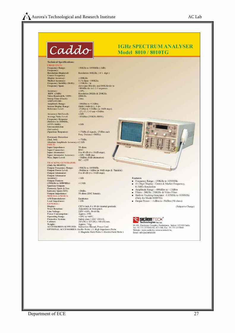
Auroras Technological and Research Institute AC Lab
Department of ECE 27
Auroras Technological and Research Institute AC Lab
Department of ECE 28
EXPERIMENT NO 6
PRE EMPHASIS AND DE EMPHASIS
OBJECTIVE To study the operation of Pre-emphasis and De-emphasis circuits
PRE-LAB
1 Study the theory of Pre-emphasis and De-emphasis circuits
2 Draw the circuit diagram
3 Draw the expected waveforms
COMPONENTS
1 Resistors 100kΩ 100Ω
2 Capacitors 1μf 100μf EQUIPMENT 1 Function generator 1
2 Dual trace CRO 1
THEORY Pre-emphasis
Improving the signal to noise ratio by increasing the magnitude of higher frequency
signals with respect to lower frequency signals
De-emphasis
Improving the signal to noise ratio by decreasing the magnitude of higher
frequency signals with respect to lower frequency signals
Transmitters that employ a true FM modulator require a pre emphasis circuit before the
modulator fore the true FM modulator doesnt automatically pre emphasize the audio like
a transmitter that uses a phase modulator A separate circuit is not necessary for pre
emphasis in a transmitter that has a phase modulator because the phase modulator applies
pre emphasis to the transmitted audio as a function of the phase modulator The receivers
De emphasis circuitry takes the unnatural sounding pre emphasized audio and turns it
back into its original response Pre emphasized (discriminator) audio is however available
directly from the audio demodulation (discriminator) circuitry In linking systems many
choose to eliminate the emphasis circuitry to allow better representation of retransmitted
Auroras Technological and Research Institute AC Lab
Department of ECE 29
signals Since the signal has already been pre emphasized (by the user that is
transmitting) and since the receiver you are listening to takes care of the de emphasis
CIRCUIT DIAGRAMS
PRE-EMPHASIS
DE-EMPHASIS
EXPECTED WAVEFORMS
INPUT
TIME T
A
m
p
l i t u
d
e
Am
Auroras Technological and Research Institute AC Lab
Department of ECE 30
OUTPUT
PRE-EMPHASIS
Freq Vs Gain
DE-EMPHASIS
Freq Vs Gain
TIME T
Freq f (Hz)
A
m
p
l i t u
d
e
Am
Auroras Technological and Research Institute AC Lab
Department of ECE 31
TABLE
PRE EMPHASIS
SNo Input Freq
Input Voltage Vi (Volts)
Output Voltage Vo (Volts) Gain=VoVi
Gain in dB
20log(voVi)
DE-EMPHASIS
SNo Input Freq
Input Voltage Vi (Volts)
Output Voltage Vo (Volts)
Gain=VoVi Gain in dB
20log(VoVi)
PROCEDURE a Pre-emphasis
1 Connect the circuit as per the circuit diagram
2 Apply a constant sine wave input across the input terminal of fixed amplitude(Vi) 3 By varying the input frequency note down the output amplitude (Vo) with respect to
input frequency in Table 4 Calculate the gain using the formula
5 Gain =20log (Vo) (Vi) db
b De-Emphasis
1 Connect the circuit as per the circuit diagram
2 Repeat the steps 2 3 amp4
POST LAB
1 Observe the output amplitude for both the pre-emphasis and De-emphasis circuits
2 Calculate the gain in db
3 Plot the frequency versus gain curves on logarithmic graphs for both the circuits
4 Plot the input and output waveforms Time T VS Voltage Vo
5 Write the result and conclusion
CONCLUSIONS Obtained the pre emphasis and de-emphasis outputs
QUESTIONS 1 Observe the out put signal is disturbed by noise what action has to be taken and measure the
output voltage 2 Where we use the pre emphasis circuit 3 Where we use the de emphasis circuit 4 What are the advantages of pre emphasis and de emphasis circuits
Auroras Technological and Research Institute AC Lab
Department of ECE 32
EXPERIMENT NO 7
TIME DIVISION MULTIPLEXING AND DEMULTIPLEXING
AIM To study Time Division Multiplexing and its waveforms
PRE LAB WORK
Study the operation of Time division multiplexer and demultiplexer Draw the block diagram of TDM
Draw the expected graphs of all necessary waveforms ( CH1CH2TDM OP and Demultiplexed OP)
EQUIPMENT
1) Experimental board on TDM
2) Dual Trace CRO 3) Probes
THEORY
Time Division Multiplexing (TDM) is a technique for transmitting serial messages on a signal
transmission channel by dividing the time division into slots One slot for each message The concept
of TDM comes from sampling theorem which enables use to transmit the information contained in the
band limited Signal using sampling of the signal taken uniformly or a rate slightly higher then the
Nyquist rate TDM enables the joint utilization at a common transmission channel by a number of
independent message sources without mutual interference
The different Ip message signals all band limited in WHz by the IP low pass filters and sequentially
sampled at the transmitters by a rotary switch or a comparator The switch makes are complete
revolution in Ts frac12 W extracting are sample from each IP The commutator OP is a PAM waveform
containing individual message sample
It there are N number of IP the pulse to Pulse spacing will be Ts = 1 while the spacing
N Nfs
bw successive samples from each IP is called a frame
At the receiver a similar rotatory switch the decommutator separates the samples and distributes them
to a bank of low-pass filters which in turn is usually electronic and synchronization signals are
provided to keep the distribute in step with the commutant
Auroras Technological and Research Institute AC Lab
Department of ECE 33
EXPECTED GRAPHS
PROCUDURE
1 Connect the OP of the experimental board to one of the channels on CRO 2 Switch ON the experimental board 3 Observe the OP waveforms 4 Vary the values of the resistors R1 R2 and R3 alternative and observe the OP on CRO
RESULT
The process of the Time Division Multiplexing and the waveforms has been studied
CONCLUSION
Auroras Technological and Research Institute AC Lab
Department of ECE 34
Figure 1 Time Division Multiplexing amp De multiplexing
Auroras Technological and Research Institute AC Lab
Department of ECE 35
EXPERIMENT NO 9
VERIFICATION OF SAMPLING THEOREM
AIM To study the effect of sampling on the transmission of information through PWM
PRE LAB WORK
Study the sampling theorem
Draw the expected graphs of all necessary waveforms ( message signal carrier wave PWM op demodulated op etc
EQUIPMENT
1) Experimental Board on study of sampling theorem 2) Dual trace CRO (0 ndash 20 MHz) 3) Function Generator 4) Connecting wires
THEORY
The principle of sampling can be explained using the switching sampler The switch periodically shifts below bw two constants at the rate of fs = 1 Ts Hz staying on the IP constant for each sampling period The op Xs(t) of the samples consists of segments of x(t) and Xc(t) can be represented as
Xs(t) = X(t) S(t)
Where S(t) is sampling or switching function There are a number of differences bw the ideal sampling and reconstruction techniques described in the proceeding sections of the actual signal
PROCEDURE
1) Observe the internal clock and measure its frequency and amplitude 2) Give the clock to the clock IP terminal 3) Connect the modulating signal to the IP 4) Check the condition fs gt 2fm and observe the de-modulated wave 5) Check the condition fs lt 2fm and fs = 2fm and draw the OP waveforms
RESULT
CONCLUSION
Aurorarsquos Technological and Research Institute DC Lab
36
Figure 2 Sampling Theorem
Aurorarsquos Technological and Research Institute DC Lab
37
EXPERIMENT NO 10
PULSE AMPLITUDE MODULATION AND DEMODULATION
AIM 1) To study the PAM modulation and its waveforms
2) To study the de-modular of PAM
3) To study the effect of sampling frequency on de-modulation OP
PRE LAB WORK
Study the operation Pulse Amplitude Modulator and Demodulator Draw the block diagram of PAM modulator and demodulator Draw the expected graphs of all necessary waveforms ( message signal carrier wave PAM op
demodulated op etc)
EQUIPMENT
1) Exp Board on study of PAM 2) CRO 3) Functional Generator 4) Connecting wires and chords
THEORY
In PAM the amplitude of the carrier wave of higher frequency follow the amp of the message signal
Within this (Modulation Sampling) we have two more types of sampling those are
(1) Natural Sampling
(2) Flat Top Sampling
Basically in Natural Sampling the carrier waves are train of pulses of a certain frequency After
sampling the top of the Pulse follow the message signal Due to this following of top of Pulses with the
message signals cause a distortion in De-modulation
In Flat top sampling also we use train of pulses for sampling but only the starting point of each pulse
follow the message signal remaining width of the pulse will (follow) be flat But here we go for Natural
sampling
EXPECTED WAVEFORMS
Aurorarsquos Technological and Research Institute DC Lab
38
PROCEDURE (MODULATION)
1 Observe the clock on CRO and measure its frequency and amp (freq 5KHz) 2 Connect the clock to clock IP terminals in modulation 3 Put control switch in ac position and set amplitude = OV This provides DC at Modulating
signal terminal 4 Connect the modulating signal or IP to the modulator 5 Connect one channel of CRO at lsquoTirsquo and Gnd Observe that the pulses are of same height
Height is adjustable by varying offset This is PAM signal with DC IP Measure amplitude and frequency of Pulses
6 Increase the amplitude of modulation signal Observe the amplitude and frequency of this sinusoidal modulating signal
7 Observe PAM signal
a) How many Pulses are there in one modulating cycle
b) It is natural or Flat Top PAM c) It is Single or dual polarity PAM
8 Observe the effect of DC offset on PAM waveform
DE-MODULATION
1) Generate undistorted PAM waveform 2) Connect the modulating signal to de-modulation IP 3) Observe the detected OP and measure its frequency which must be same as
modulating signal
EFFECT OF SAMPLING FREQUENCY
1) Connect internal sinusoidal signal to modulating signal IP of the modulator 2) Connect an external functional Generator at the circuit terminals of the modulator 3) Get the PAM waveform using the above circuit 4) Adjust the modulating amplitude offset and frequency to get an undistorted frequency 5) Connect the PAM to de-modulator IP 6) Observe the demodulated signal for various frequencies of clock (fs gt 2fm lt 2fm = 2 fm)
RESULT
CONCLUSION
Aurorarsquos Technological and Research Institute DC Lab
39
Figure 3 Pulse Amplitude Modulation
Auroras Technological and Research Institute AC Lab
Department of ECE 5
EXPERIMENT NO 11
PULSE WIDTH MODULATION AND DEMODULATION
AIM
1) To study the PWM process and the corresponding waveforms 2) To study the effect of sampling frequency on the transmission of information through PWM
PRE LAB WORK
Study the operation Pulse Width Modulator and Demodulator Draw the block diagram of PWM modulator and demodulator Draw the expected graphs of all necessary waveforms ( message signal carrier wave PWM op
demodulated op etc
EQUIPMENT
1) Experimental Board
2) Dual trace CRO 3) AF generator 4) Multimeter
THEORY
In PWM the samples of the message signal are used to vary the duration of the individual pulses The
pulse width may be varied by varying the time of occurrence of the leading edge trailing edge of both
edges of the pulse in accordance with the sampled value of the modulating wave PWM can also be
generated by using emitter follower monostable multivibrator is an excellent voltage to time converter
since its gate width is dependent on the voltage to which the capacitor is changed If this voltage can be
varied in accordance with a signal voltage a series of rectangular pulses can be obtained with width
varying as required
The demodulated of PWM is quite simple PWM is passed through a low pass filter The reconstruction is
associated with a certain amount of Distortion caused by the cross modulator products that fall in the
signal band
EXPECTED WAVEFORM
Aurorarsquos Technological and Research Institute DC Lab
41
PROCEDURE
STUDY OF MODULATION
1) Observe the clock on CRO and measure its frequency (fs) 2) Observe the sine wave modulating signal on CRO and observe the dc shift produced in this
by varying the offset nob Measure the frequency Variation limits of this signal 3) Apply clock at the circuit input terminal 4) Apply modulating signal by keeping the control switch in dc position 5) Observe the modulated wave 6) Plot the graph bw pulse width and the applied dc voltage 7) Put the control switch in sine wave position and adjust the modulating signal amplitude
frequency and dc offset to get the stationary waveform of PWM 8) Note the number of pulses in one circuit of modulating signal
STUDY OF DEMODULATION
1) Generate the stationary PWM waveform using sin wave modulating signal 2) Connect the modulator OP to PWM demodulator 3) Connect Channel (1) to Modulating Signal and channel (2) to demodulated wave
EFFECT OF SAMPLING FREQUENCY
1) Use an external square wave and connect it to the clock input 2) Set the frequency of square wave at frequency 2fm 3) Observe the demodulated wave
4) Change the frequency of square wave to fs lt 2fm fs gt 2fm and observe the demodulated wave
RESULT
CONCLUSION
Aurorarsquos Technological and Research Institute DC Lab
42
Figure 4 Pulse Width Modulation
Aurorarsquos Technological and Research Institute DC Lab
43
EXPERIMENT NO 12
PULSE POSITION MODULATION AND DEMODULATION
AIM
1) To study the PPM Modulation and the corresponding waveforms 2) To study the de-modulation of PPM 3) To see the effect of sampling frequency on the transmission of information through PPM
PRE LAB WORK
Study the operation Pulse Position Modulator and Demodulator Draw the block diagram of PPM modulator and demodulator Draw the expected graphs of all necessary waveforms ( message signal carrier wave PPM op
demodulated op etc
EQUIPMENT
1) Experimental Board for PPM
2) Dual Phase Oscilloscope
3) AF Generator
THEORY
In PDM long pulses expand considerable power duration If the pulse which bearing no additional
information If this un used power is subtracted from PDM so that only time transitions are preserved
We observe a more efficient type of pulse modulation known as pulse position modulation Here in the
Pulse Position Modulated wave the position of the Pulse relative to its unmodulated time of occurrence is
varied in accordance with the message signal
We generate a PPM wave from PWM wave by using a Monostable Multivibrator The device has one
absolutely stable state and one quest ndash stable state into which it is triggered by an externally applied Pulse
The monostable multivibrator is designed to trigger on the trailing edges of the duration ndash modulated pulse
is varied in accordance with the message signal
The fixed pulse duration of the PPM wave at the monostable multivibrator OP can be set by appropriately
choosing the resistance ndash capacitance combination in the timing circuit of the device
Aurorarsquos Technological and Research Institute DC Lab
44
EXPECTED WAVEFORM
PROCEDURE
STUDY OF MODULATION
Observe the clock and measure its frequency (fs) Apply the clock at the clock IP terminal in the modulator Apply the modulating signal keeping control switch in DC position Observe the PPM OP Connect the channel ndash (1) on CRO to clock and channel (2) to PPM wave OP Compare the position of two waveforms Vary the DC offset and observe the relative shift between the clock and PPM OP Measure the time shift between clock and PPM wave for various settings of offset Draw the graph between time shift and DC voltage Put the control switch in AC position adjusts the amplitude and frequency and offset
of sinusoidal modulating signal to get the stationary PPM wave Note the number of pulses in one cycle of the modulated wave
STUDY OF DEMODULATION
Generate a stationery PPM wave for a sinusoidal modulating signal Apply the PPM wave to the input of de-modulator Connect the Channel ndash (1) of CRO to the modulating signal and channel ndash 2 to the
de-modulator output Compare the two waveforms
Note the frequency of demodulated wave It should be same as the modulating signal Note down the waveform
RESULT
CONCLUSION
Aurorarsquos Technological and Research Institute DC Lab
45
Aurorarsquos Technological and Research Institute DC Lab
46
Figure 5 Pulse Position Modulation
Aurorarsquos Technological and Research Institute AC Lab
47
EXPERIMENT NO 13
FREQUENCY SYNTHESIZER
AIM
To study the operation of frequency synthesizer using PLL
PRE-LAB 1 Study the data sheet of IC 7404IC 4017IC 565 and IC 4046
2 Study the theory of frequency synthesizer 3 Draw the circuit diagram and expected waveforms
EQUIPMENTS
1 Frequency synthesizer trainer AET -26A
2 Dual trace CRO (20Mhz) 3 Digital frequency counter or multimeter
4 Patch chords
THEORY
A frequency synthesizer is an electronic system for generating any of a range
of frequencies from a single fixed time base or oscillator They are found in many modern
devices including radio receivers mobile telephones radiotelephones walkie-talkies CB
radios satellite receivers GPS systems etc A frequency synthesizer can combine
frequency multiplication frequency division and frequency mixing (the frequency mixing
process generates sum and difference frequencies) operations to produce the desired output
signal
BLOCK DIAGRAM
Phase Comparator
Amplifier Low pass filter
V C O
Div N Network frequency divider
Fin= fout
N
fin
Fout =Nf in
Aurorarsquos Technological and Research Institute AC Lab
48
SIMPLE 1KHZ-9KHZ FREQUENCY SYNTHESIZER
CIRCUIT DAIGRAM
PROCEDURE 1 Switch on the trainer ad verify the output of the regulated power supply ie 5V These
supplied are internally connected to the circuit so no extra connections are required 2 Observe output of the square wave generator using oscilloscope and measure the range
with the help of frequency counter frequency range should be around 1KHz to 10KHz 3 Calculate the free running frequency range of the circuit (VCO output between 4th pin
and ground 1 For different values of timing resistor R1 ( to measure Rt value using digital multimeter between given test points 1 And record the frequency values in table 1
Fout = 03 (RtCt) where Rt is the timing resistor and Ct is the timing capacitor = 001 f
Aurorarsquos Technological and Research Institute AC Lab
49
4 Connect 4th pin of LM 565 (Fout) to the driver stage and 5th pin (Phase comparator) connected to 11th pin of 7404 Output can be taken at the 11th pin of the 7490 It should be divided by the 2 amp 3 times of the fout
TABULATION
Fin KHz Fout = N x fin KHz Divided by 3 2
EXPECTED WAVEFORMS
POST LAB
1 Observe the synthesized output in table 2 Calculate the output frequency
3 Plot the output waveforms
4 Write result and conclusions
CONCLUSIONS
The various outputs of frequency synthesizer are verified
QUESTIONS
1 What are the applications of frequency synthesizer
TIME T
A
m
p
l i T
u
d
e
Ac
Aurorarsquos Technological and Research Institute AC Lab
50
2 What is the difference between heterodyning and synthesizer
Aurorarsquos Technological and Research Institute AC Lab
51
EXPERIMENT NO 14
AGC CHARATERISTICS
AIM
To observe the effect of automatic gain control(AGC)
PRE LAB 1 To study the theory of AGC 2 Draw the Block Diagram circuits diagram and expected waveforms
EQUIPMENTS 1 AGC Trainer Kit 2 CRO
3 Patch Chords
4 Digital Multimeter
THEORY
Automatic gain control (AGC) is an adaptive system found in many electronic
devices The average output signal level is fed back to adjust the gain to an appropriate level
for a range of input signal levels For example without AGC the sound emitted from an AM
radio receiver would vary to an extreme extent from a weak to a strong signal the AGC
effectively reduces the volume if the signal is strong and raises it when it is weaker AGC
algorithms often use a PID controller where the P term is driven by the error between
expected and actual output amplitude
Block Diagram
Frequency Converter
1st IF Amplifier
2nd IF Amplifier
Detector
Audio Preamplifier
Driver Output
Aurorarsquos Technological and Research Institute AC Lab
52
CIRCUIT DIAGRAM
PROCEDURE
1 Connect 455 KHz IF Signal Function Generator connect AGC link Connect CRO channel-1 at input terminals
2 Connect CRO channel 2 at collector of Q3 The amplified signal will be observed 3 Calculate the voltage gain by measuring the amplitude of output signal (Vo) waveform
using formula A=VoVi 4 Now connect CRO-2 channel at output The detected audio signal of 455 Khz will be
observed 5 Now vary input level of 455 KHz IF signal and observe detected 455 KHz audio signal
with and without AGC link The output will be distorted when AGC link is removed ie there is no AGC action
6 This explains AGC effect in Radio circuit
TABULATION
SNo Input Voltage Vi (P-P) With out AGC With AGC
Output Voltage Vo (P-P)
Gain A= Vo Vi
Output Voltage Vrsquoo (P-P)
Gain Arsquo= Vrsquoo Vi
Aurorarsquos Technological and Research Institute AC Lab
53
EXPECTED WAVEFORMS
AM Modulated RF Input
Detected Output with AGC
Detected Output without AGC
POST-LAB
1 Observe the input voltage and output voltage for with AGC and Without AGC in Table 1
2 Calculate Gain a=vovi for both cases 3 Plot the output waveforms Time T Vs Voltage Vo and input voltage Vi Vs Gain A 4 Write Result and Conclusions
CONCLUSIONS The AGC characteristics are verified
QUESTIONS 1 what is meant by AGC
2 What is the difference between simple AGC and delayed AGC
3 From which part of receiver AGC is obtained
TIME T
A
m
p
l i T
u
d
e
Ac
TIME T
A
m
p
l i T
u
d
e
Ac
TIME T
A
m
p
l i T
u
d
e
Ac
Aurorarsquos Technological and Research Institute AC Lab
54
EXPERIMENT NO 15
PHASE LOCKED LOOP
OBJECTIVE To study the Phase locked loop using 565 IC and to take input frequency given by an external signal source
PRE-LAB To Study
1 The data sheet of IC 565
2 The theory of Phase locked loop
3 About free running frequency locking range and capture range
4 Draw the circuit diagram and expected waveforms
EQUIPMENT 1 Function generator 2
2 Dual trace CRO 1
3 Phase locked loop trainer kit
THEORY
A phase-locked loop or phase lock loop (PLL) is a control system that generates a signal
that has a fixed relation to the phase of a reference signal A phase-locked loop circuit
responds to both the frequency and the phase of the input signals automatically raising or
lowering the frequency of a controlled oscillator until it is matched to the reference in both
frequency and phase A phase-locked loop is an example of a control system using negative
feedback Phase-locked loops are widely used in radio telecommunications computers and
other electronic applications They may generate stable frequencies recover a signal from a
noisy communication channel or distribute clock timing pulses in digital logic designs
such as microprocessors Since a single integrated circuit can provide a complete phase-
locked-loop building block the technique is widely used in modern electronic devices
with output frequencies from a fraction of a cycle per second up to many gigahertz
BLOCK DIAGRAM
Aurorarsquos Technological and Research Institute AC Lab
55
CIRCUIT DIAGRAM
PROCEDURE 1 Switch ON the trainer kit 2 Check the VCO output at pin 4 of IC 565 that is a square wave form The frequency of the
VCO Output depends on CT (001f) and RT (47kΩ) 3 Next short the pins 4amp5 and give signal of variable frequency and observe VCO output 4 Change the input frequency and observe the VCO output on the CRO 5 Between some frequencies the VCO output is locked to the input signal frequency This can
be observed by increasing or decreasing the frequency of the VCO output by changing input frequency
6 Before or after that frequency range the VCO output is not locked
7 Calculate Lock range (FL) and capture range (FC) by using the following formulas
FL = 8foVCO fo=03RtCT
FC=12π radic2πf236103 C2
Table1
SNo Locking Frequency Frequency Range From To
CHARTERISTICES
Aurorarsquos Technological and Research Institute AC Lab
56
CONCLUSIONS Obtained the lock range of PLL
QUESTIONS
1 Observe the VCO output when pins 4amp5 short and give square wave as signal 2 Define lock range and capture range
3 What are the basic applications of PLL
Aurorarsquos Technological and Research Institute AC Lab
57
ANNEXURE-I
EXPERIMENT NO 1
Aurorarsquos Technological and Research Institute AC Lab
58
CHARACTERISTICS OF MIXER
AIM
To study the functioning of a frequency mixer
PRE LAB 1 To study the theory of Mixer 2 Draw the circuit diagram and expected waveforms
EQUIPMENTS 1 Frequency mixer trainer kit 2 CRO (20MHz) 3 Connecting cords and probes 4 Function generator (1MHz)
THEORY
In receivers using the super heterodyne principle a signal at variable frequency is
converted to a fixed lower frequency IF before detection IF is called the intermediate frequency
In typical AM (Amplitude Modulation eg as used on medium wave) home receivers that
frequency is usually 455 kHz for FM VHF receivers it is usually 107 MHz An intermediate
frequency (IF) is a frequency to which a carrier frequency is shifted as an intermediate step in
transmission or reception Frequency modulation (FM) is a form of modulation that represents
information as variations in the instantaneous frequency of a carrier wave Very high frequency
(VHF) is the radio frequency range from 30 MHz (wavelength 10 m) to 300 MHz (wavelength 1
heterodyne receivers mix all of the incoming signals with an internally generated waveform
called the local oscillator The user tunes the radio by adjusting the sets oscillator frequency in
the mixer stage of a receiver the local oscillator signal multiplies with the incoming signals
which shifts them all down in frequency The one that shifts is passed on by tuned circuits
amplified and then demodulated to recover the original audio signal The oscillator also shifts a
copy of each incoming signal up in frequency by amount Those very high frequency images
are all rejected by the tuned circuits in the IF stage The Super heterodyne receiver (or to give it its
full name The Supersonic Heterodyne Receiver usually these days shortened to superhet) was
invented by Edwin Armstrong in 1918
Aurorarsquos Technological and Research Institute AC Lab
59
BLOCK DIAGRAM
CIRCUIT DIAGRAM
EXPECTED WAVEFORMS
INPUT SIGNAL Fx
INPUT SIGNAL Fy
TIME T
A
m
p
l i T
u
d
e
Ac
Aurorarsquos Technological and Research Institute AC Lab
60
MIXER OUTPUT(Fy-Fx)
PROCEDURE 1 Connect the circuit as per the given circuit diagram 2 Switch on the power supply of trainer kit 3 Apply a sine wave at input Fx of 2 VP-P amplitude and 100 KHz frequency 4 Apply a sine wave at input FY of 2 VP-P amplitude and 100 KHz frequency 5 Observe the output waveform on the CRO 6 Repeat the steps 34 and 5 by changing the values of Fx once greater than and less than
FY in a steps of 5Khz (in the range 80KHz to 120KHz)
TABULATION
TIME T
A
M
P
L
I T
U
D
E
TIME T
A
m
p
l i T
u
d
e
Ac
Aurorarsquos Technological and Research Institute AC Lab
61
SNo Freq (Fy)
(kHz) Amp(V) Freq(Fx) (kHz) Amp(V) Freq(Fy-Fx)
(kHz) Amp(V)
POST LAB 1 Observe the amplitude and time Of inputs and output in table
2 Draw the expected waveforms
3 Verify the output signal obtained with the theoretical value 4 Plot the graphs for Time T VS input signal (FX) Voltage V input signal (FY) Voltage V
and output Signal F(x-y) voltage V 5 Write result and conclusions
CONCLUSIONS
Obtained the output of the mixer for various inputs
QUESTIONS
1 what are the different types of mixtures available
2 What is meant by heterodyning
3 What is meant by IF
Aurorarsquos Technological and Research Institute AC Lab
62
EXPERIMENT NO 2
DIGITAL PHASE DETECTOR
OBJECTIVE To detect the phase difference between two square wave signals using digital phase detector
PRE LAB
1 To study the theory of digital phase detector and EX-OR gate operation and truth table 2 Draw the circuit diagram and expected output and input waveforms
EQUIPMENT 1 Digital phase detector trainer kit 2 Regulated power supplies
3 CRO (20MHz) 4 Connecting cords amp probes
5 Digital frequency counter or multimeter
THEORY
Phase detector is a frequency mixer or analog multiplier circuit that generates a voltage
signal which represents the difference in phase between two signal inputs It is an essential
element of the phase-locked loop (PLL)Detecting phase differences is very important in many
applications such as motor control radar and telecommunication systems servo mechanisms and
demodulators
Electronic phase detector
Some signal processing techniques such as those used in radar may require both the amplitude
and the phase of a signal to recover all the information encoded in that signal One technique is to
feed an amplitude-limited signal into one port of a product detector and a reference signal into the
other port the output of the detector will represent the phase difference between the signals If the
signal is different in frequency from the reference the detector output will be periodic at the
difference frequency Phase detectors for phase-locked loop circuits may be classified in two
types A Type I detector is designed to be driven by analog signals or square-wave digital signals
and produces an output pulse at the difference frequency The Type I detector always produces an
output waveform which must be filtered to control the phase-locked loop variable frequency
oscillator (VCO) A type II detector is sensitive only to the relative timing of the edges of the input
and reference pulses and produces a constant output proportional to phase difference when both
signals are at the same frequency This output will tend not to produce ripple in the control voltage
of the VCO
Aurorarsquos Technological and Research Institute AC Lab
63
BLOCK DIAGRAM OF PLL
CIRCUIT DIAGRAM
Aurorarsquos Technological and Research Institute AC Lab
64
EXPECTED WAVEFORMS
EX-OR PHASE DETECTOR
EDGE TRIGGERED OUTPUT
PROCEDURE
1 Switch on the trainer kit
2 Observe the output of the square wave generator available on the trainer kit using CRO
and measure the range with the help of frequency counter the frequency range should be
around 2 KHz to 13 KHz
3 Calculate the free running range of the VCO output ie between 4th pin of IC PLL 565
and ground For different values of timing resistor Rt fout is given by Fout =03 Rt Ct
where Ct timing capacitor = 001 μF Rt timing resistor
4 Connect the square wave to the input of IC PLL 565 and short 4th and 5th pin of PLL
Vary the input frequency of the square wave when the PLL is locked that is connected to
Aurorarsquos Technological and Research Institute AC Lab
65
one input fout EX-OR phase detector The other input fin of EX-OR phase detector is the
coming from inbuilt of square wave generator
5 Connect the pulse generator output to the input of IC 565 PLL and short 4th amp 5th pin of
PLL Vary the input frequency of the square wave when the PLL is locked that is
connected to one input of Edge triggered phase detector input ie fout The other input fin
of edge triggered phase detector is the pulse input coming from the inbuilt pulse generator
6 The dc output voltage of the exclusive-OR phase detector is a function of the phase
difference between its two inputs fin and fout
POST LAB
1 Observe the Voltage and Time of the two input square waves
2 Observe difference of two inputs as square wave output
3 Plot the inputs and output waveforms Time T VS Voltage V
CONCLUSIONS
The phase detector outputs are verified
QUESTIONS
1 What is the function of phase detector
2 What is the condition for getting maximum output
3 Advantages of digital phase detector over analog phase detector
Aurorarsquos Technological and Research Institute AC Lab
66
EXPERIMENT NO 3
COASTAS RECEIVER
AIM
To demodulate a DSB-SC signal using coastas receiver
PRE LAB 1 To study the operation of coastas receiver 2 Draw the circuit diagram and expected waveforms
EQUIPMENTS 1 Communications trainer kit 2 DSB-SC modulator trainer kit 3 CRO (20MHz) 4 Connecting cords and probes 5 Function generator (1MHz)
THEORY
This loop and its variations is much-used as a method of carrier acquisition (and
simultaneous message demodulation) in communication systems both analog and digital
It has the property of being able to derive a carrier from the received signal even when there is
no component at carrier frequency present in that signal (eg DSBSC) The requirement is that
the amplitude spectrum of the received signal be symmetrical about this frequency
The Costas loop is based on a pair of quadrature modulators - two multipliers
fed with carriers in phase-quadrature These multipliers are in the in-phase (I) and quadrature
phase (Q) arms of the arrangement Each of these multipliers is part of separate synchronous
demodulators The outputs of the modulators after filtering are multiplied together in a third
multiplier and the lowpass components in this product are used to adjust the phase of the local
carrier source - a VCO - with respect to the received signal The operation is such as to
maximise the output of the I arm and minimize that from the Q arm The output of the I arm
happens to be the message and so the Costas loop not only acquires the carrier but is a
(synchronous) demodulator as well A complete analysis of this loop is non-trivial It would
include the determination of conditions for stability and parameters such as lock range capture
range and so on
Aurorarsquos Technological and Research Institute AC Lab
67
BLOCK DIAGRAM
EXPECTED WAVEFORMS
DSB-SC modulated output
Aurorarsquos Technological and Research Institute AC Lab
68
Demodulated output of the coastas loop
PROCEDURE
1 Switch ON the DSB-SC trainer kit
2 Generate the carrier and modulating signal
3 Generate the DSB-SC modulated signal
4 Connect the required blocks of the coastas receiver in the communications kit
5 Apply the generated DSB-SC signal to the above connected coastas receiver
6 Observe that the output of the coastas receiver is the demodulated wave of DSB-SC signal
POST LAB
1 Observe the frequency and amplitude of the carrier and modulating signal
2 Observe the frequency and amplitude of the balanced modulator output
3 Observe the lock condition of the coastas loop
4 observe the output of the coastas demodulator
5 Write result and conclusions
CONCLUSIONS The balanced modulator output and the operation of coastas receiver is verified
QUESTIONS 1 what is the operation of coastas loop
2 What happens when the locking condition of the coastas loop occurs
3 Coastas loop can be used for demodulation of other modulation techniques also What are they
Aurorarsquos Technological and Research Institute AC Lab
69
MATLAB PROGRAMMES
Aurorarsquos Technological and Research Institute AC Lab
70
INDEX
1 Introduction - 70
2 Amplitude Modulation and Demodulation - 74
3 DSB-SC Modulation and Demodulation - 84
4 SSB-SC Modulation and Demodulation - 89
5 Frequency Modulation and Demodulation - 95
6 Phase Modulation and Demodulation - 99
7 Time Division Multiplexing and Demultiplexing - 100
8 Frequency Division Multiplexing and Demultiplexing- 103
9 Verification of Sampling Theorem - 104
10 Pulse Amplitude Modulation and Demodulation - 106
11 Pulse width Modulation and Demodulation - 108
12 Pulse Position Modulation and Demodulation - 110
13 PLL as FM Demodulator - 112
Aurorarsquos Technological and Research Institute AC Lab
71
1 INTRODUCTION
What Is Simulink
Simulink is a software package for modeling simulating and analyzing dynamic
systems It supports linear and nonlinear systems modeled in continuous time sampled time
or a hybrid of the two Systems can also be multirate ie have different parts that are
sampled or updated at different rates
Tool for Simulation
Simulink encourages you to try things out You can easily build models from scratch
or take an existing model and add to it You have instant access to all the analysis tools in
MATLABreg so you can take the results and analyze and visualize them A goal of Simulink
is to give you a sense of the fun of modeling and simulation through an environment that
encourages you to pose a question model it and see what happens
Simulink is also practical With thousands of engineers around the world using it to
model and solve real problems knowledge of this tool will serve you well throughout your
professional career
Tool for Model-Based Design
With Simulink you can move beyond idealized linear models to explore more realistic
nonlinear models factoring in friction air resistance gear slippage hard stops and the other
things that describe real-world phenomena Simulink turns your computer into a lab for
modeling and analyzing systems that simply wouldnt be possible or practical otherwise
whether the behavior of an automotive clutch system the flutter of an airplane wing the
dynamics of a predator-prey model or the effect of the monetary supply on the economy
For modeling Simulink provides a graphical user interface (GUI) for building models
as block diagrams using click-and-drag mouse operations With this interface you can draw
the models just as you would with pencil and paper (or as most textbooks depict them) This
is a far cry from previous simulation packages that require you to formulate differential
equations and difference equations in a language or program Simulink includes a
comprehensive block library of sinks sources linear and nonlinear components and
connectors You can also customize and create your own blocks For information on creating
your own blocks see the separate Writing S-Functions guide
Models are hierarchical so you can build models using both top-down and bottom-up
approaches You can view the system at a high level then double-click blocks to go down
through the levels to see increasing levels of model detail This approach provides insight into
how a model is organized and how its parts interact
After you define a model you can simulate it using a choice of integration methods either
from the Simulink menus or by entering commands in the MATLAB Command Window The
menus are particularly convenient for interactive work while the command-line approach is
very useful for running a batch of simulations (for example if you are doing Monte Carlo
simulations or want to sweep a parameter across a range of values) Using scopes and other
display blocks you can see the simulation results while the simulation is running In addition
Aurorarsquos Technological and Research Institute AC Lab
72
you can change many parameters and see what happens for what if exploration The
simulation results can be put in the MATLAB workspace for post processing and
visualization
Model analysis tools include linearization and trimming tools which can be accessed
from the MATLAB command line plus the many tools in MATLAB and its application
toolboxes And because MATLAB and Simulink are integrated you can simulate analyze
and revise your models in either environment at any point
1 Generation of cosine wave in time domain and frequency
domain Clc clear all close all x = -500015 t = 0140001 time = cos(23141000t) y1 = cos(23141000x) subplot(211) plot(xy1) axis([-5 5 -3 3]) grid on title(Time domain) xlabel(Time ) ylabel(Amplitude) now create a frequency vector for the x-axis and plot the magnitude and phase subplot(212) fre = abs(fft(time)) f = (0length(fre) - 1)4000length(fre) plot(ffre) grid on title(Frequency domain (Spectrum)) xlabel(Freq ) ylabel(Amplitude)
WAVEFORMS
Aurorarsquos Technological and Research Institute AC Lab
73
2 Generation of square wave in time domain and frequency
domain
clc clear all close all x = -500015 Fs = 399 t = 01Fs1 time = SQUARE(2pi1000t) y1 = SQUARE(23141000x) subplot(211) plot(xy1) axis([-5 5 -3 3]) grid on xlabel(Time domain) ylabel(Amplitude) now create a frequency vector for the x-axis and plot the magnitude and phase subplot(212) fre = abs(fft(time)) f = (0length(fre) - 1)Fslength(fre) plot(ffre) grid on xlabel(Freq domain) ylabel(Amplitude)
WAVEFORMS
Aurorarsquos Technological and Research Institute AC Lab
74
Aurorarsquos Technological and Research Institute AC Lab
75
2 AMPLITUDE MODULATION AND DEMODULATION PROGRAM 1
clc clear all close all Ac=1 Carrier Amplitude Fc=04 Carrier frequency Fm=005 baseband frequency Fs=10 sampling t=001200 mt=cos(2piFmt) under modulation mu=05 st=Ac(1+mumt)cos(2piFct) subplot(211) plot(tst) hold on plot(tAc(mumt+ones(1length(mt)))r) plot(t-Ac(mumt+ones(1length(mt)))r) hold off title(Modulation Index = 05 under modulation Ac(1+05cos(2pi005t))cos(2pi04t)) xlabel(time (s))ylabel(amplitude) st_fft=fft(st) st_fft=fftshift(st_fft) st_fft_fre=5linspace(-11length(st_fft)) subplot(212) plot(st_fft_freabs(st_fft)) title(spectrum with Modulation Index = 05) xlabel(Frequency (Hz))axis([-1 1 0 1000Ac+100])
total modulation figure mu=1 st=Ac(1+mumt)cos(2piFct) subplot(211) plot(tst) hold on plot(tAc(mumt+ones(1length(mt)))r) plot(t-Ac(mumt+ones(1length(mt)))r) hold off title(Modulation Index = 1 modulation Ac(1+1cos(2pi005t))cos(2pi04t)) xlabel(time (s))ylabel(amplitude) st_fft=fft(st) st_fft=fftshift(st_fft) st_fft_fre=Fs2linspace(-11length(st_fft)) subplot(212) plot(st_fft_freabs(st_fft)) title(spectrum with Modulation Index = 1) xlabel(Frequency (Hz))axis([-1 1 0 1000Ac+100])
Aurorarsquos Technological and Research Institute AC Lab
76
over Modulation figure mu=2 st=Ac(1+mumt)cos(2piFct) subplot(211) plot(tst) hold on plot(tAc(mumt+ones(1length(mt)))r) plot(t-Ac(mumt+ones(1length(mt)))r) hold offtitle(Modulation Index = 2 over modulation Ac(1+2cos(2pi005t))cos(2pi04t)) xlabel(time (s))ylabel(amplitude) st_fft=fft(st) st_fft=fftshift(st_fft) st_fft_fre=Fs2linspace(-11length(st_fft)) subplot(212) plot(st_fft_freabs(st_fft)) title(spectrum with Modulation Index = 2) xlabel(Frequency (Hz))axis([-1 1 0 1000Ac+100])
WAVEFORMS
Aurorarsquos Technological and Research Institute AC Lab
77
PROGRAM 2
Aurorarsquos Technological and Research Institute AC Lab
78
task 1 fc=154000
task 2 fm=fc10 fs=100fc t=01fs4fm xc=cos(2pifct) xm=cos(2pifmt) figure(1) subplot(211)plot(txc) title(carrier signal of 154 khz) xlabel(time (sec)) ylabel(amplitude) subplot(212)plot(txm) title(message signal of 154 khz) xlabel(time (sec)) ylabel(amplitude) DSB-SC MODULATION mu = input( enter the Modulation Index value ) z1=(1+muxm)xc figure(2)
task 31 subplot(211)plot(tz1) title(AMPLITUDE MODULATION IN TIME DAOMAIN) xlabel(time (sec)) ylabel(amplitude)
task 32 l1=length(z1) f=linspace(-fs2fs2l1) Z1=fftshift(fft(z1l1)l1) subplot(212)plot(fabs(Z1)) title(AMPLITUDE MODULATION IN FREQUENCY DOMAIN) xlabel(frequency(hz)) ylabel(amplitude) axis([-200000 200000 0 03])
task 33 demodulation s1=z1xc S1=fftshift(fft(s1length(s1))length(s1)) figure(3) plot(fabs(S1)) title( demodulated signal IN FREQUENCY DOMAIN before filtring) xlabel(frequency(hz)) ylabel(amplitude) axis([-200000 200000 0 03]) hold on Hlp=1sqrt(1+(ffc)^(2100)) plot(fHlpr) title( frequency response of low pass filter) xlabel(frequency(hz)) ylabel(amplitude) axis([-200000 200000 0 2])
task 34 E1=HlpS1 figure(4) subplot(211)plot(fE1)
Aurorarsquos Technological and Research Institute AC Lab
79
title( Recover signal IN FREQUENCY DOMAIN after filtring) xlabel(frequency(hz)) ylabel(amplitude) axis([-200000 200000 0 03]) e1=ifft(ifftshift(E1))length(E1) subplot(212)plot(t(105)e1) title( Recover signal IN Time DOMAIN after filtring) xlabel(time(sec)) ylabel(amplitude)
WAVEFORMS
enter the Modulation Index value 05
0 1 2 3
x 10-4
-1
-05
0
05
1carrier signal of 154 khz
time (sec)
am
plit
ude
0 1 2 3
x 10-4
-1
-05
0
05
1message signal of 154 khz
time (sec)
am
plit
ude
Aurorarsquos Technological and Research Institute AC Lab
80
0 1 2 3
x 10-4
-2
-1
0
1
2AMPLITUDE MODULATION IN TIME DAOMAIN
time (sec)
am
plit
ude
-2 -15 -1 -05 0 05 1 15 2
x 105
0
01
02
AMPLITUDE MODULATION IN FREQUENCY DOMAIN
frequency(hz)
am
plit
ude
-2 -15 -1 -05 0 05 1 15 2
x 105
0
02
04
06
08
1
12
14
16
18
2 frequency response of low pass filter
frequency(hz)
am
plit
ude
Aurorarsquos Technological and Research Institute AC Lab
81
enter the Modulation Index value 1
-2 -15 -1 -05 0 05 1 15 2
x 105
0
01
02
Recover signal IN FREQUENCY DOMAIN after filtring
frequency(hz)
am
plit
ude
0 1 2 3
x 10-4
05
1
15
2 Recover signal IN Time DOMAIN after filtring
time(sec)
am
plit
ude
0 1 2 3
x 10-4
-2
-1
0
1
2AMPLITUDE MODULATION IN TIME DAOMAIN
time (sec)
am
plit
ude
-2 -15 -1 -05 0 05 1 15 2
x 105
0
01
02
AMPLITUDE MODULATION IN FREQUENCY DOMAIN
frequency(hz)
am
plit
ude
Aurorarsquos Technological and Research Institute AC Lab
82
enter the Modulation Index value 2
-2 -15 -1 -05 0 05 1 15 2
x 105
0
02
04
06
08
1
12
14
16
18
2 frequency response of low pass filter
frequency(hz)
am
plit
ude
-2 -15 -1 -05 0 05 1 15 2
x 105
0
01
02
Recover signal IN FREQUENCY DOMAIN after filtring
frequency(hz)
am
plit
ude
0 1 2 3
x 10-4
0
1
2
3 Recover signal IN Time DOMAIN after filtring
time(sec)
am
plit
ude
Aurorarsquos Technological and Research Institute AC Lab
83
0 1 2 3
x 10-4
-4
-2
0
2
4AMPLITUDE MODULATION IN TIME DAOMAIN
time (sec)
am
plit
ude
-2 -15 -1 -05 0 05 1 15 2
x 105
0
01
02
AMPLITUDE MODULATION IN FREQUENCY DOMAIN
frequency(hz)
am
plit
ude
-2 -15 -1 -05 0 05 1 15 2
x 105
0
02
04
06
08
1
12
14
16
18
2 frequency response of low pass filter
frequency(hz)
am
plit
ude
Aurorarsquos Technological and Research Institute AC Lab
84
-2 -15 -1 -05 0 05 1 15 2
x 105
0
01
02
Recover signal IN FREQUENCY DOMAIN after filtring
frequency(hz)
am
plit
ude
0 1 2 3
x 10-4
-2
0
2
4 Recover signal IN Time DOMAIN after filtring
time(sec)
am
plit
ude
Aurorarsquos Technological and Research Institute AC Lab
85
3 DOUBLE SIDEBAND ndash SUPRESSED CARRIER MODULATION
AND DEMODULATION
PROGRAM 1 clc clear all close all Ts = 199 subplot(411) t = 01Ts1 m = cos(2pi1000t) plot(tm) title(Modulating Signal ) xlabel(Time) ylabel(Amplitude) grid on plot of the carrier signal
subplot(412) c = cos(2pi5000t) plot(tc) title(Carrier Signal ) xlabel(Time) ylabel(Amplitude) grid on plot of the DSB signal with Suppresed carrier intime domain
subplot(413) d = mc plot(td) title(DOUBLE SIDEBAND ndash SUPRESSED CARRIER SIGNAL ) xlabel(Time) ylabel(Amplitude) grid on freq domain of the DSB signal
subplot(414) fre = abs(fft(d)) f = (0length(fre) - 1)Tslength(fre) plot(ffre) axis([0 100 0 50]) grid on title(DOUBLE SIDEBAND ndash SUPRESSED CARRIER SPECTRUM ) xlabel(Freq domain) ylabel(Amplitude)
Aurorarsquos Technological and Research Institute AC Lab
86
WAVEFORMS
0 01 02 03 04 05 06 07 08 09 1-1
0
1Modulating Signal
Time
Am
plit
ude
0 01 02 03 04 05 06 07 08 09 1-1
0
1Carrier Signal
Time
Am
plit
ude
0 01 02 03 04 05 06 07 08 09 1-1
0
1DOUBLE SIDEBAND ndash SUPRESSED CARRIER SIGNAL
Time
Am
plit
ude
0 10 20 30 40 50 60 70 80 90 1000
50DOUBLE SIDEBAND ndash SUPRESSED CARRIER SPECTRUM
Freq domain
Am
plit
ude
Aurorarsquos Technological and Research Institute AC Lab
87
PROGRAM 2 task 1 fc=154000 task 2 fm=fc10 fs=100fc t=01fs4fm xc=cos(2pifct) xm=cos(2pifmt) figure(1) subplot(211)plot(txc) title(carrier signal of 154 khz) xlabel(time (sec)) ylabel(amplitude) subplot(212)plot(txm) title(message signal of 154 khz) xlabel(time (sec)) ylabel(amplitude) DSB-SC MODULATION z1= xmxc figure(2) task 31 subplot(211)plot(tz1) title(DSB-SC MODULATION IN TIME DAOMAIN) xlabel(time (sec)) ylabel(amplitude) task 32 l1=length(z1) f=linspace(-fs2fs2l1) Z1=fftshift(fft(z1l1)l1) subplot(212)plot(fabs(Z1)) title(DSB SC MODULATION IN FREQUENCY DOMAIN) xlabel(frequency(hz)) ylabel(amplitude) axis([-200000 200000 0 03]) task 33 demodulation s1=z1xc S1=fftshift(fft(s1length(s1))length(s1)) figure(3) plot(fabs(S1)) title( demodulated signal IN FREQUENCY DOMAIN before filtring) xlabel(frequency(hz)) ylabel(amplitude) axis([-200000 200000 0 03]) hold on Hlp=1sqrt(1+(ffc)^(2100)) plot(fHlpg) title( frequency response of low pass filter) xlabel(frequency(hz)) ylabel(amplitude) axis([-200000 200000 0 2]) task 34 E1=HlpS1 figure(4) subplot(211)plot(fE1) title( Recover signal IN FREQUENCY DOMAIN after filtring) xlabel(frequency(hz)) ylabel(amplitude) axis([-200000 200000 0 03]) e1=ifft(ifftshift(E1))length(E1) subplot(212)plot(t(105)e1)
Aurorarsquos Technological and Research Institute AC Lab
88
title( Recover signal IN Time DOMAIN after filtring) xlabel(time(sec)) ylabel(amplitude) WAVEFORMS
0 1 2 3
x 10-4
-1
-05
0
05
1carrier signal of 154 khz
time (sec)
ampl
itude
0 1 2 3
x 10-4
-1
-05
0
05
1message signal of 154 khz
time (sec)
ampl
itude
0 1 2 3
x 10-4
-1
-05
0
05
1DSB-SC MODULATION IN TIME DAOMAIN
time (sec)
ampl
itude
-2 -15 -1 -05 0 05 1 15 2
x 105
0
01
02
DSB SC MODULATION IN FREQUENCY DOMAIN
frequency(hz)
ampl
itude
Aurorarsquos Technological and Research Institute AC Lab
89
-2 -15 -1 -05 0 05 1 15 2
x 105
0
02
04
06
08
1
12
14
16
18
2 frequency response of low pass filter
frequency(hz)
ampl
itude
-2 -15 -1 -05 0 05 1 15 2
x 105
0
01
02
Recover signal IN FREQUENCY DOMAIN after filtring
frequency(hz)
am
plit
ude
0 1 2 3
x 10-4
-1
0
1
2 Recover signal IN Time DOMAIN after filtring
time(sec)
am
plit
ude
Aurorarsquos Technological and Research Institute AC Lab
90
4 SINGLE SIDE BAND - SUPRESSED CARRIER MODULATION AND DEMODULATION
PROGRAM 1
clc clear all close all Ts = 199 subplot(411) t = 01Ts1 xm = cos(2pi1000t) plot(txm) title(Modulating Signal ) xlabel(Time) ylabel(Amplitude) grid on plot of the carrier signal subplot(412) c = cos(2pi5000t) plot(tc) title(Carrier Signal ) xlabel(Time) ylabel(Amplitude) grid on subplot(413) helbert transform of messeage signal xh=cos((2pi1000t)-pi2) SSB UPPER SIDE BAND MODULATION d= (xmcos(2pi5000t))-(xhsin(2pi5000t)) plot(td) title(SINGLE SIDEBAND ndash SUPRESSED CARRIER SIGNAL ) xlabel(Time) ylabel(Amplitude) grid on freq domain of the DSB signal subplot(414) fre = abs(fft(d)) f = (0length(fre) - 1)Tslength(fre) plot(ffre) axis([0 100 0 50]) grid on title(SINGLE SIDEBAND ndash SUPRESSED CARRIER SPECTRUM ) xlabel(Freq domain) ylabel(Amplitude)
Aurorarsquos Technological and Research Institute AC Lab
91
WAVEFORMS
0 01 02 03 04 05 06 07 08 09 1-1
0
1Modulating Signal
Time
Am
plit
ude
0 01 02 03 04 05 06 07 08 09 1-1
0
1Carrier Signal
Time
Am
plit
ude
0 01 02 03 04 05 06 07 08 09 1-1
0
1SINGLE SIDEBAND ndash SUPRESSED CARRIER SIGNAL
Time
Am
plit
ude
0 10 20 30 40 50 60 70 80 90 1000
50SINGLE SIDEBAND ndash SUPRESSED CARRIER SPECTRUM
Freq domain
Am
plit
ude
Aurorarsquos Technological and Research Institute AC Lab
92
PROGRAM 2
task 1 fc=154000
task 2 fm=fc10 fs=100fc t=01fs4fm xc=cos(2pifct) xm=cos(2pifmt)
task 41 xh=cos((2pifmt)-pi2) helbert transform which is the phase shift of pi2 in messeage signal SSB UPPER SIDE BAND MODULATION z2= (xmcos(2pifct))-(xhsin(2pifct)) figure(5) subplot(211)plot(tz2) title(SSB USB MODULATION IN TIME DAOMAIN) xlabel(time (sec)) ylabel(amplitude) l2=length(z2) f=linspace(-fs2fs2l2) Z1=fftshift(fft(z2l2)l2) subplot(212)plot(fabs(Z1)) title(SSB USB MODULATION IN FREQUENCY DOMAIN) xlabel(frequency(hz)) ylabel(amplitude) axis([-400000 400000 0 1]) apply local carrier for demodulation z1= z2xc figure(6)
task 42 subplot(211)plot(tz1) title(DEMODULATED SSB in time domain) xlabel(time (sec)) ylabel(amplitude) l1=length(z1) f=linspace(-fs2fs2l1) Z1=fftshift(fft(z1l1)l1) subplot(212)plot(fabs(Z1)) title(DEMODULATED SSB IN FREQUENCY DOMIAN) xlabel(frequency(hz)) ylabel(amplitude) axis([-400000 400000 0 03])
task 43 figure(7) plot(fabs(Z1)) title(FILTERING SIGNAL) xlabel(frequency(hz)) ylabel(amplitude) hold on Hlp=1sqrt(1+(ffc)^(2100)) plot(fHlpg) title( frequency response of low pass filter) xlabel(frequency(hz)) ylabel(amplitude)
Aurorarsquos Technological and Research Institute AC Lab
93
axis([-400000 400000 0 2])
task 44 E1=HlpZ1 figure(8) subplot(211)plot(fE1) title( Recover signal IN FREQUENCY DOMAIN after filtring) xlabel(frequency(hz)) ylabel(amplitude) axis([-400000 400000 0 03]) e1=ifft(ifftshift(E1))length(E1) subplot(212)plot(t(105)e1) title( Recover signal IN Time DOMAIN after filtring) xlabel(time(sec)) ylabel(amplitude)
WAVEFORMS
0 1 2 3
x 10-4
-1
-05
0
05
1SSB USB MODULATION IN TIME DAOMAIN
time (sec)
am
plit
ude
-4 -3 -2 -1 0 1 2 3 4
x 105
0
05
1SSB USB MODULATION IN FREQUENCY DOMAIN
frequency(hz)
am
plit
ude
Aurorarsquos Technological and Research Institute AC Lab
94
0 1 2 3
x 10-4
-1
-05
0
05
1DEMODULATED SSB in time domain
time (sec)
am
plit
ude
-4 -3 -2 -1 0 1 2 3 4
x 105
0
01
02
DEMODULATED SSB IN FREQUENCY DOMIAN
frequency(hz)
am
plit
ude
-4 -3 -2 -1 0 1 2 3 4
x 105
0
02
04
06
08
1
12
14
16
18
2 frequency response of low pass filter
frequency(hz)
am
plit
ude
Aurorarsquos Technological and Research Institute AC Lab
95
-4 -3 -2 -1 0 1 2 3 4
x 105
0
01
02
Recover signal IN FREQUENCY DOMAIN after filtring
frequency(hz)
am
plit
ude
0 1 2 3
x 10-4
-1
0
1
2 Recover signal IN Time DOMAIN after filtring
time(sec)
am
plit
ude
Aurorarsquos Technological and Research Institute AC Lab
96
5 FREQUENCY MODULATION AND DEMODULATION
clc clear all close all Frequency MODULATION of Triangular Signal t = -0041e-4004 Ta = 001 fc = 200 Frequency of carrier msg = msg1(tTa) Calling Function to Generate Msg Signal MODULATION kf = 160pi m_int = kf1e-4cumsum(msg) Integrating Msg fm = cos(2fcpit + m_int) fm = cos(2pifct + integral(msg)) DEMODULATION (Using Differentiator) dem = diff(fm) dem = [0dem] rect_dem = abs(dem) Filtering out High Frequencies N = 80 Order of Filter Wn = 1e-2 Pass Band Edge Frequency a = fir1(NWn) Return Numerator of Low Pass FIR filter b = 1 Denominator of Low Pass FIR Filter rec = filter(abrect_dem) Finding frequency Response of Signals fl = length(t) fl = 2^ceil(log2(fl)) f = (-fl2fl2-1)(fl1e-4) mF = fftshift(fft(msgfl)) Frequency Response of Message Signal fmF = fftshift(fft(fmfl)) Frequency Response of FM Signal Frequency Response of Rectified FM Signal rect_demF = fftshift(fft(rect_demfl)) Frequency Response of Recovered Message Signal recF = fftshift(fft(recfl)) Plotting signal in time domain figure subplot(211) plot(tmsg) title(Message Signal) xlabel(it t (sec)) ylabel(Amplitude)) grid subplot(212) plot(tfm)
Aurorarsquos Technological and Research Institute AC Lab
97
title(FM) xlabel(it t (sec)) ylabel(Amplitude) grid figure subplot(211) plot(trect_dem) title(Rectified FM) xlabel(it t (sec)) ylabel(Amplitude) grid subplot(212) plot(trec) title(Recovered Signal) xlabel(it t (sec)) ylabel(Amplitude) grid Plotting Freq Response of Signals figure subplot(221) plot(fabs(mF)) title(Freq Response of MSG) xlabel(f(Hz)) ylabel(Amplitude) grid axis([-600 600 0 200]) subplot(222) plot(fabs(fmF)) title(Freq Response of FM) grid xlabel(f(Hz)) ylabel(Amplitude) axis([-600 600 0 300]) subplot(223) plot(fabs(rect_demF)) title(Freq Response of Rectified FM) xlabel(f(Hz)) ylabel(Amplitude) grid axis([-600 600 0 100]) subplot(224) plot(fabs(recF)) title(Freq Response of Recovered Signal) xlabel(f(Hz)) ylabel(Amplitude) grid axis([-600 600 0 100])
Function to give message signal
Function of Msg(tri) function a = msg1(tTa) t1 = -0021e-40
Aurorarsquos Technological and Research Institute AC Lab
98
t2 = 01e-4002 m1 = 1 - abs((t1+Ta)Ta) m1 = [zeros([1 200])m1zeros([1 400])] m2 = 1 - abs((t2-Ta)Ta) m2 = [zeros([1 400])m2zeros([1 200])] a = m1 - m2 end
WAVEFORMS
-004 -003 -002 -001 0 001 002 003 004-1
-05
0
05
1Message Signal
t (sec)
Am
plit
ude)
-004 -003 -002 -001 0 001 002 003 004-1
-05
0
05
1FM
t (sec)
Am
plit
ude
Aurorarsquos Technological and Research Institute AC Lab
99
-004 -003 -002 -001 0 001 002 003 0040
005
01
015
02Rectified FM
t (sec)
Am
plit
ude
-004 -003 -002 -001 0 001 002 003 0040
005
01
015
02Recovered Signal
t (sec)
Am
plit
ude
-500 0 5000
50
100
150
200Freq Response of MSG
f(Hz)
Am
plit
ude
-500 0 5000
100
200
300Freq Response of FM
f(Hz)
Am
plit
ude
-500 0 5000
50
100Freq Response of Rectified FM
f(Hz)
Am
plit
ude
-500 0 5000
50
100Freq Response of Recovered Signal
f(Hz)
Am
plit
ude
Aurorarsquos Technological and Research Institute AC Lab
100
6 PHASE MODULATION AND DEMODULATION
clear all close all t = 00011 time variable fc = 5 carrier frequency ------------------------------------------ create message signal m(t) m = sin(2pit) ------------------------------------------ kp = pi2 phase deviation constant ------------------------------------------------ modulating the carrier with the message signal carrier = cos(2pifct) modulated = cos(2pifct + kpm) ------------------------------------------------ ------------------------------------------------ Plotting the signals plot(tmbtcarrierrtmodulatedk--) axis([0 1 -15 15]) xlabel(Time(seconds)) ylabel(Amplitude(volt)) title(Phase modulation) legend(MessageCarrierModulated)
WAVEFORMS
0 01 02 03 04 05 06 07 08 09 1-15
-1
-05
0
05
1
15
Time(seconds)
Am
plit
ude(v
olt)
Phase modulation
Message
Carrier
Modulated
Aurorarsquos Technological and Research Institute AC Lab
101
7 TIME DIVISION MULTIPLEXING AND DEMULTIPLEXING clc close all clear all Signal generation x=058pi sig1=8sin(x-pi) generate 1st sinusoidal signal l=length(sig1) sig2=8square(x) Generate 2nd traingular Sigal Display of Both Signal subplot(221) plot(sig1) title(Sinusoidal Signal) ylabel(Amplitude---gt) xlabel(Time---gt) subplot(222) plot(sig2) title(Triangular Signal) ylabel(Amplitude---gt) xlabel(Time---gt) Display of Both Sampled Signal subplot(223) stem(sig1) title(Sampled Sinusoidal Signal) ylabel(Amplitude---gt) xlabel(Time---gt) subplot(224) stem(sig2) title(Sampled Triangular Signal) ylabel(Amplitude---gt) xlabel(Time---gt) l1=length(sig1) l2=length(sig2) for i=1l1 sig(1i)=sig1(i) sig(2i)=sig2(i) end TDM of both quantize signal tdmsig=reshape(sig12l1) Display of TDM Signal figure stem(tdmsig) title(TDM Signal) ylabel(Amplitude---gt) xlabel(Time---gt) Demultiplexing of TDM Signal demux=reshape(tdmsig2l1) for i=1l1 sig3(i)=demux(1i) sig4(i)=demux(2i) end
display of demultiplexed signal figure subplot(211)
Aurorarsquos Technological and Research Institute AC Lab
102
plot(sig3) title(Recovered Sinusoidal Signal) ylabel(Amplitude---gt) xlabel(Time---gt) subplot(212) plot(sig4) title(Recovered Triangular Signal) ylabel(Amplitude---gt) xlabel(Time---gt)
WAVEFORMS
0 20 40 60-10
-5
0
5
10Sinusoidal Signal
Am
plit
ude--
-gt
Time---gt
0 20 40 60-10
-5
0
5
10Square Signal
Am
plit
ude--
-gt
Time---gt
0 20 40 60-10
-5
0
5
10Sampled Sinusoidal Signal
Am
plit
ude--
-gt
Time---gt
0 20 40 60-10
-5
0
5
10Sampled Square Signal
Am
plit
ude--
-gt
Time---gt
Aurorarsquos Technological and Research Institute AC Lab
103
0 20 40 60 80 100 120-8
-6
-4
-2
0
2
4
6
8TDM Signal
Am
plit
ude--
-gt
Time---gt
0 10 20 30 40 50 60-10
-5
0
5
10Recovered Sinusoidal Signal
Am
plit
ude--
-gt
Time---gt
0 10 20 30 40 50 60-10
-5
0
5
10Recovered Square Signal
Am
plit
ude--
-gt
Time---gt
Aurorarsquos Technological and Research Institute AC Lab
104
8 FREQUENCY DIVISION MULTIPLEXING AND
DEMULTIPLEXING
Aurorarsquos Technological and Research Institute AC Lab
105
9 VERIFICATION OF SAMPLING THEOREM [
clear all close all clc Fs = input(Enter Sampling Frequency in Hz ) Fm = input(Enter Message Frequency in Hz ) t = 00012 msg = sin(2pit) k = 2FsFm step = ceil(201k) samp_msg = [] for i = 1201 if (mod(istep) == 0) samp_msg = [samp_msgmsg(i)] else samp_msg = [samp_msgzeros(1)] end end subplot(211) plot(msg) xlabel(---gt Time) ylabel(---gt Amplitude) title(Msg signal) subplot(212) stem(samp_msg) xlabel(---gt Time) ylabel(---gt Amplitude) if Fs lt 2Fm title(Under Sampling) else if Fs == 2Fm title(Critical Sampling) else title(Over Sampling) end end
WAVEFORMS
Enter Sampling Frequency in Hz 1200
Enter Message Frequency in Hz 60
Aurorarsquos Technological and Research Institute AC Lab
106
Enter Sampling Frequency in Hz 100
Enter Message Frequency in Hz 60
0 50 100 150 200 250-1
-05
0
05
1
---gt Time
---gt
Am
plit
ude
Msg signal
0 50 100 150 200 250-1
-05
0
05
1
---gt Time
---gt
Am
plit
ude
Over Sampling
0 50 100 150 200 250-1
-05
0
05
1
---gt Time
---gt
Am
plit
ude
Msg signal
0 50 100 150 200 250-1
-05
0
05
1
---gt Time
---gt
Am
plit
ude
Under Sampling
Aurorarsquos Technological and Research Institute AC Lab
107
10 PULSE AMPLITUDE MODULATION AND
DEMODULATION
clear all close all clc t = 000100013 msg = sin(2pit) subplot(311) plot(msg) title(Message Signal ) xlabel(Time) ylabel(Amplitude) x = [ones(150)zeros(1100)] car = [] for i = 120 car = [carx] end subplot(312) plot(car) title(Carrier Signal ) xlabel(Time) ylabel(Amplitude) mm = msgcar tt = [] for i =13000 if mm(i) == 0 tt = [ttmm(i)] else tt = [ttmm(i)+2] end end subplot(313) stem(ttr) title(PAM signal ) xlabel(Time) ylabel(Amplitude)
WAVEFORMS
Aurorarsquos Technological and Research Institute AC Lab
108
0 500 1000 1500 2000 2500 3000-1
0
1Message Signal
Time
Am
plit
ude
0 500 1000 1500 2000 2500 30000
05
1Carrier Signal
Time
Am
plit
ude
0 500 1000 1500 2000 2500 30000
2
4PAM signal
Time
Am
plit
ude
Aurorarsquos Technological and Research Institute AC Lab
109
11 PULSE WIDTH MODULATION AND DEMODULATION
fc = 1000 fs = 10000 f1 = 200 f2 = 300 t = 01fs((2f1)-(1fs)) x1 = 04cos(2pif1t)+05 x2 = 02(cos(2pif1t)+cos(2pif2t))+05 MODULATION y1 = modulate(x1fcfspwm) subplot(211) plot(x1) title(Original single tone message f1 = 200 fs = 10000) subplot(212) plot(y1) title(PWM on cycle of f1 = 200 fc = 1000) axis([0500-0212]) figure fx1 = abs(fft(y11024)) fx1 = [fx1(5141024) fx1(1513)] f = (-511fs1024)(fs1024)(512fs1024) subplot(211) plot(ffx1) title(Frequency description single tone f1 = 200 fc = 1000) DEMODULATION x1_recov = demod(y1fcfspwm) subplot(212) plot(x1_recov ) title(Time domain recovered single tone f1 = 200 )
WAVEFORMS
Aurorarsquos Technological and Research Institute AC Lab
110
0 10 20 30 40 50 60 70 80 90 1000
05
1Original single tone message f1 = 200 fs = 10000
0 50 100 150 200 250 300 350 400 450 500
0
05
1
PWM on cycle of f1 = 200 fc = 1000
-5000 -4000 -3000 -2000 -1000 0 1000 2000 3000 4000 50000
200
400
600Frequency description single tone f1 = 200 fc = 1000
0 10 20 30 40 50 60 70 80 90 1000
05
1Time domain recovered single tone f1 = 200
Aurorarsquos Technological and Research Institute AC Lab
111
12 PULSE POSITION MODULATION AND DEMODULATION fc = 1000 fs = 10000 f1 = 200 f2 = 300 t = 01fs((2f1)-(1fs)) x1 = 04cos(2pif1t)+05 x2 = 02(cos(2pif1t)+cos(2pif2t))+05 MODULATION y1 = modulate(x1fcfsppm) subplot(211) plot(x1) title(Original single tone message f1 = 200 fs = 10000) subplot(212) plot(y1) title(PPM on cycle of f1 = 200 fc = 1000) axis([0500-0212]) figure fx1 = abs(fft(y11024)) fx1 = [fx1(5141024) fx1(1513)] f = (-511fs1024)(fs1024)(512fs1024) subplot(211) plot(ffx1) title(Frequency description single tone f1 = 200 fc = 1000) DEMODULATION x1_recov = demod(y1fcfsppm) subplot(212) plot(x1_recov ) title(Time domain recovered single tone f1 = 200 )
WAVEFORMS
Aurorarsquos Technological and Research Institute AC Lab
112
0 10 20 30 40 50 60 70 80 90 1000
05
1Original single tone message f1 = 200 fs = 10000
0 50 100 150 200 250 300 350 400 450 500
0
05
1
PPM on cycle of f1 = 200 fc = 1000
-5000 -4000 -3000 -2000 -1000 0 1000 2000 3000 4000 50000
50
100Frequency description single tone f1 = 200 fc = 1000
0 10 20 30 40 50 60 70 80 90 1000
05
1Time domain recovered single tone f1 = 200
Aurorarsquos Technological and Research Institute AC Lab
113
13 PHASE LOCKED LOOP AS FM DEMODULATOR
This m-file demonstrates a PLL which tracks and demodulates an FM carrier clear all close all f=1000 Carrier frequency fs=100000 Sample frequency N=5000 Number of samples Ts=1fs t=(0Ts(NTs)- Ts)
Create the message signal f1=100 Modulating frequency msg=sin(2pif1t) kf=0628 Modulation index
Create the real and imaginary parts of a CW modulated carrier to be tracked
Signal=exp(j(2pift+2pikfcumsum(msg))) Modulated carrier Signal1=exp(j(2pift)) Unmodulated carrier
Initilize PLL Loop phi_hat(1)=30 e(1)=0 phd_output(1)=0 vco(1)=0
Define Loop Filter parameters(Sets damping) kp=015 Proportional constant ki=01 Integrator constant
PLL implementation for n=2length(Signal) vco(n)=conj(exp(j(2pinffs+phi_hat(n-1)))) Compute VCO phd_output(n)=imag(Signal(n)vco(n)) Complex multiply VCO x Signal
input Filter integrator
e(n)=e(n-1)+(kp+ki)phd_output(n)-kiphd_output(n-1) phi_hat(n)=phi_hat(n-1)+e(n)Update VCO end
Plot waveforms startplot = 1 endplot = 1000 figure(1) subplot(321) plot(t(startplotendplot) msg(startplotendplot)) title(100 Hz message signal) ylabel(Amplitude) grid figure(1) subplot(322) plot(t(startplotendplot) real(Signal(startplotendplot))) title(FM (1KHz carrier modulated with a 100 Hz message signal)) ylabel(Amplitude) grid figure(1) subplot(323) plot(t(startplotendplot) e(startplotendplot)) title(PLL Loop FilterIntegrator Output)
Aurorarsquos Technological and Research Institute AC Lab
114
ylabel(Amplitude) grid subplot(324) plot(t(startplotendplot) real(vco(startplotendplot))) title(VCO Output (PLL tracking the input signal)) ylabel(Amplitude) grid subplot(325) plot(t(startplotendplot) phd_output(startplotendplot)) title(Phase Detecter Output) xlabel(Time (seconds)) ylabel(Amplitude) grid subplot(326) plot(t(startplotendplot) real(Signal1(startplotendplot))) title(Unmodulated Carrier) xlabel(Time (seconds)) ylabel(Amplitude) grid
WAVEFORMS
0 0002 0004 0006 0008 001-1
0
1100 Hz message signal
Am
plit
ude
0 0002 0004 0006 0008 001-1
0
1FM (1KHz carrier modulated with a 100 Hz message signal)
Am
plit
ude
0 0002 0004 0006 0008 001-05
0
05PLL Loop FilterIntegrator Output
Am
plit
ude
0 0002 0004 0006 0008 001-1
0
1VCO Output (PLL tracking the input signal)
Am
plit
ude
0 0002 0004 0006 0008 001-1
0
1Phase Detecter Output
Time (seconds)
Am
plit
ude
0 0002 0004 0006 0008 001-1
0
1Unmodulated Carrier
Time (seconds)
Am
plit
ude
- Electronic phase detector
-