attoafm - cdn-ci34.actonsoftware.com
TRANSCRIPT

attocube systems AG | Königinstrasse 11a | D - 80539 München | GermanyTel.: +49 89 2877 809 - 0 | Fax: +49 89 2877 809 - 19 | [email protected]
Brochure version: 2018 - 01
© 2018, attocube systems AG - Germany. attocube systems and the logo are trademarks of attocube systems AG. Registered and/or otherwise protected in various countries where attocube systems products are sold or distributed. Other brands and names are the property of their respective owners.
Low Temperature Scanning Probe Microscopes
attoAFM

attoMICROSCOPYSophisticated Tools for Science
atto
DRY
LAB
Science and technology delve deeper and deeper into the nanoworld. In particular, scanning probe & confocal microscopy have been concerned with features on the nanoscale ever since its invention. Reliably scanning over tens of micrometers range down to a few hundred nm is comparatively easily achieved by using piezo based scanners.
However, using piezo-based scanners usually relies on the assumption that the relation between applied voltage and displacement is linear. In reality, most scanners show large non-linear behaviour and hysteresis, especially for large scan ranges. Creep, i.e. drift in position after approaching a certain location, is a further phenomenon which is common to all piezo scanners.
In many experiments, reproducibly locating a small feature on a surface is crucial, and sometimes hysteresis and non-linearity in the acquired image are not acceptable. Sometimes, SPM images need to be evaluated for particularly and for the specific mutual distances of certain features, and hence, any distortions due to those nonlinearities may impede such analyses significantly.
Much more often, however, finding a certain region of interest or a particular feature on a macroscopic sample at all, or retrieving such locations repeata-dly is a critical task.
Based on our patented FPSensor, a fiber-based interferometer, our micro-scopes can now be equipped with position closed loop sensors with featuring a steady-state resolution of down to 1 nm even in a, despite the cryogenic working environment.
At the same time, we implemented a fully digital scan engine in the ASC500 SPM controller, which now features location based data acquisition (as opposed to time-triggered data acquisition on open loop systems). In closed loop mode, this results in perfectly linearized images. The sophisticated scan engine even allows for an adjustment of the scan acceleration to smoothen the scanning motion at the turning points, which can be is especially useful especially for higher scan speeds.
The most useful new features however is that since the FPSensor covers the full 5 mm x 5 mmm range of the positioners, the scan widget now contains ‘global’ sample coordinates: usually, the maximum range accessible in closed loop mode is limited by the maximum range of the scanners. If the user wants to scan outside of this area, he can simply use the global sample coordinate system for navigation. To further facilitate this, any measured SPM images can simply be decorated onto the scan widget’s sample ‘canvas’ via drag-and-drop, where they are put exactly at the measured coordinates. Hence,a virtual map of the whole sample gradually evolves within the scan widget.
Retrieving regions of interest on the nanoscale, which has always been extremely difficult and time consuming especially at low temperatures, is now an easy task thanks to this global sample coordinate system.
up to5 mm
up to5 m
m
total available range
SPM tip position indicated by red dot
current scan area
max. scan range at this position
01
02
1
4
2
3
5
global sample coordinate system
SPM image decoration in global sample coordinate system
04
05
ASC500fully digital SPM Controller
03
AFM with Built-In Sample GPS closed loop scanning & global sample coordinates
Retrieve nano-features over millimeter ranges!closed loop scanning & global sample coordinates
Prof. Dr. Peter Michler
Our attoCFM I LT-lithography setup is not only the best choice when it comes to stability requirements. Its closed loop scanning feature also allows us to optically pre-select quantum dots suitable for desired experiments and mark them in-situ via lithography with nanometric precision.*
(University of Stuttgart, Germany)
CUSTOMER FEEDBACK
For more details, see*[1] Sartison et al. Scientific Reports 7, 39916 (2017)
attoMICROSCOPYSophisticated Tools for Science
CUSTOMER FEEDBACK
Dr. N. Andreeva
The attoAFM I is great for Piezoresponse Force Microscopy of both large crystals and thin films because the microscope integrates flawlessly with external electronics and gives access to all the relevant signals. The system maintained regular weekly cooling cycles for a 2 year stretch and still works great!
(St. Petersburg State Polytechnical University, Russia)
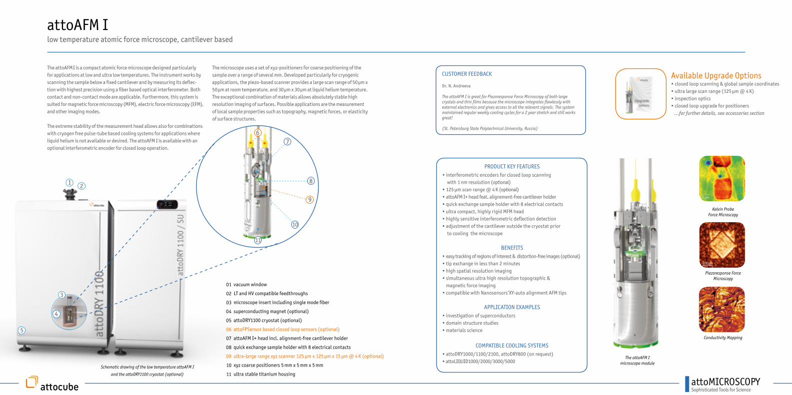
attoAFM I low temperature atomic force microscope, cantilever based
The attoAFM I is a compact atomic force microscope designed particularly for applications at low and ultra low temperatures. The instrument works by scanning the sample below a fixed cantilever and by measuring its deflec-tion with highest precision using a fiber based optical interferometer. Both contact and non-contact mode are applicable. Furthermore, this system is suited for magnetic force microscopy (MFM), electric force microscopy (EFM), and other imaging modes.
The extreme stability of the measurement head allows also for combinations with cryogen free pulse-tube based cooling systems for applications where liquid helium is not available or desired. The attoAFM I is available with an optional interferometric encoder for closed loop operation.
The microscope uses a set of xyz-positioners for coarse positioning of the sample over a range of several mm. Developed particularly for cryogenic applications, the piezo-based scanner provides a large scan range of 50 µm x 50 µm at room temperature, and 30 µm x 30 µm at liquid helium temperature. The exceptional combination of materials allows absolutely stable high resolution imaging of surfaces. Possible applications are the measurement of local sample properties such as topography, magnetic forces, or elasticity of surface structures.
The attoAFM I microscope module
Conductivity Mapping
Kelvin Probe Force Microscopy
Piezoresponse Force Microscopy
PRODUCT KEY FEATURES• interferometric encoders for closed loop scanning
with 1 nm resolution (optional)• 125 μm scan range @ 4 K (optional)• attoAFM I+ head feat. alignement-free cantilever holder• quick exchange sample holder with 8 electrical contacts• ultra compact, highly rigid MFM head • highly sensitive interferometric deflection detection • adjustment of the cantilever outside the cryostat prior
to cooling the microscope
BENEFITS• easy tracking of regions of interest & distortion-free images (optional)• tip exchange in less than 2 minutes• high spatial resolution imaging • simultaneous ultra high resolution topographic &
magnetic force imaging• compatible with Nanosensors‘XY-auto alignment AFM tips
APPLICATION EXAMPLES• investigation of superconductors• domain structure studies • materials science
COMPATIBLE COOLING SYSTEMS• attoDRY1000/1100/2100, attoDRY800 (on request)• attoLIQUID1000/2000/3000/5000
6
8
9
10
11
7
1
4
2
3
5
11
vacuum window
LT and HV compatible feedthroughs
microscope insert including single mode fiber
superconducting magnet (optional)
attoDRY1100 cryostat (optional)
attoFPSensor based closed loop sensors (optional)
attoAFM I+ head incl. alignment-free cantilever holder
quick exchange sample holder with 8 electrical contacts
ultra-large range xyz scanner 125 μm x 125 μm x 15 μm @ 4 K (optional)
xyz coarse positioners 5 mm x 5 mm x 5 mm
ultra stable titanium housing
10
09
08
07
05
06
04
03
01
02
Schematic drawing of the low temperature attoAFM I
and the attoDRY1100 cryostat (optional)
Available Upgrade Options• closed loop scanning & global sample coordinates• ultra large scan range (125 μm @ 4 K)• inspection optics• closed loop upgrade for positioners ...for further details, see accessories section

attoMICROSCOPYSophisticated Tools for Science
attoAFM I+ Headfeaturing an alignement-free cantilever holder
The attoAFM I+ head features an alignment-free cantilever holder for tip exchange, and hence takes over the complete mechanical alignment of the cantilever with respect to the fiber used for deflection readout. A folding mechanism allows for easy extraction of the cantilever holder for tip exchange without dismounting the AFM head itself.
To exchange the tip, the holder is simply put into an exchange basis with a leveled platform. This enables to easily slide in and out cantilevers, thus minimizing the danger of damaging the costly and valuable tips during handling. The tip itself is held in place by a spring blade, which can be slid open and closed via another clever quick folding mechanism.
This way, the tip can be replaced within tens of seconds. During re-attachment, a guiding rod automatically centers the cantilever holder. When folding the head back into its initial parking position, the fiber end is perfectly aligned with respect to the cantilever. The desired interference pattern with ideal contrast is thus automatically achieved without any further mechanical alignment.
The attoAFM I+ head incl. the alignment-free cantilever holder is included with every attoAFM I (2” and 1” version, as well as any upgrades such as MFM, PFM, KPFM and ct-AFM), and is compatible with all commercially available XY-auto alignment AFM tips (patented technology by ).
Tip exchange in < 2 minutes! Watch the video on1. Flip the AFM head upwards. (a)2. Remove the cantilever holder. (b)3. Perform the AFM tip exchange (for details, see description of the cantilever holder on the right) 4. Once the new tip is mounted, reattach the cantilever holder: A guiding rod (c) automatically centers the cantilever holder by fixing one degree of freedom, while the fiber ferrule is still far away from any potentially harmful obstacle.5. Feed the ferrule into the cantilever holder through another guiding sleeve (d). The ferrule is protected by a soft sleeve.6. Tilt the head back into the housing – it flips conve niently and firmly into its dedicated parking position.
Done.
There is no further mechanical alignment necessary – perfectly aligned, yielding the desired interferogram used for the deflection detection of the cantilever.
d
c
b
a
MAIN ADVANTAGES
• compact design• ultra-stable• easy to use• no special tools needed• fully pre-aligned• no re-alignement needed
after cantilever exchange• electrical pin contacts included,
no wires to be detached
Quick. Intuitive. Efficient. AFM/MFM tip exchange in less than 2 minutes
1
2
Put the cantilever holder into the exchange basis.
3
4
Perform the cantilever exchange; alignment grooves on chip guarantee perfect positioning.
Slide back the spring blade. Close the holder and remove holder from the exchange basis, and insert it back into the AFM head.
attoMICROSCOPYSophisticated Tools for Science
The PFM upgrade contains
• 10 conductive AFM tips • PFM test sample • PFM factory test at room temperture and low temperature • PFM demonstration and training during the installation
Magnetic Force Microscopy (MFM)additional AFM mode upgrades
Article Art.No.
MFM upgrade 1012468
Article Art.No.
PFM upgrade 1009869
attocube logo written
into BFO by PFM
Magnetic Force Microscopy (MFM)MFM is one of the most widely used AFM techniques, and makes use of a magnetic tip to map out the z-component of the gradient of the magnetic stray field.
The MFM upgrade contains
• 10 MFM tips • MFM test sample • MFM factory test at room temperture and low temperature • MFM demonstration and training during the installation
MFM image of hard disc
Piezoresponse Force Microscopy (PFM)PFM is capable of imaging the local deformation of a multiferroic material in response to a local electric field caused by a voltage supplied to the AFM tip.
Piezoresponse Force Microscopy (PFM)additional AFM mode upgrades
Optical fiber
Dither piezo
Sample
UAC
Optical fiber
MFM cantileverDither
Sample

attoMICROSCOPYSophisticated Tools for Science
KPFM image ofAu-on-Pt pattern
Kelvin Probe Force Microscopy (KPFM)additional AFM mode upgrades
The ct-AFM upgrade contains
• Low noise current amplifier • 10 conductive tips • Ct-AFM test sample • Ct-AFM factory test at room temperture and low temperature • Ct-AFM demonstration and training during the installation
Article Art.No.
KPFM upgrade 1009977
Article Art.No.
Ct-AFM upgrade 1008504
ct-AFM on Ruthenium
Kelvin Probe Force Microscopy (KPFM)KPFM yields information about the local variations of the work function of a material with respect to the AFM tip.
The KPFM upgrade contains • KPFM software upgrade
• 10 conductive AFM tips
• KPFM test sample
• KPFM factory test at room temperture and low temperature
• KPFM demonstration and training during the installation
Conducting-tip Atomic Force Microscopy (ct-AFM)Ct-AFM allows to map out the local electric response of a sample to an applied bias voltage via the AFM tip.
Conducting-tip Atomic Force Microscopy (ct-AFM)additional AFM mode upgrades
Optical fiber
Dither piezo
SampleUAC + UDC
Sample
Optical fiber
Dither piezo
Sample
UAC
+++++
V
Sample
Sample Tip
Tip
UAC UDC
UAC
Work Function
UCPD
attoMICROSCOPYSophisticated Tools for Science
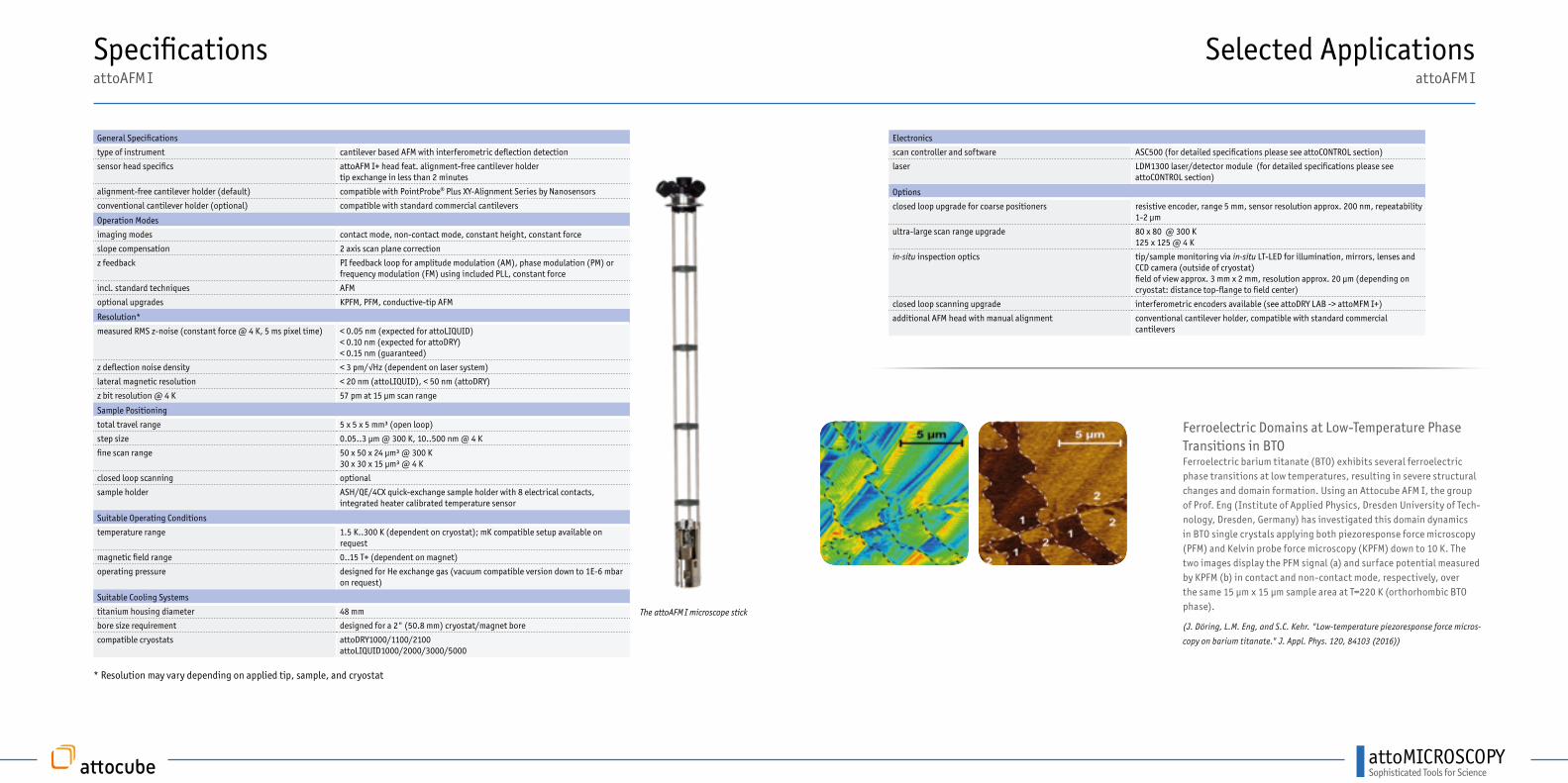
Specifications attoAFM I
The attoAFM I microscope stick
* Resolution may vary depending on applied tip, sample, and cryostat
General Specifications
type of instrument cantilever based AFM with interferometric deflection detection
sensor head specifics attoAFM I+ head feat. alignment-free cantilever holdertip exchange in less than 2 minutes
alignment-free cantilever holder (default) compatible with PointProbe® Plus XY-Alignment Series by Nanosensors
conventional cantilever holder (optional) compatible with standard commercial cantilevers
Operation Modes
imaging modes contact mode, non-contact mode, constant height, constant force
slope compensation 2 axis scan plane correction
z feedback PI feedback loop for amplitude modulation (AM), phase modulation (PM) or frequency modulation (FM) using included PLL, constant force
incl. standard techniques AFM
optional upgrades KPFM, PFM, conductive-tip AFM
Resolution*
measured RMS z-noise (constant force @ 4 K, 5 ms pixel time) < 0.05 nm (expected for attoLIQUID)< 0.10 nm (expected for attoDRY)< 0.15 nm (guaranteed)
z deflection noise density < 3 pm/√Hz (dependent on laser system)
lateral magnetic resolution < 20 nm (attoLIQUID), < 50 nm (attoDRY)
z bit resolution @ 4 K 57 pm at 15 μm scan range
Sample Positioning
total travel range 5 x 5 x 5 mm³ (open loop)
step size 0.05..3 μm @ 300 K, 10..500 nm @ 4 K
fine scan range 50 x 50 x 24 μm³ @ 300 K30 x 30 x 15 μm³ @ 4 K
closed loop scanning optional
sample holder ASH/QE/4CX quick-exchange sample holder with 8 electrical contacts, integrated heater calibrated temperature sensor
Suitable Operating Conditions
temperature range 1.5 K..300 K (dependent on cryostat); mK compatible setup available on request
magnetic field range 0..15 T+ (dependent on magnet)
operating pressure designed for He exchange gas (vacuum compatible version down to 1E-6 mbar on request)
Suitable Cooling Systems
titanium housing diameter 48 mm
bore size requirement designed for a 2" (50.8 mm) cryostat/magnet bore
compatible cryostats attoDRY1000/1100/2100attoLIQUID1000/2000/3000/5000
Electronics
scan controller and software ASC500 (for detailed specifications please see attoCONTROL section)
laser LDM1300 laser/detector module (for detailed specifications please see attoCONTROL section)
Options
closed loop upgrade for coarse positioners resistive encoder, range 5 mm, sensor resolution approx. 200 nm, repeatability 1-2 μm
ultra-large scan range upgrade 80 x 80 @ 300 K 125 x 125 @ 4 K
in-situ inspection optics tip/sample monitoring via in-situ LT-LED for illumination, mirrors, lenses and CCD camera (outside of cryostat)field of view approx. 3 mm x 2 mm, resolution approx. 20 µm (depending on cryostat: distance top-flange to field center)
closed loop scanning upgrade interferometric encoders available (see attoDRY LAB -> attoMFM I+)
additional AFM head with manual alignment conventional cantilever holder, compatible with standard commercial cantilevers
Ferroelectric Domains at Low-Temperature Phase Transitions in BTOFerroelectric barium titanate (BTO) exhibits several ferroelectric phase transitions at low temperatures, resulting in severe structural changes and domain formation. Using an Attocube AFM I, the group of Prof. Eng (Institute of Applied Physics, Dresden University of Tech-nology, Dresden, Germany) has investigated this domain dynamics in BTO single crystals applying both piezoresponse force microscopy (PFM) and Kelvin probe force microscopy (KPFM) down to 10 K. The two images display the PFM signal (a) and surface potential measured by KPFM (b) in contact and non-contact mode, respectively, over the same 15 µm x 15 µm sample area at T=220 K (orthorhombic BTO phase).
(J. Döring, L.M. Eng, and S.C. Kehr. "Low-temperature piezoresponse force micros-
copy on barium titanate." J. Appl. Phys. 120, 84103 (2016))
Selected Applications attoAFM I
attoMICROSCOPYSophisticated Tools for Science
1µm
5µm
atto
AFM
/MFM
I+
Selected Applications attoAFM I
1µm1µm
5µm
Selected Applications attoAFM I
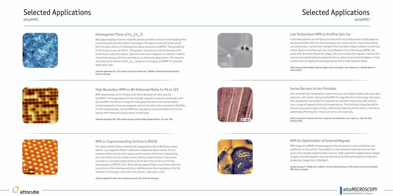
MFM for Optimization of Sintered MagnetsMFM image of a NdFeB sintered magnet with the nominal c-axis orientation per-pendicular to the surface. The sample is in the remanent state but some surface grains show already magnetization reversal. High resolution imaging allows deeper insights into the magnetic reversal mechanism and the optimization of magnetic properties. Image size is 30x30µm².
(Image courtesy of T. Helbig and O. Gutfleisch, Functional Materials Group, TU Darmstadt, Germany and Fraunhofer IWKS Hanau, Germany.)
Vortex Barriers in Iron Pnictides Iron-pnictide high-temperature superconductors are widely studied, but many open questions still remain. Using an attoAFM I for magnetic force microscopy, the group of O. Auslaender has studied twin boundaries and their interaction with vortices over a range of magnetic fields and temperatures. They find that stripes parallel to the twin boundaries repel vortices, effectively hindering vortex motion, and hence potentially affecting the critical current in such materials.
[Data courtesy of O. Auslaender (Technion, Israel); for more information, see A. Yagil et al., Phys. Rev. B 94, 064510 (2016)]
Low Temperature MFM on Artifical Spin IceFrustrated systems are intriguing for physicists since they possess highly degener-ate ground states with non-zero entropy at 0 K, which can give rise to interesting new phenomena. A prominent example which has been widely studied in condensed matter physics is artifical spin ice. Using Magnetic Force Microscopy (MFM), the group of W. Branford (Imperial College, UK) have studied the magnetic reversal of a nanostructured permalloy honeycomb lattice, demonstrating the breakdown of the artifical spin ice regime at low temperatures and in high magnetic fields.
[Data courtesy of W.R. Branford, Imperial College, UK; for more details, see K. Zeissler et al., Scientific Reports 6, 30218 (2016)]
MFM on Superconducting Vortices in BSCCOThis measurement shows a dominantly hexagonally ordered Abrikosov votex lattice, at a magnetic field of -40 Oe (the sample was field-cooled). The ori-entation of the vortices with respect to the moment of the tip is indicated by the color of the vortices: Bright colors indicate repulsive forces. The tip was scanned in a constant height of about 30 nm above the surface of a freshly cleaved piece of BSCCO-2212. Note that the applied field is much lower than the coercitivity of the hardmagnetic tip (≈ 400 Oe),hence the orientation of the tip moment is unchanged. Scan size is 10 x 10 μm², color span is 2 Hz.
(attocube applications labs, 2013; sample courtesy of A. Erb, TU Munich, Germany)
High Resolution MFM on Bit Patterned Media Co-Pd at 10 KMFM measurement on Co-Pd dots with 50 nm diameter at 10 K using the attoMFM I. The image demonstrates the high magnetic resolution achievable with the attoMFM. Variations in magnetic field perpendicular to the surface allows switching domains from one magnetic state to the other (here recorded at 6250 Oe). For this measurement, the attoMFM was operated at constant height with the fre-quency shift measured using a phase-locked loop.
(attocube application labs, 2010; sample courtesy of Hitachi Global Storage Solutions, San Jose, USA)
Helimagnetic Phase of Fe0.5Co0.5SiReal space imaging of exotic magnetic phases provides a level of understanding that cannot be achieved with indirect techniques. The figure on the left shows one of the first observations of a helimagnetic phase using the attoMFM I. The periodicity of the stripes is around 100 nm. This phase is of particular interest because of its proximity to a skyrmion phase. Skyrmions are exotic magnetic excitations, studied extensively because of their potential use in spintronic applications. The measure-ment was performed on a FeCo0.5Si0.5 sample at 4 K using an attoMFM I in attocube application labs.
(attocube application labs, 2013; sample courtesy of A. Bauer and C. Pfleiderer, Technical University of Munich, Garching, Germany)
attoMICROSCOPYSophisticated Tools for Science
2 µm
Selected ApplicationsattoAFM I
Selected Applications attoAFM I
2 µm
1µm
1µm
Kelvin Probe Force Microscopy of Au-on-Pt PatternThe measurements shown here were performed on a test sample consisting of a Au layer on a Pt substrate in dual pass mode. The KPFM image was recorded during the second line with a lift height of about 50 nm. The color scale spans approximately 130 mV, and the image size is 11.9 µm x 11.9 µm.
We found a KPFM contrast of approx. 35 mV, and a KPFM resolution (noise level) of approx. 2.6 mV.
(attocube application labs 2014)
Conductive-Tip AFM Measurements on RutheniumIn this application, atomic steps on Ruthenium were investigated using con-ductive-tip AFM. Atomic steps as well as spiral dislocations can be identified on the molecular beam epitaxy-grown sample. The contrast in this measure-ment is highly enhanced due to a difference in conductance between edges and flat plateaus. Such high contrast was not observed in the accompanying topographic image. A voltage of +10 mV was applied to the standard Pt-coated AFM tip, while the sample was grounded via a current amplifier with gain 106 V/A. The measurement was performed at room temperature in a 20 mbar He atmosphere.
(Sample and measurement courtesy of V. Da Costa, J.-F. Dayen, B. Doudin, IPCMS-DMONS,CNRS/University of Strasbourg, France)
Low Temperature Piezoresponse Force Microscopy on BiFeOPiezoresponse Force Microscopy (PFM) is a standard tool at room temperature to investigate new materials, especially multiferroics. However in many cases the scientifically interesting phases only exist at low temperatures or high magnetic fields, what demands the extension of this technique to extreme conditions. In collaboration with our customers, we adapted our attoAFM based on the general purpose ASC500 for PFM measurements. In the measurements here we investigated BiFeO3 a well know room temperature multiferroic. The figure shows piezoresponse amplitude after a box in the box writing at 160 K on the sample.
(attocube application labs, 2013; Sample courtesy of Neus Domingo & Gustau Catalan, CIN2 Barcelona, Centre d’Investigació en Nanociència i Nanotecnologia, Bellaterra, Spain)
MFM on Co Doped Mn2Sb Single CrystalMagnetic domain structure in the ferrimagnetic state of Co doped Mn2Sb single crystal imaged using an attoAFM Ixs Magnetic Force Microscopy (here at 290 K). The image was taken in constant distance mode with the height above the sam-ple surface set to 50 nm. The area shown in the figure corresponds to 15µm x 15µm with a size of 800 x 800 pixel.
(Image courtesy of Rajeev Rawat, UGC-DAE Consortium for Scientific Research, Indore, India)
Local Conductivity Mapping and PFM on BFO Thin FilmIn this application, the versatility of the attoAFM I was demonstrated on an ultra-thin film of BFO. A simple box writing and reading measurements was per-formed. During the writing phase, a DC voltage of -10 V was applied to write a box. During the reading, a 5 Vpp AC excitation at ~42 kHz on top of a -2 V DC voltage was used. Using both AC and DC voltage at the same time allows for a simultaneous measurement of PFM (right image) and local conductivity (left image).
(attocube application labs, 2014; sample courtesy of N. Domingo, ICN Barcelona, Spain)
Piezoresponse Force Image on BFOThis image shows the attocube logo electrically written into a BaFeO3 substrate next to natural domains of the sample. The data were taken at 4K in piezoresponse force mode using an attoAFM/MFM I. Image size is 5x5µm².
(attocube application labs, 2014; Sample courtesy of Marin Alexe, Functional Materials Group, Department of Physics, University of Warwick, Coventry, UK)

attoMICROSCOPYSophisticated Tools for Science
The attoSHPM+ is a compact scanning Hall probe microscope, designed particularly for operation at low temperature and high magnetic fields. At the heart of the attoSHPM+, a molecular beam epitaxy (MBE) grown GaAs/AlGaAs Hall sensor measures magnetic fields with unrivalled sensitivity. Local measurements of the magnetization of a sample are obtained by scanning the sample underneath the Hall sensor and simultaneously recording the Hall voltage, directly yielding the local magnetic stray field.
While other local probes may outperform the Hall sensor with respect to its lateral resolution, its ability to non-invasively obtain quantitative values for the local magnetic field makes the Hall sensor a unique tool for the study of superconductors and magnetic materials. The attoSHPM+ features an interferometric encoder for closed loop operation with 1 nm resolution, and an ultra large range scanner with 125 µm scan range at 4 K.
Schematic drawing of the low temperature attoSHPM
and the attoDRY1100 cryostat (optional)
The attoSHPM microscope module
PRODUCT KEY FEATURES• interferometric encoders for closed loop scanning
with 1 nm resolution• 125 μm scan range @ 4 K• quick exchange sample holder with 8 electrical contacts• STM distance tracking for conductive samples• high spatial resolution: 250 nm & 400 nm sensors available• noise-equivalent magnetic field: 15 nT/√Hz @ 4 K (40 µA Hall
current)• typ. attainable field detection limit: 15 µT (bandwidth 10 Hz @
277 Hz)• (ultra-) large cryogenic scan range: 30 µm x 30 µm x 15 µm @ 4 K
(incl.) 125 µm x 125 µm x 15 µm @ 4 K (optional)
BENEFITS• easy tracking of regions of interest & distortion-free images• gain quantitative & non-invasive magnetic information• ultra-high field sensitivity combined with sub-micron resolution• easily identify and relocalize regions of interest (ROIs) on your
sample• fits standard cryogenic and magnet sample spaces• compatible with high magnetic fields
APPLICATION EXAMPLES• vortex distribution and pinning measurements in pnicitdes,
cuprates and other superconductors• local field measurements on magnetic nanoparticles, bit patterned
media, and other materials• local hysteresis and susceptibility measurements
COMPATIBLE COOLING SYSTEMS• attoDRY1000/1100/2100• attoLIQUID1000/2000/3000, attoLIQUID5000 (on request)
Magnetic DomainImaging
Vortex Imaging
6
8
9
10
11
7
1
4
2
3
5
vacuum window
LT and HV compatible feedthroughs
microscope insert
superconducting magnet (optional)
attoDRY1100 cryostat (optional)
attoFPSensor based closed loop sensors
SHPM sensor (250 nm or 400 nm)
quick exchange sample holder with 8 electrical contacts
ultra-large range xyz scanner 125 μm x 125 μm x 15 μm @ 4 K
xyz coarse positioners 5 mm x 5 mm x 5 mm
ultra stable titanium housing
10
09
08
07
05
06
04
03
01
02
atto
SHPM
atto
SHPM
Available Upgrade Options• closed loop scanning & global sample coordinates• ultra large scan range (125 μm @ 4 K)• inspection optics• closed loop upgrade for positioners ...for further details, see accessories section
attoSHPMlow temperature scanning Hall probe microscope
attoMICROSCOPYSophisticated Tools for Science
Specifications attoSHPM
* Resolution may vary depending on applied tip, sample, and cryostat
General Specifications
type of instrument Scanning Hall Probe Microscope with STM tip for tip-sample distance control
sensor head specifics MBE grown hall cross sensor (GaAs/AlGaAs heterostructure) on a 2-axis tiltable sensor mount
Operation Modes
imaging modes constant height
slope compensation 2 axis scan plane correction
z feedback STM distance tracking (usually only for autoapproach)
Resolution*
size of Hall cross on sensor 400 nm (high resolution); 250 mm (ultra high resolution)
field sensitivity @ 4 K 1500 V/AT
noise-equivalent magnetic field (theoretical) 15 nT/√Hz @ 4 K and 40 μA Hall current80 nT/√Hz @ 77 K and 40 μA Hall current
typical attainable field detection limit (measured) 15 μT typ. (bandwith 10 Hz @ frequency 277 Hz)
z bit resolution @ 4 K 57 pm at 15 μm scan range
Sample Positioning
total travel range 5 x 5 x 5 mm³ (open loop)
step size 0.05..3 μm @ 300 K, 10..500 nm @ 4 K
fine scan range 50 x 50 x 24 µm³ @ 300 K 30 x 30 x 15 µm³ @ 4 K
closed loop scanning optional
sample holder ASH/QE/4CX quick-exchange sample holder with 8 electrical contacts, integrated heater calibrated temperature sensor
Suitable Operating Conditions
temperature range 1.5 K..300 K (dependent on cryostat); mK compatible setup available on request
magnetic field range 0..15 T+ (dependent on magnet)
operating pressure designed for He exchange gas (vacuum compatible version down to 1E-6 mbar on request)
Suitable Cooling Systems
titanium housing diameter 48 mm
bore size requirement designed for a 2" (50.8 mm) cryostat/magnet bore
compatible cryostats attoDRY1000/1100/2100attoLIQUID1000/2000/3000/5000
Electronics
scan controller and software ASC500 (for detailed specifications please see attoCONTROL section)
Options
closed loop scanning & global sample coordinates interferometric encoders for scan linearization and closed loop sample navigation
ultra-large scan range upgrade 80 x 80 @ 300 K 125 x 125 @ 4 K
in-situ inspection optics tip/sample monitoring via in-situ LT-LED for illumination, mirrors, lenses and CCD camera (outside of cryostat)field of view approx. 3 mm x 2 mm, resolution approx. 20 µm (depending on cryostat: distance top-flange to field center
closed loop upgrade for coarse positioners resistive encoder, range 5 mm, sensor resolution approx. 200 nm, repeatability 1-2 µm
Selected ApplicationsattoSHPM
2 µm
Vortex Imaging via Scanning Hall Probe MicroscopySHPM measurements on a degraded Bi2Sr2CaCu2O8+x substrate have been performed demonstrating strong surface pinning effects at 4.2 K and 2.5 Gauss external magnetic field. The figure shows the vortex distribu-tion measured in constant height of approx. 100 nm above the surface.
(attocube applications labs, 2011; sample courtesy of A. Erb, TU Munich, Germany)
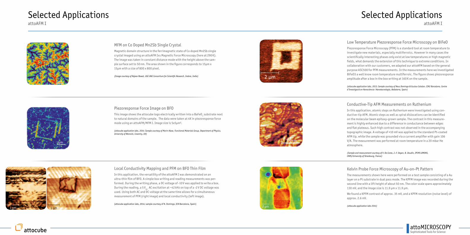
Domain Imaging in BaFeOThe 15 µm x 15 µm sized image shows a sample of BaFeO recorded with an attoSHPM, recorded at 4.2 K. The SHPM sensor was kept in a constant height of about 200 nm. The color scale spans 106 mT (dark to bright), while the S/N ratio of this measurement yields an exceptional 50 000:1. Note that SHPM records absolute field strength as opposed to MFM tech-niques, that record only field gradients.
(attocube application labs, 2011; sample courtesy of R. Kramer, Institut Néel, CNRS, Grenoble)

attoMICROSCOPYSophisticated Tools for Science
attoAFM IIItuning fork based, low temperature atomic force microscope
The attoAFM III is an atomic force microscope designed partic-ularly for applications at low and ultra low temperature. Due to the non-optical shear force detection based on a tuning fork, this system is ideally suited for applications where input of light is problematic. A typical application of the attoAFM III microscope is scanning gate microscopy (SGM) on semiconductor structures. This microscope is compatible with the commercially available tuning fork tips, and is available with optional interferometric encoder for closed loop scanning.
The attoAFM III uses a tuning fork sensor as detection mechanism for the tip-sample forces, allowing high resolution non-contact mode imaging without the need for any optical deflection detection techniques. An AFM tip is glued onto one prong of a small quartz tuning fork, which is then excited to oscillate in horizontal direc-tion. The decrease in amplitude due to tip-sample interaction when approaching the sample is monitored and/or used as a feedback sig-nal. The force resolution of this technique is typically 0.1 pN.
PRODUCT KEY FEATURES• ultra compact AFM head with unprecedented stability• interferometric encoders for closed loop scanning (optional)• highly sensitive, non-optical tuning fork sensor• large cryogenic scan range:
30 µm x 30 µm x 2 µm @ 4 K
BENEFITS• ultra high resolution imaging in non-contact mode• high Q factor for high sensitivity measurements• optimized S/N ratio due to LT compatible preamplifier• no optical alignment necessary
APPLICATION EXAMPLES• materials science: ultra-high resolution topographic imaging• scanning gate microscopy at mK temperatures• investigations of semiconductor structures
COMPATIBLE COOLING SYSTEMS• attoDRY 1000/11000/2100• attoLIQUID1000/2000/3000/5000
The attoAFM III microscope module
Scanning GateMicroscopy
High resolution AFM
Kelvin Probe Force Microscopy
CUSTOMER FEEDBACK
Dr. Stefan Heun
Directly after the set up in our labs, the attoAFM III in a 3He cryostat - used for scanning gate microscopy experiments - has started to produce great data for us. It runs more than 5 years now, and we have published several papers since then. The instrument worked within specifications from the first day and we really appreciate the excellent attocube support throughout the years.
(Istituto Nanoscienze-CNR and Scuola Normale Superiore, Pisa, Italy)
Schematic drawing of the low temperature
attoAFM III and the surrounding liquid
helium dewar (optional)
1
2
3
4
5
67
8
9
10
01 LT and HV compatible feedthroughs
02 vacuum window
03 microscope insert
04 superconducting magnet (optional)
05 liquid He dewar (optional)
06 ultra stable Titanium housing
07 xyz coarse positioners
08 xyz scanner
09 quick-exchange sample holder
10 tuning fork AFM sensor
Available Upgrade Options• closed loop scanning & global sample coordinates• ultra large scan range (125 μm @ 4 K)• inspection optics• closed loop upgrade for positioners ...for further details, see accessories section

attoMICROSCOPYSophisticated Tools for Science
The attoAFM III microscope stick
Specifications attoAFM III
* Resolution may vary depending on applied tip, sample, and cryostat
General Specifications
type of instrument tuning-fork based AFM with shear-force or standard detection
sensor head specifics etched metal wires, etched or pulled optical fiber probes, STM tips, Akiyama probes(also compatible with NaugaNeedles commercial tips)
Operation Modes
imaging modes non-contact mode AFM, EFM, SGM
slope compensation 2 axis scan plane correction
z feedback PI feedback loop for amplitude modulation (AM), phase modulation (PM) or frequency modulation (FM) using included PLL
optional upgrades AFM/STM mode
Resolution*
measured z-noise density < 16 pm/√Hz
z bit resolution @ 4 K 7.6 pm at 2 μm scan range
Sample Positioning
total travel range 5 x 5 x 5 mm³ (open loop)
step size 0.05..3 μm @ 300 K, 10..500 nm @ 4 K
fine scan range 50 x 50 x 4.2 μm³ @ 300 K30 x 30 x 2 μm³ @ 4 K
sample holder ASH/QE/0 quick exchange sample holder and integrated heater with calibrated temperature sensor
Suitable Operating Conditions
temperature range 1.5 K..300 K (dependent on cryostat); mK compatible setup available on request
magnetic field range 0..15 T+ (dependent on magnet)
operating pressure designed for He exchange gas (vacuum compatible version down to 1E-6 mbar on request)
Suitable Cooling Systems
titanium housing diameter 48 mm
bore size requirement designed for a 2" (50.8 mm) cryostat/magnet bore
compatible cryostats attoDRY1000/1100/2100attoLIQUID1000/2000/3000/5000
Electronics
scan controller and software ASC500 (for detailed specifications please see attoCONTROL section)
Options
sample holder upgrade ASH/QE/4CX quick-exchange sample holder with 8 electrical contacts and integrated heater with calibrated temperature sensor
closed loop upgrade for coarse positioners resistive encoder, range 5 mm, sensor resolution approx. 200 nm, repeatability 1-2 μm
ultra-large scan range upgrade 80 x 80 @ 300 K 125 x 125 @ 4 K
in-situ inspection optics tip/sample monitoring via in-situ LT-LED for illumination, mirrors, lenses and CCD camera (outside of cryostat)field of view approx. 3 mm x 2 mm, resolution approx. 20 μm (depending on cryostat: distance top-flange to field center)
closed loop scanning upgrade interferometric encoders available
Selected ApplicationsattoAFM III
Imaging Fractional Incompressible Stripes in Quantum Hall SystemsIn newer measurements, the group performed SGM measurements at the temperature and magnetic field conditions required to observe the fractional quantum Hall ef-fect. The goal is to image for the first time the presence of fractional incompressible stripes, i.e. the existence of an inner structure within the integer edge channel. The measurements were performed at bulk filling factor n = 1 (B = 8.23 T, T = 300 mK). The corresponding SGM map in the region close to the QPC center is depicted in the lower Figure (a). Analogously to the n = 4 case, one expects to find plateaus when the local electron phase is gapped, i.e. when the local filling factor n*equals a robust fraction. The scan profile depicted in the right figure reveals a clear shoulder for G
sd = e2/3h
(corresponding to points where n* = 1/3). A more careful analysis [1] allows to deter-mine the occurrence of incompressible phases for n* = 1/3, 2/5, 2/3, and 3/5, i.e. the two most robust fractions and their hole-particle conjugates, respectively. The SGM maps allow not only to reveal the fractional incompressible stripes, but also to mea-sure their width and correlate it with the local electron density slope. The agreement between the data and a reconstruction model is remarkable, especially in light of the uncertainty on the fractional-gap value, which is known to be rather sensitive to the details of disorder potential.
(Data and images were generously provided by N. Paradiso, S. Heun et al., NEST, CNR-INFM and Scuola Normale Superiore, Pisa, Italy.)[1] N. Paradiso et al., Phys. Rev. Lett. 108, 246801 (2012). See also the Supplemental Material.
Scanning Gate Microscopy at 300 mKIn this measurement, an attoAFM III was operated inside an attoLIQUID3000 cryo-stat at 300 mK in scanning gate microscopy mode (SGM) - investigating the trajectory and interaction of edge channels of a split-gate quantum point contact (QPC) device in the Quantum Hall (QH) regime. By scanning the SGM tip over the surface of the QPC at constant height and by simultaneously measuring and plotting the source-drain current, conductance maps were obtained. The image to the left is an example of such a conductance map depicting the characteristic branched-flow of electrons at zero magnetic field, which in turn shows electron interference fringes and the actual electron path (T = 400 mK, 2DEG density n2D = 3.37 x 1011 cm-2).
(Data and images were generously provided by S. Heun et al., NEST, CNR-INFM and Scuola Normale Superiore, Pisa, Italy.)

attoMICROSCOPYSophisticated Tools for Science
01 LT and HV compatible feedthroughs
02 vacuum window
03 microscope insert
04 superconducting magnet (optional)
05 liquid He dewar (optional)
06 confocal microscope objective
07 AFM Akiyama probe
08 two xyz coarse positioners and xyz scanner units
09 ultra stable Titanium housing
Schematic drawing of the low temperature attoAFM/CFM and the surrounding liquid Helium dewar (optional)
The tuning fork based attoAFM/CFM not only allows fast optical inves-tigation of the sample prior to detailed AFM studies, it also enables precise positioning of the AFM tip over small structures and optical control of the scanning process or any surface manipulation. Also, op-tical experiments such as Raman spectroscopy and tip enhanced Raman spectroscopy (TERS) can be conducted. Needless to say that all of these tasks can be performed in extreme environments, such as ultra low tem-perature, high vacuum and magnetic fields.
The attoAFM/CFM uses an Akiyama probe tip to investigate tip-sample in-teraction forces on the nanometer scale. The Akiyama probe is typical-
ly operated in non-contact mode using a phase-locked loop to excite the probe at resonance and track any shift in frequency due to tip-sam-ple interactions. An additional PI controller keeps the frequency shift at a constant value while scanning over the surface. Simultaneously to the information provided by the Akiyama probe, the CFM reveals complementary optical information of the sam-ple surface. Since the z-scanning motion is provided by a dedicated scanner on the side of the AFM, the focal distance between the low-temperature compatible lens and the sample does not change.
1
2
3
5
4
7
6
8
PRODUCT KEY FEATURES• scan area at 4 K: 12 x 12 µm²• independent sample scanning and scanning of the AFM
module• tuning fork based and PLL controlled systems available• non contact measurement mode• objectives with various working distances available
BENEFITS• suitable for conducting and non-conducting samples• enables exact positioning of AFM tip• optical access to the sample with high magnification
APPLICATION EXAMPLES• solid state physics and quantum dot optics• fluorescence observation• highly stable long term experiments on single quantum dots
COMPATIBLE COOLING SYSTEMS • attoDRY1000/1100/2100, attoDRY800(on request)• attoLIQUID1000/2000, attoLIQUID3000/5000 (on request)
The attoAFM /CFM
microscope module
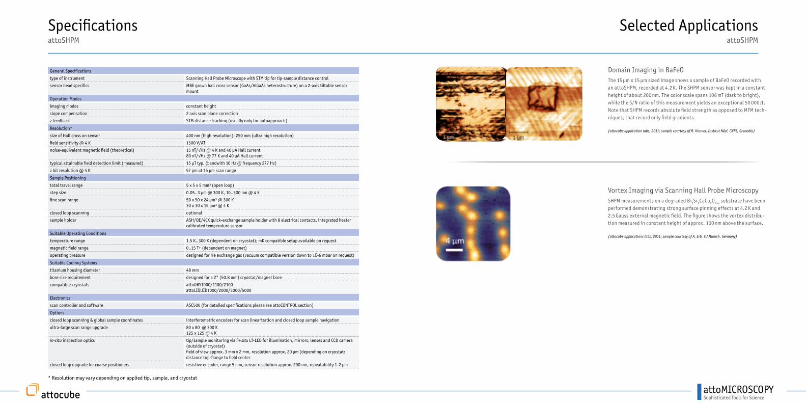
Principle of atomic-sized magnetic sensors using NV centers.
Tip EnhancedRaman Spectroscopy
Color Centersin Diamond
Magnetic DomainImaging
CUSTOMER FEEDBACK
Prof. Dr. Patrick Maletinsky
Our attoLIQUID1000-based attoAFM/CFM system was a completegame-changer for starting up my research group. Instead of spending years developing a highly complex technical system on our own, we had a fully operational, high-performance cryogenic AFM/CFM system at hand within a relatively short timespan. This allowed us to plunge into our scientific endea-vours with highest efficiency. As always, this attocube product stands out due to its reliability, ease of use and excellent performance. A particular further asset is the systems versatility - interfacing it with our existing experiments was straight-forward due to the clever system design and excellent support from attocube‘s application engineers.
(Department of Physics, University of Basel, Switzerland)
CUSTOMER FEEDBACK
Prof. Dr. Vincent Jacques
Owing to the high stability and easy operation of the attoAFM/CFM, we were able to perform first magnetometry experiments within only a few months. Support from attocube engineers was always very prompt and efficient. The system is now operated since two years and I must say that it has been the cornerstone of the rapid development of scanning probe magnetometry in our group.
(LPQM, ENS-Cachan, France)
9
Available Upgrade Option• closed loop scanning
& global sample coordinates ...for further details, see accessories section
attoAFM/CFM combined low temperature atomic force and confocal microscope, tuning fork based
attoMICROSCOPYSophisticated Tools for Science
Specifications attoAFM/CFM
Selected ApplicationsattoAFM/CFM
* Resolution may vary depending on applied tip, sample, and cryostat
General Specifications
type of instrument combined confocal (CFM) and atomic force microscope (AFM)
sensor head specifics AFM: Akiyama probe (quartz tuning fork combined with a mircomachined cantilever)CFM: attoCFM I external optics head and low temperature apochromatic
Operation Modes
imaging modes optically detected magnetic resonance (ODMR), AFM, CFM
slope compensation 2 axis scan plane correction
z feedback AFM: PI feedback loop for amplitude modulation (AM), phase modulation (PM) or frequency modulation (FM) using included PLL
Resolution*
measured RMS z-noise (constant force @ 4 K, 5 ms pixel time) < 0.2 nm (expected for attoLIQUID1000)< 0.5 nm (guaranteed for attoLIQUID1000)
z bit resolution @ 4 K 7.6 pm at 2 μm scan range
Confocal Unit
configuration compact and modular design, two or more optical channelsstandard configuration: 1 excitation channel,1 detection channel
quick-exchange of optical components beamsplitters, filter mounts for up to 4 filters/ polarizers (1" diameter), optional piezoelectric rotator with filter mount
LT- compatible objective LT-APO/VIS, LT-APO/VISIR, LT-APO/NIR(see accessory section for more information)
inspection unit sample imaging with large field of view: ~75 μm (attoDRY), ~56 μm (attoLIQUID)
Illumination
excitation wavelength range 400 .. 1000 nmdefault: 650 nm (others on request)
Detection
detection mode e.g. optically detected magnetic resonance (ODMR), luminescence, fluorescence
Sample Positioning
total travel range independent degrees of freedom for tip and sample of 2 mm x 3 mm x 2.5 mm (closed loop)
step size 0.05..3 μm @ 300 K, 10..500 nm @ 4 K
fine scan range 30 μm x 30 μm x 4.3 μm @ 300 K, 12 μm x 12 μm x 2 μm @ 4 K (open loop)
sample holder Ti plate with integrated heater and calibrated temperature sensor
Suitable Operating Conditions
temperature range 1.5 K..300 K (dependent on cryostat); mK compatible setup available on request
magnetic field range 0..15 T+ (dependent on magnet)
operating pressure designed for He exchange gas (vacuum compatible version down to 1E-6 mbar on request)
Suitable Cooling Systems
titanium housing diameter 48 mm
bore size requirement designed for a 2" (50.8 mm) cryostat/magnet bore
compatible cryostats attoLIQUID1000/2000(attoLIQUID3000/5000 & attoDRY1000/1100/2000 on request)
Electronics
scan controller and software ASC500 (for detailed specifications please see attoCONTROL section)
laser LDM600 laser/detector module (for detailed specifications please see attoCONTROL section)
References:
[1] L. Rondin et al., Appl. Phys. Lett. 100, 153118 (2012)
Related publications based on the attoAFM/CFM (2012-2016)
[2] L. Thiel et al., Nature Nanotechnology (2016), doi:10.1038/nnano.2016.63[3] Tetienne et al ., Science 344, 1366 (2014)[4] J.-P. Tetienne et al., Nature Communications 6, 6733 (2015)[5] A. Dréau et al., Phys. Rev. Lett. 113, 137601 (2014)[6] A. Dréau et al., Phys. Rev. Lett. 110, 060502 (2013)[7] L. Rondin et al., Nature communications 4, 2279 (2013)[8] J.-P. Tetienne et al., Phys. Rev. B 87, 235436 (2013)[9] J.-P. Tetienne et al., New J. Phys. 14, 103033 (2012)[10] A. Dréau et al., Phys. Rev. B 85, 134107 (2012) [11] L. Rondin et al., Appl. Phys. Lett. 100, 153118 (2012)
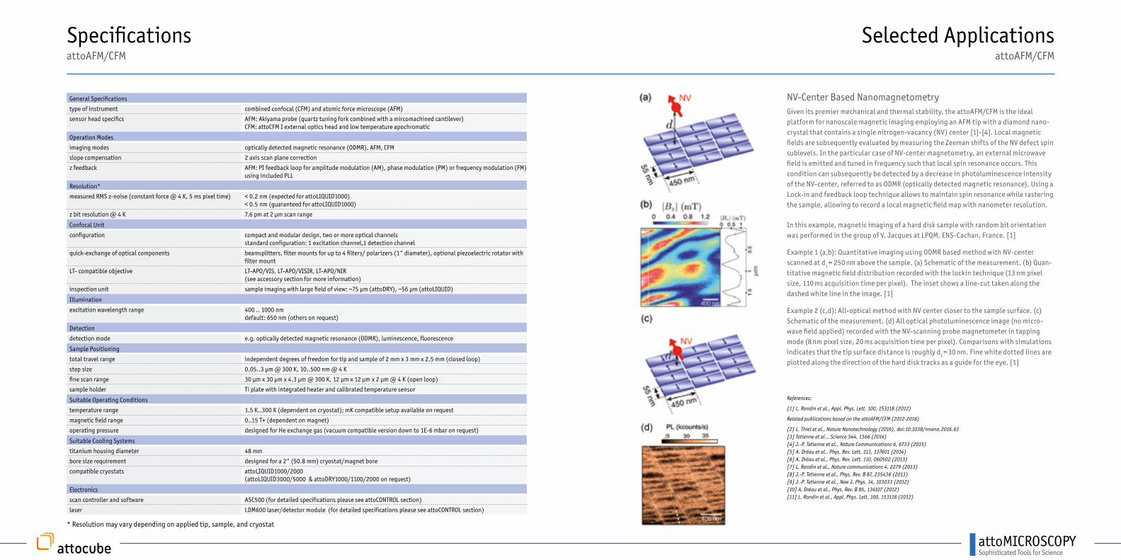
NV-Center Based NanomagnetometryGiven its premier mechanical and thermal stability, the attoAFM/CFM is the ideal platform for nanoscale magnetic imaging employing an AFM tip with a diamond nano-crystal that contains a single nitrogen-vacancy (NV) center [1]-[4]. Local magnetic fields are subsequently evaluated by measuring the Zeeman shifts of the NV defect spin sublevels. In the particular case of NV-center magnetometry, an external microwave field is emitted and tuned in frequency such that local spin resonance occurs. This condition can subsequently be detected by a decrease in photoluminescence intensity of the NV-center, referred to as ODMR (optically detected magnetic resonance). Using a Lock-in and feedback loop technique allows to maintain spin resonance while rastering the sample, allowing to record a local magnetic field map with nanometer resolution.
In this example, magnetic imaging of a hard disk sample with random bit orientation was performed in the group of V. Jacques at LPQM, ENS-Cachan, France. [1]
Example 1 (a,b): Quantitative imaging using ODMR based method with NV-center scanned at d1 = 250 nm above the sample. (a) Schematic of the measurement. (b) Quan-titative magnetic field distribution recorded with the lockin technique (13 nm pixel size, 110 ms acquisition time per pixel). The inset shows a line-cut taken along the dashed white line in the image. [1]
Example 2 (c,d): All-optical method with NV center closer to the sample surface. (c) Schematic of the measurement. (d) All optical photoluminescence image (no micro-wave field applied) recorded with the NV-scanning probe magnetometer in tapping mode (8 nm pixel size, 20 ms acquisition time per pixel). Comparisons with simulations indicates that the tip surface distance is roughly d2 = 30 nm. Fine white dotted lines are plotted along the direction of the hard disk tracks as a guide for the eye. [1]
attoMICROSCOPYSophisticated Tools for Science
Selected ApplicationsattoAFM/CFM
Selected ApplicationsattoAFM/CFM
Images courtesy of V. Jacques, University of Montpellier, FR; for more details, see Tetienne et al ., “Nanoscale imaging and control of domain-wall hopping with a NV center microscope”, Science 344, 1366(2014)
atto
AFM
/CF
M
atto
AFM
/CF
M
Images courtesy of P. Maletinsky, University of Basel, CH; for more details, see L. Thiel et al., “Quantitative nanoscale vortex imaging using a cryogenic quantum magnetometer”, Nature Nanotechnology (2016), doi:10.1038/nnano.2016.63
Nanoscale Imaging and Control of Domain-Wall HoppingDomain walls in magnetic wires may prove useful for future spintronic devices, and hence their nanoscale characterization is an important steps towards useful applications. As demonstrated by the group of Vincent Jaques in Science, their NV center microscope based on the attoAFM/CFM allows to image domain walls in a 1 nm thick ferromagnetic nanowire with high resolution as well as jumps between pinning sites of individual domain walls. At the same time, they showed that the domain walls can be moved along the wire by in-ducing jumps via local heating due to a high local laser power. Since the domain walls are pinned by nearest pinning site, this allows to probe and image the pinning landscape of the sample quite efficiently.
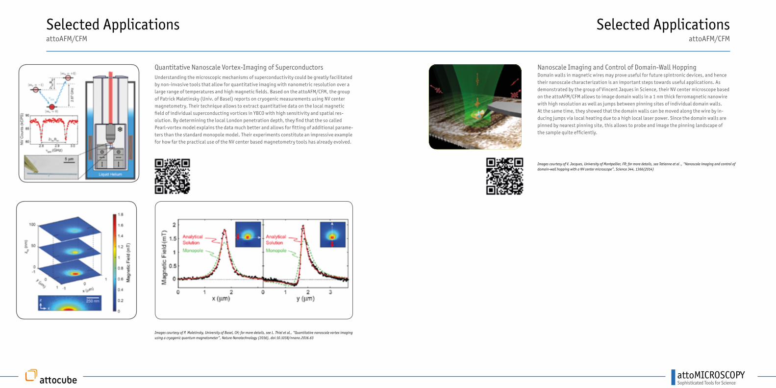
Quantitative Nanoscale Vortex-Imaging of SuperconductorsUnderstanding the microscopic mechanisms of superconductivity could be greatly facilitated by non-invasive tools that allow for quantitative imaging with nanometric resolution over a large range of temperatures and high magnetic fields. Based on the attoAFM/CFM, the group of Patrick Maletinsky (Univ. of Basel) reports on cryogenic measurements using NV center magnetometry. Their technique allows to extract quantitative data on the local magnetic field of individual superconducting vortices in YBCO with high sensitivity and spatial res-olution. By determining the local London penetration depth, they find that the so called Pearl-vortex model explains the data much better and allows for fitting of additional parame-ters than the standard monopole model. Their experiments constitute an impressive example for how far the practical use of the NV center based magnetometry tools has already evolved.