attiny261 attiny461 attiny861 automotive preliminary summary
TRANSCRIPT

8-bit Microcontroller with 2/4/8K Bytes In-SystemProgrammable Flash
ATtiny261ATtiny461ATtiny861
Automotive
Preliminary
Summary
7753BS–AVR–08/08
BDTIC www.bdtic.com/ATMEL
Features• High Performance, Low Power AVR® 8-Bit Microcontroller• Advanced RISC Architecture
– 123 Powerful Instructions – Most Single Clock Cycle Execution– 32 x 8 General Purpose Working Registers– Fully Static Operation
• Non-volatile Program and Data Memories– 2/4/8K Byte of In-System Programmable Program Memory Flash
(ATtiny261/461/861)Endurance: 10,000 Write/Erase Cycles
– 128/256/512 Bytes In-System Programmable EEPROM (ATtiny261/461/861)Endurance: 100,000 Write/Erase Cycles
– 128/256/512 Bytes Internal SRAM (ATtiny261/461/861)– Programming Lock for Self-Programming Flash Program and EEPROM Data
Security• Peripheral Features
– 8/16-bit Timer/Counter with Prescaler– 8/10-bit High Speed Timer/Counter with Separate Prescaler
3 High Frequency PWM Outputs with Separate Output Compare RegistersProgrammable Dead Time Generator
– Universal Serial Interface with Start Condition Detector– 10-bit ADC
11 Single Ended Channels16 Differential ADC Channel Pairs15 Differential ADC Channel Pairs with Programmable Gain (1x, 8x, 20x, 32x)
– Programmable Watchdog Timer with Separate On-chip Oscillator– On-chip Analog Comparator
• Special Microcontroller Features– debugWIRE On-chip Debug System– In-System Programmable via SPI Port– External and Internal Interrupt Sources– Low Power Idle, ADC Noise Reduction, and Power-down Modes– Enhanced Power-on Reset Circuit– Programmable Brown-out Detection Circuit– Internal Calibrated Oscillator
• I/O and Packages– 16 Programmable I/O Lines– 20-pin SOIC, 32-pad MLF and 20-lead TSSOP
• Operating Voltage:– 2.7 - 5.5V for ATtiny261/461/861
• Speed Grade:– ATtiny261/461/861: 0 - 8 MHz @ 2.7 - 5.5V, 0 - 16 MHz @ 4.5 - 5.5V– Operating temperature: Automotive (-40°C to +125°C)
• Low Power Consumption– Active Mode: 1 MHz, 2.7V: 380μA– Power-down Mode: 0.1μA at 2.7V

1. Pin Configurations
Figure 1-1. Pinout ATtiny261/461/861
Note: The large center pad underneath the QFN/MLF package should be soldered to ground on the board to ensure good mechanical stability.
12345678910
20191817161514131211
(MOSI/DI/SDA/OC1A/PCINT8) PB0 (MISO/DO/OC1A/PCINT9) PB1
(SCK/USCK/SCL/OC1B/PCINT10) PB2(OC1B/PCINT11) PB3
VCCGND
(ADC7/OC1D/CLKI/XTAL1/PCINT12) PB4(ADC8/OC1D/CLKO/XTAL2/PCINT13) PB5
(ADC9/INT0/T0/PCINT14) PB6 (ADC10/RESET/PCINT15) PB7
PA0 (ADC0/DI/SDA/PCINT0)PA1 (ADC1/DO/PCINT1) PA2 (ADC2/INT1/USCK/SCL/PCINT2)PA3 (AREF/PCINT3)AGNDAVCCPA4 (ADC3/ICP0/PCINT4)PA5 (ADC4/AIN2/PCINT5)PA6 (ADC5/AIN0/PCINT6)PA7 (ADC6/AIN1/PCINT7)
SOIC / TSSOP
12345678
2423222120191817
32 31 30 29 28 27 26 25
9 10 11 12 13 14 15 16
NC(OC1B/PCINT11) PB3
NCVCC
GNDNC
(ADC7/OC1D/CLKI/XTAL1/PCINT12) PB4(ADC8/OC1D/CLKO/XTAL2/PCINT13) PB5
NCPA2 (ADC2/INT1/USCK/SCL/PCINT2)PA3 (AREF/PCINT3)AGNDNCNCAVCCPA4 (ADC3/ICP0/PCINT4)
NC
(AD
C9/
INT0
/T0/
PCIN
T14)
PB6
(AD
C10
/RES
ET/P
CIN
T15)
PB7 N
C(A
DC
6/A
IN1/
PCIN
T7) P
A7
(AD
C5/
AIN
0/PC
INT6
) PA
6(A
DC
4/A
IN2/
PCIN
T5) P
A5
NC
PB2
(SC
K/U
SCK/
SCL/
OC
1B/P
CIN
T10)
PB1
(MIS
O/D
O/O
C1A
/PC
INT9
)PB
0 (M
OSI
/DI/
SDA
/OC
1A/P
CIN
T8)
NC
NC
NC
PA0
(AD
C0/
DI/
SDA
/PC
INT0
)PA
1 (A
DC
1/D
O/P
CIN
T1)
QFN/MLF
27753BS–AVR–08/08
ATtiny261/461/861
ATtiny261/461/861
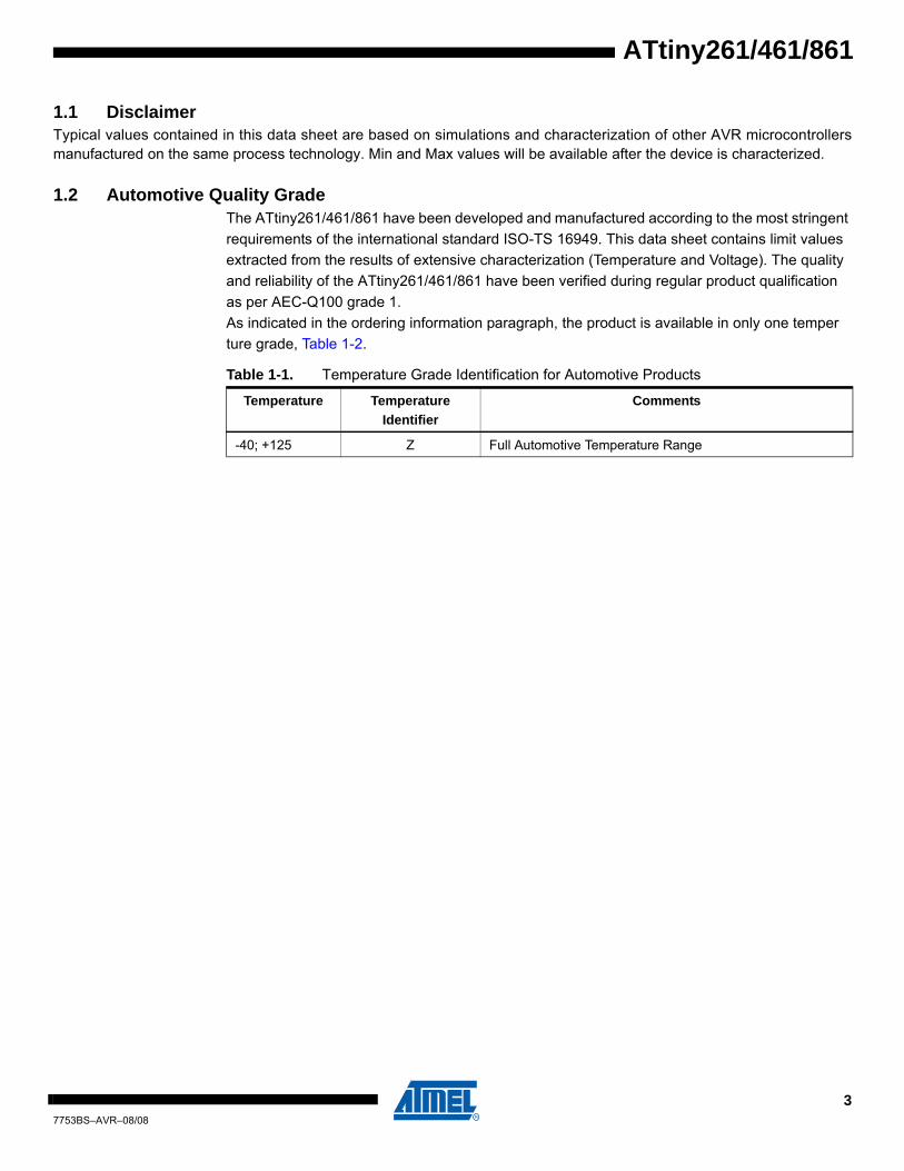
1.1 DisclaimerTypical values contained in this data sheet are based on simulations and characterization of other AVR microcontrollersmanufactured on the same process technology. Min and Max values will be available after the device is characterized.
1.2 Automotive Quality GradeThe ATtiny261/461/861 have been developed and manufactured according to the most stringent requirements of the international standard ISO-TS 16949. This data sheet contains limit values extracted from the results of extensive characterization (Temperature and Voltage). The quality and reliability of the ATtiny261/461/861 have been verified during regular product qualification as per AEC-Q100 grade 1. As indicated in the ordering information paragraph, the product is available in only one temper ture grade, Table 1-2.
Table 1-1. Temperature Grade Identification for Automotive Products
Temperature TemperatureIdentifier
Comments
-40; +125 Z Full Automotive Temperature Range
37753BS–AVR–08/08

2. OverviewThe ATtiny261/461/861 is a low-power CMOS 8-bit microcontroller based on the AVR enhancedRISC architecture. By executing powerful instructions in a single clock cycle, theATtiny261/461/861 achieves throughputs approaching 1 MIPS per MHz allowing the systemdesigner to optimize power consumption versus processing speed.
2.1 Block Diagram
Figure 2-1. Block Diagram
PORT A (8)PORT B (8)
USI
Timer/Counter1Timer/Counter0 A/D Conv.
InternalBandgap
Analog Comp.
SRAMFlash
EEPROM
WatchdogOscillator
WatchdogTimer
OscillatorCircuits /
ClockGeneration
PowerSupervisionPOR / BOD &
RESET
VC
C
GN
D
PROGRAMLOGIC
debugWIRE
AGND
AREF
AVCC
DAT
AB
US
PA[0..7]PB[0..7]
11
RESETXTAL[1..2]
CPU
3
47753BS–AVR–08/08
ATtiny261/461/861
ATtiny261/461/861
The AVR core combines a rich instruction set with 32 general purpose working registers. All the32 registers are directly connected to the Arithmetic Logic Unit (ALU), allowing two independentregisters to be accessed in one single instruction executed in one clock cycle. The resultingarchitecture is more code efficient while achieving throughputs up to ten times faster than con-ventional CISC microcontrollers.
The ATtiny261/461/861 provides the following features: 2/4/8K byte of In-System ProgrammableFlash, 128/256/512 bytes EEPROM, 128/256/512 bytes SRAM, 6 general purpose I/O lines, 32general purpose working registers, one 8-bit Timer/Counter with compare modes, one 8-bit highspeed Timer/Counter, Universal Serial Interface, Internal and External Interrupts, a 4-channel,10-bit ADC, a programmable Watchdog Timer with internal Oscillator, and three software select-able power saving modes. The Idle mode stops the CPU while allowing the SRAM,Timer/Counter, ADC, Analog Comparator, and Interrupt system to continue functioning. ThePower-down mode saves the register contents, disabling all chip functions until the next Inter-rupt or Hardware Reset. The ADC Noise Reduction mode stops the CPU and all I/O modulesexcept ADC, to minimize switching noise during ADC conversions.
The device is manufactured using Atmel’s high density non-volatile memory technology. TheOn-chip ISP Flash allows the Program memory to be re-programmed In-System through an SPIserial interface, by a conventional non-volatile memory programmer or by an On-chip boot coderunning on the AVR core.
The ATtiny261/461/861 AVR is supported with a full suite of program and system developmenttools including: C Compilers, Macro Assemblers, Program Debugger/Simulators, In-Circuit Emu-lators, and Evaluation kits.
57753BS–AVR–08/08

3. Instruction Set SummaryMnemonics Operands Description Operation Flags #Clocks
ARITHMETIC AND LOGIC INSTRUCTIONSADD Rd, Rr Add two Registers Rd ← Rd + Rr Z,C,N,V,H 1ADC Rd, Rr Add with Carry two Registers Rd ← Rd + Rr + C Z,C,N,V,H 1ADIW Rdl,K Add Immediate to Word Rdh:Rdl ← Rdh:Rdl + K Z,C,N,V,S 2SUB Rd, Rr Subtract two Registers Rd ← Rd - Rr Z,C,N,V,H 1SUBI Rd, K Subtract Constant from Register Rd ← Rd - K Z,C,N,V,H 1SBC Rd, Rr Subtract with Carry two Registers Rd ← Rd - Rr - C Z,C,N,V,H 1SBCI Rd, K Subtract with Carry Constant from Reg. Rd ← Rd - K - C Z,C,N,V,H 1SBIW Rdl,K Subtract Immediate from Word Rdh:Rdl ← Rdh:Rdl - K Z,C,N,V,S 2AND Rd, Rr Logical AND Registers Rd ← Rd • Rr Z,N,V 1ANDI Rd, K Logical AND Register and Constant Rd ← Rd • K Z,N,V 1OR Rd, Rr Logical OR Registers Rd ← Rd v Rr Z,N,V 1ORI Rd, K Logical OR Register and Constant Rd ← Rd v K Z,N,V 1EOR Rd, Rr Exclusive OR Registers Rd ← Rd ⊕ Rr Z,N,V 1COM Rd One’s Complement Rd ← 0xFF − Rd Z,C,N,V 1NEG Rd Two’s Complement Rd ← 0x00 − Rd Z,C,N,V,H 1SBR Rd,K Set Bit(s) in Register Rd ← Rd v K Z,N,V 1CBR Rd,K Clear Bit(s) in Register Rd ← Rd • (0xFF - K) Z,N,V 1INC Rd Increment Rd ← Rd + 1 Z,N,V 1DEC Rd Decrement Rd ← Rd − 1 Z,N,V 1TST Rd Test for Zero or Minus Rd ← Rd • Rd Z,N,V 1CLR Rd Clear Register Rd ← Rd ⊕ Rd Z,N,V 1SER Rd Set Register Rd ← 0xFF None 1BRANCH INSTRUCTIONSRJMP k Relative Jump PC ← PC + k + 1 None 2IJMP Indirect Jump to (Z) PC ← Z None 2RCALL k Relative Subroutine Call PC ← PC + k + 1 None 3ICALL Indirect Call to (Z) PC ← Z None 3RET Subroutine Return PC ← STACK None 4RETI Interrupt Return PC ← STACK I 4CPSE Rd,Rr Compare, Skip if Equal if (Rd = Rr) PC ← PC + 2 or 3 None 1/2/3CP Rd,Rr Compare Rd − Rr Z, N,V,C,H 1 CPC Rd,Rr Compare with Carry Rd − Rr − C Z, N,V,C,H 1CPI Rd,K Compare Register with Immediate Rd − K Z, N,V,C,H 1SBRC Rr, b Skip if Bit in Register Cleared if (Rr(b)=0) PC ← PC + 2 or 3 None 1/2/3SBRS Rr, b Skip if Bit in Register is Set if (Rr(b)=1) PC ← PC + 2 or 3 None 1/2/3SBIC P, b Skip if Bit in I/O Register Cleared if (P(b)=0) PC ← PC + 2 or 3 None 1/2/3SBIS P, b Skip if Bit in I/O Register is Set if (P(b)=1) PC ← PC + 2 or 3 None 1/2/3BRBS s, k Branch if Status Flag Set if (SREG(s) = 1) then PC←PC+k + 1 None 1/2BRBC s, k Branch if Status Flag Cleared if (SREG(s) = 0) then PC←PC+k + 1 None 1/2BREQ k Branch if Equal if (Z = 1) then PC ← PC + k + 1 None 1/2BRNE k Branch if Not Equal if (Z = 0) then PC ← PC + k + 1 None 1/2BRCS k Branch if Carry Set if (C = 1) then PC ← PC + k + 1 None 1/2BRCC k Branch if Carry Cleared if (C = 0) then PC ← PC + k + 1 None 1/2BRSH k Branch if Same or Higher if (C = 0) then PC ← PC + k + 1 None 1/2BRLO k Branch if Lower if (C = 1) then PC ← PC + k + 1 None 1/2BRMI k Branch if Minus if (N = 1) then PC ← PC + k + 1 None 1/2BRPL k Branch if Plus if (N = 0) then PC ← PC + k + 1 None 1/2BRGE k Branch if Greater or Equal, Signed if (N ⊕ V= 0) then PC ← PC + k + 1 None 1/2BRLT k Branch if Less Than Zero, Signed if (N ⊕ V= 1) then PC ← PC + k + 1 None 1/2BRHS k Branch if Half Carry Flag Set if (H = 1) then PC ← PC + k + 1 None 1/2BRHC k Branch if Half Carry Flag Cleared if (H = 0) then PC ← PC + k + 1 None 1/2BRTS k Branch if T Flag Set if (T = 1) then PC ← PC + k + 1 None 1/2BRTC k Branch if T Flag Cleared if (T = 0) then PC ← PC + k + 1 None 1/2BRVS k Branch if Overflow Flag is Set if (V = 1) then PC ← PC + k + 1 None 1/2BRVC k Branch if Overflow Flag is Cleared if (V = 0) then PC ← PC + k + 1 None 1/2BRIE k Branch if Interrupt Enabled if ( I = 1) then PC ← PC + k + 1 None 1/2BRID k Branch if Interrupt Disabled if ( I = 0) then PC ← PC + k + 1 None 1/2BIT AND BIT-TEST INSTRUCTIONSSBI P,b Set Bit in I/O Register I/O(P,b) ← 1 None 2CBI P,b Clear Bit in I/O Register I/O(P,b) ← 0 None 2LSL Rd Logical Shift Left Rd(n+1) ← Rd(n), Rd(0) ← 0 Z,C,N,V 1LSR Rd Logical Shift Right Rd(n) ← Rd(n+1), Rd(7) ← 0 Z,C,N,V 1ROL Rd Rotate Left Through Carry Rd(0)←C,Rd(n+1)← Rd(n),C←Rd(7) Z,C,N,V 1
67753BS–AVR–08/08
ATtiny261/461/861

ATtiny261/461/861
ROR Rd Rotate Right Through Carry Rd(7)←C,Rd(n)← Rd(n+1),C←Rd(0) Z,C,N,V 1ASR Rd Arithmetic Shift Right Rd(n) ← Rd(n+1), n=0..6 Z,C,N,V 1SWAP Rd Swap Nibbles Rd(3..0)←Rd(7..4),Rd(7..4)←Rd(3..0) None 1BSET s Flag Set SREG(s) ← 1 SREG(s) 1BCLR s Flag Clear SREG(s) ← 0 SREG(s) 1BST Rr, b Bit Store from Register to T T ← Rr(b) T 1BLD Rd, b Bit load from T to Register Rd(b) ← T None 1SEC Set Carry C ← 1 C 1CLC Clear Carry C ← 0 C 1SEN Set Negative Flag N ← 1 N 1CLN Clear Negative Flag N ← 0 N 1SEZ Set Zero Flag Z ← 1 Z 1CLZ Clear Zero Flag Z ← 0 Z 1SEI Global Interrupt Enable I ← 1 I 1CLI Global Interrupt Disable I ← 0 I 1SES Set Signed Test Flag S ← 1 S 1CLS Clear Signed Test Flag S ← 0 S 1SEV Set Twos Complement Overflow. V ← 1 V 1CLV Clear Twos Complement Overflow V ← 0 V 1SET Set T in SREG T ← 1 T 1CLT Clear T in SREG T ← 0 T 1SEH Set Half Carry Flag in SREG H ← 1 H 1CLH Clear Half Carry Flag in SREG H ← 0 H 1DATA TRANSFER INSTRUCTIONSMOV Rd, Rr Move Between Registers Rd ← Rr None 1MOVW Rd, Rr Copy Register Word Rd+1:Rd ← Rr+1:Rr None 1LDI Rd, K Load Immediate Rd ← K None 1LD Rd, X Load Indirect Rd ← (X) None 2LD Rd, X+ Load Indirect and Post-Inc. Rd ← (X), X ← X + 1 None 2LD Rd, - X Load Indirect and Pre-Dec. X ← X - 1, Rd ← (X) None 2LD Rd, Y Load Indirect Rd ← (Y) None 2LD Rd, Y+ Load Indirect and Post-Inc. Rd ← (Y), Y ← Y + 1 None 2LD Rd, - Y Load Indirect and Pre-Dec. Y ← Y - 1, Rd ← (Y) None 2LDD Rd,Y+q Load Indirect with Displacement Rd ← (Y + q) None 2LD Rd, Z Load Indirect Rd ← (Z) None 2LD Rd, Z+ Load Indirect and Post-Inc. Rd ← (Z), Z ← Z+1 None 2LD Rd, -Z Load Indirect and Pre-Dec. Z ← Z - 1, Rd ← (Z) None 2LDD Rd, Z+q Load Indirect with Displacement Rd ← (Z + q) None 2LDS Rd, k Load Direct from SRAM Rd ← (k) None 2ST X, Rr Store Indirect (X) ← Rr None 2ST X+, Rr Store Indirect and Post-Inc. (X) ← Rr, X ← X + 1 None 2ST - X, Rr Store Indirect and Pre-Dec. X ← X - 1, (X) ← Rr None 2ST Y, Rr Store Indirect (Y) ← Rr None 2ST Y+, Rr Store Indirect and Post-Inc. (Y) ← Rr, Y ← Y + 1 None 2ST - Y, Rr Store Indirect and Pre-Dec. Y ← Y - 1, (Y) ← Rr None 2STD Y+q,Rr Store Indirect with Displacement (Y + q) ← Rr None 2ST Z, Rr Store Indirect (Z) ← Rr None 2ST Z+, Rr Store Indirect and Post-Inc. (Z) ← Rr, Z ← Z + 1 None 2ST -Z, Rr Store Indirect and Pre-Dec. Z ← Z - 1, (Z) ← Rr None 2STD Z+q,Rr Store Indirect with Displacement (Z + q) ← Rr None 2STS k, Rr Store Direct to SRAM (k) ← Rr None 2LPM Load Program Memory R0 ← (Z) None 3LPM Rd, Z Load Program Memory Rd ← (Z) None 3LPM Rd, Z+ Load Program Memory and Post-Inc Rd ← (Z), Z ← Z+1 None 3SPM Store Program Memory (z) ← R1:R0 NoneIN Rd, P In Port Rd ← P None 1OUT P, Rr Out Port P ← Rr None 1PUSH Rr Push Register on Stack STACK ← Rr None 2POP Rd Pop Register from Stack Rd ← STACK None 2MCU CONTROL INSTRUCTIONSNOP No Operation None 1SLEEP Sleep (see specific descr. for Sleep function) None 1WDR Watchdog Reset (see specific descr. for WDR/Timer) None 1BREAK Break For On-chip Debug Only None N/A
Mnemonics Operands Description Operation Flags #Clocks
77753BS–AVR–08/08

4. Ordering InformationTable 4-1. Engineering Samples Delivery only
Table 4-2. Available Product Offering
Notes: 1. This device can also be supplied in wafer form. Please contact your local Atmel sales office for detailed ordering information and minimum quantities.
2. Pb-free packaging, complies to the European Directive for Restriction of Hazardous Substances (RoHS directive). Also Halide free and fully Green.
3. For Speed vs. VCC,see Figure 23.3 on page 189
Ordering Code(2) Speed (MHz)(3) Power Supply (V) Package(1) Operation Range
ATtiny261-ESSZ 16 2.7 - 5.5 TG Automotive (-40° to +125°C)
ATtiny261-ESMZ 16 2.7 - 5.5 PN Automotive (-40° to +125°C)
ATtiny261-ESXZ 16 2.7 - 5.5 6G Automotive (-40° to +125°C)
ATtiny461-ESSZ 16 2.7 - 5.5 TG Automotive (-40° to +125°C)
ATtiny461-ESMZ 16 2.7 - 5.5 PN Automotive (-40° to +125°C)
ATtiny461-ESXZ 16 2.7 - 5.5 6G Automotive (-40° to +125°C)
ATtiny861-ESSZ 16 2.7 - 5.5 TG Automotive (-40° to +125°C)
ATtiny861-ESMZ 16 2.7 - 5.5 PN Automotive (-40° to +125°C)
ATtiny861-ESXZ 16 2.7 - 5.5 6G Automotive (-40° to +125°C)
Ordering Code(2) Speed (MHz)(3) Power Supply (V) Package(1) Operation Range
ATtiny261-15SZ 16 2.7 - 5.5 TG Automotive (-40° to +125°C)
ATtiny261-15MZ 16 2.7 - 5.5 PN Automotive (-40° to +125°C)
ATtiny261-15XZ 16 2.7 - 5.5 6G Automotive (-40° to +125°C)
ATtiny461-15SZ 16 2.7 - 5.5 TG Automotive (-40° to +125°C)
ATtiny461-15MZ 16 2.7 - 5.5 PN Automotive (-40° to +125°C)
ATtiny461-15XZ 16 2.7 - 5.5 6G Automotive (-40° to +125°C)
ATtiny861-15SZ 16 2.7 - 5.5 TG Automotive (-40° to +125°C)
ATtiny861-15MZ 16 2.7 - 5.5 PN Automotive (-40° to +125°C)
ATtiny861-15XZ 16 2.7 - 5.5 6G Automotive (-40° to +125°C)
87753BS–AVR–08/08
ATtiny261/461/861

ATtiny261/461/861
Package Type
PN 32-pad, 5.0 x 5.0 mm Body, Lead Pitch 0.50 mm, Quad Flat No Lead Package (QFN)
TG 20-lead, 0.300" Wide Body Lead, Plastic Gull Wing Small Outline Package (SOIC)
6G20-leads, 4.4x6.5mm body - 0.65mm Pitch - Lead Length: 0.6mmThin Shrink Small Outline Package (TSSOP)
97753BS–AVR–08/08

5. Packaging Information
5.1 PN
107753BS–AVR–08/08
ATtiny261/461/861

ATtiny261/461/861
5.2 TG
117753BS–AVR–08/08

127753BS–AVR–08/08
ATtiny261/461/861

ATtiny261/461/861
5.3 6G
137753BS–AVR–08/08

6. Errata
6.1 Errata ATtiny261The revision letter in this section refers to the revision of the ATtiny261 device.
6.1.1 Rev ANo known errata.
6.2 Errata ATtiny461The revision letter in this section refers to the revision of the ATtiny461 device.
6.2.1 Rev BNo known errata.
6.3 Errata ATtiny861The revision letter in this section refers to the revision of the ATtiny861 device.
6.3.1 Rev BNo known errata.
147753BS–AVR–08/08
ATtiny261/461/861
ATtiny261/461/861
7. Datasheet Revision History
7.1 Rev. 7753A – 11/07
7.2 Rev. 7753B – 08/08
1. First Datasheet Draft - Initial Automotive Version. Started from Industrial Datasheetdoc2588 rev.B - 01/07
1. Added 6G product offering to Ordering Information.
157753BS–AVR–08/08

Headquarters International
Atmel Corporation2325 Orchard ParkwaySan Jose, CA 95131USATel: 1(408) 441-0311Fax: 1(408) 487-2600
Atmel AsiaRoom 1219Chinachem Golden Plaza77 Mody Road TsimshatsuiEast KowloonHong KongTel: (852) 2721-9778Fax: (852) 2722-1369
Atmel EuropeLe Krebs8, Rue Jean-Pierre TimbaudBP 30978054 Saint-Quentin-en-Yvelines CedexFranceTel: (33) 1-30-60-70-00 Fax: (33) 1-30-60-71-11
Atmel Japan9F, Tonetsu Shinkawa Bldg.1-24-8 ShinkawaChuo-ku, Tokyo 104-0033JapanTel: (81) 3-3523-3551Fax: (81) 3-3523-7581
Product Contact
Web Sitewww.atmel.com
Technical [email protected]
Sales Contactwww.atmel.com/contacts
Literature Requestswww.atmel.com/literature
Disclaimer: The information in this document is provided in connection with Atmel products. No license, express or implied, by estoppel or otherwise, to anyintellectual property right is granted by this document or in connection with the sale of Atmel products. EXCEPT AS SET FORTH IN ATMEL’S TERMS AND CONDI-TIONS OF SALE LOCATED ON ATMEL’S WEB SITE, ATMEL ASSUMES NO LIABILITY WHATSOEVER AND DISCLAIMS ANY EXPRESS, IMPLIED OR STATUTORYWARRANTY RELATING TO ITS PRODUCTS INCLUDING, BUT NOT LIMITED TO, THE IMPLIED WARRANTY OF MERCHANTABILITY, FITNESS FOR A PARTICULARPURPOSE, OR NON-INFRINGEMENT. IN NO EVENT SHALL ATMEL BE LIABLE FOR ANY DIRECT, INDIRECT, CONSEQUENTIAL, PUNITIVE, SPECIAL OR INCIDEN-TAL DAMAGES (INCLUDING, WITHOUT LIMITATION, DAMAGES FOR LOSS OF PROFITS, BUSINESS INTERRUPTION, OR LOSS OF INFORMATION) ARISING OUTOF THE USE OR INABILITY TO USE THIS DOCUMENT, EVEN IF ATMEL HAS BEEN ADVISED OF THE POSSIBILITY OF SUCH DAMAGES. Atmel makes norepresentations or warranties with respect to the accuracy or completeness of the contents of this document and reserves the right to make changes to specificationsand product descriptions at any time without notice. Atmel does not make any commitment to update the information contained herein. Unless specifically providedotherwise, Atmel products are not suitable for, and shall not be used in, automotive applications. Atmel’s products are not intended, authorized, or warranted for useas components in applications intended to support or sustain life.
© 2008 Atmel Corporation. All rights reserved. Atmel®, logo and combinations thereof, and others are registered trademarks or trademarks ofAtmel Corporation or its subsidiaries. Other terms and product names may be trademarks of others.
7753BS–AVR–08/08