attenuators - admiral microwaves · attenuators general microwave pin diode attenuators cover the...
TRANSCRIPT
9
AttenuatorsGeneral Microwave PIN diode attenuators cover the frequency range from 200 MHz to 40 GHz and are available in numerous configurations to permit the user to optimize system performance. Most designs are available with either analog or digital control, operating over octave or multi-octave bands with high or moderate switching speed characteristics.
ATTENUATOR TOPOLOGYGMC PIN diode attenuators are designed with several different topologies, each of which has been selected to optimize certain performance characteristics. A brief discussion of these various topologies is presented below including a treatment of performance trade-offs.
SHUNT-MOUNTED REFLECTIVE ATTENUATORThe simplest version of a PIN diode attenuator consists of one or more PIN diodes in shunt with a transmission line as shown in Fig. 1. This design provides a broadband reflective attenuator that can reach very high levels of attenuation, depending upon the number and electrical spacing of the diodes. While it generally has very low insertion loss and can operate at high switching rates, its usefulness is limited by the very large mismatch it presents in the attenuation state.
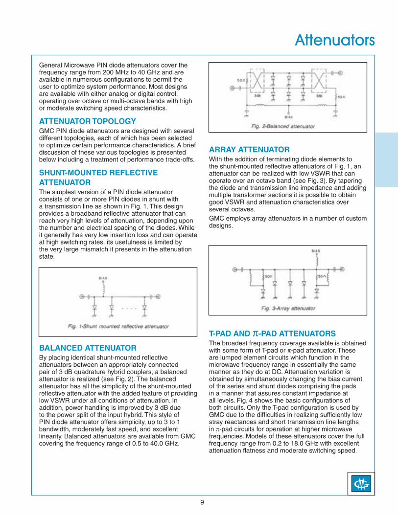
ARRAY ATTENUATORWith the addition of terminating diode elements to the shunt-mounted reflective attenuators of Fig. 1, an attenuator can be realized with low VSWR that can operate over an octave band (see Fig. 3). By tapering the diode and transmission line impedance and adding multiple transformer sections it is possible to obtain good VSWR and attenuation characteristics over several octaves.GMC employs array attenuators in a number of custom designs.
BALANCED ATTENUATORBy placing identical shunt-mounted reflective attenuators between an appropriately connected pair of 3 dB quadrature hybrid couplers, a balanced attenuator is realized (see Fig. 2). The balanced attenuator has all the simplicity of the shunt-mounted reflective attenuator with the added feature of providing low VSWR under all conditions of attenuation. In addition, power handling is improved by 3 dB due to the power split of the input hybrid. This style of PIN diode attenuator offers simplicity, up to 3 to 1 bandwidth, moderately fast speed, and excellent linearity. Balanced attenuators are available from GMC covering the frequency range of 0.5 to 40.0 GHz.
T-PAD AND π-PAD ATTENUATORSThe broadest frequency coverage available is obtained with some form of T-pad or π-pad attenuator. These are lumped element circuits which function in the microwave frequency range in essentially the same manner as they do at DC. Attenuation variation is obtained by simultaneously changing the bias current of the series and shunt diodes comprising the pads in a manner that assures constant impedance at all levels. Fig. 4 shows the basic configurations of both circuits. Only the T-pad configuration is used by GMC due to the difficulties in realizing sufficiently low stray reactances and short transmission line lengths in π-pad circuits for operation at higher microwave frequencies. Models of these attenuators cover the full frequency range from 0.2 to 18.0 GHz with excellent attenuation flatness and moderate switching speed.

10
Attenuators
SWITCHED BIT ATTENUATORSWhen an attenuator with a fast switching speed and high power handling capacity is required, the only option is to utilize a switched-bit attenuator. This attenuator combines one or more tandem pairs of SP2T switches with a zero loss connection between one pair of outputs and a fixed attenuator inserted in the other (see Fig. 5). In this configuration the PIN diodes are not used as variable resistors, but are switched between their forward and reversed biased states. This allows for much faster switching speed since high speed PIN diodes and drive circuitry can be used. In addition, it offers higher power handling capacity since the RF power is absorbed in the fixed attenuator(s), and not in the PIN diodes.There are some disadvantages to this approach that may limit its usefulness. First, the minimum practical attenuation step size at microwave frequencies is
about 0.5 dB due to interacting VSWR’s as the bits are switched. These interactions may lead to a non-monotonic response as the attenuation is changed in increments of one LSB, i.e., the attenuation level may actually decrease when an increasing attenuation step is called for. Second, because of the RF circuit complexity, the cost of this attenuator is usually higher than other approaches. Finally, the incorporation of high speed switches may lead to excess video leakage.
PHASE INVARIANT ATTENUATORSThis specialized class of attenuators has the property that the insertion phase variation is minimized as the attenuation level is changed. A unique topology is employed by GMC to obtain this performance which is described in detail in a separate technical paper.(1) In all other respects they perform in a manner similar to the balanced attenuators described above.
DRIVER CONSIDERATIONSAll attenuators except for the switched bit variety are available with linearizing driver circuits with either analog or digital control inputs. In addition, many attenuators are available without the driver for those who choose to provide their own. Most digital attenuators are available with eight-bit TTL control which, for an attenuator with a nominal attenuation range of 60 dB, will provide a resolution of 0.25 dB. Some attenuators are available with a resolution of as low as 0.05 dB. Except for switched-bit designs, all PIN diode attenuators are analog in nature and thus their resolution is essentially limited by the DAC used in the driver circuit.The driver circuit includes compensating elements to minimize the variation of attenuator with temperature. It also provides the proper source impedance and switching waveforms to optimize switching speed.
(1) “Broadband Phase Invariant Attenuator”, D. Adler and P. Maritato; 1988 IEEE MTTS Digest, pp. 673-676. To obtain a copy of this paper, please write to
SALES, HERLEY FARMINGDALE • 25 Smith St. Farmingdale, NY, 11735
11
AttenuatorsMONOTONICITYIn most applications it is imperative that the attenuator displays monotonic behavior as a function of the control input. Non-monotonic performance can occur in switched bit attenuators when interacting VSWR’s are not properly compensated, or in digitally controlled analog attenuators when a non-monotonic condition exists in the MSB of the DAC. All GMC’s attenuators are guaranteed monotonic.
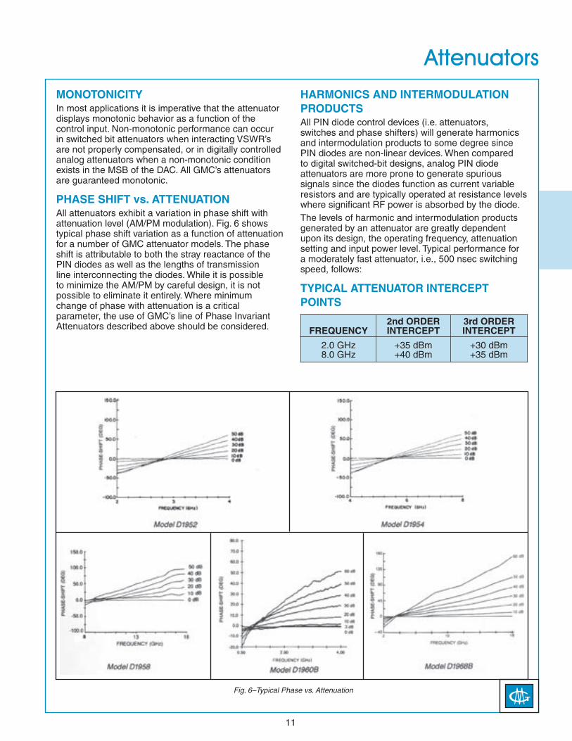
PHASE SHIFT vs. ATTENUATIONAll attenuators exhibit a variation in phase shift with attenuation level (AM/PM modulation). Fig. 6 shows typical phase shift variation as a function of attenuation for a number of GMC attenuator models. The phase shift is attributable to both the stray reactance of the PIN diodes as well as the lengths of transmission line interconnecting the diodes. While it is possible to minimize the AM/PM by careful design, it is not possible to eliminate it entirely. Where minimum change of phase with attenuation is a critical parameter, the use of GMC’s line of Phase Invariant Attenuators described above should be considered.
HARMONICS AND INTERMODULATION PRODUCTSAll PIN diode control devices (i.e. attenuators, switches and phase shifters) will generate harmonics and intermodulation products to some degree since PIN diodes are non-linear devices. When compared to digital switched-bit designs, analog PIN diode attenuators are more prone to generate spurious signals since the diodes function as current variable resistors and are typically operated at resistance levels where significant RF power is absorbed by the diode.The levels of harmonic and intermodulation products generated by an attenuator are greatly dependent upon its design, the operating frequency, attenuation setting and input power level. Typical performance for a moderately fast attenuator, i.e., 500 nsec switching speed, follows:
TYPICAL ATTENUATOR INTERCEPT POINTS
Fig. 6–Typical Phase vs. Attenuation
FREQUENCY2nd ORDER INTERCEPT
3rd ORDER INTERCEPT
2.0 GHz 8.0 GHz
+35 dBm +40 dBm
+30 dBm +35 dBm
12
AttenuatorsPOWER HANDLINGThe power handling of a PIN diode attenuator is dependent on its topology, biasing levels, and switching speed. The faster the attenuator, the lower the power handling capability. This catalog specifies both the maximum operating and the maximum survival levels. Maximum operating level is defined as that which will cause either a one dB compression of attenuation level or an out of specification condition. The survival levels are generally dependent on the maximum ratings of the semiconductors in the attenuator. Please consult the factory for special applications requiring higher operational power levels than those listed in this catalog.
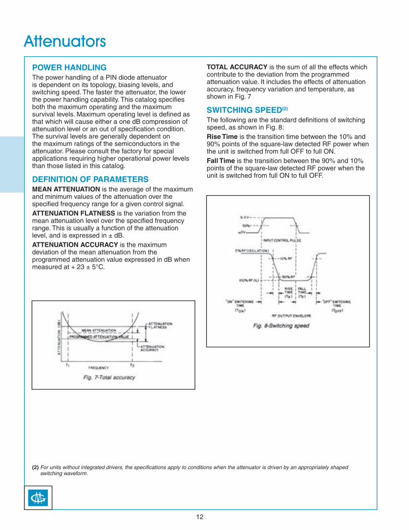
DEFINITION OF PARAMETERSMEAN ATTENUATION is the average of the maximum and minimum values of the attenuation over the specified frequency range for a given control signal.ATTENUATION FLATNESS is the variation from the mean attenuation level over the specified frequency range. This is usually a function of the attenuation level, and is expressed in ± dB.ATTENUATION ACCURACY is the maximum deviation of the mean attenuation from the programmed attenuation value expressed in dB when measured at + 23 ± 5°C.
TOTAL ACCURACY is the sum of all the effects which contribute to the deviation from the programmed attenuation value. It includes the effects of attenuation accuracy, frequency variation and temperature, as shown in Fig. 7
SWITCHING SPEED(2)
The following are the standard definitions of switching speed, as shown in Fig. 8:Rise Time is the transition time between the 10% and 90% points of the square-law detected RF power when the unit is switched from full OFF to full ON.Fall Time is the transition between the 90% and 10% points of the square-law detected RF power when the unit is switched from full ON to full OFF.
(2) For units without integrated drivers, the specifications apply to conditions when the attenuator is driven by an appropriately shaped switching waveform.

13
AttenuatorsOn Time is the transition time between 50% of the input control signal to the 90% point of the square-law detected RF power when the unit is switched from full OFF to full ON.Off Time is the transition time between 50% of the input control signal to the 10% point of the square-law detected RF power when the unit is switched from full ON to full OFF.Note: Depending on the attenuator topology, there
are differences in the behavior of the switching characteristics that may affect system performance. Switching speed is only specified to the 90% or 10% points of the detected RF signal, but the time the attenuator takes to reach final attenuation value or switch between different attenuation levels may be significantly longer.
MODULATION BANDWIDTHSmall Signal Bandwidth: With reference to a modulation frequency of 100 Hz and a modulation depth of ±3 dB at a quiescent level of −6 dB, the frequency at which the modulation depth decreases by 50% as measured with a square-law detector.Large Signal Bandwidth: With reference to a modulation frequency of 100 Hz and a 100% modulation depth at a quiescent level of −6 dB, the frequency at which the modulation depth decreases by 50% as measured with a square-law detector.TEMPERATURE COEFFICIENT is defined as the average rate of change of attenuation over the full operating temperature range of the unit under fixed bias conditions. It is expressed in dB/°C. Note that the attenuator temperature coefficient may vary with both temperature and programmed attenuation level.

14
AttenuatorSelection Guide
ATTENUATORS AND MODULATORS
FREQUENCY RANGE (GHz) ATTENUATION RANGE (dB)
MODEL PAGE COMMENTS0.2 0.5 1.0 2.0 4.0 8.0 12.4 18 40
CONTINUOUSLY VARIABLE, CURRENT CONTROLLED, ABSORPTIVE ATTENUATORS 0.5 1 60 1950A
19Single control
1 2 60 1951
2 4 60 1952
2.6 5.2 60 1953
4 8 60 1954
5 10 60 1955
6 12 60 1956
8 18 60 1958
18 40 50 1959 165
CONTINUOUSLY VARIABLE, VOLTAGE CONTROLLED, LINEARIZED ABSORPTIVE ATTENUATORS 0.5 4 60 D1960B
27
Integrated driver and RF section
0.5 8 60 D1961B
2 8 60 D1962B
2 18 60 D1968B
0.5 1 80 D1950A
23
1 2 60 D1951
2 4 60 D1952
2.6 5.2 60 D1953
4 8 60 D1954
5 10 60 D1955
6 12 60 D1956
8 18 60 D1958
18 40 50 D1959 165
VOLTAGE CONTROLLED, PHASE INVARIANT, LINEARIZED ATTENUATORS 2 6 32 D1972
30 Integrated driver and RF section 4 11 32 D1974
6 18 32 D1978
HIGH SPEED ABSORPTIVE PULSE MODULATORS
0.2 18 80 F192A 16 Integrated driver and RF section
15
AttenuatorSelection Guide (Con’t)
ATTENUATORS AND MODULATORS (con’t)
FREQUENCY RANGE (GHz) ATTENUATION RANGE (dB)
MIN STEP
SIZE (dB)MODEL PAGE COMMENTS
0.2 0.5 1.0 2.0 4.0 8.0 12.4 18 40
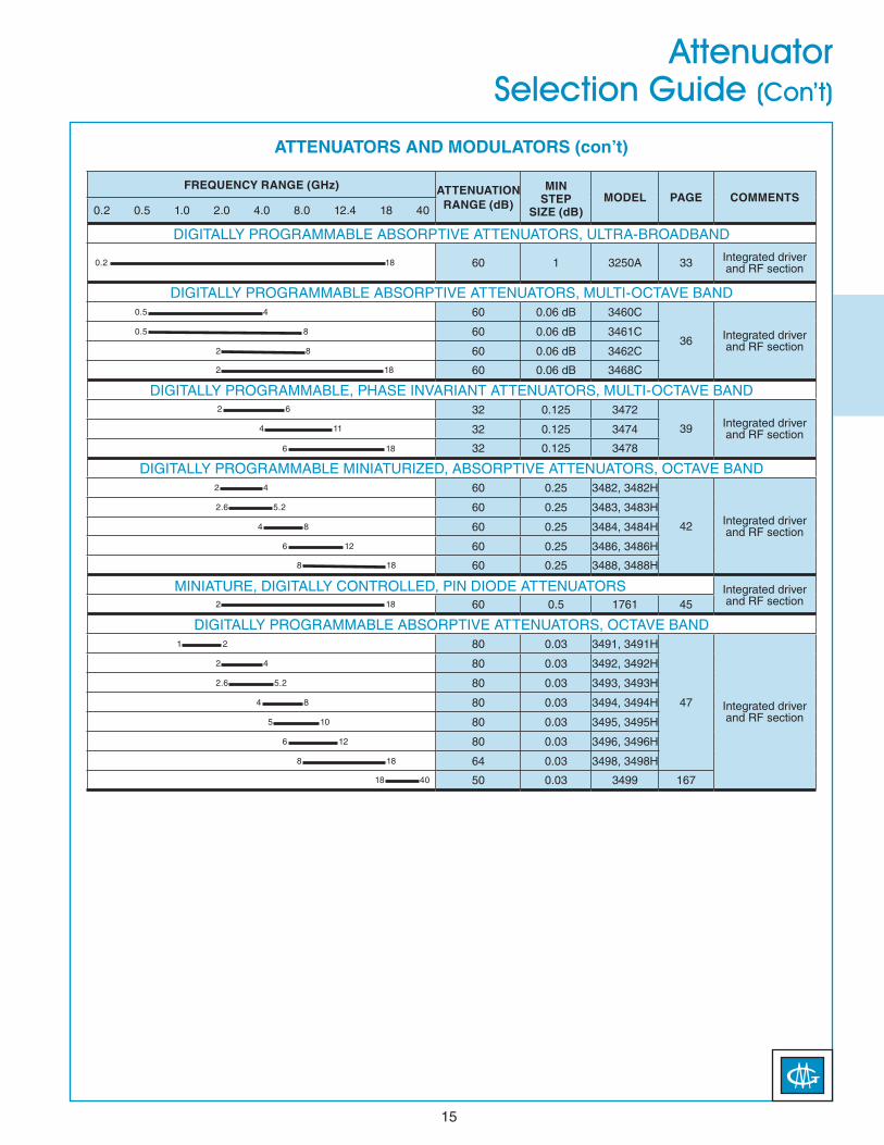
DIGITALLY PROGRAMMABLE ABSORPTIVE ATTENUATORS, ULTRA-BROADBAND
0.2 18 60 1 3250A 33 Integrated driver and RF section
DIGITALLY PROGRAMMABLE ABSORPTIVE ATTENUATORS, MULTI-OCTAVE BAND 0.5 4 60 0.06 dB 3460C
36 Integrated driver and RF section
0.5 8 60 0.06 dB 3461C
2 8 60 0.06 dB 3462C
2 18 60 0.06 dB 3468C
DIGITALLY PROGRAMMABLE, PHASE INVARIANT ATTENUATORS, MULTI-OCTAVE BAND 2 6 32 0.125 3472
39 Integrated driver and RF section
4 11 32 0.125 3474
6 18 32 0.125 3478
DIGITALLY PROGRAMMABLE MINIATURIZED, ABSORPTIVE ATTENUATORS, OCTAVE BAND 2 4 60 0.25 3482, 3482H
42 Integrated driver and RF section
2.6 5.2 60 0.25 3483, 3483H
4 8 60 0.25 3484, 3484H
6 12 60 0.25 3486, 3486H
8 18 60 0.25 3488, 3488H
MINIATURE, DIGITALLY CONTROLLED, PIN DIODE ATTENUATORS Integrated driver and RF section 2 18 60 0.5 1761 45
DIGITALLY PROGRAMMABLE ABSORPTIVE ATTENUATORS, OCTAVE BAND 1 2 80 0.03 3491, 3491H
47 Integrated driver and RF section
2 4 80 0.03 3492, 3492H
2.6 5.2 80 0.03 3493, 3493H
4 8 80 0.03 3494, 3494H
5 10 80 0.03 3495, 3495H
6 12 80 0.03 3496, 3496H
8 18 64 0.03 3498, 3498H
18 40 50 0.03 3499 167

16
Model F192A Non-ReflectiveUltra-Broadband High-Speed Pulse Modulator
• High speed • 0.2 to 18 GHz frequency range • 80 dB isolation• Low VSWR and insertion loss• Small size, light weight
The Model F192A is a high-speed non-reflective PIN diode pulse modulator with integrated driver. Operating over the instantaneous frequency range from 0.2 to 18 GHz, it provides a minimum isolation of 80 dB from 0.5 to 18 GHz, and 70 dB below 0.5 GHz. The RF design consists of an arrangement of shunt and series diodes in a microstrip integrated circuit transmission line as shown in the schematic diagram below.
The currents required to switch the unit ON or OFF and simultaneously maintain a bilateral 50-ohm impedance match in both states are provided by the integrated driver, which is controlled by an external logic signal.

17
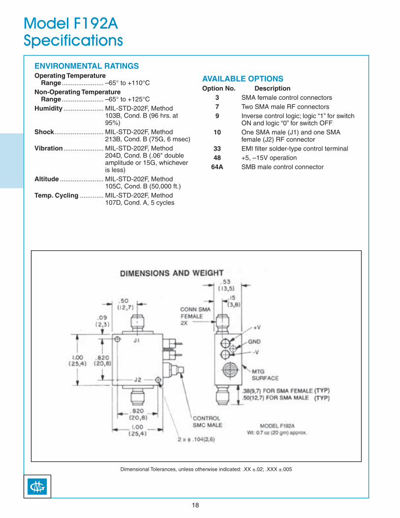
Model F192ASpecifications
PERFORMANCE CHARACTERISTICS
Switching Speed Rise Time ............... 10 nsec. max. Fall Time ................. 10 nsec. max. ON Time ................. 30 nsec. max. OFF Time ............... 15 nsec. max.Power Handling Capability Without Performance
Degradation ........ 500 mW cw or peak Survival Power ....... 1W average, 10W peak
(1 µsec max. pulse width)Power Supply Requirements +5V ±5%, 90 mA
–12V ±5%, 75 mA
Control Characteristics Control Input Impedance .......... TTL, advanced Schottky,
one-unit load. (A unit load is 0.6 mA sink current and 20 µA source current.)
Control Logic .......... Logic “0” (–0.3 to +0.8V) for switch ON and logic “1” (+2.0 to +5.0V) for switch OFF.
CHARACTERISTIC
FREQUENCY (GHz)0.2 to 0.5
0.5 to 2.0
2.0 to 8.0
8.0 to
12.4
12.4 to
18.0
Min Isolation (dB) Max Insertion Loss (dB) VSWR (ON and OFF)
70 2.0 1.5
80 2.0 1.5
80 2.5 1.75
80 3.0 2.0
80 3.5 2.0
18
Model F192ASpecifications
Dimensional Tolerances, unless otherwise indicated: .XX ±.02; .XXX ±.005
ENVIRONMENTAL RATINGSOperating Temperature Range ....................... –65° to +110°CNon-Operating Temperature Range ....................... –65° to +125°CHumidity ...................... MIL-STD-202F, Method
103B, Cond. B (96 hrs. at 95%)
Shock ........................... MIL-STD-202F, Method 213B, Cond. B (75G, 6 msec)
Vibration ...................... MIL-STD-202F, Method 204D, Cond. B (.06" double amplitude or 15G, whichever is less)
Altitude ........................ MIL-STD-202F, Method 105C, Cond. B (50,000 ft.)
Temp. Cycling ............. MIL-STD-202F, Method 107D, Cond. A, 5 cycles
AVAILABLE OPTIONS Option No. Description 3 SMA female control connectors 7 Two SMA male RF connectors 9 Inverse control logic; logic “1” for switch
ON and logic “0” for switch OFF 10 One SMA male (J1) and one SMA
female (J2) RF connector 33 EMI filter solder-type control terminal 48 +5, –15V operation 64A SMB male control connector

19
Series 195 Octave-BandPIN Diode Attenuator/Modulators
SERIES 195Series 195 current-controlled attenuator/modulators provide small size with greater than octave-bandwidth performance at low cost. All models except the 1950A* provide a minimum of 60 dB of attenuation with fall times of 20 nsec max, and rise times ranging from 25 nsec for the 1951 and 1952 to 125 nsec max for the 1956 and 1958. The 1950A* provides a minimum of 80 dB of attenuation with a fall time of 50 nsec max and a rise time of 250 nsec max.These characteristics make this series suitable for a wide range of applications including level setting, complex amplitude modulation, pulse modulation and high-speed switching.The eight models in the Series 195 encompass a frequency range from 0.5 to 18 GHz. All models except the 1950A* are capable of extended bandwidth operation, typically 3:1, with only moderate degradation in performance at the band edges.As shown in figures 1 and 2 below, the RF circuit employed in all models except the Model 1950A* uses two shunt arrays of PIN diodes and two quadrature hybrid couplers. The quadrature hybrids are of a unique GMC microstrip design which are integrated with the diode arrays to yield a minimal package size. The RF circuit employed in the Model 1950A* uses one shunt array of PIN diodes with input and output impedance matching circuits.
Fig. 1–Models 1951-1958, rf schematic diagram.
Fig. 2–Model 1950A*, RF schematic diagram.
* Model 1950A is a special-order product. Consult factory before ordering.
• Absorptive• Current controlled• 0.5 to 18 GHz frequency range• High performance MIC
quadrature hybrid design• High speed
20
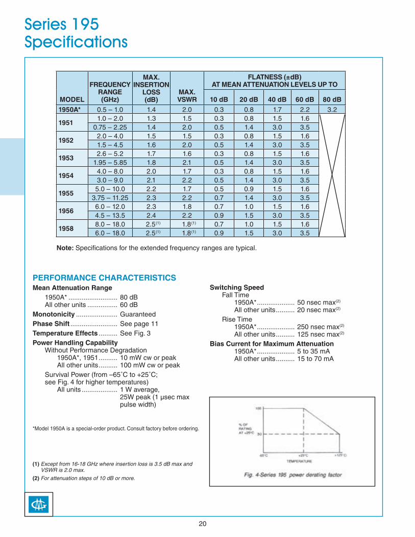
Series 195Specifications
PERFORMANCE CHARACTERISTICSMean Attenuation Range 1950A* .......................... 80 dB All other units ................ 60 dBMonotonicity ...................... GuaranteedPhase Shift ......................... See page 11Temperature Effects .......... See Fig. 3Power Handling Capability Without Performance Degradation 1950A*, 1951 .......... 10 mW cw or peak All other units .......... 100 mW cw or peak Survival Power (from –65˚C to +25˚C; see Fig. 4 for higher temperatures) All units ................... 1 W average,
25W peak (1 µsec max pulse width)
Switching Speed Fall Time 1950A* .................... 50 nsec max(2)
All other units .......... 20 nsec max(2)
Rise Time 1950A* .................... 250 nsec max(2)
All other units .......... 125 nsec max(2)
Bias Current for Maximum Attenuation 1950A* .................... 5 to 35 mA All other units .......... 15 to 70 mA
*Model 1950A is a special-order product. Consult factory before ordering.
(1) Except from 16-18 GHz where insertion loss is 3.5 dB max and VSWR is 2.0 max.
(2) For attenuation steps of 10 dB or more.
Note: Specifications for the extended frequency ranges are typical.
MODEL
FREQUENCY RANGE (GHz)
MAX. INSERTION
LOSS (dB)
MAX. VSWR
FLATNESS (±dB) AT MEAN ATTENUATION LEVELS UP TO
10 dB 20 dB 40 dB 60 dB 80 dB1950A* 0.5 – 1.0 1.4 2.0 0.3 0.8 1.7 2.2 3.2
19511.0 – 2.0 1.3 1.5 0.3 0.8 1.5 1.6
0.75 – 2.25 1.4 2.0 0.5 1.4 3.0 3.5
19522.0 – 4.0 1.5 1.5 0.3 0.8 1.5 1.61.5 – 4.5 1.6 2.0 0.5 1.4 3.0 3.5
19532.6 – 5.2 1.7 1.6 0.3 0.8 1.5 1.6
1.95 – 5.85 1.8 2.1 0.5 1.4 3.0 3.5
19544.0 – 8.0 2.0 1.7 0.3 0.8 1.5 1.63.0 – 9.0 2.1 2.2 0.5 1.4 3.0 3.5
19555.0 – 10.0 2.2 1.7 0.5 0.9 1.5 1.6
3.75 – 11.25 2.3 2.2 0.7 1.4 3.0 3.5
19566.0 – 12.0 2.3 1.8 0.7 1.0 1.5 1.64.5 – 13.5 2.4 2.2 0.9 1.5 3.0 3.5
19588.0 – 18.0 2.5(1) 1.8(1) 0.7 1.0 1.5 1.66.0 – 18.0 2.5(1) 1.8(1) 0.9 1.5 3.0 3.5
21
Series 195Specifications
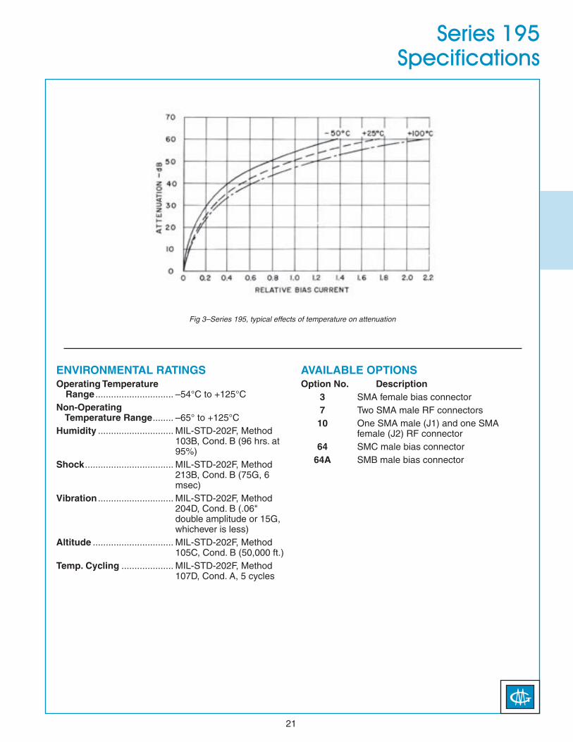
Fig 3–Series 195, typical effects of temperature on attenuation
ENVIRONMENTAL RATINGSOperating Temperature Range .............................. –54°C to +125°CNon-Operating Temperature Range ........ –65° to +125°CHumidity ............................. MIL-STD-202F, Method
103B, Cond. B (96 hrs. at 95%)
Shock .................................. MIL-STD-202F, Method 213B, Cond. B (75G, 6 msec)
Vibration ............................. MIL-STD-202F, Method 204D, Cond. B (.06" double amplitude or 15G, whichever is less)
Altitude ............................... MIL-STD-202F, Method 105C, Cond. B (50,000 ft.)
Temp. Cycling .................... MIL-STD-202F, Method 107D, Cond. A, 5 cycles
AVAILABLE OPTIONS Option No. Description 3 SMA female bias connector 7 Two SMA male RF connectors 10 One SMA male (J1) and one SMA
female (J2) RF connector 64 SMC male bias connector 64A SMB male bias connector
22
Series 195Specifications
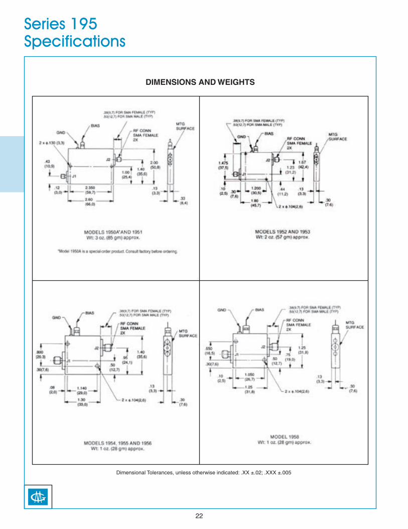
DIMENSIONS AND WEIGHTS
Dimensional Tolerances, unless otherwise indicated: .XX ±.02; .XXX ±.005

Series D195 Octave-BandPIN Diode Attenuator/Modulators
With Integrated Drivers
SERIES D195The Series D195 voltage-controlled linearized attenuator/modulators are integrated assemblies consisting of a Series 195 unit and a hybridized driver circuit which provides a nominal transfer function of 10 dB per volt. (See figure 1 below.)
All of the Series D195 units except the D1950A* exhibit fall times of 20 nsec max and rise times of 1.5 µsec max for attenuation steps of 10 dB or more. For smaller excursions, the fall times can increase to several hundred nsec, while the rise times remain essentially unchanged. In applications where a rapid return to insertion loss from any level of attenuation is required, Option 59 is available. With this option, an external pulse is applied to trigger a high-speed reset circuit, and recovery times of 200 nsec max are obtained. Where use of an external reset pulse as described above is not feasible, an internal reset option (Option 58) is available which will automatically reset the unit to insertion loss within 200 nsec for a step of 50 dB or more.The fall and rise time specifications for the D1950A* are 500 nsec max and 10 µsec max, respectively. Options 58 and 59 are not available for this model.
* Model D1950A is a special-order product. Consult factory before ordering.
ALL UNITS IN THIS SERIES ARE EQUIPPED WITH INTEGRATED DRIVERS
• Absorptive• Linearized• Frequency range: 0.5 to 18 GHz• High performance MIC quadrature
hybrid design• High speed
23

24
Series D195Specifications
PERFORMANCE CHARACTERISTICSMean Attenuation Range D1950A* ............................80 dB All other units ....................60 dBAccuracy of Attenuation 0-30 dB .............................±0.5 dB >30 to 50 dB ......................±1.0 dB >50 to 60 dB ......................±1.5 dB >60 to 80 dB ...................... ±2.0 dB
(D1950A* only)Monotonicity ..........................GuaranteedPhase Shift .............................See page 11Temperature Coefficient .......±0.025 dB/°CPower Handling Capability Without Performance Degradation D1950A*, D1951 ...........10 mW cw or peak All other units ................. 100 mW cw or peak
Survival Power (from –65°C to +25°C; see figure 2 for higher temperatures)
All Units ......................... 1W average 25W peak (1 µsec max pulse width)
Switching Characteristics OFF Time D1950A* ........................600 nsec max All other units .................100 nsec max
* Model 1950A is a special-order product. Consult factory before ordering.
(1) Except from 16-18 Ghz where insertion loss is 4.0 dB max and VSWR is 2.0 max.
ON Time D1950A* ........................10 µsec max All other units .................1.6 µsec max Fall Time D1950A* ........................500 nsec max All other units .................20 nsec max Rise Time D1950A* ........................10 µsec max All other units .................1.5 µsec maxNominal Control Voltage Characteristics Range Operating Maximum D1950A* 0 to +8V ±15V All other units 0 to +6V ±15V Transfer Function ............10 dB/volt Input Impedance .............10 Kohms Modulation Bandwidth Small Signal D1950A* ....................25 kHz All other units .............500 kHz Large Signal D1950A* ....................5 kHz All other units .............50 kHz
Power Supply Requirements .................. +12V ±5%, 100 mA
–12V ±5%, 50 mAPower Supply Rejection .......................... Less than 0.1 dB/volt
change in either supply
MODEL
FREQUENCY RANGE (GHz)
MAX. INSERTION
LOSS (dB)
MAX. VSWR
FLATNESS (±dB) AT MEAN ATTENUATION LEVELS UP TO
10 dB 20 dB 40 dB 60 dB 80 dB
D1950A* 0.5 – 1.0 1.4 2.0 0.3 0.8 1.7 3.0 3.6
D19511.0 – 2.0 1.6 1.5 0.3 0.8 1.5 1.6
0.75 – 2.25 1.7 2.0 0.5 1.4 3.0 3.5
D19522.0 – 4.0 1.8 1.5 0.3 0.8 1.5 1.61.5 – 4.5 1.9 2.0 0.5 1.4 3.0 3.5
D19532.6 – 5.2 2.0 1.6 0.3 0.8 1.5 1.6
1.95 – 5.85 2.1 2.1 0.5 1.4 3.0 3.5
D19544.0 – 8.0 2.4 1.7 0.3 0.8 1.5 1.63.0 – 9.0 2.5 2.2 0.5 1.4 3.0 3.5
D19555.0 – 10.0 2.6 1.7 0.5 0.9 1.5 1.6
3.75 – 11.25 2.7 2.2 0.7 1.4 3.0 3.5
D19566.0 – 12.0 2.7 1.8 0.7 1.0 1.5 1.64.5 – 13.5 2.8 2.2 0.9 1.5 3.0 3.5
D19588.0 – 18.0 3.0(1) 1.8(1) 0.7 1.0 1.5 1.66.0 – 18.0 3.0(1) 1.8(1) 0.9 1.5 3.0 3.5
Note: Specifications for the extended frequency ranges are typical.

25
Series D195Specifications
(1) Where use of an Option 59 external reset pulse (see note 2 below) is not feasible, this option is available which will automatically sense the slope and magnitude of the control signal and reset the unit to the insertion loss state within 200 nsec for a step of 50 dB or more.
(2) An external terminal is provided for the user to apply a fast (10 nsec max rise time) positive-going 3-volt pulse at least 0.5 µsec wide to accelerate the return of the attenuator to the insertion loss state with the simultaneous lowering of the control signal to the zero voltage level. This reset can be accomplished within 200 nsec.
(3) The input impedance of units equipped with Option 59 is a circuit equivalent to approximately 50 pF in series with a parallel combination of 100 pF and 1000 ohms.
*Model D1950A is a special-order product. Consult factory befor ordering.
ENVIRONMENTAL RATINGSOperating Temperature Range ....................... –54° to +110°CNon-Operating Temperature Range ....................... –65° to +125°CHumidity ......................... MIL-STD-202F, Method
103B, Cond. B (96 hrs. at 95%)
Shock .............................. MIL-STD-202F, Method 213B, Cond. B (75G, 6 msec)
Vibration ......................... MIL-STD-202F, Method 204D, Cond. B (.06" double amplitude or 15G, whichever is less)
Altitude ........................... MIL-STD-202F, Method 105C, Cond. B (50,000 ft.)
Temp. Cycling ................ MIL-STD-202F, Method 107D, Cond. A, 5 cycles
AVAILABLE OPTIONS Option No. Description 3 SMA female control connector 7 Two SMA male RF connectors 10 One SMA male (J1) and one SMA
female (J2) RF connector 58 Internally-generated reset to insertion
loss (not available on D1950A)(1)
59 Externally-triggered reset to insertion loss (not available on D1950A)(2) (3)
61 20 dB/volt transfer function with 0 to +3V control signal input (+4V for the D1950A*)
62 ±15 volt operation 64 SMC male control connector 64A SMB male control connector

26
Series D195Specifications
DIMENSIONS AND WEIGHTS
Dimensional Tolerances, unless otherwise indicated: .XX ±.02; .XXX ±.005
MODEL DIM “A”
D1950A D1951
.70 (17,8)
.50 (12,7)

27
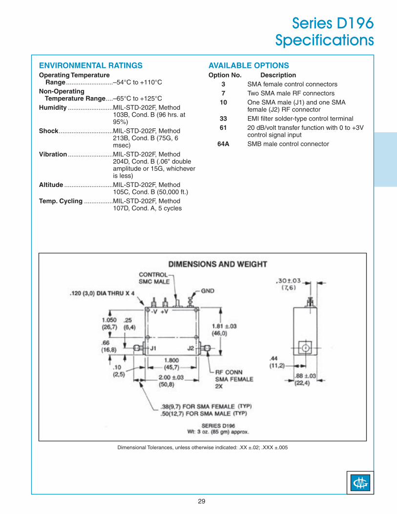
D196 Series Multi-OctavePIN Diode Attenuators
With Integrated Drivers (0.5-18 GHz)
The D196 Series is a family of nonreflective voltage variable 60 dB PIN Diode Attenuators covering the frequency range from 0.5 GHz to 18 GHz in four overlapping multi-octave bands.Each model in the Series is equipped with an integrated driver which controls the attenuation level at the rate of 10 dB/volt.The RF circuit consists of two wide-band, T-pad attenuator sections connected in tandem. The driver circuit, which consists of a voltage-to-current converter and linearizing network, furnishes the proper series and shunt currents to control the attenuation value at the specified rate while simultaneously maintaining a bilateral match. See figs. 1 and 2.
All units in this series are equipped with integrated drivers
• Frequency range: 0.5 GHz-18 GHz in four overlapping bands
• Attenuation range: 60 dB• Linear control: 10 dB/volt• Low insertion loss• Nonreflective
28
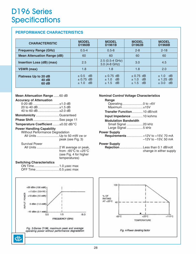
PERFORMANCE CHARACTERISTICS
D196 Series Specifications
Mean Attenuation Range ......60 dBAccuracy of Attenuation 0-20 dB .............................±1.0 dB 20 to 40 dB ........................±1.5 dB 40 to 60 dB ........................ ±2.0 dBMonotonicity ..........................GuaranteedPhase Shift .............................See page 11Temperature Coefficient .......±0.02 dB/°CPower Handling Capability Without Performance Degradation All Units ......................... Up to 50 mW cw or
peak (see Fig. 3) Survival Power All Units ......................... 2 W average or peak,
from –65°C to +25°C (see Fig. 4 for higher temperatures)
Switching Characteristics ON Time ............................1.0 µsec max OFF Time ..........................0.5 µsec max
Nominal Control Voltage Characteristics Range Operating .......................0 to +6V Maximum .......................±15V Transfer Function ............10 dB/volt Input Impedance .............10 kohms Modulation Bandwidth Small Signal ..................20 kHz Large Signal ..................5 kHzPower Supply Requirements .................. +12V to +15V, 70 mA
–12V to –15V, 50 mAPower Supply Rejection .......................... Less than 0.1 dB/volt
change in either supply
CHARACTERISTIC MODEL D1960B
MODEL D1961B
MODEL D1962B
MODEL D1968B
Frequency Range (GHz) 0.5-4 0.5-8 2-8 2-18
Mean Attenuation Range (dB) 60 60 60 60
Insertion Loss (dB) (max) 2.5 2.5 (0.5-4 GHz) 3.0 (4-8 GHz) 3.0 4.5
VSWR (max) 1.8 1.8 1.8 2.0
Flatness Up to 20 dB 40 dB 60 dB
± 0.5 dB ± 0.75 dB ± 1.0 dB
± 0.75 dB ± 1.0 dB ± 1.5 dB
± 0.75 dB ± 1.0 dB ± 1.5 dB
± 1.0 dB ± 1.25 dB ± 3.0 dB
29
Series D196Specifications
ENVIRONMENTAL RATINGSOperating Temperature Range .......................... –54°C to +110°CNon-Operating Temperature Range .... –65°C to +125°CHumidity ......................... MIL-STD-202F, Method
103B, Cond. B (96 hrs. at 95%)
Shock .............................. MIL-STD-202F, Method 213B, Cond. B (75G, 6 msec)
Vibration ......................... MIL-STD-202F, Method 204D, Cond. B (.06" double amplitude or 15G, whichever is less)
Altitude ........................... MIL-STD-202F, Method 105C, Cond. B (50,000 ft.)
Temp. Cycling ................ MIL-STD-202F, Method 107D, Cond. A, 5 cycles
AVAILABLE OPTIONS Option No. Description 3 SMA female control connectors 7 Two SMA male RF connectors 10 One SMA male (J1) and one SMA
female (J2) RF connector 33 EMI filter solder-type control terminal 61 20 dB/volt transfer function with 0 to +3V
control signal input 64A SMB male control connector
Dimensional Tolerances, unless otherwise indicated: .XX ±.02; .XXX ±.005
30
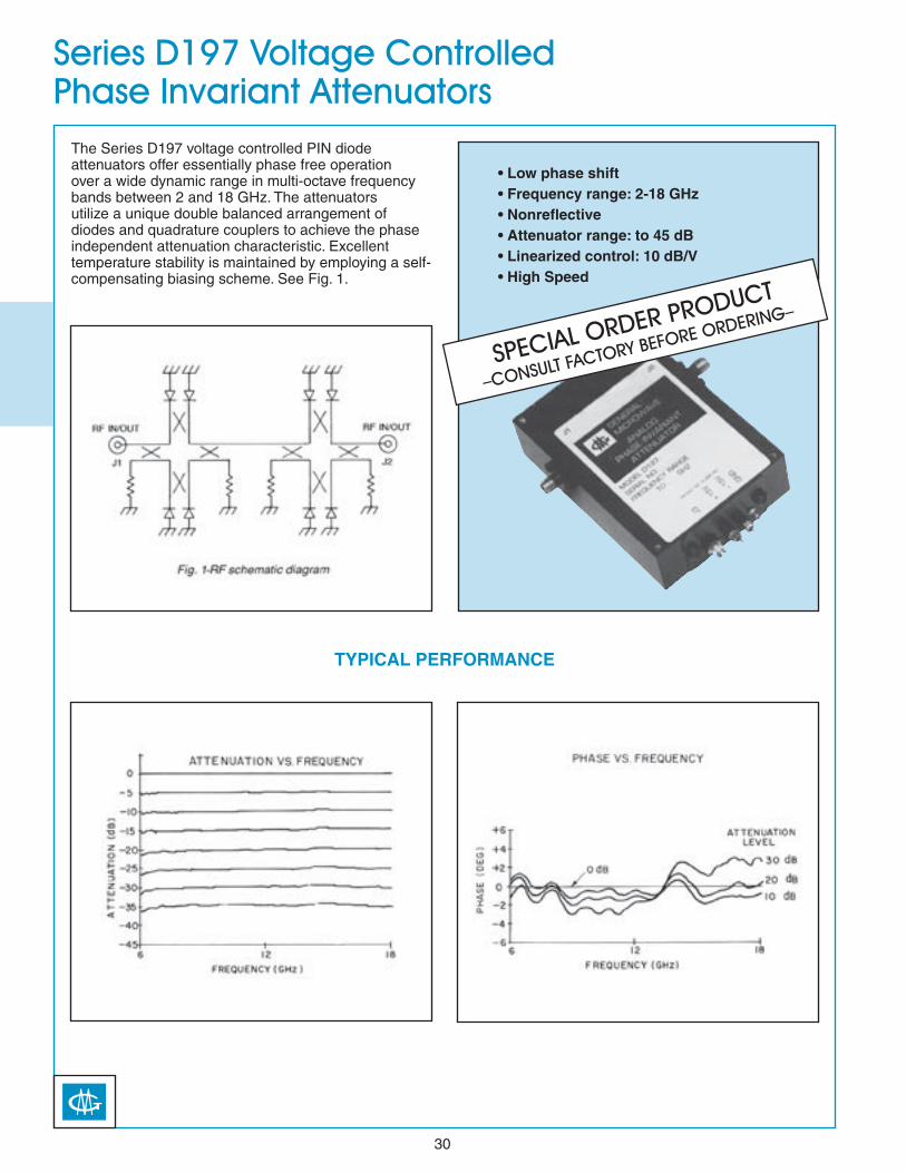
Series D197 Voltage ControlledPhase Invariant Attenuators
The Series D197 voltage controlled PIN diode attenuators offer essentially phase free operation over a wide dynamic range in multi-octave frequency bands between 2 and 18 GHz. The attenuators utilize a unique double balanced arrangement of diodes and quadrature couplers to achieve the phase independent attenuation characteristic. Excellent temperature stability is maintained by employing a self-compensating biasing scheme. See Fig. 1.
• Low phase shift• Frequency range: 2-18 GHz• Nonreflective• Attenuator range: to 45 dB• Linearized control: 10 dB/V• High Speed
TYPICAL PERFORMANCE
SPECIAL ORDER PRODUCT
–CONSULT FACTORY BEFORE ORDERING–

31
Series D197Specifications
(1) Except from 8-18 GHz, flatness is ±0.5 dB up to 20 dB, ±1.0 dB up to 32 dB.
SPECIFICATIONS WITH EXTENDED RANGE OPTION (OPTION 45)
PERFORMANCE CHARACTERISTICSMODEL D1972 D1974 D1978
Frequency Range (GHz) 2-6 4-11 6-18
Mean Attenuation Range 32 dB
Insertion Loss (Max) 4 dB 5 dB 5.5 dB
VSWR (Max) 2.0
Accuracy of Attenuation 0 to 20 dB > 20 to 32 dB
± 1.0 dB ± 2.0 dB
Amplitude Flatness 0 to 20 dB > 20 to 32 dB
± 0.4 dB ± 0.6 dB
± 0.4 dB ± 0.8 dB
± 0.8 dB(1) ± 1.3 dB(1)
Monotonicity Guaranteed
Phase Shift 0 to 20 dB > 20 to 32 dB
± 4° ± 8°
± 4° ± 8°
± 5° ± 10°
Control Voltage 0-3.2 V
Control Input Impedance 10 kohms
Transfer Function 10 dB/V
On Time, Off Time 250 nsec
Temperature Coefficient 0 - 20 dB > 20 - 32 dB
.01 dB/°C
.03 dB/°C
Max. RF Power Input (Operating) 100 mW
Max. RF Power Input (Survival) 0.5 W
Harmonic Distortion @ Pin = +10 dBm – 40 dBc – 50 dBc – 50 dBc
Power Supply Requirements+15V ± 5% @ 200 mA – 15V ± 5% @ 120 mA
Mean Attenuation Range 45 dB
Accuracy of Attenuation 0-20 dB > 20-32 dB > 32 dB
± 1.0 dB ± 2.0 dB ± 3.5 dB
Amplitude Flatness 0 to 20 dB > 20 to 32 dB > 32 dB
± 0.4 dB ± 0.6 dB ± 1.5 dB
± 0.4 dB ± 0.8 dB ± 1.5 dB
± 0.8 dB(1)
± 1.3 dB(1)
± 2.0 dB
Phase Variation 0 to 20 dB > 20 to 32 dB > 32 dB
± 4° ± 8° ± 15°
± 4° ± 8° ± 20°
± 5° ± 10° ± 30°

32
Series D197Specifications
ENVIRONMENTAL RATINGSOperating Temperature Range .............................. –54° to +110°CNon-Operating Temperature Range ........ –65° to +125°CHumidity ............................. MIL-STD-202F, Method
103B, Cond. B (96 hrs. at 95%)
Shock .................................. MIL-STD-202F, Method 213B, Cond. B (75G, 6 msec)
Vibration ............................. MIL-STD-202F, Method 204D, Cond. B (.06" double amplitude or 15G, whichever is less)
Altitude ............................... MIL-STD-202F, Method 105C, Cond. B (50,000 ft.)
Temp. Cycling .................... MIL-STD-202F, Method 107D, Cond. A, 5 cycles
AVAILABLE OPTIONS Option No. Description 7 Two SMA male RF connectors 10 One SMA male (J1) and one SMA
female (J2) RF connector 45 Extended attenuation range to 45 dB 65 ±12V operation
Dimensional Tolerances, unless otherwise indicated: .XX ±.02; .XXX ±.005
MODEL A B C D E F G H
D1972 2.5 (63,5) 2.26 (57,4) 2.28 (57,9) 0.22 (5,6) 0.91 (23,1) 1.25 (31,7) 1.5 (38,1) 1.7 (43,2)
D1974 2.0 (50,8) 1.76 (44,7) 2.43 (61,7) 0.18 (4,6) 0.66 (16,8) 1.0 (25,4) 1.25 (31,7) 1.45 (36,8)
D1978 2.0 (50,8) 1.76 (44,7) 2.58 (65,5) 0.18 (4,6) 0.66 (16,8) 1.0 (25,4) 1.25 (31,7) 1.50 (38,1)

33
Model 3250A Ultra-Broadband6 Bit Digital PIN Diode Attenuator
• Frequency range: 0.2 to 18 GHz• Attenuation range: Up to 60 dB• 6 Bit Binary or BCD programming• Absorptive• Guaranteed Monotonicity
The Model 3250A digitally programmable attenuator provides excellent performance characteristics over the frequency range of 0.2 to 18 GHz. Attenuation levels up to 60 dB are programmable in increments of 1 dB.The unit is an integrated assembly of a dual T-pad PIN diode attenuator and a driver consisting of a D/A and an I/V Converter. See figures 1 and 2.The Model 3250A operates as a bilaterally-matched device at all attenuation levels. It is supplied in a compact rugged package well-suited to military applications.
34
Model 3250ASpecifications
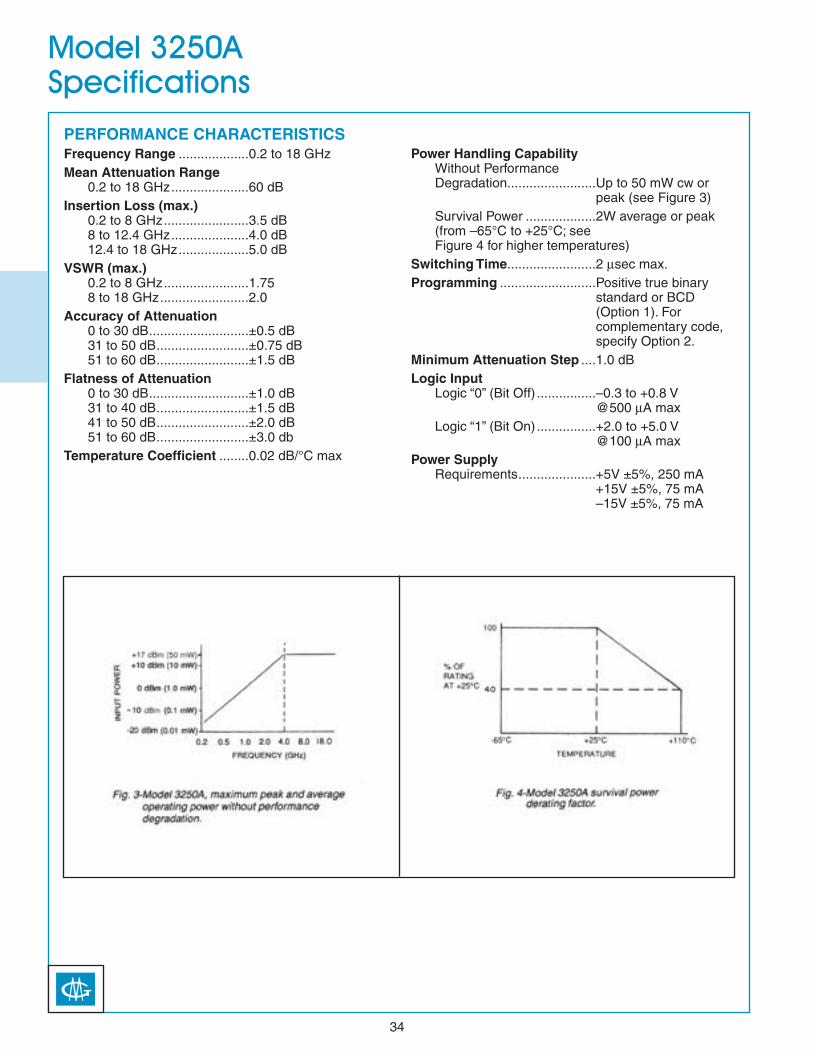
PERFORMANCE CHARACTERISTICSFrequency Range ...................0.2 to 18 GHzMean Attenuation Range 0.2 to 18 GHz .....................60 dBInsertion Loss (max.) 0.2 to 8 GHz .......................3.5 dB 8 to 12.4 GHz .....................4.0 dB 12.4 to 18 GHz ...................5.0 dBVSWR (max.) 0.2 to 8 GHz .......................1.75 8 to 18 GHz ........................2.0Accuracy of Attenuation 0 to 30 dB ...........................±0.5 dB 31 to 50 dB .........................±0.75 dB 51 to 60 dB .........................±1.5 dBFlatness of Attenuation 0 to 30 dB ...........................±1.0 dB 31 to 40 dB .........................±1.5 dB 41 to 50 dB .........................±2.0 dB 51 to 60 dB .........................±3.0 dbTemperature Coefficient ........0.02 dB/°C max
Power Handling Capability Without Performance Degradation ........................ Up to 50 mW cw or
peak (see Figure 3) Survival Power ................... 2W average or peak (from –65°C to +25°C; see
Figure 4 for higher temperatures)Switching Time ........................2 µsec max.Programming .......................... Positive true binary
standard or BCD (Option 1). For complementary code, specify Option 2.
Minimum Attenuation Step ....1.0 dBLogic Input Logic “0” (Bit Off) ................ –0.3 to +0.8 V
@500 µA max Logic “1” (Bit On) ................ +2.0 to +5.0 V
@100 µA maxPower Supply Requirements ..................... +5V ±5%, 250 mA
+15V ±5%, 75 mA –15V ±5%, 75 mA
35
Model 3250ASpecifications
Dimensional Tolerances, unless otherwise indicated: .XX ±.02; .XXX ±.005
ENVIRONMENTAL RATINGSOperating Temperature Range ........................ –54°C to +110°CNon-Operating Temperature Range ........................ –65°C to +125°CHumidity ....................... MIL-STD-202F, Method 103B,
Cond. B (96 hrs. at 95%)Shock ............................ MIL-STD-202F, Method 213B,
Cond. B (75G, 6 msec)Vibration ....................... MIL-STD-202F, Method
204D, Cond. B (.06" double amplitude or 15G, whichever is less)
Altitude ......................... MIL-STD-202F, Method 105C, Cond. B (50,000 ft.)
Temp. Cycling .............. MIL-STD-202F, Method 107D, Cond. A, 5 cycles
AVAILABLE OPTIONS Option No. Description 1 BDC programming
(Binary is standard) 2 Complementary programming
(positive true is standard) 7 Two SMA male RF connectors 10 One SMA male (J1) and one SMA
female (J2) RF connector 5002* 8-Bit Resolution, 1 µsec switching time
ACCESSORY FURNISHEDMating power/logic connector
* Special order product. Consult factory before ordering. In addition, consult factory for impact on specifications; i.e., VSWR and insertion loss and availability.
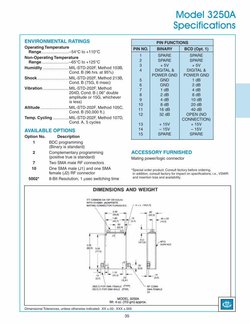
PIN FUNCTIONS
PIN NO. BINARY BCD (Opt. 1)
1 2 3 4 5 6 7 8 9 10 11 12
13 14 15
SPARE SPARE
+ 5V DIGITAL &
POWER GND GND GND 1 dB 2 dB 4 dB 8 dB 16 dB 32 dB
+ 15V – 15V
SPARE
SPARE SPARE
+ 5V DIGITAL &
POWER GND 1 dB 2 dB 4 dB 8 dB 10 dB 20 dB 40 dB
OPEN (NO CONNECTION)
+ 15V – 15V
SPARE
36
346C Series Multi-Octave10 Bit Digital PIN Diode Attenuators(0.5-18 GHz)
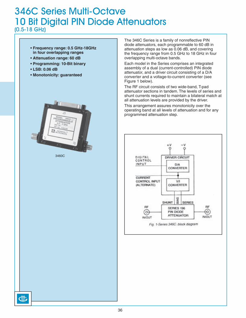
The 346C Series is a family of nonreflective PIN diode attenuators, each programmable to 60 dB in attenuation steps as low as 0.06 dB, and covering the frequency range from 0.5 GHz to 18 GHz in four overlapping multi-octave bands.Each model in the Series comprises an integrated assembly of a dual (current-controlled) PIN diode attenuator, and a driver circuit consisting of a D/A converter and a voltage-to-current converter (see Figure 1 below).The RF circuit consists of two wide-band, T-pad attenuator sections in tandem. The levels of series and shunt currents required to maintain a bilateral match at all attenuation levels are provided by the driver.This arrangement assures monotonicity over the operating band at all levels of attenuation and for any programmed attenuation step.
• Frequency range: 0.5 GHz-18GHz in four overlapping ranges
• Attenuation range: 60 dB • Programming: 10-Bit binary • LSB: 0.06 dB • Monotonicity: guaranteed
3460C

37
Series 346CSpecifications
PERFORMANCE CHARACTERISTICS
Accuracy of Attenuation 0-20 dB .............................±1.0 dB 20-40 dB ...........................±1.5 dB 40-60 dB ...........................±2.0 dBMonotonicity ..........................GuaranteedPhase Shift .............................See figure 2Temperature Coefficient .......±0.02 dB/°CPower Handling Capability Without Performance Degradation All Units ......................... Up to 50 mW cw or
peak (see figure 3) Survival Power All Units ......................... 2 W average or peak,
from –65°C to +25°C (see figure 4 for higher temperatures)
Switching Time ON Time ............................1.0 µsec. max. OFF Time ..........................0.5 µsec. max.Programming ......................... Positive true binary.
For complementary code, specify Option 2. To interface with other logic families, please contact factory.
Minimum Attenuation Step ...0.06 dB(1)
Logic Input Logic “0” (Bit OFF) ............–0.3 to +0.8 V Logic “1” (Bit ON) ..............+2.0 to +5.0 V Input Current .....................10 µA max.Nominal Control Voltage Characteristics Range ...............................0 to 2 mA Transfer Function ............30 dB/mA Input Impedance .............3 kohmsPower Supply Requirements .................. +12V to +15V, 80 mA
–12V to –15V, 60 mAPower Supply Rejection .......................... Less than 0.1 dB/volt
change in either supply
CHARACTERISTIC MODEL 3460C
MODEL 3461C
MODEL 3462C
MODEL 3468C
Frequency Range (GHz) 0.5-4 0.5-8 2-8 2-18Mean Attenuation Range (dB) 60 60 60 60
Insertion Loss (dB) (max) 2.5 2.5 (0.5-4 GHz) 3.0 (4-8 GHz) 3.0 4.5
VSWR (max) 1.8 1.8 1.8 2.0Flatness up to 20 dB 40 dB 60 dB
± 0.5 dB ± 0.75 dB ± 1.0 dB
± 0.75 dB ± 1.0 dB ± 1.5 dB
± 0.75 dB ± 1.0 dB ± 1.5 dB
± 1.0 dB ± 1.25 dB ± 3.0 dB
(1) See note (4) on page 38
38
Series 346CSpecifications
ENVIRONMENTAL RATINGSOperating Temperature Range .............................. –54°C to +110°CNon-Operating Temperature Range ........ –65°C to +125°CHumidity ............................. MIL-STD-202F, Method
103B, Cond. B (96 hrs. at 95%)
Shock .................................. MIL-STD-202F, Method 213B, Cond. B (75G, 6 msec)
Vibration ............................. MIL-STD-202F, Method 204D, Cond. B (.06" double amplitude or 15G, whichever is less)
Altitude ............................... MIL-STD-202F, Method 105C, Cond. B (50,000 ft.)
Temp. Cycling .................... MIL-STD-202F, Method 107D, Cond. A, 5 cycles
AVAILABLE OPTIONS Option No. Description 2 Complementary programming
(logic “0” is bit on) 7 Two SMA male RF connectors 10 One SMA male (J1) and one SMA
female (J2) RF connector
ACCESSORY FURNISHEDMating power/logic connector
(1) All unused inputs must be grounded.(2) For normal programming control Pin 1 must be grounded
or at logic “0”. Application of logic “1” to Pin 1 overrides the digital input and sets the unit to insertion loss. For units with complementary programming (Option 2), the application of a logic “1” to Pin 1 sets the unit to high isolation (60 dB or greater).
(3) Pin 2 is available to (a) monitor the D/A converter output, (b) apply a modulation signal from a current source, or (c) apply an independent analog signal for turn-on, turn-off or vernier attenuation levels. If not used as described in (a), (b) or (c), Pin 2 must be open.
(4) The Series 346C attenuators are 10-bit digital attenuators. In order to use this device with a lesser number of bits (lower resolution), the user may simply ground the logic pins for the lowest order unused bits. For example, a Series 346C unit operated as an 8-bit unit would have Pin 15 and Pin 3 connected to ground. All other parameters remain unchanged.
Dimensional Tolerances, unless otherwise indicated: .XX ±.02; .XXX ±.005
PIN J3 PIN FUNCTIONS(1) (4)
1 2 3 4 5 6 7 8 9 10 11 12 13 14 15
GND (Note 2) ANOLOG INPUT (Note 3) 0.13 dB GND 0.25 dB 0.5 dB 1 dB 2 dB 4 dB 8 dB 16 dB 32 dB (MSB) +V –V 0.06 dB (LSB)

39
Series 347, 8 Bit DigitalPhase Invariant Attenuators
The Series 347 digitally controlled PIN diode attenuators offer essentially phase free operation over a wide dynamic range in multi-octave frequency bands between 2 and 18 GHz. The attenuators utilize a unique double balanced arrangement of diodes and quadrature couplers to achieve the phase independent attenuation characteristic. Excellent temperature stability is maintained by employing a self-compensating biasing scheme. See Fig. 1.
TYPICAL PERFORMANCE
SPECIAL ORDER PRODUCT
–CONSULT FACTORY BEFORE ORDERING–

40
Series 347Specifications
(1) Except from 8-18 GHz, flatness is ±0.5 dB up to 20 dB, ±1.0 dB up to 32 dB.
SPECIFICATIONS WITH EXTENDED RANGE OPTION (OPTION 45)
PERFORMANCE CHARACTERISTICSMODEL 3472 3474 3478
Frequency Range (GHz) 2-6 4-11 6-18
Mean Attenuation Range 32 dB
Insertion Loss (Max) 4 dB 5 dB 5.5 dB
VSWR (Max) 2.0
Accuracy of Attenuation ± 0.5 dB
Amplitude Flatness 0 to 20 dB > 20 to 32 dB
± 0.4 dB ± 0.6 dB
± 0.4 dB ± 0.8 dB
± 0.8 dB(1) ± 1.3 dB(1)
Monotonicity Guaranteed
Phase Shift 0 to 20 dB > 20 to 32 dB
± 4° ± 8°
± 4° ± 8°
± 5° ± 10°
ON Time, OFF Time 350 nsec
Temperature Coefficient .02 dB/°C
Max. RF Power Input (Operating) 100 mW
Max. RF Power Input (Survival) 0.5 W
Harmonic Distortion @ Pin = +10 dBm – 40 dBc – 50 dBc – 50 dBc
Control 8 bit TTL, 0.125 dB LSB
Control Input Impedance@ Logic “0” (–0.3 to +0.8 V), 500 µA max.@ Logic “1” (+2.0 to +5.0 V), 100 µA max.
Logic Input Logic “0” = Bit OFF; Logic “1” = Bit ON
Power Supply Requirements +5V ± 5% @ 325 mA+15V ± 5% @ 15 mA –15V ± 5% @ 70 mA
Mean Attenuation Range 45 dB
Accuracy of Attenuation ± 1.0 dB
Amplitude Flatness 0 to 20 dB > 20 to 32 dB > 32 dB
± 0.4 dB ± 0.6 dB ± 1.5 dB
± 0.4 dB ± 0.8 dB ± 1.5 dB
± 0.8 dB(1)
± 1.3 dB(1)
± 2.0 dB
Phase Variation 0 to 20 dB > 20 to 32 dB > 32 dB
± 4° ± 8° ± 15°
± 4° ± 8° ± 20°
± 5° ± 10° ± 30°
Control 8 bit TTL, 0.176 dB LSB

41
Series 347Specifications
ENVIRONMENTAL RATINGSOperating Temperature Range .............................. –54°C to +110°CNon-Operating Temperature Range ........ –65°C to +125°CHumidity ............................. MIL-STD-202F, Method
103B, Cond. B (96 hrs. at 95%)
Shock .................................. MIL-STD-202F, Method 213B, Cond. B (75G, 6 msec)
Vibration ............................. MIL-STD-202F, Method 204D, Cond. B (.06" double amplitude or 15G, whichever is less)
Altitude ............................... MIL-STD-202F, Method 105C, Cond. B (50,000 ft.)
Temp. Cycling .................... MIL-STD-202F, Method 107D, Cond. A, 5 cycles
AVAILABLE OPTIONS Option No. Description 7 Two SMA male RF connectors 10 One SMA male (J1) and one SMA
female (J2) RF connector 45 Extended attenuation range to 45 dB 65 ±12V operation
ACCESSORY FURNISHEDMating power/logic connector
Dimensional Tolerances, unless otherwise indicated: .XX ±.02; .XXX ±.005
DIMENSIONS AND WEIGHT
.38 (9, 7) FOR SMA FEMALE (TYP)
.50 (12, 7) FOR SMA MALE (TYP)
MODEL A B C D E
3472 2.5 (63,5) 2.26 (57,4) 2.28 (57,9) 0.22 (5,6) 1.25 (31,7)
3474 2.0 (50,8) 1.76 (44,7) 2.43 (61,7) 0.18 (4,6) 1.0 (25,4)
3478 2.0 (50,8) 1.76 (44,7) 2.58 (65,5) 0.18 (4,6) 1.0 (25,4)
J3 PIN FUNCTIONS
PIN NO. BINARY OPTiON 45
1 –15V –15V
2 +15V +15V
3 Internal Conn. Internal Conn.
4 0.125 dB (LSB) 0.18 dB
5 0.5 dB 0.70 dB
6 4 dB 5.62 dB
7 16 dB (MSB) 22.5 dB
8 8 dB 11.25 dB
9 GROUND GROUND
10 NOT USED NOT USED
11 2 dB 2.81 dB
12 0.25 sB 0.35 dB
13 1 dB 1.41 dB
14 NOT USED NOT USED
15 +5V +5V
42
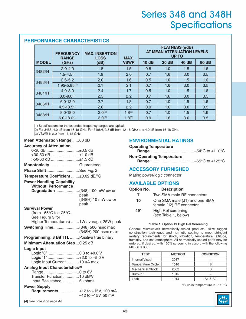
Series 348 and 348H8 Bit Digital/Analog Attenuators
Series 348 and 348HThe Series 348 and 348H Digitally Programmable Attenuators provide greater than octave band performance in small hermetic packages ideally suited for high reliability applications. The Series 348 offers moderate power handling capability (100 mW) at switching speeds less than 500 nsec while the 348H Series offers 200 nsec switching speed at lower power. Attenuation of all units is 60 dB with monotonic 0.25 dB step resolution.The attenuator is an integrated assembly of a sealed RF Microwave Integrated Circuit assembly and a sealed hybrid driver. Attenuation is controlled via a miniature 14 pin connector. See Fig. 1.Although these units are primarily intended for use as digital attenuators, they can also be used as analog (voltage driven) attenuators or as combination analog/digital attenuators. (See note 4 on page 44.)
3484
• 2 to 18 GHz• Digital/Analog• 8 Bit TTL • Hermetically sealed • Miniature
43
Series 348 and 348HSpecifications
PERFORMANCE CHARACTERISTICS
(1) Specifications for the extended frequency ranges are typical.(2) For 3488, 4.0 dB from 16-18 GHz. For 3488H, 3.5 dB from 12-16 GHz and 4.0 dB from 16-18 GHz.(3) VSWR is 2.0 from 16-18 GHz.
Mean Attenuation Range ......60 dBAccuracy of Attenuation 0-30 dB .............................±0.5 dB >30-50 dB .........................±1.0 dB >50-60 dB .........................±1.5 dBMonotonicity ..........................GuaranteedPhase Shift .............................See Fig. 2Temperature Coefficient .......±0.02 dB/°CPower Handling Capability Without Performance
Degradation ..................... (348) 100 mW cw or peak (348H) 10 mW cw or peak
Survival Power (from –65°C to +25°C.
See Figure 3 for Higher Temperatures) ....... 1W average, 25W peak
Switching Time ....................... (348) 500 nsec max (348H) 200 nsec max
Programming: 8 Bit TTL ........ Positive true binaryMinimum Attenuation Step ...0.25 dBLogic Input Logic “0” ...........................0.3 to +0.8 V Logic “1” ............................+2.0 to +5.0 V Logic Input Current ...........10 µA maxAnalog Input Characteristics(4)
Range ...............................0 to 6V Transfer Function ..............10 dB/V Input Resistance ...............6 kohmsPower Supply Requirements .................. +12 to +15V, 120 mA
–12 to –15V, 50 mA
ENVIRONMENTAL RATINGSOperating Temperature Range ....................................... –54°C to +110°CNon-Operating Temperature Range ....................................... –65°C to +125°C
ACCESSORY FURNISHEDMating power/logic connector
AVAILABLE OPTIONS Option No. Description 7 Two SMA male RF connectors 10 One SMA male (J1) and one SMA
female (J2) RF connector 49* High Rel screening
(see Table 1, below)
*Table 1. Option 49 High Rel Screening
General Microwave’s hermetically-sealed products utilize rugged construction techniques and hermetic sealing to meet stringent military requirements for shock, vibration, temperature, altitude, humidity, and salt atmosphere. All hermetically-sealed parts may be ordered, if desired, with 100% screening in accord with the following MIL-STD 883:
TEST METHOD CONDITION
Internal Visual 2017 –
Temperature Cycle 1010 B
Mechanical Shock 2002 B
Burn-In* 1015 –
Leak 1014 A1 & A2
*Burn-in temperature is +110°C
MODEL
FREQUENCY RANGE (GHz)
MAX. INSERTION LOSS (dB)
MAX. VSWR
FLATNESS (±dB) AT MEAN ATTENUATION LEVELS
UP TO
10 dB 20 dB 40 dB 60 dB
3482/H2.0-4.0 1.8 1.5 0.5 1.0 1.5 1.6
1.5-4.5(1) 1.9 2.0 0.7 1.6 3.0 3.5
3483/H2.6-5.2 2.0 1.6 0.5 1.0 1.5 1.6
1.95-5.85(1) 2.1 2.1 0.7 1.6 3.0 3.5
3484/H4.0-8.0 2.4 1.7 0.5 1.0 1.5 1.6
3.0-9.0(1) 2.5 2.2 0.7 1.6 3.0 3.5
3486/H6.0-12.0 2.7 1.8 0.7 1.0 1.5 1.6
4.5-13.5(1) 2.8 2.2 0.9 1.6 3.0 3.5
3488/H8.0-18.0 3.0(2) 1.8(3) 0.7 1.0 1.5 1.6
6.0-18.0(1) 3.0(2) 1.8(3) 0.9 1.6 3.0 3.5
(4) See note 4 on page 44

44
Series 348 and 348H Specifications
DIMENSIONS AND WEIGHT
NOTES:
1. All unused logic inputs must be grounded.
2. For normal TTL programming control, PIN B must be grounded or at Logic 0. Application of Logic 1 to PIN B overrides the digital input and sets the unit to insertion loss. To interface with other logic families (e.g., CMOS, MTL, NMOS, etc.) contact factory.
3. If Analog input is not to be used, then connect PIN R to PIN P.
4. To use the unit as a voltage controlled attenuator, apply a control voltage of 0 to +6V at PIN R. The slope of attenuation will be nominally 10 dB/V. For a non-zero source resistance (RO) of up to 500 ohms, the attenuation error is approximately –.0017 • RO • VIN dB and the slope will decrease by approximately 0.17 dB/V per 100 ohms of source resistance.
Using the 348/H Series attenuator as both a digital and analog control attenuator, the total attenuation ATT = 10 • VIN + programmed digital attenuation. The maximum attainable mean attenuation is 60 dB.
CONN. 14 PIN IAW MIL-C-28748
CONTINENTAL CONN. CO. MSMM 14-22PD91045 OR EQUIVALENT
Dimensional Tolerances, unless otherwise indicated: .XX ±.02; .XXX ±.005
J3 POWER/LOGIC CONNECTIONS
PIN FUNCTIONS
A B CD E F H J K L M N P R
Digital/Power GND Logic Control (Note 2)
–12 to –15V 0.25 dB (LSB)
0.5 dB 1 dB 4 dB 2 dB 16 dB
32 dB (MSB) +12 to +15V
8 dB GND
Analog Input (Notes 3&4)

45
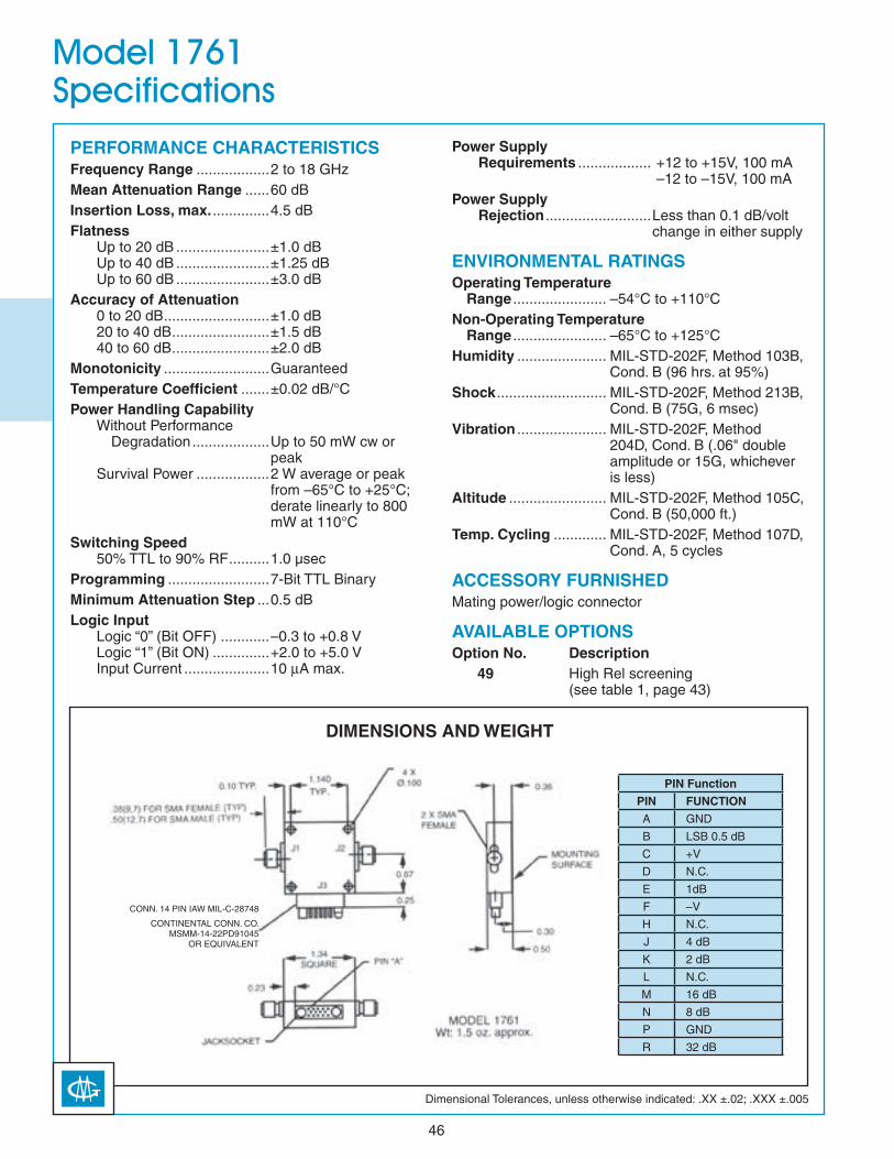
Model 1761 Multi-Octave Digitally ControlledMiniature PIN Diode Attenuator
Model 1761 is a miniaturized, digitally controlled PIN diode attenuator covering the instantaneous frequency range of 2 GHz to 18 GHz. This model, measuring only 1.34” square and 0.5” thick, provides a monotonic attenuation range of 60 dB with 7-bit (0.5 dB LSB) resolution and 1 microsecond switching speed.The Model 1761 is an integrated assembly of a dual PIN diode attenuator and a driver circuit consisting of a D/A converter and voltage-to-current converter. The unit is fully temperature compensated. The RF circuit consists of two wide band, T-pad attenuator sections in tandem. The levels of series and shunt currents required to maintain bilateral match at all frequencies is provided by the driver. This arrangement assures monotonicity over the full 2 to 18 GHz operating band at all levels of attenuation and for any programmed attenuation step.The Model 1761 weighs approximately 1.5 oz. It is configured with SMA female RF connectors and a multipin connector for logic and power. The unit is powered by ±12 to 15V DC and the logic input is TTL compatible.
• Miniature• 2 to 18 GHz • 7 Bit TTL• Hermetically sealed
46
Model 1761Specifications
PERFORMANCE CHARACTERISTICSFrequency Range ..................2 to 18 GHzMean Attenuation Range ......60 dBInsertion Loss, max. ..............4.5 dBFlatness Up to 20 dB .......................±1.0 dB Up to 40 dB .......................±1.25 dB Up to 60 dB .......................±3.0 dBAccuracy of Attenuation 0 to 20 dB ..........................±1.0 dB 20 to 40 dB ........................±1.5 dB 40 to 60 dB ........................±2.0 dBMonotonicity ..........................GuaranteedTemperature Coefficient .......±0.02 dB/°CPower Handling Capability Without Performance Degradation ................... Up to 50 mW cw or
peak Survival Power .................. 2 W average or peak
from –65°C to +25°C; derate linearly to 800 mW at 110°C
Switching Speed 50% TTL to 90% RF ..........1.0 µsecProgramming ......................... 7-Bit TTL BinaryMinimum Attenuation Step ...0.5 dBLogic Input Logic “0” (Bit OFF) ............–0.3 to +0.8 V Logic “1” (Bit ON) ..............+2.0 to +5.0 V Input Current .....................10 µA max.
Power Supply Requirements .................. +12 to +15V, 100 mA
–12 to –15V, 100 mAPower Supply Rejection .......................... Less than 0.1 dB/volt
change in either supply
ENVIRONMENTAL RATINGSOperating Temperature Range ....................... –54°C to +110°CNon-Operating Temperature Range ....................... –65°C to +125°CHumidity ...................... MIL-STD-202F, Method 103B,
Cond. B (96 hrs. at 95%)Shock ........................... MIL-STD-202F, Method 213B,
Cond. B (75G, 6 msec)Vibration ...................... MIL-STD-202F, Method
204D, Cond. B (.06" double amplitude or 15G, whichever is less)
Altitude ........................ MIL-STD-202F, Method 105C, Cond. B (50,000 ft.)
Temp. Cycling ............. MIL-STD-202F, Method 107D, Cond. A, 5 cycles
ACCESSORY FURNISHEDMating power/logic connector
AVAILABLE OPTIONS Option No. Description 49 High Rel screening
(see table 1, page 43)
DIMENSIONS AND WEIGHT
CONN. 14 PIN IAW MIL-C-28748
CONTINENTAL CONN. CO. MSMM-14-22PD91045
OR EQUIVALENT
Dimensional Tolerances, unless otherwise indicated: .XX ±.02; .XXX ±.005
PIN Function
PIN FUNCTION
A GND
B LSB 0.5 dB
C +V
D N.C.
E 1dB
F –V
H N.C.
J 4 dB
K 2 dB
L N.C.
M 16 dB
N 8 dB
P GND
R 32 dB
47
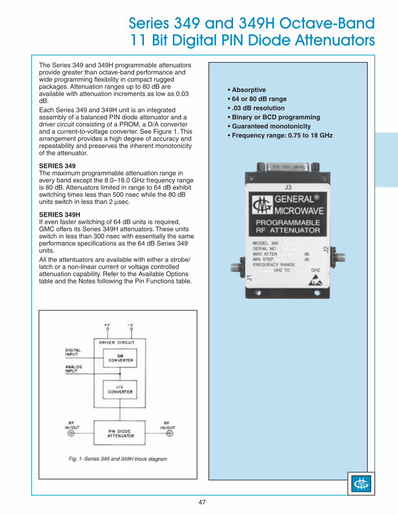
Series 349 and 349H Octave-Band11 Bit Digital PIN Diode Attenuators
The Series 349 and 349H programmable attenuators provide greater than octave-band performance and wide programming flexibility in compact rugged packages. Attenuation ranges up to 80 dB are available with attenuation increments as low as 0.03 dB.Each Series 349 and 349H unit is an integrated assembly of a balanced PIN diode attenuator and a driver circuit consisting of a PROM, a D/A converter and a current-to-voltage converter. See Figure 1. This arrangement provides a high degree of accuracy and repeatability and preserves the inherent monotonicity of the attenuator.
SERIES 349 The maximum programmable attenuation range in every band except the 8.0–18.0 GHz frequency range is 80 dB. Attenuators limited in range to 64 dB exhibit switching times less than 500 nsec while the 80 dB units switch in less than 2 µsec.
SERIES 349HIf even faster switching of 64 dB units is required, GMC offers its Series 349H attenuators. These units switch in less than 300 nsec with essentially the same performance specifications as the 64 dB Series 349 units.All the attentuators are available with either a strobe/latch or a non-linear current or voltage controlled attenuation capability. Refer to the Available Options table and the Notes following the Pin Functions table.
• Absorptive• 64 or 80 dB range • .03 dB resolution • Binary or BCD programming• Guaranteed monotonicity • Frequency range: 0.75 to 18 GHz

48
Series 349 and 349HSpecifications
PERFORMANCE CHARACTERISTICS: SERIES 349
PERFORMANCE CHARACTERISTICS: SERIES 349H
MODELFREQUENCY
RANGEGHz
MAX.INSERTIONLOSS (dB)
MAX. VSWR
FLATNESS (±dB) AT MEAN ATTENUATION LEVELS
UP TO10 dB 20 dB 40 dB 60 dB(4) 80 dB(1)
3491-64 3491-80
1.0-2.0 1.6 1.5 0.3 0.8 1.5 1.6 1.9
0.75-2.25(2) 1.7 2.0 0.5 1.4 3.0 3.5 3.8
3492-64 3492-80
2.0-4.0 1.8 1.5 0.3 0.8 1.5 1.6 1.9
1.5-4.5(2) 1.9 2.0 0.5 1.4 3.0 3.5 3.8
3493-64 3493-80
2.6-5.2 2.0 1.6 0.3 0.8 1.5 1.6 1.9
1.95-5.85(2) 2.1 2.1 0.5 1.4 3.0 3.5 3.8
3494-64 3494-80
4.0-8.0 2.4 1.7 0.3 0.8 1.5 1.6 1.9
3.0-9.0(2) 2.5 2.2 0.5 1.4 3.0 3.5 3.8
3495-64 3495-80
5.0-10.0 2.6 1.7 0.5 0.9 1.5 1.6 1.9
3.75-11.25(2) 2.7 2.2 0.7 1.4 3.0 3.5 3.8
3496-64 3496-80
6.0-12.0 2.7 1.8 0.7 1.0 1.5 1.6 1.9
4.5-13.5(2) 2.8 2.2 0.9 1.5 3.0 3.5 3.8
3498-648.0-18.0 3.0(3) 1.8(3) 0.7 1.0 1.5 1.6 —
6.0-18.0(2) 3.0(3) 1.8(3) 0.9 1.5 3.0 3.5 —
MODELFREQUENCY
RANGEGHz
MAX.INSERTIONLOSS (dB)
MAX. VSWR
FLATNESS (±dB) AT MEAN ATTENUATION LEVELS
UP TO10 dB 20 dB 40 dB 60 dB(4)
3491H-641.0-2.0 1.6 1.5 0.5 1.0 1.5 1.6
0.75-2.25(2) 1.7 2.0 0.7 1.6 3.0 3.5
3492H-642.0-4.0 1.8 1.5 0.5 1.0 1.5 1.6
1.5-4.5(2) 1.9 2.0 0.7 1.6 3.0 3.5
3493H-642.6-5.2 2.0 1.6 0.5 1.0 1.5 1.6
1.95-5.85(2) 2.1 2.1 0.7 1.6 3.0 3.5
3494H-644.0-8.0 2.4 1.7 0.5 1.0 1.5 1.6
3.0-9.0(2) 2.5 2.2 0.7 1.6 3.0 3.5
3495H-645.0-10.0 2.6 1.7 0.7 1.0 1.5 1.6
3.75-11.25(2) 2.7 2.2 0.9 1.6 3.0 3.5
3496H-646.0-12.0 2.7 1.8 0.7 1.0 1.5 1.6
4.5-13.5(2) 2.8 2.2 0.9 1.6 3.0 3.5
3498H-648.0-18.0 3.0(3) 1.8(3) 0.7 1.0 1.5 1.6
6.0-18.0(2) 3.0(3) 1.8(3) 0.9 1.6 3.0 3.5
(1) Applicable only to 80 dB versions.
(2) Specifications for the extended frequency ranges are typical.
(3) Except from 16-18 GHz where insertion loss is 4.2 dB max. and VSWR is 2.2.
(4) Flatness specification at 64 dB level is ±0.2 dB higher than at 60 dB.

49
Series 349 and 349HSpecifications
Mean Attenuation Range 349(x)-64, 349(x)H-64 .............. 64 dB 349(x)-80 .................................. 80 dBAccuracy of Attenuation 0-30 dB ................................... ±0.5 dB >30-50 dB ................................ ±1.0 dB >50-64 dB ................................ ±1.5 dB >64-80 dB ................................ ±2.0 dBMonotonicity ................................. GuaranteedTemperature Coefficient .............. ±0.025 dB/°CPower Handling Capability Without Performance Degradation 3491, 3492H thru 3498H ... 10 mW cw or peak 3491H ................................ 1 mW cw or peak All other units ..................... 100 mW cw or peak Survival Power (from –40˚C to +25˚C;
see figure 2 for higher temperatures) All units .............................. 1 W average 25 W
peak (1 µsec max pulse width)
Switching Time 349(x)H-64 ............................... 300 nsec max. 349(x)-64 .................................. 500 nsec max. 349(x)-80 .................................. 2 µsec maxProgramming ................................ Positive true binary
(standard) or BCD (Option 1). For complementary code, specify Option 2.
Minimum Attenuation Step(1)
Binary Units 349(x)-64, 349(x)H-64 ....... 0.03 dB 349(x)-80 ........................... 0.04 dB BCD Units ................................ 0.10 dBLogic Input Logic “0” (Bit OFF) ................... –0.3 to +0.8 V Logic “1” (Bit ON) ..................... +2.0 to +5.0 V Logic Input Current .................. 1 µA max.Analog Input 349(x)-64, 349(x)H-64 .............. 0 to 6.4 V 349(x)-80 .................................. 0 to 8 V Input Resistance ...................... 10 K ohmsPower Supply Requirements ......................... +12 to +15V, 120 mA
–12 to –15V, 50 mAPower Supply Rejection ................................. Less than 0.1 dB/volt
change in either supply
ENVIRONMENTAL RATINGSOperating Temperature Range .............................. –40°C to +85°CNon-Operating Temperature Range ........ –54°C to +100°CHumidity ............................. MIL-STD-202F, Method
103B, Cond. B (96 hrs. at 95%)
Shock .................................. MIL-STD-202F, Method 213B, Cond. B (75G, 6 msec)
Vibration ............................. MIL-STD-202F, Method 204D, Cond. B (.06" double amplitude or 15G, whichever is less)
Altitude ............................... MIL-STD-202F, Method 105C, Cond. B (50,000 ft.)
Temp. Cycling .................... MIL-STD-202F, Method 107D, Cond. A, 5 cycles
ACCESSORIES FURNISHEDMating power/logic connector
AVAILABLE OPTIONS Option No. Description 1 BDC programming (Binary is standard) 2 Complementary programming
(logic “0” is Bit ON) 4 Strobe latch for data input. Attenuator
responds to data input when logic “0” is applied. Attenuator latched to data input when logic “1” is applied
7 Two SMA male RF connectors 10 One SMA male RF connector (J1) and
one SMA female RF connector (J2)
(1) See note 3 on page 50

50
Series 349 and 349HSpecifications
DIMENSIONS AND WEIGHTS
NOTES
1. Normally supplied as an Analog input. Leave pin open if analog input is not used. Optionally available as a strobe latch function for input data.
2. Pin 3 is available to apply a current or voltage to control the attenuator in a non-linear fashion.
3. The Series 349 attenuators are 11-bit digital attenuators. In order to use this device with a lesser number of bits (lower resolution), the user may simply ground the logic pins for the lowest order unused bits. For example, a Series 349 unit operated as an 8-bit unit would have Pin 15, Pin 1 and Pin 2 connected to ground. All other parameters remain unchanged.
Dimensional Tolerances, unless otherwise indicated: .XX ±.02; .XXX ±.005
MODEL DIM “A” DIM “B” DIM “C” DIM “D” DIM “E” DIM “F”
3491, 3491H
.58 (14,7)
.42 (10,7)
2.56 ± .03 (65,0)
.56 (14,2)
1.53 (38,9)
.34 (8,6)
3492, 93, 3492H, 93H
.30 (7,6)
.14 (3,6)
2.00 ± .03 (50,8)
.50 (12,7)
1.29 (32,8)
.34 (8,6)
3494, 95, 96 3494H, 95H, 96H
.30 (7,6)
.14 (3,6)
2.00 ± .03 (50,8)
.75 (19,1)
1.19 (30,2)
.34 (8,6)
3498, 3498H
.30 (7,6)
.14 (3,6)
2.00 ± .03 (50,8)
.75 (19,1)
1.00 (25.4)
.34 (8,6)
J3 PIN FUNCTIONS(3)
PINBINARY
BCD64 dB 80 dB
1 0.06 dB 0.08 dB 0.2 dB 2 0.13 dB 0.16 dB 0.4 dB 3 Analog Input / Strobe Latch(1)(2)
4 GND
5 0.25 dB 0.31 dB 0.8 dB
6 0.5dB 0.63 dB 1 dB 7 1 dB 1.25 dB 2 dB 8 2 dB 2.5 dB 4 dB 9 4 dB 5 dB 8 dB10 8 dB 10 dB 10 dB11 16 dB 20 dB 20 dB12 32 dB 40 dB 40 dB13 +12 to +15V14 –12 to –15V15 0.03 db 0.04 dB 0.1 dB