atsuhiko ochi kobe university - cern
TRANSCRIPT

Atsuhiko OchiKobe University
RD51 mini-week@CERN 08/06/2015

Resistive electrodes is one of best choice for reducing the sparks on MPGDs.
However, it is not easy to find the “resistive material” for Micro Pattern.
In case, surface resistivity of 1MΩ/sq. is needed; In general, the electrodes for MPGDs has 0.1µm – 10µm thickness. Those correspond to bulk resistivity of 0.1Ωm-10Ωm.
10-8 10-7 10-6 10-5 10-4 10-3 10-2 10-1 100 101 102 103 104 105 106 107 108 109 1010 10111012 1013 1014 1015 1016
AgCuAuAlCoNiFeCr
PbTiMnStainless
HgNichrome
Graphite
SiPaper
Water
P
WoodGlass
Mica
SGe
Suitable zone for resistive MPGDs
Very few materials meetsour requirement
08/06/2015A.Ochi RD51 mini week @ CERN 2
[Ωm]

Carbon black loaded paste/sheet have been used for resistive material Carbon black: small particles, made from mainly graphite. Those are used by mixing in plastic, epoxy, solvant etc. Mechanism of resistivity development
Carbon black particles contact each other on point, and it makes electrical path.
We need very small carbon black particles for fine structure of MPGD electrodes.
08/06/2015A.Ochi RD51 mini week @ CERN 3

Sputtered carbon Diamond like, and amorphous
structure It means, carbon particles of
molecular size! Fine structure with proper
resistivity is available with liftoff method
Substrate (polyimide)
Photo resist(reverse pattern of surface strips)
Substrate (polyimide)
Carbon spattering
Substrate (polyimide)
Developing the resists
408/06/2015A.Ochi RD51 mini week @ CERN

The structure of the sputtered carbon is amorphous diamond like carbon (a-DLC).
It is thought that the charge carrier is very few in the DLC
So, I got an idea of nitrogen doping as a supplier of carrier electrons. This is same story as the n-type
semiconductor production. The nitrogen is easy to introduce
into the sputtering chamber with Argon gas.
08/06/2015A.Ochi RD51 mini week @ CERN 5
Vacuum chamber(with Ar + N2 gas)
Rotating drum4.5 m round
Sample
Sputteringtarget
C C
Dope
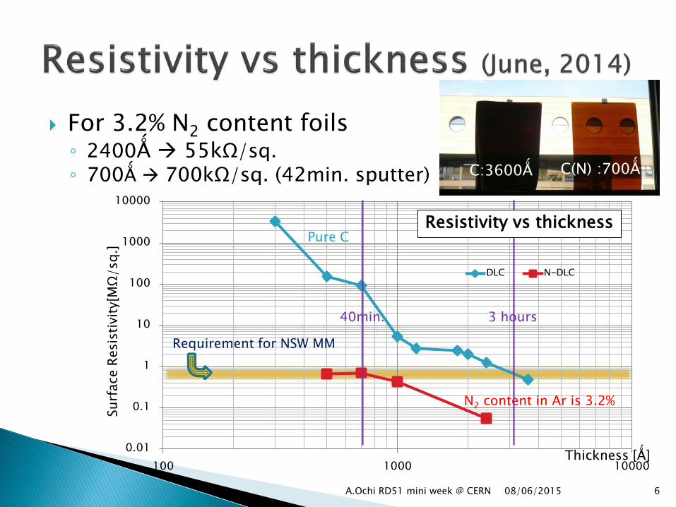
For 3.2% N2 content foils 2400Ǻ 55kΩ/sq. 700Ǻ 700kΩ/sq. (42min. sputter)
08/06/2015A.Ochi RD51 mini week @ CERN 6
0.01
0.1
1
10
100
1000
10000
100 1000 10000
DLC N-DLC
Surf
ace
Resi
stiv
ity[M
Ω/s
q.]
Thickness [Ǻ]
N2 content in Ar is 3.2%
Requirement for NSW MM
40min. 3 hours
Resistivity vs thicknessPure C
C:3600Ǻ C(N) :700Ǻ

Properties of the resistive electrodes by carbon sputtering Fine structure Chemical and physical toughness Very thin (50nm – 500nm) Large area is aveilable
We have made following resistive MPGDs using carbon sputtering MicroMEGASGEMMSGCMicro-PIC
Be-Sputter Co. Ltd.(Kyoto Japan)
08/06/2015A.Ochi RD51 mini week @ CERN 7

First attempt to make MPGDs using carbon sputtering (from June 2013) This R&D is aimed for ATLAS
NSW MM. Fine strip pitch of 200 μm or
400 μm is formed on 50μm polyimide foil.
08/06/2015A.Ochi RD51 mini week @ CERN 8
Flexible foil (polyimide)
Rigid PCB (epoxy)
Resistive strips (sputtered)
Readout stripsBonding film
Mesh
Pillar
25μm
35μm
Substrate (polyimide)
Carbon (300-600Å)

08/06/2015 9A.Ochi RD51 mini week @ CERN
(March 2015)

08/06/2015A.Ochi RD51 mini week @ CERN 10
10 mm
1 mm
0.3 mm

Resistive MM for ATLAS NSW Technology for Large area and series production have
been established. There are many reports on operation tests. However, production cost using screen printing is less
than half, our first choice for resistive strip in NSW is screen printing. Requirement on the ATLAS MM resistive strips are not so fine
that printing technology is enough. Other MM with carbon sputter We have provided planner carbon sputtered foil for
prototype of ILC-TPC MicroMEGAS . Paul will talk “Diamond like carbon MM” in next talk.
08/06/2015A.Ochi RD51 mini week @ CERN 11

Standard type GEM (holes with 140µm pitch, diameter with 70-85µm.) with resistive electrodes.
The resistive electrodes are made by very thin (~100nm) sputtered carbon It will improve the signal gain Surface resistivity ~ 1MΩ/sq.
Holes are made by laser drilling
50 - 100µmSubstrate
Sputteredcarbon
08/06/2015A.Ochi RD51 mini week @ CERN 12

Previous study: (RIKEN RE-GEM, A. Yoshikawa et.
al., 2012 JINST 7 C06006) Resistive electrodes are made
from resistive sheet with 25µm thickness.
In the simulation study, avalanched electrons cross over the thick resistive electrodes.
Our prospects: Sputtered electrodes are very thin Avalanched electrons will not be
interfered by electrodes.
08/06/2015A.Ochi RD51 mini week @ CERN 13

RE-GEM was set as one layer of triple GEM Other layer is standard GEM
Signals with RE-GEM were compared to that without RE-GEM for obtain gas gain
300ns
300mV
08/06/2015A.Ochi RD51 mini week @ CERN 14

drift: 370GEM1: 370Transfer1: 370GEM2: 370Transfer2: 370GEM3: 280Induction: 747
28.92
GEM3: 250~290V
Those are all preliminary dataDevelopments and tests are ongoing!!
08/06/2015A.Ochi RD51 mini week @ CERN 15
(April, 2015)

To study basic properties of fine structure MPGD, prototype of RE-MSGC using carbon sputter have been made.
4 geometry with 2 different anode materials are made
20
180
100 φ300
400
100 mm
5 mm
銅パターン3 mm
3 mm
Cu
Carbon sputter
20
400
100 mm
5 mm
銅パターン3 mm
3 mm
Cu
Carbon sputter
120 30
φ14060
20
400
100 mm
5 mm
銅パターン3 mm
3 mm
Cu
Carbon sputter
80 50
φ14060
20
280
100 φ300
400
100 mm
5 mm
銅パターン3 mm
3 mm
Cu
Carbon sputter
50
08/06/2015A.Ochi RD51 mini week @ CERN 16

Signal is read from back strip (induced carge) Gain variation along the time is found There are alignment problem between copper
anode and sputtered cathode. Those electrodes are made by different masks
Those researches are just started, and ongoing
time [min]
Puls
e he
ight
(arb
.uni
ts)
① |Va|:|Vc| = 8 : 1② |Va|:|Vc| = 7 : 2③ |Va|:|Vc| = 6 : 3
08/06/2015A.Ochi RD51 mini week @ CERN 17
(June, 2015)

The cathodes of µ-PIC is formed by resistive material. Large current from spark reduce the e-field, and
spark is quenched. Signal from low energy deposit will observed with
higher gas gain This design provide one promised possibility of MIP
detector under hadronic background It takes enough gain
(~7 x 10⁵ , with Ar+ethane)
Drift plane
Anode
Resistive cathode (-HV)
Pickup electrode
Thinsubstrate
400 μm
Thick substrate 50 μm08/06/2015A.Ochi RD51 mini week @ CERN 18

08/06/2015A.Ochi RD51 mini week @ CERN 19
HV current on anodes are monitored while neutrons are irradiated
We found strong spark reduction using resistive cathode !!
Normal µ-PIC (metal cathodes)Gain = 15000Irradiation: 2.4×10³ neutron/sec
Resistive cathode µ-PIC Gain = 15000irradiation: 1.9×10⁶ neutron/sec
[µA]10
8
6
4
2
0
[µA]10
8
6
4
2
0
neutron
Drift
-HV(~1kV)
Cathode= 0V
A+HV(~600V)
AnodeVoltage recorder

Cathode structure should be fine
Sputtering with liftoff is very good method for those structures.
Prototype was made, however, it has not operated yet. Some problems for
alignment of multi layer
08/06/2015A.Ochi RD51 mini week @ CERN 20

Carbon sputtering : Very fine and stable way for MPGD electrodes! Less than 10µm structure Tough chemically and physically
Resistivity control Available from a few kΩ/sq. to several tens MΩ/sq. using N dope
method and thickness control Carbon sputter for MPGDs MicroMEGAS (resitive strip) Technology has already been established. Large area (~ a few m2) with
mass production is available GEM: Prototype has been worked. On going. MSGC: Prototype has been worked. µ-PIC Principle operation has been checked with other resistive material. Prototype production using carbon sputtering is ongoing.
Carbon sputtering is very promising way for new structures of MPGDs!!
08/06/2015A.Ochi RD51 mini week @ CERN 21