atomic’scale’defects:’’ probing’structure’and’func8on’ ·...
TRANSCRIPT

Atomic Scale Defects: Probing Structure and Func8on
Felix Hofmann Department of Engineering Science, University of Oxford, UK.

Warwick Nov 2017 [email protected] 2
Kiener et al. Nat. Mater. (2011)
Sand et al., EPL (2013)
3D – 0D
X. Yi et al., arXiv: 1503.02922v1 (2015)
1D
Hardie et al., JNM (2014)
Yang et al., J Cryst Growth (2011)
Atomic Scale Crystal Defects

Warwick Nov 2017 [email protected] 3
Measuring Defect Strain Fields
Edge dislocaYon in silicon, looking down [1-‐10] direcYon.
Atomic-‐scale images Displacement fields
Hytch et al., Nature 423 (2003)

Warwick Nov 2017 [email protected] 4
• 3D imaging of dislocaYons in the bulk
• DislocaYon posiYons
• Low dislocaYon densiYes
SyntheYc Diamond
Ludwig et al. J. Appl. Crystallography (2001)
X-‐ray topograph Etch pits (opYcal)
Silicon single crystal. 1st X-‐ray images of dislocaYons. Newkirk, Phys. Rev. (1958)
Topo-‐Tomography
X-‐ray Imaging of DislocaYons

Warwick Nov 2017 [email protected] 5
DA
DB
TEM
10 μm
[II0]
[IĪ0]
• GaAs-‐InGaAs mulYlayer. Misfit dislocaYons at GaAs-‐InGaAs interface. • Easy to see dislocaYons in TEM. • Can clearly idenYfy both dislocaYons in TEM and Laue image
In0.2Ga0.8As
y [00I]
z [ĪĪ0]
x [IĪ0]
dislocaYon
simulaYon plane
Hofmann et al. Nat. Commun. (2013)
0.6 0.4 0.2 0 -‐0.2 -‐0.4 -‐0.6
DA
DB
10 μm
Laue
[II0]
[IĪ0]
ωĪĪ0
Laice rotaYon Micro Laue
Probing Strains due to an Individual DislocaYon

Warwick Nov 2017 [email protected] 6
Deviatoric elasYc strains (x10-‐6)
εyy
εxx
εzz
Calcula8ons Measurements vs. Predic8ons
degrees
ωĪĪ0
μm
Laice rotaYons ε00I
μm
ElasYc strains x10-‐6
• Anisotropic elasYcity modelling.
• “Virtual” diffracYon experiment to predict strain and rotaYon profiles
• Good agreement between predicYon and measurement
Hofmann et al. Nat. Commun. (2013)
In0.2Ga0.8As
z [ĪĪ0]
x [IĪ0]
dislocaYon
simulaYon plane
Probing Strains due to an Individual DislocaYon

Warwick Nov 2017 [email protected] 7
• IntroducYon • Point Defects
IrradiaYon-‐Induced Defects, Laice Swelling, Modulus Change, Thermal Transport, DFT, MD, Defect EvoluYon, InteracYon with DislocaYons
• Ion-‐Machining Damage Coherent X-‐ray DiffracYon Imaging, Nano-‐scale Laice Strains and Crystal Defects
• Conclusions
Outline

Warwick Nov 2017 [email protected] 8
Sand et al., Europhysics Leoers (2013)
• High fusion neutron flux1 (up to ~1015 n cm-‐2 s-‐1 per lethargy interval at 14.1 MeV) -‐> collision cascade damage and transmutaYon alloying
• High operaYng temperatures (up to ~1500K) • Intense flux of helium and hydrogen ions and neutrals (up to ~15 MW m-‐1)
-‐> high heat loading and implantaYon-‐modified structure and properYes -‐> Gas-‐Defect interac8on
Gilbert et al., Nucl. Fusion (2012)
The Tokamak
> Magnets
> Vacuum Vessel
> Blanket
> Divertor
> Diagnostics
> External Heating
> Cryostat
External Systems
> CODAC
> Vacuum System
> Cryogenics
> Remote Handling
> Power Supply
> Fuel Cycle
> Hot Cell
> Cooling Water
> Tritium Breeding
Comments & questions should be addressed to [email protected].© 2015, ITER Organization | Terms of use
ITER: the world's largest Tokamak
ITER is based on the 'tokamak' concept of magnetic confinement, in which the plasma is contained in a doughnut-shaped vacuum vessel. The fuel—a mixture of deuterium and tritium, two isotopes of hydrogen—is heated totemperatures in excess of 150 million°C, forming a hot plasma. Strong magnetic fields are used to keep the plasmaaway from the walls; these are produced by superconducting coils surrounding the vessel, and by an electrical currentdriven through the plasma. Scroll over the machine with your cursor to identify the different parts of the machine.
Transport GlossaryConstruction The Machine The Science The Organization The Project General Information
iter.orgsearch:
Search
www.iter.org/
Tungsten for Plasma-‐Facing Fusion Armour
150 keV cascade in W. Colour coded by Yme red 0fs, blue 200 fs

Warwick Nov 2017 [email protected] 9
• Ion-‐implantaYon of annealed UHP tungsten at 300°C: • 3000 appm Helium implantaYon,
mulYple energies max. 2 MeV • 2 MeV W+ at 300°C • sequenYal implantaYon
W+ then He+
• Small change in hardness due to self ion damage
• Large apparent change in hardness due to helium implantaYon
Armstrong et al., APL 102 (2013)
The “Helium Effect” -‐> Nano-‐IndentaYon

Warwick Nov 2017 [email protected] 10
• Pure W + 3000 appm He, 1μm under-‐focus
• No bubbles or other defects visible
• Storage in vacancies -‐> Positron annihilaYon can probe vacancies and vacancy complexes [Debelle JNM 362 (2007) 181-‐188; Lhuillier JNM 416 2011 13-‐17].
Quan8fying defect numbers is challenging. Lack of spa8al resolu8on.
Armstrong et al., APL 102 (2013)
Helium-‐Implanted Tungsten: TEM
Warwick Nov 2017 [email protected] 11
0.0
0.1
0.2
0.3
0.4
0.5
0.6
0
1
2
3
4
5
0.0 1.0 2.0 3.0
displacemen
t dam
age (dpa
)
heliu
m con
centra8o
n (app
m)
depth into sample (µm)
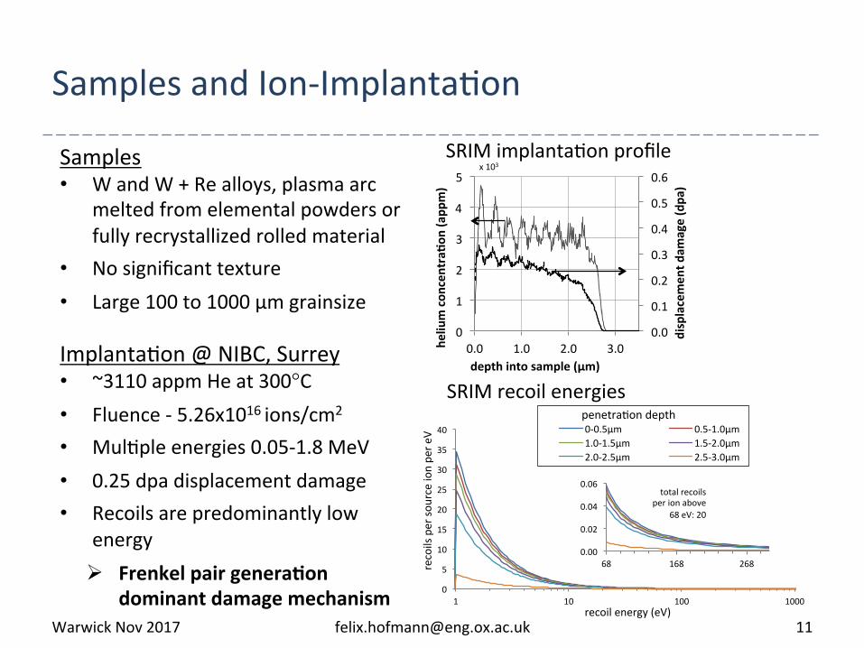
Samples • W and W + Re alloys, plasma arc
melted from elemental powders or fully recrystallized rolled material
• No significant texture • Large 100 to 1000 μm grainsize
ImplantaYon @ NIBC, Surrey • ~3110 appm He at 300°C • Fluence -‐ 5.26x10¹⁶ ions/cm2
• MulYple energies 0.05-‐1.8 MeV • 0.25 dpa displacement damage • Recoils are predominantly low
energy Ø Frenkel pair genera8on
dominant damage mechanism 0
5
10
15
20
25
30
35
40
1 10 100 1000
recoils per so
urce ion pe
r eV
recoil energy (eV)
0-‐0.5µm 0.5-‐1.0µm 1.0-‐1.5µm 1.5-‐2.0µm 2.0-‐2.5µm 2.5-‐3.0µm
penetraYon depth
0.00
0.02
0.04
0.06
68 168 268
total recoils per ion above
68 eV: 20
x 103 SRIM implantaYon profile
SRIM recoil energies
Samples and Ion-‐ImplantaYon

Warwick Nov 2017 [email protected] 12
calculated implanted depth
εzz
Elas8c strain vs. depth in sample
• DifferenYal Aperture X-‐ray Microscopy (DAXM) -‐> ~1 μm 3D strain resoluYon
• In-‐plane strains (εxx & εyy ) ~ 0 -‐> No bubbles upon implantaYon
• εzz large in implanted layer -‐> Laice swelling
How can this laOce swelling be related to internal defects?
εv =3(1−ν )(1+ν )
ε zz = 2620 ± 200( )×10−6
Hofmann et al. Acta Mater. 89 (2015)
White or Mono X-‐rays
K-‐B Mirrors
Area Detector
Sample
DifferenYal Aperture
x y z
X
X-‐ray Beam
Sample
Micro-‐beam Laue diffrac8on, 34IDE @ APS
Defect-‐Induced Laice Swelling

Warwick Nov 2017 [email protected] 13
• Laice swelling due to implantaYon-‐induced defects:
• Introduce defects within a 4 x 4 x 4 tungsten bcc supercell -‐> 128 atoms Vacancies (Vn), self intersYYal atom (SIA), intersYYal helium clusters (Hen), helium vacancy clusters (HenV)
• Boundaries are free to expand -‐> calculate defect relaxaYon volumes:
Ωr (defect) =Ω(defect)−Ω(perfect) CalculaYon details: Perdew-‐Burke-‐Ernzerhof electron exchange-‐correlaYon funcYonal within generalized gradient approximaYon. Projector augmented wave (PAW) pseudopotenYals implemented in the Vienna Ab-‐iniYo SimulaYon Package (VASP). 400 eV plane wave cutoff energy and 4 x 4 x 4 k-‐point mesh with 0.15 Å-‐1 spacing. Periodic boundary condiYons with expansion in all direcYons allowed.
111 SIA He2V
εv = nAΩr(A)
A∑
Hofmann et al. Acta Mater. 89 (2015)
DFT CalculaYons of RelaxaYon Volume

Warwick Nov 2017 [email protected] 14
Relaxation*volumes*for*vacancies*and*self3interstitial*V! V2*(1NN)! V2*(2NN)! V2(3NN)! V3(1NN(2)+
2NN)!<111>*SIA! Frenkel*
30.37*30.34*[1]*30.38*[2]*
30.72*30.65*[1]*
30.79*30.74*[1]*
30.76*30.69*[1]*
31.08** 1.68* 1.31*
*Relaxation*volumes*for*interstitial*helium*clusters*He*(tetra)! He*(octa)! He2*(tetra)! He3*(tetra)! He4*(tetra)* He5*(tetra)* *
0.36!0.33*[3]!
0.37!0.34*[3]!
0.80! 1.16! 1.65* 2.03* *
*Relaxation*volumes*for*helium*3*vacancy*clusters*HeV*(tetra)! HeV*!
(octa)*!He2V*(tetra)*!
He3V*(tetra)!
He4V*(tetra)!
He5V*(tetra)!
He6V*(tetra)*
30.24** 30.23** *30.06** 0.14* 0.38* 0.71* 1.09**[1]* Kato*D,*Iwakiri*H,*Morishita*K.*Journal*of*Nuclear*Materials*2011;417:1115.*[2]* Heinola*K,*Ahlgren*T,*Nordlund*K,*Keinonen*J.*Physical*Review*B*2010;82:094102.*[3]* Zhou*HB,*Jin*S,*Shu*XL,*Zhang*Y,*Lu*GH,*Liu*F.*EPL*(Europhysics*Letters)*2011;96:66001.*
Ø Vacancy relaxa8on volume: small and nega8ve Ø SIA relaxa8on volume: large and posi8ve Ø Helium-‐filled vacancy relaxa8on volume: nega8ve for small n, posi8ve for large n
DFT CalculaYons of RelaxaYon Volume

Warwick Nov 2017 [email protected] 15
• EnergeYcally storage of helium in vacancy clusters is always favourable -‐> assume all helium is stored in the form of HenV complexes, prevenYng recombinaYon of Frenkel pairs.
• Swelling modes: – Shooky -‐> accumulaYon of vacancies in bulk, migraYon of SIAs to the surface -‐> would cause
some swelling, but liole laice strain
– Frenkel -‐> accumulaYons of helium-‐filled Frenkel pairs in the bulk -‐> would cause much more laice strain -‐> likely to be the acYve mechanism here.
• Consider He storage in 3110 appm HeV complexes with 3110 appm SIAs: εzz (HeV + SIA) = 2654 x 10-‐6 Ø Predict almost twice experimental εzz strain (1550 x 10-‐6)
• Consider clustering1, i.e. 1555 appm He2V complexes & 1555 appm SIAs: εzz (He2V + SIA) = 1493 x 10-‐6 Ø Good agreement with experimental εzz strain!
Hofmann et al. Acta Mater. 89 (2015) 1 De Backer et al., JNM 429:78 (2012)
Swelling Analysis

Warwick Nov 2017 [email protected] 16
• SIAs delocalise to form <111> crowdions that are highly mobile (0.05 eV migraYon energy)1
• He-‐filled vacancies may act as traps for SIAs as shown by recent MD calculaYons2, 3
1 Nguyen-‐Manh et al., Phys. Rev. B 73 (2006) 020101. 2 Sandoval et al., Phys. Rev. Leo. 114 (2015) 105502. 3 J. Boisse et al., J. Mater. Res. 29, 20 (2014).
1000 K, atoms parYcipaYng in vacancy (blue), SIA (yellow), surface adatoms (green)2
Helium in blue, W atoms coloured by energy. SIA marked by red circle, vacancy by red arrow3
Why are SIAs retained?

Warwick Nov 2017 [email protected] 17
Large scale atomis8c calcula8ons of SIA clusters
• 32 x 32 x 32 atom simulaYon cell • Marinica potenYal for tungsten1 • Randomly insert SIAs then relax • Lateral expansion is constrained
Vacancies • Immobile at 300°C implantaYon
temperature2
SIAs • <111> crowdions highly mobile at RT3 • TEM: clusters < ~60 SIAs • RelaxaYon volume scales linearly with number of SIAs in cluster Ø Clustering not expected to affect our analysis 1Marinica et al., J. Phys. Cond. Maoer 25 (2013)
2 Rasch et al. Philos. Mag. A 41 (1980) 3 Nguyen-‐Manh et al., Phys. Rev. B 73 (2006)
Ωr(SIA)
Hofmann et al. Acta Mater. 89 (2015)
The Effect of Defect Clustering

Warwick Nov 2017 [email protected] 18
• Transient graYng wavelength λ = 2.75 μm
• Surface layer of thickness λ dominates signal
• Rayleigh wave velociYes: • Unimplanted: 2680 ± 2 ms-‐1 • He-‐implanted: 2621 ± 7 ms-‐1
Ø Decrease of cr by 2.2 %
0 50 100 150 200−0.2
0
0.2
0.4
0.6
0.8
1
time (ns)Yme (ns)
intensity
(a.u.)
cr = fλ
≈ c* E2(1+ν )ρ
c* = 0.874 + 0.196ν − 0.043ν 2 − 0.055ν 3( )
0 500 1000 1500 20000
0.2
0.4
0.6
0.8
1
amplitu
de (a.u.)
frequency (MHz)
FT unimplanted
shear wave speed
ExcitaYon beam
515 nm 60ps
Sample λ
Time t = 0
ExcitaYon beam
515 nm 60ps
Sample
Reference beam
532 nm
Probe beam 532 nm
Combined probe and reference
beam Time t > 0
Hofmann et al. Acta Mater. 89 (2015)
ElasYc Property Changes

Warwick Nov 2017 [email protected] 19
• Implanted material elasYc constants (using Voigt approach)
• Calculate Rayleigh wave velocity from elasYc constants
cr ≈ 0.874 + 0.196ν − 0.043ν 2 − 0.055ν 3( ) E2(1+ν )ρ
in m/s calculated experiments Voigt Reuss
Perfect W 2667 2667 2679 W + He2V + SIAs 2622 2618 2621
Change -‐1.7% -‐1.9% -‐2.2%
Cijimplanted = (1−128(nSIA + nHe2V ))Cij
W +128nSIACijSIA +128nHe2VCij
He2V
!! ! C11!(GPa)! C12!(GPa)! C44!(GPa)! A! K!(GPa)! G!(GPa)! E!(GPa)! nu!
Pure!W! 522.8! 203.5! 160.7! 1.01! 309.9! 160.3! 410.1! 0.279!
W!+!1555!appm!He2V!+!1555!appm!SIAs!
514.4! 208.7! 155.5! 1.02! 310.6! 154.5! 397.5! 0.287!
!Modulus Poisson raYo
close to isotropic
Hofmann et al. Acta Mater. 89 (2015)
ElasYc Property Changes

Warwick Nov 2017 [email protected] 20
• <110> W single crystal, implanted with ~3000 appm He at 296 K
• SAW velocity measured as funcYon of angle from <110> direcYon
• Fit experimental data with calculated SAW velocity for elasYcally anisotropic material1
Measured increase in elas8c anisotropy in very good agreement with predic8on
<110> <110> <100> <110> <100>
implanted A = 1.028
unimplanted A = 1.014
[110]
[1-‐10]
SAW velocity direcYon
1Every et al., Ultrasonics (2016)
ElasYc Property Changes
Duncan et al. Applied Physics Leoers 109 (15), 151906

Warwick Nov 2017 [email protected] 21
Time (ns)
Intensity
(a.u.)
0 50 100 150
0
0.5
1fit
• Transient graYng background signal related to decay of thermal graYng
• Can fit this to extract thermal
diffusivity of ion-‐implanted layer:
• Probed depth ~ λ/π
Can measure the thermal diffusivity of ion-‐implanted layer! (without modifying sample surface) #10-9
0 5 10 15
0
0.2
0.4
0.6
0.8
1 WW+He
! = !erfc ! !! !!!!!!!!!!!!+! sin 2!"# + ! exp − !
! !!!!!!!!!!!!!!!!!+!.!
graYng decay
Hofmann et al. ScienYfic Reports 16042 (2015)
Thermal Transport Changes

Warwick Nov 2017 [email protected] 22
0"
0.2"
0.4"
0.6"
0.8"
1"
1.2"
100" 200" 300" 400" 500" 600" 700"
Thermal"Diffusivity
"(cm
2 /s)"
Temperature"(K)"
Pure"W"WC1%Re"WC2%Re"Pure"W"WC5%Re"WC10%Re"WC25%Re"
• Good agreement of pure W with literature data
• Reliable extracYon of thermal transport parameters by TG
• Clearly see a saturaYon effect with increasing Re content
Degrada8on of thermal transport due to transmuta8on alloying will be important (in DEMO armour 3% of Re will appear within 5 years)2
1Fujitsuka, M., Journal of Nuclear Materials 283–287 (2000) 2Gilbert et al., Nucl. Fusion 52 (2012)
Fujitsuka1
Hofmann et al. ScienYfic Reports 16042 (2015)
Thermal Transport Changes -‐> Re Effect
Warwick Nov 2017 [email protected] 23
0"
0.2"
0.4"
0.6"
0.8"
1"
1.2"
100" 200" 300" 400" 500" 600" 700"
Thermal"Diffusivity
"(cm
2 /s)!
Temperature"(K)!
Pure"W"
W"+"280"appm"He"
W"+"3100"appm"He"
Hofmann et al. ScienYfic Reports 16042 (2015)
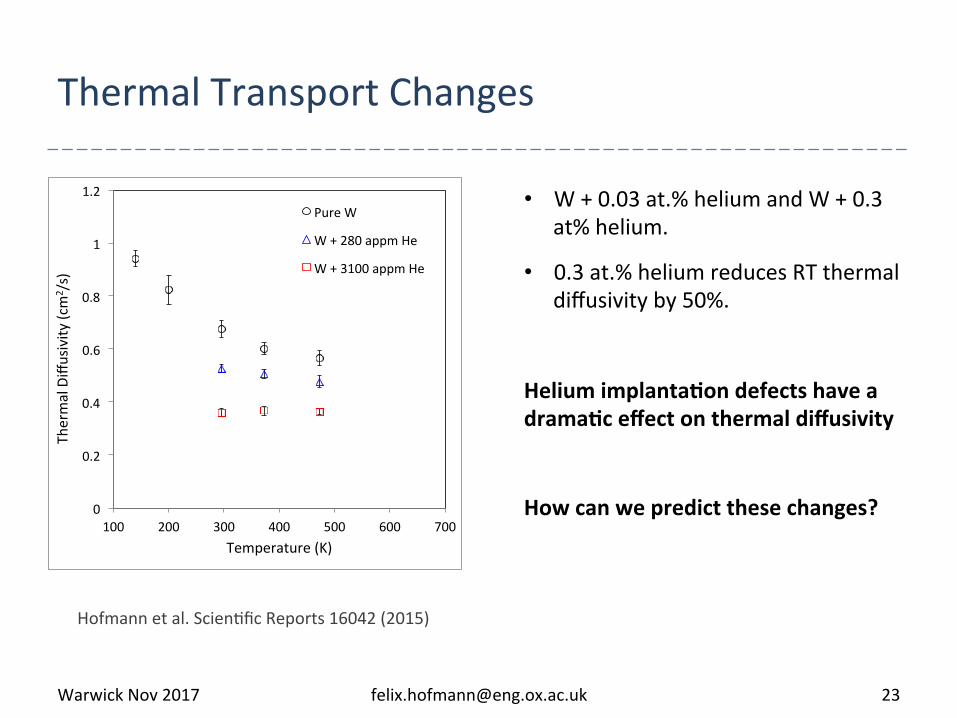
• W + 0.03 at.% helium and W + 0.3 at% helium.
• 0.3 at.% helium reduces RT thermal diffusivity by 50%.
Helium implanta8on defects have a drama8c effect on thermal diffusivity
How can we predict these changes?
Thermal Transport Changes

Warwick Nov 2017 [email protected] 24
• Use Ackland-‐The�ord EAM potenYal for tungsten1, generate defect structure, relax
• Correlate atomic energy in excess of thermal average with scaoering rate2 Ø Calibrated based on vacancy and self-‐
intersYYal electrical resisYvity
• Vacancies now appear as “cages” of 8 scaoering atoms
• Self intersYYals appear as a “string” of atoms with different scaoering strength
• Compute electronic scaoering rate by summing over all atomic sites
In principle conduc8vity for any kind of damage structure could be calculated…
Atomic sites coloured by sca1ering rate
1Ackland, The�ord, Philos. Mag. A 56 (1987). 2Mason, D. R. Journal of Physics: Condensed Maoer 27, (2015).
Hofmann et al. ScienYfic Reports 16042 (2015)
Thermal Transport Changes

Warwick Nov 2017 [email protected] 25
0"
0.2"
0.4"
0.6"
0.8"
1"
1.2"
100" 200" 300" 400" 500" 600" 700"
Thermal"Diffusivity
"(cm
2 /s)!
Temperature"(K)!
Pure"W"
W"+"280"appm"He"
W"+"3100"appm"He"
3000 Frenkel
900 Frenkel
• Predict lower thermal diffusiviYes for He-‐implanted samples: Ø 300 appm He -‐> 900 appm Frenkel
defects Ø 3000 appm He -‐> 3000 appm Frenkel
defects
• Decrease of Frenkel:He raYo with increasing dose consistent with OKMC calculaYons1
• At low doses impuriYes dominate Frenkel defect retenYon
• At high doses helium dominates Frenkel defect retenYon
Hofmann et al. ScienYfic Reports 16042 (2015) 1 Becquart, C. S. & Domain, C. Journal of Nuclear Materials 385, (2009).
Thermal Transport Changes

Warwick Nov 2017 [email protected] 26
scanning wire
incident X-‐ray beam
area detector
grain boundary
sample surface
x
z y
measurement plane
ploing plane
x
y
50 μm
• High purity W, 1673 K anneal, 3000 appm He @ 298K
• Heat treatments: Ø as implanted Ø 1273 K for 12 h Ø 1473 K for 12 h
• Measure deviatoric strain maps in vicinity of grain boundaries
de Broglie et al. Scripta Mater. 107 (2015)
Defect MigraYon at Higher Temperatures

Warwick Nov 2017 [email protected] 27
5 μm
As-‐implanted sample e*zz strain:
5 μm
Post-‐implantaYon heat treated, 1273 K for 12 hrs, e*zz strain:
• As-‐implanted • High strain in implanted layer • Uniform strain distribuYon
perpendicular to boundary
• A�er heat treatment: • ReducYon in out-‐of plane
strain. • Inhomogeneous strains appear
at grain boundaries
How can these strains be interpreted in terms of laOce swelling?
-‐> Eigenstrain modelling de Broglie et al. Scripta Mater. 107 (2015)
Defect MigraYon at Higher Temperatures

Warwick Nov 2017 [email protected] 28
T = 1473 K
(f)
5 μm 5 μm
T = 1273 K
5 μm 5 μm
unhe
agreated
5 μm 5 μm
Reconstructed maps of laice swelling (x 10-‐6) • Swelling confined to implanted layer in as-‐implanted samples
• Increased heterogeneity a�er heat treatment
• ReducYon in swelling appears grain-‐orientaYon dependent
• Some grain boundaries show increased laice swelling
Ø Some implanta8on-‐induced defects migrate beyond implanted layer!
de Broglie et al. Scripta Mater. 107 (2015)
Defect MigraYon at Higher Temperatures

Warwick Nov 2017 [email protected] 29
Helium-‐Damage Effect on DeformaYon Unimplanted reference 0.3 at% helium-‐implanted sample
-‐5 0 5 x 10-‐4
5 μm
x
y
x
z
x
z
x
y SEM SEM
Laue: εzz deviatoric strain Laue: εzz deviatoric strain
5 μm 5 μm
sample surface sample
surface
Increased εzz strain from implantaYon.

Warwick Nov 2017 [email protected] 30
• IntroducYon • Point Defects
IrradiaYon-‐Induced Defects, Laice Swelling, Modulus Change, Thermal Transport, DFT, MD, Defect EvoluYon, InteracYon with DislocaYons
• Ion-‐Machining Damage Coherent X-‐ray DiffracYon Imaging, Nano-‐scale Laice Strains and Crystal Defects
• Conclusions
Outline

Warwick Nov 2017 [email protected] 31
FIB: A TransformaYonal Tool for Nano-‐Science
Micro-‐fluidics
Ocola et al. J. Vac. Sci. Technol. B 31 (2013) Gibson, DPhil thesis, Oxford (2015) Oregon State University, EM faciliYes (2011)
M.J. Lopez-‐MarYnez and E.M. Campo in Biomedical Engineering -‐ From Theory to ApplicaYons (2011)

Warwick Nov 2017 [email protected] 32
Gold nano-‐crystals
20 nm Au & 2 nm Ti thermally evaporated onto Si substrate Anneal 10 h at 1273 K in air
32

Warwick Nov 2017 [email protected] 33
Using FIB clear a 40 μm diameter area around crystal. Then expose crystals to different FIB milling condi8ons
33

Warwick Nov 2017 [email protected] 34
Bragg Coherent DiffracYon Imaging
I(q)∝ ρ(r)s(r)eiq.u(r )eiq.r dr0
∞
∫2
I(q)∝ FT ρ(r)s(r)!(q.u(r))[ ] 2
Complex electron density
Frauenhofer far field diffracYon approximaYon
electron density crystal shape “phase” -‐> proporYonal to laice displacement along q!
ψ (r) = q.u(r)
q
u(r)
incident beam wave vector
diffracted beam wave vector
scaoering vector q
from Newton et al. PRB 82 (2010)

Warwick Nov 2017 [email protected] 35
BCDI Imaging of Crystal Shape and Strain
FFT-‐1
Reciprocal Space Constraint: Measured intensity of 3D coherent diffracYon paoern
FFT
Real Space Constraint: Finite size of object smaller than illuminaYng coherent beam
Reconstructed complex electron density
Phase (radians)
500 nm
Iterate between real and reciprocal space to retrieve lost phase informaYon
500 nm
3D coherent diffrac8on pagern
Each reflec8on provides crystal morphology and a projec8on of the laOce displacement vector along the q vector of that reflec8on.
q

Warwick Nov 2017 [email protected] 36
Many ReflecYons from the Same Crystal…
Phase (radians)
Phase (radians)
Phase (radians)
Phase (radians)
Phase (radians)
ψ 1−11(r)ψ 11−1(r)ψ 200 (r)ψ 020 (r)ψ 002 (r)
⎡
⎣
⎢⎢⎢⎢⎢⎢⎢
⎤
⎦
⎥⎥⎥⎥⎥⎥⎥
=
q1−11⎡⎣
⎤⎦
q11−1⎡⎣
⎤⎦
q200⎡⎣
⎤⎦
q020⎡⎣
⎤⎦
q002⎡⎣
⎤⎦
⎡
⎣
⎢⎢⎢⎢⎢⎢⎢⎢⎢⎢⎢
⎤
⎦
⎥⎥⎥⎥⎥⎥⎥⎥⎥⎥⎥
ux (r)uy(r)uz (r)
⎡
⎣
⎢⎢⎢⎢
⎤
⎦
⎥⎥⎥⎥
Write out system of equaYons: Solve for displacement field u(r) DifferenYate to calculate strain MulYply by sYffness to get stress, etc.
Can reconstruct the full, 3D-‐resolved laOce strain tensor!

Warwick Nov 2017 [email protected] 37
Low Dose FIB Imaging BCDI reconstructed
morphology Scanning electron
micrograph
Typical low dose FIB image of gold crystals vs SEM
gold crystal!
FIB SEM
FIB imaging condi8ons:
• 30 keV Ga+
• 50 pA
• 4.2 x 10⁴ ions/ μm2 (scan speed 1)
This causes (SRIM calcula8on):
• ~20 nm thick damaged layer
• max. ~0.025 dpa
• max. ~45 appm Ga
• Negligible Au removal by spuoering
1 μm

Warwick Nov 2017 [email protected] 38
Low Dose FIB Imaging -‐> Experimental Strains
εxx εxy εxz
εyy εyz
εzz
Strain tensor in xy plane (red)
laice strain
(200)
(020)
(1-‐11)
(11-‐1)
(002)
y [111]
z [10-‐1]
x [-‐12-‐1]
y [111]
Total laice displacement; measured reflecYons
Strain coordinates
• Full 3D-‐resolved strain tensor (uncertainty ~10-‐4) • Large negaYve strain near implanted surface -‐> LaOce contrac8on?
• How can this be modelled?
300 nm
300 nm

Warwick Nov 2017 [email protected] 39
Low Dose FIB Imaging -‐> Modelling
Apply a volumetric Eigenstrain to the top, implanted layer. Solve for strains inside the crystal using anisotropic elasYcity.

Warwick Nov 2017 [email protected] 40
Low Dose FIB Imaging
z [10-‐1]
x [-‐12-‐1]
y [111]
εxx εxy εxz
εyy εyz
εzz
Experimental strain tensor in xy plane (red) εxx εxy εxz
εyy εyz
εzz
Calculated strain tensor in xy plane (red)
laice strain
• Excellent agreement of FE model and experiment • Spurious experimental strains on lower crystal surface • FIB imaging causes volumetric laice strain εv = -‐3.15 x 10-‐3
-‐> Laice contracYon
How can this be explained?
300 nm 300 nm
300 nm

Warwick Nov 2017 [email protected] 41
Crystal A: Laice ContracYon Analysis
• Laice swelling:
• RelaxaYon volumes for Vacancies and SIAs in gold: Literature: Ωr(V) = -‐0.27 Ω0
1; Ωr(SIA) = 1.5 Ω02;
Our DFT: Ωr(V) = -‐0.38 Ω0; Ωr(SIA) = 2.0 Ω0;
• Laice contracYon -‐> Vacancy dominated -‐> SIAs escape to surface and form adatoms Free surface plays central role in determining damage retained
• Lower bound vacancy concentraYon esYmate: -‐> 7.5 x 10-‐3 at. fracYon, i.e. ~200 V per Ga ion are retained
• SRIM upper bound esYmate: ~400 Frenkel defects per Ga ion are generated (excluding replacement collision)
Even a single FIB image causes large laOce strains. Our new method allows quan8ta8ve analysis of these strains.
εv = nAΩr(A)
A∑
1 Korzhavyi et al. PRB 59 (1999) 2 Daw et al. Mater. Sci. Rep. 9 (1993)

Warwick Nov 2017 [email protected] 42
Higher Fluence FIB Milling
BCDI reconstructed morphology
Scanning electron micrograph
SRIM-‐predicted damage and Ga concentraYon
FIB milling condi8ons:
• 30 keV Ga+
• 50 pA
• 1.5 x 10⁸ ions/ μm2
This causes (SRIM calcula8on):
• ~20 nm thick damaged layer
• max. ~24 dpa
• max. ~0.054 at. fr. Ga
• ~40 nm Au removed by spuoering
1 μm

Warwick Nov 2017 [email protected] 43
Higher Fluence FIB Milling
εxx εxy εxz
εyy εyz
εzz
laice strain
y [111]
x [2-‐1-‐1]
z [0-‐11]
Crystal A εyy
Strain tensor in xy plane (red)
• Non-‐uniform εyy strain in implanted layer.
• Large posiYve and negaYve strains also in all other strain components.
Very different from crystal A
300 nm 300 nm

Warwick Nov 2017 [email protected] 44
Higher Fluence FIB Milling -‐> Larger Defects
phase (radians)
amplitude
Crystal reflecYon amplitudes and phases on slice II
d
d c
c
d
d c
c
d
d c
c
d
d c
c
4.3 4.2
4.6
4.3 4.4
4.5
4.6 4.1
(200) (020)
(1-‐11)
(11-‐1)
(002)
(-‐111) slice II
slice I laice disp
lacemen
t (nm
)
Reconstructed crystal C
• DislocaYon visibility in amplitude: b.qhkl ≠ 0 • Phase jump in Burgers circuit: Δψhkl = b.qhkl • Defects are stair-‐rod dislocaYons with b = a/3<110>
-‐> Formed by interacYon of 2 Shockley parYals e.g. a/6[21-‐1]+a/6[-‐21-‐1] -‐> a/3[01-‐1] -‐> Sessile hence retained?
300 nm
300 nm


Warwick Nov 2017 [email protected] 46
Crystal D: Laice Strains
εxx εxy εxz
εyy εyz
εzz
εxx εxy εxz
εyy εyz
εzz
laice strain
(200)
(020)
(1-‐11)
(11-‐1)
(002) y [111]
z [0-‐11]
x [2-‐1-‐1]
laice disp
lacemen
t (nm)
(-‐111) FE model
Experimental strain tensor in xy plane (red) Calculated strain tensor in xy plane (red)
Complex strain fields that extend far beyond the implanted layer thickness…
300 nm 300 nm
300 nm

Warwick Nov 2017 [email protected] 47
Conclusions
• Combining mulY-‐technique characterisaYon can shed light on the complex changes in mechanical and physical material properYes crystal laice defects cause.
• Using mulY-‐scale calculaYons we can start to form a joined up understanding of these changes.
• Using Coherent X-‐ray diffracYon allows non-‐destrucYve 3D nano-‐scale probing of laice strains & defects in complex objects.
• FIB-‐milling provides a fantasYc tool for nano-‐scale machining, but every use introduces damage that must be accounted for.
Converging 8me and length-‐scales accessible to experiments and modelling make for a very exci8ng future!

Warwick Nov 2017 [email protected] 48
Acknowledgements
Micro-‐mechanics D.E.J. Armstrong Y Zayachuk, C.E. Beck
Modelling E. Tarleton P.-‐W. Ma D. Nguyen Manh S.L. Dudarev D. Mason M. Gilbert
X-‐ray experiments R.J. Harder W. Liu R. Xu N. W. Phillips B. Abbey J. N. Clark I. K. Robinson
Microscopy Y. Liu
Laser measurements K.A. Nelson A. Maznev R.A. Duncan J.K. Eliason
Oxford – CCFE – Argonne NL – Brookhaven – MIT – LaTrobe
Invisible – RPG-‐2016-‐190 AtoFun – StG 714697 MFFP – EP/H018921/1
My Group S. Das I. deBroglie H. Yu M.A. Reza