atomic layer deposition of tio using titanium isopropoxide ... · 348 karam cho et al : atomic...
TRANSCRIPT

JOURNAL OF SEMICONDUCTOR TECHNOLOGY AND SCIENCE, VOL.16, NO.3, JUNE, 2016 ISSN(Print) 1598-1657 http://dx.doi.org/10.5573/JSTS.2016.16.3.346 ISSN(Online) 2233-4866
Manuscript received Nov. 25, 2015; accepted Jan. 5, 2016 This work was supported by the National Research Foundation of Korea (NRF) grant funded by the Korean government (MSIP) (No. 2014R1A2A1A11050637). Also, this work was supported by the NRF of Korea funded by the MSIP under Grant NRF-2015046617 (Fundamental Technology Program). Also, this research was supported by Nano·Material Technology Development Program through the National Research Foundation of Korea(NRF) funded by the Ministry of Science, ICT and Future Planning.(2009-0082580). Also, this work was supported by IDEC(EDA Tool, MPW). Also, this work is financially supported by the Ministry of Trade, Industry and Energy through the fostering project of the Innovation for Engineering Education. 1 School of Electrical and Computer Engineering, University of Seoul, Korea 2 Division of Electronics and Electrical Engineering, Dongguk University, Korea ([email protected]) E-mail : [email protected]
Atomic Layer Deposition of TiO2 using Titanium Isopropoxide and H2O: Operational Principle of
Equipment and Parameter Setting
Karam Cho1, Jung-Dong Park2, and Changhwan Shin1
Abstract—Titanium dioxide (TiO2) films are deposited by atomic layer deposition (ALD) using titanium isopropoxide (TTIP) and H2O as precursors. The operating instructions for the ALD equipment are described in detail, along with the settings for relevant parameters. The thickness of the TiO2 film is measured, and thereby, the deposition rate is quantitatively estimated to verify the linearity of the deposition rate. Index Terms—Atomic layer deposition, TiO2, titanium isopropoxide, H2O
I. INTRODUCTION
For the upcoming era of nanometer-scale technology, atomic layer deposition (ALD) has attracted much attention because it can achieve atomic level film deposition with excellent conformality and precise
control. ALD is a modification of the chemical vapor deposition (CVD) technique, and it involves the separate chemical injection of gaseous phases. Since ALD is performed at low temperatures (< 400°C), performance degradation of nanometer-scale devices due to thermal diffusion is prevented. Moreover, there are many advantages associated with ALD, such as low impurity content, high aspect ratio, and step coverage close to 100%.
Titanium dioxide (TiO2) thin films can be deposited using the ALD technique. TiO2 is a material that has been widely investigated for use in diverse applications such as photocatalysts [1], optical coatings [2], and high permittivity dielectric layers for gate oxides [3]. In addition, TiO2 is used for applications such as dynamic random access memory (DRAM) [4, 5] and ferroelectric random access memory (FeRAM) [6].
From a range of titanium precursors, which include titanium tetrachloride (TiCl4) [7], tetrakis(dimethyl- amido) titanium (TDMAT) [8], and titanium isopro- poxide (TTIP), TTIP is the most appropriate precursor for the deposition of TiO2 thin films using the ALD technique. TTIP, which is an alkoxide of titanium having a chemical formula of Ti(OCH(CH3)2)4, is considered the most appropriate precursor for TiO2 films because it has the highest vapor pressure [9], exhibits non-corrosive and self-limiting growth, and thus produces films of high purity, whereas the by-products of TiCl4 are corrosive, and TDMAT is primarily used to deposit TiN with NH3 [8].
In this paper, we describe the operation of the ALD equipment for the deposition of TiO2 thin films in detail,
JOURNAL OF SEMICONDUCTOR TECHNOLOGY AND SCIENCE, VOL.16, NO.3, JUNE, 2016 347
and provide a method to determine the parameters. The working principle of the ALD technique is first explained, and subsequently, how to operate the equipment and deposit the TiO2 thin films using TTIP as the Ti precursor and H2O as the other precursor (known as the reactant or oxidant) is minutely described, and finally, the results regarding the TiO2 film thickness and estimated deposition rate are presented and discussed. This paper should be instructive to the researchers who will use the ALD equipment for the first time.
II. EXPERIMENTS
1. Operational Principle of ALD ALD is a chemical deposition technique that enables
the formation of an atomic-scale thin film using the sequential reactions of separately injected chemicals. During the ALD deposition process, chemicals in their gaseous phases, known as precursors, are injected separately into the chamber of the ALD equipment. Subsequently, each of them interacts with and is adsorbed onto the substrate surface, on which thin films are grown layer-by-layer. Specifically, two precursors are used (denoted as A and B). Initially, precursor A is injected into the chamber. It reacts with the substrate surface, and then, by supplying a sufficient amount of inert gas, such as N2 or Ar, the precursor is degassed from the chamber (so called ‘purging’). Subsequently, precursor B is injected, and an identical method to that of precursor A is followed. Herein, it is important to separate the supply of precursor A from that of precursor B by degassing (purging) the remnant reactants for a specific period of time to prevent the reactants from interacting. This mechanism is known as a self-limiting reaction, which is characteristic of the ALD process. It is noteworthy that the sequential process involving the injection and purging of precursor A/precursor B is performed in a cycle, and this cycle is repeated as many times as required to deposit an atomistic thin film.
2. Deposition of TiO2 Thin Film
A. Preparatory Steps and Considerations
To preserve the native silicon dioxide layer on the silicon substrate, which aids the deposition of the TiO2
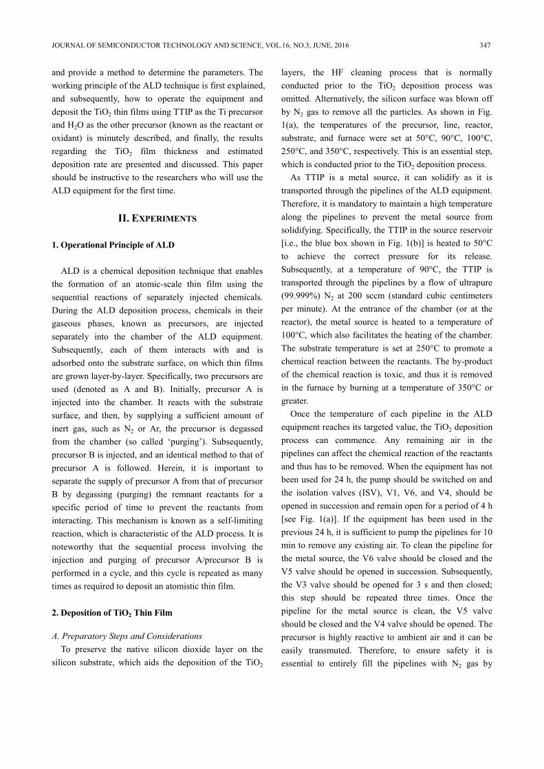
layers, the HF cleaning process that is normally conducted prior to the TiO2 deposition process was omitted. Alternatively, the silicon surface was blown off by N2 gas to remove all the particles. As shown in Fig. 1(a), the temperatures of the precursor, line, reactor, substrate, and furnace were set at 50°C, 90°C, 100°C, 250°C, and 350°C, respectively. This is an essential step, which is conducted prior to the TiO2 deposition process.
As TTIP is a metal source, it can solidify as it is transported through the pipelines of the ALD equipment. Therefore, it is mandatory to maintain a high temperature along the pipelines to prevent the metal source from solidifying. Specifically, the TTIP in the source reservoir [i.e., the blue box shown in Fig. 1(b)] is heated to 50°C to achieve the correct pressure for its release. Subsequently, at a temperature of 90°C, the TTIP is transported through the pipelines by a flow of ultrapure (99.999%) N2 at 200 sccm (standard cubic centimeters per minute). At the entrance of the chamber (or at the reactor), the metal source is heated to a temperature of 100°C, which also facilitates the heating of the chamber. The substrate temperature is set at 250°C to promote a chemical reaction between the reactants. The by-product of the chemical reaction is toxic, and thus it is removed in the furnace by burning at a temperature of 350°C or greater.
Once the temperature of each pipeline in the ALD equipment reaches its targeted value, the TiO2 deposition process can commence. Any remaining air in the pipelines can affect the chemical reaction of the reactants and thus has to be removed. When the equipment has not been used for 24 h, the pump should be switched on and the isolation valves (ISV), V1, V6, and V4, should be opened in succession and remain open for a period of 4 h [see Fig. 1(a)]. If the equipment has been used in the previous 24 h, it is sufficient to pump the pipelines for 10 min to remove any existing air. To clean the pipeline for the metal source, the V6 valve should be closed and the V5 valve should be opened in succession. Subsequently, the V3 valve should be opened for 3 s and then closed; this step should be repeated three times. Once the pipeline for the metal source is clean, the V5 valve should be closed and the V4 valve should be opened. The precursor is highly reactive to ambient air and it can be easily transmuted. Therefore, to ensure safety it is essential to entirely fill the pipelines with N2 gas by
348 KARAM CHO et al : ATOMIC LAYER DEPOSITION OF TIO2 USING TITANIUM ISOPROPOXIDE AND H2O: OPERATIONAL …
setting the N2 flow rate at 200 sccm for at least 1 min. When all the pipelines are filled with N2 gas, the out-manual valve of the TTIP source reservoir [shown in Fig. 1(c)] can be opened, and then the V6 and V5 valves should be closed and opened, respectively. Subsequently, the V3 valve should be opened for 3 s and then closed; this step should be repeated three times. Finally, by opening the manual valve of the H2O reservoir [shown in Fig. 1(b)], a sample can be loaded into the chamber of the ALD equipment.
To vent the chamber and load a sample, the V1 valve
should be open and all the other valves should be closed. It is necessary to feed N2 gas through the pipeline at 200 sccm and ensure that the pressure in the chamber is the same as the ambient air pressure (i.e., ~8.7E+2 Torr). The chamber can then be opened for a sample to be loaded. When a sample is loaded into the chamber, it is necessary to close/degas the chamber again by opening the ISV valve. While ensuring that the chamber pressure is decreasing, the flow rates for the N2 and precursor should be set as 200 and 40 sccm, respectively. Subsequently, the V6 and V4 valves should be opened in succession.
(a) (b)
(c)
Fig. 1. (a) Schematic illustrating the configuration of valves (V1 to V6 and ISV) along the pipelines and the temperature settings for the precursor, line, reactor, substrate, and furnace, (b) The reservoirs of H2O and TTIP are shown by the red and blue boxes, respectively, (c) in/out-manual valves of the TTIP source reservoir.

JOURNAL OF SEMICONDUCTOR TECHNOLOGY AND SCIENCE, VOL.16, NO.3, JUNE, 2016 349
Finally, to commence the TiO2 deposition process, it is essential to open the in-manual valve [shown in Fig. 1(c)].
B. TiO2 Deposition Process
A recipe, which is a series of settings used to not only control the number of cycles and elapse times for purging and source injection but also automatically manage the open and shut of the valves and the flow rate of purging gas during the deposition, is required to deposit TiO2 films using ALD.
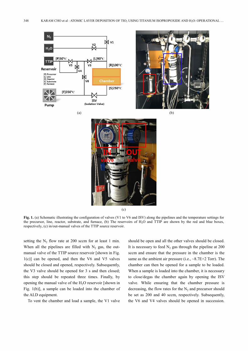
Using an in-house recipe, the TiO2 deposition process is controlled with five steps. As shown in Fig. 2(a), during step 1 the pipeline is purged for 60 s prior (V1, V4, V5 and ISV valves are designed to be open at each corresponding moment) to the deposition process to remove any remaining air. Subsequently, during step 2, the TiO2 films are deposited by repeating as many N cycles as required and by injecting the TTIP and H2O separately [Fig. 2(b)]. One cycle is organized by several stages; the pipeline is purged for 18 s to remove any remaining H2O from the previous cycle by keeping the condition of the valves at step 1, even though it is the first cycle to deposit the TiO2. Subsequently, V4 and V6
should be closed for 1.5 s, then the chamber is exposed to the TTIP for 0.1 s (V3 and V5 are designed to be open at this moment) for the titanium atoms to bond onto the surface of the substrate. To shut off the flow of TTIP precursor, V3 valve should be closed, and V4 valve should be opened for 1 s. Then, V5 should be closed, and V6 should be opened for the pipeline to be purged for 18 s in order to expel the by-products. Subsequently, an oxidant, H2O, is injected into the chamber for 0.2 s (V2 is designed to be open at this moment) and oxide radicals are formed on the substrate surface as a result of the chemical reaction between the TTIP and H2O. It is noteworthy to keep in mind two considerations: (1) V1 and ISV valves are always open in step 2, and (2) both reactants (i.e., TTIP and H2O in gas phases) are transported by the flow of ultrapure (99.999%) N2 gas during the deposition process. By repeating N cycles, the deposition of the TiO2 films is complete at the end.
The remaining steps (i.e., steps 3 to 5) are performed to remove the remnants of the reactants and by-products. During step 3, the pipelines are purged with a flow of N2 gas at 200 sccm for 60 s, while the V1, V4, V6, and ISV valves are open. This is followed by step 4, during which an N2 gas flow at 100 sccm is used and only the V1 and ISV valves are open. In step 5, the flow rate of the carrier gas is set to 0 sccm, and the V1 and ISV remain open. Hereby, the TiO2 deposition is complete.
C. Post-Treatment
To load out the TiO2-deposited sample from the chamber, the ISV valve should be closed and only the V1 valve should be open. The pipeline is filled by a flow of N2 gas at 200 sccm up to a chamber pressure of ~8.7E+2 Torr. Once the pressure reaches a sufficient value, the N2 flow rate is reduced to 40 sccm and the chamber is opened. The sample can then be removed and the chamber can be closed. Subsequently, the ISV valve should be opened and the manual valves associated with the precursor and H2O should be closed. Subsequently, all the temperatures associated with the system are set to 0°C, and when all the parts are chilled, the MFC parameters can be set to zero. Finally, to shut down the ALD equipment, all the valves should be closed and the pump can then be switched off.
(a)
(b)
Fig. 2. Schematic illustrating (a) the organization of the entire deposition sequence, (b) a detailed flow chart of a single cycle at step 2.

350 KARAM CHO et al : ATOMIC LAYER DEPOSITION OF TIO2 USING TITANIUM ISOPROPOXIDE AND H2O: OPERATIONAL …
III. RESULTS AND DISCUSSION
It is noteworthy that the thickness of the thin film is proportional to the number of cycles. Specifically, the linearity of the recipe is significantly important; this property is used to determine the number of cycles required to achieve the desired film thickness. We performed thin film deposition with various numbers of cycles (i.e., from sub-100 cycles to 800 cycles) to confirm the linearity of the newly developed recipe. The thickness of the TiO2 film was measured by spectroscopic ellipsometry, and its deposition rate was estimated [see Fig. 3(a) and (b)]. As shown in Fig. 3(a), the thickness of the TiO2 film linearly increases with the number of cycles. Note that, under the 200 cycles, the thickness of the TiO2 is in the degree of sub-10 nm, which is appropriate for
sub-10 nm CMOS technology node. With the in-house recipe, the deposition rate is
estimated to be 0.49 Å/cycle. We consider that such a low deposition rate results from the short injection time of 0.1 s. However, this value can be modified by controlling the parameters, such as the temperature settings, especially the substrate temperature, and the period of time specified for the source (TTIP) injection [10]. Also, temperatures of precursor, line and reactor might be able to affect the deposition rate because the velocity of the gaseous TTIP precursor source and its flow into the chamber can be affected. Therefore, by utilizing the in-house recipe, adequate recipe can be made for any researchers using ALD equipment.
IV. CONCLUSION
The deposition of a TiO2 thin film by the ALD process, using TTIP and H2O as precursors, was described in great detail. The thickness of the TiO2 film was controlled by varying the number of cycles and its deposition rate was estimated to be 0.49 Å/cycle. In this work, the method of operation for the ALD equipment, as well as the settings for the associated parameters, was depicted in detail. It is recommended that the parameters, such as the temperatures, purging times, and precursor injection times are optimized to guarantee the linearity of the thin film growth, on the scale of a few nanometers, with the number of cycles.
REFERENCES
[1] Kemell, M., Pore, V., Tupala, J., Ritala, M., Leskelä, M., "Atomic layer deposition of nanostructured TiO2 photocatalysts via template approach", Chemistry of Materials, Vol.19, No.7, pp.1816-20, 2007.
[2] Euvananont, C., Junin, C., Inpor, K., Limthongkul, P., Thanachayanont, C., "TiO2 optical coating layers for self-cleaning applications", Ceramics International, Vol.34, No.4, pp.1067-71, 2008.
[3] Wang, C.-W., Chen, S.-F., Chen, G.-T., "Gamma-ray-irradiation effects on the leakage current and reliability of sputtered TiO2 gate oxide in metal-oxide-semiconductor capacitors", J. Appl. Phys., Vol.91, pp.9198-203, 2002.
(a)
(b)
Fig. 3. (a) TiO2 film thickness versus number of cycles, (b) estimated deposition rate versus number of cycles. Note that the average deposition rate is 0.49 Å/cycle.

JOURNAL OF SEMICONDUCTOR TECHNOLOGY AND SCIENCE, VOL.16, NO.3, JUNE, 2016 351
[4] Fröhlich, K., Ťapajna, M., Rosová, A., Dobročka, E., Hušeková, K., Aarik, J., et al., "Growth of high-dielectric-constant TiO2 films in capacitors with RuO2 electrodes", Electrochemical and Solid-State Letters, Vol.11, No.6, pp.G19-G21, 2008.
[5] Wu, T., Wu, C., Chen, M., "Highly insulative barium zirconate-titanate thin films prepared by rf magnetron sputtering for dynamic random access memory applications", Appl. Phys. Lett., Vol.69, No.18, pp.2659-61, 1996.
[6] Kim, K., Lee, S., "Integration of lead zirconium titanate thin films for high density ferroelectric random access memory", J. Appl. Phys., Vol.100, No.5, pp.051604, 2006.
[7] Aarik, L., Arroval, T., Rammula, R., Mändar, H., Sammelselg, V., Aarik, J., "Atomic layer deposition of TiO 2 from TiCl 4 and O 3", Thin Solid Films, Vol.542, pp.100-7, 2013.
[8] Elam, J., Schuisky, M., Ferguson, J., George, S., "Surface chemistry and film growth during TiN atomic layer deposition using TDMAT and NH 3", Thin Solid Films, Vol.436, No.2, pp.145-56, 2003.
[9] Ritala, M., Leskela, M., Niinisto, L., Haussalo, P., "Titanium isopropoxide as a precursor in atomic layer epitaxy of titanium dioxide thin films", Chemistry of materials, Vol.5, No.8, pp.1174-81, 1993.
[10] Xie, Q., Jiang, Y.-L., Detavernier, C., Deduytsche, D., Van Meirhaeghe, R. L., Ru, G.-P., et al., "Atomic layer deposition of TiO2 from tetrakis-dimethyl-amido titanium or Ti isopropoxide precursors and H2O", J. Appl. Phys., Vol.102, No.8, pp.083521, 2007.
Karam Cho received the B.S. degree in department of physics from University of Seoul, Seoul, Korea, in 2015 and she is currently working toward the M.S. degree in electrical and computer engineering from University of Seoul. Her research
interests include steep-switching CMOS emerging devices.
Jung-Dong Park received the B.S. degree from Dongguk University, Seoul, Korea, in 1998, the M.S. degree in Gwangju Institute of Science and Technology (GIST), Gwangju, Korea, in 2000, and the Ph.D. degree in EECS from the
University of California at Berkeley, in 2012. His research include device physics and modeling, analog, RF, mixed-signal, mm-wave integrated circuits, and microwave electronics including antennas.
Changhwan Shin received the B.S. degree (top honors) in Electrical Engineering from Korea University, Seoul, Korea, in 2006 and the Ph.D. degree in Electrical Engineering and Computer Sciences from the Univer- sity of California, Berkeley, in 2011.
In 2011, he joined the Silicon Technology Group, Xilinx Inc., San Jose, CA, as a Senior Process/Device Engineer. In 2012, he joined the Faculty of the University of Seoul, Seoul, Korea. His current research interests include advanced CMOS device designs and their applications to variation-robust SoC memory and logic devices, as well as CMOS extension technology and post-silicon technology. Prof. Shin was the recipient of a fellowship from the Korea Foundation for Advanced Studies (KFAS) in 2004, the General Electric Foundation Scholar Leaders Award in 2005, the Best Paper Award and the Best Student Paper Award at the IEEE International SOI Conference in 2009, and the Best Paper Award at the European Solid State Device Research Conference (ESSDERC) in 2010. He has been serving on technical committees for the IEEE International SOI conference (now, IEEE S3S conference) and the European Solid State Device Research Conference (ESSDERC).