atom optics for bose-einstein condensates (bec) · afrl-rv-ps- afrl-rv-ps- tr-2012-0104...
TRANSCRIPT
AFRL-RV-PS- AFRL-RV-PS- TR-2012-0104 TR-2012-0104 ATOM OPTICS FOR BOSE-EINSTEIN CONDENSATES (BEC) Steven Miller, et al. 25 April 2012 Final Report APPROVED FOR PUBLIC RELEASE; DISTRIBUTION IS UNLIMITED.
AIR FORCE RESEARCH LABORATORY Space Vehicles Directorate 3550 Aberdeen Ave SE AIR FORCE MATERIEL COMMAND KIRTLAND AIR FORCE BASE, NM 87117-5776
Approved for public release; distribution is unlimited.
DTIC COPY
NOTICE AND SIGNATURE PAGE
Using Government drawings, specifications, or other data included in this document for any purpose other than Government procurement does not in any way obligate the U.S. Government. The fact that the Government formulated or supplied the drawings, specifications, or other data does not license the holder or any other person or corporation; or convey any rights or permission to manufacture, use, or sell any patented invention that may relate to them.
This report was cleared for public release by the Air Force Research Laboratory 377 ABW Public Affairs Office and is available to the general public, including foreign nationals. Copies may be obtained from the Defense Technical Information Center (DTIC) (http://www.dtic.mil). AFRL-RV-PS-TR-2012-0104 HAS BEEN REVIEWED AND IS APPROVED FOR PUBLICATION IN ACCORDANCE WITH ASSIGNED DISTRIBUTION STATEMENT. //signed// //signed// ________________________________________ _______________________________________ Steven M. Miller Joel B. Mozer Project Manager, AFRL/RVBYE Chief, AFRL/RVB
This report is published in the interest of scientific and technical information exchange, and its publication does not constitute the Government’s approval or disapproval of its ideas or findings.

REPORT DOCUMENTATION PAGE Form Approved
OMB No. 0704-0188 Public reporting burden for this collection of information is estimated to average 1 hour per response, including the time for reviewing instructions, searching existing data sources, gathering and maintaining the data needed, and completing and reviewing this collection of information. Send comments regarding this burden estimate or any other aspect of this collection of information, including suggestions for reducing this burden to Department of Defense, Washington Headquarters Services, Directorate for Information Operations and Reports (0704-0188), 1215 Jefferson Davis Highway, Suite 1204, Arlington, VA 22202-4302. Respondents should be aware that notwithstanding any other provision of law, no person shall be subject to any penalty for failing to comply with a collection of information if it does not display a currently valid OMB control number. PLEASE DO NOT RETURN YOUR FORM TO THE ABOVE ADDRESS.
1. REPORT DATE (DD-MM-YYYY) 25-04-2012
2. REPORT TYPE Final Report
3. DATES COVERED (From - To) 29 Apr 03 – 15 Mar 12
4. TITLE AND SUBTITLE
5a. CONTRACT NUMBER
Atom Optics for Bose-Einstein Condensates (BEC) 5b. GRANT NUMBER
5c. PROGRAM ELEMENT NUMBER 61102F
6. AUTHOR(S) Matthew B. Squires, James A. Stickney, James Scoville, Paul M. Baker, Evan J. Carlson,
5d. PROJECT NUMBER 2301
Walter R. Buchwald, Sandra Wentzell, and Steven Miller
5e. TASK NUMBER PPM00004915
5f. WORK UNIT NUMBER EF004366
7. PERFORMING ORGANIZATION NAME(S) AND ADDRESS(ES) Air Force Research Laboratory Space Vehicles Directorate 3550 Aberdeen Ave SE Kirtland AFB, NM 87117-5776
8. PERFORMING ORGANIZATION REPORT NUMBER AFRL-RV-PS-TR-2012-0104
9. SPONSORING / MONITORING AGENCY NAME(S) AND ADDRESS(ES)
10. SPONSOR/MONITOR’S ACRONYM(S) AFRL/RVBYE
11. SPONSOR/MONITOR’S REPORT NUMBER(S)
12. DISTRIBUTION / AVAILABILITY STATEMENT Approved for public release; distribution is unlimited. (377ABW-2012-0624 dtd 21 May 12) 13. SUPPLEMENTARY NOTES 14. ABSTRACT During 2005, a new basic research effort was begun to better understand confined cold atom systems and determine if atom interferometry for the detection of rotation was possible utilizing spatially and temporally modulated magnetic fields generated using currents running through traces on microchips. During the next seven years, significant progress has been made in evaluating the constraints posed by both theory and practical experimental considerations. This report encompasses three of these studies: collisional decoherence in trapped interferometers, adjustable microchip ring-traps, and atom chips on direct bonded copper substrates. The first of these describes an analytical model developed to describe the effects of collisions between atoms in a harmonic magnetically confined atom interferometer. The second describes a method to create an agile circular magnetic waveguide for deBroglie waves on a microchip, while the third presents the use of direct bonded copper (DBC) for the straightforward fabrication of high power atom chips. Each of these efforts has incrementally added to our cold atom interferometry knowledge base and has enabled the future construction of a working atom chip based interferometer for the ultrasensitive detection of rotation. 15. SUBJECT TERMS Interferometer, cold atom, laser cooling, gyroscope, BEC, microchip, ring trap, atom chips, direct bonded copper, precision navigation
16. SECURITY CLASSIFICATION OF:
17. LIMITATION OF ABSTRACT
18. NUMBER OF PAGES
19a. NAME OF RESPONSIBLE PERSON Steven Miller
a. REPORT UNCLASSIFIED
b. ABSTRACT UNCLASSIFIED
c. THIS PAGE UNCLASSIFIED
UNLIMITED
52
19b. TELEPHONE NUMBER
Standard Form 298 (Rev. 8-98) Prescribed by ANSI Std. Z39.18

This page is intentionally left blank.
Approved for public release; distribution is unlimited.

i Approved for public release; distribution is unlimited.
Table of Contents
1. COLLISIONAL DECOHERENCE IN TRAPPED ATOM INTERFEROMETERS THAT USE NON-DEGNERATE SOURCES ..............................................................................................1
1.1 Introduction ............................................................................................................................1 1.2 Formulation of the Problem ...................................................................................................4 1.3 Discussion ..............................................................................................................................11 1.4 Conclusions ............................................................................................................................16
2. ADJUSTABLE MICROCHIP RING TRAP FOR COLD ATOMS AND MOLECULES ........16
2.1 Introduction ............................................................................................................................16 2.2 The 7-Wire Microchip Ring Trap Design ..............................................................................17 2.3 Theoretical Development .......................................................................................................18 2.4 Switching Between the 3-Wire and 4-Wire Ring Trap ..........................................................21 2.5 Conclusions ............................................................................................................................24
3. ATOM CHIPS ON DIRECT BONDED COPPER SUBSTRATES ..........................................25
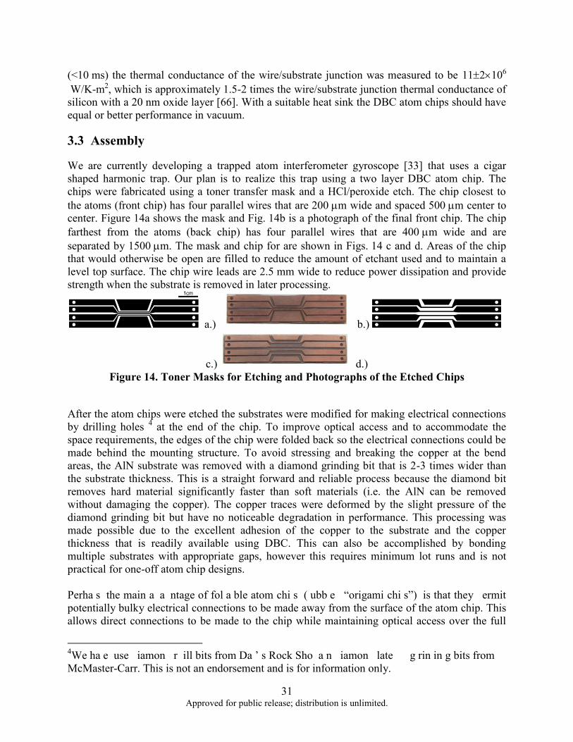
3.1 Introduction ............................................................................................................................25 3.2 Fabrication of Atom Chips Using Direct Bonded Copper .....................................................26 3.3 Assembly................................................................................................................................31 3.4 Conclusion .............................................................................................................................32
REFERENCES ............................................................................................................................34
APPENDIX: OPTIMAL WIRE ASPECT RATIO......................................................................40
LIST OF ACRONYMS ...............................................................................................................44

ii Approved for public release; distribution is unlimited.
List of Figures
1. A Schematic of the Interferometer Cycle ...................................................................................3 2. The Interference Signal as a Function of Time Near One Trap Period ....................................12 3. The Maximum Value of the Interference Signal as a Function of the Perpendicular Trapping Frequency .......................................................................................................................................13 4. The Maximum Value of the Interference Signal as a Function of Temperature ......................14 5. The Maximum Value of the Interference Signal as a Function of Number of Atoms in the Trap ................................................................................................................................................15 6. 7-Wire Ringtrap Layout Including the Appropriate Current Labels ........................................18 7. Trapping Potential in Gauss Along r-Axis for t=01 in Equal Steps .....................................22 8. Trapping Potential Below the Wires is Given in Gauss Along z-Axis for t=01 in Equal Steps ...............................................................................................................................................22 9. Maintaining a Constant Waveguide Minimum During the Transfer from 3-Wire to 4-Wire Waveguide is Represented by the Uniform Flatness of the Potential in the Switching Areas ......23 10. A Scanning Electron Micrograph of the Top View of Test Chip A .......................................29 11. A Scanning Electron Micrograph of the Cross Sectional View of Test Chip A .....................29 12. A Scanning Electron Micrograph of the Top View of Test Chip B .......................................30 13. A Scanning Electron Micrograph of the Cross Sectional View of Test Chip B .....................30 14. Toner Masks for Etching and Photographs of the Etched Chips ............................................31 15. Photograph of the DBC Atom Chip Assembly on Copper Mounting Post ............................32 A-1. The Optimal Aspect Ratio as a Function of the Ratio of Trap Height to Wire Thickness ......................................................................................................................................................41 A-2. The Maximum Value of the Dimensionless Magnetic Field Gradient as a Function of the Ratio of Trap Height to Wire Thickness .....................................................................................42
1 Approved for public release; distribution is unlimited.
1 COLLISIONAL DECOHERENCE IN TRAPPED ATOM
INTERFEROMETERS THAT USE NON-DEGENERATE SOURCES
1.1 Introduction
To date cold atom interferometers have demonstrated rotation sensitivities comparable to ring laser and mechanical gyroscopes [1]. Several atom interferometer schemes have been realized, and thus far free space fountain and beam configurations, that utilize light pulses to manipulate the atoms, have demonstrated the greatest sensitivities [1, 2, 3]. While the lack of external potential reduces systematic errors, atom interferometry in free space is limited by acceleration due to gravity. In particular, the precision of an interferometer is directly proportional to the interrogation time and in free space this time is limited by the size of the vacuum chamber. In the most sensitive free space atom interferometers, the atomic clouds travel up to 10 meters [2]. The large scale of free space interferometers limits their applications. There is currently a great effort being made to reduce the size of atom interferometers while simultaneously increasing their sensitivity. One straightforward way to achieve this goal is to develop interferometers that trap the atoms in an external potential for the duration of the interferometer cycle. The external potential prevents the atoms from falling due to gravity, and keeps the atomic gas from expanding in the vacuum chamber. As a result, the interferometer cycle time is not as limited by the size of the chamber.
Several groups have built trapped atom interferometers using atomic gases that are both above and below the recoil temperature [4, 5, 6, 7, 8, 9]. To date, all interferometers that use gases below the recoil temperature have utilized atoms in a nearly pure Bose-Einstein condensate (BEC). If the gas is cooled below the recoil temperature and is split using a laser pulse, a large relative separation between each arm of the interferometer can be achieved [6]. By exposing the atoms in each arm to a different environment, precision measurements of localized phenomena can be performed. For example, the AC stark shift in 87Rb was recently measured by exposing the atoms in one arm of an interferometer to laser light [10]. In some applications, such as the sensing of rotations and accelerations, cloud separation is not necessary and interferometers that use non-degenerate source are sufficient. These sources can be produced by laser cooling alone. Additionally, non-degenerate atomic gases have a much lower density compared to a BEC and therefore experience a weaker mean-field potential. The mean-field potential directly couples number uncertainty into phase uncertainty via number dependent phase diffusion [8, 11, 12, 13]. One advantage of working with laser cooled gases is that dephasing due to number fluctuations is ameliorated. Besides the elimination of mean-field effects, atom interferometers that use laser cooled atomic gases are less sensitive to heating due to imperfections in the confining potential than a BEC. Atoms in a pure BEC experience no momentum changing collisions with other atoms in the same mode. Therefore, an interferometer that uses a pure BEC will experience little decoherence

2 Approved for public release; distribution is unlimited.
due to collisions. However, if a BEC is heated, atoms will leave the condensate and will experience an increase in the collision frequency. As a result, the decoherence rate will increase with temperature. On the other hand, if the interferometer uses a laser cooled gas with a temperature much greater than the BEC transition temperature, the density will decrease as the temperature increases and the decoherence rate will decrease if the gas is inadvertently heated. Several different methods for building atom interferometers using laser cooled gases have been developed [14] and time-domain atom interferometers that use a single internal quantum state [15] lend themselves naturally for use with trapped atomic gases. This type of interferometer uses a series of optical standing waves to manipulate the external states of the atoms in the cloud. The interferometric cycle begins by loading an atomic cloud in a magneto-optical trap. The trap is switched off and the atomic cloud begins to fall due to gravity. At the time t=0, the cloud is illuminated with a short pulse from the standing wave laser field. Shortly after the pulse, the cloud has a density modulation with a period of /2, where is the wavelength of the laser field. The density modulation then disappears because of the thermal motion of the atoms in the cloud. At the time t=T the gas is illuminated with a second pulse. Due to the Talbot-Lau effect, there is an echo of the density modulation at the times t=nT, for integers n2. If the atomic cloud experiences a non-uniform potential during the interferometer cycle, the density echoes will be shifted relative to the initial modulation. The shift in the phase of the modulation can be determined by reflecting a probe pulse from a single laser beam off of the echo. The phase of the reflected probe pulse is directly proportional to the phase shift in the density modulation. By interfering the reflected probe pulse with a reference beam, the interferometer’s signal can be read. Recently, a trapped time domain atom interferometer was built by the group at Harvard [9]. This interferometer used an atom wave guide to confine the atoms in the perpendicular directions while allowing them to freely propagate along the parallel direction. A series of standing wave laser pulses were applied to the atoms, such that the wave vectors of the lasers pointed along the free direction of the guide. The Harvard group demonstrated that it is possible to electronically move the wave guide back and forth perpendicular to the free direction of the wave guide so that the arms of the interferometer enclose an area, making the interferometer sensitive to rotations [9]. A major difficulty with all trapped atom interferometers that use optical pulses is that the residual potential along the guide causes decoherence [16, 17, 18, 19]. The groups that have built BEC based interferometers have mitigated the decoherence by either using a double reflection geometry or using the classical turning points of the residual potential to reflect the atoms. The Harvard group has reduced the effects of the residual potential by using interferometric cycles with several laser pulses [20]. Although this multi-pulse scheme greatly increases the coherence time of the interferometer, it also reduces the number of atoms participating as well as reducing the area enclosed by the interferometer.
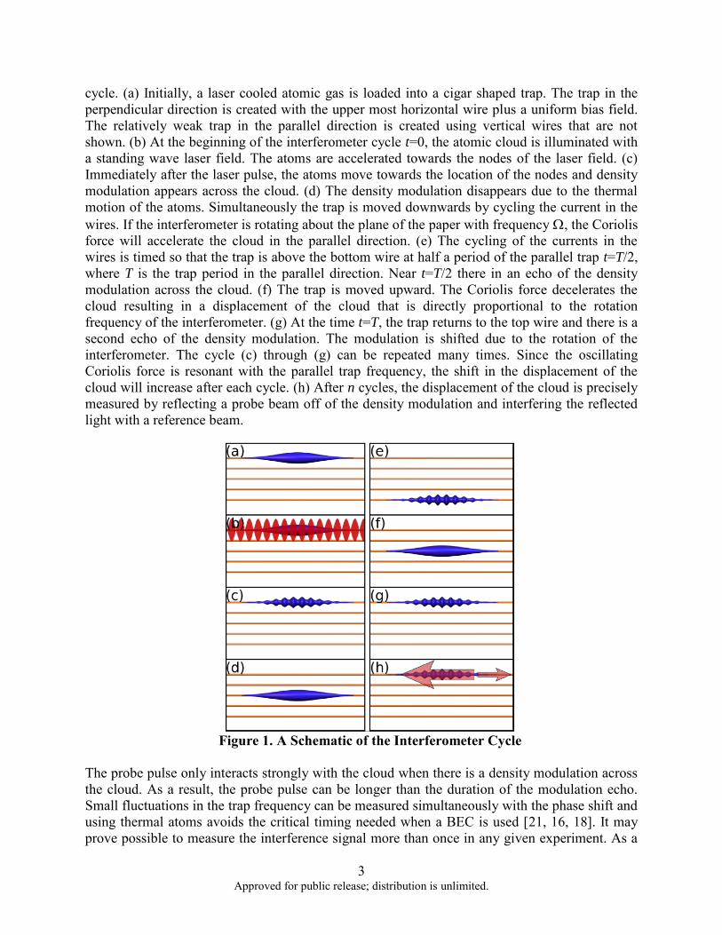
We are currently developing a trapped atom gyroscope that uses a laser cooled atomic gas and avoids decoherence due to the residual potential by using classical turning points to reflect the atoms. Rather than utilizing the Talbot-Lau effect, the density modulation will echo twice every oscillation of the atoms in the parallel direction. Figure 1 is a schematic of the interferometer
3 Approved for public release; distribution is unlimited.
cycle. (a) Initially, a laser cooled atomic gas is loaded into a cigar shaped trap. The trap in the perpendicular direction is created with the upper most horizontal wire plus a uniform bias field. The relatively weak trap in the parallel direction is created using vertical wires that are not shown. (b) At the beginning of the interferometer cycle t=0, the atomic cloud is illuminated with a standing wave laser field. The atoms are accelerated towards the nodes of the laser field. (c) Immediately after the laser pulse, the atoms move towards the location of the nodes and density modulation appears across the cloud. (d) The density modulation disappears due to the thermal motion of the atoms. Simultaneously the trap is moved downwards by cycling the current in the wires. If the interferometer is rotating about the plane of the paper with frequency , the Coriolis force will accelerate the cloud in the parallel direction. (e) The cycling of the currents in the wires is timed so that the trap is above the bottom wire at half a period of the parallel trap t=T/2, where T is the trap period in the parallel direction. Near t=T/2 there in an echo of the density modulation across the cloud. (f) The trap is moved upward. The Coriolis force decelerates the cloud resulting in a displacement of the cloud that is directly proportional to the rotation frequency of the interferometer. (g) At the time t=T, the trap returns to the top wire and there is a second echo of the density modulation. The modulation is shifted due to the rotation of the interferometer. The cycle (c) through (g) can be repeated many times. Since the oscillating Coriolis force is resonant with the parallel trap frequency, the shift in the displacement of the cloud will increase after each cycle. (h) After n cycles, the displacement of the cloud is precisely measured by reflecting a probe beam off of the density modulation and interfering the reflected light with a reference beam.
Figure 1. A Schematic of the Interferometer Cycle
The probe pulse only interacts strongly with the cloud when there is a density modulation across the cloud. As a result, the probe pulse can be longer than the duration of the modulation echo. Small fluctuations in the trap frequency can be measured simultaneously with the phase shift and using thermal atoms avoids the critical timing needed when a BEC is used [21, 16, 18]. It may prove possible to measure the interference signal more than once in any given experiment. As a
4 Approved for public release; distribution is unlimited.
result, it might be possible to split the atoms once, and measure the rotation frequency several times as the cloud oscillates in the trap. During interferometer cycle, collisions between the trapped atoms will bring the gas back to equilibrium, causing a reduction in the amplitude of the density modulation. Thus, the amplitude of the reflected probe pulse will degrade with time. The upper limit on the interferometer cycle time and the devices sensitivity can be determined by analyzing the effects collisions between the atoms in the trap. In this chapter, we present a theoretical model for our interferometer. In Sec. 1.2, we present an analytic model for the amplitude of the reflected probe pulse including the rotation of the interferometer and the effects of collisions between the atoms in the gas. In Sec. 1.3 the analytic model will be used to estimate the minimum value of the trap frequency in the perpendicular direction, the optimal temperature of the gas, and the optimal number of atoms to use in our upcoming experiment and we compare the results of our analytic model with a Direct simulation Monte-Carlo code. Finally Sec. 1.4 conclusions will be presented.
1.2 Formulation of the Problem
The dynamics of a dilute atomic gas above BEC phase transition temperature is governed by the quantum Boltzmann equation [22]
(1) where is the single particle density operator, H
eff is the effective single particle Hamiltonian,
and I() is the collision integral. The effective Hamiltonian for an atom in a rotating trap and standing wave laser field is
(2) where m is the atomic mass, V is the external trapping potential, characterizes the strength of the standing wave laser, k
l is the wave vector of the laser field, and is the vector that points
along the axes of rotation with the magnitude of the angular rotation frequency. The final term in Eq. (2) is the mean-field potential where U0=42a
s/m characterizes strength of the atom-atom
interactions, as is the s-wave scattering length, and n is the number density of the atomic gas.
Note that the mean field potential for a non-condensed gas is a factor of two larger than for a BEC with the same density. It is convenient to recast the single particle density operator in the Wigner function representation which is defined as

5 Approved for public release; distribution is unlimited.
(3) where |r are the eigenstates of the coordinate operator. The Wigner function can be interpreted as the probability density of finding an atom at the coordinate r with momentum p. It will be assumed that the standing wave laser pulse is in the Kapitza-Dirac regime. It is sufficiently short that both the free evolution of the gas and the collision integral may be neglected, i.e. the atoms do not move and experience no collisions while the laser beams are on. The pulse is in this regime when
(4) where
p is the length of the pulse, is the a e length of the laser beams, is the a e rage s e e
of the atoms in the gas, and is the average collision frequency. When Eq. (4) is fulfilled the dynamics of the atomic gas can be separated into two parts: the dynamics when the laser beams are on and the dynamics when the laser beams are off. In what follows the dimensionless coordinate r'=2k
lx, the dimensionless momentum p'=p/2k
l
and the dimensionless time t'=t/t0 where t0=m/4k2l will be used. For 87Rb, the characteristic time
is t0=5.3 s. Substituting Eq. (3) and (2) into Eq. (1) the dimensionless equation of motion for the Wigner function f, when the laser beams are on, is
(5) where k
l'=k
l/k
l is the direction of the standing wave laser field, '=t0 is the dimensionless laser
strength, and all of the primes have been dropped. Similarly, the dimensionless equation of motion for the Wigner function f, when the laser beams are off, is
(6) where '=t0, y0'=2k
ly0 and once again all the primes have been dropped. Our short term goal is
to measure the rotation of the Earth. For 87Rb the rotation frequency of the Earth in our dimensionless units is
E=41010. When the gas is in thermodynamic equilibrium, the

6 Approved for public release; distribution is unlimited.
dimensionless temperature is T'=T/4TR, where T
R=2k
2l /mk
B is the one photon recoil temperature.
For 87Rb, the recoil temperature is TR=350 nK.
The dimensionless effective potential is
(7) where V'=t0V/ is the dimensionless trapping potential, n'=8k
3l n is the dimensionless density, and
g=8ask
l is the dimensionless mean-field strength. For 87Rb the dimensionless mean-field
strength is g1. The length scale L of density changes in a magnetically trapped atomic gas is typically much larger than the atoms s-wave scattering length a
s, i.e. a
s/L˂˂1. In this limit, the collision integral
becomes independent of the potential. Since the atomic gas is above the BEC transition temperature, no single quantum state has a macroscopic population and Bose enhanced scattering can be neglected. The dimensionless collision integral can be approximated with the classical collision integral [22]
(8) where =32a
2sk
2l is the dimensionless collision cross section. For 87Rb the dimensionless
scattering cross section is =0.2. Before the laser pulse is applied, the gas is in thermodynamic equilibrium and it will be assumed that the laser pulse is sufficiently weak that the gas is always close to equilibrium. The Wigner function f can be written as
(9) where f0 is the equilibrium Wigner function and f is the disturbance caused by the laser pulse. When the disturbance is much smaller than the equilibrium | f |<<| f |, Eq. (8) can be approximated as [23]
(10)
Equation (10) is the sum of three terms, each with a simple physical interpretation. The first term
is proportional to the rate that an atom in f0 scatters with an atom in f and one of the atoms scatters into the momentum state p. The second term is proportional to the rate that atoms scatter out of f because of collisions with atoms in f0. The final term is the inverse of the second process.
7 Approved for public release; distribution is unlimited.
Only atoms in the disturbance contribute to the interference signal. Therefore, once an atom scatters out of the disturbance it no longer contributes to the interference signal. As a result, only the second term in Eq (10) contributes to the loss of the interference signal and the collision integral Eq. (10) becomes
(11) where the collision frequency is given by the integral
(12) Substituting the equilibrium distribution
(13) into Eq. (12), the collision frequency Eq. (12) becomes
(14) where
(15) The integral K() can be explicitly evaluated in terms of error functions. To remove the dependence of on the coordinate r and momentum p, Eq. (15) will be replaced by its value a zero argument K=1 and the density n will be replaced by the averaged density of a gas thermodynamic equilibrium in a harmonic potential. The collision frequency Eq. (12) becomes
(16) Where is the geometric average of the trap frequencies. In Sec. 1.3 it will be demonstrated that using Eq. (16) for the collision frequency yields accurate results when compared to a more complete description of the atomic collisions. For the rest of this paper, we will limit the discussion to the case of a cigar shaped harmonic potential. The dimensionless trapping potential becomes

8 Approved for public release; distribution is unlimited.
(17) where
'=t0
and ||'=t0||. If the trap has frequencies ||=23 Hz and =2300 Hz, the
dimensionless trap frequencies for 87Rb are ||'=104 and '=102.
When the gas is close to thermodynamic equilibrium in a harmonic trap the density is
(18) where N is the number of atoms in the trap and V is the potential. Using Eq. (7) and (18) the effective potential can be expanded to fourth order as
(19) The lowest order mean field contribution to the potential causes a small reduction of the trap frequency. Therefore, the oscillation period of atoms in the trap is weakly dependent on the number of trapped atoms. The next higher order contribution is a weak quartic contribution to the potential. This, and all higher order terms, can be neglected when
(20) For example if the trap contains 7106 87Rb atoms, in a trap with frequencies ||=23 Hz and =2300 Hz, and a temperature of 40 K (T=30), the left hand side of Eq. (20) is about 6x10-
8. In this case, the quantric contribution to the potential can be neglected. The analysis of the operation of the interferometer will be limited to the case where the splitting and read lasers beams are aligned with the weak axis of the harmonic potential, which will be chosen to be the x direction. For definiteness, the rotation of the interferometer will be in the z direction and the trap will be moved in the y direction. An atomic cloud at temperature T remains in equilibrium if the center of the trap is translated adiabatically. The trajectory of the moving trap y0(t) is adiabatic when
(21) where
is the trap frequency in the y direction.
When Eq. (21) is fulfilled, the equations of motion Eq. (5) and (6) can be recast in a one-dimensional form. The Wigner function is written as the product
9 Approved for public release; distribution is unlimited.
f(x,r,p,p
)=f(x,p)F(r
,p) , where F(r
,p) is the equilibrium distribution in the
perpendicular direction, normalized to one, and f(x,p) is the non-equilibrium distribution in the parallel direction, normalized to the number of atoms in the trap. When the laser beams are on, the one-dimensional equation of motion for the Wigner function is
(22) The solution of Eq. (22) can be written in terms of Bessel functions of the first kind J
,
(23) where the sum over k and l runs from to , = dt'(t') is the strength of the laser pulse, and
(24) is the equilibrium Wigner function at temperature T. In general Eq. (23) can be negative, because the resulting gas is in a non-classical state. However, for high temperatures T>>1 the negative parts of the Wigner function are negligible, and the gas may be treated classically. After the laser pulse is applied, the optical field is turned off and the one-dimensional equation of motion for the Wigner function becomes
(25) where the collision frequency is given by Eq. (16). The left hand side of Eq. (25) can be greatly simplified by introducing the new coordinates
(26) In this new coordinate system, Eq. (25) becomes

10 Approved for public release; distribution is unlimited.
(27) which has the general solution (28) where f(0) is the initial Wigner function given by Eq. (23), f0 is the equilibrium Wigner function given by Eq. (24), and is given by Eq. (16). To read out the accumulated phase, the atomic cloud is illuminated with a single off resonate laser beam. The light that is back scattered off of the cloud is mixed with a reference beam [15,17]. By measuring the interference intensity, the amplitude of the scattered light can be determined. Using the Born approximation, it can be shown that the amplitude of the back scattered light is proportional to [17]
(29) where f is the one-dimensional Wigner function. The quantity S will be referred to as the interference signal of the interferometer. In the new coordinate system Eq. (26), the signal becomes
(30) where
(31)
is the phase shift due to the rotation of the interferometer. Substituting Eq. (28) into Eq. (30) yields
(32)
The interference signal S is only nonzero when t2n/, where n is an integer or half integer. Expanding Eq. (32) near these points and taking the limit where T>>ω2 yields
(33)
11 Approved for public release; distribution is unlimited.
where =t2n/||. Equation (33) along with Eq. (16) and (31) are the main analytical results of this paper.
1.3 Discussion
Equation (33) will now be analyzed and optimal operating conditions for trapped thermal atom interferometers will be found. Additionally to confirm the results of the analytic model we will use a direct simulation Monte-Carlo model (DSMC) of the interferometer [24]. Direct simulation Monte-Carlo is accurate because the equation of motion after the laser pulse Eq. (6) is equivalent to the classical Boltzmann equation. Since the effect of the standing wave laser pulse on the cloud is non-classical (Eq. (22) ), DSMC can only be used to model the dynamics when the standing wave laser beams are off. To account for the laser pulse, the initial conditions for the DSMC model were set by Eq. (23). In regions where the initial Wigner function is negative f<0, the classical distribution of atoms was set to zero. This is valid when the temperature is much larger than the two-photon recoil temperature T>>1. For definitiveness, we specialize to the case where the trap is moved back and fourth according to
(34) where d is the dimensionless distance that the atomic cloud is displaced in the y-direction. Our chip will displace the trap about 5 mm, for 87Rb the dimensionless displacement will be d=8104. After n/2 oscillations, the atoms scattered into the first order will enclose an area nd/|| and the accumulated phase shift is
(35) To measure the rotation rate of the Earth, with a phase shift in a trap with ||=23 Hz, the trap must be moved back and forth three times. The time that it takes for the interferometer to measure a given phase shift does not depend on the parallel trap frequency. For example the time that it takes to measure a phase shift t
is
(36) To measure Earth’s rotation, ith a phase shift, the interferometer must have a cycle time of about one second. To measure a given rotation frequency, the bandwidth of the interferometer can only be increased by increasing the distance that the atoms are displaced d. For the
12 Approved for public release; distribution is unlimited.
remainder of this paper only the interference signal will be discussed for the case where the phase shift is zero and when the trap is not moved in the y-direction.
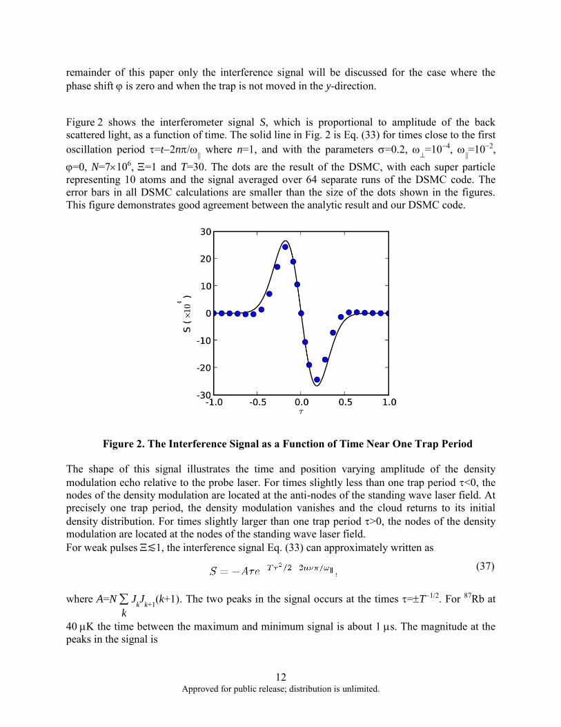
Figure 2 shows the interferometer signal S, which is proportional to amplitude of the back scattered light, as a function of time. The solid line in Fig. 2 is Eq. (33) for times close to the first oscillation period =t2n/|| where n=1, and with the parameters =0.2,
=104, ||=102,
=0, N=7106, =1 and T=30. The dots are the result of the DSMC, with each super particle representing 10 atoms and the signal averaged over 64 separate runs of the DSMC code. The error bars in all DSMC calculations are smaller than the size of the dots shown in the figures. This figure demonstrates good agreement between the analytic result and our DSMC code.
Figure 2. The Interference Signal as a Function of Time Near One Trap Period The shape of this signal illustrates the time and position varying amplitude of the density modulation echo relative to the probe laser. For times slightly less than one trap period <0, the nodes of the density modulation are located at the anti-nodes of the standing wave laser field. At precisely one trap period, the density modulation vanishes and the cloud returns to its initial density distribution. For times slightly larger than one trap period >0, the nodes of the density modulation are located at the nodes of the standing wave laser field. For weak pulses ≲1, the interference signal Eq. (33) can approximately written as
(37) where A=N
k
JkJ
k+1(k+1). The two peaks in the signal occurs at the times =T1/2. For 87Rb at
40 K the time between the maximum and minimum signal is about 1 s. The magnitude at the peaks in the signal is
13 Approved for public release; distribution is unlimited.
(38)
where Eq. (16) was used. For the remainder of this section, Eq. (38) will be analyzed for several illustrative cases. Using this analysis, limits on the performance of the interferometer will be discussed.
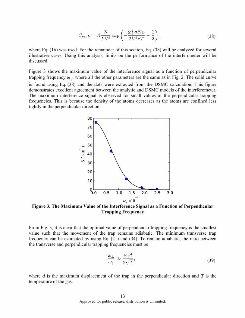
Figure 3 shows the maximum value of the interference signal as a function of perpendicular trapping frequency
, where all the other parameters are the same as in Fig. 2. The solid curve
is found using Eq. (38) and the dots were extracted from the DSMC calculation. This figure demonstrates excellent agreement between the analytic and DSMC models of the interferometer. The maximum interference signal is observed for small values of the perpendicular trapping frequencies. This is because the density of the atoms decreases as the atoms are confined less tightly in the perpendicular direction.
Figure 3. The Maximum Value of the Interference Signal as a Function of Perpendicular
Trapping Frequency
From Fig. 3, it is clear that the optimal value of perpendicular trapping frequency is the smallest value such that the movement of the trap remains adiabatic. The minimum transverse trap frequency can be estimated by using Eq. (21) and (34). To remain adiabatic, the ratio between the transverse and perpendicular trapping frequencies must be
(39)
where d is the maximum displacement of the trap in the perpendicular direction and T is the temperature of the gas.
14 Approved for public release; distribution is unlimited.
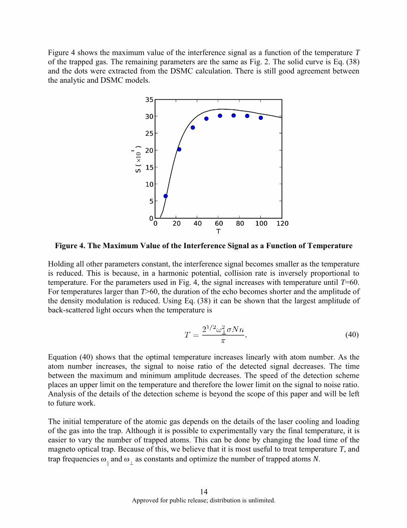
Figure 4 shows the maximum value of the interference signal as a function of the temperature T of the trapped gas. The remaining parameters are the same as Fig. 2. The solid curve is Eq. (38) and the dots were extracted from the DSMC calculation. There is still good agreement between the analytic and DSMC models.
Figure 4. The Maximum Value of the Interference Signal as a Function of Temperature
Holding all other parameters constant, the interference signal becomes smaller as the temperature is reduced. This is because, in a harmonic potential, collision rate is inversely proportional to temperature. For the parameters used in Fig. 4, the signal increases with temperature until T=60. For temperatures larger than T>60, the duration of the echo becomes shorter and the amplitude of the density modulation is reduced. Using Eq. (38) it can be shown that the largest amplitude of back-scattered light occurs when the temperature is
(40)
Equation (40) shows that the optimal temperature increases linearly with atom number. As the atom number increases, the signal to noise ratio of the detected signal decreases. The time between the maximum and minimum amplitude decreases. The speed of the detection scheme places an upper limit on the temperature and therefore the lower limit on the signal to noise ratio. Analysis of the details of the detection scheme is beyond the scope of this paper and will be left to future work. The initial temperature of the atomic gas depends on the details of the laser cooling and loading of the gas into the trap. Although it is possible to experimentally vary the final temperature, it is easier to vary the number of trapped atoms. This can be done by changing the load time of the magneto optical trap. Because of this, we believe that it is most useful to treat temperature T, and trap frequencies || and
as constants and optimize the number of trapped atoms N.
15 Approved for public release; distribution is unlimited.
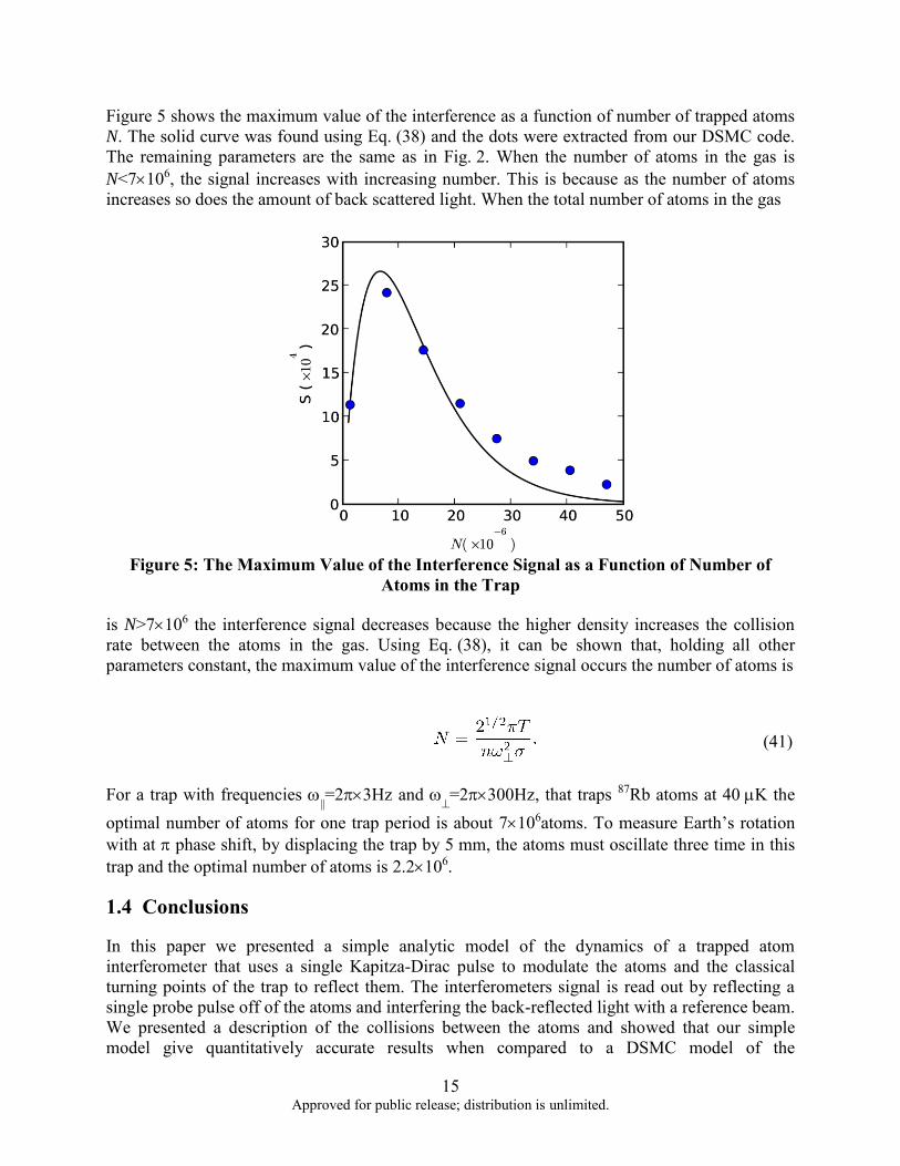
Figure 5 shows the maximum value of the interference as a function of number of trapped atoms N. The solid curve was found using Eq. (38) and the dots were extracted from our DSMC code. The remaining parameters are the same as in Fig. 2. When the number of atoms in the gas is N<7106, the signal increases with increasing number. This is because as the number of atoms increases so does the amount of back scattered light. When the total number of atoms in the gas
Figure 5: The Maximum Value of the Interference Signal as a Function of Number of
Atoms in the Trap
is N>7106 the interference signal decreases because the higher density increases the collision rate between the atoms in the gas. Using Eq. (38), it can be shown that, holding all other parameters constant, the maximum value of the interference signal occurs the number of atoms is
(41)
For a trap with frequencies ||=23Hz and
=2300Hz, that traps 87Rb atoms at 40 K the
optimal number of atoms for one trap period is about 7106atoms. To measure Earth’s rotation with at phase shift, by displacing the trap by 5 mm, the atoms must oscillate three time in this trap and the optimal number of atoms is 2.2106.
1.4 Conclusions
In this paper we presented a simple analytic model of the dynamics of a trapped atom interferometer that uses a single Kapitza-Dirac pulse to modulate the atoms and the classical turning points of the trap to reflect them. The interferometers signal is read out by reflecting a single probe pulse off of the atoms and interfering the back-reflected light with a reference beam. We presented a description of the collisions between the atoms and showed that our simple model give quantitatively accurate results when compared to a DSMC model of the
16 Approved for public release; distribution is unlimited.
interferometer. Finally, we used our model to find the optimal temperature or number to maximize the performance of the interferometer. Although the analytic model presented in this paper specialized to the analysis of a single Kapitza-Dirac pulse, the results of Sec. 1.3 easily generalize to multi-pulse interferometers [17,20]. To apply our model to interferometers that use gases above the BEC transition temperature but below the recoil temperature the momentum and spacial dependence on the collision frequency cannot be ignored and Eq. (12) must be used instead of Eq. (16). We believe that inclusion of the more complicated collision frequency will not dramatically change the results of this paper when describing a gas below the recoil temperature.
2 ADJUSTABLE MICROCHIP RING TRAP FOR COLD ATOMS AND
MOLECULES
2.1 Introduction
In recent years atom interferometry has been used to make precision measurements of various phenomena such as rotations, acceleration, gravity gradients and frequency separation of the hyperfine splitting for precision timekeeping [25, 26]. The sensitivity of these measurements are directly proportional to the interaction time or, in the case of rotation measurements, the area enclosed by the two separate interferometer paths. State of the art atom interferometers [25, 26, 27, 28, 29, 30] use unconfined launched atom clouds with minimal external potentials during the interferometer cycle. Despite the success of unconfined atom interferometers there are limitations on the ultimate sensitivity which include: gravity accelerating the atoms [31], increasing the enclosed area requires increasing the size of the required magnetic shielding, longer interaction times leads to lower signal to noise resulting from lower densities because of ballistic expansion of the atomic cloud, limited dynamic range due to the atom clouds impacting the rotating vacuum enclosure during high dynamic rotations. One method of addressing these difficulties is to place the atoms in a confining potential. Several methods for building potentials suitable for use in confined atom interferometers have been developed [27, 28, 29, 30, 32]. One method for producing a potential suitable for confined atom interferometry involves fabricating small micrometer scale current carrying wires on an insulating substrate, commonly referred to as an atom chip. Current carrying wires on atom chips produce magnetic fields that can be used to trap atomic samples when prepared in a low-field seeking state. However, to be effective for trapped atom interferometry, the magnetic potential must be sufficiently uniform to avoid decoherence. The requirements on the smoothness of the potential are reduced if the separate atomic clouds propagate through reciprocal paths, canceling common mode noise [27] and when the energy associated with the cloud is higher than the potential roughness [33]. Atom interferometry for rotation sensing via the Sagnac effect is one of the most promising applications of trapped atom interferometers. To maximize the enclosed area, and thus sensitivity, the atomic clouds used in the interferometer should propagate in a circle. In this paper, we propose a method for fabricating an atom chip ring trap, specifically for use in atom interferometry.
17 Approved for public release; distribution is unlimited.
A challenge of the ring traps using atom chips is the elimination of potential imperfections resulting from the input leads. One method of avoiding the input leads is to use several turns in an effort to make the input lead perturbation small in comparison to the ring field [34]. More recently magnetic induction has been proposed as means to avoid input leads [35]. In our previous paper [36] we proposed two sets of wires that provide two overlapping ring traps about a common radius and the ability to switch between the two in order to avoid the input leads. This method also provided a means of loading the atoms directly into the waveguide via a U-trap wire located adjacent to the ring to avoid atom losses [37]. An experimental limitation of this design was a fixed trapping height based upon the wire spacing and current ratios of the wires. Often the desired working distance is unknown and is not cost or time effective to redesign and replace chips often. For this reason a chip design with adjustable trapping distance is strongly desired. There are several reasons why a ring trap with an adjustable trapping height is experimentally useful. First, the lifetime of the atomic cloud trapped near the surface of an atom chip is limited by trap loss caused by Johnson noise photon induced spin flips [38]. The number of Johnson noise photons produced is dependent on the temperature of the chip, which depends upon the current density of the wires and the thermal properties of the microchip. Because producing the same magnetic confinement further from a wire requires more current and therefore a higher chip temperature, optimizing the distance of the atoms from the chip is experimentally important. Also, the atom interferometer requires some form of splitting and re-combining of the atoms. A common method used is to apply an optical standing wave. Once again the distance of the atoms from the microchip is important because the Bragg scattering efficiency is reduced by the scattering of the laser beams off the chip surface. Finally, increasing the distance from the waveguide to the chip surface also averages small imperfection in the potential resulting from current fluctuations in the wires. For all of these reasons it is desirable to have a chip design that allows for an adjustable trapping distance by changing the wire currents.
2.2 The 7-Wire Microchip Ring Trap Design
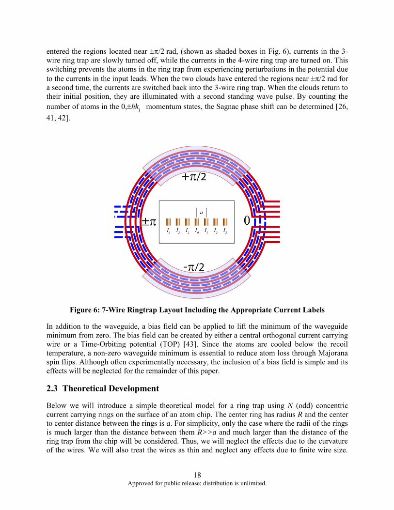
Previous work has shown that a waveguide with a magnetic field minimum can be generated utilizing either 3 or 4 straight current carrying wires [39, 40]. Specific currents in the wires can be chosen, so as to produce a trapping potential some distance away from the wires. In this paper it will be demonstrated that it is possible to use 7 concentric circular wires to produce a uniform ring trap waveguide that avoids perturbations resulting from the input leads. A schematic of our 7-wire ring trap is shown in Fig. 6. Since there are a total of seven concentric current rings used to form this ring trap, we will refer to this geometry as a 7-wire ring trap for the remainder of this paper. The primary advantage of using the 7-wire ring trap is that the distance of the ring trap from the atom chip can be varied simply by changing the currents in the wires.
The operation of the ring trap is similar to our previous ring trap work [36]. Initially, the atoms are cooled below the recoil temperature and are loaded into the 3-wire waveguide at the position indicated by 0 rad in Fig. 6. The atoms are coherently split using a standing wave laser pulse [27, 29], half of the atomic cloud is given a 2k
l momentum kick clockwise and the other
half is given a momentum kick counter-clockwise, where kl is the wave number of the lasers
beams used to produce the standing wave. Since the atomic cloud is cooled below the recoil temperature the two clouds of atoms will spatially separate [30]. Since the atoms are confined in the ring trap, the two atomic clouds will propagate in circular paths. When the clouds have
18 Approved for public release; distribution is unlimited.
entered the regions located near /2 rad, (shown as shaded boxes in Fig. 6), currents in the 3-wire ring trap are slowly turned off, while the currents in the 4-wire ring trap are turned on. This switching prevents the atoms in the ring trap from experiencing perturbations in the potential due to the currents in the input leads. When the two clouds have entered the regions near /2 rad for a second time, the currents are switched back into the 3-wire ring trap. When the clouds return to their initial position, they are illuminated with a second standing wave pulse. By counting the number of atoms in the 0,k
l momentum states, the Sagnac phase shift can be determined [26,
41, 42].
Figure 6: 7-Wire Ringtrap Layout Including the Appropriate Current Labels
In addition to the waveguide, a bias field can be applied to lift the minimum of the waveguide minimum from zero. The bias field can be created by either a central orthogonal current carrying wire or a Time-Orbiting potential (TOP) [43]. Since the atoms are cooled below the recoil temperature, a non-zero waveguide minimum is essential to reduce atom loss through Majorana spin flips. Although often experimentally necessary, the inclusion of a bias field is simple and its effects will be neglected for the remainder of this paper.
2.3 Theoretical Development
Below we will introduce a simple theoretical model for a ring trap using N (odd) concentric current carrying rings on the surface of an atom chip. The center ring has radius R and the center to center distance between the rings is a. For simplicity, only the case where the radii of the rings is much larger than the distance between them R>>a and much larger than the distance of the ring trap from the chip will be considered. Thus, we will neglect the effects due to the curvature of the wires. We will also treat the wires as thin and neglect any effects due to finite wire size.
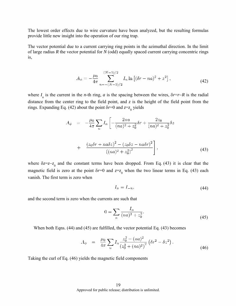
19 Approved for public release; distribution is unlimited.
The lowest order effects due to wire curvature have been analyzed, but the resulting formulas provide little new insight into the operation of our ring trap. The vector potential due to a current carrying ring points in the azimuthal direction. In the limit of large radius R the vector potential for N (odd) equally spaced current carrying concentric rings is,
(42)
where I
n is the current in the n-th ring, a is the spacing between the wires, r=rR is the radial
distance from the center ring to the field point, and z is the height of the field point from the rings. Expanding Eq. (42) about the point r=0 and z=z0 yields
(43)
where z=zz0 and the constant terms have been dropped. From Eq. (43) it is clear that the magnetic field is zero at the point r=0 and z=z0 when the two linear terms in Eq. (43) each vanish. The first term is zero when (44) and the second term is zero when the currents are such that
(45)
When both Eqns. (44) and (45) are fulfilled, the vector potential Eq. (43) becomes
(46) Taking the curl of Eq. (46) yields the magnetic field components
20 Approved for public release; distribution is unlimited.
(47)
Equations (47) show that the magnetic field near the minima is of the same form as a simple single wire wave guide [40, 44], with field gradient given by
(48) Note that the sum still runs from (N1)/2 to (N1)/2. We will now limit our discussion to the case of seven concentric rings, with seven independent currents. Equation (44) eliminates three of the currents, leaving us with four currents independent currents I0, I1, I2 and I3 (As shown in Fig. 6). Initially, the atoms are loaded into a ring trap, i.e. located at 0 rad below the center wire in Fig. 6. To avoid the leads the currents in the wires of the 4-wire trap at this location must be zero, I1=I3=0. To satisfy Eq. (45), the relation between the remaining to currents must be
(49) and the magnetic field gradient is
(50)
When the atomic clouds have propagated half way around the ring trap, they are near the rad in Fig. 6. To avoid the perturbations due to the leads of the 3-wire trap the currents at that position must vanish, I0=I2=0. At this point the trap is formed only by the currents in the wires with current I1 and I3. To satisfy Eq. (45), the relation between the nonzero currents must be
(51)
and the magnetic field gradient is
(52)
21 Approved for public release; distribution is unlimited.
When the atoms are in the region near /2 rad as shown in Fig. 6, there are no input leads and all seven wires can have nonzero current. In this situation Eq. (45) has many solutions, but the simplest solution is to assume that both Eq. (49) and (51) are fulfilled. There are now two free parameters to specify the magnetic field and the field gradient and can be expressed as
(53)
To avoid heating of the atomic gas as it moves around the ring, the magnetic field gradient B' should be held constant. At time t=0, I1=0, and I0=I0(0). To hold the gradient constant, the time dependence of the current I1 should be
(54)
2.4 Switching Between the 3-Wire and 4-Wire Ring Trap
To demonstrate the uniformity of the trapping potential while transferring from the 3-wire guide to the 4-wire guide, plots are given in Figs. 7 and 8 of the magnitude of magnetic field strength in steps of t. In Figs. 7 and 8 , a=50 m, z0=100 m, and the current I
ref=0.5 A was chosen to
give a gradient B'=1000 Gcm. Time dependent currents are given as follows:
(55)
(56)
where t
max=1.0 and t was chosen to allow each waveguide to have values of I
ref between 0 and 1.
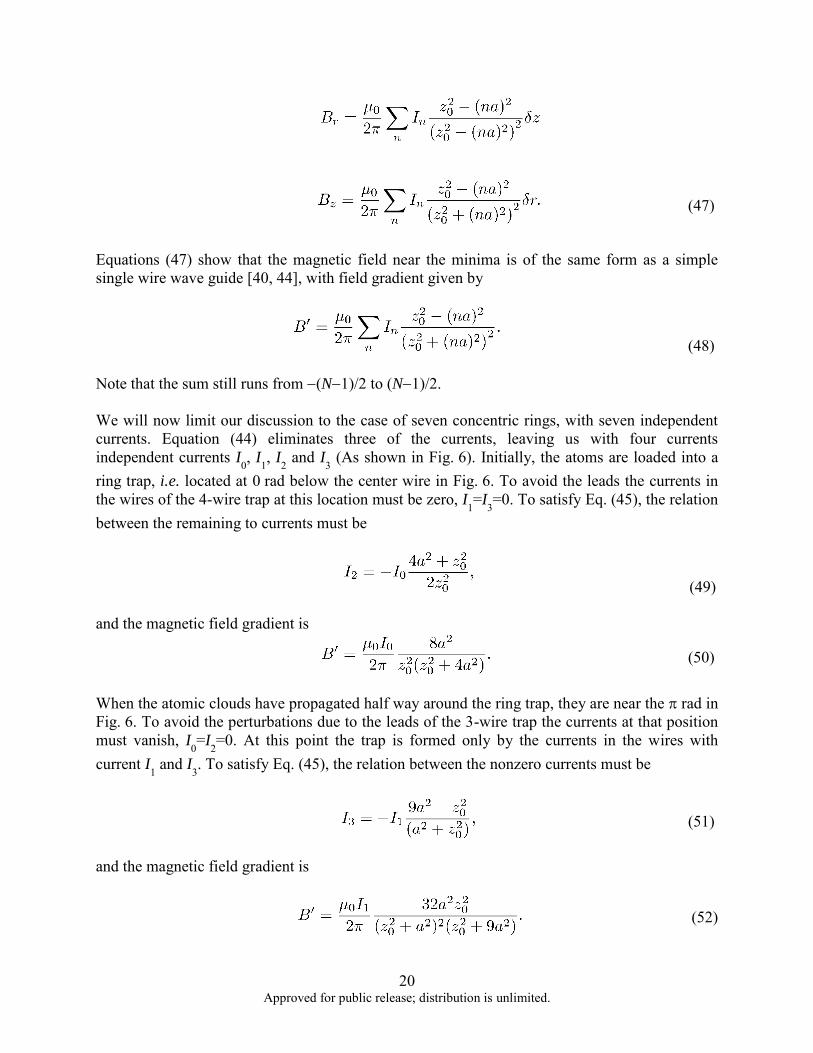
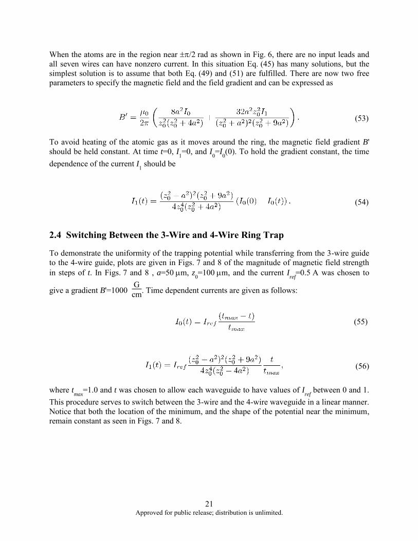
This procedure serves to switch between the 3-wire and the 4-wire waveguide in a linear manner. Notice that both the location of the minimum, and the shape of the potential near the minimum, remain constant as seen in Figs. 7 and 8.
22 Approved for public release; distribution is unlimited.
Figure 7. Trapping Potential in Gauss Along r-Axis for t=01 in Equal Steps
Figure 8. Trapping Potential Below the Wires is Given in Gauss Along z-Axis for t=01 in
Equal Steps
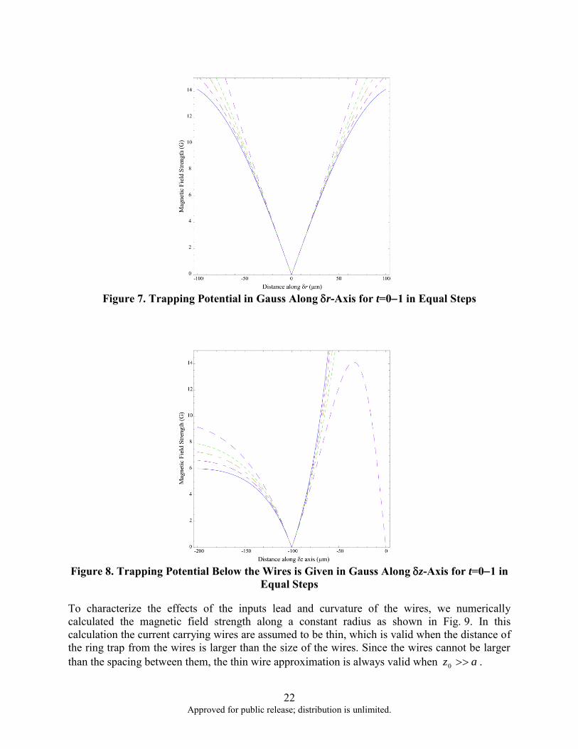
To characterize the effects of the inputs lead and curvature of the wires, we numerically calculated the magnetic field strength along a constant radius as shown in Fig. 9. In this calculation the current carrying wires are assumed to be thin, which is valid when the distance of the ring trap from the wires is larger than the size of the wires. Since the wires cannot be larger than the spacing between them, the thin wire approximation is always valid when az 0 .
23 Approved for public release; distribution is unlimited.
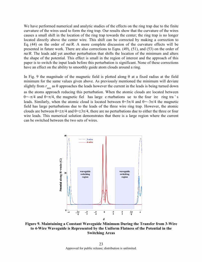
We have performed numerical and analytic studies of the effects on the ring trap due to the finite curvature of the wires used to form the ring trap. Our results show that the curvature of the wires causes a small shift in the location of the ring trap towards the center; the ring trap is no longer located directly above the center wire. This shift can be corrected by making a correction to Eq. (44) on the order of na/R. A more complete discussion of the curvature effects will be presented in future work. There are also corrections to Eqns. (49), (51), and (53) on the order of na/R. The leads add yet another perturbation that shifts the location of the minimum and alters the shape of the potential. This effect is small in the region of interest and the approach of this paper is to switch the input leads before this perturbation is significant. None of these corrections have an effect on the ability to smoothly guide atom clouds around a ring. In Fig. 9 the magnitude of the magnetic field is plotted along at a fixed radius at the field minimum for the same values given above. As previously mentioned the minimum will deviate slightly from r
min as approaches the leads however the current in the leads is being turned down
as the atoms approach reducing this perturbation. When the atomic clouds are located between =/4 and =/4, the magnetic fiel has large e rturbations ue to the four ire ring tra ’ s leads. Similarly, when the atomic cloud is located between =3/4 and =3/4 the magnetic field has large perturbations due to the leads of the three wire ring trap. However, the atomic clouds are between =/4 and =3/4, there are no perturbations due to either the three or four wire leads. This numerical solution demonstrates that there is a large region where the current can be switched between the two sets of wires.
Figure 9. Maintaining a Constant Waveguide Minimum During the Transfer from 3-Wire
to 4-Wire Waveguide is Represented by the Uniform Flatness of the Potential in the Switching Areas
24 Approved for public release; distribution is unlimited.
2.5 Conclusions
We have designed and developed a 7-wire ring trap with adjustable height that encloses area and avoids perturbation from input leads. We have introduced a 1-D theoretical model demonstrating it is possible to fabricate a chip where the currents can be switched between the three and four wire ring trap while holding the minimums location and gradient constant. We have numerically analyzed the effects of the input leads and shown that there is a large switching region where the perturbations due to the input leads of both the three and four wire rings can be avoided. Finally, we have briefly discussed our preliminary results of the effects of the curvature of the wires on the ring trap. The choice of atomic cloud temperature plays a pivotal role in the ring trap operation. Bose Einstein Condensates in microchip waveguides can suffer from fragmentation and de-phasing which are undesirable in atom interferometers. Recently, Bouchoule et. al., [45, 46] has demonstrated a possible solution to the fragmentation issue and it is possible to operate the 7-wire ring trap in a manner that makes use of this technique. A BEC can also have reduced coherence times resulting from potential noise and mean field interactions. The short coherence times resulting from mean field interactions are density dependent [30, 32]; therefore a tightly confined BEC would have additional dispersion and dephasing. The 7-wire ring trap design has the additional feature of an adjustable gradient and by adjusting the gradient and utilizing dilute samples the 7-wire ring trap would be able to reduce the atom-atom interactions. Furthermore a weaker transverse confinement allows for more transverse oscillation which can be used for dispersion management [47]. The ability to adjust the gradient thus affords more experimental flexibility. It is experimentally useful to adjust the ring trap radius, i.e for a choice of interferometer interrogation time. De-coupling of temporal and spatial sources of error is useful for systematically identifying and eliminating sources of noise and atom loss. Also, the possibility of adjusting the radius of the waveguide dynamically allows for the study of the coupling of longitudinal and transverse modes that could be used to damp out transverse oscillations if desired and help overlap the clouds at the recombination point [34, 47]. This concept can be extended to an N-wire ring trap where the radial location of the minimum can be adjusted. Finally it should be remarked that care must be taken during loading of the ring trap. Small shot-to-shot uncertainty in the initial momentum of the atom cloud, resulting from poor loading or coupling is sufficient to mask the small phase shifts resulting from rotation1. The 7-wire ring trap and ring traps in general may require additional loading wires that allow the atom cloud to come to equilibrium before optical splitting.
1 Private communication with Cass Sacket in 2009.
25 Approved for public release; distribution is unlimited.
3 ATOM CHIPS ON DIRECT BONDED COPPER SUBSTRATES
3.1 Introduction
Atom chips have been used in many cold atomic physics experiments including magneto-optical traps [48], magnetic traps [48, 49], waveguides [50, 51], transports [52, 53], Bose-Einstein condensates [54], coherent and incoherent beam splitters [55, 56, 57], and have been integrated with optical elements [29, 58, 59]. Using atom chips for cold neutral atom physics has two main advantages. First, by manipulating atoms 1500 m from the chip wires, high magnetic field gradients can be generated at low power dissipation (<10 W). Second, by using well established lithographic fabrication techniques atom chip wires can be precisely placed to generate well defined magnetic fields. For many applications, e.g. atom interferometry using light pulses, working distances of several hundred microns are common. As shown in the Appendix, power dissipation of a magnetic trap is minimized when the working distance from the top surface of a rectangular wire is z0=0.7h and when the aspect ratio is h/w==0.8, where h is the thickness and w is the width of the wire. Realization of thick h≳100m high quality metalizations with standard lithographic techniques has proven to be technologically challenging, time consuming, and very expensive. For atom chip based magnetic traps that require working distances z0≳100 m, we present the use of direct bonded copper (DBC) substrates for atom chip fabrication. Direct bonded copper is the direct joining of a thin sheet of pure copper to a ceramic substrate [60] and is commonly used in power electronics due to its high current handling and heat dissipation properties. Using DBC for atom chips addresses several atom chip fabrication requirements including power dissipation, ease of fabrication, thick metalizations, and excellent wire adhesion. The power dissipation of DBC atom chips is reduced for two reasons. First, thick, pure copper layers are readily available for DBC substrates with a resistivity equal to bulk copper. Second, the ability to easily produce thick atom chip wires that have a reduced net resistance. Another benefit of using DBC for atom chips is the potential for rapid in-house fabrication with minimal equipment. We have produced moderate quality atom chips in less than eight hours, and high quality wires in approximately one week with most of the time being taken by mask design and printing. By using DBC it is straightforward to fabricate various rectangular wire cross sections or aspect ratios because of the availability of a thick copper layer. Wires with aspect ratio ≳2 can be fabricated by wet etching, and it may be possible to realize high aspect ratio wires 20 using ablative laser micro-machining [61]. To date, most atom chips have been fabricated using a Damscene process, where the wire height and aspect ratio are determined by the photoresist thickness and the metal deposition (electroplating or evaporation) with typical wire heights on the order of 10 m [62, 63, 64, 65, 66, 67, 68]. Thick lithographic wires have been fabricated using thick photoresists [50] or by depositing metal in channels formed in the substrate (e.g. deep reactive ion etching in silicon) but the difficulty of fabrication has made thick wires less common. The thickness of a DBC layer is variable but is commonly as thick as 200 m for high current applications.
26 Approved for public release; distribution is unlimited.
Wire substrate adhesion is another key consideration when fabricating atom chips and this is especially true for thick wires because residual stress from metalization increases the probability of delamination. This problem is most often manifest after the atom chip has been fabricated and is being prepared for use. While this is a technological problem with a known solution (i.e. careful surface preparation) it is a frequent issue that is solved by using DBC. In our experience, it takes considerable effort to remove the copper from the substrate which has made it possible to perform significant post processing of the atom chip. For example, we have mechanically removed selected areas of the ceramic substrate after the copper has been etched so that the chip can be fol e to yiel a t hree im ensional “origami chi ”. In this paper we will discuss basic fabrication methods, the resulting wire quality, and power dissipation. We will show DBC atom chips that are post-processed to make three dimensional chip structures that simplify electrical connections to the atom chip.
3.2 Fabrication of Atom Chips Using Direct Bonded Copper
To make DCB substrates, a copper sheet and a ceramic are bonded using the oxygen-copper eutectic ( 1.5% oxygen at 1065 C ) that is just below the melting point of pure copper (1085C). During bonding, a thin melt layer occurs at the oxide-copper interface that wets the ceramic surface and fills surface irregularities. The resulting bond is very strong because of the surface wetting between the copper and the oxide, and has excellent thermal conductivity because the intermediate liquid stage fills voids between the copper and the substrate. During bonding, the melt layer solidifies as diffusion of copper and oxygen at the interface moves the stoichiometric composition of the melt away from the eutectic transition. To provide enough oxygen for the eutectic transition, a thin ceramic oxide layer on the surface of the copper and ceramic is required. The substrate can be an oxide (e.g. aluminum oxide (Al2O3) or Beryllium oxide (BeO)) or the surface can be oxidized prior to bonding (e.g. Al2O3 formation on aluminum nitride (AlN) or copper oxide on copper), however, the surface oxidation step can reduce the bulk thermal conductivity due to the diffusion of oxygen along grain boundaries [69]. While any oxide can be used for DBC, most applications use electrically insulating substrates that are thermally conductive. Beryllium oxide has the highest thermal conductivity (260 W/mC) of the ceramics, but is not commonly used because of beryllium toxicity. Most DBC substrates are Al2O3 or AlN. Aluminum oxide is commonly used despite a moderate thermal conductivity
(25 W/mC) because of its low cost, high substrate quality, and high bond strength. Aluminum nitride is also used because of its high thermal conductivity (170 W/mC) and a coefficient of thermal expansion (4.7 m/mC) that is closely matched to silicon. Aluminum nitride has previously been used for atom chips with electroplated wires [48] where the wires are in direct and conformal contact with the substrate, however, electroplated metals typically have higher resistivities than the bulk metal and, as a result, the maximum current density is reduced [70]. Additionally, electroplated metals have a grained structure that results in variations of the magnetic field close to the wire [65]. In DBC, the bonded copper maintains the electrical properties of the original copper sheet (i.e. high purity, high density, and low resistivity) for all thicknesses of DBC. The high purity of the DBC permits high total currents
27 Approved for public release; distribution is unlimited.
relative to electroplated wires of the same thickness [69], or for the same current reduced power dissipation. Pure and high density atom chip wires have been deposited via evaporation with bulk resistivity and smooth wire edges [66]. The evaporation process is suitable for thin films (<5 m) but is complicated (e.g. refilling the evaporation source) and inefficient because only a small fraction of the evaporated metal is deposited on the substrate while the remainder sticks to the walls of the vacuum system. Excellent wire to substrate adhesion is a significant practical benefit of DBC atom chips. Atom chips that use electroplated or evaporated wires need an adhesion layer (e.g. Ti, TiW, Cr) to avoid delamination of the atom chip wires. The quality of the adhesion can vary significantly and depends on substrate cleanliness, deposition parameters, and substrate compatibility. Wire adhesion is especially important for thicker wires that may have residual stress from the growth process. The adhesion of DBC is excellent; it takes significant force to remove bulk copper or thin wires from the substrate. Because of the excellent adhesion, atom chips can be modified after patterning (see Sec. 3.3) while maintaining the integrity of the rest of the atom chip. High current hermetic vias is another option made possible by DBC and is a standard option for DBC substrates [71] and have been used as a part of a neutral atom trap [72]. Commercially available vias are incorporated into the substrate during the bonding process and require a custom manufacturing run. It may also be possible to form vias by drilling through the substrate and soldering or electroplating in the hole to form a via. Although there are many potential methods for building a DBC atom chip, the chips in this paper are fabricated by applying a mask to the surface of the DBC and then etching the copper away from the exposed areas leaving wire traces on the AlN substrate. For rapid prototyping (several hours), laser printer toner is used for the mask and the copper is etched with hydrochloric acid plus dilute hydrogen peroxide. For 125 m thick copper this method can reproducibly produce 175 m wide wires with 500 m center to center spacing. The minimum feature size is determined by the resolution of the laser printer and the thickness of the copper. The second fabrication method uses photoresist and a commercially printed mask with sub-micron resolution. After the pattern transfer, using standard lithographic procedures, the wires are etched using either hydrochloric/peroxide or reverse electroplating [73]. For 125 m thick copper this method can reproducibly produce wires widths of 100 m with 250 m spacing. With care wire widths of 50 m with 200 m spacing can be fabricated. Specific processing details of each method follow below. To promote mask adhesion, the DBC surface is first cleaned by scrubbing the surface with steel wool and then rinsing with acetone and methanol. For rapid mask production, laser printer toner provides a chemically resistant thermo-plastic that adheres to a surface when it is melted. The toner may be remelted for multiple transfers between different substrates. A 600 dpi laser printer is used to print the chip design onto a commercially available PCB transfer film 2. The transfer film will release the backing at the areas where the toner sticks to the DBC making it possible to
2An HP LaserJet printer was used for printing the mask. Press-n-Peel and Pulsar toner transfer papers have been used with similar success. Specific vendors are provided for information only. This does not constitute endorsement.
28 Approved for public release; distribution is unlimited.
remo e the original r inting me ia . The toner transfer r oce ur e follo s the manufacturer’s instructions with special care given to the temperature cycling because overheating will result in a distorted toner mask. After etching, the mask is removed with acetone. The advantage of the toner transfer mask is rapid mask production with minimal equipment. The feature size using toner transfer is limited by the printer resolution, the spreading of the toner during transfer, and the DBC thickness. Improved mask quality and smaller wires are achieved using photolithography. First, a silicon nitride layer is applied to the DBC to improve photoresist adhesion. A 20 m photoresist layer (AZ4620 or SU8) is spin coated and then lithographically patterned. Compared to the toner transfer method, the photolithographically defined atom chip wires are significantly straighter and the achievable wire width is significantly narrower (50 m). The sidewall definition and minimum line size is a strong function of the total copper thickness. For the 125 m thick DBC used in this paper, the narrowest line feature that could be reproducibly etched was (50 m). Compared to a toner transfer produced atom chip a lithographically produced atom chip requires more time (multiple days versus hours) and additional equipment, but is able to produce finer features, more consistent lines, and accurate wire placement not possible using a toner mask. Several test chips were etched using solutions of 37% hydrochloric acid (HCl), hydrogen peroxide, and water in a mixture of approximately 5:1:10 by volume. The wire quality depended on the peroxide concentration, etching time, and solution agitation. The hydrogen peroxide concentration was varied from 2 to 0.2 by volume, with lower concentrations yielding longer etching times (1-2 hrs) and the best wires. Solution agitation reduces the etch times by removing bubbles from the surface and provides fresh chemicals to the etching areas. At the end of the etching procedure a pipette was used to provide local agitation to reduce wire footing and assure electrical isolation of the atom chip wires. For low concentrations of hydrogen peroxide (0.4 by volume) no agitation is necessary because of reduced surface bubbles. The acid/hydrogen peroxide etching method is isotropic and causes undercutting of the mask, resulting in a trapezoidal wire shape and a wire width that is smaller than the original mask.
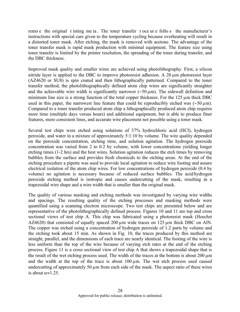
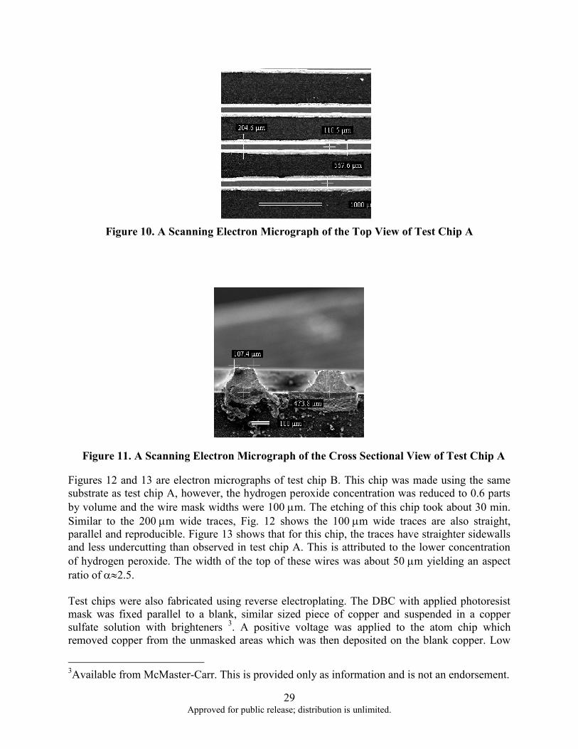
The quality of various masking and etching methods was investigated by varying wire widths and spacings. The resulting quality of the etching processes and masking methods were quantified using a scanning electron microscope. Two test chips are presented below and are representative of the photolithographically defined process. Figures 10 and 11 are top and cross sectional views of test chip A. This chip was fabricated using a photoresist mask (Hoechst AZ4620) that consisted of equally spaced 200 m wide traces on 125 m thick DBC on AlN. The copper was etched using a concentration of hydrogen peroxide of 1.2 parts by volume and the etching took about 15 min. As shown in Fig. 10, the traces produced by this method are straight, parallel, and the dimensions of each trace are nearly identical. The footing of the wire is less uniform than the top of the wire because of varying etch rates at the end of the etching process. Figure 11 is a cross sectional view of test chip A that shows a trapezoidal shape that is the result of the wet etching process used. The width of the traces at the bottom is about 200 m and the width at the top of the trace is about 100 m. The wet etch process used caused undercutting of approximately 50 m from each side of the mask. The aspect ratio of these wires is about 1.25.
29 Approved for public release; distribution is unlimited.
Figure 10. A Scanning Electron Micrograph of the Top View of Test Chip A
Figure 11. A Scanning Electron Micrograph of the Cross Sectional View of Test Chip A
Figures 12 and 13 are electron micrographs of test chip B. This chip was made using the same substrate as test chip A, however, the hydrogen peroxide concentration was reduced to 0.6 parts by volume and the wire mask widths were 100 m. The etching of this chip took about 30 min. Similar to the 200 m wide traces, Fig. 12 shows the 100 m wide traces are also straight, parallel and reproducible. Figure 13 shows that for this chip, the traces have straighter sidewalls and less undercutting than observed in test chip A. This is attributed to the lower concentration of hydrogen peroxide. The width of the top of these wires was about 50 m yielding an aspect ratio of 2.5. Test chips were also fabricated using reverse electroplating. The DBC with applied photoresist mask was fixed parallel to a blank, similar sized piece of copper and suspended in a copper sulfate solution with brighteners 3. A positive voltage was applied to the atom chip which removed copper from the unmasked areas which was then deposited on the blank copper. Low
3Available from McMaster-Carr. This is provided only as information and is not an endorsement.

30 Approved for public release; distribution is unlimited.
current densities (0.5 A/m2) produced the best results, but resulted in increased etching times. A magnetic stirrer was used to provide fresh solution to the surface of the DBC, however, for long etching times the photoresist mask debonded because of the constant agitation of the
Figure 12. A Scanning Electron Micrograph of the Top View of Test Chip B
Figure 13. A Scanning Electron Micrograph of the Cross Sectional View of Test Chip B
electroplating solution. Toward the end of the reverse electroplating, small (10 m diameter) copper islands remain because they were no longer electrically connected. The copper islands were removed by a rapid (<5 min) acid etch. While reverse electroplating has the potential to provide higher aspect ratio wires and close wire placement, the limits of the process are not determined at this time because of the mask integrity. The maximum current handling and the thermal impedance of DBC atom chips was tested by fabricating a test chip with three 1 cm long wires with different widths: 170 m, 230 m, and 340 m. To approximate the reduced thermal dissipation in vacuum, the chip was tested in air without a heat sink. Only the results of the thinnest wire are reported because the heating effects were found to be negligible for the wider wires. The heating (measured using a thermocouple on the substrate 5 mm from the wire) and the voltage drop across the wire, were measured for currents of 10-100 A (0.45109 A/m2). A 2 s current pulse of 100 A (110 W average power) resulted in a 2.7 times increase in the wire resistance and <15 temperature rise. For short times
31 Approved for public release; distribution is unlimited.
(<10 ms) the thermal conductance of the wire/substrate junction was measured to be 112106
W/K-m2, which is approximately 1.5-2 times the wire/substrate junction thermal conductance of silicon with a 20 nm oxide layer [66]. With a suitable heat sink the DBC atom chips should have equal or better performance in vacuum.
3.3 Assembly
We are currently developing a trapped atom interferometer gyroscope [33] that uses a cigar shaped harmonic trap. Our plan is to realize this trap using a two layer DBC atom chip. The chips were fabricated using a toner transfer mask and a HCl/peroxide etch. The chip closest to the atoms (front chip) has four parallel wires that are 200 m wide and spaced 500 m center to center. Figure 14a shows the mask and Fig. 14b is a photograph of the final front chip. The chip farthest from the atoms (back chip) has four parallel wires that are 400 m wide and are separated by 1500 m. The mask and chip for are shown in Figs. 14 c and d. Areas of the chip that would otherwise be open are filled to reduce the amount of etchant used and to maintain a level top surface. The chip wire leads are 2.5 mm wide to reduce power dissipation and provide strength when the substrate is removed in later processing.
a.) b.)
c.) d.) Figure 14. Toner Masks for Etching and Photographs of the Etched Chips
After the atom chips were etched the substrates were modified for making electrical connections by drilling holes 4 at the end of the chip. To improve optical access and to accommodate the space requirements, the edges of the chip were folded back so the electrical connections could be made behind the mounting structure. To avoid stressing and breaking the copper at the bend areas, the AlN substrate was removed with a diamond grinding bit that is 2-3 times wider than the substrate thickness. This is a straight forward and reliable process because the diamond bit removes hard material significantly faster than soft materials (i.e. the AlN can be removed without damaging the copper). The copper traces were deformed by the slight pressure of the diamond grinding bit but have no noticeable degradation in performance. This processing was made possible due to the excellent adhesion of the copper to the substrate and the copper thickness that is readily available using DBC. This can also be accomplished by bonding multiple substrates with appropriate gaps, however this requires minimum lot runs and is not practical for one-off atom chip designs. Perha s the main a a ntage of fol a ble atom chi s ( ubb e “origami chi s”) is that they ermit potentially bulky electrical connections to be made away from the surface of the atom chip. This allows direct connections to be made to the chip while maintaining optical access over the full
4We ha e use iamon r ill bits from Da ’ s Rock Sho a n iamon late g rin in g bits from McMaster-Carr. This is not an endorsement and is for information only.

32 Approved for public release; distribution is unlimited.
range of the chip. High power electrical connections are available to the chip without bond wires, soldering, or vias. The effect of the leads can be easily taken into account because the wires have a well-defined path away from the chip.
Figure 15 is a photograph of a DBC atom chip assembly constructed using two atom chips, shown in Fig. 14, that were processed, folded, stacked, and epoxied to a copper heat sink (using Epotek 353 ND). Four of the wires were connected using vacuum compatible screws. The assembly was placed in an UHV chamber and baked at 130 for approximately one week. After bakeout, the UHV chamber was isolated from the turbo pump and was pumped solely by a 40 l/s ion pump to a final pressure of <21010 torr. A 87Rb MOT was loaded directly below the DBC atom chip assembly and was then compressed and cooled in a compressed MOT. The atoms were magnetically trapped and transported to the DBC atom chip where they were transferred to a chip quadrupole magnetic trap made by running current in the front chip wire plus an appropriate bias field. The ability to quantify the quality of the first chip was limited by the optical quality of the glass vacuum chamber. A new vacuum chamber has been constructed to address the optical quality issues.
Figure 15. Photograph of DBC Atom Chip Assembly on Copper Mounting Post
3.4 Conclusion
Direct bonded copper substrates are an excellent candidate for atom chip fabrication because of thick high purity copper that is intimately bonded to a high thermal conductivity substrate. Direct bonded copper atom chips can support very high currents (at minimum 100 A) for several seconds for high magnetic field gradient traps or for reduced power dissipation at lower currents. Wires with the appropriate cross section will further optimize the magnetic field gradient for a given power dissipation. The fabrication of DBC atom chips is straight forward and requires very little equipment. Direct bonded copper atom chips are very robust and can be bent to form 3D atom chip structures that simplify the electrical connections away from the chips or for precision wire placement in multiple dimensions. While this paper demonstrates the initial design and use of DBC for atom chips, there are multiple avenues for future improvements, such as, other copper patterning techniques (laser etching or dry etching [74]) which could produce higher density and/or higher aspect ratio wires.

33 Approved for public release; distribution is unlimited.
Additionally, high precision and high current coils can be made for precise generation of centimeter size magnetic fields. The DBC can also be patterned as a thermally conductive carrier for atom chips with finely patterned lithographic wires [53]. The ability to form vias in the DBC also allows for greater flexibility in chip designs and for the potential to make high power hermetic feedthroughs.

34 Approved for public release; distribution is unlimited.
REFERENCES
[1] Durfee, D. S., Shaham, Y. K., and Kasevich, M. A., “Long-Term Stability of an Area-
Reversible Atom-Interferometer Sagnac Gyrosco e ,” Physical Review Letters, 97, Dec 2006, pp. 240801(1)-240801(R).
[2] Hogan, J. M., Johnson, D. M. S., and Kasevich, M. A., “Light-Pulse Atom Interferometry,”
arXiv:0806.3261v1, Jun 2008, pp.1-38. [3] Peters, A., Chung, K. Y., and Chu, S., “Measurement of Gravitational Acceleration by
Dro ing Atoms,” Nature, 400, 1999, pp. 849-852. [4] Schumm, T., Hofferberth, S., Andersson, L. M., Wildermuth, S., Groth, S., Bar-Joseph,
I., Schmiedmayer, J., and Kruger, P., “Matter-wave Interferometry in a Double Well on an Atom Chi ,” Nature Physics, 1, 2005, pp. 57-62.
[5] Wang, Y.-J., Anderson, D. Z., Bright, V. M., Cornell, E. A., Diot, Q., Kishimoto, T.,
Prentiss, M., Saravanan, R. A., Segal, S. R., and Wu, S., “An Atom Michelson Interferometer on a Chip Using a Bose-Einstein Con e nsate,” Physical Review Letters, 94, 2005, pp. 090405(1)-090405(4).
[6] Garcia, O., Deissler, B., Hughes, K. J., Reeves, J. M., and Sackett, C. A., “Bose-Einstein
Con e nsate Interferometer ith Macrosco ic Arm Se a ration,” Physical Review A, 74, 2006, pp. 031601(1)-031601(4).
[7] Horikoshi, M., and Nakagawa, K., “De h asing Due to an Atom-Atom Interaction in a
Waveguide Interferometer Using a Bose-Einstein Con e nsate,” Physical Review A, 74, 2006, pp. 031602(1)-031602(R).
[8] Jo, G.-B., Shin, Y., Will, S., Pasquini, T. A., Saba, M., Ketterle, W., Pritchard, D. E.,
Vengalattore, M., and Prentiss, M., “Long Phase Coherence Time an Number Squeezing of Two Bose-Einstein Con ensates on an Atom Chi ,” Physical Review Letters, 98, 2007, pp. 030407(1)-030407(4).
[9] Wu, S., Su, E., and Prentiss, M. “Demonstration of an Area-Enclosing Guided-Atom
Interferometer for Rotation Sensing,” Physical Review Letters, 99, 2007, pp. 173201. [10] Deissler, B., Hughes, K. J., Burke, J. H. T., and Sackett, C. A., “Measurement of the AC
Stark Shift with a Guided Matter- a e Interferometer,” Physical Review A, 77, 2008, pp. 031604(1)- 031604(8).
[11] Javanainen, J., and Wilkens, M., “Phase an Phase Diffusion in a S li t Bose-Einstein
Con e nsate,” Physical Review Letters, 78, 1997, pp. 4675-4678.
35 Approved for public release; distribution is unlimited.
[12] Leggett, A. J., and Sols, F., “Comment on ‘Phase an Phase Diffusion of a S li t Bose-Einstein Condensate’,” Physical Review Letters, 81, 1998, pp. 1344.
[13] Javanainen, J., and Wilkens, M., “Ja a nainen an Wilkens Re l y:,” Physical Review
Letters, 81, 1998, pp. 1345. [14] Cronin, A. D., Schmiedmayer, J., and Pritchard, D. E., “Atom Interferometers,”
arXiv:0712.3703v1 Dec 2007, pp. 1-82. [15] Cahn, S. B., Kumarakrishnan, A., Shim, U., Sleator, T., Berman, P. R., and Dubetsky, B.,
“Time-Domain De Broglie Wa e Interferometery,” Physical Review Letters, 79, 1997, pp. 784-787.
[16] Horikoshi, M., and Nakagawa, K., “Su re ssion of De h asing Due to a Tra ing Potential
and Atom-Atom Interactions in a Trapped-Condensate Interferometer,” Physical Review
Letters, 99, 2007, pp. 180401. [17] Wu, S., Striehl, P. S., and Prentiss, M. G., “A Weyl Function A r oach to Matter-wave
Coherence and Talbot-Lau Effects,” arXiv:0710.5479v2, 2007, pp. 1-38. [18] Burke, J. H. T., Deissler, B., Hughes, K. J., and Sackett, C. A., “Confinement Effects in a
Guided-Wave Atom Interferometer with Millimeter-Scale Arm Se a ration,” Physical
Review A, 78, 2008, pp. 023619(1)- 023619(9). [19] Stickney, J. A., Kafle, R. P., Anderson, D. Z., and Zozulya, A. A., “Theoretical Analysis of
a Single and Double Reflection Atom Interferometer in a Weakly Confining Magnetic Tra ,” Physical Review A, 77, 2008, pp. 043604(1)- 043604(9).
[20] Su, E. J., Wu, S., and Prentiss, M. G., “Atom Interferometry Using Wavepackets with
Constant S a tial Dis lacements,” arXiv:physics/0701018v2, 2008, pp. 1-13. [21] Stickney, J. A., Anderson, D. Z., and Zozulya, A. A., “Increasing the Coherence Time of
Bose-Einstein Condensate Interferometers with Optical Control of Dynamics,” Physical
Review A, 75, 2007, pp. 063603(1)- 063603(12). [22] A. Akhiezer and S. Peletminskii, Methods of Statistical Physics, Pergamon Press, Oxford,
1981. [23] S. Chapman and T. Cowling, The Mathematical Theory of Non-Uniform Gases 3rd ed.,
Cambridge at the University Press, Cambridge, 1970. [24] A. L. Garcia, Numerical Methods for Physicists 2nd ed., Prentice Hall, New Jersey, 2000. [25] Gustavson, T. L., Bouyer, P., and Kasevich, M. A., “Precision Rotation Measurements it h
an Atom Interferometer Gyrosco e,” Physical Review Letters, 78, 1997, pp. 2046-2049.

36 Approved for public release; distribution is unlimited.
[26] Lenef, A., Hammond, T. D., Smith, E. T., Chapman, M. S., Rubenstein, R. A., and Pritchard, D. E., “Rotation Sensing ith an Atom Interferometer,” Physical Review Letters, 78, 1997, pp. 760-763.
[27] Wu, S., Su, E., and Prentiss, M., “Demonstration of an Area-Enclosing Guided-Atom
Interferometer for Rotation Sensing,” Physical Review Letters, 99, 2007, pp. 173201(1)- 173201(4).
[28] Shin, Y., Pasquini, T. A., Pritchard, D. E., and Leanhardt, A. E., “Atom Interferometry ith
Bose-Einstein Condensates in a Double-Well Potential,” Physical Review Letters, 92, 2004, pp. 050405(1)- 050405(4).
[29] Wang, Y., Anderson, D., Bright, V. M., Cornell, E. A., Diot, Q., Kishimoto, T., Prentiss, M.,
Saravanan, R. A., Segal, S. R., and Wu, S., “Atom Michelson Interferometer on a Chi Using a Bose-Einstein Con e nsate,” Physical Review Letters, 94, 2005, pp. 090405(1)- 090405(4).
[30] Garcia, O., Deissler, B., Hughes, K. J., Reeves, J. M., and Sackett, C. A., “Bose-Einstein
Con e nsate Interferometer ith Macrosco ic Arm Se a ration,” Physical Review A, 74, 2006, pp. 031601(1)- 031601(4).
[31] Gustavson, T. L., Landragin, A., and Kasevich, M. A., “Rotation Sensing ith a Dual
Atom-Interferometer Sagnac Gyrosco e,” Classical Quantum Gravity, 17, 2000, pp. 2385-2398.
[32] Horikoshi, M., and Nakagawa, K., “De ha sing Due to Atom-Atom Interaction in a
Waveguide Interferometer Using a Bose-Einstein Con e nsate,” Physical Review A, 74, 2006, pp. 031602(1)- 031602(4).
[33] Stickney, J. A., Squires, M. B., Scoville, J., Baker, P., and Miller, S., “Collisional
Decoherence in Trapped-Atom Interferometers That Use Non e generate Sources,” Physical
Review A, 79, 2009, pp. 013618(1)- 013618(8). [34] Gupta, S., Murch, K. W., Moore, K. L., Purdy, T. P., and Stamper-Kurn, D. M., “Bose-
Einstein Con e nsation in a Circular Wa e gui e ,” Physical Review Letters, 95, 2005, pp. 143201(1)- 143201(4).
[35] Griffin, P. F., Riis, E., and Arnold, A. S., “Smooth In uc ti e ly Cou le Ring Trap for
Atoms,” Physical Review A, 77, 2008, pp. 051402(1)- 051402(4). [36] Crookston, M. B., Baker, P. M., and Robinson, M. P., “A Microchi Ring Tra for Col
Atoms,” Journal of Physics B, 38, 2005, pp. 3289-3298. [37] Arnold, A. S., Garvie, C. S., and Riis, E., “Large Magnetic Storage Ring for Bose-Einstein
Con e nsates,” Physical Review A, 73, 2006, pp. 041606(1)- 041606(4).

37 Approved for public release; distribution is unlimited.
[38] Lin, Y., Teper, I., Chin, C., and Vuletić, V., “Im a ct of the Casimir-Polder Potential and Johnson Noise on Bose-Einstein Con e nsate Stability Near Surfaces,” Physical Review
Letters, 92, 2004, pp. 050404(1)- 050404(4). [39] Cassettari, D., Hessmo, B., Folman, R., Maier, T., and Schmiedmayer, J., “Beam S li tter for
Gui e Atoms ,” Physical Review Letters, 85, 2000, pp. 5483-5487. [40] Thywissen, J. H., Olshanii, M., Drn ić, M., Westervelt, R. M., and Prentiss, M.,
“Microfabricate Magnetic Wa e gui es for Nuetral Atoms,” European Physics D, 7, 1999, pp. 361-367.
[41] Sagnac, G., “L'èther Lumineux Dèmontrè Par L'effet Du Vent Relatif D'èther Dans Un
Interfèromètre En Rotation Uniforme,” C. R. Acadamie Scientifique. 95, 1913, pp. 708-710. [42] Post, E. J., “Sagnac Effect,” Review of Modern Physics, 39, 1967, pp. 475-493. [43] Petrich, W., Anderson, M. H., Ensher, J. R., and Cornell, E. A., “Stable, Tightly Confining
Magnetic Tra for E a orati e Cooling of Neutral Atoms,” Physical Review Letters, 74, 1995, pp. 3352-3355.
[44] Fortagh, J., and Zimmermann, C., “Magnetic Microtra s for Ultracol Atoms,” Review of
Modern Physics, 79, 2007, pp. 235-289. [45] Trebbia, J., Garrido Alzar, C. L., Cornelussen, R., Westbrook, C. I., and Bouchoule, I.,
“Roughness Su re ssion Via Ra i Current Mo ul ation on an Atom Chi ,” Physical
Review Letters, 98, 2007, pp. 263201(1)- 263201(4). [46] Bouchoule, I., Trebbia, J. B., and Garrido Alzar, C. L., “Limitations of the Mo ul ations
Method to Smooth Wire-Gui e Roughness,” Physical Review A, 77, 2008, pp. 023624(1)- 023624(11).
[47] Murch, K. W., Moore, K. L., Gupta, S., and Stamper-Kurn, D. M., “Dis e rsion Management
Using Betatron Resonances in an Ultracold-Atom Storage Ring,” Physical Review Letters, 96, 2006, pp. 013202(1)- 013202(4).
[48] Reichel, J., Hänsel, W., and Hänsch, T. W., “Atomic Micromani ul ation ith Magnetic
Surface Tra s,” Physical Review Letters, 83, 1999, pp. 3398-3401. [49] Weinstein, J. D., and Libbrecht, K. G., “Microsco ic Magnetic Tra s for Neutral Atoms,”
Physical Review A, 52, 1995, pp. 4004-4009. [50] Müller, D., Anderson, D. Z., Grow, R. J., Schwindt, P. D. D., and Cornell, E. A., “Gui ing
Neutral Atoms Around Curves with Lithographically Patterned Current-Carrying Wires,” Physical Review Letters, 83, 1999, pp. 5194-5197.

38 Approved for public release; distribution is unlimited.
[51] Luo, X., Kr¨uger, P., Brugger, K., Wildermuth, S., Gimpel, H., Klein, M. W., Groth, S., Folman, R., Bar-Jose h , I., an Schmie ma yer, J., “Atom Fiber for Omnidirectional Gui ing of Col Ne utral Atoms,” Optics Letters, 29, Sep 2004, pp. 2145-2147.
[52] Hänsel, W., Reichel, J., Hommelhoff, P., and Hänsch, T. W., “Magnetic Con e yor Belt for
Trans ortin g an Merging Tra e Atom Clou s ,” Physical Review Letters, 86, 2001, pp. 608-611.
[53] Günther, A., Kemmler, M., Kraft, S., Vale, C. J., Zimmermann, C., and Fortágh, J.,
“Combine Chi s for Atom O tics,” Physical Review A, 71, 2005, pp. 063619(1)- 063619(8).
[54] Hänsel, W., Hommelhoff, P., Reichel, J., and Hänsch, T. W., “Bose-Einstein Condensation
on a Microelectronic Chi ,” Nature, 413, 2001, pp. 498-501. [55] Cassettari, D., Hessmo, B., Folman, R., Maier, T., and Schmiedmayer, J., “Beam S litter for
Gui e Atoms ,” Physical Review Letters, 85, 2000, pp. 5483-5487. [56] Schumm, T., Hofferberth, S., Andersson, L. M., Wildermuth, S., Groth, S., Bar-Joseph,
I., Schmiedmayer, J., and Kruger, P., “Matter-Wave Interferometry in a Double Well on an Atom Chi ,” Nature Physics, 1, 2005, pp. 57-62.
[57] Shin, Y., Sanner, C., Jo, G. B., Pasquini, T. A., Saba, M., Ketterle, W., Pritchard,
D. E., Vengalattore, M., and Prentiss, M., “Interference of Bose-Einstein Condensates Split ith an A tom Chi ,” Physical Review A, 72, 2005, pp. 021604(1)- 021604(4).
[58] Teper, I., Lin, Y. J., and Vuletić, V., “AMANDA Obser a tions Contrain the Ultrahigh
Energy Neutrino Flux,” Physical Review Letters, 97, 2006, pp. 023002(1)- 023002(4). [59] Purdy, T., and Stamper-Kurn, D., “Integrating Cavity Quantum Electrodynamics and
Ultracold-Atom Chips with on-Chip Dielectric Mirrors and Temperature Stabilization,” Applied Physics B, 90, 2008, pp. 401-405.
[60] J. F. Burgess and C. A. Neugebauer, US Patent #3911553 (1975). [61] Karnakis, D., Rutterford, G., and Knowles, M. R. H., “High Po e r DPSS Laser
Micromachining of Silicon an Stainless Steel,” Third International WLT-Conference on
Lasers in Manufacturing, Munich, Germany, Jun 2005. [62] Fortagh, J., Grossmann, A., Zimmermann, C., and Hänsch, T. W., “Miniaturize Wire Tra
for Neutral Atoms,” Physical Review Letters, 81, 1998, pp. 5310-5313. [63] Reichel, J., Hänsel, W., Hommelhoff, P., and Hänsch, T. W., “A lic ations of Integrate
Magnetic Microtra s,” Applied Physics B: Lasers and Optics, 72, 2001, pp. 81-89.

39 Approved for public release; distribution is unlimited.
[64] Drn ić, M., Johnson, K. S., Thywissen, J. H., Prentiss, M., and Westervelt, R. M., “Micro-Electromagnets for Atom Mani ul ation,” Applied Physics Letters 72, 1998, pp. 2906-2909.
[65] Estève, J., Aussibal, C., Schumm, T., Figl, C., Mailly, D., Bouchoule, I., Westbrook, C. I.,
and Aspect, A., “Role of Wire Im er fections in Micromagnetic Tra s for Atoms,” Physical
Review A, 70, 2004, pp. 043629(1)- 043629(4). [66] Groth, S., Krüger, P., Wildermuth, S., Folman, R., Fernholz, T., Schmiedmayer, J., Mahalu,
D., and Bar-Joseph, I., “Atom Chi s: Fabrication an Thermal Pro e rties,” Applied Physics
Letters, 85, 2004, pp. 2980-2983. [67] Ju Lin, Y., Teper, I., Chin, C., and Vuletićć, V., “Im a ct of the Casimir-Polder Potential and
Johnson Noise on Bose-Einstein Con e nsates Stability Near Surfaces,” Physical Review
Letters, 92, 2004, pp. 050404(1)- 050404(4). [68] Horikoshi, M., and Nakagawa, K., “Atom Chi Base Fast Pro uc tion of Bose-Einstein
Con e nsate,” Applied Physics B: Lasers and Optics, 82, 2006, pp. 363-366. [69] W. W. Sheng and R. P. Colino, Power Electronic Modules: Design and Manufacture,
CRC Press, 2004. [70] Teh, W. H., Koh, L. T., Chen, S. M., Xie, J., Li, C. Y., and Foo, P. D., “Stu y of
Microstructure and Resistivity Evolution for Electroplated Copper Films at Near-Room Tem er ature,” Microelectronics Journal, 32, 2001, pp. 579-585.
[71] Schulz-Harder, J., and Exel, K., “Recent developments of direct bonded copper (DBC)
substrates for power modules,” Fifth International Conference on Electronic Packaging
Technology, Shanghai, China, 2003. [72] Wang, R., Liu, M., Minardi, F., and Kasevich, M., “Reaching Li7 Quantum Degeneracy
With a Minitra ,” Physical Review A, 75, 2007, pp. 013610(1)- 013610(7). [73] X. Liu, Ph.D. thesis, “Processing an Reliability Assessment of Sol er Joint Interconnection
for Po e r Chi s ,” Virginia Polytechnic Institute and State University (2001). [74] Lee, J. W., Park, Y. D., Childress, J. R., Pearton, S. J., Sharifi, F., and Ren, F., “Co e r Dry
Etching with Cl2/Ar Plasma Chemistry,” Journal of The Electrochemical Society, 145, 1998, pp. 2585-2589.
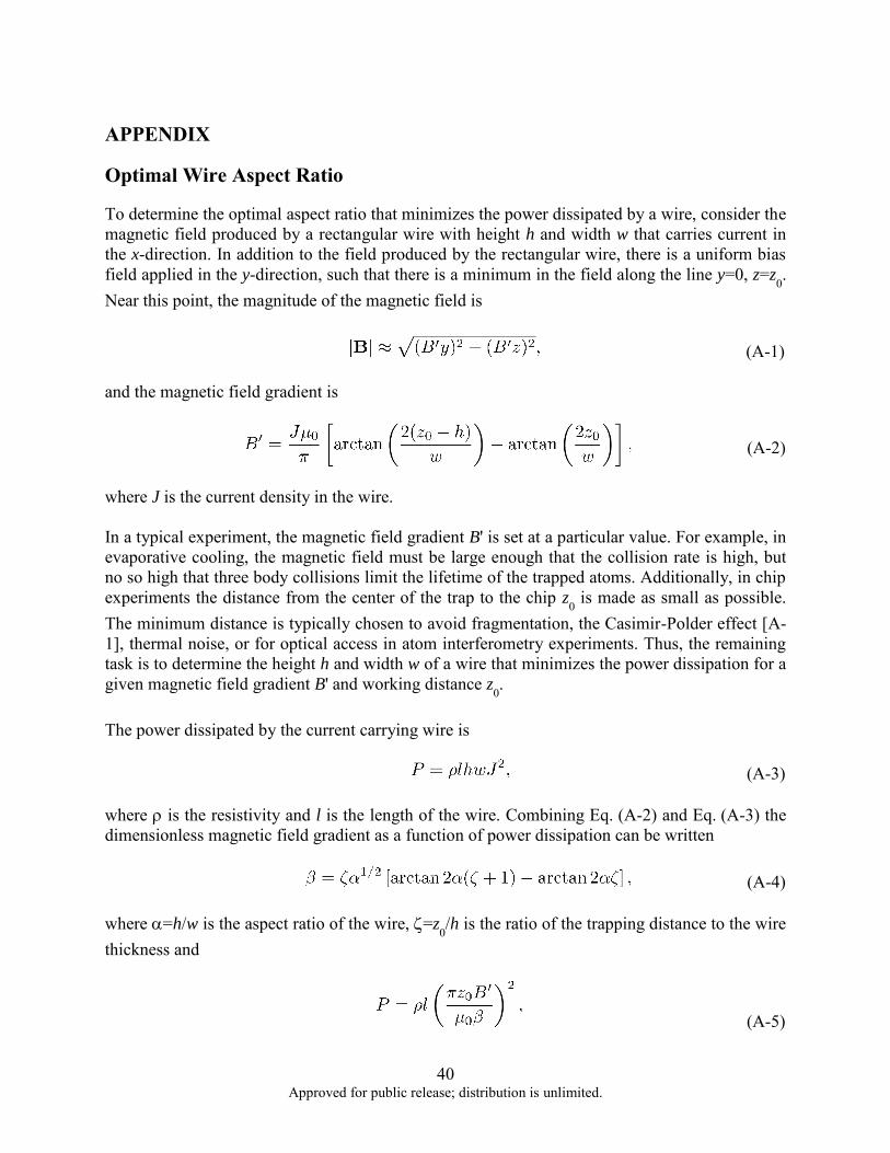
40 Approved for public release; distribution is unlimited.
APPENDIX
Optimal Wire Aspect Ratio
To determine the optimal aspect ratio that minimizes the power dissipated by a wire, consider the magnetic field produced by a rectangular wire with height h and width w that carries current in the x-direction. In addition to the field produced by the rectangular wire, there is a uniform bias field applied in the y-direction, such that there is a minimum in the field along the line y=0, z=z0. Near this point, the magnitude of the magnetic field is (A-1) and the magnetic field gradient is
(A-2)
where J is the current density in the wire. In a typical experiment, the magnetic field gradient B' is set at a particular value. For example, in evaporative cooling, the magnetic field must be large enough that the collision rate is high, but no so high that three body collisions limit the lifetime of the trapped atoms. Additionally, in chip experiments the distance from the center of the trap to the chip z0 is made as small as possible. The minimum distance is typically chosen to avoid fragmentation, the Casimir-Polder effect [A-1], thermal noise, or for optical access in atom interferometry experiments. Thus, the remaining task is to determine the height h and width w of a wire that minimizes the power dissipation for a given magnetic field gradient B' and working distance z0. The power dissipated by the current carrying wire is
(A-3) where is the resistivity and l is the length of the wire. Combining Eq. (A-2) and Eq. (A-3) the dimensionless magnetic field gradient as a function of power dissipation can be written (A-4) where =h/w is the aspect ratio of the wire, =z0/h is the ratio of the trapping distance to the wire thickness and
(A-5)
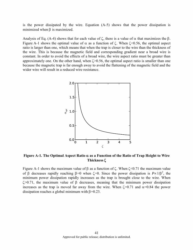
41 Approved for public release; distribution is unlimited.
is the power dissipated by the wire. Equation (A-5) shows that the power dissipation is minimized when is maximized. Analysis of Eq. (A-4) shows that for each value of , there is a value of that maximizes the . Figure A-1 shows the optimal value of as a function of . When <0.56, the optimal aspect ratio is larger than one, which means that when the trap is closer to the wire than the thickness of the wire. This is because the magnetic field and corresponding gradient near a broad wire is constant. In order to avoid the effects of a broad wire, the wire aspect ratio must be greater than approximately one. On the other hand, when >0.56, the optimal aspect ratio is smaller than one because the magnetic trap is far enough away to avoid the flattening of the magnetic field and the wider wire will result in a reduced wire resistance.
Figure A-1. The Optimal Aspect Ratio as a Function of the Ratio of Trap Height to Wire
Thickness
Figure A-1 shows the maximum value of as a function of . When <0.71 the maximum value of decreases rapidly reaching =0 when =0. Since the power dissipation is P1/2, the minimum power dissipation rapidly increases as the trap is brought close to the wire. When >0.71, the maximum value of decreases, meaning that the minimum power dissipation increases as the trap is moved far away from the wire. When =0.71 and =0.84 the power dissipation reaches a global minimum with =0.23.
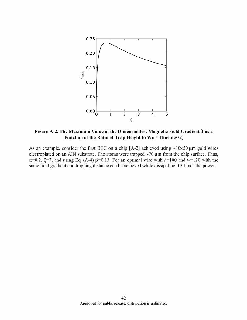
42 Approved for public release; distribution is unlimited.
Figure A-2. The Maximum Value of the Dimensionless Magnetic Field Gradient as a
Function of the Ratio of Trap Height to Wire Thickness
As an example, consider the first BEC on a chip [A-2] achieved using 1050 m gold wires electroplated on an AlN substrate. The atoms were trapped 70 m from the chip surface. Thus, =0.2, =7, and using Eq. (A-4) =0.13. For an optimal wire with h=100 and w=120 with the same field gradient and trapping distance can be achieved while dissipating 0.3 times the power.
43 Approved for public release; distribution is unlimited.
APPENDIX REFERENCES [A-1] Ju Lin, Y., Teper, I., Chin, C., and Vuletićć, V., “Im a ct of the Casimir-Polder Potential
and Johnson Noise on Bose-Einstein Con e nsates Stability Near Surfaces,” Physical Review
Letters, 92, 2004, pp. 050404(1)- 050404(4). [A-2] Hänsel, W., Hommelhoff, P., Reichel, J., and Hänsch, T. W., “Bose-Einstein
Condensation on a Microelectronic Chi ,” Nature, 413, 2001, pp. 498-501.

44 Approved for public release; distribution is unlimited.
List of Acronyms
BEC Bose-Einstein Condensate
BeO Beryllium Oxide
DBC Direct Bonded Copper
DPI Dots Per Inch
DSMC Direct Simulation Monte-Carlo
MOT Magneto-Optical Trap
PCB Printed Circuit Board
TOP Time-Orbiting Potential
UHV Ultra High Vacuum

45 Approved for public release; distribution is unlimited.
DDIISSTTRRIIBBUUTTIIOONN LLIISSTT
DDTTIICC//OOCCPP 88772255 JJoohhnn JJ.. KKiinnggmmaann RRdd,, SSuuiittee 00994444 FFtt BBeellvvooiirr,, VVAA 2222006600--66221188 11 ccyy AAFFRRLL//RRVVIILL KKiirrttllaanndd AAFFBB,, NNMM 8877111177--55777766 22 ccyyss OOffffiicciiaall RReeccoorrdd CCooppyy AAFFRRLL//RRVVBBYYEE//SStteevveenn MMiilllleerr 11 ccyy

46 Approved for public release; distribution is unlimited.
This page is intentionally left blank.