atmel at42qt1110-mz...
TRANSCRIPT
Atmel AT42QT1110-MZAT42QT1110-AZ
11-key QTouch® Touch Sensor IC
DATASHEET
Features
Sensor Keys: Up to 11 QTouch® channels
Data Acquisition: Measurement of keys triggered either by a signal applied to the SYNC pin or
at regular intervals timed by the AT42QT1110 internal clock Keys measured sequentially for better performance, or in parallel groups for
faster operation Raw data for key touches can be read as a report over the SPI interface
Discrete Outputs: Configurable “Detect” outputs indicating individual key touch (7-key mode)
Device Setup: Device configuration can be stored in EEPROM
Technology: Patented spread-spectrum charge-transfer (direct mode)
Key Outline Sizes: 6 mm × 6 mm or larger (panel thickness dependent); widely different sizes and
shapes possible, including solid or ring shapes
Key Spacings: 7 mm center-to-center or more (panel thickness dependent)
Layers Required: One
Electrode Materials: Etched copper, silver, carbon, Indium Tin Oxide (ITO)
Electrode Substrates: PCB, FPCB, plastic films, glass
Panel Materials: Plastic, glass, composites, painted surfaces (low particle density metallic
paints possible)
Panel Thickness: Up to 10 mm glass, 5 mm plastic (electrode size dependent)
Key Sensitivity: Individually settable via simple commands over serial interface
Adjacent Key Suppression® (AKS®) Patented AKS technology to enable accurate key detection
Interface: Full-duplex SPI slave mode (1.5 MHz), CHANGE pin, discrete detection
outputs
9570J–AT42–05/2013

Moisture Tolerance Increased moisture tolerance based on hardware design and firmware tuning
Power: 3 V – 5.5 V
Package: 32-pin 5 × 5 mm MLF RoHS compliant 32-pin 7 × 7 mm TQFP RoHS compliant
Signal Processing: Self-calibration, auto drift compensation, noise filtering, AKS technology
Applications: Specific package qualified for automotive applications, such as radio, keyless entry, electric windows and satellite
navigation
2AT42QT1110-MZ / AT42QT1110-AZ [DATASHEET]9570J–AT42–05/2013

1. Pinout and Schematic
1.1 Pinout Configuration
1.2 Pin Descriptions
SN
S0
SN
S10
K/S
YN
C
SN
S10
/DE
TE
CT
6
RE
SE
T
CH
AN
GE
SN
S9/
DE
TE
CT
4
SN
S8K
/DE
TE
CT
3
SN
S3K
SN
S4
SN
S4K
SN
S5K SS
MO
SI
MIS
O
SNS0K
SNS1
SNS1K
VDD
VSS
SNS2K
SNS3 SCK
VDD
SNS6K
SNS6
VSS
SNS7K/DETECT0
SNS7/DETECT1
SNS8/DETECT21
2
3
4
5
6
7
8 17
18
19
20
21
22
23
2432 31 30 29 28 27 26 25
9 10 11 1615141312
SN
S5
SNS2S
NS
9K/D
ET
EC
T5
QT1110QT1110
Table 1-1. Pin Listing
Pin Name Type Comments If Unused, Connect To...
1 SNS0K I/O Sense Pin Leave open
2 SNS1 I/O Sense Pin Leave open
3 SNS1K I/O Sense Pin Leave open
4 Vdd P Power –
5 Vss P Supply Ground –
6 SNS2K I/O Sense Pin Leave open
7 SNS2 I/O Sense Pin Leave open
8 SNS3 I/O Sense Pin Leave open
9 SNS3K I/O Sense Pin Leave open
10 SNS4 I/O Sense Pin Leave open
11 SNS4K I/O Sense Pin Leave open
3AT42QT1110-MZ / AT42QT1110-AZ [DATASHEET]9570J–AT42–05/2013

I Input only I/O Input and outputO Output only, push-pull OD Open drain output P Ground or power
12 SNS5 I/O Sense Pin Leave open
13 SNS5K I/O Sense Pin Leave open
14 SS I Enable SPIVss via 100 k resistor to enable SPI
Vdd via 100 k resistor to disable SPI
15 MOSI I SPI Data In Leave open
16 MISO O SPI Data Out Leave open
17 SCK I SPI Clock Leave open
18 Vdd P Power –
19 SNS6K I/O Sense Pin Leave open
20 SNS6 I/O Sense Pin Leave open
21 Vss P Supply Ground –
22 SNS7K/DETECT0 I/O Sense Pin/Key Status Indicator Leave open
23 SNS7/DETECT1 I/O Sense Pin/Key Status Indicator Leave open
24 SNS8/DETECT2 I/O Sense Pin / Key Status Indicator Leave open
25 SNS8K/DETECT3 I/O Sense Pin / Key Status Indicator Leave open
26 SNS9/DETECT4 I/O Sense Pin / Key Status Indicator Leave open
27 SNS9K/DETECT5 I/O Sense Pin / Key Status Indicator Leave open
28 CHANGE OD Touch Event Indicator Leave open
29 RESET I Reset Vdd
30 SNS10/DETECT6 I/O Sense Pin / Key Status Indicator Leave open
31 SNS10K/SYNC I/O Sense Pin / Synchronization Input Vdd or Vss via 100 k resistor
32 SNS0 I/O Sense Pin Leave open
Table 1-1. Pin Listing (Continued)
Pin Name Type Comments If Unused, Connect To...
4AT42QT1110-MZ / AT42QT1110-AZ [DATASHEET]9570J–AT42–05/2013

1.3 Schematics
Figure 1-1. Typical Circuit: 7 keys With Detect Outputs and No External Trigger
VREG
Vunreg
QT
111
0
5AT42QT1110-MZ / AT42QT1110-AZ [DATASHEET]9570J–AT42–05/2013

Figure 1-2. Typical Circuit: 11 Keys With No External Trigger
Vunreg VREG
QT1110
6AT42QT1110-MZ / AT42QT1110-AZ [DATASHEET]9570J–AT42–05/2013

Figure 1-3. Typical Circuit: 10 Keys With External Trigger (SYNC Mode)
For component values in Figure 1-1, Figure 1-2 and Figure 1-3, check the following sections:
Section 3.1 on page 9: Cs capacitors (Cs0 – Cs10)
Section 3.2 on page 9: Sample resistors (Rs0 – Rs10)
Section 3.5 on page 10: Voltage levels
Section 3.3 on page 9: LED traces
VREGVunreg
QT1110
7AT42QT1110-MZ / AT42QT1110-AZ [DATASHEET]9570J–AT42–05/2013

2. Overview of the AT42QT1110
2.1 Introduction
The AT42QT1110 (QT1110) is a digital burst mode charge-transfer (QT™) capacitive sensor driver designed for anytouch-key applications.
The keys can be constructed in different shapes and sizes. Refer to the Touch Sensors Design Guide andApplication Note QTAN0002, Secrets of a Successful QTouch Design, for more information on construction anddesign methods (both downloadable from the Atmel website).
The device includes all signal processing functions necessary to provide stable sensing under a wide variety ofchanging conditions, and the outputs are fully debounced. Only a few external parts are required for operation.
The QT1110 modulates its bursts in a spread-spectrum fashion in order to suppress heavily the effects of externalnoise, and to suppress RF emissions.
2.2 Configurations
The QT1110 is designed as a versatile device, capable of various configurations. There are two basic configurationsfor the QT1110:
11-key QTouch. The device can sense up to 11 keys.
7-key QTouch with individual outputs for each key. The device can sense up to 7 keys and drive the matching Detect outputs to a user-configurable PWM.
Both configurations allow for a choice of acquisition modes, thus providing a variety of possibilities that will satisfymost applications (see the following sections for more information).
Additionally, the SYNC line can be used as an external trigger input. Note that in 11-key mode the SYNC linereplaces one key, thus allowing only 10 keys.
See Section 4.7 on page 18 for more information.
2.3 Guard Channel
The device has a guard channel option (available in all key modes), which allows one key to be configured as aguard channel to help prevent false detection. See Section 4.9 on page 20 for more information.
2.4 Self-test Functions
The QT1110 has two types of self-test functions:
Internal Hardware tests – check for hardware failures in the device internal memory.
Functional checks – confirm that the device is operating within expected parameters.
See Section 4.10 on page 20 for more information.
2.5 Moisture Tolerance
The presence of water (condensation, sweat, spilt water, and so on) on a sensor can alter the signal valuesmeasured and thereby affect the performance of any capacitive device. The moisture tolerance of QTouch devicescan be improved by designing the hardware and fine-tuning the firmware following the recommendations in theapplication note Atmel AVR3002: Moisture Tolerant QTouch Design (www.atmel.com/Images/doc42017.pdf).
8AT42QT1110-MZ / AT42QT1110-AZ [DATASHEET]9570J–AT42–05/2013

3. Wiring and Parts
3.1 Cs Sample Capacitors
Cs0 – Cs10 are the charge sensing sample capacitors. Normally they are identical in nominal value. The optimal Csvalues depend on the thickness of the panel and its dielectric constant. Thicker panels require larger values of Cs.Values can be in the range 2.2 nF (for faster operation) to 33 nF (for best sensitivity); typical values are 4.7 nF to10 nF.
The value of Cs should be chosen so that a light touch on a key produces a reduction of ~20 to 30 in the key signalvalue (see Section 6.8 on page 27). The chosen Cs value should never be so large that the key signals exceed~1000, as reported by the chip in the debug data.
The Cs capacitors must be X7R or PPS film type, for stability. For consistent sensitivity, they should have a 10percent tolerance. Twenty percent tolerance may cause small differences in sensitivity from key to key and unit tounit. If a key is not used, the Cs capacitor may be omitted.
3.2 Rs Resistors
The series resistors Rs0 – Rs10 are inline with the electrode connections and should be used to limit electrostaticdischarge (ESD) currents and to suppress radio frequency (RF) interference. Values should be approximately 2 kto 20 k each; a typical value is 4.7 k.
Although these resistors may be omitted, the device may become susceptible to external noise or radio frequencyinterference (RFI). For details of how to select these resistors see the Application Note QTAN0002, Secrets of aSuccessful QTouch Design, downloadable from the Touch Technology area of the Atmel website, www.atmel.com.
3.3 LED Traces and Other Switching Signals
Digital switching signals near the sense lines can induce transients into the acquired signals, deteriorating the SNRperformance of the device. Such signals should be routed away from the sensing traces and electrodes, or thedesign should be such that these lines are not switched during the course of signal acquisition (bursts).
LED terminals which are multiplexed or switched into a floating state, and which are within, or physically very near, akey (even if on another nearby PCB) should be bypassed to either Vss or Vdd with at least a 1 nF capacitor. This isto suppress capacitive coupling effects which can induce false signal shifts. The bypass capacitor does not need tobe next to the LED, in fact it can be quite distant. The bypass capacitor is noncritical and can be of any type.
LED terminals which are constantly connected to Vss or Vdd do not need further bypassing.
3.4 PCB Cleanliness
Modern no-clean flux is generally compatible with capacitive sensing circuits.
CAUTION: If a PCB is reworked to correct soldering faults relating to the QT1110, or to any associated traces or components, be sure that you fully understand the nature of the flux used during the rework process. Leakage currents from hygroscopic ionic residues can stop capacitive sensors from functioning. If you have any doubts, a thorough cleaning after rework may be the only safe option.
9AT42QT1110-MZ / AT42QT1110-AZ [DATASHEET]9570J–AT42–05/2013

3.5 Power Supply
3.5.1 General Considerations
See Section 8.2 on page 39 for the power supply range. If the power supply fluctuates slowly with temperature, thedevice tracks and compensates for these changes automatically with only minor changes in sensitivity. If the supplyvoltage drifts or shifts quickly, the drift compensation mechanism is not able to keep up, causing sensitivityanomalies or false detections.
The usual power supply considerations with QT parts apply to the device. The power should be clean and come froma separate regulator if possible. However, this device is designed to minimize the effects of unstable power, and,except in extreme conditions, should not require a separate Low Dropout (LDO) regulator.
See underneath Figure 1.3 on page 5 for suggested regulator manufacturers.
It is assumed that a larger bypass capacitor (like1 µF) is somewhere else in the power circuit; for example, near theregulator.
3.5.2 Brownout Detection
The QT1110 includes a power supply monitoring circuit that detects if Vdd drops below a safe operating voltage.When this occurs, the device goes into a Reset state, where no acquisition or processing is carried out. The deviceremains in this state until Vdd returns to the specified voltage range.
Once a safe operating voltage is detected, the QT1110 behaves as per normal power-on/reset conditions; that is,any saved settings are restored from EEPROM, the internal self-tests are run and all channels are calibrated.
The Brown-out detector threshold is 2.7 V ±10%.
3.6 MLF Package Restrictions
The central pad on the underside of the MLF chip should be connected to ground. Do not run any tracks underneaththe body of the chip, only ground. Figure 3-1 shows examples of good and bad tracking.
Figure 3-1. Examples of Good and Bad Tracking
Caution: A regulator IC shared with other logic can result in erratic operation and is not advised.
A single ceramic 0.1 µF bypass capacitor, with short traces, should be placed very close to the power pins of the IC. Failure to do so can result in device oscillation, high current consumption, or erratic operation.
Example of GOOD tracking Example of BAD tracking
10AT42QT1110-MZ / AT42QT1110-AZ [DATASHEET]9570J–AT42–05/2013

4. Detailed Operations
4.1 Communications
4.1.1 Introduction
All communication with the device is carried out over the Serial Peripheral Interface (SPI). This is a synchronousserial data link that operates in full-duplex mode. The host communicates with the QT controller over the SPI using amaster-slave relationship, with the QT1110 acting in slave mode.
4.1.2 SPI Operation
The SPI uses four logic signals:
Serial Clock (SCK) – output from the host.
Master Output, Slave Input (MOSI) – output from the host, input to the QT controller. Used by the host to send data to the QT controller.
Master Input, Slave Output (MISO) – input to the host, output from the QT controller. Used by the QT device to send data to the host.
Slave Select (SS) – active low output from the host.
At each byte, the master pulls SS low and generates 8 clock pulses on SCK. With these 8 clock pulses, a byte ofdata is transmitted from the master to the slave over MOSI, most significant bit (msb) first.
Simultaneously a byte of data is transmitted from the slave to the master over MISO, also most significant bit first.
The slave reads the status of MOSI at the leading edge of each clock pulse, and the master reads the slave datafrom MISO at the trailing edge.
The QT1110 requires that the clock idles “high”, meaning that the data on MOSI and MISO pins are set at the fallingedges and sampled at the rising edges.
That is:
Clock polarity CPOL = 1Clock phase CPHA = 1
The QT1110 SPI interface can operate at any SCK frequency up to 1.5 MHz.
In multibyte communications, the master must pause for a minimum delay of 150 µs between the completion of onebyte exchange and the beginning of the next.
Note that the number of bytes to be transmitted depends on the initial command sent by the host. This sets the modeon the QT1110 so that the QT1110 knows how to respond to, or how to interpret, the following bytes. If there is adelay of >100 ms between bytes while the QT1110 is waiting for data, or waiting to send data, then the incompletetransmission is discarded and the device resets its SPI state machine. It will then interpret the next byte it receives asa fresh command.
When the QT1110 SPI interface is receiving a new command, it returns the Idle status code (0x55) on MISO duringthe first byte exchange to indicate to the master that it is in the correct state for receiving instructions.
4.1.3 CRC Bytes
If enabled, a CRC checking procedure is implemented on all communications between the SPI master and theQT1110. In this case, each command or report request sent by the master must have a byte appended containingthe CRC checksum of the data sent. The QT1110 will not respond to commands until the CRC byte has beenreceived and verified.
Sample C code showing the algorithm for calculating the CRC of the data can be found in Appendix A..
11AT42QT1110-MZ / AT42QT1110-AZ [DATASHEET]9570J–AT42–05/2013

When the QT1110 is expecting a CRC byte, it returns (on MISO) the calculated CRC byte which it expects toreceive. This is sent simultaneously with the QT1110 receiving the CRC byte from the master (that is, during thesame byte exchange). This allows both devices to confirm that the data was sent correctly.
All data returned by the QT1110 is also be followed by a CRC byte, allowing the master to confirm the integrity of thedata transmission.
4.1.4 SPI Commands
There are three types of communication between the SPI master and the QT1110:
Control commands (see Section 5. on page 22)
To send control instructions to the QT1110
Report requests (see Section 6. on page 25)
To reading status information from the QT1110
Setup commands (see Section 7. on page 29)
To set configuration options (“Set” instructions)
To read configuration options (“Get” instructions)
Additionally the NULL command (0x00) is transmitted by the host device as it is receiving data from the QT1110.
4.1.4.1 Control Commands
A control command is an instruction sent to the QT1110 that controls operations of the device, and for which noresponse is required. Examples of control commands are: Reset, Calibrate, Send Setups.
With the exception of Send Setups, control commands normally require a single byte exchange, unless CRCchecking is enabled, in which case a second byte must be transmitted by the host with the calculated CRC of thecommand byte.
Figure 4-1. Sleep Command – CRC Disabled
Figure 4-2. Sleep Command – CRC Enabled
Host (Sends on MOSI) Device (Responds on MISO)
SimultaneousTransmission
Command: 0x05
Response: 0x55 ( Idle” Fresh Command)“ –
Host (Sends on MOSI)
Command: 0x05
SimultaneousTransmission
Command CRC: 0x3F
Response: 0x3F (Expected Command CRC)
Response: 0x55 ( Idle” Fresh Command)“ –
Device (Responds on MISO)
12AT42QT1110-MZ / AT42QT1110-AZ [DATASHEET]9570J–AT42–05/2013

When the Send Setups command is received, the QT1110 stops measurement of QTouch sensors and waits for 42bytes of data to be sent. Only when all 42 bytes have been received (and the CRC byte, if CRC is enabled), theQT1110 applies all the settings to RAM and resumes measurement. In this case, if CRC is enabled, the CRC byte iscalculated for all the data sent by the host, including the command byte 0x01.
Control Commands are specified in detail in Section 5. on page 22.
4.1.5 Report Requests
Report Requests are sent by the Host to instruct the QT1110 to return status information. The host sends theappropriate Report Request command, then transmits Null bytes on MOSI while the QT1110 returns the report dataon MISO.
Figure 4-3. All Keys Report – CRC Disabled
For example, Figure 4-3 shows the exchange that takes place to read the 2-byte All Keys report. In this exchange,the host sends:
0xC1 — 0x00 — 0x00
and the QT1110 returns (simultaneously):
0x55 — Report Byte 0 — Report Byte 1
If CRC is enabled, this exchange is extended to 5 bytes, as shown in Figure 4-4 on page 14.
Host (Sends on MOSI)
Command: 0xC1
Device (Responds on MISO)
Null: 0x00
Key Status Report Byte 0
Null: 0x00
Key Status Report Byte 1
SimultaneousTransmissionResponse: 0x55 ( Idle” Fresh Command)“ –
13AT42QT1110-MZ / AT42QT1110-AZ [DATASHEET]9570J–AT42–05/2013
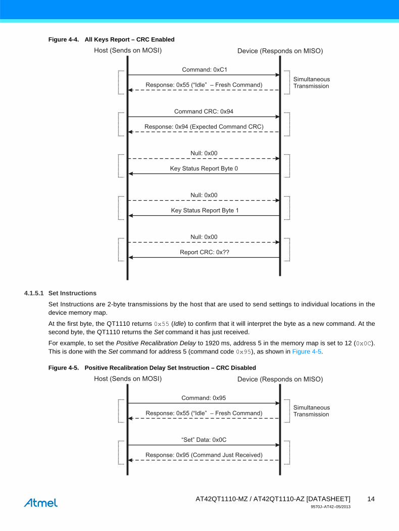
Figure 4-4. All Keys Report – CRC Enabled
4.1.5.1 Set Instructions
Set Instructions are 2-byte transmissions by the host that are used to send settings to individual locations in thedevice memory map.
At the first byte, the QT1110 returns 0x55 (Idle) to confirm that it will interpret the byte as a new command. At thesecond byte, the QT1110 returns the Set command it has just received.
For example, to set the Positive Recalibration Delay to 1920 ms, address 5 in the memory map is set to 12 (0x0C).This is done with the Set command for address 5 (command code 0x95), as shown in Figure 4-5.
Figure 4-5. Positive Recalibration Delay Set Instruction – CRC Disabled
Host (Sends on MOSI)
Command: 0xC1
Null: 0x00
Key Status Report Byte 0
Null: 0x00
Key Status Report Byte 1
Null: 0x00
Report CRC: 0x??
SimultaneousTransmission
Command CRC: 0x94
Response: 0x94 (Expected Command CRC)
Response: 0x55 ( Idle” Fresh Command)“ –
Device (Responds on MISO)
Host (Sends on MOSI)
Command: 0x95
“Set” Data: 0x0C
Response: 0x95 (Command Just Received)
SimultaneousTransmissionResponse: 0x55 ( Idle” Fresh Command)“ –
Device (Responds on MISO)
14AT42QT1110-MZ / AT42QT1110-AZ [DATASHEET]9570J–AT42–05/2013

With CRC Enabled, a CRC byte is also required (Figure 4-6). This is calculated for the two transmitted bytes (that is,the Set command and the data byte).
For example, for the sequence shown in Figure 4-5 (0x95 — 0x0C), the CRC Byte is 0x9F. As is the case with theother command types, when the QT1110 is expecting a CRC byte from the host, it calculates that byte in advanceand returns the expected value to the host in the same transmission as the host sends the CRC byte.
The sent data is not applied to the memory location until the CRC byte has been received and verified.
Figure 4-6. Positive Recalibration Delay Set Instruction – CRC Enabled
4.1.5.2 Get Instructions
Get instructions are instructions that read the data from a location in the QT1110 memory map.
Figure 4-7. Positive Recalibration Delay Get Instruction – CRC Disabled
The host sends the appropriate Get command, followed by a Null byte. The QT1110 returns the contents of theaddressed memory location.
Figure 4-7 shows the exchange for a report on the positive recalibration delay (assuming that the data byte is 0x0C).
With CRC Enabled, this exchange takes 4 bytes, with a command CRC transmitted by the host and a report CRCreturned by the QT1110 (see Figure 4-8 on page 16).
Host (Sends on MOSI)
Command: 0x95
“Set” Data: 0x0C
Response: 0x95 (Command Just Received)
SimultaneousTransmission
Command CRC: 0x9F
Response: 0x9F (Expected CRC)
Response: 0x55 ( Idle” Fresh Command)“ –
Device (Responds on MISO)
Host (Sends on MOSI)
Command: 0xD5
Null: 0x00
“Get” Data: 0x0C (Positive Recalibration Delay)
SimultaneousTransmissionResponse: 0x55 ( Idle” Fresh Command)“ –
Device (Responds on MISO)
15AT42QT1110-MZ / AT42QT1110-AZ [DATASHEET]9570J–AT42–05/2013
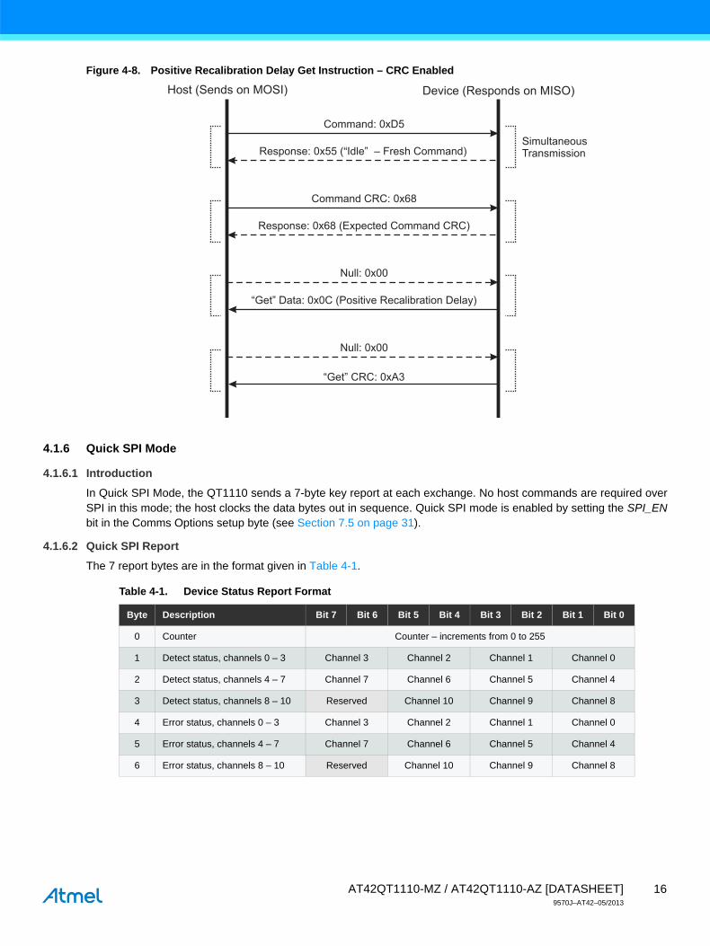
Figure 4-8. Positive Recalibration Delay Get Instruction – CRC Enabled
4.1.6 Quick SPI Mode
4.1.6.1 Introduction
In Quick SPI Mode, the QT1110 sends a 7-byte key report at each exchange. No host commands are required overSPI in this mode; the host clocks the data bytes out in sequence. Quick SPI mode is enabled by setting the SPI_ENbit in the Comms Options setup byte (see Section 7.5 on page 31).
4.1.6.2 Quick SPI Report
The 7 report bytes are in the format given in Table 4-1.
Host (Sends on MOSI)
Command: 0xD5
Null: 0x00
Null: 0x00
“Get” CRC: 0xA3
SimultaneousTransmission
Command CRC: 0x68
Response: 0x68 (Expected Command CRC)
“Get” Data: 0x0C (Positive Recalibration Delay)
Response: 0x55 ( Idle” Fresh Command)“ –
Device (Responds on MISO)
Table 4-1. Device Status Report Format
Byte Description Bit 7 Bit 6 Bit 5 Bit 4 Bit 3 Bit 2 Bit 1 Bit 0
0 Counter Counter – increments from 0 to 255
1 Detect status, channels 0 – 3 Channel 3 Channel 2 Channel 1 Channel 0
2 Detect status, channels 4 – 7 Channel 7 Channel 6 Channel 5 Channel 4
3 Detect status, channels 8 – 10 Reserved Channel 10 Channel 9 Channel 8
4 Error status, channels 0 – 3 Channel 3 Channel 2 Channel 1 Channel 0
5 Error status, channels 4 – 7 Channel 7 Channel 6 Channel 5 Channel 4
6 Error status, channels 8 – 10 Reserved Channel 10 Channel 9 Channel 8
16AT42QT1110-MZ / AT42QT1110-AZ [DATASHEET]9570J–AT42–05/2013

where:
Byte 0 is a counter that increments from 0 to 254 on successive exchanges to confirm that firmware is operating correctly.
Bytes 1 – 3 indicate the detect status of channels 0 – 3, 4 – 7 and 8 – 10 respectively (two bits per channel), as follows:
00 = Channel not in detect
01 = Channel in detect
10 = Not Allowed
11 = Invalid Signal (Channel disabled)
Bytes 4 – 6 indicate the error status of channels 0 – 3, 4 – 7 and 8 – 10 respectively (two bits per channel), as follows:
00 = No error
01 = Not allowed
10 = Error on channel
11 = Invalid signal (channel disabled)
Successive byte exchanges in Quick SPI mode cycle through the 7 bytes of status information. If synchronization islost, the host must either re-synchronize by identifying the incrementing counter byte (byte 0) or pausingcommunications for at least 100 ms so the QT1110 will reset its SPI state.
4.1.6.3 Commands in Quick SPI Mode
Only two host commands are recognized under Quick SPI mode. These are shown in Table 4-2.
CRC checking is not implemented in Quick SPI mode for host commands or return data.
4.1.6.4 Quick SPI Mode timing
In Quick SPI mode, the minimum time between byte exchanges is reduced to 50 µS.
If a pause in communications of 100 ms is detected during reading of the 7-byte report, the QT1110 resets theexchange, and on the next byte read it returns byte 0 of the report.
4.2 Reset
The QT1110 can be reset using one of two methods:
Hardware reset: An external reset logic line can be used if desired, fed into the RESET pin. However, under most conditions it is acceptable to tie RESET to Vdd.
Software reset: A software reset can be forced using the “Reset” control command.
For both methods, the device will follow the same initialization sequence. If there any saved settings in theEEPROM, these are loaded into RAM. Otherwise the default settings are applied.
Note: The SPI interface becomes active after the QT1110 has completed its startup sequence, taking approximately 160 ms after power on/reset.
Table 4-2. Host Commands in Quick SPI Mode
Command Code Purpose
Store to EEPROM 0x0A Allows for “Quick SPI mode” to be stored as the default start-up mode
Enable Full SPI 0x36 Enables full SPI mode
17AT42QT1110-MZ / AT42QT1110-AZ [DATASHEET]9570J–AT42–05/2013
4.3 Sleep Mode
The QT1110 can be put into a very low power sleep mode (typically < 2 µA). During sleep mode, no keys aremeasured and the DETECT outputs are all put into high impedance mode to minimize current consumption. Thedevice remains in sleep mode until a falling edge is detected on either the SS pin or the CHANGE pin. When theQT1110 wakes from sleep mode, it continues to operate as it was before it was put into sleep mode. The QT1110requires approximately 100 µs to wake from sleep mode and will not respond correctly to SPI communications untilthe wake-up procedure is complete. The low level on the SS or CHANGE pin that is used to wake the device must bemaintained for 100 µs to ensure correct operation.
Note: If the device is set to sleep mode for an extended period, the host should initiate a recalibration immediately after waking the QT1110.
4.4 Calibration
The device can be forced to recalibrate the sensor keys at any time. This can be useful where, for example, aportable device is plugged into mains power, or during product development when settings are being tuned.
The QT1110 can also be configured to automatically recalibrate if it remains in detection for too long. This avoidskeys becoming “stuck” after a prolonged period of uninterrupted detection. See Section 7.18 on page 38 for details.
4.5 CHANGE Pin
The CHANGE pin can be configured using the Comms Options setup byte (see Section 7.5 on page 31) to act in oneof two modes:
Data mode
The CHANGE pin is asserted (pulled low) when the detection status of a key changes from that last sent to the host; that is when a key-touch or key-release event occurs.
The CHANGE pin is pulled low when a key status changes and is only released when the “Send All keys” report is requested (0xC1), or the key status information bytes are read in Quick SPI mode (see Section 7.5 on page 31).
Touch mode
The CHANGE pin is pulled low when one or more keys are in detect. The CHANGE pin remains low as long as there is a key in detect, regardless of communications.
The CHANGE pin is released when there are no keys in detect. No host communications are required to release the CHANGE pin.
4.6 Stand-alone Mode
The QT1110 can operate in a stand-alone mode without the use of the SPI interface. The settings are loaded fromEEPROM and the device operates in 7-key mode using the Detect outputs.
4.7 Key Modes
4.7.1 11-key Mode
In 11-key mode, the device can sense up to 11 keys. Alternatively, one key can be replaced by the SYNC line as anexternal trigger input (see Section 4.8.2 on page 19).
11-key mode is configured by setting the MODE bit in the Device Mode setup byte (see Section 7.4 on page 30).
Key acquisition can be triggered in one of two ways: using the internal clock to trigger acquisition either at a fixedrepetition period or in a continuous “free run” mode (see Section 4.8.1), or using the SYNC pin to provide an externaltrigger (see Section 4.8.2 on page 19),
18AT42QT1110-MZ / AT42QT1110-AZ [DATASHEET]9570J–AT42–05/2013

4.7.2 7-key Mode
In 7-key mode, the detect outputs DETECT0 to DETECT6 become active on pins 22 – 27 and 30. These outputsprovide configurable PWM signals that indicate when each of the keys is touched.
7-key mode is configured by clearing the MODE bit in the Device Mode setup byte (see Section 7.4 on page 30).
Each DETECT output can be individually configured to output a PWM signal while the matching key is in detect orout of detect. This signal can be one of nine levels, ranging from low (PWM = 0%) to high (PWM = 100%). Thisallows for the use of an indicating LED. This is achieved by enabling the appropriate bit in the Key to LED setup byte(see Section 7.14 on page 36), and setting the desired outputs levels or PWMs in setup addresses 9 to 15 (seeSection 7.12 on page 34).
4.8 Trigger Modes
4.8.1 Timed Trigger
In 11-key mode, The QT1110 can be configured to use the internal clock as a timed trigger. In this case, the QT1110is configured with a cycle period, such that each acquisition cycle starts a specified length of time after the start ofthe previous cycle. If the cycle period is set to 0, each acquisition cycle starts as soon as the previous one hasfinished, resulting in the acquisition cycles running back-to-back in a “free run” mode.
The use of a timed trigger, and the cycle period to be used, is set in the Device Mode setup byte (see Section 7.4 onpage 30).
4.8.2 Synchronized Trigger
In 11-key mode, if a time trigger is not enabled, the QT1110 operates in “synchronized” mode. In this mode, SNS10Kis used as a SYNC pin to trigger key acquisition, rather than using the device internal clock. In this case themaximum number of keys is reduced to 10.
The SYNC pin can use one of two methods to trigger key measurements, selectable via bit 4 of the Device Modesetup byte (see Section 7.4 on page 30): Low Level and Rising Edge.
With the Low Level method the QT1110 operates in “free run” mode for as long as the SYNC pin is read as a logical0. When the SYNC pin goes high, the current measurement cycle will be finished and no more key measurementswill be taken until the SYNC pin goes low again. The low level trigger should be a minimum of 1 ms so that there issufficient time for the device to detect the low level.
With the Rising Edge method all enabled keys are measured once when a rising edge is detected on the SYNC pin.This allows key measurements to be synchronized to an external event or condition.
For example, the SYNC pin can be used by the host to synchronize several devices to each other. This would ensurethat only one of the devices outputs pulses at any given time and signals from one QT1110 do not interfere with themeasurements from another.
Another use for synchronizing to the rising edge is to steady the signals when the device is running off a mainstransformer with insufficient mains frequency filtering that is causing a 50 Hz or 60 Hz ripple on Vdd. If the mainsvoltage is scaled down with a simple voltage divider and connected to the SYNC pin, then the key measurement canbe triggered by the rising edge detected at a positive going zero-crossing. Note that in this case, each key signal willbe taken at the same point in the cycle, so Vdd will be the same at each measurement for a given key and thesignals will be steadier.
19AT42QT1110-MZ / AT42QT1110-AZ [DATASHEET]9570J–AT42–05/2013

4.9 Guard Channel Option
The device has a guard channel option (available in all key modes), which allows one key to be configured as aguard channel to help prevent false detection (see Figure 4-9 on page 20). Guard channel keys should be moresensitive than the other keys (physically bigger or larger Cs), subject to burst length limitations (see Section 4.11.2on page 21).
With guard channel enabled, the designated key is connected to a sensor pad which detects the presence of touchand overrides any output from the other keys using the chip AKS feature. The guard channel option is enabled by theGuard Key setup byte (see Section 7.5 on page 31).
With the guard channel not enabled, all the keys work normally.
Note: If a key is already “in detect” when the guard channel becomes active, that key will remain in detect and the guard key will not activate until the active key goes out of detect.
Figure 4-9. Guard Channel Example
4.10 Self-test Functions
4.10.1 Internal Hardware Tests
Internal hardware tests check for hardware failure in the device internal memory areas and data paths. Any failuredetected in the function or contents of application ROM, RAM or registers causes the device to reset itself.
The application code is scanned with a CRC check routine to confirm that the application data is all correct.
The RAM and registers are checked periodically (every 10 seconds) for dynamic and static failures.
4.10.2 Functional Checks
Functional checks confirm that the device is operating within expected parameters; any failure detected in thesetests is notified to the system host. The device will continue to operate in the event that such functional failures aredetected.
The functional tests are:
Check that the channel-measurement signals are within the defined range.
Confirm that data stored in the EEPROM is valid.
These tests are carried out as the particular functions are used. For example, the EEPROM is checked when thedevice attempts to load data from EEPROM, and the channel signals are checked when a measurement is carriedout.
Note: If a particular channel is unused, the threshold of that channel should be set to 0 to prevent the incorrect reporting of the unused channel as being in an error state.
Guard ChannelFormed of One Key
Key Pad Formedof Six Keys
20AT42QT1110-MZ / AT42QT1110-AZ [DATASHEET]9570J–AT42–05/2013

4.11 Signal Processing
4.11.1 Detection Integrator
The device features a detection integration mechanism, which acts to confirm a detection in a robust fashion. A per-key counter is incremented each time the key has exceeded its threshold. When this counter reaches a preset limitthe key is finally declared to be touched. For example, if the DI limit is set to 10, then a key signal must fall by morethan the key threshold, and remain below that level for 10 acquisitions, before the key is declared to be touched.
Similarly, the DI is applied to a key that is going out of detect: it must take 10 acquisitions where the signal has notexceeded its detect threshold before it is declared to leave touch.
4.11.2 Burst Length Limitations
The maximum burst length is 2048 pulses. The recommended design is to use a capacitor that gives a signal of<1000 pulses.
The number of pulses in the burst can be obtained by reading the key signal (that is, the number of pulses tocomplete measurement of the key signal) over the SPI interface (see Section 6.8 on page 27). Alternatively, a scopecan be used to measure the entire burst, and then the burst length divided by the time for a single pulse.
Note that the keys are independent of each other. It is therefore possible, for example, to have a signal of 100 on onekey and a signal of 1000 on another.
4.11.3 Adjacent Key Suppression Technology
The device includes the Atmel patented Adjacent Key Suppression (AKS) technology to allow the use of tightlyspaced keys on a keypad with no loss of selectability by the user.
AKS is enabled or disabled for each key individually; only one key out of those enabled for AKS may be reported astouched at any one time. The first key touched dominates and stays in detect until it is released, even if anotherstronger key is reported. Once it is released, the next strongest key is reported. If two keys are simultaneouslydetected, the strongest key is reported, allowing a user to slide a finger across multiple keys with only the dominantkey reporting touch.
Each key can be enabled for AKS processing via the AKS mask (see Section 7.11 on page 34). Keys outside thegroup of enabled keys may be in detect simultaneously.
21AT42QT1110-MZ / AT42QT1110-AZ [DATASHEET]9570J–AT42–05/2013

5. Control Commands
5.1 Introduction
The QT1110 control commands are those commands that affect the device operation.
The control commands are listed in Table 5-1 and are described individually in the following sections.
Note: Commands are implemented immediately upon reception, so a suitable delay is required for the operation to be completed before communications can be re-established.
5.2 Send Setups (0x01)
This command initiates the upload of the full settings table to the QT1110 (see Section 7. on page 29).
When this command is received, the QT1110 stops key measurement and waits until 42 bytes of setup data havebeen received. Key acquisition will restart after all the setup data has been received.
If enabled, a CRC check byte is transmitted (both ways) after the 42 bytes to confirm that they have been receivedcorrectly.
If CRC checking is not enabled, it is recommended that the host request a dump of setup data from the QT1110, andconfirms that the data correctly matches the data sent.
The host must wait for at least 150 µs for the operation to be completed before communications can bere-established.
5.3 Calibrate All (0x03)
This command initiates the recalibration of all sensor keys.
The host must wait for at least 150 µs for the operation to be completed before communications can bere-established.
Table 5-1. Control Commands
Command Code Note
Send Setups 0x01 Configures the device to receive setup data
Calibrate All 0x03 Calibrates all keys
Reset 0x04 Resets the device
Sleep 0x05 Sleep (dead) mode
Store to EEPROM 0x0A Stores RAM setups to EEPROM
Restore from EEPROM 0x0B Copies EEPROM setups to RAM (automatically done at startup)
Erase EEPROM 0x0C Erases EEPROM setups
Recover EEPROM 0x0D Restores last EEPROM settings (after erase)
Calibrate Key k 0x1k Calibrates one key (key k)
22AT42QT1110-MZ / AT42QT1110-AZ [DATASHEET]9570J–AT42–05/2013

5.4 Reset (0x04)
The Reset command forces the QT1110 to reset. If the setups data is present in the EEPROM, the setups areloaded into the device. Otherwise default settings are applied.
The host must wait for at least 160 ms for the operation to be completed before communications can bere-established.
5.5 Sleep (0x05)
The Sleep command puts the device into sleep mode (see Section 4.3 on page 18).
The host must wait for at least 150 µs after a low signal is applied to the SS or CHANGE pin to wake the devicebefore communications can be re-established.
5.6 Store to EEPROM (0x0A)
Stores the current RAM contents to the QT1110 internal EEPROM. When the device is reset, it will automaticallyreload these settings.
The host must wait for at least 200 ms for the operation to be completed before communications can bere-established.
5.7 Restore from EEPROM (0x0B)
Settings stored in EEPROM are automatically loaded into RAM when the device is reset. If desired, these settingscan be re-loaded into RAM using the Restore from EEPROM command.
The host must wait for at least 150 ms for the operation to be completed before communications can bere-established.
5.8 Erase EEPROM (0x0C)
This command erases the settings stored in EEPROM and then resets the QT1110. This causes the QT1110 torevert to its default settings.
The host must wait for at least 50 ms for the operation to be completed before communications can bere-established.
5.9 Recover EEPROM (0x0D)
This command “undeletes” the setup data that was previously stored in the device EEPROM and has been erasedusing the “Erase EEPROM” command.
Note: If valid settings have not previously been stored in the device EEPROM, the QT1110 continues to operate under the default settings.
The host must wait for at least 50 ms for the operation to be completed before communications can bere-established.
23AT42QT1110-MZ / AT42QT1110-AZ [DATASHEET]9570J–AT42–05/2013

5.10 Calibrate Key (0x1k)
This command recalibrates the key specified by k. For example, to calibrate key 4, the host sends 0x14; to calibratekey 10, the host sends 0x1A.
The host must wait for at least 150 µs for the operation to be completed before communications can bere-established.
24AT42QT1110-MZ / AT42QT1110-AZ [DATASHEET]9570J–AT42–05/2013

6. Report Requests
6.1 Introduction
The host can request reports from the QT1110, as summarized in Table 6-1.
Note that SPI communications are full-duplex, so the host must transmit on the MOSI pin to keep thecommunications active, while reading data from the QT1110 on the MOSI pin. Failure to do this within 100 ms willcause the device to assume that the exchange has been abandoned and reset the SPI interface. The host shouldtherefore send one or two “NULL” bytes, as appropriate, on the MOSI line as it receives the 1- or 2-byte report datafrom the device.
6.2 First Key (0xC0)
This command returns 1-byte report in the format shown in Table 6-2.
DETECT: 0 = no key in detect; 1 = there is a key in detect.
NUMKEY: indicates the number of keys in detect:
0 = only one key is in detect (specified by “KEY_NUM”)
1 = more than one key in detect.
Table 6-1. Report Requests
Command Code Note Data Returned
Send First Key 0xC0 Returns the first detected key 1 byte
Send All keys 0xC1 Returns all keys 2-byte bitfield
Device Status 0xC2 Returns the device status 1-byte bitfield
EEPROM CRC 0xC3 Returns the EEPROM CRC 1 byte
RAM CRC 0xC4 Returns the RAM CRC 1 byte
Error Keys 0xC5 Returns the error keys 2-byte bitfield
Signal for Key k 0x2k Returns the signal for key k 2-byte number
Reference for Key k 0x4k Returns the reference for key k 2-byte number
Status for Key k 0x8k Returns error conditions/touch indication for key k 1 byte
Detect Output States 0xC6 Returns the detect output states 1 byte
Last Command 0xC7 Returns the last command sent to QT1110 1 byte
Setups 0xC8 Returns the setup data 42 bytes
Device ID 0xC9 Returns the device ID 1 byte
Firmware Version 0xCA Returns the firmware version 1 byte
Table 6-2. Send First Key Report Format
Bit 7 Bit 6 Bit 5 Bit 4 Bit 3 Bit 2 Bit 1 Bit 0
Byte 0 DETECT NUMKEY ERROR KEY_NUM
25AT42QT1110-MZ / AT42QT1110-AZ [DATASHEET]9570J–AT42–05/2013

ERROR: 0 = there are no keys in an error state; 1 = at least one key is in error state.
KEY_NUM: the key number (0 to 10) of the key in detect (if there is only one), or the number of the first key to go intodetection when there are more than one.
6.3 All Keys (0xC1)
Returns a 2-byte bit-field report indicating the detection status of all 11 keys.
KEY_n: 0 = key n out of detect, 1 = key n in detect (where n is 0 – 10).
6.4 Device Status (0xC2)
This command returns a 1-byte bit-field report indicating the overall status of the QT1110.
Bits 7 is always 1; the other bits are as follows:
DETECT: 0 = no key in detect, 1 = at least 1 key in detect.
CYCLE: 0 = cycle time is good, 1 = cycle time over-run. A cycle time over-run occurs when it takes longer tomeasure and process all the keys than the assigned cycle time.
ERROR: 0 = no key in error state, 1 = at least 1 key in error.
CHANGE: 0 = CHANGE pin is asserted, 1 = CHANGE pin is floating.
EEPROM: 0 = EEPROM is good, 1 = EEPROM has an error. If there are no settings stored in EEPROM, theEEPROM error bit is set and a zero EEPROM CRC is returned.
RESET: set to 1 after power-on or reset, cleared when “Device Status” is read.
GUARD: 0 = guard channel is not in detect, 1 = guard channel is active or in detect. This bit will be zero if the guardchannel is not enabled.
6.5 EEPROM CRC (0xC3)
This command returns a 1-byte CRC checksum for the setup data in EEPROM.
6.6 RAM CRC (0xC4)
This command returns a 1-byte CRC checksum for the setup data in RAM.
Table 6-3. Send All Keys Report Format
Bit 7 Bit 6 Bit 5 Bit 4 Bit 3 Bit 2 Bit 1 Bit 0
Byte 0 KEY_10 KEY_9 KEY_8
Byte 1 KEY_7 KEY_6 KEY_5 KEY_4 KEY_3 KEY_2 KEY_1 KEY_0
Table 6-4. Device Status Report Format
Bit 7 Bit 6 Bit 5 Bit 4 Bit 3 Bit 2 Bit 1 Bit 0
Byte 0 1 DETECT CYCLE ERROR CHANGE EEPROM RESET GUARD
26AT42QT1110-MZ / AT42QT1110-AZ [DATASHEET]9570J–AT42–05/2013

6.7 Error Keys (0xC5)
This command returns a 2-byte bit-field report indicating the error status of all 11 keys. Note that disabled keys donot report errors.
KEY_n: 0 = key n status good, 1 = key n in error (where n is 0–10).
6.8 Signal for Key k (0x2k)
This command returns a 2-byte report containing the most recent measured signal for key k. The signal is returnedas a 16-bit number, MSB first.
6.9 Reference for Key k (0x4k)
This command returns a 2-byte report containing the reference signal for key k. The reference is returned as a 16-bitnumber, MSB first.
6.10 Status for Key k (0x8k)
This command returns a 1-byte report containing the status for key k.
DETECT: 0ut of detect, 1 = in detect.
LBL: 0 = lower burst limit is good, 1 = lower burst limit has error.
MBL: 0 = maximum burst limit is good, 1 = maximum burst limit has error. The maximum burst limit is fixed at 2048pulses.
Table 6-5. Send All Keys Report Format
Bit 7 Bit 6 Bit 5 Bit 4 Bit 3 Bit 2 Bit 1 Bit 0
Byte 0 KEY_10 KEY_9 KEY_8
Byte 1 KEY_7 KEY_6 KEY_5 KEY_4 KEY_3 KEY_2 KEY_1 KEY_0
Table 6-6. Signal for Key k Report Format
Bit 7 Bit 6 Bit 5 Bit 4 Bit 3 Bit 2 Bit 1 Bit 0
Byte 0 Signal MSB
Byte 1 Signal LSB
Table 6-7. Reference for Key k Report Format
Bit 7 Bit 6 Bit 5 Bit 4 Bit 3 Bit 2 Bit 1 Bit 0
Byte 0 Reference MSB
Byte 1 Reference LSB
Table 6-8. Status for Key k Report Format
Bit 7 Bit 6 Bit 5 Bit 4 Bit 3 Bit 2 Bit 1 Bit 0
Byte 0 DETECT LBL MBL AKS_EN CAL KEY_EN
27AT42QT1110-MZ / AT42QT1110-AZ [DATASHEET]9570J–AT42–05/2013
AKS_EN: 0 = AKS is disabled, 1 = AKS is enabled.
CAL: 0 = normal, 1 = calibrating.
KEY_EN: 0 = key is disabled, 1 = key is enabled.
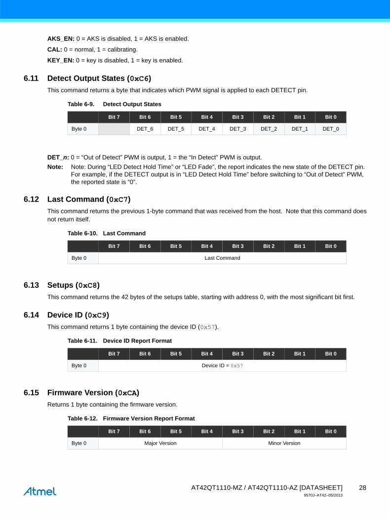
6.11 Detect Output States (0xC6)
This command returns a byte that indicates which PWM signal is applied to each DETECT pin.
DET_n: 0 = “Out of Detect” PWM is output, 1 = the “In Detect” PWM is output.
Note: Note: During “LED Detect Hold Time” or “LED Fade”, the report indicates the new state of the DETECT pin. For example, if the DETECT output is in “LED Detect Hold Time” before switching to “Out of Detect” PWM, the reported state is “0”.
6.12 Last Command (0xC7)
This command returns the previous 1-byte command that was received from the host. Note that this command doesnot return itself.
6.13 Setups (0xC8)
This command returns the 42 bytes of the setups table, starting with address 0, with the most significant bit first.
6.14 Device ID (0xC9)
This command returns 1 byte containing the device ID (0x57).
6.15 Firmware Version (0xCA)
Returns 1 byte containing the firmware version.
Table 6-9. Detect Output States
Bit 7 Bit 6 Bit 5 Bit 4 Bit 3 Bit 2 Bit 1 Bit 0
Byte 0 DET_6 DET_5 DET_4 DET_3 DET_2 DET_1 DET_0
Table 6-10. Last Command
Bit 7 Bit 6 Bit 5 Bit 4 Bit 3 Bit 2 Bit 1 Bit 0
Byte 0 Last Command
Table 6-11. Device ID Report Format
Bit 7 Bit 6 Bit 5 Bit 4 Bit 3 Bit 2 Bit 1 Bit 0
Byte 0 Device ID = 0x57
Table 6-12. Firmware Version Report Format
Bit 7 Bit 6 Bit 5 Bit 4 Bit 3 Bit 2 Bit 1 Bit 0
Byte 0 Major Version Minor Version
28AT42QT1110-MZ / AT42QT1110-AZ [DATASHEET]9570J–AT42–05/2013
7. Setups and Status Information
7.1 Introduction
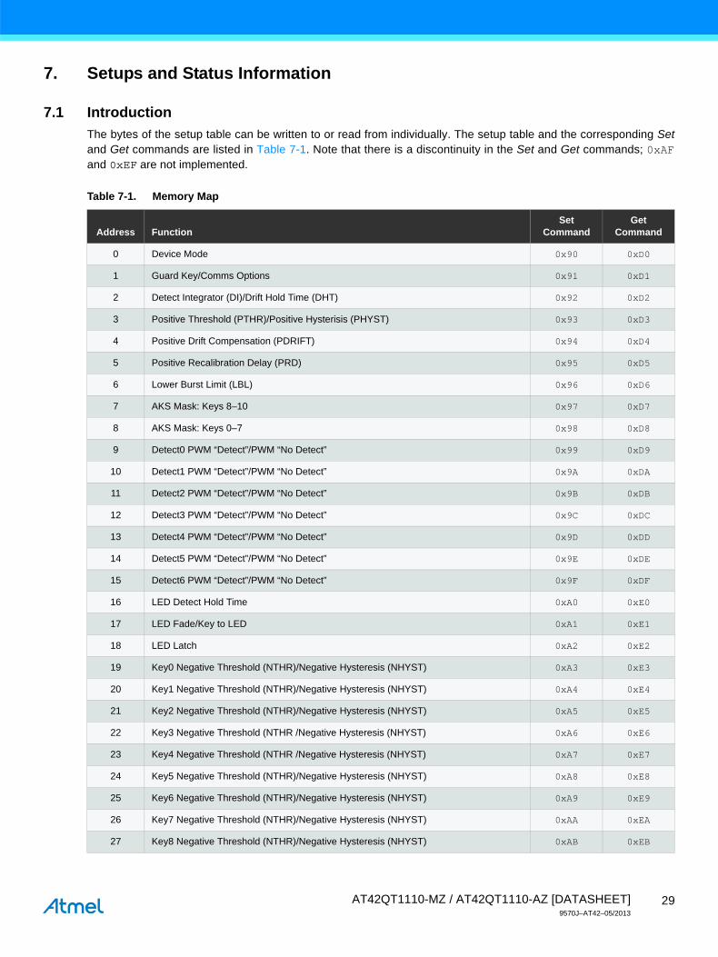
The bytes of the setup table can be written to or read from individually. The setup table and the corresponding Setand Get commands are listed in Table 7-1. Note that there is a discontinuity in the Set and Get commands; 0xAFand 0xEF are not implemented.
Table 7-1. Memory Map
Address FunctionSet
CommandGet
Command
0 Device Mode 0x90 0xD0
1 Guard Key/Comms Options 0x91 0xD1
2 Detect Integrator (DI)/Drift Hold Time (DHT) 0x92 0xD2
3 Positive Threshold (PTHR)/Positive Hysterisis (PHYST) 0x93 0xD3
4 Positive Drift Compensation (PDRIFT) 0x94 0xD4
5 Positive Recalibration Delay (PRD) 0x95 0xD5
6 Lower Burst Limit (LBL) 0x96 0xD6
7 AKS Mask: Keys 8–10 0x97 0xD7
8 AKS Mask: Keys 0–7 0x98 0xD8
9 Detect0 PWM “Detect”/PWM “No Detect” 0x99 0xD9
10 Detect1 PWM “Detect”/PWM “No Detect” 0x9A 0xDA
11 Detect2 PWM “Detect”/PWM “No Detect” 0x9B 0xDB
12 Detect3 PWM “Detect”/PWM “No Detect” 0x9C 0xDC
13 Detect4 PWM “Detect”/PWM “No Detect” 0x9D 0xDD
14 Detect5 PWM “Detect”/PWM “No Detect” 0x9E 0xDE
15 Detect6 PWM “Detect”/PWM “No Detect” 0x9F 0xDF
16 LED Detect Hold Time 0xA0 0xE0
17 LED Fade/Key to LED 0xA1 0xE1
18 LED Latch 0xA2 0xE2
19 Key0 Negative Threshold (NTHR)/Negative Hysteresis (NHYST) 0xA3 0xE3
20 Key1 Negative Threshold (NTHR)/Negative Hysteresis (NHYST) 0xA4 0xE4
21 Key2 Negative Threshold (NTHR)/Negative Hysteresis (NHYST) 0xA5 0xE5
22 Key3 Negative Threshold (NTHR /Negative Hysteresis (NHYST) 0xA6 0xE6
23 Key4 Negative Threshold (NTHR /Negative Hysteresis (NHYST) 0xA7 0xE7
24 Key5 Negative Threshold (NTHR)/Negative Hysteresis (NHYST) 0xA8 0xE8
25 Key6 Negative Threshold (NTHR)/Negative Hysteresis (NHYST) 0xA9 0xE9
26 Key7 Negative Threshold (NTHR)/Negative Hysteresis (NHYST) 0xAA 0xEA
27 Key8 Negative Threshold (NTHR)/Negative Hysteresis (NHYST) 0xAB 0xEB
29AT42QT1110-MZ / AT42QT1110-AZ [DATASHEET]9570J–AT42–05/2013

7.2 Setting Individual Settings
To set up an individual setup value, the host sends the command listed under the “Set Command” column in Table 7-1, followed by a byte of data.
For details of the communication flow, see Section 4.1 on page 11.
7.3 Setting All the Setups
The host can send all 42 bytes of setup data to the QT1110 as a block using the Send Setups command. SeeSection 5.2 on page 22 for details.
7.4 Address 0: Device Mode
The Device Mode controls the overall operation of the device: number of keys, acquisition method, timing and triggermechanism.
KEY_AC: selects the trigger source to start key acquisition; 0 = SYNC pin, 1 = timed.
MODE: selects 7-key or 11-key mode; 0 = default 7-key mode, 1 = 11-key mode.
SIGNAL: selects serial or parallel acquisition of keys signals; 0 = serial, 1 = parallel.
SYNC: selects the trigger type when SYNC Pin is selected as the trigger to start key acquisition.
28 Key9 Negative Threshold (NTHR)/Negative Hysteresis (NHYST) 0xAC 0xEC
29 Key10 Negative Threshold (NTHR)/Negative Hysteresis (NHYST) 0xAD 0xED
30 Extend Pulse Time 0xAE 0xEE
31 Key0 Negative Drift Compensation (NDRIFT)/Negative Recalibration Delay (NRD) 0xB0 0xF0
32 Key1 Negative Drift Compensation (NDRIFT)/Negative Recalibration Delay (NRD) 0xB1 0xF1
33 Key2 Negative Drift Compensation (NDRIFT)/Negative Recalibration Delay (NRD) 0xB2 0xF2
34 Key3 Negative Drift Compensation (NDRIFT)/Negative Recalibration Delay (NRD) 0xB3 0xF3
35 Key4 Negative Drift Compensation (NDRIFT)/Negative Recalibration Delay (NRD) 0xB4 0xF4
36 Key5 Negative Drift Compensation (NDRIFT)/Negative Recalibration Delay (NRD) 0xB5 0xF5
37 Key6 Negative Drift Compensation (NDRIFT)/Negative Recalibration Delay (NRD) 0xB6 0xF6
38 Key7 Negative Drift Compensation (NDRIFT)/Negative Recalibration Delay (NRD) 0xB7 0xF7
39 Key8 Negative Drift Compensation (NDRIFT)/Negative Recalibration Delay (NRD) 0xB8 0xF8
40 Key9 Negative Drift Compensation (NDRIFT)/Negative Recalibration Delay (NRD) 0xB9 0xF9
41 Key10 Negative Drift Compensation (NDRIFT)/Negative Recalibration Delay (NRD) 0xBA 0xFA
Table 7-1. Memory Map (Continued)
Address FunctionSet
CommandGet
Command
Table 7-2. Device Mode
Address Bit 7 Bit 6 Bit 5 Bit 4 Bit 3 Bit 2 Bit 1 Bit 0
0 KEY_AC MODE SIGNAL SYNC REPEAT_TIME
30AT42QT1110-MZ / AT42QT1110-AZ [DATASHEET]9570J–AT42–05/2013

0 = Level Acquisition starts when a 0 is read at the SYNC pin. If the pin is heldlow, the QT1110 operates in Free run mode (that is, it will not sleep inbetween acquisitions, but start again immediately).
1 = Edge Acquisition starts when a rising edge is detected at the SYNC pin.When acquisition and post-processing are completed, the device sleeps until another rising edge is detected at the SYNC pin.
REPEAT_TIME: selects the “repeat” time when “Timed” is selected as the trigger to start key acquisition. Thenumber entered is a multiple of 16 ms. If 0 is entered, the device will operate in a continuous free run mode; that is,the QT1110 will not sleep after its cycle is completed but will begin the next key acquisition cycle immediately.
Default KEY_AC value: 1 (timed)Default MODE value: 0 (7-key mode)Default SIGNAL value: 1 (parallel)Default SYNC value: 1 (edge)Default REPEAT_TIME value: 2 (32 ms cycle)
7.5 Address 1: Guard Key/Comms Options
GUARD_KEY: specifies the key (0 to 10) to be used as a guard channel (see Section 2.3 on page 8) .
GD_EN: enables the use of a guard key; 0 = disable, 1 = enable.
SPI_EN: enables the Quick SPI interface; 0 = disable, 1 = enable.
See Section 4.1.6 on page 16 for details of the Quick SPI Mode report.
To exit this mode (and clear the SPI_EN bit), the command 0x36 should be sent. To save the settings to EEPROMand make Quick SPI mode active on startup, send the Store to EEPROM command (0x0A). Any other data sent isignored in Quick SPI mode.
CHG: the CHANGE pin mode (see Section 4.5 on page 18):
0 = Data mode. In this mode the CHANGE pin is asserted to indicate unread data.
1 = Touch mode. In this mode the CHANGE pin is asserted when a key is being touchedor is in detect.
CRC: enables or disables CRC; 0 = disable, 1 = enable. When this option is enabled, each data exchange musthave a CRC byte appended.
When report or setup data is being returned by the QT1110, a 1-byte checksum is returned. The host should confirmthat this checksum is correct and, if not, should request the report again.
Where data is being sent by the host, a 1-byte CRC should be sent. The QT1110 returns the expected CRC byte inthe same transaction the CRC byte is sent. In this way, the host can immediately determine whether the setup databytes were received correctly.
Default GUARD_KEY value: 0 (Key 0)Default GD_EN value: 0 (disabled)Default CHG value: 0 (data mode)Default CRC value: 0 (disabled)
Table 7-3. Guard Key/Comms Options
Address Bit 7 Bit 6 Bit 5 Bit 4 Bit 3 Bit 2 Bit 1 Bit 0
1 GUARD_KEY GD_EN SPI_EN CHG CRC
31AT42QT1110-MZ / AT42QT1110-AZ [DATASHEET]9570J–AT42–05/2013

7.6 Address 2: Detect Integrator Limit (DIL)/Drift Hold Time (DHT)
DIL: the detection integrator (DI) limit. To suppress false detections caused by spurious events like electrical noise,the device incorporates a DI counter mechanism. A per-key counter is incremented each time the channel hasexceeded its threshold and stayed there for a number of acquisitions in succession, without going below thethreshold level. When this counter reaches a preset limit the channel is finally declared to be touched. If on anyacquisition the delta is not seen to exceed the threshold level, the counter is cleared and the process has to startfrom the beginning.
Note: A setting of 0 for DI is invalid; the valid range is 1 to 15.
DHT: the drift hold time. After a key-touch has been removed, the QT1110 pauses in the implementation of its “Drift”compensation for a time. After this time has expired, drift compensation continues as normal. The Drift Hold Time isa multiple of 160 ms, providing options from 0 to 2400 ms.
Default DIL value: 3Default DHT value: 8 (1280 ms)
7.7 Address 3: Positive Threshold (PTHR)/Positive Hysteresis (PHYST)
PTHR: the positive threshold for the signal. If a key signal is significantly higher than the reference signal, thistypically indicates that the calibration data is no longer valid. In other words, some factor has changed since thecalibration was carried out, thus rendering it invalid. Generally this is compensated for by the drift, but the greater thedifference the longer this will take. In order to speed up this correction, the positive threshold is used: if the positivethreshold is exceeded, the QT1110 (that is, all keys) is recalibrated.
PHYST: positive hysteresis. This setting provides a greater degree of control over the implementation of the positivethreshold recalibration. The positive hysteresis operates as a “modifier” for the positive threshold. When a key signalis detected as being over the positive threshold, the positive threshold is reduced by a factor corresponding to thepositive hysteresis so that the key will not go in and out of positive detection when the signal is on the borderlinebetween drift-compensation of a positive error or recalibration.
The settings for positive hysteresis are:
00 = No change to positive threshold
01 = 12.5% reduction in positive-detect threshold
10 = 25% reduction in positive-detect threshold
11 = 37.5% reduction in positive-detect threshold
Default PTHR value: 4 (4 counts above reference)Default PHYST value: 2 (25% positive hysteresis)
Table 7-4. Detect Integrator/Drift Hold Time
Address Bit 7 Bit 6 Bit 5 Bit 4 Bit 3 Bit 2 Bit 1 Bit 0
2 DIL DHT
Table 7-5. Positive Threshold (THR)/Positive Hystereis (HYST)
Address Bit 7 Bit 6 Bit 5 Bit 4 Bit 3 Bit 2 Bit 1 Bit 0
3 PTHR PHYST
32AT42QT1110-MZ / AT42QT1110-AZ [DATASHEET]9570J–AT42–05/2013

7.8 Address 4: Positive Drift Compensation (PDRIFT)
When changing ambient conditions cause a change in the key signal, the QT1110 will compensate through its driftfunctions. Positive Drift refers to the case where the signal for a key is greater than the reference.
Drift compensation occurs at a rate of 1 count per drift compensation period.
PDRIFT: the drift compensation period, in multiples of 160 ms. The valid range is 0 to 127, where 0 disables positivedrift compensation.
Note: Drift compensation timing is paused while Drift Hold is activated, and continued when Drift Hold has timed out.
Default value: 6 (960 ms)
7.9 Address 5: Positive Recalibration Delay (PRD)
If a key signal is determined to be above the positive threshold, the QT1110 will wait for this delay and confirm thatthe error condition is still present before initiating a recalibration.
PRD: the positive recalibration delay, in multiples of 160 ms.
Note: All keys are recalibrated in the case of a positive recalibration.
Default value: 6 (960 ms)
7.10 Address 6: Lower Burst Limit (LBL)
Normal QTouch signals are in the range of 100 to 1000 counts for each key. The lower burst limit determines theminimum signal that is considered as a valid acquisition. If the count is lower than the lower burst limit, it isconsidered not to be valid and the key is set to an Error state.
Note: Where a key has a signal of less than the LBL, a detection is not reported on that key.
Default value: 18
Table 7-6. Positive Drift Compensation
Address Bit 7 Bit 6 Bit 5 Bit 4 Bit 3 Bit 2 Bit 1 Bit 0
4 0 PDRIFT
Table 7-7. Positive Recalibration Delay
Address Bit 7 Bit 6 Bit 5 Bit 4 Bit 3 Bit 2 Bit 1 Bit 0
5 PRD
Table 7-8. Lower Burst Limit
Address Bit 7 Bit 6 Bit 5 Bit 4 Bit 3 Bit 2 Bit 1 Bit 0
6 LBL
33AT42QT1110-MZ / AT42QT1110-AZ [DATASHEET]9570J–AT42–05/2013
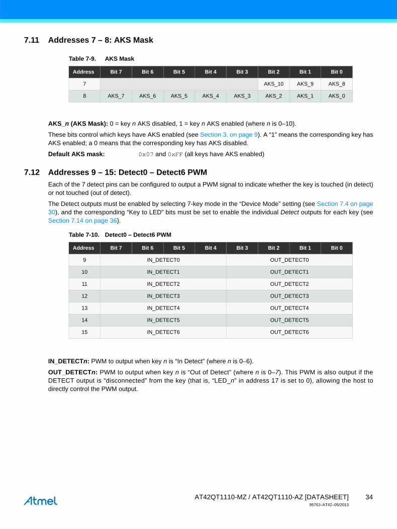
7.11 Addresses 7 – 8: AKS Mask
AKS_n (AKS Mask): 0 = key n AKS disabled, 1 = key n AKS enabled (where n is 0–10).
These bits control which keys have AKS enabled (see Section 3. on page 9). A “1” means the corresponding key hasAKS enabled; a 0 means that the corresponding key has AKS disabled.
Default AKS mask: 0x07 and 0xFF (all keys have AKS enabled)
7.12 Addresses 9 – 15: Detect0 – Detect6 PWM
Each of the 7 detect pins can be configured to output a PWM signal to indicate whether the key is touched (in detect)or not touched (out of detect).
The Detect outputs must be enabled by selecting 7-key mode in the “Device Mode” setting (see Section 7.4 on page30), and the corresponding “Key to LED” bits must be set to enable the individual Detect outputs for each key (seeSection 7.14 on page 36).
IN_DETECTn: PWM to output when key n is “In Detect” (where n is 0–6).
OUT_DETECTn: PWM to output when key n is “Out of Detect” (where n is 0–7). This PWM is also output if theDETECT output is “disconnected” from the key (that is, “LED_n” in address 17 is set to 0), allowing the host todirectly control the PWM output.
Table 7-9. AKS Mask
Address Bit 7 Bit 6 Bit 5 Bit 4 Bit 3 Bit 2 Bit 1 Bit 0
7 AKS_10 AKS_9 AKS_8
8 AKS_7 AKS_6 AKS_5 AKS_4 AKS_3 AKS_2 AKS_1 AKS_0
Table 7-10. Detect0 – Detect6 PWM
Address Bit 7 Bit 6 Bit 5 Bit 4 Bit 3 Bit 2 Bit 1 Bit 0
9 IN_DETECT0 OUT_DETECT0
10 IN_DETECT1 OUT_DETECT1
11 IN_DETECT2 OUT_DETECT2
12 IN_DETECT3 OUT_DETECT3
13 IN_DETECT4 OUT_DETECT4
14 IN_DETECT5 OUT_DETECT5
15 IN_DETECT6 OUT_DETECT6
34AT42QT1110-MZ / AT42QT1110-AZ [DATASHEET]9570J–AT42–05/2013

The values for the “IN_DETECTn” and “OUT_DETECTn” nibbles are listed in Table 7-11.
Default IN_DETECTn value: 8 (100% PWM – on)Default OUT_DETECTn value: 0 (0% PWM – off)
7.13 Address 16: LED Detect Hold Time
When a key is touched, if the “Detect” outputs and “Key to LED” options are enabled (see Section 7.12 and Section7.14), the corresponding “Detect” pin will output its “In-Detect” PWM signal.
After the key touch is removed, the “Detect” output can be held at the “In-Detect” PWM signal for a time beforereturning to the “Out of Detect” PWM signal. This allows a reasonable length of time for an LED to be illuminated.The length of this time is controlled by the LED Detect Hold Time. Valid values are in multiples of 16 ms.
Default value: 0 (0 ms)
Table 7-11. PWM Values
Value Meaning
0 0%
1 12.5%
2 25%
3 37.5%
4 50%
5 62.5%
6 75%
7 87.5%
8 100%
Table 7-12. LED Detect Hold Time
Address Bit 7 Bit 6 Bit 5 Bit 4 Bit 3 Bit 2 Bit 1 Bit 0
16 LED_DETECT_HOLD_TIME
35AT42QT1110-MZ / AT42QT1110-AZ [DATASHEET]9570J–AT42–05/2013

7.14 Address 17: LED Fade/Key to LED
FADE: enables/disables fading for all LEDs. This is a global setting; either all LEDs fade, or none of them.
0 = disable (no fade).
1 = enable fading on and off.
LED_n: activates the LED output for the corresponding key output DETECTn (where n is 0–6).
1 = enables the “Detect” output to follow the status of the corresponding key.
0 = disable this function, in which case the “Detect” pin will always output its “Out of Detect” PWM (see Section 7.12on page 34).
Default FADE value: 0 (disabled)Default LED_n value: 1 (enabled)
7.15 Address 18: LED Latch
LATCH_n: enables/disables latching of the LED for the corresponding key output DETECTn (where n is 0–6).
1 = enables latching. When latching is enabled for a given LED, the LED toggles its state each time the key istouched.
0 = disables latching.
Note that bit 7 is reserved and should be set to zero.
Default LATCH_n value: 0x00 (latch disabled)
7.16 Addresses 19 – 29: Negative Threshold (NTHR) / Negative Hysteresis (NHYST)
Table 7-13. LED Fade/Key to LED
Address Bit 7 Bit 6 Bit 5 Bit 4 Bit 3 Bit 2 Bit 1 Bit 0
17 FADE LED_6 LED_5 LED_4 LED_3 LED_2 LED_1 LED_0
Table 7-14. LED Latch
Address Bit 7 Bit 6 Bit 5 Bit 4 Bit 3 Bit 2 Bit 1 Bit 0
18 0 LATCH_6 LATCH_5 LATCH_4 LATCH_3 LATCH_2 LATCH_1 LATCH_0
Table 7-15. Negative Threshold / Negative Hysteresis
Address Bit 7 Bit 6 Bit 5 Bit 4 Bit 3 Bit 2 Bit 1 Bit 0
19 KEY_0_NTHR KEY_0_NHSYT
20 KEY_1_NTHR KEY_1_NHSYT
21 KEY_2_NTHR KEY_2_NHSYT
22 KEY_3_NTHR KEY_3_NHSYT
23 KEY_4_NTHR KEY_4_NHSYT
24 KEY_5_NTHR KEY_5_NHSYT
25 KEY_6_NTHR KEY_6_NHSYT
36AT42QT1110-MZ / AT42QT1110-AZ [DATASHEET]9570J–AT42–05/2013

KEY_n_NTHR: the negative threshold for key n (where n is 0–10).
The negative threshold determines how much the signal must fall (compared to the reference) before a key isconsidered to be “In Detect”. This level will generally need to be tuned individually for each key. To disable anindividual key, set the threshold for that key to 0.
KEY_n_NHYST: the negative hysteresis applied to key n detection threshold (where n is0 – 10).
Negative Hysteresis operates as a “modifier” for the negative threshold in order to provide a greater degree of controlover the detection of a “Touch”. When a key signal is first detected as being under the negative threshold, thethreshold is reduced by a factor corresponding to the selected negative hysteresis. This means that the key will notgo in and out of detection when the signal is on the borderline between drift-compensation or touch detection.
The settings for negative hysteresis are:
00 No change to negative threshold
01 12.5% reduction in negative threshold
10 25% reduction in negative threshold
11 37.5% reduction in negative threshold
Default KEY_n_NTHR value: 10 countsDefault KEY_n_NHYST value: 2 (25 percent)
7.17 Address 30: Extend Pulse Time
HIGH_TIME: Number of µs to extend the high pulse time.
LOW_TIME: Number of µs to extend the low pulse time.
26 KEY_7_NTHR KEY_7_NHSYT
27 KEY_8_NTHR KEY_8_NHSYT
28 KEY_9_NTHR KEY_9_NHSYT
29 KEY_10_NTHR KEY_10_NHSYT
Table 7-15. Negative Threshold / Negative Hysteresis (Continued)
Address Bit 7 Bit 6 Bit 5 Bit 4 Bit 3 Bit 2 Bit 1 Bit 0
Table 7-16. Extend Pulse Time
Address Bit 7 Bit 6 Bit 5 Bit 4 Bit 3 Bit 2 Bit 1 Bit 0
30 HIGH_TIME LOW_TIME
37AT42QT1110-MZ / AT42QT1110-AZ [DATASHEET]9570J–AT42–05/2013

7.18 Addresses 31 – 41: Negative Drift Compensation (NDRIFT) / Negative Recalibration Delay (NRD)
KEY_n_NDRIFT: the negative drift compensation for key n (where n is 0–10).
When changing ambient conditions cause a change in the key signal, the QT1110 will compensate through its driftfunctions. “Negative Drift” refers to the case where the signal for a key is lower than the reference. Driftcompensation occurs at a rate of 1 count per drift compensation period. The entered number is a multiple of 320 ms.
Note that as a key touch, or an approaching touch, naturally causes a negative change in the signal, negative driftshould be carried out at a much slower rate than positive drift. Otherwise, a slowly approaching finger will not causea touch detection, as the falling signal could be compensated through the negative drift mechanism.
Note: Drift compensation timing is paused while Drift Hold is activated, and continues when Drift Hold has timed out.
KEY_n_NRD: the negative recalibration delay for key n (where n is 0 – 10).
In order to avoid a situation where a key remains “stuck” in detect due to, for example, changing environmentalconditions, the “Negative Recalibration Delay” sets an upper limit on how long a key can remain “touched”. Whenthis time is exceeded, the QT1110 (that is, all keys) is recalibrated, taking this key (and any others which are indetect) out of detection. This delay is set in a multiple of 2560 ms.
Note: A setting of “0” disables the NRD Timeout.
Default KEY_n_NDRIFT value: 7 (2240 ms)Default KEY_n_NRD value: 10 (25.6 s)
Table 7-17. Negative Drift Compensation / Negative Recalibration Delay
Address Bit 7 Bit 6 Bit 5 Bit 4 Bit 3 Bit 2 Bit 1 Bit 0
31 KEY_0_NDRIFT KEY_0_NRD
32 KEY_1_NDRIFT KEY_1_NRD
33 KEY_2_NDRIFT KEY_2_NRD
34 KEY_3_NDRIFT KEY_3_NRD
35 KEY_4_NDRIFT KEY_4_NRD
36 KEY_5_NDRIFT KEY_5_NRD
37 KEY_6_NDRIFT KEY_6_NRD
38 KEY_7_NDRIFT KEY_7_NRD
39 KEY_8_NDRIFT KEY_8_NRD
40 KEY_9_NDRIFT KEY_9_NRD
41 KEY_10_NDRIFT KEY_10_NRD
38AT42QT1110-MZ / AT42QT1110-AZ [DATASHEET]9570J–AT42–05/2013

8. Specifications
8.1 Absolute Maximum Specifications
8.2 Recommended Operating Conditions
8.3 DC Specifications
Vdd –0.5 V to +6 V
Max continuous pin current, any control or drive pin ±10 mA
Voltage forced onto any pin –1.0 V to (Vdd + 0.5) V
EEPROM setups maximum writes 100,000 write cycles
CAUTION: Stresses beyond those listed under Absolute Maximum Specifications may cause permanent damage to the device. This is a stress rating only and functional operation of the device at these or other conditions beyond those indicated in the operational sections of this specification is not implied. Exposure to absolute maximum specification conditions for extended periods may affect device reliability
Operating temperature –40°C to +125°C
Storage temperature –65°C to +150°C
Vdd 3 V to 5.5 V
Supply ripple + noise ±20 mV
Cx transverse load capacitance per key 2 pF to 20 pF
Vdd = 5.0V, Cs = 4.7 nF, Rs = 1 M, Ta = recommended range, unless otherwise noted
Parameter Description Min Typ Max Units Notes
Iddr Average supply current, running – –12 at 5 V8 at 3 V
mAFor typical values see Section 8.8
Vil Low input logic level –0.5V – 0.3 × Vdd V
Vih High input logic level 0.6 × Vdd Vdd Vdd + 0.5 V
Vol Low output voltage 0 – 0.7 V 10 mA sink current
Voh High output voltage 0.8 × Vdd – Vdd V 10 mA source current
Iil Input leakage current – <0.05 1 µA
Rrst Internal RST pull-up resistor 30 – 60 k
39AT42QT1110-MZ / AT42QT1110-AZ [DATASHEET]9570J–AT42–05/2013
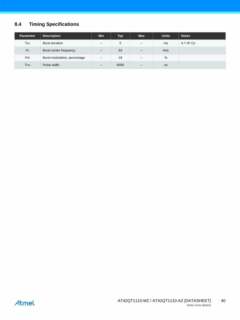
8.4 Timing Specifications
Parameter Description Min Typ Max Units Notes
TBS Burst duration – 5 – ms 4.7 nF Cs
Fc Burst center frequency – 53 – kHz
Fm Burst modulation, percentage – 18 – %
TPW Pulse width – 6000 – ns
40AT42QT1110-MZ / AT42QT1110-AZ [DATASHEET]9570J–AT42–05/2013

8.5 SPI Bus Specifications
8.5.1 General Specifications
8.5.2 Full SPI Mode
8.5.3 Quick SPI Mode
Parameter Specification
Address space 8-bit
Maximum clock rate 1.5 MHz
Minimum low clock period 333 ns
Minimum high clock period 333 ns
Clock idle High
Setup on Leading (falling) edge
Clock out on Trailing (rising) edge
SPI Enable delay (SS low to SCK low) 1 µs minimum
Parameter Specification
Minimum time between bytes 150 µs
Minimum time between communications
Generally 150 µs; longer delays required to implement some commands, as follows:
Send Setups: 150 µs after all setup bytes are returned
Calibrate All: 150 µs
Calibrate Key: 150 µs
Reset: 160 ms
Sleep: 150 µs after a low signal is applied to SS or CHANGE to wake the device
Store to EEPROM: 200 ms
Restore from EEPROM: 150 ms
Erase EEPROM: 50 ms
Recover EEPROM: 50 ms
Parameter Specification
Minimum time between bytes 50 µs
Minimum time between communications
Generally 50 µs, except for the following:
Store to EEPROM: 200 ms
Switch to Full SPI: 150 µs
41AT42QT1110-MZ / AT42QT1110-AZ [DATASHEET]9570J–AT42–05/2013
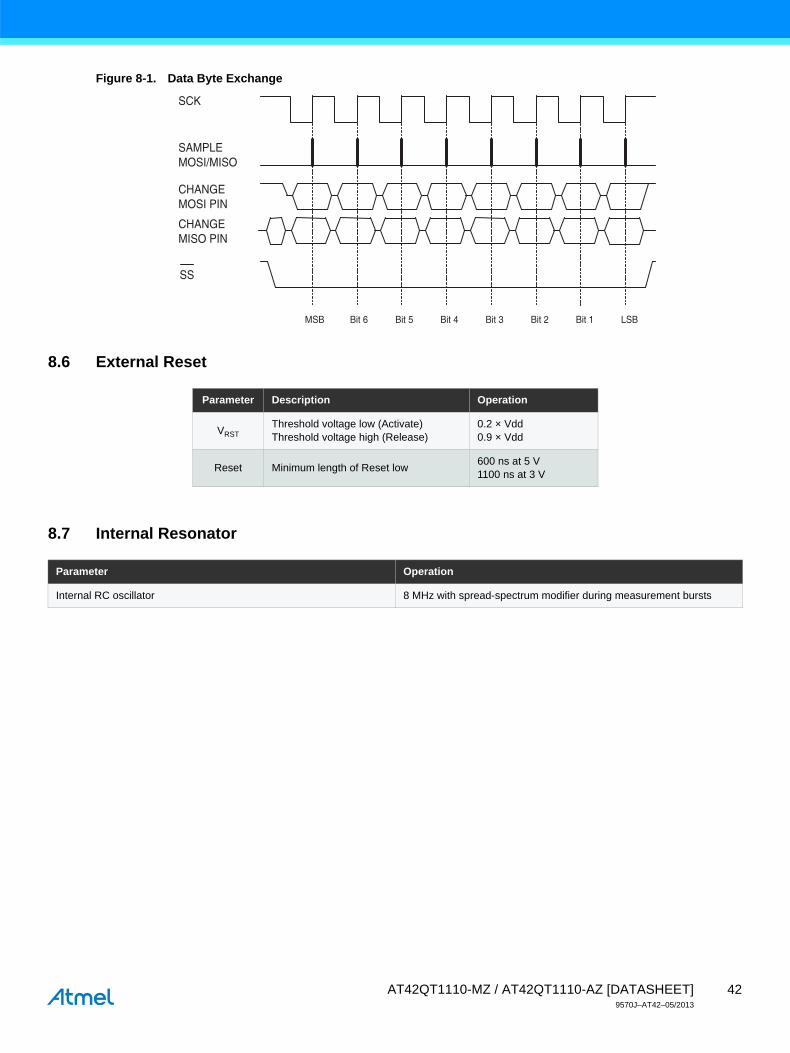
Figure 8-1. Data Byte Exchange
8.6 External Reset
8.7 Internal Resonator
SAMPLEMOSI/MISO
CHANGE MOSI PIN
CHANGEMISO PIN
SCK
SS
MSB Bit 6 Bit 5 Bit 4 Bit 3 Bit 2 Bit 1 LSB
Parameter Description Operation
VRSTThreshold voltage low (Activate) Threshold voltage high (Release)
0.2 × Vdd0.9 × Vdd
Reset Minimum length of Reset low600 ns at 5 V1100 ns at 3 V
Parameter Operation
Internal RC oscillator 8 MHz with spread-spectrum modifier during measurement bursts
42AT42QT1110-MZ / AT42QT1110-AZ [DATASHEET]9570J–AT42–05/2013

8.8 Power Consumption
7-key Parallel 7-key Serial 11-key Parallel 11-key Serial11-key Serial, 1 key enabled
Vdd (V) Cycle Time
Actual Cycle Time
(ms) Idd (µA)
Actual Cycle Time
(ms) Idd (µA)
Actual Cycle Time
(ms) Idd (µA)
Actual Cycle Time
(ms) Idd (µA)
Actual Cycle Time
(ms) Idd (µA)
4.7 nF Cs Capacitors
3.0
0 (Free Run) 13.2 2470 26.6 2350 15.3 2385 37.4 2420 2.15 2107
1 (16 ms Nominal) 17.2 2180 26.6 2350 17.3 2182 37.4 2420 16.5 950
2 (32 ms Nominal) 33.6 1470 34.4 1950 33.8 1435 37.4 2420 33 739
4 (64 ms Nominal) 66.4 1010 67.2 1325 66.4 1045 68.4 1587 66 691
8 (128 ms Nominal) 132 840 133 1025 132 840 134 1120 132 668
15 (240 ms Nominal) 248 815 250 850 250 810 250 1008 248 656
5.0
0 (Free Run) 15.1 5530 30.2 5405 17.3 5674 43.6 5425 2.15 4860
1 (16 ms Nominal) 17.2 5290 30.2 5405 17.3 5674 43.6 5425 16.3 2965
2 (32 ms Nominal) 33.4 4210 34.4 5350 33.6 4013 43.6 5425 32.6 2400
4 (64 ms Nominal) 65.6 3120 66.8 4015 65.6 3240 67.6 4130 64.8 2248
8 (128 ms Nominal) 130 2705 132 3225 130 2840 132 3530 129 2206
15 (240 ms Nominal) 244 2440 244 3035 246 2465 245 3015 244 2163
10 nF Cs Capacitors
3.0
0 (Free Run) 24.2 2375 48.4 2430 24.2 2434 63.6 2416 8.6 2130
1 (16 ms Nominal) 24.2 2375 48.4 2430 24.2 2434 63.6 2416 16.7 1422
2 (32 ms Nominal) 34.4 1860 48.4 2430 34 1945 63.6 2416 33 1065
4 (64 ms Nominal) 66.8 1285 68.4 1910 66.4 1290 69.6 2260 65 848
8 (128 ms Nominal) 131 995 133 1320 132 980 134 1485 130 766
15 (240 ms Nominal) 246 845 248 1030 246 824 248 1080 243 708
5.0
0 (Free Run) 26 5810 56.4 5510 28 5675 73.6 5596 8.6 5145
1 (16 ms Nominal) 26 5810 56.4 5510 28 5675 73.6 5596 16.6 3990
2 (32 ms Nominal) 34 5170 56.4 5510 34 5196 73.6 5596 32.6 3160
4 (64 ms Nominal) 66 3990 67.6 5120 66.4 3780 73.6 5596 64.8 2690
8 (128 ms Nominal) 131 3290 132 3850 130 2910 133 4055 129 2310
15 (240 ms Nominal) 244 2950 244 3310 242 2675 246 3170 241 2270
Note: These values are for reference only; values are untested.
43AT42QT1110-MZ / AT42QT1110-AZ [DATASHEET]9570J–AT42–05/2013

8.9 Mechanical Dimensions
8.9.1 AT42QT1110-MZ – 32-pin 5 x 5 mm QFN
��������� �� ������ ���
������ ��� �� ����� ��������� ���� �� ���� ������ � �!"��
�������
#$%&'�
(&�&��'� �� ����$���)*�+�����,��-�!�'���.! ����/*�00���"
�$��$#��1�&#'1$#',2�����3��� �.���4� /
�1# #$� ��5 #$%&
� �� )"6)� )"67� �"))
� ��� )"))� )")�� )")7
� ��� 8� )"97� )":)
� ��� � )"�)�;&+
� <� )"�6 )"�� )"�)
� �� �
� ��� �
� ��� �"=7 �"�) �"�7
>"=) 7")) 7"�)
>":) >":7 >"6)
>":) >":7 >"6)
>"=) 7")) 7"�)
&
� &��
� &�� �"=7 �"�) �"�7
� �� � )"7)�?'�
��@� )"�)� )">)� )"7)
���� 8� 8� )"9)
���� 8� 8� ��A �
)"�) 8 8
�
B
'��?$@
��
�
&� &
�<
����
����
��
&�
)")6 �
@
���
�
�
����
%$��1&C
'1�&�1&C
?$%%$��1&C
������1�
����D��#���E,)"�)�;/
B
B
������*����� �*�7F7F�")� �?��G*�@� ������E)"7) *��"�) ��&F������� �*���G�%E��*+��������E�H. ��+! ��#��@� ��� �� ���,H+#/
44AT42QT1110-MZ / AT42QT1110-AZ [DATASHEET]9570J–AT42–05/2013

8.9.2 AT42QT1110-AZ – 32-pin 7 x 7 mm TQFP
��������� �� ������ ���
��� ��2%� �� ����� ��������� ���� �� ���� ������ � �!"��
�������
#������ �����"���%E���� �� ������3�� �����(&�&����3��������'�)�9*� �� ������?�"�� �����������������"����� ����������� ���&������������!.��� �!�������.����"���!!�� <!��� � ����������������������.��������)"�7� ���������"��� ����������� ���&�� ��� F� . �� � ������������������! �����<��G���I���� �����������!.����� �!�� �� ��E"� �����������������"���@� �����! � ���G����)"�)� � F� . "
� �� 8� 8� �"�)
� ��� )")7� 8� )"�7
� ��� �)"=7� �"))� �")7� ����������
� �� 6":7� ="))� ="�7
� ��� 9"=)� :"))� :"�)� #�����
� &� 6":7� ="))� ="�7
� &�� 9"=)� :"))� :"�)� #�����
� <������������)"�)� 8� )">7
� �� )")=� 8� )"�)
� @� )">7� 8� �)":7
� �� � )"6)�%��
�$��$#��1�&#'1$#',2�����3��� �.���4� /
'��?$@ �1# #$� ��5 #$%&
)AJ:A
@
�
�� �� �
?$%%$��1&C
'1�&�1&C
%$��1&C
&�
�
�
��
&<
���*����!� ��:")�F�:")F�")� �?��G*�)"6)� �@� ������E*�%E������3�!���! �����H. ��+! ��� �� ���,%H+�/
45AT42QT1110-MZ / AT42QT1110-AZ [DATASHEET]9570J–AT42–05/2013

8.10 Marking
8.10.1 AT42QT1110-MZ – 32-pin 5 x 5 mm QFN
8.10.2 AT42QT1110-AZ – 32-pin 7 x 7 mm TQFP
1
32Pin 1 ID
Abbreviation ofPart Number:AT42QT1110-MZ
Code Revision:4.5, Released
Datecode/Lot Number
ATMEL
MZ 4R5QT1110
Lot numberDate code Country Code
1
32
Abbreviation ofPart Number:AT42QT1110-AZ
Pin 1 ID
Code Revision:4.5, Released
Datecode/Lot Number
QT1110AZ45ATMEL
Date Code Lot Number
46AT42QT1110-MZ / AT42QT1110-AZ [DATASHEET]9570J–AT42–05/2013

8.11 Part Number
8.12 Moisture Sensitivity Level (MSL)
Part Number Description
AT42QT1110-MZ 32-pin 5 x 5 mm QFN RoHS compliant (-40°C to +125°C)
AT42QT1110-AZ 32-pin 7 x 7 mm TQFP RoHS compliant (-40°C to +125°C)
MSL Rating Peak Body Temperature Specifications
MSL3 260oC IPC/JEDEC J-STD-020
47AT42QT1110-MZ / AT42QT1110-AZ [DATASHEET]9570J–AT42–05/2013

Appendix A. CRC Calculation
If the use of a cyclic redundancy check (CRC) during data transmission is enabled, the host must generate a validCRC so that this can be correctly compared to the corresponding CRC generated by the QT1110. This appendixgives example C code to show how the CRC can be generated by the host.
/*=======================================================================
unsigned char calc_crc(unsigned char crc, unsigned char data)
---------------------------------------------------------------------------
Purpose: Calculate CRC for data packets
Input : CRC, Data
Output : Updated CRC
Notes : -
=========================================================================*/
unsigned char calc_crc(unsigned char crc, unsigned char data)
{
unsigned char index;
unsigned char fb;
index = 8;
do
{
fb = (crc ^ data) & 0x01u;
data >>= 1u;
crc >>= 1u;
if(fb)
{
crc ^= 0x8c;
}
} while(--index);
return crc;
}
/* Example Calling Routine */
unsigned char calculate_config_checksum(void)
{
int i;
unsigned char CRC_val = 0;
unsigned char setup_data[42] =
{
0xB2, 0x00, 0x38, 0x12, 0x06, 0x06, 0x12, 0x07, 0xFF, 0x80,
0x80, 0x80, 0x80, 0x80, 0x80, 0x80, 0x32, 0xFF, 0x00, 0x29,
0x80, 0x80, 0x80, 0x80, 0x80, 0x80, 0x80, 0x80, 0x80, 0x80,
0X00, 0x7A, 0x7A, 0x7A, 0x7A, 0x7A, 0x7A, 0x7A, 0x7A, 0x7A,
0x7A, 0x7A
};
for(i = 0; i < sizeof(setup_data); i++)
{
CRC_val = calc_crc(CRC_val, setup_data[i]);
}
return(CRC_val);
}
48AT42QT1110-MZ / AT42QT1110-AZ [DATASHEET]9570J–AT42–05/2013

Revision History
Revision No. History
Revision A – November 2008 Initial Release
Revision B – December 2008 Updated for chip revision 2.1
Revision C – December 2008 Updated SPI specifications
Revision D – February 2009 Updated for chip revision 3.1
Revision E – April 2009 Updated for chip revision 3.2:
added self-test function
Revision F – July 2009 Updated for chip revision 4.3:
added Quick SPI mode
Revision G – October 2009
Updated specifications
Erratum note added concerning CRC calculations for chip revision 4.3
Revision H – February 2010 Updated for chip revision 4.4
CRC calculations updated
Revision I – March 2010 Updated for chip revision 4.5
Revision J – March 2013 General updates
Apply new template
49AT42QT1110-MZ / AT42QT1110-AZ [DATASHEET]9570J–AT42–05/2013

Atmel Corporation
1600 Technology Drive
San Jose, CA 95110
USA
Tel: (+1) (408) 441-0311
Fax: (+1) (408) 487-2600
www.atmel.com
Atmel Asia Limited
Unit 01-5 & 16, 19F
BEA Tower, Millennium City 5
418 Kwun Tong Roa
Kwun Tong, Kowloon
HONG KONG
Tel: (+852) 2245-6100
Fax: (+852) 2722-1369
Atmel München GmbH
Business Campus
Parkring 4
D-85748 Garching bei München
GERMANY
Tel: (+49) 89-31970-0
Fax: (+49) 89-3194621
Atmel Japan G.K.
16F Shin-Osaki Kangyo Bldg
1-6-4 Osaki, Shinagawa-ku
Tokyo 141-0032
JAPAN
Tel: (+81) (3) 6417-0300
Fax: (+81) (3) 6417-0370
© 2013 Atmel Corporation. All rights reserved. / Rev.: 9570J–AT42–05/2013
Disclaimer: The information in this document is provided in connection with Atmel products. No license, express or implied, by estoppel or otherwise, to any intellectual property right is granted by this document or in connection with the sale of Atmel products. EXCEPT AS SET FORTH IN THE ATMEL TERMS AND CONDITIONS OF SALES LOCATED ON THE ATMEL WEBSITE, ATMEL ASSUMES NO LIABILITY WHATSOEVER AND DISCLAIMS ANY EXPRESS, IMPLIED OR STATUTORY WARRANTY RELATING TO ITS PRODUCTS INCLUDING, BUT NOT LIMITED TO, THE IMPLIED WARRANTY OF MERCHANTABILITY, FITNESS FOR A PARTICULAR PURPOSE, OR NON-INFRINGEMENT. IN NO EVENT SHALL ATMEL BE LIABLE FOR ANY DIRECT, INDIRECT, CONSEQUENTIAL, PUNITIVE, SPECIAL OR INCIDENTAL DAMAGES (INCLUDING, WITHOUT LIMITATION, DAMAGES FOR LOSS AND PROFITS, BUSINESS INTERRUPTION, OR LOSS OF INFORMATION) ARISING OUT OF THE USE OR INABILITY TO USE THIS DOCUMENT, EVEN IF ATMEL HAS BEEN ADVISED OF THE POSSIBILITY OF SUCH DAMAGES. Atmel makes no representations or warranties with respect to the accuracy or completeness of the contents of this document and reserves the right to make changes to specifications and products descriptions at any time without notice. Atmel does not make any commitment to update the information contained herein. Unless specifically provided otherwise, Atmel products are not suitable for, and shall not be used in, automotive applications. Atmel products are not intended, authorized, or warranted for use as components in applications intended to support or sustain life.
Atmel®, Atmel logo and combinations thereof, QTouch®, Adjacent Key Suppression®, AKS®, and others are registered trademarks or trademarks of Atmel Corporation or its subsidiaries. Other terms and product names may be registered trademarks or trademarks of others.