atlas iii-v advanced material device modeling - silvaco
TRANSCRIPT
ATLAS
ATLAS III-V Advanced Material Device Modeling
Requirements for III-V Device Simulation
ATLAS III-V Advanced Material Device Modeling
Blaze as Part of a Complete Simulation Toolset
III-V Device Simulation maturity has conventionally lagged behind
silicon leading to many immature standalone tools with a low user
base
Users must ensure that the simulator they evaluate has all the
necessary components
Blaze shares many common components of the ATLAS
framework with the mature and heavily used silicon simulator,
S-Pisces
Blaze is able to take advantage of ATLAS improvements in numerics, core functionality and analysis capabilities from
Silicon users
All of the features of ATLAS are available to Blaze users
Blaze is completely integrated with TonyPlot, DeckBuild and
DevEdit. Blaze experiments can be run the Virtual Wafer Fab
- 3 -

ATLAS III-V Advanced Material Device Modeling
Blaze as Part of the ATLAS Framework
- 4 -

ATLAS III-V Advanced Material Device Modeling
The 10 Essential Components of III-V Device
Simulation
1 Energy Balance / Hydrodynamic Models
velocity overshoot effects critical for accurate current prediction
non-local impact ionization
2 Lattice Heating
III-V substrates are poor conductors
significant local heating affects terminal characteristics
3 Fully Coupled Non-Isothermal Energy Balance Model
Important to treat Energy balance and lattice heating effects together
- 5 -
ATLAS III-V Advanced Material Device Modeling
The 10 Essential Components of III-V Device
Simulation (cont.)
4 Quantum Mechanical Simulation
Schrodinger solver
quantum correction models
Bohm Quantum Potential
5 High Frequency Solutions
Direct AC solver for arbitrarily high frequencies
AC parameter extraction
extraction of s-, z-, y-, and h-parameters
Smith chart and polar plot output
FFT for large signal transients
6 Interface and Bulk Traps
effect on terminal characteristics is profound
must be available in DC, transient and AC
- 6 -

ATLAS III-V Advanced Material Device Modeling
The 10 Essential Components of III-V Device
Simulation (cont.)
7 Circuit Performance Simulation (MixedMode)
for devices with no accurate compact model
verification of newly developed compact models
8 Optoelectronic Capability (Luminous/Laser)
ray tracing algorithms
DC, AC, transient and spectral response for detectors
Helmholtz solver for edge emitting laser diodes and VCSELs
LED simulation
9 Speed and Convergence
flexible and automatic choice of numerical methods
- 7 -
ATLAS III-V Advanced Material Device Modeling
The 10 Essential Components of III-V Device
Simulation (cont.)
10 C-Interpreter for interactive model development
user defined band parameter equations
large selection of user defined models
mole fraction dependent material parameters
ideal for proprietary model development
- 8 -
Simulation of III-V Device with Blaze

ATLAS III-V Advanced Material Device Modeling
Blaze Applications
Devices:
HEMTs
HBTs
MESFETs
etc
DC Characterization
Transient Analysis
Breakdown Calculations
AC Analysis
S-Parameter Calculation
- 10 -
ATLAS III-V Advanced Material Device Modeling
Material Parameters and Models
Blaze uses currently available material and model coefficients
taken from published data and university partners
For some materials often very little literature information is
available, especially composition dependent parameters for
ternary compounds
Some parameters (e.g. band alignments) are process dependent
Tuning of material parameters is essential for accurate results
- 11 -
ATLAS III-V Advanced Material Device Modeling
Material Parameters and Models (cont.)
Blaze provides access to all defaults though the input language
and an ASCII default parameter file
The ability to incorporate user equations into Blaze for mole
fraction dependent parameters is an extremely important extra
flexibility offered by Blaze
The C-Interpreter allows users to enter model equations (or
lookup tables) as C language routines. These are interpreted by
Blaze at run-time. No compilers are required
With correct tuning of parameters the results are accurate and predictive
- 12 -
ATLAS III-V Advanced Material Device Modeling
Blaze Simulation Overview
As with any ATLAS input deck the following phases are
necessary:
Structure definition
Material and model specification
Numerical methods selection
Solution specification
Results Analysis
- 13 -
ATLAS III-V Advanced Material Device Modeling
Structure Creation
Three methods exist to create III-V device structures
Process simulation (Flash)
Internal ATLAS syntax
limited to rectangular structures
Standalone device editor (DevEdit)
GUI to define structure, doping and mesh
batch mode for experimentation
abrupt and graded mole fraction definition
non-rectangular regions supported
- 14 -

ATLAS III-V Advanced Material Device Modeling
Structure Creation Using DevEdit
- 15 -
ATLAS III-V Advanced Material Device Modeling
Material Specification for Typical Devices
MESFETs
Mobilities
Schottky Barrier Height
HFETs (PHEMTs)
Composition Fraction
Band Offset
Mobilities
Schottky Barrier Height
HBTs
Composition Fraction
Band Offset
Minority Carrier Lifetimes
Mobilities
- 16 -

ATLAS III-V Advanced Material Device Modeling
Model Specification
Different sets of models can be applied for different regions
Specify models on material-by-material basis
Concentration dependent mobilities (conmob) can be applied only
to the AlGaAs material system
It is recommended for AlGaAs and all other materials to specify low-field mobilities in the MATERIAL statement and then apply
field dependent mobility in the MODEL statement:
MODEL MATERIAL=GaAs CONMOB FLDMOB SRH OPTR BGN
MODEL MATERIAL=AlGaAs FLDMOB SRH OPTR
MODEL MATERIAL=InGaAs FLDMOB SRH
- 17 -

ATLAS III-V Advanced Material Device Modeling
Model Specification (cont.)
Use MODELS PRINT to check model and material parameters in
the run-time output
Use IMPACT SELB for impact ionization. The default parameters
are for GaAs only
- 18 -
ATLAS III-V Advanced Material Device Modeling
Model Specification (cont.)
Typical models
Carrier Statistics
Fermi-Dirac / Boltzmann
Band gap narrowing
Recombination
SRH / Consrh
Auger
Optical
Impact Ionization
Selberherr / Grants / Crowell-Sze
Local / Non-local
- 19 -
ATLAS III-V Advanced Material Device Modeling
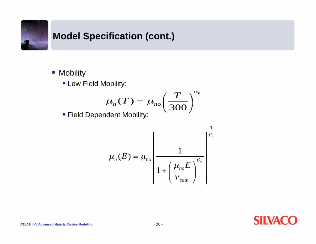
Model Specification (cont.)
Mobility
Low Field Mobility:
Field Dependent Mobility:
- 20 -
n
TT
nonμμ =
300)(
n
n
satn
no
non
E
E
μμμ
1
1
1)(
+
=
ATLAS III-V Advanced Material Device Modeling
Model Specification (cont.)
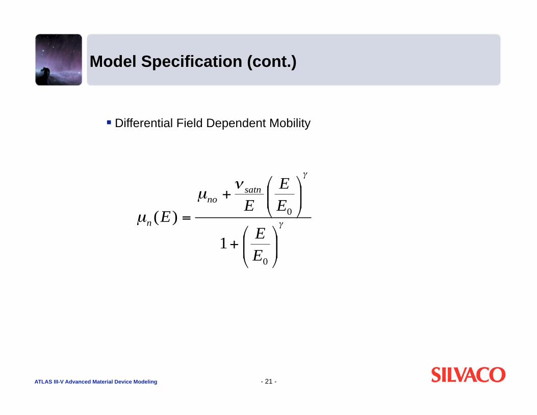
Differential Field Dependent Mobility
- 21 -
μ
μ
+
+
=
0
0
1
)(
E
E
E
E
EE
satn
no
n
ATLAS III-V Advanced Material Device Modeling
Models Specification (cont.)
Advanced Models
Thermionic emission model
This can be used to describe transport through abrupt heterojunctions
instead of the classical drift-diffusion model
It is the only physical model NOT activated using the
MODEL statement
for structures specified using ATLAS syntax use the REGION or INTERFACE
statement
for structures specified using DevEdit use the INTERFACE statement only
Traps
Bulk and Interface traps may be defined in the materials
Additional rate equation solved for each trap
- 22 -
ATLAS III-V Advanced Material Device Modeling
Model Specification (cont.)
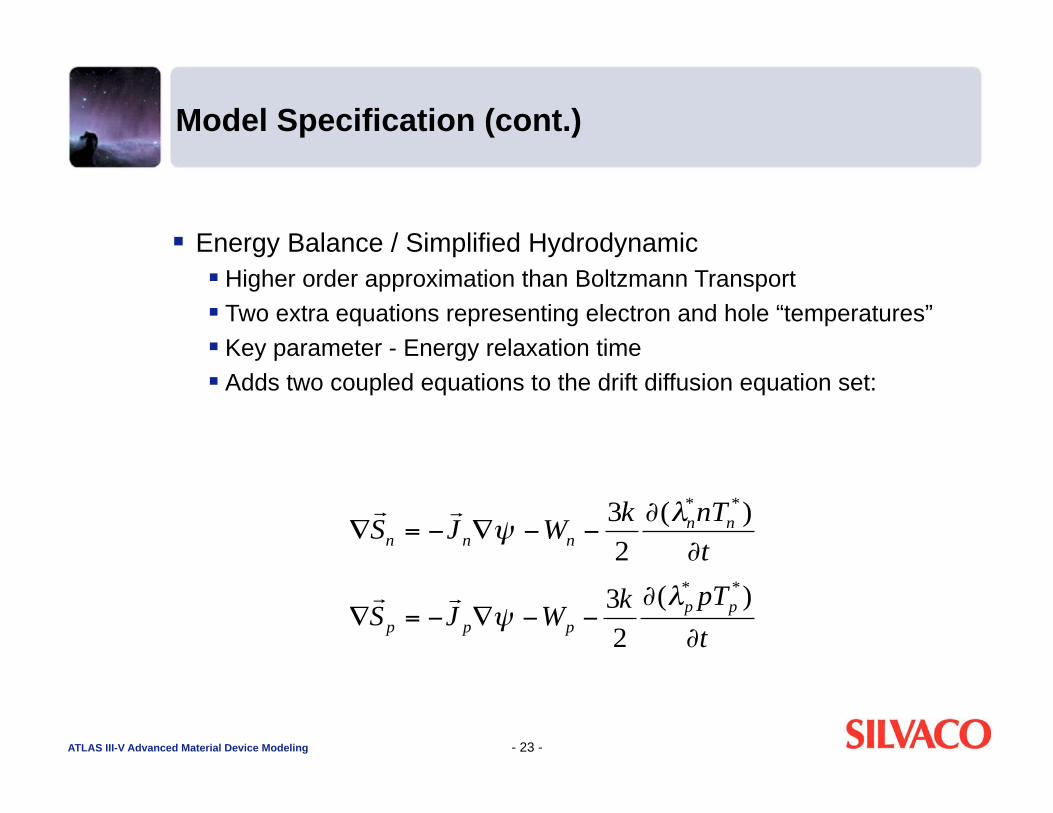
Energy Balance / Simplified Hydrodynamic
Higher order approximation than Boltzmann Transport
Two extra equations representing electron and hole “temperatures”
Key parameter - Energy relaxation time
Adds two coupled equations to the drift diffusion equation set:
- 23 -
t
nTkWJS
nn
nnn=
)(
2
3 **
t
pTkWJS
pp
ppp =)(
2
3**
ATLAS III-V Advanced Material Device Modeling
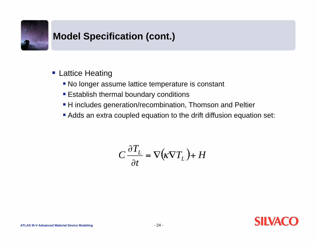
Model Specification (cont.)
Lattice Heating
No longer assume lattice temperature is constant
Establish thermal boundary conditions
H includes generation/recombination, Thomson and Peltier
Adds an extra coupled equation to the drift diffusion equation set:
- 24 -
( ) HTt
TC
L
L +=
ATLAS III-V Advanced Material Device Modeling
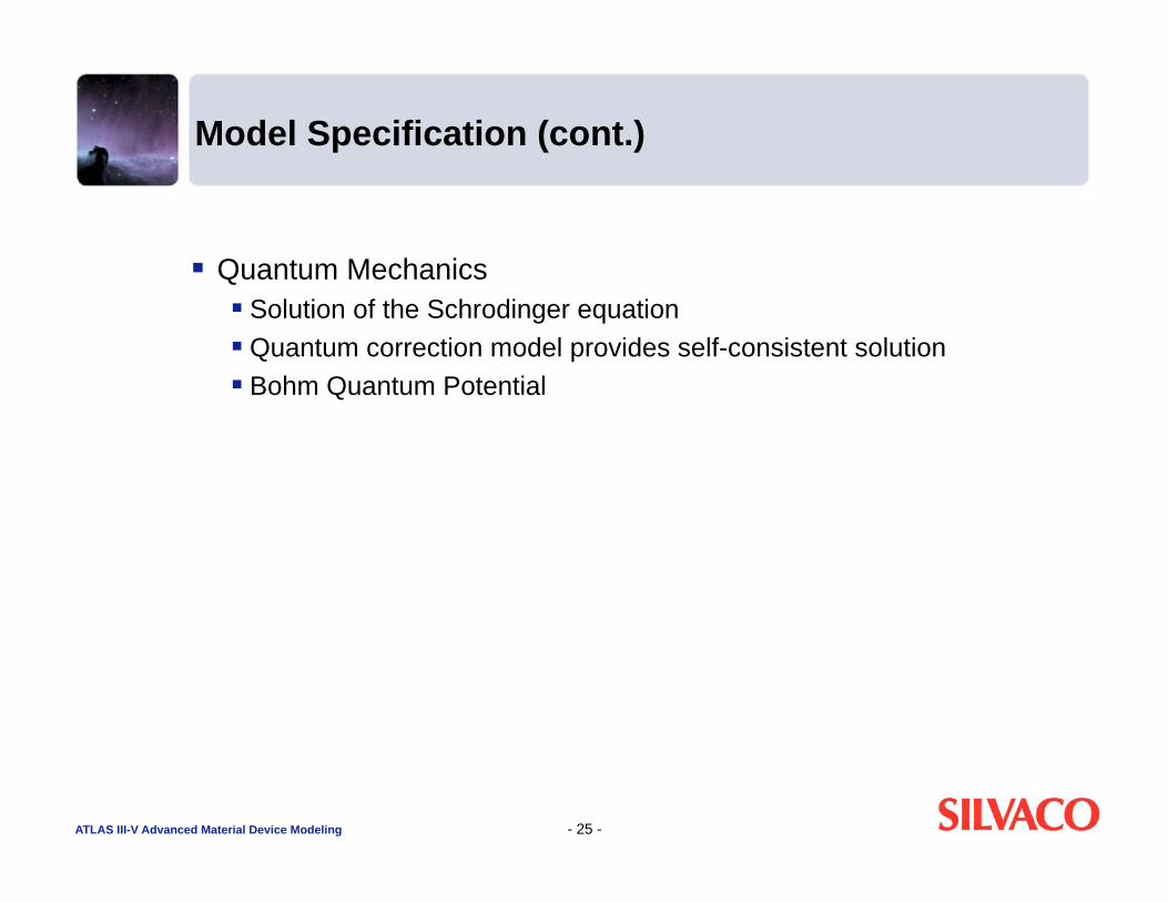
Model Specification (cont.)
Quantum Mechanics
Solution of the Schrodinger equation
Quantum correction model provides self-consistent solution
Bohm Quantum Potential
- 25 -

ATLAS III-V Advanced Material Device Modeling
Solution Techniques
The Mesh
Critical for accurate and robust simulations
Solution Methods
Newton (3 - 6 equations)
Gummel
Block
Number of Carriers
0 / 1 / 2
Solution Type
DC
Transient
AC
Curve Tracer
- 26 -
ATLAS III-V Advanced Material Device Modeling
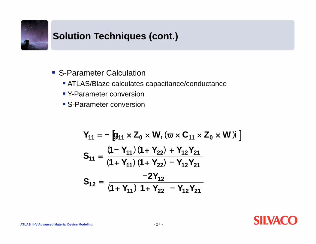
Solution Techniques (cont.)
S-Parameter Calculation
ATLAS/Blaze calculates capacitance/conductance
Y-Parameter conversion
S-Parameter conversion
- 27 -
Y g Z W C Z W i
S Y Y Y Y
Y Y Y Y
S Y
Y Y Y Y
11 11 0 11 0
11 11 22 12 21
11 22 12 21
12 12
11 22 12 21
1 1
1 1
2
1 1
=
=+ +
+ +
=+ +
, ( )
( ) ( )
( ) ( )
( )

ATLAS III-V Advanced Material Device Modeling
Solution Techniques (cont.)
Fast Fourier Transform
Log file data generated by Blaze can be transformed from the time
domain to the frequency domain by using the FFT statement
The frequency domain data can be displayed using TonyPlot
Circuit Simulation
Using the MixedMode module, up to 10 ATLAS devices can be
embedded in a circuit simulation
- 28 -
ATLAS III-V Advanced Material Device Modeling
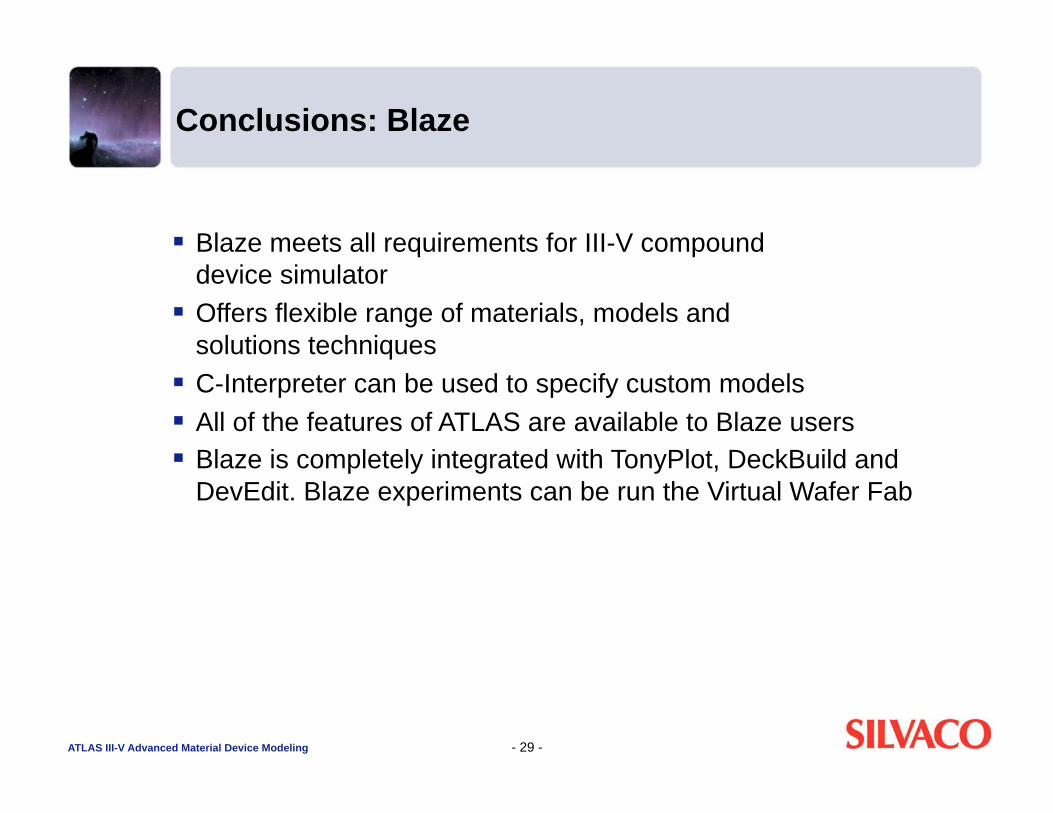
Conclusions: Blaze
Blaze meets all requirements for III-V compound
device simulator
Offers flexible range of materials, models and
solutions techniques
C-Interpreter can be used to specify custom models
All of the features of ATLAS are available to Blaze users
Blaze is completely integrated with TonyPlot, DeckBuild and
DevEdit. Blaze experiments can be run the Virtual Wafer Fab
- 29 -
Simulation of III-V Device with Blaze and SiC
Simulation of III-V Device with Blaze and SiC
ATLAS III-V Advanced Material Device Modeling
SiC as Part of the ATLAS Framework
Simulation of Silicon Carbide devices using anisotropic mobility
models is implemented as part of the ATLAS device simulation
framework
ATLAS provides framework integration
Blaze provides III-V device simulation
SiC provides anisotropic mobility models
- 31 -
ATLAS III-V Advanced Material Device Modeling
Overview of SiC
SiC works within the framework of ATLAS and Blaze. ATLAS
provides the framework integration. Blaze provide electrical
simulation of heterostructure devices and material models for
common III-V semiconductors
Hall mobilities in Silicon Carbide are different depending on the
crystalline axis where conduction takes place
This “anisotropic” mobility could dramatically affect device
simulation results, particularly in power devices where current
flow may be fully two-dimensional
- 32 -
ATLAS III-V Advanced Material Device Modeling
Features of SiC
Automatically accounts for the change in mobility as the current
vector moves through 360 degrees
User just specifies the mobility parameters in the two
crystallographic planes
Works with all of the existing mobility models in ATLAS
and Blaze
- 33 -

ATLAS III-V Advanced Material Device Modeling
Syntax
Anisotropic mobility model syntax
First define mobility in plane <1100>
MOBILITY MATERIAL=b-SiC VSATN=2e7 VSATP=2e7 BETAN=2 \
BETAP=2 MU1N.CAUG=10 MU2N.CAUG=410 \
NCRITN.CAUG=13e17 DELTAN.CAUG=0.6 \
GAMMAN.CAUG=0 ALPHAN.CAUG=-3 BETAN.CAUG=-3 \
MU1P.CAUG=20 MU2P.CAUG=95 NCRITP.CAUG=1E19 \
DELTAP.CAUG=0.5 GAMMAP.CAUG=0 \
ALPHA[.CAUG=-3 BETAP.CAUG=-3
Now define mobility in plane <1000>
MOBILITY MATERIAL=b-SiC N.ANGLE=90.0 VSATN=2E7 \
VSATP=2e7 BETAN=2 BETAP=2 MU1N.CAUG=5 \
MU2N.CAUG=80 NCRITN.CAUG=13e17 \
DELTAN.CAUG=0.6 GAMMAN.CAUG=0
\ ALPHAN.CAUG=-3 BETAN.CAUG=-3
MU1P.CAUG=2.5 \ MU2P.CAUG=20 NCRITP.CAUG=1e19
DELTAP.CAUG=0.5 \ GAMMAP.CAUG=0.0 ALPHAP.CAUG=-3
BETAP.CAUG=-3
- 34 -
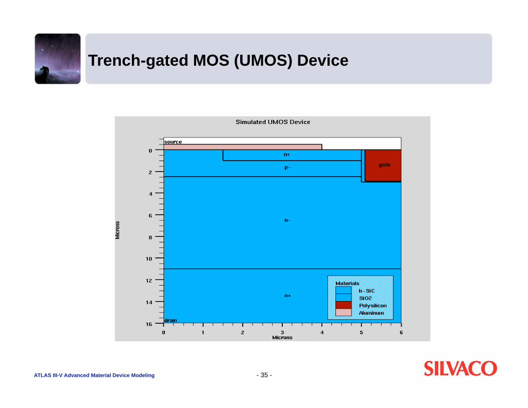
ATLAS III-V Advanced Material Device Modeling
Trench-gated MOS (UMOS) Device
- 35 -

ATLAS III-V Advanced Material Device Modeling
Id-Vd Characteristics for UMOS Device
- 36 -

ATLAS III-V Advanced Material Device Modeling
Double Implanted MOS (DIMOS) Device
- 37 -

ATLAS III-V Advanced Material Device Modeling
Id-Vd Characteristics for DIMOS Device
- 38 -

ATLAS III-V Advanced Material Device Modeling
Conclusions: SiC
Hall mobilities in SiC are different depending on the crystalline
axis
User just needs to specify mobility parameters in the
crystallographic planes
Change in mobility due to current flow vector automatically
calculated
Works with all ATLAS and Blaze mobility models
- 39 -

Simulation of III-V Device with Blaze and Laser
ATLAS III-V Advanced Material Device Modeling
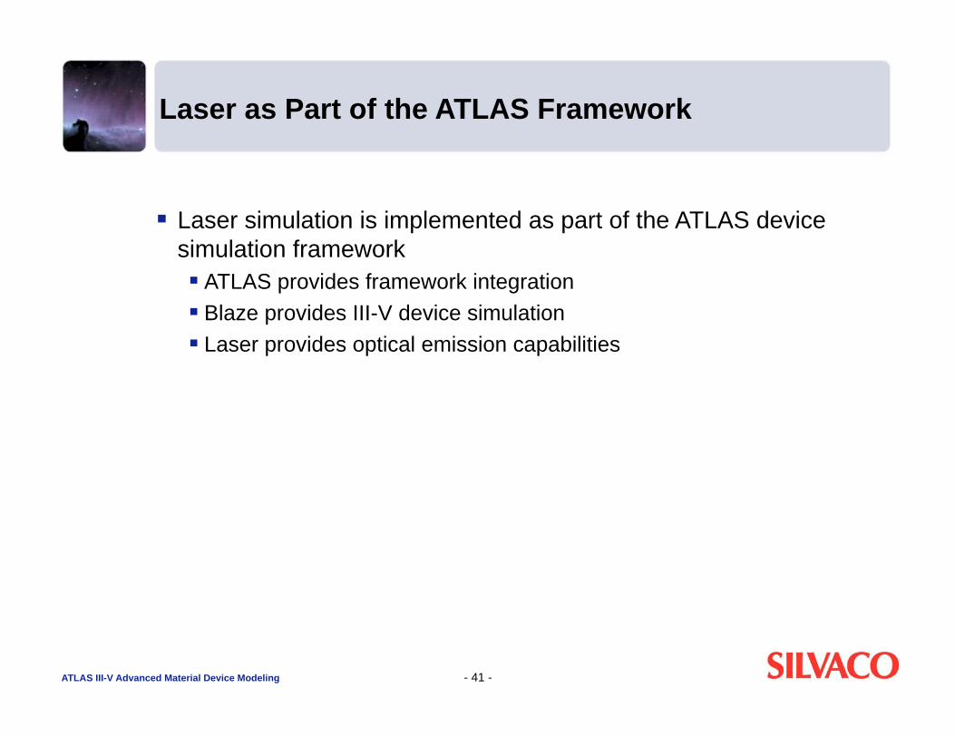
Laser as Part of the ATLAS Framework
Laser simulation is implemented as part of the ATLAS device
simulation framework
ATLAS provides framework integration
Blaze provides III-V device simulation
Laser provides optical emission capabilities
- 41 -

ATLAS III-V Advanced Material Device Modeling
Overview of Laser
Laser works within the framework of ATLAS and Blaze. ATLAS
provides the framework integration. Blaze provide electrical
simulation of heterostructure devices and material models for
common III-V semiconductors
Self-consistently solves the Helmholtz equation to calculate
optical field and photon densities
Accounts for carrier recombination due to stimulated emission
Calculates optical gain which depends on photon energy and quasi-Fermi levels
Predicts laser light output power and light intensity profiles
corresponding to the fundamental transverse mode
Calculates the light output and modal gain spectra for multiple
longitudinal modes
For Quantum wells optical gain accounts for bound state energies
- 42 -

ATLAS III-V Advanced Material Device Modeling
Features of Laser
Arbitrary stripe geometries
Devices with multiple insulators and electrodes
Allows any material as the active layer
Delta doped layers
Standard Blaze III-V, II-VI and GaN materials supported
DC and transient modes of operation
Near field and far field patterns, spectra and I-V curves
- 43 -
ATLAS III-V Advanced Material Device Modeling
Laser Solution Methodology
Blaze is used to obtain the initial dc starting condition by solving
Poisson’s equation
Electron continuity equation
Hole continuity equation
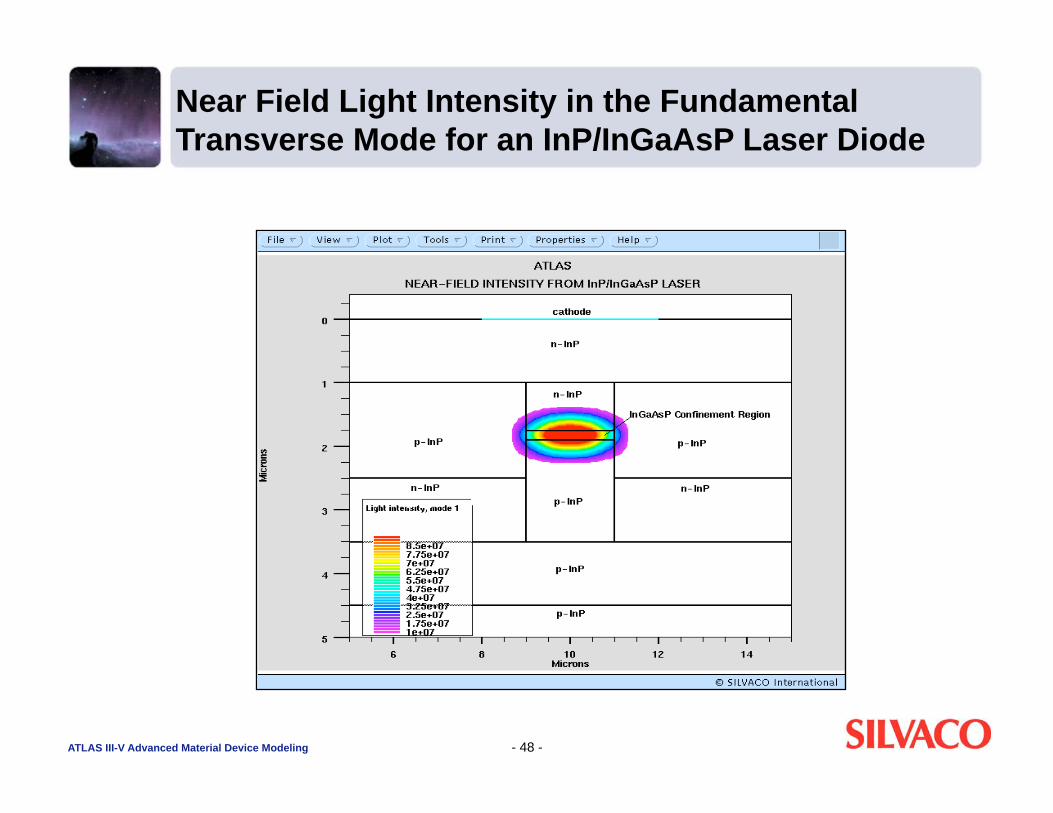
Laser solves the 2D Helmholtz equation to find the transverse
optical field profile E(x,y)
E(x,y) is found for the fundamental transverse mode
The Helmholtz equation may be solved for either
a single longitudinal mode of greatest optical power
multiple longitudinal modes
Multiple transverse modes can also be simulated
- 44 -
ATLAS III-V Advanced Material Device Modeling
Laser Solution Methodology (cont.)
The central model in laser simulation is the optical gain model
which is the ability of the semiconductor media to amplify light.
Laser contains three gain models
Empirically based model. This has no frequency dependence and is
only a function of carrier concentrations
Physically based model. This takes into account frequency dependence and may be used for spectral analysis when simulating
multiple longitudinal modes
Quantum well model. This accounts for optical gain within quantum
wells including effects of bound state energies
- 45 -

ATLAS III-V Advanced Material Device Modeling
Laser Solution Methodology (cont.)
Laser uses E(x,y) and g(x,y) to solve the photon rate equation, to
calculate the total photon density for each longitudinal mode
Blaze and Laser simulations are coupled in three areas
the optical gain g(x,y) is a function of the quasi-Fermi levels
the dielectric permittivity is a function of the optical
gain g(x,y)
an additional optical recombination term is added to the RHS of the
continuity equations and is a function of g(x,y), E(x,y) and the photon
density
- 46 -
ATLAS III-V Advanced Material Device Modeling
Output from Laser
Single mode operation
optical intensity profile E(x,y)
laser gain g(x,y)
photon density
optical power
total optical gain
Multiple mode operation
all single mode output but summed over all modes
laser spectra file for each dc bias or transient solutions
- 47 -
ATLAS III-V Advanced Material Device Modeling
Near Field Light Intensity in the Fundamental
Transverse Mode for an InP/InGaAsP Laser Diode
- 48 -

ATLAS III-V Advanced Material Device Modeling
Optical Gain as a Function of Bias
- 49 -
ATLAS III-V Advanced Material Device Modeling
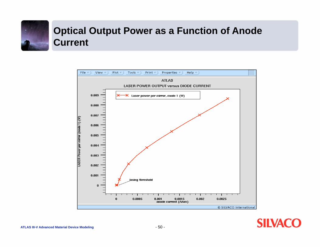
Optical Output Power as a Function of Anode
Current
- 50 -
ATLAS III-V Advanced Material Device Modeling
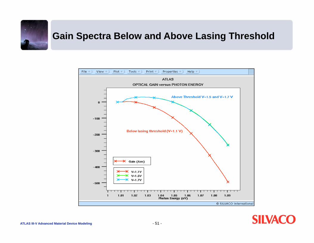
Gain Spectra Below and Above Lasing Threshold
- 51 -

ATLAS III-V Advanced Material Device Modeling
Laser Spectrum Above Threshold
- 52 -

ATLAS III-V Advanced Material Device Modeling
Near Field Pattern for a Strip Laser
- 53 -

ATLAS III-V Advanced Material Device Modeling
Threshold and Sub-Threshold Characteristics
for a Strip Laser
- 54 -

ATLAS III-V Advanced Material Device Modeling
Fundamental Transverse Mode Near
Field Light Intensity
- 55 -
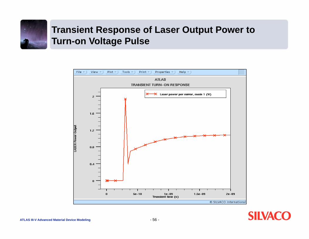
ATLAS III-V Advanced Material Device Modeling
Transient Response of Laser Output Power to
Turn-on Voltage Pulse
- 56 -
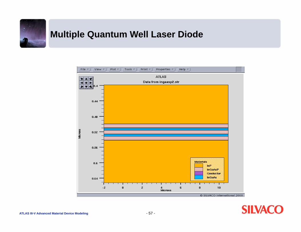
ATLAS III-V Advanced Material Device Modeling
Multiple Quantum Well Laser Diode
- 57 -
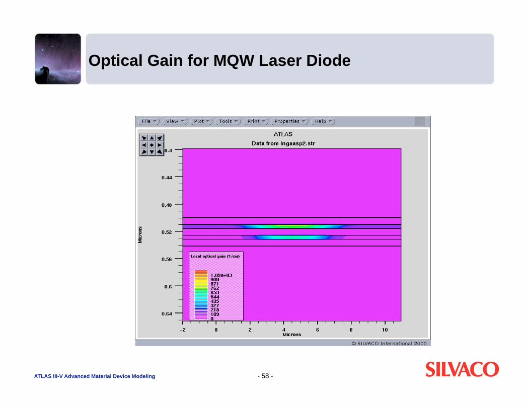
ATLAS III-V Advanced Material Device Modeling
Optical Gain for MQW Laser Diode
- 58 -

ATLAS III-V Advanced Material Device Modeling
Conclusions: Laser
By solving the Helmholtz equation with optical gain models
Laser allows accurate simulation of laser diode
Multiple quantum well and strained MQW laser diodes
Analysis of the effects of structures design and material
parameters is straightforward
Near field and far field patterns allow improved laser diode designs to be made
Seamless integration into Blaze allows users to quickly implement
laser device simulations and study results with TonyPlot
- 59 -