ata5771c/73c/74c - microchip technology
TRANSCRIPT

ATA5771C/73C/74C
UHF ASK/FSK Transmitter with the Atmel AVRMicrocontroller
DATASHEET
General Features
● Atmel® AVR® microcontroller and RF transmitter PLL in a single QFN24
5mm × 5mm package (pitch 0.65mm)
● Operating frequency ranges 310MHz to 350MHz, 429MHz to 439MHz and 868MHz to 928MHz
● Temperature range –40°C to +85°C
● Supply voltage 2.0V to 3.6V allowing usage of single Li-cell power supply
● Low power consumption
● Active mode: typical 9.8mA at 3.0V and 4MHz microcontroller-clock● Power-down mode: Typical 200nA at 3.0V
● Modulation scheme ASK/FSK
● Integrated PLL loop filter
● Output power of 8dBm at 315MHz / 7.5dBm at 433.92MHz / 5.5dBm at 868.3MHz
● Easy to design-in due to excellent isolation of the PLL from the PA and power
supply
● Single-ended antenna output with high efficient power amplifier
● Very robust ESD protection: HBM 2500V, MM100V, CDM 1000V
● High performance, low power AVR 8-bit microcontroller
● Advanced RISC architecture
● Non-volatile program and data memories
● 4Kbytes of in-system programmable program memory flash● 256Bytes in-system programmable EEPROM● 256Bytes internal SRAM
● Programming lock for self-programming flash program and EEPROM data security
● Peripheral features
● Two timer/counter, 8- and 16-bit counters with two PWM channels on both● 10-bit ADC● On-chip analog comparator● Programmable watchdog timer with separate on-chip oscillator● Universal serial interface (USI)
9137J-RKE-10/14

● Special microcontroller features
● debugWIRE on-chip debug system● In-system programmable via SPI port● External and internal interrupt sources● Pin change interrupt on 12 pins● Enhanced power-on reset circuit● Programmable brown-out detection circuit● Internal calibrated oscillator● On-chip temperature sensor
● 12 programmable I/O lines
ATA5771C/73C/74C [DATASHEET]9137J–RKE–10/14
2

1. General Description
The Atmel® ATA5771C/73C/74C is a highly flexible programmable transmitter containing the Atmel AVR® microcontroller Atmel ATtiny44V and the UHF PLL transmitters in a small QFN24 5mm × 5mm package. This device is a member of a transmitter family covering several operating frequency ranges, which has been specifically developed for the demands of RF low-cost data transmission systems with data rates up to 32kBit/s using ASK or FSK modulation. Its primary applications are in the application of Remote Keyless-Entry (RKE), Passive Entry Go (PEG) System and Remote Start. The ATA5771 is designed for 868MHz application, whereas ATA5773 for 315MHZ application and ATA5774 for 434MHz application.
Figure 1-1. ASK System Block Diagram
UHF ASK/FSKRemote Control Receiver
UHF ASK/FSKRemote Control Transmitter
Atmel ATA577x
Antenna
LoopAntenna
VS
VS
1 to 6 Micro-controllerDemod
VCC_RF
GND_RF
PA_ENABLE
ENABLE
Control
XTOPLL
VCOLNA
XTO
PA
VCO
f/4 PLL
Powerup/down
ANT1
ANT2
PXYS1
S1
S1
PXY
PXY
PXY
PXY
PXY
PXY
VDD
GND
PXY
PXY
PXY
PXY
PXY
VS
CLK
3ATA5771C/73C/74C [DATASHEET]9137J–RKE–10/14

Figure 1-2. FSK System Block Diagram
UHF ASK/FSKRemote Control Receiver
UHF ASK/FSKRemote Control Transmitter
Atmel ATA577x
Antenna
LoopAntenna
VS
VS
1 to 6 Micro-controllerDemod
VCC_RF
GND_RF
PA_ENABLE
ENABLE
Control
XTOPLL
VCOLNA
XTO
PA
VCO
f/4 PLL
Powerup/down
ANT1
ANT2
PXYS1
S1
S1
PXY
PXY
PXY
PXY
PXY
PXY
VDD
GND
PXY
PXY
PXY
PXY
PXY
CLK
VS
ATA5771C/73C/74C [DATASHEET]9137J–RKE–10/14
4

2. Pin Configuration
Figure 2-1. Pinning QFN24 5mm × 5mm
Table 2-1. Pin Description
Pin Symbol Function
1 VCC Microcontroller supply voltage
2 PB0 Port B is a 4-bit bi-directional I/O port with internal pull-up resistor
3 PB1 Port B is a 4-bit bi-directional I/O port with internal pull-up resistor
4 PB3/RESET Port B is a 4-bit bi-directional I/O port with internal pull-up resistor/reset input
5 PB2 Port B is a 4-bit bi-directional I/O port with internal pull-up resistor
6 PA7 Port A is an 8-bit bi-directional I/O port with internal pull-up resistor
7 PA6 / MOSI Port A is an 8-bit bi-directional I/O port with internal pull-up resistor
8 CLKClock output signal for microcontroller. The clock output frequency is set by the crystal to fXTAL/4
9 PA_ENABLE Switches on power amplifier. Used for ASK modulation
10 ANT2 Emitter of antenna output stage
11 ANT1 Open collector antenna output
12 GND Ground
13 PA5/MISO Port A is an 8-bit bi-directional I/O port with internal pull-up resistor
14 PA4/SCK Port A is an 8-bit bi-directional I/O port with internal pull-up resistor
15 PA3/T0 Port A is an 8-bit bi-directional I/O port with internal pull-up resistor
16 PA2 Port A is an 8-bit bi-directional I/O port with internal pull-up resistor
17 PA1 Port A is an 8-bit bi-directional I/O port with internal pull-up resistor
18 PA0 Port A is an 8-bit bi-directional I/O port with internal pull-up resistor
19 GND Microcontroller ground
20 XTAL Connection for crystal
21 VS_RF Transmitter supply voltage
22 GND_RF Transmitter ground
23 ENABLE Enable input
24 GND Ground
GND Ground/backplane (exposed die pad)
PB3/RESET
PB2
PA7
PB1
PB0
VCC
PA3/T0
PA4/USCK
PA5/MISO
PA2
PA1
PA0
VS
_RF
XTA
L
GN
D
GN
D_R
F
EN
AB
LE
GN
D
AN
T2
AN
T1
GN
D
PA_E
NA
BLE
CLK
PA6/
MO
SI
24
4
3
6
5
2
1
15
16
13
14
17
1823 22 21 20 19
7 8 9 10 11 12
5ATA5771C/73C/74C [DATASHEET]9137J–RKE–10/14

2.1 Pin Configuration of RF Pins
Table 2-2. Pin Description
Pin Symbol Function Configuration
8 CLK
Clock output signal for microcontroller.
The clock output frequency is set by the crystal to fXTAL/4.
9 PA_ENABLESwitches on power amplifier.
Used for ASK modulation.
10
11
ANT2
ANT1
Emitter of antenna output stage.
Open collector antenna output.
20 XTAL Connection for crystal.
100Ω
100ΩCLK
VS
50kΩ
20μA
UREF = 1.1VPA_ENABLE
ANT1
ANT2
1.5kΩ 1.2kΩ
182μA
XTAL
VS VS
ATA5771C/73C/74C [DATASHEET]9137J–RKE–10/14
6

21 VS Supply voltageSee ESD protection circuitry (see Figure 5-1 on page 155).
22 GND GroundSee ESD protection circuitry (see Figure 5-1 on page 155).
23 ENABLE Enable input
Table 2-2. Pin Description (Continued)
Pin Symbol Function Configuration
200kΩENABLE
7ATA5771C/73C/74C [DATASHEET]9137J–RKE–10/14

3. Functional Description
Figure 1-1 on page 3 and Figure 1-2 on page 4 show the interconnections between the microcontroller and the RF part for a typical application. In the recommended application circuits the clock output of the RF transmitter is connected to the microcontroller in order to be able to generate data rate with tolerance lower than 3%. The transmitter’s crystal oscillator (XTO), phase locked loop (PLL) and clock generation are started using pin ENABLE. The power amplifier (PA) is activated using the connection to the pin PA_ENABLE. The FSK modulation is performed due to pulling of the crystal load capacitance for this purpose the microcontroller out put port together with an external switch applies this modulation technique. For the ASK modulation the power amplifier will be switched on and of by modulating the PA_ENABLE pin due to the data.
To wake up the system from standby mode at least one event is required, which will be performed by pushing tone button. After this event the microcontroller starts up with the internal RC oscillator. For the TX operation the user software must additionally control just 2 pins, the pin ENABLE and pin PA_ENABLE. In case of the FSK modulation one additional connection from microcontroller is necessary to perform the pulling of the crystal load capacitance.
If ENABLE and PA_ENABLE are set to LOW the transmitter is in standby mode with the suitable mode setting of the microcontroller (MCU) the power consumption will be reduced.
If ENABLE is set to HIGH and PA_ENABLE to LOW, the XTO, PLL, and the Clock driver of the RF transmitter are activated and the VCO frequency is 32 times the XTO frequency. The Atmel ATA5771 and Atmel ATA5774 require typically shorter than 1 ms until the PLL is locked and the transmitter’s clock output is stable, while the Atmel ATA5773 requires time shorter than 3 ms for this progress.
If both ENABLE and PA_ENABLE are set to HIGH the whole RF transmitter (XTO, PLL, Clock driver and power Amplifier) is activated. The ASK modulation is achieved by switching on and off the power amplifier via pin PA_ENABLE. The FSK modulation is performed by pulling the crystal load capacitor which will change the reference frequency of the PLL due to the data. The microcontroller modulates the load capacitance of the crystal using an external switch. A MOS transistor with a low parasitic capacitance is recommended to be used for this purpose. During the FSK modulation is the PA_ENABLE pin set to HIGH.
To generate the data for the telegram the internal RC oscillator of the microcontroller is not accurate enough because this will be affected by ambient temperature and operating voltage. To reduce the variation of the data rate lower than 3% the clock frequency generated by the RF transmitter should be used as a reference. The MCU has to wait at least longer than 3ms for ATA5773 after setting ENABLE to HIGH, before the clock output from the RF transmitter can be used. For ATA5771 and ATA5774 the MCU must wait longer than 1 ms until the clock output is stable. The clock output with the crystal tolerance is connected to the timer0 of the MCU. This timer clocks the USI to generate the data rate. In the Two serial synchronous data transfer modes will be provided by USI. This will be pass out with different physical I/O ports, two wire mode is used for ASK and the three wire mode for FSK.
3.1 Frequency Generation
In Atmel ATA5773 and Atmel ATA5774 the VCO is locked to 32 times crystal frequency hence the following crystal is needed
● 9.8438MHz for 315MHz application
● 13.56MHz for 433.92MHz application
The VCO of ATA5771 is locked to 64 times crystal frequency therefore the necessary crystal frequency is
● 13.5672MHz for 868.3MHz application
● 14.2969MHz for 915MHz application
Due to the high integration the PLL and VCO peripheral elements are integrated.
The XTO is a series resonance oscillator that only one capacitor together with a crystal connected in series to GND are needed as external elements. Until the PLL and clock output is stable the following time can be expected
● 3ms for ATA5773
● 1ms for ATA5771 and ATA5774
Therefore, a time delay of ≥ 3 ms for ATA5773 and ≥ 1ms for ATA5771/74 between activation of pin ENABLE and switching on the pin PA_ENABLE must be implemented in the software.
ATA5771C/73C/74C [DATASHEET]9137J–RKE–10/14
8

3.2 ASK Transmission
The ASK modulation will performed by switching the power amplifier on and of due to the data to be transmitted. The transmitter’s XTO and PLL are activated by setting the pin ENABLE to HIGH. Between the activation of the pin ENABLE and the pin PA_ENABLE minimum 3ms time delay must be taken into account for the application with ATA5773, whereas a minimum 1ms time delay for an application using ATA5771 or ATA5774. After the mentioned time delay the generated clock frequency by the RF transmitter can be used as reference for the data generation of the microcontroller block.
3.3 FSK Transmission
The transmitter’s XTO and PLL are activated by setting the pin ENABLE to HIGH. Like the ASK transmission a defined time delay must be taken into account between the activation of the pin ENABLE and the pin PA_ENABLE. After this time delay the clock frequency can be used as reference for the data rate generation and the data transmission using FSK modulation is ready. For this purpose an additional capacitor to the crystal’s load capacitor will be switched between the high impedance and ground due to the data rate. Thus the reference frequency, which is crystal frequency, of the RF transmitter will be modulated. This results also in the transmitted spectrum. It is important that the switching element must have a defined low parasitic capacitance.
The accuracy of the frequency deviation with XTAL pulling method is about ±25% when the following tolerances are considered.
Figure 3-1. Tolerances of Frequency Modulation
Using C4 = 8.2pF ±5%, C5 = 10pF ±5%, a switch port with CSwitch = 3pF ±10%, stray capacitances on each side of the crystal of CStray1 = CStray2 = 1pF ±10%, a parallel capacitance of the crystal of C0 = 3.2pF ±10% and a crystal with CM = 13fF ±10%, results in a typical FSK deviation of ±21.5kHz with worst case tolerances of ±16.25kHz to ±28.01kHz.
3.4 CLK Output
RF transmitter generated clock signal based on the devided crystal frequency. This will be available for the microcontroller as reference. The delivered signal is CMOS compatible if the load capacitance is lower than 10pF.
3.4.1 Clock Pulse Take-over
The clock of the crystal oscillator can be used for clocking the microcontroller, which starts with an integrated RC-oscillator. After the generated clock signal of the RF transmitter is stable, the microcontroller will take over the clock signal and use it as reference generating the data rate, so that the message can be transmitted with crystal accuracy.
RS
LM C4
CM
VS
XTAL
Crystal equivalent circuit
C0 C5
CSwitch
CStray1 CStray2
9ATA5771C/73C/74C [DATASHEET]9137J–RKE–10/14

3.4.2 Output Matching and Power Setting
The power amplifier is an open-collector output delivering a current pulse, which is nearly independent from the load impedance. Thus the delivered output power can be tuned via the load impedance of the antenna and the matching elements. This output configuration enables simple matching to any kind of antenna or to 50Ω which results in a high power efficiency {η = Pout/(IS,PA VS) }. The maximum output power can be achieved at 3V supply voltage when the load impedance is optimized to
● ZLoad = (255 + j192)Ω for the Atmel ATA5773 with the power efficiency of 40%
● Background: The current pulse of the power amplifier is 9mA and the maximum output power is delivered to a resistive load of 400Ω if the 1.0pF output capacitance of the power amplifier is compensated by the load impedance. And thus the load impedance of ZLoad = 400Ω || j/(2 × π × f × 1.0pF) = (255 + j192)Ω is achieved for the maximum output power of 8dBm.
● ZLoad = (166 + j223)Ω for the Atmel ATA5774 with the power efficiency of 36%
● Background: The current pulse of the power amplifier is 9mA and the maximum output power is delivered to a resistive load of 465Ω if the 1.0pF output capacitance of the power amplifier is compensated by the load impedance. And thus the load impedance of ZLoad = 465Ω || j/(2 × π × f × 1.0pF) = (166 + j223)Ω is achieved for the maximum output power of 7.5dBm.
● ZLoad = (166 + j226)Ω for the Atmel ATA5771 with the power efficiency of 24%
● Background: The current pulse of the power amplifier is 7.7mA and the maximum output power is delivered to a resistive load of 475Ω if the 0.53pF output capacitance of the power amplifier is compensated by the load impedance. And thus the load impedance of ZLoad = 475Ω || j/(2 × π × f × 0.53pF) = (166 + j226)Ω is achieved for the maximum output power of 5.5dBm.
The load impedance is defined as the impedance seen from the power amplifier (pin ANT1 and pin ANT2) into the matching network. This large signal load impedance should not be mixed up with the small signal input impedance delivered as input characteristic of RF amplifiers and measured from the application into the IC, instead of from the IC into the application. Please take note that there must be a low resistive path between the VS and the collector output of the PA to deliver the DC current. Reduced output power will be achieved by lowering the real parallel part of the load impedance where the parallel imaginary part should be kept constant.
Output power measurement can be performed using the circuit shown in Figure 3-2. Note that the component values must be changed to compensate for the individual board parasitics until the RF power amplifier has the right load impedance. In addition, the damping of the cable used to measure the output power must be calibrated out.
Figure 3-2. Output Power Measurement Atmel ATA5771C/73C/74C
L1 = 47nH
C2 = 3.3pF
C1 = 1nF
VS
Rin
ANT2
ANT1
ZLopt
Powermeter
50Ω
Z = 50Ω
ATA5771C/73C/74C [DATASHEET]9137J–RKE–10/14
10

4. Microcontroller Block
These data are referred to the data base of microcontroller Atmel ATtiny44V.
4.1 Overview
The ATtiny44V is a low-power CMOS 8-bit microcontroller based on the Atmel AVR® enhanced RISC architecture. By executing powerful instructions in a single clock cycle, the ATtiny44V achieves throughputs approaching 1MIPS per MHz allowing the system designer to optimize power consumption versus processing speed.
4.2 Block Diagram
Figure 4-1. Block Diagram
ProgramCounter
ProgramFlash
StackPointer
WatchdogTimer
InternalOscillator
InternalCalibratedOscillator
Timingand Control
MCU ControlRegister
MCU StatusRegister
Timer/Counter0
Timer/Counter1
InterruptUnit
SRAM
8-bit Databus
GND
VCC
EEPROM Oscillators
ALU
XYZ
GeneralPurposeRegisters
InstructionRegister
StatusRegister
InstructionDecoder
ProgrammingLogic
Data RegisterPort A
Ana
log
Com
para
tor
Port A Drivers
Data DirectionRegister Port A
ADC Data RegisterPort B
Data RegisterPort B
Port B Drivers
PA7 to PA0 PB3 to PB0
ISPInterface
+ -
ControlLines
11ATA5771C/73C/74C [DATASHEET]9137J–RKE–10/14

The Atmel AVR® core combines a rich instruction set with 32 general purpose working registers. All the 32 registers are directly connected to the Arithmetic Logic Unit (ALU), allowing two independent registers to be accessed in one single instruction executed in one clock cycle. The resulting architecture is more code efficient while achieving throughputs up to ten times faster than conventional CISC microcontrollers.
The Atmel ATtiny44V provides the following features: 4K byte of In-System Programmable Flash, 256 bytes EEPROM, 256 bytes SRAM, 12 general purpose I/O lines, 32 general purpose working registers, a 8-bit Timer/Counter with two PWM channels, a 16-bit timer/counter with two PWM channels, Internal and External Interrupts, a 8-channel 10-bit ADC, programmable gain stage (1x, 20x) for 12 differential ADC channel pairs, a programmable watchdog timer with internal oscillator, internal calibrated oscillator, and three software selectable power saving modes. The Idle mode stops the CPU while allowing the SRAM, Timer/Counter, ADC, analog comparator, and interrupt system to continue functioning. The power-down mode saves the register contents, disabling all chip functions until the next interrupt or hardware reset. The ADC noise reduction mode stops the CPU and all I/O modules except ADC, to minimize switching noise during ADC conversions. In standby mode, the crystal/resonator oscillator is running while the rest of the device is sleeping. This allows very fast start-up combined with low power consumption.
The device is manufactured using the Atmel high density non-volatile memory technology. The On-chip ISP Flash allows the program memory to be re-programmed in-system through an SPI serial interface, by a conventional non-volatile memory programmer or by an on-chip boot code running on the AVR core.
The ATtiny44V AVR is supported with a full suite of program and system development tools including: C compilers, macro assemblers, program debugger/simulators, in-circuit emulators, and evaluation kits.
4.3 Automotive Quality Grade
The ATtiny44V have been developed and manufactured according to the most stringent requirements of the international standard ISO-TS-16949 grade 1. This datasheet contains limit values extracted from the results of extensive characterization (temperature and voltage). The quality and reliability of the ATtiny44V have been verified during regular product qualification as per AEC-Q100.
As indicated in the ordering information paragraph, the product is available in only one temperature grade.
Table 4-1. Temperature Grade Identification for Automotive Products
Temperature
Temperature
Identifier Comments
–40°C; +125°C Z Full automotive temperature range
ATA5771C/73C/74C [DATASHEET]9137J–RKE–10/14
12

4.4 Pin Descriptions
4.4.1 VCC
Supply voltage.
4.4.2 GND
Ground.
4.4.3 Port B (PB3...PB0)
Port B is a 4-bit bi-directional I/O port with internal pull-up resistors (selected for each bit). The port B output buffers have symmetrical drive characteristics with both high sink and source capability except PB3 which has the RESET capability. To use pin PB3 as an I/O pin, instead of RESET pin, program (‘0’) RSTDISBL fuse. As inputs, Port B pins that are externally pulled low will source current if the pull-up resistors are activated. The port B pins are tri-stated when a reset condition becomes active, even if the clock is not running.
Port B also serves the functions of various special features of the Atmel ATtiny44V as listed on Section 4.14.3 “Alternate Port Functions” on page 57.
4.4.4 RESET
Reset input. A low level on this pin for longer than the minimum pulse length will generate a reset, even if the clock is not running. The minimum pulse length is given in Figure 4-13 on page 39. Shorter pulses are not guaranteed to generate a reset.
4.4.5 Port A (PA7...PA0)
Port A is a 8-bit bi-directional I/O port with internal pull-up resistors (selected for each bit). The port A output buffers have symmetrical drive characteristics with both high sink and source capability. As inputs, port A pins that are externally pulled low will source current if the pull-up resistors are activated. The Port A pins are tri-stated when a reset condition becomes active, even if the clock is not running.
Port A has an alternate functions as analog inputs for the ADC, analog comparator, timer/counter, SPI and pin change interrupt as described in Section 4.14.3 “Alternate Port Functions” on page 57.
4.5 Resources
A comprehensive set of development tools, drivers and application notes, and datasheets are available for download on http://www.atmel.com/avr.
4.6 About Code Examples
This documentation contains simple code examples that briefly show how to use various parts of the device. These code examples assume that the part specific header file is included before compilation. Be aware that not all C compiler vendors include bit definitions in the header files and interrupt handling in C is compiler dependent. Please confirm with the C compiler documentation for more details.
For I/O registers located in extended I/O map, “IN”, “OUT”, “SBIS”, “SBIC”, “CBI”, and “SBI” instructions must be replaced with instructions that allow access to extended I/O. Typically “LDS” and “STS” combined with “SBRS”, “SBRC”, “SBR”, and “CBR”.
13ATA5771C/73C/74C [DATASHEET]9137J–RKE–10/14

4.7 CPU Core
4.7.1 Overview
This section discusses the Atmel AVR® core architecture in general. The main function of the CPU core is to ensure correct program execution. The CPU must therefore be able to access memories, perform calculations, control peripherals, and handle interrupts.
4.7.2 Architectural Overview
Figure 4-2. Block Diagram of the Atmel AVR Architecture
In order to maximize performance and parallelism, the AVR uses a Harvard architecture – with separate memories and buses for program and data. Instructions in the program memory are executed with a single level pipelining. While one instruction is being executed, the next instruction is pre-fetched from the Program memory. This concept enables instructions to be executed in every clock cycle. The program memory is in-system reprogrammable flash memory.
The fast-access register File contains 32 x 8-bit general purpose working registers with a single clock cycle access time. This allows single-cycle arithmetic logic unit (ALU) operation. In a typical ALU operation, two operands are output from the register file, the operation is executed, and the result is stored back in the register file – in one clock cycle.
Status andControl
InterruptUnit
32 x 8GeneralPurposeRegisters
ALU
Data Bus 8-bit
DataSRAM
WatchdogTimer
InstructionRegister
InstructionDecoder
AnalogComparator
EEPROM
I/O Lines
UniversalSerial Interface
Control Lines
Dire
ct A
ddre
ssin
g
Indi
rect
Add
ress
ing
Timer/Counter1
Timer/Counter0
ProgramCounter
FlashProgramMemory
ATA5771C/73C/74C [DATASHEET]9137J–RKE–10/14
14

Six of the 32 registers can be used as three 16-bit indirect address register pointers for data space addressing – enabling efficient address calculations. One of the these address pointers can also be used as an address pointer for look up tables in flash program memory. These added function registers are the 16-bit X-, Y-, and Z-register, described later in this section.
The ALU supports arithmetic and logic operations between registers or between a constant and a register. Single register operations can also be executed in the ALU. After an arithmetic operation, the status register is updated to reflect information about the result of the operation.
Program flow is provided by conditional and unconditional jump and call instructions, able to directly address the whole address space. Most Atmel AVR® instructions have a single 16-bit word format. Every program memory address contains a 16- or 32-bit instruction.
During interrupts and subroutine calls, the return address program counter (PC) is stored on the stack. The stack is effectively allocated in the general data SRAM, and consequently the Stack size is only limited by the total SRAM size and the usage of the SRAM. All user programs must initialize the SP in the reset routine (before subroutines or interrupts are executed). The stack pointer (SP) is read/write accessible in the I/O space. The data SRAM can easily be accessed through the five different addressing modes supported in the AVR architecture. The memory spaces in the AVR architecture are all linear and regular memory maps.
A flexible interrupt module has its control registers in the I/O space with an additional global interrupt enable bit in the status register. All interrupts have a separate interrupt vector in the interrupt vector table. The interrupts have priority in accordance with their interrupt vector position. The lower the interrupt vector address, the higher the priority.
The I/O memory space contains 64 addresses for CPU peripheral functions as control registers, SPI, and other I/O functions. The I/O memory can be accessed directly, or as the data space locations following those of the register File, 0x20 - 0x5F.
4.7.3 ALU – Arithmetic Logic Unit
The high-performance AVR ALU operates in direct connection with all the 32 general purpose working registers. Within a single clock cycle, arithmetic operations between general purpose registers or between a register and an immediate are executed. The ALU operations are divided into three main categories – arithmetic, logical, and bit-functions. Some implementations of the architecture also provide a powerful multiplier supporting both signed/unsigned multiplication and fractional format. See the “Instruction Set” section for a detailed description.
4.7.4 Status Register
The status register contains information about the result of the most recently executed arithmetic instruction. This information can be used for altering program flow in order to perform conditional operations. Note that the status register is updated after all ALU operations, as specified in the instruction set reference. This will in many cases remove the need for using the dedicated compare instructions, resulting in faster and more compact code. The status register is not automatically stored when entering an interrupt routine and restored when returning from an interrupt. This must be handled by software.
15ATA5771C/73C/74C [DATASHEET]9137J–RKE–10/14
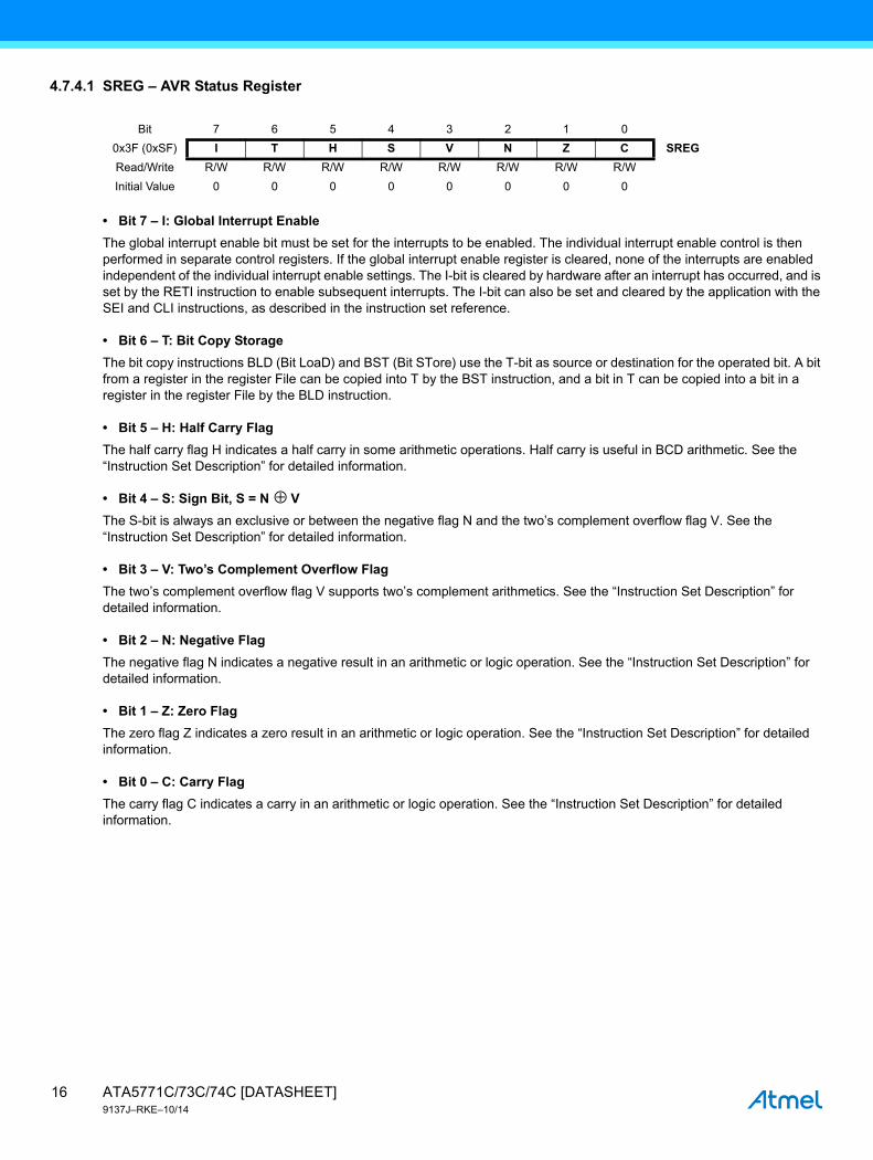
4.7.4.1 SREG – AVR Status Register
• Bit 7 – I: Global Interrupt Enable
The global interrupt enable bit must be set for the interrupts to be enabled. The individual interrupt enable control is then performed in separate control registers. If the global interrupt enable register is cleared, none of the interrupts are enabled independent of the individual interrupt enable settings. The I-bit is cleared by hardware after an interrupt has occurred, and is set by the RETI instruction to enable subsequent interrupts. The I-bit can also be set and cleared by the application with the SEI and CLI instructions, as described in the instruction set reference.
• Bit 6 – T: Bit Copy Storage
The bit copy instructions BLD (Bit LoaD) and BST (Bit STore) use the T-bit as source or destination for the operated bit. A bit from a register in the register File can be copied into T by the BST instruction, and a bit in T can be copied into a bit in a register in the register File by the BLD instruction.
• Bit 5 – H: Half Carry Flag
The half carry flag H indicates a half carry in some arithmetic operations. Half carry is useful in BCD arithmetic. See the “Instruction Set Description” for detailed information.
• Bit 4 – S: Sign Bit, S = N ⊕ V
The S-bit is always an exclusive or between the negative flag N and the two’s complement overflow flag V. See the “Instruction Set Description” for detailed information.
• Bit 3 – V: Two’s Complement Overflow Flag
The two’s complement overflow flag V supports two’s complement arithmetics. See the “Instruction Set Description” for detailed information.
• Bit 2 – N: Negative Flag
The negative flag N indicates a negative result in an arithmetic or logic operation. See the “Instruction Set Description” for detailed information.
• Bit 1 – Z: Zero Flag
The zero flag Z indicates a zero result in an arithmetic or logic operation. See the “Instruction Set Description” for detailed information.
• Bit 0 – C: Carry Flag
The carry flag C indicates a carry in an arithmetic or logic operation. See the “Instruction Set Description” for detailed information.
Bit 7 6 5 4 3 2 1 0
0x3F (0xSF) I T H S V N Z C SREG
Read/Write R/W R/W R/W R/W R/W R/W R/W R/W
Initial Value 0 0 0 0 0 0 0 0
ATA5771C/73C/74C [DATASHEET]9137J–RKE–10/14
16

4.7.5 General Purpose Register File
The register file is optimized for the Atmel® AVR® enhanced RISC instruction set. In order to achieve the required performance and flexibility, the following input/output schemes are supported by the register file:
● One 8-bit output operand and one 8-bit result input
● Two 8-bit output operands and one 8-bit result input
● Two 8-bit output operands and one 16-bit result input
● One 16-bit output operand and one 16-bit result input
Figure 4-3 shows the structure of the 32 general purpose working registers in the CPU.
Figure 4-3. Atmel AVR CPU General Purpose Working Registers
Most of the instructions operating on the register file have direct access to all registers, and most of them are single cycle instructions.
As shown in Figure 4-3, each register is also assigned a data memory address, mapping them directly into the first 32 locations of the user data space. Although not being physically implemented as SRAM locations, this memory organization provides great flexibility in access of the registers, as the X-, Y- and Z-pointer registers can be set to index any register in the file.
7 0 Addr.
R0 0x00
R1 0x01
R2 0x02
…
R13 0x0D
General R14 0x0E
Purpose R15 0x0F
Working R16 0x10
Registers R17 0x11
…
R26 0x1A X-register Low Byte
R27 0x1B X-register High Byte
R28 0x1C Y-register Low Byte
R29 0x1D Y-register High Byte
R30 0x1E Z-register Low Byte
R31 0x1F Z-register High Byte
17ATA5771C/73C/74C [DATASHEET]9137J–RKE–10/14

4.7.5.1 The X-register, Y-register, and Z-register
The registers R26..R31 have some added functions to their general purpose usage. These registers are 16-bit address pointers for indirect addressing of the data space. The three indirect address registers X, Y, and Z are defined as described in Figure 4-4 on page 18.
Figure 4-4. The X-, Y-, and Z-registers
In the different addressing modes these address registers have functions as fixed displacement, automatic increment, and automatic decrement (see the “Instruction Set Reference” for details).
4.7.6 Stack Pointer
The stack is mainly used for storing temporary data, for storing local variables and for storing return addresses after interrupts and subroutine calls. The stack pointer register always points to the top of the stack. Note that the stack is implemented as growing from higher memory locations to lower memory locations. This implies that a stack PUSH command decreases the stack pointer.
The stack pointer points to the data SRAM stack area where the subroutine and interrupt stacks are located. This stack space in the data SRAM must be defined by the program before any subroutine calls are executed or interrupts are enabled. The stack pointer must be set to point above 0x60. The stack pointer is decremented by one when data is pushed onto the stack with the PUSH instruction, and it is decremented by two when the return address is pushed onto the stack with subroutine call or interrupt. The stack pointer is incremented by one when data is popped from the stack with the POP instruction, and it is incremented by two when data is popped from the stack with return from subroutine RET or return from interrupt RETI.
The Atmel AVR® stack pointer is implemented as two 8-bit registers in the I/O space. The number of bits actually used is implementation dependent. Note that the data space in some implementations of the AVR architecture is so small that only SPL is needed. In this case, the SPH register will not be present.
4.7.6.1 SPH and SPL – Stack Pointer High and Low
15 XH XL 0
X-register 7 0 7 0
R27 (0x1B) R26 (0x1A)
15 YH YL 0
Y-register 7 0 7 0
R29 (0x1D) R28 (0x1C)
15 ZH ZL 0
Z-register 7 0 7 0
R31 (0x1F) R30 (0x1E)
Bit 15 14 13 12 11 10 9 8
0x3E (0x5E) SP15 SP14 SP13 SP12 SP11 SP10 SP9 SP8 SPH
0x3D (0x5D) SP7 SP6 SP5 SP4 SP3 SP2 SP1 SP0 SPL
7 6 5 4 3 2 1 0
Read/Write R/W R/W R/W R/W R/W R/W R/W R/W
R/W R/W R/W R/W R/W R/W R/W R/W
Initial Value 0 0 0 0 0 0 0 0
0 0 0 0 0 0 0 0
ATA5771C/73C/74C [DATASHEET]9137J–RKE–10/14
18

4.7.7 Instruction Execution Timing
This section describes the general access timing concepts for instruction execution. The Atmel® AVR® CPU is driven by the CPU clock clkCPU, directly generated from the selected clock source for the chip. No internal clock division is used.
Figure 4-5 shows the parallel instruction fetches and instruction executions enabled by the Harvard architecture and the fast access Register File concept. This is the basic pipelining concept to obtain up to 1MIPS per MHz with the corresponding unique results for functions per cost, functions per clocks, and functions per power-unit.
Figure 4-5. The Parallel Instruction Fetches and Instruction Executions
Figure 4-6 shows the internal timing concept for the register file. In a single clock cycle an ALU operation using two register operands is executed, and the result is stored back to the destination register.
Figure 4-6. Single Cycle ALU Operation
4.7.8 Reset and Interrupt Handling
The AVR provides several different interrupt sources. These interrupts and the separate reset vector each have a separate program vector in the program memory space. All interrupts are assigned individual enable bits which must be written logic one together with the global interrupt enable bit in the status register in order to enable the interrupt.
The lowest addresses in the program memory space are by default defined as the reset and interrupt vectors. The complete list of vectors is shown in Section 4.12 “Interrupts” on page 47. The list also determines the priority levels of the different interrupts. The lower the address the higher is the priority level. RESET has the highest priority, and next is INT0 – the external interrupt request 0.
When an interrupt occurs, the global interrupt enable I-bit is cleared and all interrupts are disabled. The user software can write logic one to the I-bit to enable nested interrupts. All enabled interrupts can then interrupt the current interrupt routine. The I-bit is automatically set when a return from Interrupt instruction – RETI – is executed.
There are basically two types of interrupts. The first type is triggered by an event that sets the Interrupt flag. For these interrupts, the program counter is vectored to the actual interrupt vector in order to execute the interrupt handling routine, and hardware clears the corresponding interrupt flag. Interrupt flags can also be cleared by writing a logic one to the flag bit position(s) to be cleared. If an interrupt condition occurs while the corresponding interrupt enable bit is cleared, the interrupt flag will be set and remembered until the interrupt is enabled, or the flag is cleared by software. Similarly, if one or more interrupt conditions occur while the global interrupt enable bit is cleared, the corresponding interrupt flag(s) will be set and remembered until the global interrupt enable bit is set, and will then be executed by order of priority.
clkCPU
1st Instruction Fetch
1st Instruction Execute2nd Instruction Fetch
T1 T2 T3 T4
2nd Instruction Execute3rd Instruction Fetch
3rd Instruction Execute4th Instruction Fetch
clkCPU
T1
Register Operands Fetch
Result Write Back
ALU Operation Execute
Total Execution Time
T2 T3 T4
19ATA5771C/73C/74C [DATASHEET]9137J–RKE–10/14

The second type of interrupts will trigger as long as the interrupt condition is present. These interrupts do not necessarily have Interrupt Flags. If the interrupt condition disappears before the interrupt is enabled, the interrupt will not be triggered.
When the Atmel AVR® exits from an interrupt, it will always return to the main program and execute one more instruction before any pending interrupt is served.
Note that the status register is not automatically stored when entering an interrupt routine, nor restored when returning from an interrupt routine. This must be handled by software.
When using the CLI instruction to disable interrupts, the interrupts will be immediately disabled. No interrupt will be executed after the CLI instruction, even if it occurs simultaneously with the CLI instruction. The following example shows how this can be used to avoid interrupts during the timed EEPROM write sequence.
When using the SEI instruction to enable interrupts, the instruction following SEI will be executed before any pending interrupts, as shown in this example.
4.7.8.1 Interrupt Response Time
The interrupt execution response for all the enabled Atmel® AVR interrupts is four clock cycles minimum. After four clock cycles the program vector address for the actual interrupt handling routine is executed. During this four clock cycle period, the program counter is pushed onto the stack. The vector is normally a jump to the interrupt routine, and this jump takes three clock cycles. If an interrupt occurs during execution of a multi-cycle instruction, this instruction is completed before the interrupt is served. If an interrupt occurs when the MCU is in sleep mode, the interrupt execution response time is increased by four clock cycles. This increase comes in addition to the start-up time from the selected sleep mode.
A return from an interrupt handling routine takes four clock cycles. During these four clock cycles, the program counter (two bytes) is popped back from the stack, the stack pointer is incremented by two, and the I-bit in SREG is set.
Assembly Code Examplein r16, SREG ; store SREG valuecli ; disable interrupts during timed sequencesbi EECR, EEMPE ; start EEPROM writesbi EECR, EEPEout SREG, r16 ; restore SREG value (I-bit)
C Code Examplechar cSREG;cSREG = SREG; /* store SREG value *//* disable interrupts during timed sequence */_CLI(); EECR |= (1<<EEMPE); /* start EEPROM write */EECR |= (1<<EEPE);SREG = cSREG; /* restore SREG value (I-bit) */
Assembly Code Examplesei ; set Global Interrupt Enablesleep ; enter sleep, waiting for interrupt; note: will enter sleep before any pending ; interrupt(s)
C Code Example_SEI(); /* set Global Interrupt Enable */_SLEEP(); /* enter sleep, waiting for interrupt *//* note: will enter sleep before any pending interrupt(s) */
ATA5771C/73C/74C [DATASHEET]9137J–RKE–10/14
20

4.8 Memories
This section describes the different memories in the Atmel® ATtiny44V. The Atmel AVR® architecture has two main memory spaces, the Data memory and the Program memory space. In addition, the ATtiny44V features an EEPROM Memory for data storage. All three memory spaces are linear and regular.
4.8.1 In-System Re-programmable Flash Program Memory
The ATtiny44V contains 4Kbyte on-chip in-system reprogrammable flash memory for program storage. Since all AVR instructions are 16 or 32 bits wide, the flash is organized as 2048 x 16.
The flash memory has an endurance of at least 10,000 write/erase cycles. The ATtiny44V program counter (PC) is 11 bits wide, thus addressing the 2048 program memory locations. Section 4.23 “Memory Programming” on page 142 contains a detailed description on flash data serial downloading using the SPI pins.
Constant tables can be allocated within the entire program memory address space (see the LPM – load program memory Instruction description). Timing diagrams for instruction fetch and execution are presented in Figure 4-7.
Figure 4-7. Program Memory Map
4.8.2 SRAM Data Memory
Figure 4-8 on page 21 shows how the ATtiny44V SRAM Memory is organized.
The lower 160 data memory locations address both the register File, the I/O memory and the internal data SRAM. The first 32 locations address the register File, the next 64 locations the standard I/O memory, and the last 256 locations address the internal data SRAM.
The five different addressing modes for the data memory cover: Direct, indirect with displacement, indirect, indirect with pre-decrement, and indirect with post-increment. In the register file, registers R26 to R31 feature the indirect addressing pointer registers.
The direct addressing reaches the entire data space.
The indirect with displacement mode reaches 63 address locations from the base address given by the Y- or Z-register.
When using register indirect addressing modes with automatic pre-decrement and post-increment, the address registers X, Y, and Z are decremented or incremented.
The 32 general purpose working registers, 64 I/O registers, and the 256 bytes of internal data SRAM in the ATtiny44V are all accessible through all these addressing modes. The register File is described in Section 4.7.5 “General Purpose Register File” on page 17.
Figure 4-8. Data Memory Map
0x0000
0x07FF
Program Memory
32 Registers
Data Memory
0x0000 - 0x001F0x0020 - 0x005F0x0060
0x015F
64 I/O Registers
Internal SRAM(256 x 8)
21ATA5771C/73C/74C [DATASHEET]9137J–RKE–10/14

4.8.2.1 Data Memory Access Times
This section describes the general access timing concepts for internal memory access. The internal data SRAM access is performed in two clkCPU cycles as described in Figure 4-9.
Figure 4-9. On-chip Data SRAM Access Cycles
4.8.3 EEPROM Data Memory
The Atmel® ATtiny44V contains 256 bytes of data EEPROM memory. It is organized as a separate data space, in which single bytes can be read and written. The EEPROM has an endurance of at least 100,000 write/erase cycles. The access between the EEPROM and the CPU is described in the following, specifying the EEPROM address registers, the EEPROM data register, and the EEPROM control register. For a detailed description of Serial data downloading to the EEPROM, see Section 4.23.6 “Serial Downloading” on page 145.
4.8.3.1 EEPROM Read/Write Access
The EEPROM access registers are accessible in the I/O space.
The write access times for the EEPROM are given in Table 4-2 on page 26. A self-timing function, however, lets the user software detect when the next byte can be written. If the user code contains instructions that write the EEPROM, some precautions must be taken. In heavily filtered power supplies, VCC is likely to rise or fall slowly on power-up/down. This causes the device for some period of time to run at a voltage lower than specified as minimum for the clock frequency used. See Section 4.8.3.6 “Preventing EEPROM Corruption” on page 24 for details on how to avoid problems in these situations.
In order to prevent unintentional EEPROM writes, a specific write procedure must be followed. See Section 4.8.3.2 “Atomic Byte Programming” on page 22 and Section 4.8.3.3 “Split Byte Programming” on page 22 for details on this.
When the EEPROM is read, the CPU is halted for four clock cycles before the next instruction is executed. When the EEPROM is written, the CPU is halted for two clock cycles before the next instruction is executed.
4.8.3.2 Atomic Byte Programming
Using atomic byte programming is the simplest mode. When writing a byte to the EEPROM, the user must write the address into the EEARL register and data into EEDR Register. If the EEPMn bits are zero, writing EEPE (within four cycles after EEMPE is written) will trigger the erase/write operation. Both the erase and write cycle are done in one operation and the total programming time is given in Table 4-2 on page 26. The EEPE bit remains set until the erase and write operations are completed. While the device is busy with programming, it is not possible to do any other EEPROM operations.
4.8.3.3 Split Byte Programming
It is possible to split the erase and write cycle in two different operations. This may be useful if the system requires short access time for some limited period of time (typically if the power supply voltage falls). In order to take advantage of this method, it is required that the locations to be written have been erased before the write operation. But since the erase and write operations are split, it is possible to do the erase operations when the system allows doing time-critical operations (typically after Power-up).
clkCPU
T1
Data
Data
RD
WR
Address validCompute Address
Next Instruction
Write
Read
Memory Access Instruction
Address
T2 T3
ATA5771C/73C/74C [DATASHEET]9137J–RKE–10/14
22

4.8.3.4 Erase
To erase a byte, the address must be written to EEAR. If the EEPMn bits are 0b01, writing the EEPE (within four cycles after EEMPE is written) will trigger the erase operation only (programming time is given in Table 4-2 on page 26). The EEPE bit remains set until the erase operation completes. While the device is busy programming, it is not possible to do any other EEPROM operations.
4.8.3.5 Write
To write a location, the user must write the address into EEAR and the data into EEDR. If the EEPMn bits are 0b10, writing the EEPE (within four cycles after EEMPE is written) will trigger the write operation only (programming time is given in Table 4-2 on page 26). The EEPE bit remains set until the write operation completes. If the location to be written has not been erased before write, the data that is stored must be considered as lost. While the device is busy with programming, it is not possible to do any other EEPROM operations.
The calibrated Oscillator is used to time the EEPROM accesses. Make sure the Oscillator frequency is within the requirements described in Section 4.9.10.1 “Oscillator Calibration Register – OSCCAL” on page 33.
The following code examples show one assembly and one C function for erase, write, or atomic write of the EEPROM. The examples assume that interrupts are controlled (e.g., by disabling interrupts globally) so that no interrupts will occur during execution of these functions.
Note: The code examples are only valid for the Atmel® ATtiny44V, using 8-bit addressing mode.
Assembly Code ExampleEEPROM_write:
; Wait for completion of previous writesbic EECR,EEPErjmp EEPROM_write ; Set Programming modeldi r16, (0<<EEPM1)|(0<<EEPM0)out EECR, r16; Set up address (r17) in address registerout EEARL, r17; Write data (r16) to data registerout EEDR,r16; Write logical one to EEMPEsbi EECR,EEMPE; Start eeprom write by setting EEPEsbi EECR,EEPEret
C Code Examplevoid EEPROM_write(unsigned char ucAddress, unsigned char ucData){
/* Wait for completion of previous write */while(EECR & (1<<EEPE))
;/* Set Programming mode */EECR = (0<<EEPM1)|(0>>EEPM0)/* Set up address and data registers */EEARL = ucAddress;EEDR = ucData;/* Write logical one to EEMPE */EECR |= (1<<EEMPE);/* Start eeprom write by setting EEPE */EECR |= (1<<EEPE);
}
23ATA5771C/73C/74C [DATASHEET]9137J–RKE–10/14

The next code examples show assembly and C functions for reading the EEPROM. The examples assume that interrupts are controlled so that no interrupts will occur during execution of these functions.
Note: 1. The code examples are only valid for the Atmel ATtiny44V, using 8-bit addressing mode.
4.8.3.6 Preventing EEPROM Corruption
During periods of low VCC, the EEPROM data can be corrupted because the supply voltage is too low for the CPU and the EEPROM to operate properly. These issues are the same as for board level systems using EEPROM, and the same design solutions should be applied.
An EEPROM data corruption can be caused by two situations when the voltage is too low. First, a regular write sequence to the EEPROM requires a minimum voltage to operate correctly. Secondly, the CPU itself can execute instructions incorrectly, if the supply voltage is too low.
EEPROM data corruption can easily be avoided by following this design recommendation:
Keep the Atmel® AVR® RESET active (low) during periods of insufficient power supply voltage. This can be done by enabling the internal Brown-out Detector (BOD). If the detection level of the internal BOD does not match the needed detection level, an external low VCC reset protection circuit can be used. If a reset occurs while a write operation is in progress, the write operation will be completed provided that the power supply voltage is sufficient.
4.8.4 I/O Memory
The I/O space definition of the Atmel ATtiny44V is shown in Section 9.1 “Register Summary” on page 183.
All ATtiny44V I/Os and peripherals are placed in the I/O space. All I/O locations may be accessed by the LD/LDS/LDD and ST/STS/STD instructions, transferring data between the 32 general purpose working registers and the I/O space. I/O Registers within the address range 0x00 - 0x1F are directly bit-accessible using the SBI and CBI instructions. In these registers, the value of single bits can be checked by using the SBIS and SBIC instructions. See the instruction set section for more details. When using the I/O specific commands IN and OUT, the I/O addresses 0x00 - 0x3F must be used. When addressing I/O Registers as data space using LD and ST instructions, 0x20 must be added to these addresses.
For compatibility with future devices, reserved bits should be written to zero if accessed. Reserved I/O memory addresses should never be written.
Some of the Status Flags are cleared by writing a logical one to them. Note that, unlike most other Atmel AVR microcontrollers, the CBI and SBI instructions will only operate on the specified bit, and can therefore be used on registers containing such Status Flags. The CBI and SBI instructions work with registers 0x00 to 0x1F only.
Assembly Code ExampleEEPROM_read:
; Wait for completion of previous writesbic EECR,EEPErjmp EEPROM_read; Set up address (r17) in address registerout EEARL, r17; Start eeprom read by writing EEREsbi EECR,EERE; Read data from data registerin r16,EEDRret
C Code Exampleunsigned char EEPROM_read(unsigned char ucAddress){
/* Wait for completion of previous write */while(EECR & (1<<EEPE))
;/* Set up address register */EEARL = ucAddress;/* Start eeprom read by writing EERE */EECR |= (1<<EERE);/* Return data from data register */return EEDR;
}
ATA5771C/73C/74C [DATASHEET]9137J–RKE–10/14
24

The I/O and Peripherals Control Registers are explained in later sections.
4.8.4.1 General Purpose I/O Registers
The ATtiny44V contains three general purpose I/O registers. These registers can be used for storing any information, and they are particularly useful for storing global variables and status flags. General purpose I/O registers within the address range 0x00 - 0x1F are directly bit-accessible using the SBI, CBI, SBIS, and SBIC instructions.
4.8.5 Register Description
4.8.5.1 EEARH – EEPROM Address Register
• Bits 7..1 – Res: Reserved Bits
These bits are reserved bits in the Atmel® ATtiny44V and will always read as zero.
• Bit 0 – EEAR8: EEPROM Address
This bit is reserved bit and will always read as zero. The initial value of EEAR is undefined. A proper value must be written before the EEPROM may be accessed.
4.8.5.2 EEARL – EEPROM Address Register
• Bits 7..0 – EEAR7..0: EEPROM Address
The EEPROM address register – EEARL – specifies the EEPROM address. The EEPROM data bytes are addressed linearly between 0 and 256. The initial value of EEAR is undefined. A proper value must be written before the EEPROM may be accessed.
4.8.5.3 EEDR – EEPROM Data Register
• Bits 7..0 – EEDR7..0: EEPROM Data
For the EEPROM write operation the EEDR Register contains the data to be written to the EEPROM in the address given by the EEAR register. For the EEPROM read operation, the EEDR contains the data read out from the EEPROM at the address given by EEAR.
4.8.5.4 EECR – EEPROM Control Register
• Bit 7 – Res: Reserved Bit
This bit is reserved for future use and will always read as 0 in Atmel ATtiny44V. For compatibility with future Atmel AVR® devices, always write this bit to zero. After reading, mask out this bit.
Bit 7 6 5 4 3 2 1 0
0x1F (0x3F) – – – – – – – EEAR8 EEARH
Read/Write R R R R R R R R/W
Initial Value 0 0 0 0 0 0 0 X
Bit 7 6 5 4 3 2 1 0
0x1E (0x3E) EEAR7 EEAR6 EEAR5 EEAR4 EEAR3 EEAR2 EEAR1 EEAR0 EEARL
Read/Write R/W R/W R/W R/W R/W R/W R/W R/W
Initial Value X X X X X X X X
Bit 7 6 5 4 3 2 1 0
0x1D (0x3D) EEDR7 EEDR6 EEDR5 EEDR4 EEDR3 EEDR2 EEDR1 EEDR0 EEDR
Read/Write R/W R/W R/W R/W R/W R/W R/W R/W
Initial Value 0 0 0 0 0 0 0 0
Bit 7 6 5 4 3 2 1 0
0x1C (0x3C) – – EEPM1 EEPM0 EERIE EEMPE EEPE EERE EECR
Read/Write R R R/W R/W R/W R/W R/W R/W
Initial Value 0 0 X X 0 0 X 0
25ATA5771C/73C/74C [DATASHEET]9137J–RKE–10/14

• Bit 6 – Res: Reserved Bit
This bit is reserved in the ATtiny44V and will always read as zero.
• Bits 5, 4 – EEPM1 and EEPM0: EEPROM
Mode Bits
The EEPROM programming mode bits setting defines which programming action that will be triggered when writing EEPE. It is possible to program data in one atomic operation (erase the old value and program the new value) or to split the erase and write operations in two different operations. The programming times for the different modes are shown in Table 4-2. While EEPE is set, any write to EEPMn will be ignored. During reset, the EEPMn bits will be reset to 0b00 unless the EEPROM is busy programming.
• Bit 3 – EERIE: EEPROM Ready Interrupt Enable
Writing EERIE to one enables the EEPROM ready interrupt if the I-bit in SREG is set. Writing EERIE to zero disables the interrupt. The EEPROM ready Interrupt generates a constant interrupt when non-volatile memory is ready for programming.
• Bit 2 – EEMPE: EEPROM Master Program Enable
The EEMPE bit determines whether writing EEPE to one will have effect or not.
When EEMPE is set, setting EEPE within four clock cycles will program the EEPROM at the selected address. If EEMPE is zero, setting EEPE will have no effect. When EEMPE has been written to one by software, hardware clears the bit to zero after four clock cycles.
• Bit 1 – EEPE: EEPROM Program Enable
The EEPROM program enable signal EEPE is the programming enable signal to the EEPROM. When EEPE is written, the EEPROM will be programmed according to the EEPMn bits setting. The EEMPE bit must be written to one before a logical one is written to EEPE, otherwise no EEPROM write takes place. When the write access time has elapsed, the EEPE bit is cleared by hardware. When EEPE has been set, the CPU is halted for two cycles before the next instruction is executed.
• Bit 0 – EERE: EEPROM Read Enable
The EEPROM read enable signal – EERE – is the read strobe to the EEPROM. When the correct address is set up in the EEAR register, the EERE bit must be written to one to trigger the EEPROM read. The EEPROM read access takes one instruction, and the requested data is available immediately. When the EEPROM is read, the CPU is halted for four cycles before the next instruction is executed. The user should poll the EEPE bit before starting the read operation. If a write operation is in progress, it is neither possible to read the EEPROM, nor to change the EEAR register.
4.8.5.5 GPIOR2 – General Purpose I/O Register 2
Table 4-2. EEPROM Mode Bits
EEPM1 EEPM0 Programming Time Operation
0 0 3.4ms Erase and write in one operation (atomic operation)
0 1 1.8ms Erase only
1 0 1.8ms Write only
1 1 – Reserved for future use
Bit 7 6 5 4 3 2 1 0
0x15 (0x35) MSB LSB GPIOR2
Read/Write R/W R/W R/W R/W R/W R/W R/W R/W
Initial Value 0 0 0 0 0 0 0 0
ATA5771C/73C/74C [DATASHEET]9137J–RKE–10/14
26

4.8.5.6 GPIOR1 – General Purpose I/O Register 1
4.8.5.7 GPIOR0 – General Purpose I/O Register 0
4.9 System Clock and Clock Options
4.9.1 Clock Systems and their Distribution
Figure 4-10 on page 27 presents the principal clock systems in the Atmel® AVR® and their distribution. All of the clocks need not be active at a given time. In order to reduce power consumption, the clocks to modules not being used can be halted by using different sleep modes, as described in Section 4.10 “Power Management and Sleep Modes” on page 34. The clock systems are detailed below.
Figure 4-10. Clock Distribution
Bit 7 6 5 4 3 2 1 0
0x14 (0x34) MSB LSB GPIOR1
Read/Write R/W R/W R/W R/W R/W R/W R/W R/W
Initial Value 0 0 0 0 0 0 0 0
Bit 7 6 5 4 3 2 1 0
0x13 (0x33) MSB LSB GPIOR0
Read/Write R/W R/W R/W R/W R/W R/W R/W R/W
Initial Value 0 0 0 0 0 0 0 0
AVR ClockControl Unit
CrystalOscillator
Low FrequencyCrystal Oscillator
Calibrated RCOscillatorExternal Clock
Watchdog Clock
Source Clock
Flash andEEPROM
General I/OModules
System ClockPrescaler
ADC CPU Core RAM
Reset Logic Watchdog Timer
32kHz ULP Oscillator
clkI/O
clkADC
clkCPU
clkFLASH
ClockMultiplexer
27ATA5771C/73C/74C [DATASHEET]9137J–RKE–10/14

4.9.1.1 CPU Clock – clkCPU
The CPU clock is routed to parts of the system concerned with operation of the AVR core. Examples of such modules are the general purpose register file, the status register and the data memory holding the stack pointer. Halting the CPU clock inhibits the core from performing general operations and calculations.
4.9.1.2 I/O Clock – clkI/O
The I/O clock is used by the majority of the I/O modules, like Timer/Counter. The I/O clock is also used by the external interrupt module, but note that some external interrupts are detected by asynchronous logic, allowing such interrupts to be detected even if the I/O clock is halted.
4.9.1.3 Flash Clock – clkFLASH
The flash clock controls operation of the flash interface. The flash clock is usually active simultaneously with the CPU clock.
4.9.1.4 ADC Clock – clkADC
The ADC is provided with a dedicated clock domain. This allows halting the CPU and I/O clocks in order to reduce noise generated by digital circuitry. This gives more accurate ADC conversion results.
4.9.2 Clock Sources
The device has the following clock source options, selectable by Flash Fuse bits as shown below. The clock from the selected source is input to the Atmel® AVR® clock generator, and routed to the appropriate modules.
Note: 1. For all fuses “1” means unprogrammed while “0” means programmed.
The various choices for each clocking option is given in the following sections. When the CPU wakes up from power-down or power-save, the selected clock source is used to time the start-up, ensuring stable oscillator operation before instruction execution starts. When the CPU starts from reset, there is an additional delay allowing the power to reach a stable level before commencing normal operation. The watchdog oscillator is used for timing this real-time part of the start-up time. The number of WDT oscillator cycles used for each time-out is shown in Table 4-4.
4.9.3 Default Clock Source
The device is shipped with CKSEL = “0010”, SUT = “10”, and CKDIV8 programmed. The default clock source setting is therefore the Internal RC oscillator running at 8.0 MHz with longest start-up time and an initial system clock prescaling of 8, resulting in 1.0MHz system clock. This default setting ensures that all users can make their desired clock source setting using an In-System or High-voltage Programmer.
Table 4-3. Device Clocking Options Select(1)
Device Clocking Option CKSEL3..0
External clock 0000
Calibrated internal RC oscillator 8.0MHz 0010
Watchdog oscillator 128kHz 0100
External low-frequency oscillator 0110
External crystal/ceramic resonator 1000-1111
Reserved 0101, 0111, 0011,0001
Table 4-4. Number of Watchdog Oscillator Cycles
Typ Time-out Number of Cycles
4ms 512
64ms 8K (8,192)
ATA5771C/73C/74C [DATASHEET]9137J–RKE–10/14
28

4.9.4 Crystal Oscillator
XTAL1 and XTAL2 are input and output, respectively, of an inverting amplifier which can be configured for use as an on-chip oscillator, as shown in Figure 4-11 on page 29. Either a quartz crystal or a ceramic resonator may be used.
C1 and C2 should always be equal for both crystals and resonators. The optimal value of the capacitors depends on the crystal or resonator in use, the amount of stray capacitance, and the electromagnetic noise of the environment. Some initial guidelines for choosing capacitors for use with crystals are given in Table 4-5 on page 29. For ceramic resonators, the capacitor values given by the manufacturer should be used.
Figure 4-11. Crystal Oscillator Connections
The oscillator can operate in three different modes, each optimized for a specific frequency range. The operating mode is selected by the fuses CKSEL3..1 as shown in Table 4-5.
Notes: 1. This option should not be used with crystals, only with ceramic resonators.
The CKSEL0 Fuse together with the SUT1..0 fuses select the start-up times as shown in Table 4-6 on page 30.
Table 4-5. Crystal Oscillator Operating Modes
CKSEL3..1 Frequency Range (MHz)Recommended Range for Capacitors C1 and C2 for Use
with Crystals (pF)
100(1) 0.4 - 0.9 –
101 0.9 - 3.0 12 - 22
110 3.0 - 8.0 12 - 22
111 8.0 - 12 - 22
C2XTAL2
XTAL1
GND
C1
29ATA5771C/73C/74C [DATASHEET]9137J–RKE–10/14

Notes: 1. These options should only be used when not operating close to the maximum frequency of the device, and only if frequency stability at start-up is not important for the application. These options are not suitable for crystals.
2. These options are intended for use with ceramic resonators and will ensure frequency stability at start-up. They can also be used with crystals when not operating close to the maximum frequency of the device, and if fre-quency stability at start-up is not important for the application.
4.9.5 Low-frequency Crystal Oscillator
To use a 32.768kHz watch crystal as the clock source for the device, the low-frequency crystal oscillator must be selected by setting CKSEL fuses to ‘0110’. The crystal should be connected as shown in Figure 4-11 on page 29. See the 32kHz Crystal Oscillator Application Note for details on oscillator operation and how to choose appropriate values for C1 and C2.
When this oscillator is selected, start-up times are determined by the SUT fuses as shown in Table 4-7.
Notes: 1. These options should only be used if frequency stability at start-up is not important for the application.
Table 4-6. Start-up Times for the Crystal Oscillator Clock Selection
CKSEL0 SUT1..0Start-up Time from Power-
down and Power-save
Additional Delay from Reset
(VCC = 5.0V) Recommended Usage
0 00 258 CK(1) 14CK + 4.1msCeramic resonator, fast rising power
0 01 258 CK(1) 14CK + 65msCeramic resonator, slowly rising power
0 10 1K CK(2) 14CK Ceramic resonator, BOD enabled
0 11 1K CK(2) 14CK + 4.1msCeramic resonator, fast rising power
1 00 1K CK(2) 14CK + 65msCeramic resonator, slowly rising power
1 01 16K CK 14CK Crystal oscillator, BOD enabled
1 10 16K CK 14CK + 4.1msCrystal oscillator, fast rising power
1 11 16K CK 14CK + 65msCrystal oscillator, slowly rising power
Table 4-7. Start-up Times for the Low Frequency Crystal Oscillator Clock Selection
SUT1..0Start-up Time from Power
Down and Power SaveAdditional Delay from Reset
(VCC = 5.0V) Recommended usage
00 1K CK(1) 4ms Fast rising power or BOD enabled
01 1K CK(1) 64ms Slowly rising power
10 32K CK 64ms Stable frequency at start-up
11 Reserved
ATA5771C/73C/74C [DATASHEET]9137J–RKE–10/14
30

4.9.6 Calibrated Internal RC Oscillator
By default, the Internal RC oscillator provides an approximate 8MHz clock. Though voltage and temperature dependent, this clock can be very accurately calibrated by the user. See Table 8-1 on page 163 and Section 8.3.8.9 “Internal Oscillator Speed” on page 178 for more details. The device is shipped with the CKDIV8 fuse programmed. See Section 4.9.9 “System Clock Prescaler” on page 32 for more details.
This clock may be selected as the system clock by programming the CKSEL fuses as shown in Table 4-8. If selected, it will operate with no external components. During reset, hardware loads the pre-programmed calibration value into the OSCCAL register and thereby automatically calibrates the RC oscillator. The accuracy of this calibration is shown as factory calibration in Table 8-1 on page 163.
By changing the OSCCAL register from SW, see Section 4.9.10.1 “Oscillator Calibration Register – OSCCAL” on page 33, it is possible to get a higher calibration accuracy than by using the factory calibration. The accuracy of this calibration is shown as user calibration in Table 8-1 on page 163.
When this oscillator is used as the chip clock, the watchdog oscillator will still be used for the watchdog timer and for the reset time-out. For more information on the pre-programmed calibration value, see section Section 4.23.4 “Calibration Byte” on page 144.
When this oscillator is selected, start-up times are determined by the SUT fuses as shown in Table 4-9..
4.9.7 External Clock
To drive the device from an external clock source, CLKI should be driven as shown in Figure 4-12. To run the device on an external clock, the CKSEL fuses must be programmed to “0000”.
Figure 4-12. External Clock Drive Configuration
Table 4-8. Internal Calibrated RC Oscillator Operating Modes
CKSEL3..0 Nominal Frequency
0010(1) 8.0 MHz
Note: 1. The device is shipped with this option selected.
Table 4-9. Start-up Times for the Internal Calibrated RC Oscillator Clock Selection
SUT1..0Start-up Time
from Power-downAdditional Delay from Reset
(VCC = 5.0V) Recommended Usage
00 6 CK 14CK BOD enabled
01 6 CK 14CK + 4ms Fast rising power
10(1) 6 CK 14CK + 64ms Slowly rising power
11 Reserved
Note: 1. The device is shipped with this option selected.
CLKI
GND
ExternalClockSignal
31ATA5771C/73C/74C [DATASHEET]9137J–RKE–10/14

When this clock source is selected, start-up times are determined by the SUT fuses as shown in Table 4-10.
When applying an external clock, it is required to avoid sudden changes in the applied clock frequency to ensure stable operation of the MCU. A variation in frequency of more than 2% from one clock cycle to the next can lead to unpredictable behavior. It is required to ensure that the MCU is kept in reset during such changes in the clock frequency.
Note that the system clock prescaler can be used to implement run-time changes of the internal clock frequency while still ensuring stable operation. See to Section 4.9.9 “System Clock Prescaler” on page 32 for details.
4.9.8 128kHz Internal Oscillator
The 128kHz internal oscillator is a low power oscillator providing a clock of 128kHz. The frequency is nominal at 3V and 25°C. This clock may be select as the system clock by programming the CKSEL fuses to “0100”.
When this clock source is selected, start-up times are determined by the SUT fuses as shown in Table 4-11.
4.9.9 System Clock Prescaler
The Atmel® ATtiny44V system clock can be divided by setting the clock prescaler register – CLKPR. This feature can be used to decrease power consumption when the requirement for processing power is low. This can be used with all clock source options, and it will affect the clock frequency of the CPU and all synchronous peripherals. clkI/O, clkADC, clkCPU, and clkFLASH are divided by a factor as shown in Table 4-12 on page 34.
4.9.9.1 Switching Time
When switching between prescaler settings, the system clock prescaler ensures that no glitches occur in the clock system and that no intermediate frequency is higher than neither the clock frequency corresponding to the previous setting, nor the clock frequency corresponding to the new setting.
The ripple counter that implements the prescaler runs at the frequency of the undivided clock, which may be faster than the CPU’s clock frequency. Hence, it is not possible to determine the state of the prescaler – even if it were readable, and the exact time it takes to switch from one clock division to another cannot be exactly predicted.
From the time the CLKPS values are written, it takes between T1 + T2 and T1 + 2 × T2 before the new clock frequency is active. In this interval, 2 active clock edges are produced. Here, T1 is the previous clock period, and T2 is the period corresponding to the new prescaler setting.
Table 4-10. Start-up Times for the External Clock Selection
SUT1..0Start-up Time from Power-down and
Power-save Additional Delay from Reset Recommended Usage
00 6 CK 14CK BOD enabled
01 6 CK 14CK + 4ms Fast rising power
10 6 CK 14CK + 64ms Slowly rising power
11 Reserved
Table 4-11. Start-up Times for the 128 kHz Internal Oscillator
SUT1..0Start-up Time from Power-down and
Power-save Additional Delay from Reset Recommended Usage
00 6 CK 14CK BOD enabled
01 6 CK 14CK + 4ms Fast rising power
10 6 CK 14CK + 64ms Slowly rising power
11 Reserved
ATA5771C/73C/74C [DATASHEET]9137J–RKE–10/14
32

4.9.10 Register Description
4.9.10.1 Oscillator Calibration Register – OSCCAL
The oscillator calibration register is used to trim the calibrated internal RC oscillator to remove process variations from the oscillator frequency. A pre-programmed calibration value is automatically written to this register during chip reset, giving the Factory calibrated frequency as specified in Table 8-1 on page 163. The application software can write this register to change the oscillator frequency. The oscillator can be calibrated to frequencies as specified in Table 8-1 on page 163. Calibration outside that range is not guaranteed.
Note that this oscillator is used to time EEPROM and flash write accesses, and these write times will be affected accordingly. If the EEPROM or flash are written, do not calibrate to more than 8.8MHz. Otherwise, the EEPROM or flash write may fail.
The CAL7 bit determines the range of operation for the oscillator. Setting this bit to 0 gives the lowest frequency range, setting this bit to 1 gives the highest frequency range. The two frequency ranges are overlapping, in other words a setting of OSCCAL = 0x7F gives a higher frequency than OSCCAL = 0x80.
The CAL6..0 bits are used to tune the frequency within the selected range. A setting of 0x00 gives the lowest frequency in that range, and a setting of 0x7F gives the highest frequency in the range.
4.9.10.2 Clock Prescale Register – CLKPR
• Bit 7 – CLKPCE: Clock Prescaler Change Enable
The CLKPCE bit must be written to logic one to enable change of the CLKPS bits. The CLKPCE bit is only updated when the other bits in CLKPR are simultaneously written to zero. CLKPCE is cleared by hardware four cycles after it is written or when the CLKPS bits are written. Rewriting the CLKPCE bit within this time-out period does neither extend the time-out period, nor clear the CLKPCE bit.
• Bits 6..4 – Res: Reserved Bits
These bits are reserved bits in the Atmel® ATtiny44V and will always read as zero.
• Bits 3..0 – CLKPS3..0: Clock Prescaler Select Bits 3 - 0
These bits define the division factor between the selected clock source and the internal system clock. These bits can be written run-time to vary the clock frequency to suit the application requirements. As the divider divides the master clock input to the MCU, the speed of all synchronous peripherals is reduced when a division factor is used. The division factors are given in Table 4-12 on page 34.
To avoid unintentional changes of clock frequency, a special write procedure must be followed to change the CLKPS bits:
1. Write the Clock Prescaler Change Enable (CLKPCE) bit to one and all other bits in CLKPR to zero.
2. Within four cycles, write the desired value to CLKPS while writing a zero to CLKPCE.
Interrupts must be disabled when changing prescaler setting to make sure the write procedure is not interrupted.
The CKDIV8 fuse determines the initial value of the CLKPS bits. If CKDIV8 is unprogrammed, the CLKPS bits will be reset to “0000”. If CKDIV8 is programmed, CLKPS bits are reset to “0011”, giving a division factor of eight at start up. This feature should be used if the selected clock source has a higher frequency than the maximum frequency of the device at the present operating conditions. Note that any value can be written to the CLKPS bits regardless of the CKDIV8 fuse setting. The application software must ensure that a sufficient division factor is chosen if the selected clock source has a higher frequency than the maximum frequency of the device at the present operating conditions. The device is shipped with the CKDIV8 fuse programmed.
Bit 7 6 5 4 3 2 1 0
0x31 (0x51) CAL7 CAL6 CAL5 CAL4 CAL3 CAL2 CAL1 CAL0 OSCCAL
Read/Write R/W R/W R/W R/W R/W R/W R/W R/W
Initial Value Device Specific Calibration Value
Bit 7 6 5 4 3 2 1 0
0x26 (0x46) CLKPCE – – – CLKPS3 CLKPS2 CLKPS1 CLKPS0 CLKPR
Read/Write R/W R R R R/W R/W R/W R/W
Initial Value 0 0 0 0 See Bit Description
33ATA5771C/73C/74C [DATASHEET]9137J–RKE–10/14

4.10 Power Management and Sleep Modes
Sleep modes enable the application to shut down unused modules in the MCU, thereby saving power. The Atmel® AVR® provides various sleep modes allowing the user to tailor the power consumption to the application’s requirements.
4.10.1 Sleep Modes
Figure 4-10 on page 27 presents the different clock systems in the Atmel ATtiny44V, and their distribution. The figure is helpful in selecting an appropriate sleep mode. Table 4-13 shows the different sleep modes and their wake up sources
Note: 1. For INT0, only level interrupt.
2. Only recommended with external crystal or resonator selected as clock source
Table 4-12. Clock Prescaler Select
CLKPS3 CLKPS2 CLKPS1 CLKPS0 Clock Division Factor
0 0 0 0 1
0 0 0 1 2
0 0 1 0 4
0 0 1 1 8
0 1 0 0 16
0 1 0 1 32
0 1 1 0 64
0 1 1 1 128
1 0 0 0 256
1 0 0 1 Reserved
1 0 1 0 Reserved
1 0 1 1 Reserved
1 1 0 0 Reserved
1 1 0 1 Reserved
1 1 1 0 Reserved
1 1 1 1 Reserved
Table 4-13. Active Clock Domains and Wake-up Sources in the Different Sleep Modes
Active Clock Domains Oscillators Wake-up Sources
Sleep Mode clk C
PU
clk F
LA
SH
clk I
O
clk A
DC
Ma
in C
lock
S
ou
rce
En
able
d
INT
0 an
d
Pin
Ch
ang
e
SP
M/
EE
PR
OM
Rea
dy
AD
C
Oth
er I/
O
Wa
tch
do
g
Inte
rru
pt
Idle X X X X X X X X
ADC NoiseReduction
X X X(1) X X X
Power-down X(1) X
Stand-by(2) X X(1)
ATA5771C/73C/74C [DATASHEET]9137J–RKE–10/14
34

To enter any of the three sleep modes, the SE bit in MCUCR must be written to logic one and a SLEEP instruction must be executed. The SM1..0 bits in the MCUCR register select which sleep mode (Idle, ADC noise reduction, standby or power-down) will be activated by the SLEEP instruction. See Table 4-14 on page 37 for a summary.
If an enabled interrupt occurs while the MCU is in a sleep mode, the MCU wakes up. The MCU is then halted for four cycles in addition to the start-up time, executes the interrupt routine, and resumes execution from the instruction following SLEEP. The contents of the register File and SRAM are unaltered when the device wakes up from sleep. If a reset occurs during sleep mode, the MCU wakes up and executes from the reset vector.
4.10.2 Idle Mode
When the SM1..0 bits are written to 00, the SLEEP instruction makes the MCU enter Idle mode, stopping the CPU but allowing analog comparator, ADC, Timer/Counter, watchdog, and the interrupt system to continue operating. This sleep mode basically halts clkCPU and clkFLASH, while allowing the other clocks to run.
Idle mode enables the MCU to wake up from external triggered interrupts as well as internal ones like the timer overflow. If wake-up from the analog comparator interrupt is not required, the analog comparator can be powered down by setting the ACD bit in the analog comparator control and status register – ACSR. This will reduce power consumption in Idle mode. If the ADC is enabled, a conversion starts automatically when this mode is entered.
4.10.3 ADC Noise Reduction Mode
When the SM1..0 bits are written to 01, the SLEEP instruction makes the MCU enter ADC noise reduction mode, stopping the CPU but allowing the ADC, the external interrupts, and the watchdog to continue operating (if enabled). This sleep mode halts clkI/O, clkCPU, and clkFLASH, while allowing the other clocks to run.
This improves the noise environment for the ADC, enabling higher resolution measurements. If the ADC is enabled, a conversion starts automatically when this mode is entered. Apart form the ADC conversion complete interrupt, only an external reset, a watchdog reset, a brown-out reset, an SPM/EEPROM ready interrupt, an external level interrupt on INT0 or a pin change interrupt can wake up the MCU from ADC noise reduction mode.
4.10.4 Power-down Mode
When the SM1..0 bits are written to 10, the SLEEP instruction makes the MCU enter power-down mode. In this mode, the oscillator is stopped, while the external interrupts, and the watchdog continue operating (if enabled). Only an external reset, a watchdog reset, a brown-out reset, an external level interrupt on INT0, or a pin change interrupt can wake up the MCU. This sleep mode halts all generated clocks, allowing operation of asynchronous modules only.
Note that if a level triggered interrupt is used for wake-up from power-down mode, the changed level must be held for some time to wake up the MCU. See Section 4.13 “External Interrupts” on page 48 for details
4.10.5 Standby Mode
When the SM1..0 bits are 11 and an external crystal/resonator clock option is selected, the SLEEP instruction makes the MCU enter standby mode. This mode is identical to power-down with the exception that the oscillator is kept running. From standby mode, the device wakes up in six clock cycles.
4.10.6 Software BOD Disable
When the brown-out detector (BOD) is enabled by BODLEVEL fuses (see Table 4-60 on page 143), the BOD is actively monitoring the supply voltage during a sleep period. In some devices it is possible to save power by disabling the BOD by software in power-down and standby sleep modes. The sleep mode power consumption will then be at the same level as when BOD is globally disabled by fuses.
If BOD is disabled by software, the BOD function is turned off immediately after entering the sleep mode. Upon wake-up from sleep, BOD is automatically enabled again. This ensures safe operation in case the VCC level has dropped during the sleep period.
When the BOD has been disabled, the wake-up time from sleep mode will be approximately 60µs to ensure that the BOD is working correctly before the MCU continues executing code.
BOD disable is controlled by the BODS (BOD Sleep) bit of MCU control register, see Section 4.10.9.1 “MCUCR – MCU Control Register” on page 37. Writing this bit to one turns off BOD in power-down and stand-by, while writing a zero keeps the BOD active. The default setting is zero, i.e. BOD active.
35ATA5771C/73C/74C [DATASHEET]9137J–RKE–10/14

Writing to the BODS bit is controlled by a timed sequence and an enable bit, see Section 4.10.9.1 “MCUCR – MCU Control Register” on page 37.
4.10.7 Power Reduction Register
The power reduction register (PRR), see Section 4.10.9.2 “PRR – Power Reduction Register” on page 38, provides a method to stop the clock to individual peripherals to reduce power consumption. The current state of the peripheral is frozen and the I/O registers can not be read or written. Resources used by the peripheral when stopping the clock will remain occupied, hence the peripheral should in most cases be disabled before stopping the clock. Waking up a module, which is done by clearing the bit in PRR, puts the module in the same state as before shutdown.
Module shutdown can be used in Idle mode and Active mode to significantly reduce the overall power consumption. See Section 8.3.8.4 “Power-down Supply Current” on page 172 for examples. In all other sleep modes, the clock is already stopped.
4.10.8 Minimizing Power Consumption
There are several issues to consider when trying to minimize the power consumption in an Atmel® AVR® controlled system. In general, sleep modes should be used as much as possible, and the sleep mode should be selected so that as few as possible of the device’s functions are operating. All functions not needed should be disabled. In particular, the following modules may need special consideration when trying to achieve the lowest possible power consumption.
4.10.8.1 Analog to Digital Converter
If enabled, the ADC will be enabled in all sleep modes. To save power, the ADC should be disabled before entering any sleep mode. When the ADC is turned off and on again, the next conversion will be an extended conversion. See Section 4.20 “Analog to Digital Converter” on page 120 for details on ADC operation.
4.10.8.2 Analog Comparator
When entering Idle mode, the analog comparator should be disabled if not used. When entering ADC noise reduction mode, the analog comparator should be disabled. In the other sleep modes, the analog comparator is automatically disabled. However, if the analog comparator is set up to use the internal voltage reference as input, the analog comparator should be disabled in all sleep modes. Otherwise, the internal voltage reference will be enabled, independent of sleep mode. See Section 4.19 “Analog Comparator” on page 117 for details on how to configure the analog comparator.
4.10.8.3 Brown-out Detector
If the brown-out detector is not needed in the application, this module should be turned off. If the brown-out detector is enabled by the BODLEVEL fuses, it will be enabled in all sleep modes, and hence, always consume power. In the deeper sleep modes, this will contribute significantly to the total current consumption. See Section 4.11.1.4 “Brown-out Detection” on page 41 and Section 4.10.6 “Software BOD Disable” on page 35 for details on how to configure the brown-out detector.
4.10.8.4 Internal Voltage Reference
The internal voltage reference will be enabled when needed by the brown-out detection, the analog comparator or the ADC. If these modules are disabled as described in the sections above, the internal voltage reference will be disabled and it will not be consuming power. When turned on again, the user must allow the reference to start up before the output is used. If the reference is kept on in sleep mode, the output can be used immediately. See Section 4.11.2 “Internal Voltage Reference” on page 42 for details on the start-up time.
4.10.8.5 Watchdog Timer
If the watchdog timer is not needed in the application, this module should be turned off. If the watchdog timer is enabled, it will be enabled in all sleep modes, and hence, always consume power. In the deeper sleep modes, this will contribute significantly to the total current consumption. See Section 4.11.3 “Watchdog Timer” on page 42 for details on how to configure the watchdog timer.
ATA5771C/73C/74C [DATASHEET]9137J–RKE–10/14
36

4.10.8.6 Port Pins
When entering a sleep mode, all port pins should be configured to use minimum power. The most important thing is then to ensure that no pins drive resistive loads. In sleep modes where both the I/O clock (clkI/O) and the ADC clock (clkADC) are stopped, the input buffers of the device will be disabled. This ensures that no power is consumed by the input logic when not needed. In some cases, the input logic is needed for detecting wake-up conditions, and it will then be enabled. See Section 4.14.2.5 “Digital Input Enable and Sleep Modes” on page 56 for details on which pins are enabled. If the input buffer is enabled and the input signal is left floating or has an analog signal level close to VCC/2, the input buffer will use excessive power.
For analog input pins, the digital input buffer should be disabled at all times. An analog signal level close to VCC/2 on an input pin can cause significant current even in active mode. Digital input buffers can be disabled by writing to the digital input disable register (DIDR0). See Section 4.20.10.5 “DIDR0 – Digital Input Disable Register 0” on page 136 for details.
4.10.9 Register Description
4.10.9.1 MCUCR – MCU Control Register
The MCU Control Register contains control bits for power management.
• Bit 7 – BODS: BOD Sleep
In order to disable BOD during sleep (see Table 4-13 on page 34) the BODS bit must be written to logic one. This is controlled by a timed sequence and the enable bit, BODSE in MCUCR. First, both BODS and BODSE must be set to one. Second, within four clock cycles, BODS must be set to one and BODSE must be set to zero. The BODS bit is active three clock cycles after it is set. A sleep instruction must be executed while BODS is active in order to turn off the BOD for the actual sleep mode. The BODS bit is automatically cleared after three clock cycles.
In devices where Sleeping BOD has not been implemented this bit is unused and will always read zero.
• Bit 5 – SE: Sleep Enable
The SE bit must be written to logic one to make the MCU enter the sleep mode when the SLEEP instruction is executed. To avoid the MCU entering the sleep mode unless it is the programmer’s purpose, it is recommended to write the sleep enable (SE) bit to one just before the execution of the SLEEP instruction and to clear it immediately after waking up.
• Bits 4, 3 – SM1..0: Sleep Mode Select Bits 2..0
These bits select between the three available sleep modes as shown in Table 4-14.
• Bit 2 – BODSE: BOD Sleep Enable
The BODSE bit enables setting of BODS control bit, as explained on BODS bit description. BOD disable is controlled by a timed sequence.
This bit is unused in devices where software BOD disable has not been implemented and will read as zero in those devices.
Bit 7 6 5 4 3 2 1 0
BODS PUD SE SM1 SM0 BODSE ISC01 ISC00 MCUCR
Read/Write R/W R/W R/W R/W R/W R/W R/W R/W
Initial Value 0 0 0 0 0 0 0 0
Table 4-14. Sleep Mode Select
SM1 SM0 Sleep Mode
0 0 Idle
0 1 ADC noise reduction
1 0 Power-down
1 1 Standby(1)
Note: 1. Only recommended with external crystal or resonator selected as clock source
37ATA5771C/73C/74C [DATASHEET]9137J–RKE–10/14
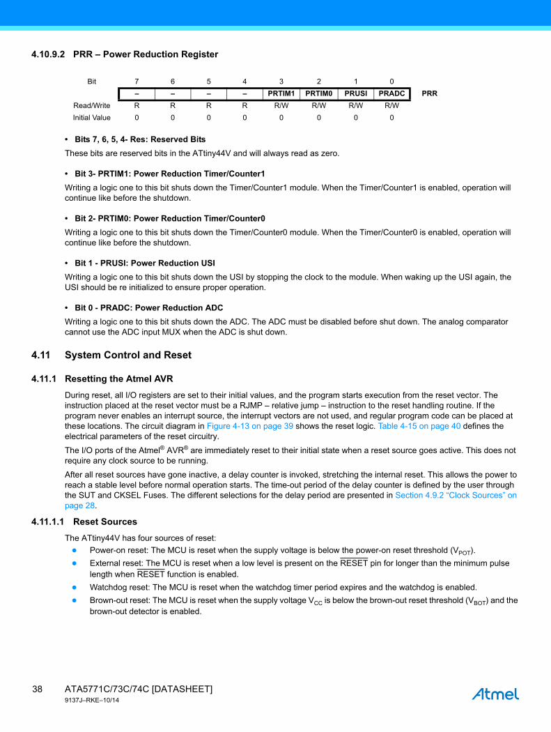
4.10.9.2 PRR – Power Reduction Register
• Bits 7, 6, 5, 4- Res: Reserved Bits
These bits are reserved bits in the ATtiny44V and will always read as zero.
• Bit 3- PRTIM1: Power Reduction Timer/Counter1
Writing a logic one to this bit shuts down the Timer/Counter1 module. When the Timer/Counter1 is enabled, operation will continue like before the shutdown.
• Bit 2- PRTIM0: Power Reduction Timer/Counter0
Writing a logic one to this bit shuts down the Timer/Counter0 module. When the Timer/Counter0 is enabled, operation will continue like before the shutdown.
• Bit 1 - PRUSI: Power Reduction USI
Writing a logic one to this bit shuts down the USI by stopping the clock to the module. When waking up the USI again, the USI should be re initialized to ensure proper operation.
• Bit 0 - PRADC: Power Reduction ADC
Writing a logic one to this bit shuts down the ADC. The ADC must be disabled before shut down. The analog comparator cannot use the ADC input MUX when the ADC is shut down.
4.11 System Control and Reset
4.11.1 Resetting the Atmel AVR
During reset, all I/O registers are set to their initial values, and the program starts execution from the reset vector. The instruction placed at the reset vector must be a RJMP – relative jump – instruction to the reset handling routine. If the program never enables an interrupt source, the interrupt vectors are not used, and regular program code can be placed at these locations. The circuit diagram in Figure 4-13 on page 39 shows the reset logic. Table 4-15 on page 40 defines the electrical parameters of the reset circuitry.
The I/O ports of the Atmel® AVR® are immediately reset to their initial state when a reset source goes active. This does not require any clock source to be running.
After all reset sources have gone inactive, a delay counter is invoked, stretching the internal reset. This allows the power to reach a stable level before normal operation starts. The time-out period of the delay counter is defined by the user through the SUT and CKSEL Fuses. The different selections for the delay period are presented in Section 4.9.2 “Clock Sources” on page 28.
4.11.1.1 Reset Sources
The ATtiny44V has four sources of reset:
● Power-on reset: The MCU is reset when the supply voltage is below the power-on reset threshold (VPOT).
● External reset: The MCU is reset when a low level is present on the RESET pin for longer than the minimum pulse length when RESET function is enabled.
● Watchdog reset: The MCU is reset when the watchdog timer period expires and the watchdog is enabled.
● Brown-out reset: The MCU is reset when the supply voltage VCC is below the brown-out reset threshold (VBOT) and the brown-out detector is enabled.
Bit 7 6 5 4 3 2 1 0
– – – – PRTIM1 PRTIM0 PRUSI PRADC PRR
Read/Write R R R R R/W R/W R/W R/W
Initial Value 0 0 0 0 0 0 0 0
ATA5771C/73C/74C [DATASHEET]9137J–RKE–10/14
38

Figure 4-13. Reset Logic
4.11.1.2 Power-on Reset
A power-on reset (POR) pulse is generated by an on-chip detection circuit. The detection level is defined in Section 8.3.4 “System and Reset Characterizations” on page 164. The POR is activated whenever VCC is below the detection level. The POR circuit can be used to trigger the start-up reset, as well as to detect a failure in supply voltage.
A power-on reset (POR) circuit ensures that the device is reset from power-on. Reaching the power-on reset threshold voltage invokes the delay counter, which determines how long the device is kept in RESET after VCC rise. The RESET signal is activated again, without any delay, when VCC decreases below the detection level.
Power-on ResetCircuit
Brown-outReset Circuit
MCU StatusRegister (MCUSR)
Reset Circuit
Pull-up Resistor
BODLEVEL [1 to 0]
SQ
R
DATA BUS
CK
SUT[1:0]
CKSEL[1:0]C
OU
NTE
R R
ES
ET IN
TER
NA
L R
ES
ET
TIMEOUT
SPIKEFILTERRESET
VCC
Delay Counters
WatchdogTimer
WatchdogOscillator
ClockGenerator
PO
RF
BO
RF
WD
RF
EX
TRF
39ATA5771C/73C/74C [DATASHEET]9137J–RKE–10/14

Figure 4-14. MCU Start-up, RESET Tied to VCC
Figure 4-15. MCU Start-up, RESET Extended Externally
VCC
INTERNALRESET
TIME-OUT
RESET
VPORMAX
VPORMIN
VRST
tTOUT
VTCCRR
VCC
INTERNALRESET
TIME-OUT
RESET
VPOT
VRST
tTOUT
Table 4-15. Power On Reset Specifications
Parameter Symbol Min Typ Max Unit
Power-on reset threshold voltage (rising)VPOT
1.1 1.4 1.7 V
Power-on reset threshold voltage (falling)(1) 0.8 1.3 1.6 V
VCC max. start voltage to ensure internal power-on reset signal VPORMAX 0.4 V
VCC Min. start voltage to ensure internal power-on reset signal VPORMIN -0.1 V
VCC rise rate to ensure power-on reset VCCRR 0.01 V/ms
RESET pin threshold voltage VRST 0.1 VCC 0.9VCC V
Note: 1. Before rising, the supply has to be between VPORMIN and VPORMAX to ensure a reset.
ATA5771C/73C/74C [DATASHEET]9137J–RKE–10/14
40

4.11.1.3 External Reset
An external reset is generated by a low level on the RESET pin if enabled. Reset pulses longer than the minimum pulse width (see Section 8.3.4 “System and Reset Characterizations” on page 164) will generate a reset, even if the clock is not running. Shorter pulses are not guaranteed to generate a reset. When the applied signal reaches the reset threshold voltage – VRST – on its positive edge, the delay counter starts the MCU after the time-out period – tTOUT – has expired.
Figure 4-16. External Reset During Operation
4.11.1.4 Brown-out Detection
The Atmel® ATtiny44V has an on-chip brown-out detection (BOD) circuit for monitoring the VCC level during operation by comparing it to a fixed trigger level. The trigger level for the BOD can be selected by the BODLEVEL Fuses. The trigger level has a hysteresis to ensure spike free brown-out detection. The hysteresis on the detection level should be interpreted as VBOT+ = VBOT + VHYST/2 and VBOT- = VBOT – VHYST/2.
When the BOD is enabled, and VCC decreases to a value below the trigger level (VBOT- in Figure 4-17), the brown-out reset is immediately activated. When VCC increases above the trigger level (VBOT+ in Figure 4-17), the delay counter starts the MCU after the time-out period tTOUT has expired.
The BOD circuit will only detect a drop in VCC if the voltage stays below the trigger level for longer than tBOD given in Section 8.3.4 “System and Reset Characterizations” on page 164.
Figure 4-17. Brown-out Reset During Operation
tTOUT
RESET
VCC
INTERNALRESET
TIME-OUT
VRST
VBOT-
VBOT+
tTOUT
VCC
RESET
INTERNALRESET
TIME-OUT
41ATA5771C/73C/74C [DATASHEET]9137J–RKE–10/14

4.11.1.5 Watchdog Reset
When the watchdog times out, it will generate a short reset pulse of one CK cycle duration. On the falling edge of this pulse, the delay timer starts counting the time-out period tTOUT. See Section 4.11.3 “Watchdog Timer” on page 42 for details on operation of the watchdog timer.
Figure 4-18. Watchdog Reset During Operation
4.11.2 Internal Voltage Reference
The Atmel® ATtiny44V features an internal bandgap reference. This reference is used for brown-out detection, and it can be used as an input to the analog comparator or the ADC.
4.11.2.1 Voltage Reference Enable Signals and Start-up Time
The voltage reference has a start-up time that may influence the way it should be used. The start-up time is given in Section 8.3.4 “System and Reset Characterizations” on page 164. To save power, the reference is not always turned on. The reference is on during the following situations:
1. When the BOD is enabled (by programming the BODLEVEL [2..0] Fuse).
2. When the bandgap reference is connected to the analog comparator (by setting the ACBG bit in ACSR).
3. When the ADC is enabled.
Thus, when the BOD is not enabled, after setting the ACBG bit or enabling the ADC, the user must always allow the reference to start up before the output from the analog comparator or ADC is used. To reduce power consumption in power-down mode, the user can avoid the three conditions above to ensure that the reference is turned off before entering power-down mode.
4.11.3 Watchdog Timer
The watchdog timer is clocked from an on-chip oscillator which runs at 128kHz. By controlling the watchdog timer prescaler, the watchdog reset interval can be adjusted as shown in Table 4-18 on page 45. The WDR – watchdog reset – instruction resets the watchdog timer. The watchdog timer is also reset when it is disabled and when a chip reset occurs. Ten different clock cycle periods can be selected to determine the reset period. If the reset period expires without another watchdog reset, the ATtiny44V resets and executes from the reset vector. For timing details on the watchdog reset, refer to Table 4-18 on page 45.
The watchdog timer can also be configured to generate an interrupt instead of a reset. This can be very helpful when using the watchdog to wake-up from power-down.
To prevent unintentional disabling of the watchdog or unintentional change of time-out period, two different safety levels are selected by the fuse WDTON as shown in Table 4-16 See Section 4.11.4 “Timed Sequences for Changing the Configuration of the Watchdog Timer” on page 43 for details.
VCC
INTERNALRESET
WDTTIME-OUT
RESETTIME-OUT
RESET
tTOUT
1 CK Cycle
ATA5771C/73C/74C [DATASHEET]9137J–RKE–10/14
42
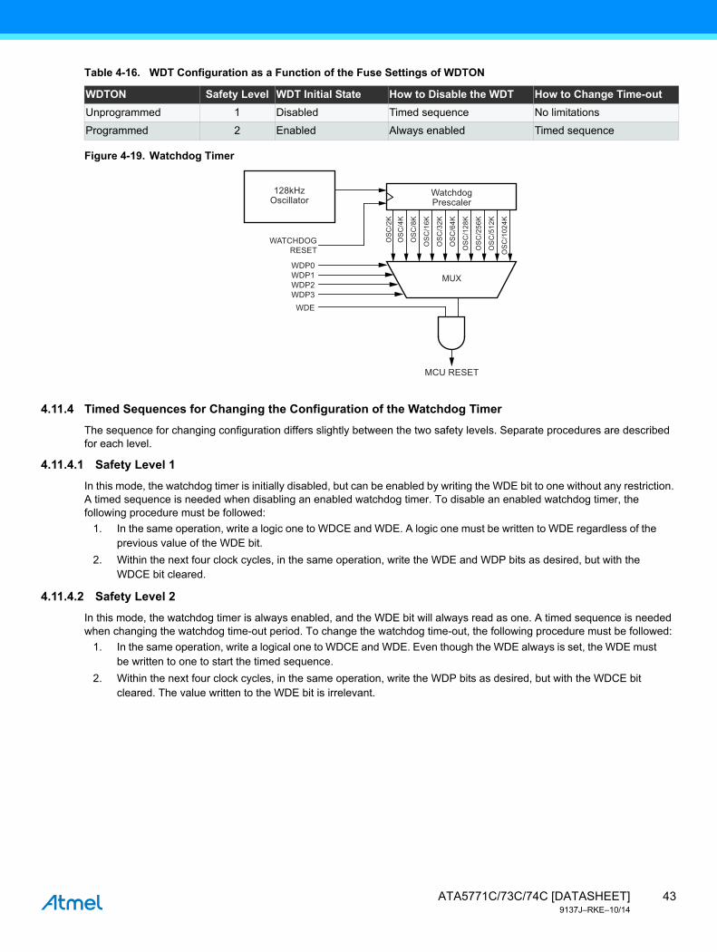
Figure 4-19. Watchdog Timer
4.11.4 Timed Sequences for Changing the Configuration of the Watchdog Timer
The sequence for changing configuration differs slightly between the two safety levels. Separate procedures are described for each level.
4.11.4.1 Safety Level 1
In this mode, the watchdog timer is initially disabled, but can be enabled by writing the WDE bit to one without any restriction. A timed sequence is needed when disabling an enabled watchdog timer. To disable an enabled watchdog timer, the following procedure must be followed:
1. In the same operation, write a logic one to WDCE and WDE. A logic one must be written to WDE regardless of the previous value of the WDE bit.
2. Within the next four clock cycles, in the same operation, write the WDE and WDP bits as desired, but with the WDCE bit cleared.
4.11.4.2 Safety Level 2
In this mode, the watchdog timer is always enabled, and the WDE bit will always read as one. A timed sequence is needed when changing the watchdog time-out period. To change the watchdog time-out, the following procedure must be followed:
1. In the same operation, write a logical one to WDCE and WDE. Even though the WDE always is set, the WDE must be written to one to start the timed sequence.
2. Within the next four clock cycles, in the same operation, write the WDP bits as desired, but with the WDCE bit cleared. The value written to the WDE bit is irrelevant.
Table 4-16. WDT Configuration as a Function of the Fuse Settings of WDTON
WDTON Safety Level WDT Initial State How to Disable the WDT How to Change Time-out
Unprogrammed 1 Disabled Timed sequence No limitations
Programmed 2 Enabled Always enabled Timed sequence
OS
C/2
K
OS
C/4
K
OS
C/8
K
OS
C/1
6K
OS
C/3
2K
OS
C/6
4K
OS
C/1
28K
OS
C/2
56K
OS
C/5
12K
OS
C/1
024K
WatchdogPrescaler
MCU RESET
WDP0
WATCHDOGRESET
WDP1WDP2WDP3
WDE
128kHzOscillator
MUX
43ATA5771C/73C/74C [DATASHEET]9137J–RKE–10/14

4.11.5 Register Description
4.11.5.1 MCUSR – MCU Status Register
The MCU status register provides information on which reset source caused an MCU reset.
• Bits 7..4 – Res: Reserved Bits
These bits are reserved bits in the ATtiny44V and will always read as zero.
• Bit 3 – WDRF: Watchdog Reset Flag
This bit is set if a watchdog reset occurs. The bit is reset by a power-on reset, or by writing a logic zero to the flag.
• Bit 2 – BORF: Brown-out Reset Flag
This bit is set if a brown-out reset occurs. The bit is reset by a power-on reset, or by writing a logic zero to the flag.
• Bit 1 – EXTRF: External Reset Flag
This bit is set if an external reset occurs. The bit is reset by a power-on reset, or by writing a logic zero to the flag.
• Bit 0 – PORF: Power-on Reset Flag
This bit is set if a power-on reset occurs. The bit is reset only by writing a logic zero to the flag.
To make use of the reset flags to identify a reset condition, the user should read and then reset the MCUSR as early as possible in the program. If the register is cleared before another reset occurs, the source of the reset can be found by examining the reset flags.
4.11.5.2 WDTCSR – Watchdog Timer Control and Status Register
• Bit 7 – WDIF: Watchdog Timeout Interrupt Flag
This bit is set when a time-out occurs in the watchdog timer and the watchdog timer is configured for interrupt. WDIF is cleared by hardware when executing the corresponding interrupt handling vector. Alternatively, WDIF is cleared by writing a logic one to the flag. When the I-bit in SREG and WDIE are set, the watchdog time-out Interrupt is executed.
• Bit 6 – WDIE: Watchdog Timeout Interrupt Enable
When this bit is written to one, WDE is cleared, and the I-bit in the status register is set, the watchdog time-out interrupt is enabled. In this mode the corresponding interrupt is executed instead of a reset if a timeout in the watchdog timer occurs.
If WDE is set, WDIE is automatically cleared by hardware when a time-out occurs. This is useful for keeping the watchdog Reset security while using the interrupt. After the WDIE bit is cleared, the next time-out will generate a reset. To avoid the watchdog reset, WDIE must be set after each interrupt.
Bit 7 6 5 4 3 2 1 0
0x34 (0x54) – – – – WDRF BORF EXTRF PORF MCUSR
Read/Write R R R R R/W R/W R/W R/W
Initial Value 0 0 0 0 See Bit Description
Bit 7 6 5 4 3 2 1 0
0x21 (0x41) WDIF WDIE WDP3 WDCE WDE WDP2 WDP1 WDP0 WDTCSR
Read/Write R/W R/W R/W R/W R/W R/W R/W R/W
Initial Value 0 0 0 0 X 0 0 0
Table 4-17. Watchdog Timer Configuration
WDE WDIE Watchdog Timer State Action on Time-out
0 0 Stopped None
0 1 Running Interrupt
1 0 Running Reset
1 1 Running Interrupt
ATA5771C/73C/74C [DATASHEET]9137J–RKE–10/14
44

• Bit 4 – WDCE: Watchdog Change Enable
This bit must be set when the WDE bit is written to logic zero. Otherwise, the watchdog will not be disabled. Once written to one, hardware will clear this bit after four clock cycles. See the description of the WDE bit for a watchdog disable procedure. This bit must also be set when changing the prescaler bits. See Section 4.11.4 “Timed Sequences for Changing the Configuration of the Watchdog Timer” on page 43.
• Bit 3 – WDE: Watchdog Enable
When the WDE is written to logic one, the watchdog timer is enabled, and if the WDE is written to logic zero, the watchdog timer function is disabled. WDE can only be cleared if the WDCE bit has logic level one. To disable an enabled watchdog timer, the following procedure must be followed:
1. In the same operation, write a logic one to WDCE and WDE. A logic one must be written to WDE even though it is set to one before the disable operation starts.
2. Within the next four clock cycles, write a logic 0 to WDE. This disables the watchdog.
In safety level 2, it is not possible to disable the watchdog timer, even with the algorithm described above. See Section 4.11.4 “Timed Sequences for Changing the Configuration of the Watchdog Timer” on page 43.
In safety level 1, WDE is overridden by WDRF in MCUSR. See Section 4.11.5.1 “MCUSR – MCU Status Register” on page 44 for description of WDRF. This means that WDE is always set when WDRF is set. To clear WDE, WDRF must be cleared before disabling the Watchdog with the procedure described above. This feature ensures multiple resets during conditions causing failure, and a safe start-up after the failure.
Note: If the watchdog timer is not going to be used in the application, it is important to go through a watchdog disable procedure in the initialization of the device. If the Watchdog is accidentally enabled, for example by a runaway pointer or brown-out condition, the device will be reset, which in turn will lead to a new watchdog reset. To avoid this situation, the application software should always clear the WDRF flag and the WDE control bit in the initialization routine.
• Bits 5, 2..0 – WDP3..0: Watchdog Timer Prescaler 3, 2, 1, and 0
The WDP3..0 bits determine the watchdog timer prescaling when the watchdog timer is enabled. The different prescaling values and their corresponding timeout periods are shown in Table 4-18 on page 45.
Table 4-18. Watchdog Timer Prescale Select
WDP3 WDP2 WDP1 WDP0 Number of WDT Oscillator CyclesTypical Time-out at
VCC = 5.0V
0 0 0 0 2K cycles 16ms
0 0 0 1 4K cycles 32ms
0 0 1 0 8K cycles 64ms
0 0 1 1 16K cycles 0.125s
0 1 0 0 32K cycles 0.25s
0 1 0 1 64K cycles 0.5s
0 1 1 0 128K cycles 1.0s
0 1 1 1 256K cycles 2.0s
1 0 0 0 512K cycles 4.0s
1 0 0 1 1024K cycles 8.0s
1 0 1 0
Reserved
1 0 1 1
1 1 0 0
1 1 0 1
1 1 1 0
1 1 1 1
45ATA5771C/73C/74C [DATASHEET]9137J–RKE–10/14
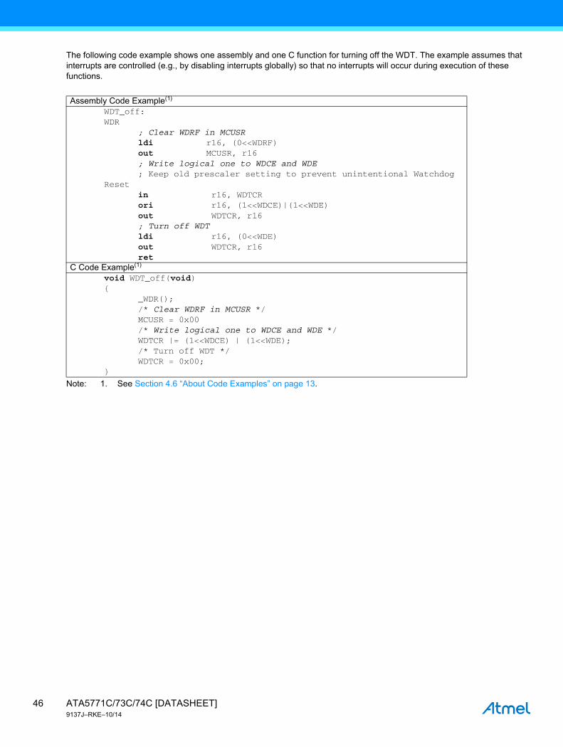
The following code example shows one assembly and one C function for turning off the WDT. The example assumes that interrupts are controlled (e.g., by disabling interrupts globally) so that no interrupts will occur during execution of these functions.
Note: 1. See Section 4.6 “About Code Examples” on page 13.
Assembly Code Example(1)
WDT_off:WDR
; Clear WDRF in MCUSRldi r16, (0<<WDRF)out MCUSR, r16; Write logical one to WDCE and WDE; Keep old prescaler setting to prevent unintentional Watchdog
Resetin r16, WDTCRori r16, (1<<WDCE)|(1<<WDE)out WDTCR, r16; Turn off WDTldi r16, (0<<WDE)out WDTCR, r16ret
C Code Example(1)
void WDT_off(void){
_WDR();/* Clear WDRF in MCUSR */MCUSR = 0x00/* Write logical one to WDCE and WDE */WDTCR |= (1<<WDCE) | (1<<WDE);/* Turn off WDT */WDTCR = 0x00;
}
ATA5771C/73C/74C [DATASHEET]9137J–RKE–10/14
46

4.12 Interrupts
This section describes the specifics of the interrupt handling as performed in Atmel® ATtiny44V. For a general explanation of the AVR interrupt handling, see Section 4.7.8 “Reset and Interrupt Handling” on page 19.
4.12.1 Interrupt Vectors
Table 4-19. Reset and Interrupt Vectors
Vector No. Program Address Source Interrupt Definition
1 0x0000 RESETExternal pin, power-on reset, Brown-out reset, watchdog reset
2 0x0001 INT0 External interrupt request 0
3 0x0002 PCINT0 Pin change interrupt request 0
4 0x0003 PCINT1 Pin change interrupt request 1
5 0x0004 WDT Watchdog time-out
6 0x0005 TIMER1 CAPT Timer/Counter1 capture event
7 0x0006 TIMER1 COMPA Timer/Counter1 compare match A
8 0x0007 TIMER1 COMPB Timer/Counter1 compare match B
9 0x0008 TIMER1 OVF Timer/Counter0 overflow
10 0x0009 TIMER0 COMPA Timer/Counter0 compare match A
11 0x000A TIMER0 COMPB Timer/Counter0 compare match B
12 0x000B TIMER0 OVF Timer/Counter0 overflow
13 0x000C ANA_COMP Analog comparator
14 0x000D ADC ADC conversion complete
15 0x000E EE_RDY EEPROM ready
16 0x000F USI_START USI START
17 0x0010 USI_OVF USI overflow
47ATA5771C/73C/74C [DATASHEET]9137J–RKE–10/14

If the program never enables an interrupt source, the interrupt vectors are not used, and regular program code can be placed at these locations. The most typical and general program setup for the reset and interrupt vector addresses in ATtiny44V is:
Address Labels Code Comments0x0000 rjmp RESET ; Reset Handler0x0001 rjmp EXT_INT0 ; IRQ0 Handler0x0002 rjmp PCINT0 ; PCINT0 Handler0x0003 rjmp PCINT1 ; PCINT1 Handler0x0004 rjmp WATCHDOG ; Watchdog Interrupt Handler0x0005 rjmp TIM1_CAPT ; Timer1 Capture Handler0x0006 rjmp TIM1_COMPA ; Timer1 Compare A Handler0x0007 rjmp TIM1_COMPB ; Timer1 Compare B Handler0x0008 rjmp TIM1_OVF ; Timer1 Overflow Handler0x0009 rjmp TIM0_COMPA ; Timer0 Compare A Handler0x000A rjmp TIM0_COMPB ; Timer0 Compare B Handler0x000B rjmp TIM0_OVF ; Timer0 Overflow Handler0x000C rjmp ANA_COMP ; Analog Comparator Handler0x000D rjmp ADC ; ADC Conversion Handler0x000E rjmp EE_RDY ; EEPROM Ready Handler0x000F rjmp USI_STR ; USI STart Handler0x0010 rjmp USI_OVF ; USI Overflow Handler;0x0011 RESET: ldi r16, high(RAMEND) ; Main program start0x0012 out SPH,r16 ; Set Stack Pointer to top of RAM0x0013 ldi r16, low(RAMEND)0x0014 out SPL,r160x0015 sei ; Enable interrupts0x0016 <instr> xxx... ... ... ...
4.13 External Interrupts
The external interrupts are triggered by the INT0 pin or any of the PCINT11..0 pins. Observe that, if enabled, the interrupts will trigger even if the INT0 or PCINT11..0 pins are configured as outputs. This feature provides a way of generating a software interrupt. Pin change 0 interrupts PCI0 will trigger if any enabled PCINT7..0 pin toggles. Pin change 1 interrupts PCI1 will trigger if any enabled PCINT11..8 pin toggles. The PCMSK0 and PCMSK1 registers control which pins contribute to the pin change interrupts. Pin change interrupts on PCINT11..0 are detected asynchronously. This implies that these interrupts can be used for waking the part also from sleep modes other than idle mode.
The INT0 interrupts can be triggered by a falling or rising edge or a low level. This is set up as indicated in the specification for the MCU control register – MCUCR. When the INT0 interrupt is enabled and is configured as level triggered, the interrupt will trigger as long as the pin is held low. Note that recognition of falling or rising edge interrupts on INT0 requires the presence of an I/O clock, described in Section 4.9.1 “Clock Systems and their Distribution” on page 27. Low level interrupt on INT0 is detected asynchronously. This implies that this interrupt can be used for waking the part also from sleep modes other than Idle mode. The I/O clock is halted in all sleep modes except Idle mode.
Note that if a level triggered interrupt is used for wake-up from power-down, the required level must be held long enough for the MCU to complete the wake-up to trigger the level interrupt. If the level disappears before the end of the start-up time, the MCU will still wake up, but no interrupt will be generated. The start-up time is defined by the SUT and CKSEL fuses as described in Section 4.9 “System Clock and Clock Options” on page 27.
ATA5771C/73C/74C [DATASHEET]9137J–RKE–10/14
48
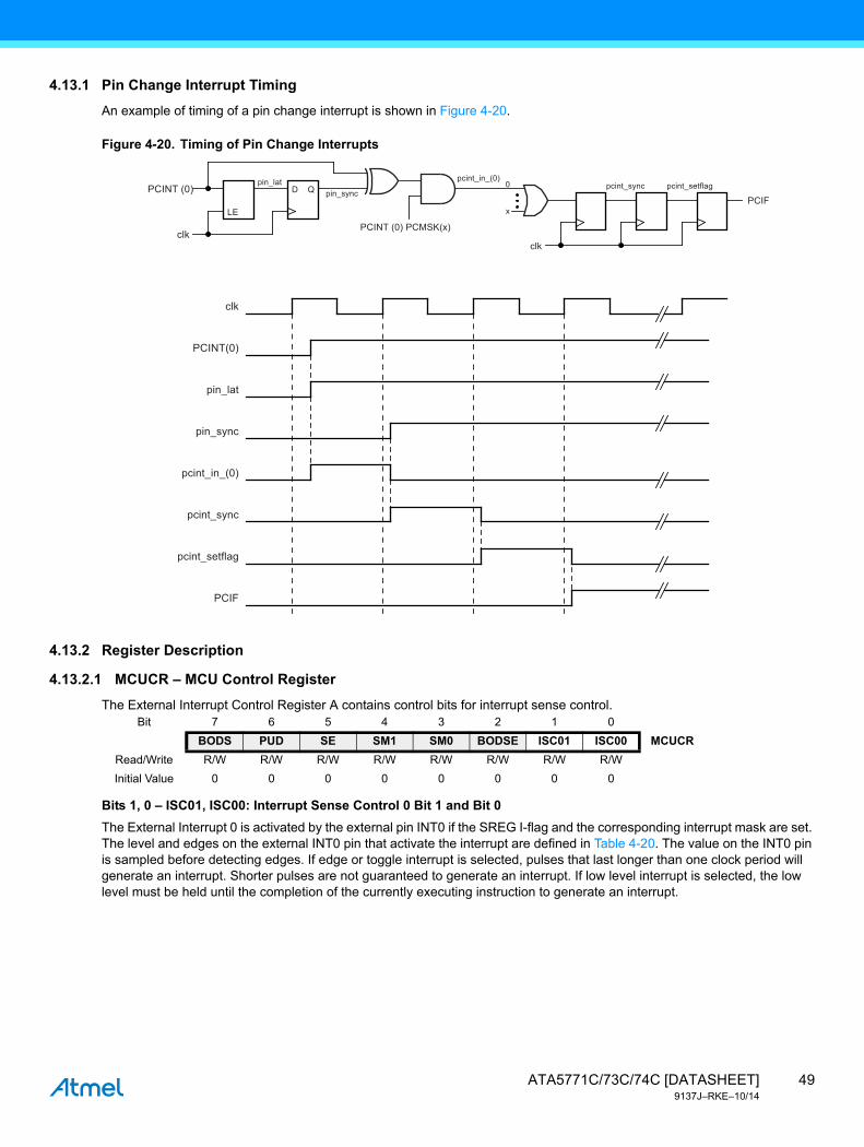
4.13.1 Pin Change Interrupt Timing
An example of timing of a pin change interrupt is shown in Figure 4-20.
Figure 4-20. Timing of Pin Change Interrupts
4.13.2 Register Description
4.13.2.1 MCUCR – MCU Control Register
The External Interrupt Control Register A contains control bits for interrupt sense control.
Bits 1, 0 – ISC01, ISC00: Interrupt Sense Control 0 Bit 1 and Bit 0
The External Interrupt 0 is activated by the external pin INT0 if the SREG I-flag and the corresponding interrupt mask are set. The level and edges on the external INT0 pin that activate the interrupt are defined in Table 4-20. The value on the INT0 pin is sampled before detecting edges. If edge or toggle interrupt is selected, pulses that last longer than one clock period will generate an interrupt. Shorter pulses are not guaranteed to generate an interrupt. If low level interrupt is selected, the low level must be held until the completion of the currently executing instruction to generate an interrupt.
clk
pin_lat
pin_sync
PCINT(0)
pcint_in_(0)
pcint_sync
pcint_setflag
PCIF
pin_latpin_sync
pcint_sync
clk
x
0
clk
pcint_setflag
PCINT (0) PCMSK(x)
PCINT (0)PCIF
pcint_in_(0)
LE
D Q
Bit 7 6 5 4 3 2 1 0
BODS PUD SE SM1 SM0 BODSE ISC01 ISC00 MCUCR
Read/Write R/W R/W R/W R/W R/W R/W R/W R/W
Initial Value 0 0 0 0 0 0 0 0
49ATA5771C/73C/74C [DATASHEET]9137J–RKE–10/14

4.13.2.2 GIMSK – General Interrupt Mask Register
• Bits 7, 3..0 – Res: Reserved Bits
These bits are reserved bits in the ATtiny44V and will always read as zero.
• Bit 6 – INT0: External Interrupt Request 0 Enable
When the INT0 bit is set (one) and the I-bit in the status register (SREG) is set (one), the external pin interrupt is enabled. The interrupt sense control0 bits 1/0 (ISC01 and ISC00) in the external interrupt control register A (EICRA) define whether the external interrupt is activated on rising and/or falling edge of the INT0 pin or level sensed. Activity on the pin will cause an interrupt request even if INT0 is configured as an output. The corresponding interrupt of external interrupt request 0 is executed from the INT0 Interrupt Vector.
• Bit 5 – PCIE1: Pin Change Interrupt Enable 1
When the PCIE1 bit is set (one) and the I-bit in the status register (SREG) is set (one), pin change interrupt 1 is enabled. Any change on any enabled PCINT11..8 pin will cause an interrupt. The corresponding interrupt of pin change interrupt request is executed from the PCI1 interrupt vector. PCINT11..8 pins are enabled individually by the PCMSK1 register.
• Bit 4– PCIE0: Pin Change Interrupt Enable 0
When the PCIE0 bit is set (one) and the I-bit in the status register (SREG) is set (one), pin change interrupt 0 is enabled. Any change on any enabled PCINT7..0 pin will cause an interrupt. The corresponding interrupt of pin change interrupt request is executed from the PCI0 interrupt vector. PCINT7..0 pins are enabled individually by the PCMSK0 register.
4.13.2.3 GIFR – General Interrupt Flag Register
• Bits 7, 3..0 – Res: Reserved Bits
These bits are reserved bits in the ATtiny44V and will always read as zero.
• Bit 6 – INTF0: External Interrupt Flag 0
When an edge or logic change on the INT0 pin triggers an interrupt request, INTF0 becomes set (one). If the I-bit in SREG and the INT0 bit in GIMSK are set (one), the MCU will jump to the corresponding Interrupt Vector. The flag is cleared when the interrupt routine is executed. Alternatively, the flag can be cleared by writing a logical one to it. This flag is always cleared when INT0 is configured as a level interrupt.
Table 4-20. Interrupt 0 Sense Control
ISC01 ISC00 Description
0 0 The low level of INT0 generates an interrupt request.
0 1 Any logical change on INT0 generates an interrupt request.
1 0 The falling edge of INT0 generates an interrupt request.
1 1 The rising edge of INT0 generates an interrupt request.
Bit 7 6 5 4 3 2 1 0
0x3B (0x5B) – INT0 PCIE1 PCIE0 – – – – GIMSK
Read/Write R R/W R/W R/w R R R R
Initial Value 0 0 0 0 0 0 0 0
Bit 7 6 5 4 3 2 1 0
0x3A (0x5A) – INTF0 PCIF1 PCIF0 – – – – GIFR
Read/Write R R/W R/W R/W R R R R
Initial Value 0 0 0 0 0 0 0 0
ATA5771C/73C/74C [DATASHEET]9137J–RKE–10/14
50

• Bit 5 – PCIF1: Pin Change Interrupt Flag 1
When a logic change on any PCINT11..8 pin triggers an interrupt request, PCIF1 becomes set (one). If the I-bit in SREG and the PCIE1 bit in GIMSK are set (one), the MCU will jump to the corresponding Interrupt Vector. The flag is cleared when the interrupt routine is executed. Alternatively, the flag can be cleared by writing a logical one to it.
• Bit 4– PCIF0: Pin Change Interrupt Flag 0
When a logic change on any PCINT7..0 pin triggers an interrupt request, PCIF becomes set (one). If the I-bit in SREG and the PCIE0 bit in GIMSK are set (one), the MCU will jump to the corresponding Interrupt vector. The flag is cleared when the interrupt routine is executed. Alternatively, the flag can be cleared by writing a logical one to it.
4.13.2.4 PCMSK1 – Pin Change Mask Register 1
• Bits 7, 4– Res: Reserved Bits
These bits are reserved bits in the ATtiny44V and will always read as zero.
• Bits 3..0 – PCINT11..8: Pin Change Enable Mask 11..8
Each PCINT11..8 bit selects whether pin change interrupt is enabled on the corresponding I/O pin. If PCINT11..8 is set and the PCIE1 bit in GIMSK is set, pin change interrupt is enabled on the corresponding I/O pin. If PCINT11..8 is cleared, pin change interrupt on the corresponding I/O pin is disabled.
4.13.2.5 PCMSK0 – Pin Change Mask Register 0
• Bits 7..0 – PCINT7..0: Pin Change Enable Mask 7..0
Each PCINT7..0 bit selects whether pin change interrupt is enabled on the corresponding I/O pin. If PCINT7..0 is set and the PCIE0 bit in GIMSK is set, pin change interrupt is enabled on the corresponding I/O pin. If PCINT7..0 is cleared, pin change interrupt on the corresponding I/O pin is disabled.
Bit 7 6 5 4 3 2 1 0
0x20 (0x40) – – – – PCINT11 PCINT10 PCINT9 PCINT8 PCMSK1
Read/Write R R R R R/W R/W R/W R/W
Initial Value 0 0 0 0 0 0 0 0
Bit 7 6 5 4 3 2 1 0
0x12 (0x32) PCINT7 PCINT6 PCINT5 PCINT4 PCINT3 PCINT2 PCINT1 PCINT0 PCMSK0
Read/Write R/W R/W R/W R/W R/W R/W R/W R/W
Initial Value 0 0 0 0 0 0 0 0
51ATA5771C/73C/74C [DATASHEET]9137J–RKE–10/14

4.14 I/O Ports
4.14.1 Overview
All AVR® ports have true read-modify-write functionality when used as general digital I/O ports. This means that the direction of one port pin can be changed without unintentionally changing the direction of any other pin with the SBI and CBI instructions. The same applies when changing drive value (if configured as output) or enabling/disabling of pull-up resistors (if configured as input). Each output buffer has symmetrical drive characteristics with both high sink and source capability. The pin driver is strong enough to drive LED displays directly. All port pins have individually selectable pull-up resistors with a supply-voltage invariant resistance. All I/O pins have protection diodes to both VCC and ground as indicated in Figure 4-21. See Section 8. “Electrical Characteristics” on page 160 for a complete list of parameters.
Figure 4-21. I/O Pin Equivalent Schematic
All registers and bit references in this section are written in general form. A lower case “x” represents the numbering letter for the port, and a lower case “n” represents the bit number. However, when using the register or bit defines in a program, the precise form must be used. For example, PORTB3 for bit no. 3 in Port B, here documented generally as PORTxn. The physical I/O registers and bit locations are listed in Table 4-29.
Three I/O memory address locations are allocated for each port, one each for the data register – PORTx, data direction register – DDRx, and the port input pins – PINx. The port input pins I/O location is read only, while the data register and the data direction register are read/write. However, writing a logic one to a bit in the PINx register, will result in a toggle in the corresponding bit in the data register. In addition, the pull-up disable – PUD bit in MCUCR disables the pull-up function for all pins in all ports when set.
Using the I/O port as general digital I/O is described in Section 4.14.2 “Ports as General Digital I/O” on page 53. Most port pins are multiplexed with alternate functions for the peripheral features on the device. How each alternate function interferes with the port pin is described in Section 4.14.3 “Alternate Port Functions” on page 57. Refer to the individual module sections for a full description of the alternate functions.
Note that enabling the alternate function of some of the port pins does not affect the use of the other pins in the port as general digital I/O.
Cpin
Rpu
PxnLogic
See Figure”General Digital I/O”
for Details
ATA5771C/73C/74C [DATASHEET]9137J–RKE–10/14
52

4.14.2 Ports as General Digital I/O
The ports are bi-directional I/O ports with optional internal pull-ups. Figure 4-22 shows a functional description of one I/O-port pin, here generically called Pxn.
Figure 4-22. General Digital I/O(1)
Note: 1. WRx, WPx, WDx, RRx, RPx, and RDx are common to all pins within the same port. clkI/O, SLEEP, and PUD are common to all ports.
4.14.2.1 Configuring the Pin
Each port pin consists of three register bits: DDxn, PORTxn, and PINxn. As shown in Table 4-29 on page 64, the DDxn bits are accessed at the DDRx I/O address, the PORTxn bits at the PORTx I/O address, and the PINxn bits at the PINx I/O address.
The DDxn bit in the DDRx Register selects the direction of this pin. If DDxn is written logic one, Pxn is configured as an output pin. If DDxn is written logic zero, Pxn is configured as an input pin.
If PORTxn is written logic one when the pin is configured as an input pin, the pull-up resistor is activated. To switch the pull-up resistor off, PORTxn has to be written logic zero or the pin has to be configured as an output pin. The port pins are tri-stated when reset condition becomes active, even if no clocks are running.
If PORTxn is written logic one when the pin is configured as an output pin, the port pin is driven high (one). If PORTxn is written logic zero when the pin is configured as an output pin, the port pin is driven low (zero).
D0
1
Q
WRxRRx
WPx
Pnx
CLR
RESET
Synchronizer
DAT
A B
US
PORTxn
Q
Q
L
D
Q
QD
Q
PINxn
RESET
RPx
WDx: WRITE DDRx
WRx:
WPx:RPx:RRx: READ PORTx REGISTER
READ PORTx PINWRITE PORTx REGISTER
RDx:WRITE PORTxREAD DDRx
PUD: PULLUP DISABLE
CLKI/O:SLEEP:
I/O CLOCKSLEEP CONTROL
RDx
CLKI/O
PUD
WDx
SLEEP
D
Q CLR
DDxn
Q
53ATA5771C/73C/74C [DATASHEET]9137J–RKE–10/14

4.14.2.2 Toggling the Pin
Writing a logic one to PINxn toggles the value of PORTxn, independent on the value of DDRxn. Note that the SBI instruction can be used to toggle one single bit in a port.
4.14.2.3 Switching Between Input and Output
When switching between tri-state ({DDxn, PORTxn} = 0b00) and output high ({DDxn, PORTxn} = 0b11), an intermediate state with either pull-up enabled {DDxn, PORTxn} = 0b01) or output low ({DDxn, PORTxn} = 0b10) must occur. Normally, the pull-up enabled state is fully acceptable, as a high-impedant environment will not notice the difference between a strong high driver and a pull-up. If this is not the case, the PUD bit in the MCUCR register can be set to disable all pull-ups in all ports.
Switching between input with pull-up and output low generates the same problem. The user must use either the tri-state ({DDxn, PORTxn} = 0b00) or the output high state ({DDxn, PORTxn} = 0b10) as an intermediate step.
Table 4-21 summarizes the control signals for the pin value.
4.14.2.4 Reading the Pin Value
Independent of the setting of data direction bit DDxn, the port pin can be read through the PINxn register bit. As shown in Figure 4-22 on page 53, the PINxn register bit and the preceding latch constitute a synchronizer. This is needed to avoid metastability if the physical pin changes value near the edge of the internal clock, but it also introduces a delay. Figure 4-23 shows a timing diagram of the synchronization when reading an externally applied pin value. The maximum and minimum propagation delays are denoted tpd,max and tpd,min respectively.
Figure 4-23. Synchronization when Reading an Externally Applied Pin Value
Consider the clock period starting shortly after the first falling edge of the system clock. The latch is closed when the clock is low, and goes transparent when the clock is high, as indicated by the shaded region of the “SYNC LATCH” signal. The signal value is latched when the system clock goes low. It is clocked into the PINxn register at the succeeding positive clock edge. As indicated by the two arrows tpd,max and tpd,min, a single signal transition on the pin will be delayed between ½ and 1½ system clock period depending upon the time of assertion.
Table 4-21. Port Pin Configurations
DDxn PORTxnPUD
(in MCUCR) I/O Pull-up Comment
0 0 X Input No Tri-state (Hi-Z)
0 1 0 Input Yes Pxn will source current if ext. pulled low
0 1 1 Input No Tri-state (Hi-Z)
1 0 X Output No Output low (sink)
1 1 X Output No Output high (source)
tpd,max
tpd,min
0xFF0x00
XXX in r17,PINxXXXINSTRUCTIONS
SYNC LATCH
r17
PINxn
SYSTEM CLK
ATA5771C/73C/74C [DATASHEET]9137J–RKE–10/14
54
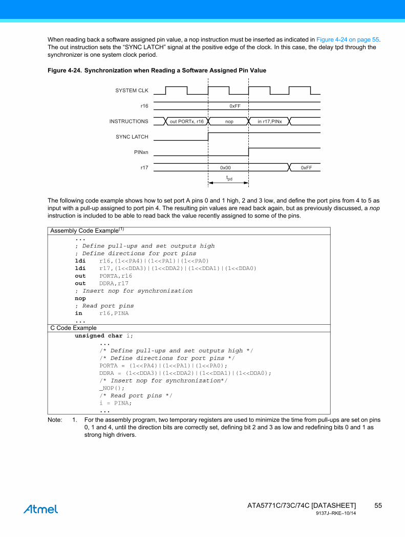
When reading back a software assigned pin value, a nop instruction must be inserted as indicated in Figure 4-24 on page 55. The out instruction sets the “SYNC LATCH” signal at the positive edge of the clock. In this case, the delay tpd through the synchronizer is one system clock period.
Figure 4-24. Synchronization when Reading a Software Assigned Pin Value
The following code example shows how to set port A pins 0 and 1 high, 2 and 3 low, and define the port pins from 4 to 5 as input with a pull-up assigned to port pin 4. The resulting pin values are read back again, but as previously discussed, a nop instruction is included to be able to read back the value recently assigned to some of the pins.
Note: 1. For the assembly program, two temporary registers are used to minimize the time from pull-ups are set on pins 0, 1 and 4, until the direction bits are correctly set, defining bit 2 and 3 as low and redefining bits 0 and 1 as strong high drivers.
Assembly Code Example(1)
...; Define pull-ups and set outputs high; Define directions for port pinsldi r16,(1<<PA4)|(1<<PA1)|(1<<PA0)ldi r17,(1<<DDA3)|(1<<DDA2)|(1<<DDA1)|(1<<DDA0)out PORTA,r16out DDRA,r17; Insert nop for synchronizationnop; Read port pinsin r16,PINA...
C Code Exampleunsigned char i;
.../* Define pull-ups and set outputs high *//* Define directions for port pins */PORTA = (1<<PA4)|(1<<PA1)|(1<<PA0);DDRA = (1<<DDA3)|(1<<DDA2)|(1<<DDA1)|(1<<DDA0);/* Insert nop for synchronization*/_NOP();/* Read port pins */i = PINA;...
tpd
0xFF
0xFF
0x00
nop in r17,PINxout PORTx, r16INSTRUCTIONS
SYNC LATCH
r16
r17
PINxn
SYSTEM CLK
55ATA5771C/73C/74C [DATASHEET]9137J–RKE–10/14

4.14.2.5 Digital Input Enable and Sleep Modes
As shown in Figure 4-22 on page 53, the digital input signal can be clamped to ground at the input of the schmitt-trigger. The signal denoted SLEEP in the figure, is set by the MCU sleep controller in power-down mode, power-save mode, and standby mode to avoid high power consumption if some input signals are left floating, or have an analog signal level close to VCC/2.
SLEEP is overridden for port pins enabled as external interrupt pins. If the external interrupt request is not enabled, SLEEP is active also for these pins. SLEEP is also overridden by various other alternate functions as described in Section 4.14.3 “Alternate Port Functions” on page 57.
If a logic high level (“one”) is present on an asynchronous external interrupt pin configured as “Interrupt on Rising Edge, Falling Edge, or Any Logic Change on Pin” while the external interrupt is not enabled, the corresponding external interrupt flag will be set when resuming from the above mentioned sleep mode, as the clamping in these sleep mode produces the requested logic change.
4.14.2.6 Unconnected Pins
If some pins are unused, it is recommended to ensure that these pins have a defined level. Even though most of the digital inputs are disabled in the deep sleep modes as described above, floating inputs should be avoided to reduce current consumption in all other modes where the digital inputs are enabled (reset, active mode and idle mode).
The simplest method to ensure a defined level of an unused pin, is to enable the internal pull-up. In this case, the pull-up will be disabled during reset. If low power consumption during reset is important, it is recommended to use an external pull-up or pulldown. Connecting unused pins directly to VCC or GND is not recommended, since this may cause excessive currents if the pin is accidentally configured as an output.
ATA5771C/73C/74C [DATASHEET]9137J–RKE–10/14
56

4.14.3 Alternate Port Functions
Most port pins have alternate functions in addition to being general digital I/Os. Figure 4-25 shows how the port pin control signals from the simplified Figure 4-22 on page 53 can be overridden by alternate functions. The overriding signals may not be present in all port pins, but the figure serves as a generic description applicable to all port pins in the AVR® microcontroller family.
Figure 4-25. Alternate Port Functions(1)
Note: 1. WRx, WPx, WDx, RRx, RPx, and RDx are common to all pins within the same port. clkI/O, SLEEP, and PUD are common to all ports. All other signals are unique for each pin.
D0
1
Q
WRxRRx
WPx
PTOExn
Pnx
CLR
CLR CLR
RESET
Synchronizer
DAT
A B
US
PORTxn
Q
0
1
Q
L
D
Q
QD
Q
PINxn
0
1
RESET
RPx
Pxn PULL-UP OVERRIDE ENABLEPxn PULL-UP OVERRIDE VALUE
PUD: PULL-UP DISABLEPUOExn:
Pxn PORT VALUE OVERRIDE VALUEPVOVxn:Pxn PORT VALUE OVERRIDE ENABLEPVOExn:
Pxn DATA DIRECTION OVERRIDE ENABLEPxn DATA DIRECTION OVERRIDE VALUE
DDOExn:DDOVxn:
SLEEP CONTROLSLEEP:Pxn, PORT TOGGLE OVERRIDE ENABLEPTOExn:
Pxn DIGITAL INPUT ENABLE OVERRIDE VALUEDIEOVxn:Pxn DIGITAL INPUT ENABLE OVERRIDE ENABLEDIEOExn:
I/O CLOCK
RDx:
RPx:WRITE PINx
WRx:
ANALOG INPUT/OUTPUT PIN n ON PORTxDIGITAL INPUT PIN n ON PORTx
RRx: READ PORTx REGISTER
WPx:
WRITE PORTx
AIOxn:DIxn:
READ PORTx PIN
WDx:READ DDRxWRITE DDRxPUOVxn:
RDx
CLKI/O
DIxnAIOxn
CLK:I/O
DIEOVxn
DIEOExn
PVOExn
DDOExn
PVOVxn
0
1
PUOExn
PUOVxn
0
1 DDOVxn
SLEEP
PUD
WDx
D
Q CLR
DDxn
Q
57ATA5771C/73C/74C [DATASHEET]9137J–RKE–10/14
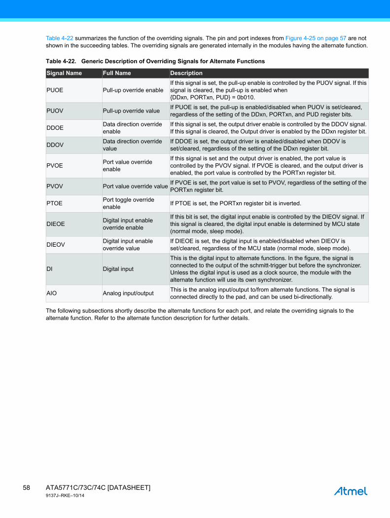
Table 4-22 summarizes the function of the overriding signals. The pin and port indexes from Figure 4-25 on page 57 are not shown in the succeeding tables. The overriding signals are generated internally in the modules having the alternate function.
The following subsections shortly describe the alternate functions for each port, and relate the overriding signals to the alternate function. Refer to the alternate function description for further details.
Table 4-22. Generic Description of Overriding Signals for Alternate Functions
Signal Name Full Name Description
PUOE Pull-up override enableIf this signal is set, the pull-up enable is controlled by the PUOV signal. If this signal is cleared, the pull-up is enabled when {DDxn, PORTxn, PUD} = 0b010.
PUOV Pull-up override valueIf PUOE is set, the pull-up is enabled/disabled when PUOV is set/cleared, regardless of the setting of the DDxn, PORTxn, and PUD register bits.
DDOEData direction override enable
If this signal is set, the output driver enable is controlled by the DDOV signal. If this signal is cleared, the Output driver is enabled by the DDxn register bit.
DDOVData direction override value
If DDOE is set, the output driver is enabled/disabled when DDOV is set/cleared, regardless of the setting of the DDxn register bit.
PVOEPort value override enable
If this signal is set and the output driver is enabled, the port value is controlled by the PVOV signal. If PVOE is cleared, and the output driver is enabled, the port value is controlled by the PORTxn register bit.
PVOV Port value override valueIf PVOE is set, the port value is set to PVOV, regardless of the setting of the PORTxn register bit.
PTOEPort toggle override enable
If PTOE is set, the PORTxn register bit is inverted.
DIEOEDigital input enable override enable
If this bit is set, the digital input enable is controlled by the DIEOV signal. If this signal is cleared, the digital input enable is determined by MCU state (normal mode, sleep mode).
DIEOVDigital input enable override value
If DIEOE is set, the digital input is enabled/disabled when DIEOV is set/cleared, regardless of the MCU state (normal mode, sleep mode).
DI Digital input
This is the digital input to alternate functions. In the figure, the signal is connected to the output of the schmitt-trigger but before the synchronizer. Unless the digital input is used as a clock source, the module with the alternate function will use its own synchronizer.
AIO Analog input/outputThis is the analog input/output to/from alternate functions. The signal is connected directly to the pad, and can be used bi-directionally.
ATA5771C/73C/74C [DATASHEET]9137J–RKE–10/14
58

4.14.3.1 Alternate Functions of Port A
The Port A pins with alternate function are shown in Table 4-27 on page 62.
• Port A, Bit 0 – ADC0/AREF/PCINT0
ADC0: Analog to digital converter, channel 0.
AREF: External analog reference for ADC. Pullup and output driver are disabled on PA0 when the pin is used as an external reference or internal voltage reference with external capacitor at the AREF pin by setting (one) the bit REFS0 in the ADC multiplexer selection register (ADMUX).
PCINT0: pin change interrupt source 0. The PA0 pin can serve as an external interrupt source for pin change interrupt 0.
Table 4-23. Port A Pins Alternate Functions
Port Pin Alternate Function
PA0
ADC0: ADC input channel 0.
AREF: External analog reference.
PCINT0: Pin change interrupt 0 source 0.
PA1
ADC1: ADC input channel 1.
AIN0: Analog comparator positive Input.
PCINT1:Pin change interrupt 0 source 1.
PA2
ADC2: ADC input channel 2.
AIN1: Analog comparator negative input.
PCINT2: Pin change interrupt 0 source 2.
PA3
ADC3: ADC input channel 3.
T0: Timer/Counter0 counter source.
PCINT3: Pin change interrupt 0 source 3.
PA4
ADC4: ADC input channel 4.
USCK: USI clock three wire mode.
SCL : USI clock two wire mode.
T1: Timer/Counter1 counter source.
PCINT4: Pin change interrupt 0 source 4.
PA5
ADC5: ADC input channel 5.
DO: USI data output three wire mode.
OC1B: Timer/Counter1 compare match B output.
PCINT5: Pin change interrupt 0 source 5.
PA6
ADC6: ADC input channel 6.
DI: USI data input three wire mode.
SDA: USI data input two wire mode.
OC1A: Timer/Counter1 compare match A output.
PCINT6: Pin change interrupt 0 source 6.
PA7
ADC7: ADC input channel 7.
OC0B: Timer/Counter0 compare match B output.
ICP1: Timer/Counter1 input capture pin.
PCINT7: Pin change interrupt 0 source 7.
59ATA5771C/73C/74C [DATASHEET]9137J–RKE–10/14

• Port A, Bit 1 – ADC1/AIN0/PCINT1
ADC1: Analog to digital converter, channel 1.
AIN0: Analog comparator positive input. Configure the port pin as input with the internal pull-up switched off to avoid the digital port function from interfering with the function of the analog comparator.
PCINT1: Pin Change Interrupt source 1. The PA1 pin can serve as an external interrupt source for pin change interrupt 0.
• Port A, Bit 2 – ADC2/AIN1/PCINT2
ADC2: Analog to digital converter, channel 2.
AIN1: Analog comparator negative input. Configure the port pin as input with the internal pull-up switched off to avoid the digital port function from interfering with the function of the analog comparator.
PCINT2: Pin change interrupt source 2. The PA2 pin can serve as an external interrupt source for pin change interrupt 0.
• Port A, Bit 3 – ADC3/T0/PCINT3
ADC3: Analog to digital converter, channel 3.
T0: Timer/Counter0 counter source.
PCINT3: Pin change interrupt source 3. The PA3 pin can serve as an external interrupt source for pin change interrupt 0.
• Port A, Bit 4 – ADC4/USCK/SCL/T1/PCINT4
ADC4: Analog to digital converter, channel 4.
USCK: Three-wire mode universal serial interface clock.
SCL: Two-wire mode serial clock for USI Two-wire mode.
T1: Timer/Counter1 counter source.
PCINT4: Pin change Interrupt source 4. The PA4 pin can serve as an external interrupt source for pin change interrupt 0.
• Port A, Bit 5 – ADC5/DO/OC1B/PCINT5
ADC5: Analog to digital converter, channel 5.
DO: Data output in USI three-wire mode. Data output (DO) overrides PORTA5 value and it is driven to the port when the data direction bit DDA5 is set (one). However the PORTA5 bit still controls the pullup, enabling pullup if direction is input and PORTA5 is set(one).
OC1B: Output compare match output: The PA5 pin can serve as an external output for the Timer/Counter1 compare match B. The PA5 pin has to be configured as an output (DDA5 set (one)) to serve this function. The OC1B pin is also the output pin for the PWM mode timer function.
PCINT5: Pin change interrupt source 5. The PA5 pin can serve as an external interrupt source for pin change interrupt 0.
• Port A, Bit 6 – ADC6/DI/SDA/OC1A/PCINT6
ADC6: Analog to digital converter, channel 6.
SDA: Two-wire mode serial interface data.
DI: Data input in USI three-wire mode. USI three-wire mode does not override normal port functions, so pin must be configure as an input for DI function.
OC1A, output compare match output: The PA6 pin can serve as an external output for the Timer/Counter1 compare match A. The PA6 pin has to be configured as an output (DDA6 set (one)) to serve this function. The OC1A pin is also the output pin for the PWM mode timer function.
PCINT6: Pin change interrupt source 6. The PA6 pin can serve as an external interrupt source for pin change interrupt 0.
ATA5771C/73C/74C [DATASHEET]9137J–RKE–10/14
60

• Port A, Bit 7 – ADC7/OC0B/ICP1/PCINT7
ADC7: Analog to digital converter, channel 7.
OC1B, output compare match output: The PA7 pin can serve as an external output for the Timer/Counter1 compare match B. The PA7 pin has to be configured as an output (DDA7 set (one)) to serve this function. The OC1B pin is also the output pin for the PWM mode timer function.
ICP1, input capture pin: The PA7 pin can act as an input capture pin for Timer/Counter1.
PCINT7: Pin change interrupt source 7. The PA7 pin can serve as an external interrupt source for pin change interrupt 0.
Table 4-24 to Table 4-26 on page 62 relate the alternate functions of port A to the overriding signals shown in Table 4-25 on page 61.
Table 4-24. Overriding Signals for Alternate Functions in PA7..PA5
Signal Name PA7/ADC7/OC0B/ICP1/ PCINT7 PA6/ADC6/DI/SDA/OC1A/ PCINT6 PA5/ADC5/DO/OC1B/ PCINT5
PUOE 0 0 0
PUOV 0 0 0
DDOE 0 USIWM1 0
DDOV 0 (SDA + PORTA6) × DDRA6 0
PVOE OC0B enable (USIWM1 × DDA6) + OC1A enable(USIWM1 × USIWM0) + OC1B
enable
PVOV OC0B (USIWM1 × DDA6) × OC1AUSIWM1 × USIWM0 × DO +
(~USIWM1 × USIWM0) × OC1B}
PTOE 0 0 0
DIEOE PCINT7 × PCIE0 + ADC7DUSISIE + (PCINT6 × PCIE0) +
ADC6DPCINT5 × PCIE + ADC5D
DIEOV PCINT7 × PCIE0 USISIE + PCINT7 × PCIE0 PCINT5 × PCIE
DI PCINT7/ICP1 input DI/SDA/PCINT6 input PCINT5 input
AIO ADC7 input ADC6 input ADC5 input
Table 4-25. Overriding Signals for Alternate Functions in PA4..PA2
Signal Name PA4/ADC4/USCK/SCL/T1/PCINT4 PA3/ADC3/T0/PCINT3 PA2/ADC2/AIN1/PCINT2
PUOE 0 0 0
PUOV 0 0 0
DDOE USIWM1 0 0
DDOVUSI_SCL_HOLD + PORTA4) ×
ADC4D0 0
PVOE USIWM1 × ADC4D 0 0
PVOV 0 0 0
PTOE USI_PTOE 0 0
DIEOEUSISIE + (PCINT4 × PCIE0) +
ADC4D (PCINT3 × PCIE0) + ADC3D PCINT2 × PCIE + ADC2D
DIEOV USISIE + (PCINT4 × PCIE0) PCINT3 × PCIE0 PCINT3 × PCIE0
DI USCK/SCL/T1/PCINT4 input PCINT1 input PCINT0 Input
AIO ADC4 input ADC3 inputADC2/analog comparator negative
input
61ATA5771C/73C/74C [DATASHEET]9137J–RKE–10/14

4.14.3.2 Alternate Functions of Port B
The Port B pins with alternate function are shown in Table 4-27.
• Port B, Bit 0 – XTAL1/PCINT8
XTAL1: Chip clock oscillator pin 1. Used for all chip clock sources except internal calibrateble RC oscillator. When used as a clock pin, the pin can not be used as an I/O pin. When using internal calibratable RC oscillator as a chip clock source, PB0 serves as an ordinary I/O pin.
PCINT8: Pin change interrupt source 8. The PB0 pin can serve as an external interrupt source for pin change interrupt 1.
Table 4-26. Overriding Signals for Alternate Functions in PA1..PA0
Signal Name PA1/ADC1/AIN0/PCINT1 PA0/ADC0/AREF/PCINT0
PUOE 0 RESET × (REFS1 × REFS0 + REFS1 × REFS0)
PUOV 0 0
DDOE 0 RESET × (REFS1 × REFS0 + REFS1 × REFS0)
DDOV 0 0
PVOE 0 RESET × (REFS1 × REFS0 + REFS1 × REFS0)
PVOV 0 0
PTOE 0 0
DIEOE PCINT1 × PCIE0 + ADC1D PCINT0 × PCIE0 + ADC0D
DIEOV PCINT1 × PCIE0 PCINT0 × PCIE0
DI PCINT1 input PCINT0 input
AIO ADC1/analog comparator positive inputADC1 input
Analog reference
Table 4-27. Port B Pins Alternate Functions
Port Pin Alternate Function
PB0XTAL1: Crystal oscillator input.
PCINT8: Pin change interrupt 1 source 8.
PB1XTAL2: Crystal oscillator output.
PCINT9: Pin change interrupt 1 source 9.
PB2
INT0: External interrupt 0 input.
OC0A: Timer/Counter0 compare match A output.
CKOUT: System clock output.
PCINT10: Pin change interrupt 1 source 10.
PB3
RESET: Reset pin.
dW: debugWire I/O.
PCINT11: Pin change interrupt 1 source 11.
ATA5771C/73C/74C [DATASHEET]9137J–RKE–10/14
62
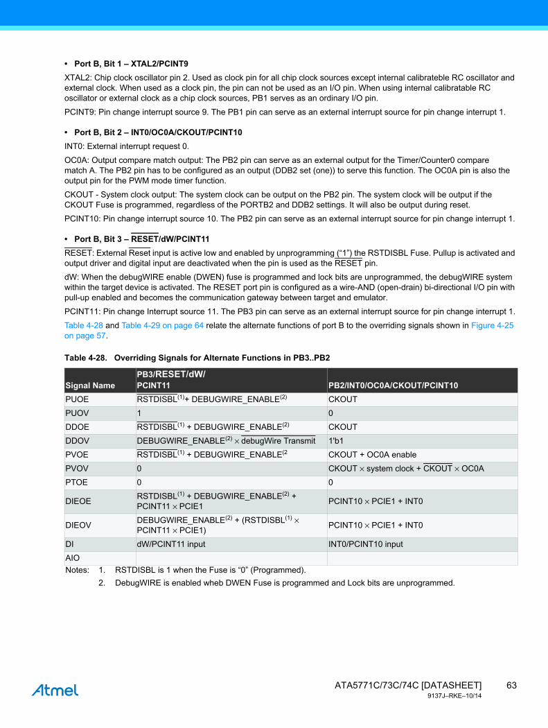
• Port B, Bit 1 – XTAL2/PCINT9
XTAL2: Chip clock oscillator pin 2. Used as clock pin for all chip clock sources except internal calibrateble RC oscillator and external clock. When used as a clock pin, the pin can not be used as an I/O pin. When using internal calibratable RC oscillator or external clock as a chip clock sources, PB1 serves as an ordinary I/O pin.
PCINT9: Pin change interrupt source 9. The PB1 pin can serve as an external interrupt source for pin change interrupt 1.
• Port B, Bit 2 – INT0/OC0A/CKOUT/PCINT10
INT0: External interrupt request 0.
OC0A: Output compare match output: The PB2 pin can serve as an external output for the Timer/Counter0 compare match A. The PB2 pin has to be configured as an output (DDB2 set (one)) to serve this function. The OC0A pin is also the output pin for the PWM mode timer function.
CKOUT - System clock output: The system clock can be output on the PB2 pin. The system clock will be output if the CKOUT Fuse is programmed, regardless of the PORTB2 and DDB2 settings. It will also be output during reset.
PCINT10: Pin change interrupt source 10. The PB2 pin can serve as an external interrupt source for pin change interrupt 1.
• Port B, Bit 3 – RESET/dW/PCINT11
RESET: External Reset input is active low and enabled by unprogramming (“1”) the RSTDISBL Fuse. Pullup is activated and output driver and digital input are deactivated when the pin is used as the RESET pin.
dW: When the debugWIRE enable (DWEN) fuse is programmed and lock bits are unprogrammed, the debugWIRE system within the target device is activated. The RESET port pin is configured as a wire-AND (open-drain) bi-directional I/O pin with pull-up enabled and becomes the communication gateway between target and emulator.
PCINT11: Pin change Interrupt source 11. The PB3 pin can serve as an external interrupt source for pin change interrupt 1.
Table 4-28 and Table 4-29 on page 64 relate the alternate functions of port B to the overriding signals shown in Figure 4-25 on page 57.
Table 4-28. Overriding Signals for Alternate Functions in PB3..PB2
Signal NamePB3/RESET/dW/PCINT11 PB2/INT0/OC0A/CKOUT/PCINT10
PUOE RSTDISBL(1)+ DEBUGWIRE_ENABLE(2) CKOUT
PUOV 1 0
DDOE RSTDISBL(1) + DEBUGWIRE_ENABLE(2) CKOUT
DDOV DEBUGWIRE_ENABLE(2) × debugWire Transmit 1'b1
PVOE RSTDISBL(1) + DEBUGWIRE_ENABLE(2 CKOUT + OC0A enable
PVOV 0 CKOUT × system clock + CKOUT × OC0A
PTOE 0 0
DIEOERSTDISBL(1) + DEBUGWIRE_ENABLE(2) + PCINT11 × PCIE1
PCINT10 × PCIE1 + INT0
DIEOVDEBUGWIRE_ENABLE(2) + (RSTDISBL(1) × PCINT11 × PCIE1)
PCINT10 × PCIE1 + INT0
DI dW/PCINT11 input INT0/PCINT10 input
AIO
Notes: 1. RSTDISBL is 1 when the Fuse is “0” (Programmed).
2. DebugWIRE is enabled wheb DWEN Fuse is programmed and Lock bits are unprogrammed.
63ATA5771C/73C/74C [DATASHEET]9137J–RKE–10/14

4.14.4 Register Description
4.14.4.1 MCUCR – MCU Control Register
• Bit 6 – PUD: Pull-up Disable
When this bit is written to one, the pull-ups in the I/O ports are disabled even if the DDxn and PORTxn registers are configured to enable the pull-ups ({DDxn, PORTxn} = 0b01). See Section 4.14.2.1 “Configuring the Pin” on page 53 for more details about this feature.
4.14.4.2 PORTA – Port A Data Register
4.14.4.3 DDRA – Port A Data Direction Register
Table 4-29. Overriding Signals for Alternate Functions in PB1..PB0
Signal Name PB1/XTAL2/PCINT9 PB0/XTAL1/PCINT8
PUOE EXT_OSC(1) EXT_CLOCK(2)+ EXT_OSC(1)
PUOV 0 0
DDOE EXT_OSC(1) EXT_CLOCK(2) + EXT_OSC(1)
DDOV 0 0
PVOE EXT_OSC(1) EXT_CLOCK(2) + EXT_OSC(1)
PVOV 0 0
PTOE 0 0
DIEOE EXT_OSC(1)+ PCINT9 × PCIE1 EXT_CLOCK(2) + EXT_OSC(1) + (PCINT8 × PCIE1)
DIEOV EXT_OSC(1) × PCINT9 × PCIE1(EXT_CLOCK(2) × PWR_DOWN) +
(EXT_CLOCK(2) × EXT_OSC(1) × PCINT8 × PCIE1)
DI PCINT9 input CLOCK/PCINT8 input
AIO XTAL2 XTAL1
Notes: 1. EXT_OSC = crystal oscillator or low frequency crystal oscillator is selected as system clock.
2. EXT_CLOCK = external clock is selected as system clock.
Bit 7 6 5 4 3 2 1 0
BODS PUD SE SM1 SM0 BODSE ISC01 ISC00 MCUCR
Read/Write R/W R/W R/W R/W R/W R/W R/W R/W
Initial Value 0 0 0 0 0 0 0 0
Bit 7 6 5 4 3 2 1 0
0x1B (0x3B) PORTA7 PORTA6 PORTA5 PORTA4 PORTA3 PORTA2 PORTA1 PORTA0 PORTA
Read/Write R/W R/W R/W R/W R/W R/W R/W R/W
Initial Value 0 0 0 0 0 0 0 0
Bit 7 6 5 4 3 2 1 0
0x1A (0x3A) DDA7 DDA6 DDA5 DDA4 DDA3 DDA2 DDA1 DDA0 DDRB
Read/Write R/W R/W R/W R/W R/W R/W R/W R/W
Initial Value 0 0 0 0 0 0 0 0
ATA5771C/73C/74C [DATASHEET]9137J–RKE–10/14
64

4.14.4.4 PINA – Port A Input Pins Address
4.14.4.5 PORTB – Port B Data Register
4.14.4.6 DDRB – Port B Data Direction Register
4.14.4.7 PINB – Port BInput Pins Address
Bit 7 6 5 4 3 2 1 0
0x19 (0x39) PINA7 PINA6 PINA5 PINA4 PINA3 PINA2 PINA1 PINA0 PINB
Read/Write R/W R/W R/W R/W R/W R/W R/W R/W
Initial Value 0 0 N/A N/A N/A N/A N/A N/A
Bit 7 6 5 4 3 2 1 0
0x18 (0x38) – – PORTB3 PORTB2 PORTB1 PORTB0 PORTB
Read/Write R R R R R/W R/W R/W R/W
Initial Value 0 0 0 0 0 0 0 0
Bit 7 6 5 4 3 2 1 0
0x17 (0x37) – – DDB3 DDB2 DDB1 DDB0 DDRB
Read/Write R R R R R/W R/W R/W R/W
Initial Value 0 0 0 0 0 0 0 0
Bit 7 6 5 4 3 2 1 0
0x16 (0x36) – – PINB3 PINB2 PINB1 PINB0 PINB
Read/Write R R R R R/W R/W R/W R/W
Initial Value 0 0 N/A N/A N/A N/A N/A N/A
65ATA5771C/73C/74C [DATASHEET]9137J–RKE–10/14

4.15 8-bit Timer/Counter0 with PWM
4.15.1 Features
● Two independent output compare units
● Double buffered output compare registers
● Clear timer on compare match (auto reload)
● Glitch free, phase correct pulse width modulator (PWM)
● Variable PWM period
● Frequency generator
● Three independent interrupt sources (TOV0, OCF0A, and OCF0B)
4.15.2 Overview
Timer/Counter0 is a general purpose 8-bit Timer/Counter module, with two independent output compare units, and with PWM support. It allows accurate program execution timing (event management) and wave generation.
A simplified block diagram of the 8-bit Timer/Counter is shown in Figure 4-26. For the actual placement of I/O pins. CPU accessible I/O registers, including I/O bits and I/O pins, are shown in bold. The device-specific I/O register and bit locations are listed in the Section 4.9.10 “Register Description” on page 33.
Figure 4-26. 8-bit Timer/Counter Block Diagram
TCNTn
Timer/Counter
CountClear
Direction
OCRnA
OCRnB
TCCRnA TCCRnB
=
TOP BOTTOM
OCnA (Int. Req.)
WaveformGeneration
FixedTOPValue
DAT
A B
US
=
= = 0
OCnA
OCnB (Int. Req.)
WaveformGeneration OCnB
Control Logic clkTn
TOVn (Int. Req.)
EdgeDetector
(From Prescaler)
Clock Select
Tn
ATA5771C/73C/74C [DATASHEET]9137J–RKE–10/14
66

4.15.2.1 Registers
The Timer/Counter (TCNT0) and output compare registers (OCR0A and OCR0B) are 8-bit registers. Interrupt request (abbreviated to int.req. in the figure) signals are all visible in the timer interrupt flag register (TIFR0). All interrupts are individually masked with the timer interrupt mask register (TIMSK0). TIFR0 and TIMSK0 are not shown in the figure.
The Timer/Counter can be clocked internally, via the prescaler, or by an external clock source on the T0 pin. The clock select logic block controls which clock source and edge the Timer/Counter uses to increment (or decrement) its value. The Timer/Counter is inactive when no clock source is selected. The output from the clock select logic is referred to as the timer clock (clkT0).
The double buffered output compare registers (OCR0A and OCR0B) is compared with the Timer/Counter value at all times. The result of the compare can be used by the waveform generator to generate a PWM or variable frequency output on the output compare pins (OC0A and OC0B). See Section 4.15.5 “Output Compare Unit” on page 68 for details. The compare match event will also set the compare flag (OCF0A or OCF0B) which can be used to generate an output compare interrupt request.
4.15.2.2 Definitions
Many register and bit references in this section are written in general form. A lower case “n” replaces the Timer/Counter number, in this case 0. A lower case “x” replaces the output compare unit, in this case compare unit A or compare unit B. However, when using the register or bit defines in a program, the precise form must be used, i.e., TCNT0 for accessing Timer/Counter0 counter value and so on.
The definitions in Table 4-30 are also used extensively throughout the document.
4.15.3 Timer/Counter Clock Sources
The Timer/Counter can be clocked by an internal or an external clock source. The clock source is selected by the clock select logic which is controlled by the clock select (CS02:0) bits located in the Timer/Counter Control Register (TCCR0B). For details on clock sources and prescaler, see Section 4.17 “Timer/Counter Prescaler” on page 105.
4.15.4 Counter Unit
The main part of the 8-bit Timer/Counter is the programmable bi-directional counter unit. Table 4-27 shows a block diagram of the counter and its surroundings.
Figure 4-27. Counter Unit Block Diagram
Table 4-30. Definitions
Definitions
BOTTOM The counter reaches the BOTTOM when it becomes 0x00.MAX The counter reaches its MAXimum when it becomes 0xFF (decimal 255).TOP The counter reaches the TOP when it becomes equal to the highest value in the count sequence. The TOP
value can be assigned to be the fixed value 0xFF (MAX) or the value stored in the OCR0A register. The assignment is dependent on the mode of operation.
TopBottom
TOVn(Int. Req.)DATA BUS
Control LogicTCNTnclkTn
Count
Clear
Direction
EdgeDetector
(From Prescaler)
Clock Select
Tn
67ATA5771C/73C/74C [DATASHEET]9137J–RKE–10/14

Signal description (internal signals):
count Increment or decrement TCNT0 by 1.
direction Select between increment and decrement.
clear Clear TCNT0 (set all bits to zero).
clkTn Timer/Counter clock, referred to as clkT0 in the following.
top Signalize that TCNT0 has reached maximum value.
bottom Signalize that TCNT0 has reached minimum value (zero).
Depending of the mode of operation used, the counter is cleared, incremented, or decremented at each timer clock (clkT0). clkT0 can be generated from an external or internal clock source, selected by the Clock Select bits (CS02:0). When no clock source is selected (CS02:0 = 0) the timer is stopped. However, the TCNT0 value can be accessed by the CPU, regardless of whether clkT0 is present or not. A CPU write overrides (has priority over) all counter clear or count operations.
The counting sequence is determined by the setting of the WGM01 and WGM00 bits located in the Timer/Counter Control Register (TCCR0A) and the WGM02 bit located in the Timer/Counter Control Register B (TCCR0B). There are close connections between how the counter behaves (counts) and how waveforms are generated on the output compare output OC0A. For more details about advanced counting sequences and waveform generation, see Section 4.15.7 “Modes of Operation” on page 70.
The Timer/Counter Overflow Flag (TOV0) is set according to the mode of operation selected by the WGM01:0 bits. TOV0 can be used for generating a CPU interrupt.
4.15.5 Output Compare Unit
The 8-bit comparator continuously compares TCNT0 with the output compare registers (OCR0A and OCR0B). Whenever TCNT0 equals OCR0A or OCR0B, the comparator signals a match. A match will set the output compare flag (OCF0A or OCF0B) at the next timer clock cycle. If the corresponding interrupt is enabled, the output compare flag generates an output compare interrupt. The output compare flag is automatically cleared when the interrupt is executed. Alternatively, the flag can be cleared by software by writing a logical one to its I/O bit location. The waveform generator uses the match signal to generate an output according to operating mode set by the WGM02:0 bits and compare output mode (COM0x1:0) bits. The max and bottom signals are used by the waveform generator for handling the special cases of the extreme values in some modes of operation. See Section 4.15.7 “Modes of Operation” on page 70.
Figure 4-28 shows a block diagram of the output compare unit.
Figure 4-28. Output Compare Unit, Block Diagram
OCFnx (Int. Req.)
= (8-bit Comparator)
OCRnx
Waveform Generator
TCNTn
OCnx
Top
Bottom
FOCn
WGMn1:0 COMnX1:0
DATA BUS
ATA5771C/73C/74C [DATASHEET]9137J–RKE–10/14
68

The OCR0x registers are double buffered when using any of the pulse width modulation (PWM) modes. For the normal and clear timer on compare (CTC) modes of operation, the double buffering is disabled. The double buffering synchronizes the update of the OCR0x compare registers to either top or bottom of the counting sequence. The synchronization prevents the occurrence of odd-length, non-symmetrical PWM pulses, thereby making the output glitch-free.
The OCR0x register access may seem complex, but this is not case. When the double buffering is enabled, the CPU has access to the OCR0x buffer register, and if double buffering is disabled the CPU will access the OCR0x directly.
4.15.5.1 Force Output Compare
In non-PWM waveform generation modes, the match output of the comparator can be forced by writing a one to the force output compare (0x) bit. Forcing compare match will not set the OCF0x flag or reload/clear the timer, but the OC0x pin will be updated as if a real compare match had occurred (the COM0x1:0 bits settings define whether the OC0x pin is set, cleared or toggled).
4.15.5.2 Compare Match Blocking by TCNT0 Write
All CPU write operations to the TCNT0 register will block any compare match that occur in the next timer clock cycle, even when the timer is stopped. This feature allows OCR0x to be initialized to the same value as TCNT0 without triggering an interrupt when the Timer/Counter clock is enabled.
4.15.5.3 Using the Output Compare Unit
Since writing TCNT0 in any mode of operation will block all compare matches for one timer clock cycle, there are risks involved when changing TCNT0 when using the output compare unit, independently of whether the Timer/Counter is running or not. If the value written to TCNT0 equals the OCR0x value, the compare match will be missed, resulting in incorrect waveform generation. Similarly, do not write the TCNT0 value equal to BOTTOM when the counter is down-counting.
The setup of the OC0x should be performed before setting the data direction register for the port pin to output. The easiest way of setting the OC0x value is to use the force output compare (0x) strobe bits in normal mode. The OC0x registers keep their values even when changing between waveform generation modes.
Be aware that the COM0x1:0 bits are not double buffered together with the compare value. Changing the COM0x1:0 bits will take effect immediately.
4.15.6 Compare Match Output Unit
The compare output mode (COM0x1:0) bits have two functions. The waveform generator uses the COM0x1:0 bits for defining the output compare (OC0x) state at the next compare match. Also, the COM0x1:0 bits control the OC0x pin output source. Figure 4-29 on page 70 shows a simplified schematic of the logic affected by the COM0x1:0 bit setting. The I/O registers, I/O bits, and I/O pins in the figure are shown in bold. Only the parts of the general I/O port control registers (DDR and PORT) that are affected by the COM0x1:0 bits are shown. When referring to the OC0x state, the reference is for the internal OC0x register, not the OC0x pin. If a system reset occur, the OC0x register is reset to “0”.
69ATA5771C/73C/74C [DATASHEET]9137J–RKE–10/14

Figure 4-29. Compare Match Output Unit, Schematic
The general I/O port function is overridden by the output compare (OC0x) from the waveform generator if either of the COM0x1:0 bits are set. However, the OC0x pin direction (input or output) is still controlled by the data direction register (DDR) for the port pin. The data direction register bit for the OC0x pin (DDR_OC0x) must be set as output before the OC0x value is visible on the pin. The port override function is independent of the waveform generation mode.
The design of the output compare pin logic allows initialization of the OC0x state before the output is enabled. Note that some COM0x1:0 bit settings are reserved for certain modes of operation, see Section 4.10.9 “Register Description” on page 37
4.15.6.1 Compare Output Mode and Waveform Generation
The waveform generator uses the COM0x1:0 bits differently in normal, CTC, and PWM modes. For all modes, setting the COM0x1:0 = 0 tells the waveform generator that no action on the OC0x Register is to be performed on the next compare match. For compare output actions in the non-PWM modes refer to Table 4-31 on page 76. For fast PWM mode, refer to Table 4-32 on page 76, and for phase correct PWM refer to Table 4-33 on page 76.
A change of the COM0x1:0 bits state will have effect at the first compare match after the bits are written. For non-PWM modes, the action can be forced to have immediate effect by using the 0x strobe bits.
4.15.7 Modes of Operation
The mode of operation, i.e., the behavior of the Timer/Counter and the output compare pins, is defined by the combination of the waveform generation mode (WGM02:0) and compare output mode (COM0x1:0) bits. The compare output mode bits do not affect the counting sequence, while the waveform generation mode bits do. The COM0x1:0 bits control whether the PWM output generated should be inverted or not (inverted or non-inverted PWM). For non-PWM modes the COM0x1:0 bits control whether the output should be set, cleared, or toggled at a compare match (See Section 4.15.7 “Modes of Operation” on page 70).
For detailed timing information refer to Figure 4-33 on page 74, Figure 4-34 on page 74, Figure 4-35 on page 75 and Figure 4-36 on page 75 in Section 4.15.8 “Timer/Counter Timing Diagrams” on page 74.
DAT
A B
US
0
1
QD
COMnx1
COMnx0
FOCn
OCnx
WaveformGenerator
QD
PORT
QD
DDR
OCnxPin
clkI/O
ATA5771C/73C/74C [DATASHEET]9137J–RKE–10/14
70

4.15.7.1 Normal Mode
The simplest mode of operation is the Normal mode (WGM02:0 = 0). In this mode the counting direction is always up (incrementing), and no counter clear is performed. The counter simply overruns when it passes its maximum 8-bit value (TOP = 0xFF) and then restarts from the bottom (0x00). In normal operation the Timer/Counter Overflow Flag (TOV0) will be set in the same timer clock cycle as the TCNT0 becomes zero. The TOV0 Flag in this case behaves like a ninth bit, except that it is only set, not cleared. However, combined with the timer overflow interrupt that automatically clears the TOV0 Flag, the timer resolution can be increased by software. There are no special cases to consider in the normal mode, a new counter value can be written anytime.
The output compare Unit can be used to generate interrupts at some given time. Using the output compare to generate waveforms in normal mode is not recommended, since this will occupy too much of the CPU time.
4.15.7.2 Clear Timer on Compare Match (CTC) Mode
In clear timer on compare or CTC mode (WGM02:0 = 2), the OCR0A register is used to manipulate the counter resolution. In CTC mode the counter is cleared to zero when the counter value (TCNT0) matches the OCR0A. The OCR0A defines the top value for the counter, hence also its resolution. This mode allows greater control of the compare match output frequency. It also simplifies the operation of counting external events.
The timing diagram for the CTC mode is shown in Figure 4-30. The counter value (TCNT0) increases until a compare match occurs between TCNT0 and OCR0A, and then counter (TCNT0) is cleared.
Figure 4-30. CTC Mode, Timing Diagram
An interrupt can be generated each time the counter value reaches the TOP value by using the OCF0A Flag. If the interrupt is enabled, the interrupt handler routine can be used for updating the TOP value. However, changing TOP to a value close to BOTTOM when the counter is running with none or a low prescaler value must be done with care since the CTC mode does not have the double buffering feature. If the new value written to OCR0A is lower than the current value of TCNT0, the counter will miss the compare match. The counter will then have to count to its maximum value (0xFF) and wrap around starting at 0x00 before the compare match can occur.
For generating a waveform output in CTC mode, the OC0A output can be set to toggle its logical level on each compare match by setting the compare output mode bits to toggle mode (COM0A1:0 = 1). The OC0A value will not be visible on the port pin unless the data direction for the pin is set to output. The waveform generated will have a maximum frequency of
0 = fclk_I/O/2 when OCR0A is set to zero (0x00). The waveform frequency is defined by the following equation:
The N variable represents the prescale factor (1, 8, 64, 256, or 1024).
As for the normal mode of operation, the TOV0 Flag is set in the same timer clock cycle that the counter counts from MAX to 0x00.
1 2
TCNTn
(COMnx1:0 = 1)OCnx(Toggle)
Period3
OCnx InterruptFlag Set
4
fOCnxfclk_I/O
2 N 1 OCRnx+( )⋅ ⋅-------------------------------------------------=
71ATA5771C/73C/74C [DATASHEET]9137J–RKE–10/14

4.15.7.3 Fast PWM Mode
The fast pulse width modulation or fast PWM mode (WGM02:0 = 3 or 7) provides a high frequency PWM waveform generation option. The fast PWM differs from the other PWM option by its single-slope operation. The counter counts from BOTTOM to TOP then restarts from BOTTOM. TOP is defined as 0xFF when WGM2:0 = 3, and OCR0A when WGM2:0 = 7. In non-inverting compare output mode, the output compare (OC0x) is cleared on the compare match between TCNT0 and OCR0x, and set at BOTTOM. In inverting Compare Output mode, the output is set on Compare Match and cleared at BOTTOM. Due to the single-slope operation, the operating frequency of the fast PWM mode can be twice as high as the phase correct PWM mode that use dual-slope operation. This high frequency makes the fast PWM mode well suited for power regulation, rectification, and DAC applications. High frequency allows physically small sized external components (coils, capacitors), and therefore reduces total system cost.
In fast PWM mode, the counter is incremented until the counter value matches the TOP value. The counter is then cleared at the following timer clock cycle. The timing diagram for the fast PWM mode is shown in Figure 4-31. The TCNT0 value is in the timing diagram shown as a histogram for illustrating the single-slope operation. The diagram includes non-inverted and inverted PWM outputs. The small horizontal line marks on the TCNT0 slopes represent compare matches between OCR0x and TCNT0.
Figure 4-31. Fast PWM Mode, Timing Diagram
The Timer/Counter Overflow Flag (TOV0) is set each time the counter reaches TOP. If the interrupt is enabled, the interrupt handler routine can be used for updating the compare value.
In fast PWM mode, the compare unit allows generation of PWM waveforms on the OC0x pins. Setting the COM0x1:0 bits to two will produce a non-inverted PWM and an inverted PWM output can be generated by setting the COM0x1:0 to three: Setting the COM0A1:0 bits to one allows the AC0A pin to toggle on compare matches if the WGM02 bit is set. This option is not available for the OC0B pin (See Table 4-32 on page 76). The actual OC0x value will only be visible on the port pin if the data direction for the port pin is set as output. The PWM waveform is generated by setting (or clearing) the OC0x register at the compare match between OCR0x and TCNT0, and clearing (or setting) the OC0x register at the timer clock cycle the counter is cleared (changes from TOP to BOTTOM).
The PWM frequency for the output can be calculated by the following equation:
The N variable represents the prescale factor (1, 8, 64, 256, or 1024).
The extreme values for the OCR0A register represents special cases when generating a PWM waveform output in the fast PWM mode. If the OCR0A is set equal to BOTTOM, the output will be a narrow spike for each MAX+1 timer clock cycle. Setting the OCR0A equal to MAX will result in a constantly high or low output (depending on the polarity of the output set by the COM0A1:0 bits.)
1 2 3 4 5 6 7
TCNTn
(COMnx1:0 = 2)
(COMnx1:0 = 3)
OCn
OCn
Period
OCRnx Update andTOVn Interrupt Flag Set
OCRnx InterruptFlag Set
fOCnxPWMfclk_I/ON 256⋅-----------------=
ATA5771C/73C/74C [DATASHEET]9137J–RKE–10/14
72

A frequency (with 50% duty cycle) waveform output in fast PWM mode can be achieved by setting OC0x to toggle its logical level on each compare match (COM0x1:0 = 1). The waveform generated will have a maximum frequency of 0 = fclk_I/O/2 when OCR0A is set to zero. This feature is similar to the OC0A toggle in CTC mode, except the double buffer feature of the output compare unit is enabled in the fast PWM mode.
4.15.7.4 Phase Correct PWM Mode
The phase correct PWM mode (WGM02:0 = 1 or 5) provides a high resolution phase correct PWM waveform generation option. The phase correct PWM mode is based on a dual-slope operation. The counter counts repeatedly from BOTTOM to TOP and then from TOP to BOTTOM. TOP is defined as 0xFF when WGM2:0 = 1, and OCR0A when WGM2:0 = 5. In non-inverting compare output mode, the output compare (OC0x) is cleared on the compare match between TCNT0 and OCR0x while upcounting, and set on the compare match while down-counting. In inverting output compare mode, the operation is inverted. The dual-slope operation has lower maximum operation frequency than single slope operation. However, due to the symmetric feature of the dual-slope PWM modes, these modes are preferred for motor control applications.
In phase correct PWM mode the counter is incremented until the counter value matches TOP. When the counter reaches TOP, it changes the count direction. The TCNT0 value will be equal to TOP for one timer clock cycle. The timing diagram for the phase correct PWM mode is shown on Figure 4-32 on page 73. The TCNT0 value is in the timing diagram shown as a histogram for illustrating the dual-slope operation. The diagram includes non-inverted and inverted PWM outputs. The small horizontal line marks on the TCNT0 slopes represent compare matches between OCR0x and TCNT0.
Figure 4-32. Phase Correct PWM Mode, Timing Diagram
The Timer/Counter Overflow Flag (TOV0) is set each time the counter reaches BOTTOM. The interrupt flag can be used to generate an interrupt each time the counter reaches the BOTTOM value.
In phase correct PWM mode, the compare unit allows generation of PWM waveforms on the OC0x pins. Setting the COM0x1:0 bits to two will produce a non-inverted PWM. An inverted PWM output can be generated by setting the COM0x1:0 to three: Setting the COM0A0 bits to one allows the OC0A pin to toggle on compare matches if the WGM02 bit is set. This option is not available for the OC0B pin (See Table 4-33 on page 76). The actual OC0x value will only be visible on the port pin if the data direction for the port pin is set as output.
The PWM waveform is generated by clearing (or setting) the OC0x register at the compare match between OCR0x and TCNT0 when the counter increments, and setting (or clearing) the OC0x register at compare match between OCR0x and TCNT0 when the counter decrements. The PWM frequency for the output when using phase correct PWM can be calculated by the following equation:
1 2 3
TCNTn
(COMnx1:0 = 2)
(COMnx1:0 = 3)
OCn
OCn
Period
TOVn InterruptFlag Set
OCRnx Update
OCnx InterruptFlag Set
fOCnxPCPWMfclk_I/ON 510⋅-----------------=
73ATA5771C/73C/74C [DATASHEET]9137J–RKE–10/14
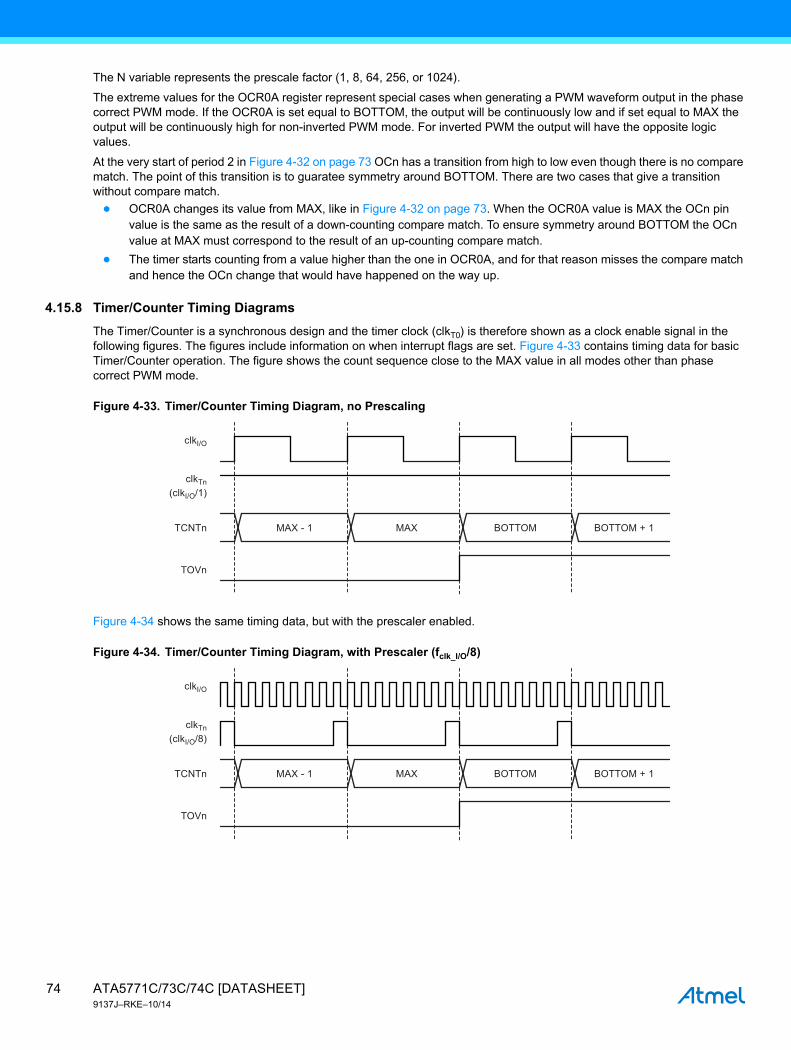
The N variable represents the prescale factor (1, 8, 64, 256, or 1024).
The extreme values for the OCR0A register represent special cases when generating a PWM waveform output in the phase correct PWM mode. If the OCR0A is set equal to BOTTOM, the output will be continuously low and if set equal to MAX the output will be continuously high for non-inverted PWM mode. For inverted PWM the output will have the opposite logic values.
At the very start of period 2 in Figure 4-32 on page 73 OCn has a transition from high to low even though there is no compare match. The point of this transition is to guaratee symmetry around BOTTOM. There are two cases that give a transition without compare match.
● OCR0A changes its value from MAX, like in Figure 4-32 on page 73. When the OCR0A value is MAX the OCn pin value is the same as the result of a down-counting compare match. To ensure symmetry around BOTTOM the OCn value at MAX must correspond to the result of an up-counting compare match.
● The timer starts counting from a value higher than the one in OCR0A, and for that reason misses the compare match and hence the OCn change that would have happened on the way up.
4.15.8 Timer/Counter Timing Diagrams
The Timer/Counter is a synchronous design and the timer clock (clkT0) is therefore shown as a clock enable signal in the following figures. The figures include information on when interrupt flags are set. Figure 4-33 contains timing data for basic Timer/Counter operation. The figure shows the count sequence close to the MAX value in all modes other than phase correct PWM mode.
Figure 4-33. Timer/Counter Timing Diagram, no Prescaling
Figure 4-34 shows the same timing data, but with the prescaler enabled.
Figure 4-34. Timer/Counter Timing Diagram, with Prescaler (fclk_I/O/8)
MAX - 1
clkI/O
(clkI/O/1)
TCNTn
TOVn
clkTn
MAX BOTTOM BOTTOM + 1
MAX - 1
clkI/O
(clkI/O/8)
TCNTn
TOVn
clkTn
MAX BOTTOM BOTTOM + 1
ATA5771C/73C/74C [DATASHEET]9137J–RKE–10/14
74
Figure 4-35 shows the setting of OCF0B in all modes and OCF0A in all modes except CTC mode and PWM mode, where OCR0A is TOP.
Figure 4-35. Timer/Counter Timing Diagram, Setting of OCF0x, with Prescaler (fclk_I/O/8)
Figure 4-36 shows the setting of OCF0A and the clearing of TCNT0 in CTC mode and fast PWM mode where OCR0A is TOP.
Figure 4-36. Timer/Counter Timing Diagram, Clear Timer on Compare Match mode, with Prescaler (fclk_I/O/8)
4.15.9 Register Description
4.15.9.1 TCCR0A – Timer/Counter Control Register A
• Bits 7:6 – COM0A1:0: Compare Match Output A Mode
These bits control the output compare pin (OC0A) behavior. If one or both of the COM0A1:0 bits are set, the OC0A output overrides the normal port functionality of the I/O pin it is connected to. However, note that the data direction register (DDR) bit corresponding to the OC0A pin must be set in order to enable the output driver.
When OC0A is connected to the pin, the function of the COM0A1:0 bits depends on the WGM02:0 bit setting. Table 4-31 shows the COM0A1:0 bit functionality when the WGM02:0 bits are set to a normal or CTC mode (non-PWM).
OCRnx - 1
clkI/O
(clkI/O/8)
TCNTn
OCRnx
OCFnx
clkTn
OCRnx OCRnx + 1
OCRnx Value
OCRnx + 2
TOP - 1
clkI/O
(clkI/O/8)
TCNTn(CTC)
OCRnx
OCFnx
clkTn
TOP BOTTOM
TOP
BOTTOM + 1
Bit 7 6 5 4 3 2 1 0
0x30 (0x50) COM0A1 COM0A0 COM0B1 COM0B0 – – WGM01 WGM00 TCCR0A
Read/Write R/W R/W R/W R/W R R R/W R/W
Initial Value 0 0 0 0 0 0 0 0
75ATA5771C/73C/74C [DATASHEET]9137J–RKE–10/14
Table 4-32 shows the COM0A1:0 bit functionality when the WGM01:0 bits are set to fast PWM mode.
Table 4-33 shows the COM0A1:0 bit functionality when the WGM02:0 bits are set to phase correct PWM mode.
• Bits 5:4 – COM0B1:0: Compare Match Output B Mode
These bits control the output compare pin (OC0B) behavior. If one or both of the COM0B1:0 bits are set, the OC0B output overrides the normal port functionality of the I/O pin it is connected to. However, note that the data direction register (DDR) bit corresponding to the OC0B pin must be set in order to enable the output driver.
When OC0B is connected to the pin, the function of the COM0B1:0 bits depends on the WGM02:0 bit setting. Table 4-34 shows the COM0A1:0 bit functionality when the WGM02:0 bits are set to a normal or CTC mode (non-PWM).
Table 4-31. Compare Output Mode, non-PWM Mode
COM01 COM00 Description
0 0 Normal port operation, OC0A disconnected.
0 1 Toggle OC0A on compare match
1 0 Clear OC0A on compare match
1 1 Set OC0A on compare match
Table 4-32. Compare Output Mode, Fast PWM Mode(1)
COM01 COM00 Description
0 0 Normal port operation, OC0A disconnected.
0 1WGM02 = 0: Normal port operation, OC0A disconnected.WGM02 = 1: Toggle OC0A on compare match.
1 0 Clear OC0A on compare match, set OC0A at BOTTOM (non-inverting mode)
1 1 Set OC0A on compare match, clear OC0A at BOTTOM (inverting mode)
Note: 1. A special case occurs when OCR0A equals TOP and COM0A1 is set. In this case, the compare match is ignored, but the set or clear is done at BOTTOM. See Section 4.15.7.3 “Fast PWM Mode” on page 72 for more details.
Table 4-33. Compare Output Mode, Phase Correct PWM Mode(1)
COM0A1 COM0A0 Description
0 0 Normal port operation, OC0A disconnected.
0 1WGM02 = 0: Normal port operation, OC0A disconnected.WGM02 = 1: Toggle OC0A on compare match.
1 0Clear OC0A on compare match when up-counting. Set OC0A on compare match when down-counting.
1 1Set OC0A on compare match when up-counting. Clear OC0A on compare match when down-counting.
Note: 1. A special case occurs when OCR0A equals TOP and COM0A1 is set. In this case, the compare match is ignored, but the set or clear is done at TOP. See Section 4.15.7.4 “Phase Correct PWM Mode” on page 73 for more details.
Table 4-34. Compare Output Mode, non-PWM Mode
COM01 COM00 Description
0 0 Normal port operation, OC0B disconnected.
0 1 Toggle OC0B on compare match
1 0 Clear OC0B on compare match
1 1 Set OC0B on compare match
ATA5771C/73C/74C [DATASHEET]9137J–RKE–10/14
76

Table 4-35 shows the COM0B1:0 bit functionality when the WGM02:0 bits are set to fast PWM mode.
Table 4-36 shows the COM0B1:0 bit functionality when the WGM02:0 bits are set to phase correct PWM mode.
• Bits 3, 2 – Res: Reserved Bits
These bits are reserved bits in the ATtiny44V and will always read as zero.
• Bits 1:0 – WGM01:0: Waveform Generation Mode
Combined with the WGM02 bit found in the TCCR0B register, these bits control the counting sequence of the counter, the source for maximum (TOP) counter value, and what type of waveform generation to be used, see Table 4-37. Modes of operation supported by the Timer/Counter unit are: Normal mode (counter), clear timer on compare match (CTC) mode, and two types of pulse width modulation (PWM) modes (see Section 4.15.7 “Modes of Operation” on page 70).
Table 4-35. Compare Output Mode, Fast PWM Mode(1)
COM01 COM00 Description
0 0 Normal port operation, OC0B disconnected.
0 1 Reserved
1 0Clear OC0B on compare match, set OC0B at BOTTOM(non-inverting mode)
1 1Set OC0B on compare match, clear OC0B at BOTTOM(inverting mode)
Note: 1. A special case occurs when OCR0B equals TOP and COM0B1 is set. In this case, the compare match is ignored, but the set or clear is done at BOTTOM. See Section 4.15.7.3 “Fast PWM Mode” on page 72 for more details.
Table 4-36. Compare Output Mode, Phase Correct PWM Mode(1)
COM0A1 COM0A0 Description
0 0 Normal port operation, OC0B disconnected.
0 1 Reserved
1 0Clear OC0B on compare match when up-counting. Set OC0B on compare match when down-counting.
1 1Set OC0B on compare match when up-counting. Clear OC0B on compare match when down-counting.
Note: 1. A special case occurs when OCR0B equals TOP and COM0B1 is set. In this case, the compare match is ignored, but the set or clear is done at TOP. See Section 4.15.7.4 “Phase Correct PWM Mode” on page 73 for more details.
Table 4-37. Waveform Generation Mode Bit Description
Mode WGM2 WGM1 WGM0Timer/Counter Mode of Operation TOP
Update ofOCRx at
TOV FlagSet on(1)
0 0 0 0 Normal 0xFF Immediate MAX
1 0 0 1 PWM, phase correct 0xFF TOP BOTTOM
2 0 1 0 CTC OCRA Immediate MAX
3 0 1 1 Fast PWM 0xFF BOTTOM MAX
4 1 0 0 Reserved – – –
5 1 0 1 PWM, phase correct OCRA TOP BOTTOM
6 1 1 0 Reserved – – –
7 1 1 1 Fast PWM OCRA BOTTOM TOP
Note: 1. MAX = 0xFFBOTTOM = 0x00
77ATA5771C/73C/74C [DATASHEET]9137J–RKE–10/14

4.15.9.2 TCCR0B – Timer/Counter Control Register B
• Bit 7 – FOC0A: Force Output Compare A
The FOC0A bit is only active when the WGM bits specify a non-PWM mode.
However, for ensuring compatibility with future devices, this bit must be set to zero when TCCR0B is written when operating in PWM mode. When writing a logical one to the FOC0A bit, an immediate compare match is forced on the waveform generation unit. The OC0A output is changed according to its COM0A1:0 bits setting. Note that the FOC0A bit is implemented as a strobe. Therefore it is the value present in the COM0A1:0 bits that determines the effect of the forced compare.
A FOC0A strobe will not generate any interrupt, nor will it clear the timer in CTC mode using OCR0A as TOP.
The FOC0A bit is always read as zero.
• Bit 6 – FOC0B: Force Output Compare B
The FOC0B bit is only active when the WGM bits specify a non-PWM mode.
However, for ensuring compatibility with future devices, this bit must be set to zero when TCCR0B is written when operating in PWM mode. When writing a logical one to the FOC0B bit, an immediate compare match is forced on the waveform generation unit. The OC0B output is changed according to its COM0B1:0 bits setting. Note that the FOC0B bit is implemented as a strobe. Therefore it is the value present in the COM0B1:0 bits that determines the effect of the forced compare.
A FOC0B strobe will not generate any interrupt, nor will it clear the timer in CTC mode using OCR0B as TOP.
The FOC0B bit is always read as zero.
• Bits 5:4 – Res: Reserved Bits
These bits are reserved bits in the ATtiny44V and will always read as zero.
• Bit 3 – WGM02: Waveform Generation Mode
See the description in the Section 4.15.9.1 “TCCR0A – Timer/Counter Control Register A” on page 75.
• Bits 2:0 – CS02:0: Clock Select
The three Clock Select bits select the clock source to be used by the Timer/Counter.
If external pin modes are used for the Timer/Counter0, transitions on the T0 pin will clock the counter even if the pin is configured as an output. This feature allows software control of the counting.
Bit 7 6 5 4 3 2 1 0
0x33 (0x55) FOC0A FOC0B – – WGM02 CS02 CS01 CS00 TCCR0B
Read/Write W W R R R/W R/W R/W R/W
Initial Value 0 0 0 0 0 0 0 0
Table 4-38. Clock Select Bit Description
CS02 CS01 CS00 Description
0 0 0 No clock source (Timer/Counter stopped)
0 0 1 clkI/O/(no prescaling)
0 1 0 clkI/O/8 (from prescaler)
0 1 1 clkI/O/64 (from prescaler)
1 0 0 clkI/O/256 (from prescaler)
1 0 1 clkI/O/1024 (from prescaler)
1 1 0 External clock source on T0 pin. Clock on falling edge.
1 1 1 External clock source on T0 pin. Clock on rising edge.
ATA5771C/73C/74C [DATASHEET]9137J–RKE–10/14
78

4.15.9.3 TCNT0 – Timer/Counter Register
The Timer/Counter register gives direct access, both for read and write operations, to the Timer/Counter unit 8-bit counter. Writing to the TCNT0 register blocks (removes) the compare match on the following timer clock. Modifying the counter (TCNT0) while the counter is running, introduces a risk of missing a compare match between TCNT0 and the OCR0x registers.
4.15.9.4 OCR0A – Output Compare Register A
The output compare register A contains an 8-bit value that is continuously compared with the counter value (TCNT0). A match can be used to generate an output compare interrupt, or to generate a waveform output on the OC0A pin.
4.15.9.5 OCR0B – Output Compare Register B
The output compare register B contains an 8-bit value that is continuously compared with the counter value (TCNT0). A match can be used to generate an output compare interrupt, or to generate a waveform output on the OC0B pin.
4.15.9.6 TIMSK0 – Timer/Counter 0 Interrupt Mask Register
• Bits 7..3 – Res: Reserved Bits
These bits are reserved bits in the ATtiny44V and will always read as zero.
• Bit 2– OCIE0B: Timer/Counter Output Compare Match B Interrupt Enable
When the OCIE0B bit is written to one, and the I-bit in the status register is set, the Timer/Counter compare match B interrupt is enabled. The corresponding interrupt is executed if a compare match in Timer/Counter occurs, i.e., when the OCF0B bit is set in the Timer/Counter interrupt flag register – TIFR0.
• Bit 1– OCIE0A: Timer/Counter0 Output Compare Match A Interrupt Enable
When the OCIE0A bit is written to one, and the I-bit in the status register is set, the Timer/Counter0 compare match A interrupt is enabled. The corresponding interrupt is executed if a compare match in Timer/Counter0 occurs, i.e., when the OCF0A bit is set in the Timer/Counter 0 interrupt flag register – TIFR0.
• Bit 0– TOIE0: Timer/Counter0 Overflow Interrupt Enable
When the TOIE0 bit is written to one, and the I-bit in the status register is set, the Timer/Counter0 overflow interrupt is enabled. The corresponding interrupt is executed if an overflow in Timer/Counter0 occurs, i.e., when the TOV0 bit is set in the Timer/Counter 0 interrupt flag register – TIFR0.
Bit 7 6 5 4 3 2 1 0
0x32 (0x52) TCNT0[7:0] TCNT0
Read/Write R/W R/W R/W R/W R/W R/W R/W R/W
Initial Value 0 0 0 0 0 0 0 0
Bit 7 6 5 4 3 2 1 0
0x36 (0x56) OCR0A[7:0] OCR0A
Read/Write R/W R/W R/W R/W R/W R/W R/W R/W
Initial Value 0 0 0 0 0 0 0 0
Bit 7 6 5 4 3 2 1 0
0x3C (0x5C) OCR0B[7:0] OCR0B
Read/Write R/W R/W R/W R/W R/W R/W R/W R/W
Initial Value 0 0 0 0 0 0 0 0
Bit 7 6 5 4 3 2 1 0
0x39 (0x59) – – – – – OCIE0B OCIE0A TOIE0 TIMSK0
Read/Write R R R R R R/W R/W R/W
Initial Value 0 0 0 0 0 0 0 0
79ATA5771C/73C/74C [DATASHEET]9137J–RKE–10/14

4.15.9.7 TIFR0 – Timer/Counter 0 Interrupt Flag Register
• Bits 7..3 – Res: Reserved Bits
These bits are reserved bits in the ATtiny44V and will always read as zero.
• Bit 2– OCF0B: Output Compare Flag 0 B
The OCF0B bit is set when a compare match occurs between the Timer/Counter and the data in OCR0B – output compare register0 B. OCF0B is cleared by hardware when executing the corresponding interrupt handling vector. Alternatively, OCF0B is cleared by writing a logic one to the flag. When the I-bit in SREG, OCIE0B (Timer/Counter compare B match interrupt enable), and OCF0B are set, the Timer/Counter compare match interrupt is executed.
• Bit 1– OCF0A: Output Compare Flag 0 A
The OCF0A bit is set when a compare match occurs between the Timer/Counter0 and the data in OCR0A – output compare register0. OCF0A is cleared by hardware when executing the corresponding interrupt handling vector. Alternatively, OCF0A is cleared by writing a logic one to the flag. When the I-bit in SREG, OCIE0A (Timer/Counter0 compare match interrupt enable), and OCF0A are set, the Timer/Counter0 compare match interrupt is executed.
• Bit 0– TOV0: Timer/Counter0 Overflow Flag
The bit TOV0 is set when an overflow occurs in Timer/Counter0. TOV0 is cleared by hardware when executing the corresponding interrupt handling vector. Alternatively, TOV0 is cleared by writing a logic one to the flag. When the SREG I-bit, TOIE0 (Timer/Counter0 overflow interrupt enable), and TOV0 are set, the Timer/Counter0 overflow interrupt is executed.
The setting of this flag is dependent of the WGM02:0 bit setting. See Table 4-37 on page 77.
4.16 16-bit Timer/Counter1
4.16.1 Features
● True 16-bit design (i.e., allows 16-bit PWM)
● Two independent output compare units
● Double buffered output compare registers
● One input capture unit
● Input capture noise canceler
● Clear timer on compare match (auto reload)
● Glitch-free, phase correct pulse width modulator (PWM)
● Variable PWM period
● Frequency generator
● External event counter
● Four independent interrupt cources (TOV1, OCF1A, OCF1B, and ICF1)
4.16.2 Overview
The 16-bit Timer/Counter unit allows accurate program execution timing (event management), wave generation, and signal timing measurement.
Most register and bit references in this section are written in general form. A lower case “n” replaces the Timer/Counter number, and a lower case “x” replaces the output compare unit channel. However, when using the register or bit defines in a program, the precise form must be used, i.e., TCNT1 for accessing Timer/Counter1 counter value and so on.
A simplified block diagram of the 16-bit Timer/Counter is shown in Figure 4-37 on page 81. For the actual placement of I/O pins. CPU accessible I/O Registers, including I/O bits and I/O pins, are shown in bold. The device-specific I/O register and bit
Bit 7 6 5 4 3 2 1 0
0x38 (0x58) – – – – – OCF0B OCF0A TOV0 TIFR0
Read/Write R R R R R R/W R/W R/W
Initial Value 0 0 0 0 0 0 0 0
ATA5771C/73C/74C [DATASHEET]9137J–RKE–10/14
80

locations are listed in the Section 4.8.5 “Register Description” on page 25.
Figure 4-37. 16-bit Timer/Counter Block Diagram
4.16.2.1 Registers
The Timer/Counter (TCNT1), output compare registers (OCR1A/B), and input capture register (ICR1) are all 16-bit registers. Special procedures must be followed when accessing the 16-bit registers. These procedures are described in the section Section 4.16.3 “Accessing 16-bit Registers” on page 83. The Timer/Counter Control Registers (TCCR1A/B) are 8-bit registers and have no CPU access restrictions. Interrupt requests (abbreviated to int.req. in the figure) signals are all visible in the timer interrupt flag register (TIFR). All interrupts are individually masked with the timer interrupt mask register (TIMSK). TIFR and TIMSK are not shown in the figure.
The Timer/Counter can be clocked internally, via the prescaler, or by an external clock source on the T1 pin. The clock select logic block controls which clock source and edge the Timer/Counter uses to increment (or decrement) its value. The Timer/Counter is inactive when no clock source is selected. The output from the clock select logic is referred to as the timer clock (clkT1).
The double buffered output compare registers (OCR1A/B) are compared with the Timer/Counter value at all time. The result of the compare can be used by the waveform generator to generate a PWM or variable frequency output on the output compare pin (OC1A/B). See Section 4.15.5 “Output Compare Unit” on page 68. The compare match event will also set the compare match flag (OCF1A/B) which can be used to generate an output compare interrupt request.
Control Logic
TCNTn
Timer/Counter
CountClear
DirectionclkTn
OCRnA
OCRnB
ICRn
TCCRnA TCCRnB
=
EdgeDetector
(From Prescaler)
Clock Select
TOP BOTTOM
TOVn (Int. Req.)
OCnA (Int. Req.)
Tn
WaveformGeneration
FixedTOPValue
DAT
A B
US
=
= = 0
OCnA
OCnB (Int. Req.)
WaveformGeneration
NoiseCanceler
OCnB
(From AnalogComparator Output)
ICFn (Int. Req.)
EdgeDetector
ICPn
81ATA5771C/73C/74C [DATASHEET]9137J–RKE–10/14

The input capture register can capture the Timer/Counter value at a given external (edge triggered) event on either the Input capture pin (ICP1) or on the analog comparator pins (See Section 4.19 “Analog Comparator” on page 117). The input capture unit includes a digital filtering unit (noise canceler) for reducing the chance of capturing noise spikes.
The TOP value, or maximum Timer/Counter value, can in some modes of operation be defined by either the OCR1A register, the ICR1 register, or by a set of fixed values. When using OCR1A as TOP value in a PWM mode, the OCR1A register can not be used for generating a PWM output. However, the TOP value will in this case be double buffered allowing the TOP value to be changed in run time. If a fixed TOP value is required, the ICR1 Register can be used as an alternative, freeing the OCR1A to be used as PWM output.
4.16.2.2 Definitions
The following definitions are used extensively throughout the section.
4.16.2.3 Compatibility
The 16-bit Timer/Counter has been updated and improved from previous versions of the 16-bit AVR® Timer/Counter. This 16-bit Timer/Counter is fully compatible with the earlier version regarding:
● All 16-bit Timer/Counter related I/O register address locations, including timer interrupt registers.
● Bit locations inside all 16-bit Timer/Counter registers, including timer interrupt registers.
● Interrupt vectors.
● The following control bits have changed name, but have same functionality and register location:
● PWM10 is changed to WGM10.
● PWM11 is changed to WGM11.
● CTC1 is changed to WGM12.
● The following bits are added to the 16-bit Timer/Counter Control Registers:
● 1A and 1B are added to TCCR1A.
● WGM13 is added to TCCR1B.
The 16-bit Timer/Counter has improvements that will affect the compatibility in some special cases.
Table 4-39. Definitions
Parameter Definition
BOTTOM The counter reaches the BOTTOM when it becomes 0x0000.
MAX The counter reaches its MAXimum when it becomes 0xFFFF (decimal 65535).
TOPThe counter reaches the TOP when it becomes equal to the highest value in the count sequence. The TOP value can be assigned to be one of the fixed values: 0x00FF, 0x01FF, or 0x03FF, or to the value stored in the OCR1A or ICR1 Register. The assignment is dependent of the mode of operation.
ATA5771C/73C/74C [DATASHEET]9137J–RKE–10/14
82
4.16.3 Accessing 16-bit Registers
The TCNT1, OCR1A/B, and ICR1 are 16-bit registers that can be accessed by the AVR® CPU via the 8-bit data bus. The 16-bit register must be byte accessed using two read or write operations. Each 16-bit timer has a single 8-bit register for temporary storing of the high byte of the 16-bit access. The same temporary register is shared between all 16-bit registers within each 16-bit timer. Accessing the low byte triggers the 16-bit read or write operation. When the low byte of a 16-bit register is written by the CPU, the high byte stored in the temporary register, and the low byte written are both copied into the 16-bit register in the same clock cycle. When the low byte of a 16-bit register is read by the CPU, the high byte of the 16-bit register is copied into the temporary register in the same clock cycle as the low byte is read.
Not all 16-bit accesses uses the temporary register for the high byte. Reading the OCR1A/B 16-bit registers does not involve using the temporary register.
To do a 16-bit write, the high byte must be written before the low byte. For a 16-bit read, the low byte must be read before the high byte.
The following code examples show how to access the 16-bit timer registers assuming that no interrupts updates the temporary register. The same principle can be used directly for accessing the OCR1A/B and ICR1 registers. Note that when using “C”, the compiler handles the 16-bit access.
Note: See Section 4.6 “About Code Examples” on page 13.
The assembly code example returns the TCNT1 value in the r17:r16 register pair.
Assembly Code Examples(1)
...; Set TCNT1 to 0x01FFldi r17,0x01ldi r16,0xFFout TCNT1H,r17out TCNT1L,r16; Read TCNT1 into r17:r16in r16,TCNT1Lin r17,TCNT1H...
C Code Examples(1)
unsigned int i;.../* Set TCNT1 to 0x01FF */TCNT1 = 0x1FF;/* Read TCNT1 into i */i = TCNT1;...
83ATA5771C/73C/74C [DATASHEET]9137J–RKE–10/14

It is important to notice that accessing 16-bit registers are atomic operations. If an interrupt occurs between the two instructions accessing the 16-bit register, and the interrupt code updates the temporary register by accessing the same or any other of the 16-bit timer registers, then the result of the access outside the interrupt will be corrupted. Therefore, when both the main code and the interrupt code update the temporary register, the main code must disable the interrupts during the 16-bit access.
The following code examples show how to do an atomic read of the TCNT1 register contents. Reading any of the OCR1A/B or ICR1 registers can be done by using the same principle.
Note: 1. See Section 4.6 “About Code Examples” on page 13.
The assembly code example returns the TCNT1 value in the r17:r16 register pair.
Assembly Code Example(1)
TIM16_ReadTCNT1:; Save global interrupt flagin r18,SREG; Disable interruptscli; Read TCNT1 into r17:r16in r16,TCNT1Lin r17,TCNT1H; Restore global interrupt flagout SREG,r18ret
C Code Example(1)
unsigned int TIM16_ReadTCNT1(void){
unsigned char sreg;unsigned int i;/* Save global interrupt flag */sreg = SREG;/* Disable interrupts */_CLI();/* Read TCNT1 into i */i = TCNT1;/* Restore global interrupt flag */SREG = sreg;return i;
}
ATA5771C/73C/74C [DATASHEET]9137J–RKE–10/14
84

The following code examples show how to do an atomic write of the TCNT1 Register contents. Writing any of the OCR1A/B or ICR1 registers can be done by using the same principle.
Note: See Section 4.6 “About Code Examples” on page 13.
The assembly code example requires that the r17:r16 register pair contains the value to be written to TCNT1.
4.16.3.1 Reusing the Temporary High Byte Register
If writing to more than one 16-bit register where the high byte is the same for all registers written, then the high byte only needs to be written once. However, note that the same rule of atomic operation described previously also applies in this case.
4.16.4 Timer/Counter Clock Sources
The Timer/Counter can be clocked by an internal or an external clock source. The clock source is selected by the clock select logic which is controlled by the clock select (CS12:0) bits located in the Timer/Counter Control Register B (TCCR1B). For details on clock sources and prescaler, see Section 4.17 “Timer/Counter Prescaler” on page 105.
Assembly Code Example(1)
TIM16_WriteTCNT1:; Save global interrupt flagin r18,SREG; Disable interruptscli; Set TCNT1 to r17:r16out TCNT1H,r17out TCNT1L,r16; Restore global interrupt flagout SREG,r18ret
C Code Example(1)
void TIM16_WriteTCNT1( unsigned int i ){
unsigned char sreg;unsigned int i;/* Save global interrupt flag */sreg = SREG;/* Disable interrupts */_CLI();/* Set TCNT1 to i */TCNT1 = i;/* Restore global interrupt flag */SREG = sreg;
}
85ATA5771C/73C/74C [DATASHEET]9137J–RKE–10/14
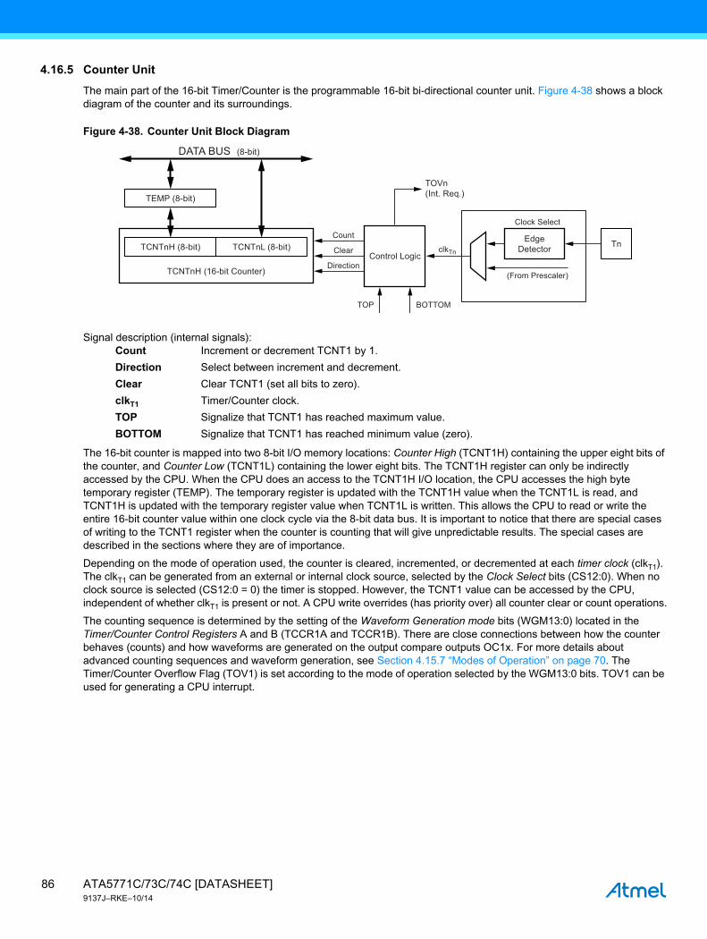
4.16.5 Counter Unit
The main part of the 16-bit Timer/Counter is the programmable 16-bit bi-directional counter unit. Figure 4-38 shows a block diagram of the counter and its surroundings.
Figure 4-38. Counter Unit Block Diagram
Signal description (internal signals):Count Increment or decrement TCNT1 by 1.
Direction Select between increment and decrement.
Clear Clear TCNT1 (set all bits to zero).
clkT1 Timer/Counter clock.
TOP Signalize that TCNT1 has reached maximum value.
BOTTOM Signalize that TCNT1 has reached minimum value (zero).
The 16-bit counter is mapped into two 8-bit I/O memory locations: Counter High (TCNT1H) containing the upper eight bits of the counter, and Counter Low (TCNT1L) containing the lower eight bits. The TCNT1H register can only be indirectly accessed by the CPU. When the CPU does an access to the TCNT1H I/O location, the CPU accesses the high byte temporary register (TEMP). The temporary register is updated with the TCNT1H value when the TCNT1L is read, and TCNT1H is updated with the temporary register value when TCNT1L is written. This allows the CPU to read or write the entire 16-bit counter value within one clock cycle via the 8-bit data bus. It is important to notice that there are special cases of writing to the TCNT1 register when the counter is counting that will give unpredictable results. The special cases are described in the sections where they are of importance.
Depending on the mode of operation used, the counter is cleared, incremented, or decremented at each timer clock (clkT1). The clkT1 can be generated from an external or internal clock source, selected by the Clock Select bits (CS12:0). When no clock source is selected (CS12:0 = 0) the timer is stopped. However, the TCNT1 value can be accessed by the CPU, independent of whether clkT1 is present or not. A CPU write overrides (has priority over) all counter clear or count operations.
The counting sequence is determined by the setting of the Waveform Generation mode bits (WGM13:0) located in the Timer/Counter Control Registers A and B (TCCR1A and TCCR1B). There are close connections between how the counter behaves (counts) and how waveforms are generated on the output compare outputs OC1x. For more details about advanced counting sequences and waveform generation, see Section 4.15.7 “Modes of Operation” on page 70. The Timer/Counter Overflow Flag (TOV1) is set according to the mode of operation selected by the WGM13:0 bits. TOV1 can be used for generating a CPU interrupt.
BOTTOMTOP
TOVn(Int. Req.)
DATA BUS (8-bit)
Control LogicTCNTnH (8-bit)
TCNTnH (16-bit Counter)
TCNTnL (8-bit)
TEMP (8-bit)
clkTnClear
Count
Direction
EdgeDetector
(From Prescaler)
Clock Select
Tn
ATA5771C/73C/74C [DATASHEET]9137J–RKE–10/14
86

4.16.6 Input Capture Unit
The Timer/Counter incorporates an input capture unit that can capture external events and give them a time-stamp indicating time of occurrence. The external signal indicating an event, or multiple events, can be applied via the ICP1 pin or alternatively, via the analog-comparator unit. The time-stamps can then be used to calculate frequency, duty-cycle, and other features of the signal applied. Alternatively the time-stamps can be used for creating a log of the events.
The input capture unit is illustrated by the block diagram shown in Figure 4-39. The elements of the block diagram that are not directly a part of the input capture unit are gray shaded. The small “n” in register and bit names indicates the Timer/Counter number.
Figure 4-39. Input Capture Unit Block Diagram
When a change of the logic level (an event) occurs on the Input Capture pin (ICP1), alternatively on the Analog Comparator output (ACO), and this change confirms to the setting of the edge detector, a capture will be triggered. When a capture is triggered, the 16-bit value of the counter (TCNT1) is written to the Input Capture Register (ICR1). The Input Capture Flag (ICF1) is set at the same system clock as the TCNT1 value is copied into ICR1 register. If enabled (ICIE1 = 1), the input capture flag generates an Input Capture interrupt. The ICF1 flag is automatically cleared when the interrupt is executed. Alternatively the ICF1 flag can be cleared by software by writing a logical one to its I/O bit location.
Reading the 16-bit value in the Input Capture Register (ICR1) is done by first reading the low byte (ICR1L) and then the high byte (ICR1H). When the low byte is read the high byte is copied into the high byte temporary register (TEMP). When the CPU reads the ICR1H I/O location it will access the TEMP register.
The ICR1 register can only be written when using a waveform generation mode that utilizes the ICR1 register for defining the counter’s TOP value. In these cases the Waveform Generation mode (WGM13:0) bits must be set before the TOP value can be written to the ICR1 register. When writing the ICR1 register the high byte must be written to the ICR1H I/O location before the low byte is written to ICR1L.
For more information on how to access the 16-bit registers refer to Section 4.16.3 “Accessing 16-bit Registers” on page 83.
ICFn (Int. Req.)
ICRnL (8-bit)ICRnH (8-bit)
ICRn (16-bit Register)
TEMP (8-bit)
TCNTnL (8-bit)TCNTnH (8-bit)
TCNTn (16-bit Counter)
DATA BUS (8-bit)
NoiseCanceler
AnalogComparator Edge
Detector
ICNCnACIC*ACO*
WRITE
+
-
ICESn
ICPn
87ATA5771C/73C/74C [DATASHEET]9137J–RKE–10/14

4.16.6.1 Input Capture Trigger Source
The main trigger source for the input capture unit is the Input Capture pin (ICP1). Timer/Counter1 can alternatively use the analog comparator output as trigger source for the input capture unit. The analog comparator is selected as trigger source by setting the Analog Comparator Input Capture (ACIC) bit in the Analog Comparator Control and Status Register (ACSR). Be aware that changing trigger source can trigger a capture. The input capture flag must therefore be cleared after the change.
Both the Input Capture pin (ICP1) and the Analog Comparator output (ACO) inputs are sampled using the same technique as for the T1 pin (Figure 4-50 on page 105). The edge detector is also identical. However, when the noise canceler is enabled, additional logic is inserted before the edge detector, which increases the delay by four system clock cycles. Note that the input of the noise canceler and edge detector is always enabled unless the Timer/Counter is set in a waveform generation mode that uses ICR1 to define TOP.
An input capture can be triggered by software by controlling the port of the ICP1 pin.
4.16.6.2 Noise Canceler
The noise canceler improves noise immunity by using a simple digital filtering scheme. The noise canceler input is monitored over four samples, and all four must be equal for changing the output that in turn is used by the edge detector.
The noise canceler is enabled by setting the Input Capture Noise Canceler (ICNC1) bit in Timer/Counter Control Register B (TCCR1B). When enabled the noise canceler introduces additional four system clock cycles of delay from a change applied to the input, to the update of the ICR1 Register. The noise canceler uses the system clock and is therefore not affected by the prescaler.
4.16.6.3 Using the Input Capture Unit
The main challenge when using the input capture unit is to assign enough processor capacity for handling the incoming events. The time between two events is critical. If the processor has not read the captured value in the ICR1 register before the next event occurs, the ICR1 will be overwritten with a new value. In this case the result of the capture will be incorrect.
When using the input capture interrupt, the ICR1 register should be read as early in the interrupt handler routine as possible. Even though the input capture interrupt has relatively high priority, the maximum interrupt response time is dependent on the maximum number of clock cycles it takes to handle any of the other interrupt requests.
Using the input capture unit in any mode of operation when the TOP value (resolution) is actively changed during operation, is not recommended.
Measurement of an external signal’s duty cycle requires that the trigger edge is changed after each capture. Changing the edge sensing must be done as early as possible after the ICR1 register has been read. After a change of the edge, the input capture flag (ICF1) must be cleared by software (writing a logical one to the I/O bit location). For measuring frequency only, the clearing of the ICF1 flag is not required (if an interrupt handler is used).
4.16.7 Output Compare Units
The 16-bit comparator continuously compares TCNT1 with the Output Compare Register (OCR1x). If TCNT equals OCR1x the comparator signals a match. A match will set the Output Compare Flag (OCF1x) at the next timer clock cycle. If enabled (OCIE1x = 1), the output compare flag generates an output compare interrupt. The OCF1x flag is automatically cleared when the interrupt is executed. Alternatively the OCF1x flag can be cleared by software by writing a logical one to its I/O bit location. The waveform generator uses the match signal to generate an output according to operating mode set by the Waveform Generation mode (WGM13:0) bits and Compare Output mode (COM1x1:0) bits. The TOP and BOTTOM signals are used by the waveform generator for handling the special cases of the extreme values in some modes of operation (Section 4.15.7 “Modes of Operation” on page 70).
A special feature of output compare unit A allows it to define the Timer/Counter TOP value (i.e., counter resolution). In addition to the counter resolution, the TOP value defines the period time for waveforms generated by the waveform generator.
Figure 4-40 shows a block diagram of the output compare unit. The small “n” in the register and bit names indicates the device number (n = 1 for Timer/Counter 1), and the “x” indicates output compare unit (A/B). The elements of the block diagram that are not directly a part of the output compare unit are gray shaded.
ATA5771C/73C/74C [DATASHEET]9137J–RKE–10/14
88
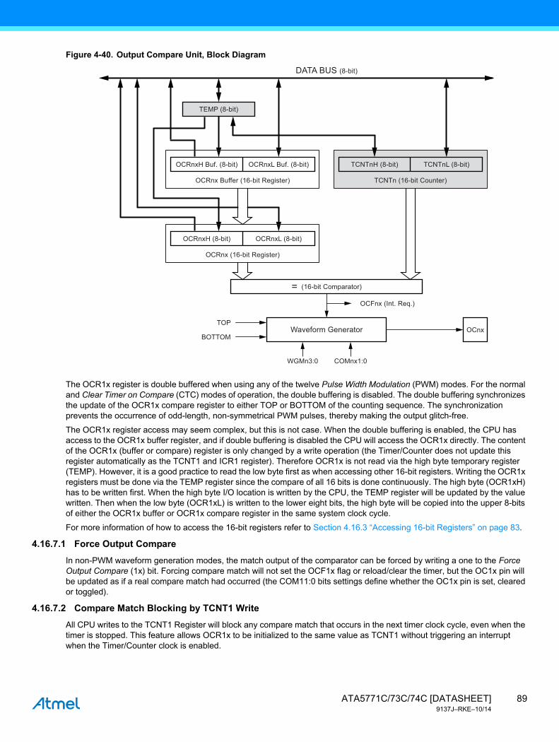
Figure 4-40. Output Compare Unit, Block Diagram
The OCR1x register is double buffered when using any of the twelve Pulse Width Modulation (PWM) modes. For the normal and Clear Timer on Compare (CTC) modes of operation, the double buffering is disabled. The double buffering synchronizes the update of the OCR1x compare register to either TOP or BOTTOM of the counting sequence. The synchronization prevents the occurrence of odd-length, non-symmetrical PWM pulses, thereby making the output glitch-free.
The OCR1x register access may seem complex, but this is not case. When the double buffering is enabled, the CPU has access to the OCR1x buffer register, and if double buffering is disabled the CPU will access the OCR1x directly. The content of the OCR1x (buffer or compare) register is only changed by a write operation (the Timer/Counter does not update this register automatically as the TCNT1 and ICR1 register). Therefore OCR1x is not read via the high byte temporary register (TEMP). However, it is a good practice to read the low byte first as when accessing other 16-bit registers. Writing the OCR1x registers must be done via the TEMP register since the compare of all 16 bits is done continuously. The high byte (OCR1xH) has to be written first. When the high byte I/O location is written by the CPU, the TEMP register will be updated by the value written. Then when the low byte (OCR1xL) is written to the lower eight bits, the high byte will be copied into the upper 8-bits of either the OCR1x buffer or OCR1x compare register in the same system clock cycle.
For more information of how to access the 16-bit registers refer to Section 4.16.3 “Accessing 16-bit Registers” on page 83.
4.16.7.1 Force Output Compare
In non-PWM waveform generation modes, the match output of the comparator can be forced by writing a one to the Force Output Compare (1x) bit. Forcing compare match will not set the OCF1x flag or reload/clear the timer, but the OC1x pin will be updated as if a real compare match had occurred (the COM11:0 bits settings define whether the OC1x pin is set, cleared or toggled).
4.16.7.2 Compare Match Blocking by TCNT1 Write
All CPU writes to the TCNT1 Register will block any compare match that occurs in the next timer clock cycle, even when the timer is stopped. This feature allows OCR1x to be initialized to the same value as TCNT1 without triggering an interrupt when the Timer/Counter clock is enabled.
OCRnxL Buf. (8-bit)OCRnxH Buf. (8-bit)
OCRnx Buffer (16-bit Register)
TEMP (8-bit)
OCRnxL (8-bit)
OCFnx (Int. Req.)
OCRnxH (8-bit)
OCRnx (16-bit Register)
= (16-bit Comparator)
WGMn3:0 COMnx1:0
Waveform Generator
TCNTnL (8-bit)TCNTnH (8-bit)
TCNTn (16-bit Counter)
DATA BUS (8-bit)
OCnxTOP
BOTTOM
89ATA5771C/73C/74C [DATASHEET]9137J–RKE–10/14

4.16.7.3 Using the Output Compare Unit
Since writing TCNT1 in any mode of operation will block all compare matches for one timer clock cycle, there are risks involved when changing TCNT1 when using any of the output compare channels, independent of whether the Timer/Counter is running or not. If the value written to TCNT1 equals the OCR1x value, the compare match will be missed, resulting in incorrect waveform generation. Do not write the TCNT1 equal to TOP in PWM modes with variable TOP values. The compare match for the TOP will be ignored and the counter will continue to 0xFFFF. Similarly, do not write the TCNT1 value equal to BOTTOM when the counter is downcounting.
The setup of the OC1x should be performed before setting the data direction register for the port pin to output. The easiest way of setting the OC1x value is to use the force output compare (1x) strobe bits in normal mode. The OC1x register keeps its value even when changing between waveform generation modes.
Be aware that the COM1x1:0 bits are not double buffered together with the compare value. Changing the COM1x1:0 bits will take effect immediately.
4.16.8 Compare Match Output Unit
The Compare Output mode (COM1x1:0) bits have two functions. The waveform generator uses the COM1x1:0 bits for defining the output compare (OC1x) state at the next compare match. Secondly the COM1x1:0 bits control the OC1x pin output source. Figure 4-41 shows a simplified schematic of the logic affected by the COM1x1:0 bit setting. The I/O registers, I/O bits, and I/O pins in the figure are shown in bold. Only the parts of the general I/O port control registers (DDR and PORT) that are affected by the COM1x1:0 bits are shown. When referring to the OC1x state, the reference is for the internal OC1x Register, not the OC1x pin. If a system reset occur, the OC1x register is reset to “0”.
Figure 4-41. Compare Match Output Unit, Schematic
The general I/O port function is overridden by the output compare (OC1x) from the waveform generator if either of the COM1x1:0 bits are set. However, the OC1x pin direction (input or output) is still controlled by the Data Direction Register (DDR) for the port pin. The data direction register bit for the OC1x pin (DDR_OC1x) must be set as output before the OC1x value is visible on the pin. The port override function is generally independent of the waveform generation mode, but there are some exceptions. See Table 4-40 on page 99, Table 4-41 on page 99 and Table 4-42 on page 100 for details.
The design of the output compare pin logic allows initialization of the OC1x state before the output is enabled. Note that some COM1x1:0 bit settings are reserved for certain modes of operation. See Section 4.11.5 “Register Description” on page 44.
The COM1x1:0 bits have no effect on the Input Capture unit.
DAT
A B
US
0
1
QD
COMnx1
COMnx0
FOCnx
OCnx
WaveformGenerator
QD
PORT
QD
DDR
OCnxPin
clkI/O
ATA5771C/73C/74C [DATASHEET]9137J–RKE–10/14
90
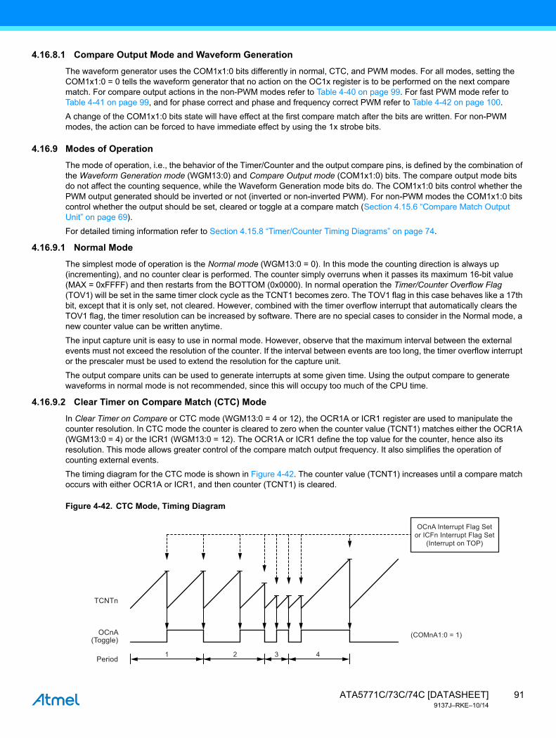
4.16.8.1 Compare Output Mode and Waveform Generation
The waveform generator uses the COM1x1:0 bits differently in normal, CTC, and PWM modes. For all modes, setting the COM1x1:0 = 0 tells the waveform generator that no action on the OC1x register is to be performed on the next compare match. For compare output actions in the non-PWM modes refer to Table 4-40 on page 99. For fast PWM mode refer to Table 4-41 on page 99, and for phase correct and phase and frequency correct PWM refer to Table 4-42 on page 100.
A change of the COM1x1:0 bits state will have effect at the first compare match after the bits are written. For non-PWM modes, the action can be forced to have immediate effect by using the 1x strobe bits.
4.16.9 Modes of Operation
The mode of operation, i.e., the behavior of the Timer/Counter and the output compare pins, is defined by the combination of the Waveform Generation mode (WGM13:0) and Compare Output mode (COM1x1:0) bits. The compare output mode bits do not affect the counting sequence, while the Waveform Generation mode bits do. The COM1x1:0 bits control whether the PWM output generated should be inverted or not (inverted or non-inverted PWM). For non-PWM modes the COM1x1:0 bits control whether the output should be set, cleared or toggle at a compare match (Section 4.15.6 “Compare Match Output Unit” on page 69).
For detailed timing information refer to Section 4.15.8 “Timer/Counter Timing Diagrams” on page 74.
4.16.9.1 Normal Mode
The simplest mode of operation is the Normal mode (WGM13:0 = 0). In this mode the counting direction is always up (incrementing), and no counter clear is performed. The counter simply overruns when it passes its maximum 16-bit value (MAX = 0xFFFF) and then restarts from the BOTTOM (0x0000). In normal operation the Timer/Counter Overflow Flag (TOV1) will be set in the same timer clock cycle as the TCNT1 becomes zero. The TOV1 flag in this case behaves like a 17th bit, except that it is only set, not cleared. However, combined with the timer overflow interrupt that automatically clears the TOV1 flag, the timer resolution can be increased by software. There are no special cases to consider in the Normal mode, a new counter value can be written anytime.
The input capture unit is easy to use in normal mode. However, observe that the maximum interval between the external events must not exceed the resolution of the counter. If the interval between events are too long, the timer overflow interrupt or the prescaler must be used to extend the resolution for the capture unit.
The output compare units can be used to generate interrupts at some given time. Using the output compare to generate waveforms in normal mode is not recommended, since this will occupy too much of the CPU time.
4.16.9.2 Clear Timer on Compare Match (CTC) Mode
In Clear Timer on Compare or CTC mode (WGM13:0 = 4 or 12), the OCR1A or ICR1 register are used to manipulate the counter resolution. In CTC mode the counter is cleared to zero when the counter value (TCNT1) matches either the OCR1A (WGM13:0 = 4) or the ICR1 (WGM13:0 = 12). The OCR1A or ICR1 define the top value for the counter, hence also its resolution. This mode allows greater control of the compare match output frequency. It also simplifies the operation of counting external events.
The timing diagram for the CTC mode is shown in Figure 4-42. The counter value (TCNT1) increases until a compare match occurs with either OCR1A or ICR1, and then counter (TCNT1) is cleared.
Figure 4-42. CTC Mode, Timing Diagram
1 2
TCNTn
(COMnA1:0 = 1)OCnA(Toggle)
Period3
OCnA Interrupt Flag Setor ICFn Interrupt Flag Set
(Interrupt on TOP)
4
91ATA5771C/73C/74C [DATASHEET]9137J–RKE–10/14

An interrupt can be generated at each time the counter value reaches the TOP value by either using the OCF1A or ICF1 flag according to the register used to define the TOP value. If the interrupt is enabled, the interrupt handler routine can be used for updating the TOP value. However, changing the TOP to a value close to BOTTOM when the counter is running with none or a low prescaler value must be done with care since the CTC mode does not have the double buffering feature. If the new value written to OCR1A or ICR1 is lower than the current value of TCNT1, the counter will miss the compare match. The counter will then have to count to its maximum value (0xFFFF) and wrap around starting at 0x0000 before the compare match can occur. In many cases this feature is not desirable. An alternative will then be to use the fast PWM mode using OCR1A for defining TOP (WGM13:0 = 15) since the OCR1A then will be double buffered.
For generating a waveform output in CTC mode, the OC1A output can be set to toggle its logical level on each compare match by setting the compare output mode bits to toggle mode (COM1A1:0 = 1). The OC1A value will not be visible on the port pin unless the data direction for the pin is set to output (DDR_OC1A = 1). The waveform generated will have a maximum frequency of 1A = fclk_I/O/2 when OCR1A is set to zero (0x0000). The waveform frequency is defined by the following equation:
The N variable represents the prescaler factor (1, 8, 64, 256, or 1024).
As for the normal mode of operation, the TOV1 flag is set in the same timer clock cycle that the counter counts from MAX to 0x0000.
4.16.9.3 Fast PWM Mode
The fast Pulse Width Modulation or fast PWM mode (WGM13:0 = 5, 6, 7, 14, or 15) provides a high frequency PWM waveform generation option. The fast PWM differs from the other PWM options by its single-slope operation. The counter counts from BOTTOM to TOP then restarts from BOTTOM. In non-inverting compare output mode, the output compare (OC1x) is cleared on the compare match between TCNT1 and OCR1x, and set at BOTTOM. In inverting compare output mode output is set on compare match and cleared at BOTTOM. Due to the single-slope operation, the operating frequency of the fast PWM mode can be twice as high as the phase correct and phase and frequency correct PWM modes that use dual-slope operation. This high frequency makes the fast PWM mode well suited for power regulation, rectification, and DAC applications. High frequency allows physically small sized external components (coils, capacitors), hence reduces total system cost.
The PWM resolution for fast PWM can be fixed to 8-, 9-, or 10-bit, or defined by either ICR1 or OCR1A. The minimum resolution allowed is 2-bit (ICR1 or OCR1A set to 0x0003), and the maximum resolution is 16-bit (ICR1 or OCR1A set to MAX). The PWM resolution in bits can be calculated by using the following equation:
In fast PWM mode the counter is incremented until the counter value matches either one of the fixed values 0x00FF, 0x01FF, or 0x03FF (WGM13:0 = 5, 6, or 7), the value in ICR1 (WGM13:0 = 14), or the value in OCR1A (WGM13:0 = 15). The counter is then cleared at the following timer clock cycle. The timing diagram for the fast PWM mode is shown in Figure 4-43. The figure shows fast PWM mode when OCR1A or ICR1 is used to define TOP. The TCNT1 value is in the timing diagram shown as a histogram for illustrating the single-slope operation. The diagram includes non-inverted and inverted PWM outputs. The small horizontal line marks on the TCNT1 slopes represent compare matches between OCR1x and TCNT1. The OC1x interrupt flag will be set when a compare match occurs.
fOCnAfclk_I/O
2 N 1 OCRnA+( )⋅ ⋅--------------------------------------------------=
RFPWMTOP 1+( )log2( )log
----------------------------------=
ATA5771C/73C/74C [DATASHEET]9137J–RKE–10/14
92

Figure 4-43. Fast PWM Mode, Timing Diagram
The Timer/Counter overflow flag (TOV1) is set each time the counter reaches TOP. In addition the OC1A or ICF1 flag is set at the same timer clock cycle as TOV1 is set when either OCR1A or ICR1 is used for defining the TOP value. If one of the interrupts are enabled, the interrupt handler routine can be used for updating the TOP and compare values.
When changing the TOP value the program must ensure that the new TOP value is higher or equal to the value of all of the compare registers. If the TOP value is lower than any of the compare registers, a compare match will never occur between the TCNT1 and the OCR1x. Note that when using fixed TOP values the unused bits are masked to zero when any of the OCR1x registers are written.
The procedure for updating ICR1 differs from updating OCR1A when used for defining the TOP value. The ICR1 register is not double buffered. This means that if ICR1 is changed to a low value when the counter is running with none or a low prescaler value, there is a risk that the new ICR1 value written is lower than the current value of TCNT1. The result will then be that the counter will miss the compare match at the TOP value. The counter will then have to count to the MAX value (0xFFFF) and wrap around starting at 0x0000 before the compare match can occur. The OCR1A register however, is double buffered. This feature allows the OCR1A I/O location to be written anytime. When the OCR1A I/O location is written the value written will be put into the OCR1A buffer register. The OCR1A compare register will then be updated with the value in the buffer register at the next timer clock cycle the TCNT1 matches TOP. The update is done at the same timer clock cycle as the TCNT1 is cleared and the TOV1 flag is set.
Using the ICR1 register for defining TOP works well when using fixed TOP values. By using ICR1, the OCR1A register is free to be used for generating a PWM output on OC1A. However, if the base PWM frequency is actively changed (by changing the TOP value), using the OCR1A as TOP is clearly a better choice due to its double buffer feature.
In fast PWM mode, the compare units allow generation of PWM waveforms on the OC1x pins. Setting the COM1x1:0 bits to two will produce a non-inverted PWM and an inverted PWM output can be generated by setting the COM1x1:0 to three (see Table 4-41 on page 99). The actual OC1x value will only be visible on the port pin if the data direction for the port pin is set as output (DDR_OC1x). The PWM waveform is generated by setting (or clearing) the OC1x register at the compare match between OCR1x and TCNT1, and clearing (or setting) the OC1x register at the timer clock cycle the counter is cleared (changes from TOP to BOTTOM).
The PWM frequency for the output can be calculated by the following equation:
The N variable represents the prescaler divider (1, 8, 64, 256, or 1024).
The extreme values for the OCR1x register represents special cases when generating a PWM waveform output in the fast PWM mode. If the OCR1x is set equal to BOTTOM (0x0000) the output will be a narrow spike for each TOP+1 timer clock cycle. Setting the OCR1x equal to TOP will result in a constant high or low output (depending on the polarity of the output set by the COM1x1:0 bits.)
1 2 3 4 5
TCNTn
(COMnx1:0 = 2)OCnx
OCnx
Period
OCRnx/ TOP Update andTOVn Interrupt Flag Set and
OCnA Interrupt Flag Setor ICFn Interrupt Flag Set
(Interrupt on TOP)
6 7 8
(COMnx1:0 = 3)
fOCnxPWMfclk_I/O
N 1 TOP+( )⋅----------------------------------=
93ATA5771C/73C/74C [DATASHEET]9137J–RKE–10/14
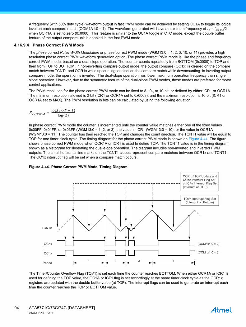
A frequency (with 50% duty cycle) waveform output in fast PWM mode can be achieved by setting OC1A to toggle its logical level on each compare match (COM1A1:0 = 1). The waveform generated will have a maximum frequency of 1A = fclk_I/O/2 when OCR1A is set to zero (0x0000). This feature is similar to the OC1A toggle in CTC mode, except the double buffer feature of the output compare unit is enabled in the fast PWM mode.
4.16.9.4 Phase Correct PWM Mode
The phase correct Pulse Width Modulation or phase correct PWM mode (WGM13:0 = 1, 2, 3, 10, or 11) provides a high resolution phase correct PWM waveform generation option. The phase correct PWM mode is, like the phase and frequency correct PWM mode, based on a dual-slope operation. The counter counts repeatedly from BOTTOM (0x0000) to TOP and then from TOP to BOTTOM. In non-inverting compare output mode, the output compare (OC1x) is cleared on the compare match between TCNT1 and OCR1x while upcounting, and set on the compare match while downcounting. In inverting output compare mode, the operation is inverted. The dual-slope operation has lower maximum operation frequency than single slope operation. However, due to the symmetric feature of the dual-slope PWM modes, these modes are preferred for motor control applications.
The PWM resolution for the phase correct PWM mode can be fixed to 8-, 9-, or 10-bit, or defined by either ICR1 or OCR1A. The minimum resolution allowed is 2-bit (ICR1 or OCR1A set to 0x0003), and the maximum resolution is 16-bit (ICR1 or OCR1A set to MAX). The PWM resolution in bits can be calculated by using the following equation:
In phase correct PWM mode the counter is incremented until the counter value matches either one of the fixed values 0x00FF, 0x01FF, or 0x03FF (WGM13:0 = 1, 2, or 3), the value in ICR1 (WGM13:0 = 10), or the value in OCR1A (WGM13:0 = 11). The counter has then reached the TOP and changes the count direction. The TCNT1 value will be equal to TOP for one timer clock cycle. The timing diagram for the phase correct PWM mode is shown on Figure 4-44. The figure shows phase correct PWM mode when OCR1A or ICR1 is used to define TOP. The TCNT1 value is in the timing diagram shown as a histogram for illustrating the dual-slope operation. The diagram includes non-inverted and inverted PWM outputs. The small horizontal line marks on the TCNT1 slopes represent compare matches between OCR1x and TCNT1. The OC1x interrupt flag will be set when a compare match occurs.
Figure 4-44. Phase Correct PWM Mode, Timing Diagram
The Timer/Counter Overflow Flag (TOV1) is set each time the counter reaches BOTTOM. When either OCR1A or ICR1 is used for defining the TOP value, the OC1A or ICF1 flag is set accordingly at the same timer clock cycle as the OCR1x registers are updated with the double buffer value (at TOP). The interrupt flags can be used to generate an interrupt each time the counter reaches the TOP or BOTTOM value.
RPCPWMTOP 1+( )log2( )log
----------------------------------=
1 2 3 4
TCNTn
(COMnx1:0 = 2)
(COMnx1:0 = 3)
OCnx
OCnx
Period
TOVn Interrupt Flag Set(Interrupt on Bottom)
OCRnx/ TOP Update andOCnA Interrupt Flag Setor ICFn Interrupt Flag Set(Interrupt on TOP)
ATA5771C/73C/74C [DATASHEET]9137J–RKE–10/14
94

When changing the TOP value the program must ensure that the new TOP value is higher or equal to the value of all of the compare registers. If the TOP value is lower than any of the compare registers, a compare match will never occur between the TCNT1 and the OCR1x. Note that when using fixed TOP values, the unused bits are masked to zero when any of the OCR1x registers are written. As the third period shown in Figure 4-44 on page 94 illustrates, changing the TOP actively while the Timer/Counter is running in the phase correct mode can result in an unsymmetrical output. The reason for this can be found in the time of update of the OCR1x Register. Since the OCR1x update occurs at TOP, the PWM period starts and ends at TOP. This implies that the length of the falling slope is determined by the previous TOP value, while the length of the rising slope is determined by the new TOP value. When these two values differ the two slopes of the period will differ in length. The difference in length gives the unsymmetrical result on the output.
It is recommended to use the phase and frequency correct mode instead of the phase correct mode when changing the TOP value while the Timer/Counter is running. When using a static TOP value there are practically no differences between the two modes of operation.
In phase correct PWM mode, the compare units allow generation of PWM waveforms on the OC1x pins. Setting the COM1x1:0 bits to two will produce a non-inverted PWM and an inverted PWM output can be generated by setting the COM1x1:0 to three (See Table 4-42 on page 100). The actual OC1x value will only be visible on the port pin if the data direction for the port pin is set as output (DDR_OC1x). The PWM waveform is generated by setting (or clearing) the OC1x register at the compare match between OCR1x and TCNT1 when the counter increments, and clearing (or setting) the OC1x Register at compare match between OCR1x and TCNT1 when the counter decrements. The PWM frequency for the output when using phase correct PWM can be calculated by the following equation:
The N variable represents the prescaler divider (1, 8, 64, 256, or 1024).
The extreme values for the OCR1x register represent special cases when generating a PWM waveform output in the phase correct PWM mode. If the OCR1x is set equal to BOTTOM the output will be continuously low and if set equal to TOP the output will be continuously high for non-inverted PWM mode. For inverted PWM the output will have the opposite logic values.
4.16.9.5 Phase and Frequency Correct PWM Mode
The phase and frequency correct Pulse Width Modulation, or phase and frequency correct PWM mode (WGM13:0 = 8 or 9) provides a high resolution phase and frequency correct PWM waveform generation option. The phase and frequency correct PWM mode is, like the phase correct PWM mode, based on a dual-slope operation. The counter counts repeatedly from BOTTOM (0x0000) to TOP and then from TOP to BOTTOM. In non-inverting compare output mode, the output compare (OC1x) is cleared on the compare match between TCNT1 and OCR1x while upcounting, and set on the compare match while downcounting. In inverting compare output mode, the operation is inverted. The dual-slope operation gives a lower maximum operation frequency compared to the single-slope operation. However, due to the symmetric feature of the dual-slope PWM modes, these modes are preferred for motor control applications.
The main difference between the phase correct, and the phase and frequency correct PWM mode is the time the OCR1x register is updated by the OCR1x buffer register, (see Figure 4-44 on page 94 and Figure 4-45 on page 96).
The PWM resolution for the phase and frequency correct PWM mode can be defined by either ICR1 or OCR1A. The minimum resolution allowed is 2-bit (ICR1 or OCR1A set to 0x0003), and the maximum resolution is 16-bit (ICR1 or OCR1A set to MAX). The PWM resolution in bits can be calculated using the following equation:
In phase and frequency correct PWM mode the counter is incremented until the counter value matches either the value in ICR1 (WGM13:0 = 8), or the value in OCR1A (WGM13:0 = 9). The counter has then reached the TOP and changes the count direction. The TCNT1 value will be equal to TOP for one timer clock cycle. The timing diagram for the phase correct and frequency correct PWM mode is shown on Figure 4-45 on page 96. The figure shows phase and frequency correct PWM mode when OCR1A or ICR1 is used to define TOP. The TCNT1 value is in the timing diagram shown as a histogram for illustrating the dual-slope operation. The diagram includes non-inverted and inverted PWM outputs. The small horizontal line marks on the TCNT1 slopes represent compare matches between OCR1x and TCNT1. The OC1x interrupt flag will be set when a compare match occurs.
fOCnxPCPWMfclk_I/O
2 N TOP⋅ ⋅----------------------------=
RPFCPWMTOP 1+( )log2( )log
----------------------------------=
95ATA5771C/73C/74C [DATASHEET]9137J–RKE–10/14
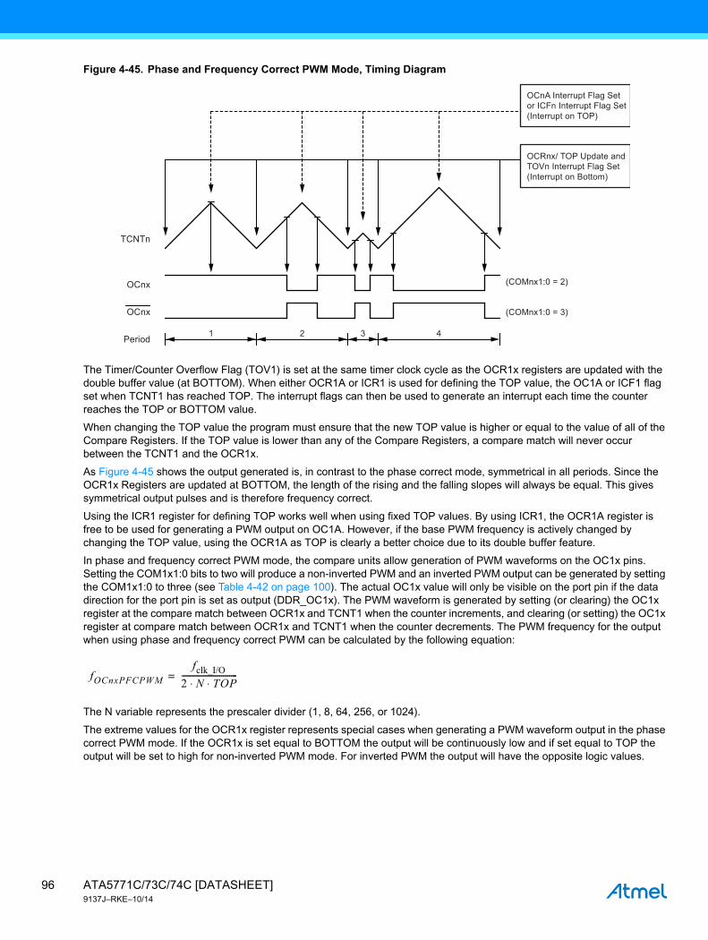
Figure 4-45. Phase and Frequency Correct PWM Mode, Timing Diagram
The Timer/Counter Overflow Flag (TOV1) is set at the same timer clock cycle as the OCR1x registers are updated with the double buffer value (at BOTTOM). When either OCR1A or ICR1 is used for defining the TOP value, the OC1A or ICF1 flag set when TCNT1 has reached TOP. The interrupt flags can then be used to generate an interrupt each time the counter reaches the TOP or BOTTOM value.
When changing the TOP value the program must ensure that the new TOP value is higher or equal to the value of all of the Compare Registers. If the TOP value is lower than any of the Compare Registers, a compare match will never occur between the TCNT1 and the OCR1x.
As Figure 4-45 shows the output generated is, in contrast to the phase correct mode, symmetrical in all periods. Since the OCR1x Registers are updated at BOTTOM, the length of the rising and the falling slopes will always be equal. This gives symmetrical output pulses and is therefore frequency correct.
Using the ICR1 register for defining TOP works well when using fixed TOP values. By using ICR1, the OCR1A register is free to be used for generating a PWM output on OC1A. However, if the base PWM frequency is actively changed by changing the TOP value, using the OCR1A as TOP is clearly a better choice due to its double buffer feature.
In phase and frequency correct PWM mode, the compare units allow generation of PWM waveforms on the OC1x pins. Setting the COM1x1:0 bits to two will produce a non-inverted PWM and an inverted PWM output can be generated by setting the COM1x1:0 to three (see Table 4-42 on page 100). The actual OC1x value will only be visible on the port pin if the data direction for the port pin is set as output (DDR_OC1x). The PWM waveform is generated by setting (or clearing) the OC1x register at the compare match between OCR1x and TCNT1 when the counter increments, and clearing (or setting) the OC1x register at compare match between OCR1x and TCNT1 when the counter decrements. The PWM frequency for the output when using phase and frequency correct PWM can be calculated by the following equation:
The N variable represents the prescaler divider (1, 8, 64, 256, or 1024).
The extreme values for the OCR1x register represents special cases when generating a PWM waveform output in the phase correct PWM mode. If the OCR1x is set equal to BOTTOM the output will be continuously low and if set equal to TOP the output will be set to high for non-inverted PWM mode. For inverted PWM the output will have the opposite logic values.
1 2 3 4
TCNTn
(COMnx1:0 = 2)
(COMnx1:0 = 3)
OCnx
OCnx
Period
OCnA Interrupt Flag Setor ICFn Interrupt Flag Set(Interrupt on TOP)
OCRnx/ TOP Update andTOVn Interrupt Flag Set(Interrupt on Bottom)
fOCnxPFCPWMfclk_I/O
2 N TOP⋅ ⋅----------------------------=
ATA5771C/73C/74C [DATASHEET]9137J–RKE–10/14
96

4.16.10 Timer/Counter Timing Diagrams
The Timer/Counter is a synchronous design and the timer clock (clkT1) is therefore shown as a clock enable signal in the following figures. The figures include information on when interrupt flags are set, and when the OCR1x register is updated with the OCR1x buffer value (only for modes utilizing double buffering). Figure 4-46 shows a timing diagram for the setting of OCF1x.
Figure 4-46. Timer/Counter Timing Diagram, Setting of OCF1x, no Prescaling
Figure 4-47 shows the same timing data, but with the prescaler enabled.
Figure 4-47. Timer/Counter Timing Diagram, Setting of OCF1x, with Prescaler (fclk_I/O/8)
OCRnx - 1
clkI/O
(clkI/O/1)
TCNTn
OCRnx
OCFnx
clkTn
OCRnx
OCRnx Value
OCRnx + 1 OCRnx + 2
OCRnx - 1
clkI/O
(clkI/O/8)
TCNTn
OCRnx
OCFnx
clkTn
OCRnx OCRnx + 1
OCRnx Value
OCRnx + 2
97ATA5771C/73C/74C [DATASHEET]9137J–RKE–10/14

Figure 4-48 shows the count sequence close to TOP in various modes. When using phase and frequency correct PWM mode the OCR1x register is updated at BOTTOM. The timing diagrams will be the same, but TOP should be replaced by BOTTOM, TOP-1 by BOTTOM+1 and so on. The same renaming applies for modes that set the TOV1 flag at BOTTOM.
Figure 4-48. Timer/Counter Timing Diagram, no Prescaling
Figure 4-49 shows the same timing data, but with the prescaler enabled.
Figure 4-49. Timer/Counter Timing Diagram, with Prescaler (fclk_I/O/8)
TOP - 1
clkI/O
(clkI/O/1)
TCNTn(CTC and FPWM)
OCRnx(Update at TOP)
TCNTn(PC and PFC PWM)
TOVn (FPWM)and ICFn
(if used as TOP)
clkTn
TOP
Old OCRnx Value New OCRnx Value
BOTTOM BOTTOM + 1
TOP - 1 TOP TOP - 1 TOP - 2
TOP - 1 TOP BOTTOM BOTTOM + 1
TOP - 1 TOP TOP - 1 TOP - 2
clkI/O
(clkI/O/8)
TCNTn(CTC and FPWM)
OCRnx(Update at TOP)
TCNTn(PC and PFC PWM)
TOVn (FPWM)and ICFn
(if used as TOP)
clkTn
Old OCRnx Value New OCRnx Value
ATA5771C/73C/74C [DATASHEET]9137J–RKE–10/14
98

4.16.11 Register Description
4.16.11.1 TCCR1A – Timer/Counter1 Control Register A
• Bit 7:6 – COM1A1:0: Compare Output Mode for Channel A
• Bit 5:4 – COM1B1:0: Compare Output Mode for Channel B
The COM1A1:0 and COM1B1:0 control the output compare pins (OC1A and OC1B respectively) behavior. If one or both of the COM1A1:0 bits are written to one, the OC1A output overrides the normal port functionality of the I/O pin it is connected to. If one or both of the COM1B1:0 bit are written to one, the OC1B output overrides the normal port functionality of the I/O pin it is connected to. However, note that the Data Direction Register (DDR) bit corresponding to the OC1A or OC1B pin must be set in order to enable the output driver.
When the OC1A or OC1B is connected to the pin, the function of the COM1x1:0 bits is dependent of the WGM13:0 bits setting. Table 4-40 shows the COM1x1:0 bit functionality when the WGM13:0 bits are set to a Normal or a CTC mode (non-PWM).
Table 4-41 shows the COM1x1:0 bit functionality when the WGM13:0 bits are set to the fast PWM mode.
Bit 7 6 5 4 3 2 1 0
0x2F (0x4F) COM1A1 COM1A0 COM1B1 COM1B0 – – WGM11 WGM10 TCCR1A
Read/Write R/W R/W R/W R/W R R R/W R/W
Initial Value 0 0 0 0 0 0 0 0
Table 4-40. Compare Output Mode, non-PWM
COM1A1/COM1B1 COM1A0/COM1B0 Description
0 0 Normal port operation, OC1A/OC1B disconnected.
0 1 Toggle OC1A/OC1B on compare match.
1 0 Clear OC1A/OC1B on compare match (set output to low level).
1 1 Set OC1A/OC1B on compare match (set output to high level).
Table 4-41. Compare Output Mode, Fast PWM(1)
COM1A1/COM1B1 COM1A0/COM1B0 Description
0 0 Normal port operation, OC1A/OC1B disconnected.
0 1WGM13=0: Normal port operation, OC1A/OC1B disconnected.
WGM13=1: Toggle OC1A on compare match, OC1B reserved.
1 0Clear OC1A/OC1B on compare match, set OC1A/OC1B at BOTTOM (non-inverting mode)
1 1Set OC1A/OC1B on compare match, clear OC1A/OC1B at BOTTOM (inverting mode)
Note: 1. A special case occurs when OCR1A/OCR1B equals TOP and COM1A1/COM1B1 is set. In this case the com-pare match is ignored, but the set or clear is done at BOTTOM. Section 4.15.7.3 “Fast PWM Mode” on page 72 for more details.
99ATA5771C/73C/74C [DATASHEET]9137J–RKE–10/14

Table 4-42 shows the COM1x1:0 bit functionality when the WGM13:0 bits are set to the phase correct or the phase and frequency correct, PWM mode.
Note: 1. A special case occurs when OCR1A/OCR1B equals TOP and COM1A1/COM1B1 is set. Section 4.16.9.4 “Phase Correct PWM Mode” on page 94 for more details.
• Bit 1:0 – WGM11:0: Waveform Generation Mode
Combined with the WGM13:2 bits found in the TCCR1B register, these bits control the counting sequence of the counter, the source for maximum (TOP) counter value, and what type of waveform generation to be used, see Table 4-43 on page 100. Modes of operation supported by the Timer/Counter unit are: Normal mode (counter), clear timer on compare match (CTC) mode, and three types of pulse width modulation (PWM) modes. (Section 4.16.9 “Modes of Operation” on page 91).
Note: 1. The CTC1 and PWM11:0 bit definition names are obsolete. Use the WGM12:0 definitions. However, the functionality and location of these bits are compatible with previous versions of the timer.
Table 4-42. Compare Output Mode, Phase Correct and Phase and Frequency Correct PWM(1)
COM1A1/COM1B1 COM1A0/COM1B0 Description
0 0 Normal port operation, OC1A/OC1B disconnected.
0 1WGM13=0: Normal port operation, OC1A/OC1B disconnected.
WGM13=1: Toggle OC1A on Compare Match, OC1B reserved.
1 0Clear OC1A/OC1B on compare match when up-counting. Set OC1A/OC1B on compare match when downcounting.
1 1Set OC1A/OC1B on compare match when up-counting. Clear OC1A/OC1B on compare match when downcounting.
Table 4-43. Waveform Generation Mode Bit Description(1)
Mode WGM13WGM12(CTC1)
WGM11(PWM11)
WGM10(PWM10)
Timer/Counter Mode of Operation TOP
Update of OCR1x at
TOV1 Flag Set on
0 0 0 0 0 Normal 0xFFFF Immediate MAX
1 0 0 0 1 PWM, phase correct, 8-bit 0x00FF TOP BOTTOM
2 0 0 1 0 PWM, phase correct, 9-bit 0x01FF TOP BOTTOM
3 0 0 1 1 PWM, phase correct, 10-bit 0x03FF TOP BOTTOM
4 0 1 0 0 CTC OCR1A Immediate MAX
5 0 1 0 1 Fast PWM, 8-bit 0x00FF BOTTOM TOP
6 0 1 1 0 Fast PWM, 9-bit 0x01FF BOTTOM TOP
7 0 1 1 1 Fast PWM, 10-bit 0x03FF BOTTOM TOP
8 1 0 0 0PWM, phase and frequency correct
ICR1 BOTTOM BOTTOM
9 1 0 0 1PWM, phase and frequency correct
OCR1A BOTTOM BOTTOM
10 1 0 1 0 PWM, phase correct ICR1 TOP BOTTOM
11 1 0 1 1 PWM, phase correct OCR1A TOP BOTTOM
12 1 1 0 0 CTC ICR1 Immediate MAX
13 1 1 0 1 (Reserved) – – –
14 1 1 1 0 Fast PWM ICR1 BOTTOM TOP
15 1 1 1 1 Fast PWM OCR1A BOTTOM TOP
ATA5771C/73C/74C [DATASHEET]9137J–RKE–10/14
100
4.16.11.2 TCCR1B – Timer/Counter1 Control Register B
• Bit 7 – ICNC1: Input Capture Noise Canceler
Setting this bit (to one) activates the input capture noise canceler. When the noise canceler is activated, the input from the input capture pin (ICP1) is filtered. The filter function requires four successive equal valued samples of the ICP1 pin for changing its output. The input capture is therefore delayed by four oscillator cycles when the noise canceler is enabled.
• Bit 6 – ICES1: Input Capture Edge Select
This bit selects which edge on the input capture pin (ICP1) that is used to trigger a capture event. When the ICES1 bit is written to zero, a falling (negative) edge is used as trigger, and when the ICES1 bit is written to one, a rising (positive) edge will trigger the capture.
When a capture is triggered according to the ICES1 setting, the counter value is copied into the input capture register (ICR1). The event will also set the input capture flag (ICF1), and this can be used to cause an input capture interrupt, if this interrupt is enabled.
When the ICR1 is used as TOP value (see description of the WGM13:0 bits located in the TCCR1A and the TCCR1B Register), the ICP1 is disconnected and consequently the Input Capture function is disabled.
• Bit 5 – Reserved Bit
This bit is reserved for future use. For ensuring compatibility with future devices, this bit must be written to zero when TCCR1B is written.
• Bit 4:3 – WGM13:2: Waveform Generation Mode
See TCCR1A register description.
• Bit 2:0 – CS12:0: Clock Select
The three clock select bits select the clock source to be used by the Timer/Counter, see Figure 4-33 on page 74 and Figure 4-34 on page 74.
If external pin modes are used for the Timer/Counter1, transitions on the T1 pin will clock the counter even if the pin is configured as an output. This feature allows software control of the counting.
Bit 7 6 5 4 3 2 1 0
0x2E (0x4E) ICNC1 ICES1 – WGM13 WGM12 CS12 CS11 CS10 TCCR1B
Read/Write R/W R/W R R/W R/W R/W R/W R/W
Initial Value 0 0 0 0 0 0 0 0
Table 4-44. Clock Select Bit Description
CS12 CS11 CS10 Description
0 0 0 No clock source (Timer/Counter stopped).
0 0 1 clkI/O/1 (no prescaling)
0 1 0 clkI/O/8 (from prescaler)
0 1 1 clkI/O/64 (from prescaler)
1 0 0 clkI/O/256 (from prescaler)
1 0 1 clkI/O/1024 (from prescaler)
1 1 0 External clock source on T1 pin. Clock on falling edge.
1 1 1 External clock source on T1 pin. Clock on rising edge.
101ATA5771C/73C/74C [DATASHEET]9137J–RKE–10/14

4.16.11.3 TCCR1C – Timer/Counter1 Control Register C
• Bit 7 – FOC1A: Force Output Compare for Channel A
• Bit 6 – FOC1B: Force Output Compare for Channel B
The FOC1A/FOC1B bits are only active when the WGM13:0 bits specifies a non-PWM mode. However, for ensuring compatibility with future devices, these bits must be set to zero when TCCR1A is written when operating in a PWM mode. When writing a logical one to the FOC1A/FOC1B bit, an immediate compare match is forced on the waveform generation unit. The OC1A/OC1B output is changed according to its COM1x1:0 bits setting. Note that the FOC1A/FOC1B bits are implemented as strobes. Therefore it is the value present in the COM1x1:0 bits that determine the effect of the forced compare.
A FOC1A/FOC1B strobe will not generate any interrupt nor will it clear the timer in clear timer on compare match (CTC) mode using OCR1A as TOP.
The FOC1A/FOC1B bits are always read as zero.
• Bit 5..0 – Reserved Bit
This bit is reserved for future use. For ensuring compatibility with future devices, this bit must be written to zero when the register is written.
4.16.11.4 TCNT1H and TCNT1L – Timer/Counter1
The two Timer/Counter I/O locations (TCNT1H and TCNT1L, combined TCNT1) give direct access, both for read and for write operations, to the Timer/Counter unit 16-bit counter. To ensure that both the high and low bytes are read and written simultaneously when the CPU accesses these registers, the access is performed using an 8-bit temporary high byte register (TEMP). This temporary register is shared by all the other 16-bit registers. See Section 4.16.3 “Accessing 16-bit Registers” on page 83.
Modifying the counter (TCNT1) while the counter is running introduces a risk of missing a compare match between TCNT1 and one of the OCR1x Registers.
Writing to the TCNT1 register blocks (removes) the compare match on the following timer clock for all compare units.
4.16.11.5 OCR1AH and OCR1AL – Output Compare Register 1 A
Bit 7 6 5 4 3 2 1 0
0x22 (0x42) FOC1A FOC1B – – – – – – TCCR1C
Read/Write W W R R R R R R
Initial Value 0 0 0 0 0 0 0 0
Bit 7 6 5 4 3 2 1 0
0x2D (0x4D) TCNT1[15:8] TCNT1H
0x2C (0x4C) TCNT1[7:0] TCNT1L
Read/Write R/W R/W R/W R/W R/W R/W R/W R/W
Initial Value 0 0 0 0 0 0 0 0
Bit 7 6 5 4 3 2 1 0
0x2B (0x4B) OCR1A[15:8] OCR1AH
0x2A (0x4A) OCR1A[7:0] OCR1AL
Read/Write R/W R/W R/W R/W R/W R/W R/W R/W
Initial Value 0 0 0 0 0 0 0 0
ATA5771C/73C/74C [DATASHEET]9137J–RKE–10/14
102
4.16.11.6 OCR1BH and OCR1BL – Output Compare Register 1 B
The output compare registers contain a 16-bit value that is continuously compared with the counter value (TCNT1). A match can be used to generate an output compare interrupt, or to generate a waveform output on the OC1x pin.
The output compare registers are 16-bit in size. To ensure that both the high and low bytes are written simultaneously when the CPU writes to these registers, the access is performed using an 8-bit temporary high byte register (TEMP). This temporary register is shared by all the other 16-bit registers. See Section 4.16.3 “Accessing 16-bit Registers” on page 83.
4.16.11.7 ICR1H and ICR1L – Input Capture Register 1
The input capture is updated with the counter (TCNT1) value each time an event occurs on the ICP1 pin (or optionally on the analog comparator output for Timer/Counter1). The input capture can be used for defining the counter TOP value.
The input capture register is 16-bit in size. To ensure that both the high and low bytes are read simultaneously when the CPU accesses these registers, the access is performed using an 8-bit temporary high byte register (TEMP). This temporary register is shared by all the other 16-bit registers. Section 4.16.3 “Accessing 16-bit Registers” on page 83.
4.16.11.8 TIMSK1 – Timer/Counter Interrupt Mask Register 1
• Bit 7,6,4,3 – Reserved Bit
This bit is reserved for future use. For ensuring compatibility with future devices, this bit must be written to zero when the register is written.
• Bit 5 – ICIE1: Timer/Counter1, Input Capture Interrupt Enable
When this bit is written to one, and the I-flag in the status register is set (interrupts globally enabled), the Timer/Counter input capture interrupt is enabled. The corresponding interrupt vector (see Section 4.12 “Interrupts” on page 47) is executed when the ICF1 Flag, located in TIFR1, is set.
• Bit 2– OCIE1B: Timer/Counter1, Output Compare B Match Interrupt Enable
When this bit is written to one, and the I-flag in the status register is set (interrupts globally enabled), the Timer/Counter1 Output Compare B match interrupt is enabled. The corresponding interrupt vector (see Section 4.12 “Interrupts” on page 47) is executed when the OCF1B flag, located in TIFR1, is set.
• Bit 1– OCIE1A: Timer/Counter1, Output Compare A Match Interrupt Enable
When this bit is written to one, and the I-flag in the status register is set (interrupts globally enabled), the Timer/Counter1 Output Compare A match interrupt is enabled. The corresponding Interrupt vector (see Section 4.12 “Interrupts” on page 47) is executed when the OCF1A flag, located in TIFR1, is set.
Bit 7 6 5 4 3 2 1 0
0x29 (0x49) OCR1B[15:8] OCR1BH
0x28 (0x48) OCR1B[7:0] OCR1BL
Read/Write R/W R/W R/W R/W R/W R/W R/W R/W
Initial Value 0 0 0 0 0 0 0 0
Bit 7 6 5 4 3 2 1 0
0x25 (0x45) ICR1[15:8] ICR1H
0x24 (0x44) ICR1[7:0] ICR1L
Read/Write R/W R/W R/W R/W R/W R/W R/W R/W
Initial Value 0 0 0 0 0 0 0 0
Bit 7 6 5 4 3 2 1 0
0x0C (0x2C) – – ICIE1 – – OCIE1B OCIE1A TOIE1 TIMSK1
Read/Write R R R/W R R R/W R/W R/W
Initial Value 0 0 0 0 0 0 0 0
103ATA5771C/73C/74C [DATASHEET]9137J–RKE–10/14

• Bit 0 – TOIE1: Timer/Counter1, Overflow Interrupt Enable
When this bit is written to one, and the I-flag in the status register is set (interrupts globally enabled), the Timer/Counter1 overflow interrupt is enabled. The corresponding interrupt vector (see Section 4.12 “Interrupts” on page 47) is executed when the TOV1 flag, located in TIFR1, is set.
4.16.11.9 TIFR1 – Timer/Counter Interrupt Flag Register 1
• Bit 7,6,4,3 – Reserved Bit
This bit is reserved for future use. For ensuring compatibility with future devices, this bit must be written to zero when the register is written.
• Bit 5– ICF1: Timer/Counter1, Input Capture Flag
This flag is set when a capture event occurs on the ICP1 pin. When the input capture register (ICR1) is set by the WGM13:0 to be used as the TOP value, the ICF1 flag is set when the counter reaches the TOP value.
ICF1 is automatically cleared when the input capture interrupt vector is executed. Alternatively, ICF1 can be cleared by writing a logic one to its bit location.
• Bit 2– OCF1B: Timer/Counter1, Output Compare B Match Flag
This flag is set in the timer clock cycle after the counter (TCNT1) value matches the output compare register B (OCR1B).
Note that a forced output compare (1B) strobe will not set the OCF1B flag.
OCF1B is automatically cleared when the output compare match B Interrupt Vector is executed. Alternatively, OCF1B can be cleared by writing a logic one to its bit location.
• Bit 1– OCF1A: Timer/Counter1, Output Compare A Match Flag
This flag is set in the timer clock cycle after the counter (TCNT1) value matches the output compare register A (OCR1A).
Note that a forced output compare (1A) strobe will not set the OCF1A flag.
OCF1A is automatically cleared when the output compare match A interrupt vector is executed. Alternatively, OCF1A can be cleared by writing a logic one to its bit location.
• Bit 0– TOV1: Timer/Counter1, Overflow Flag
The setting of this flag is dependent of the WGM13:0 bits setting. In normal and CTC modes, the TOV1 flag is set when the timer overflows. See Table 4-43 on page 100 for the TOV1 flag behavior when using another WGM13:0 bit setting.
TOV1 is automatically cleared when the Timer/Counter1 overflow interrupt vector is executed. Alternatively, TOV1 can be cleared by writing a logic one to its bit location.
Bit 7 6 5 4 3 2 1 0
0x0B (0x2B) – – ICIF1 – – OCF1B OCF1A TOV1 TIFR1
Read/Write R R R/W R R R/W R/W R/W
Initial Value 0 0 0 0 0 0 0 0
ATA5771C/73C/74C [DATASHEET]9137J–RKE–10/14
104
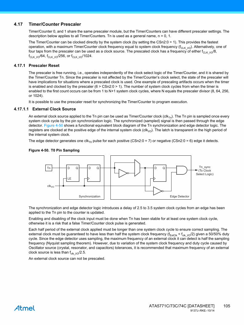
4.17 Timer/Counter Prescaler
Timer/Counter 0, and 1 share the same prescaler module, but the Timer/Counters can have different prescaler settings. The description below applies to all Timer/Counters. Tn is used as a general name, n = 0, 1.
The Timer/Counter can be clocked directly by the system clock (by setting the CSn2:0 = 1). This provides the fastest operation, with a maximum Timer/Counter clock frequency equal to system clock frequency (fCLK_I/O). Alternatively, one of four taps from the prescaler can be used as a clock source. The prescaled clock has a frequency of either fCLK_I/O/8, fCLK_I/O/64, fCLK_I/O/256, or fCLK_I/O/1024.
4.17.1 Prescaler Reset
The prescaler is free running, i.e., operates independently of the clock select logic of the Timer/Counter, and it is shared by the Timer/Counter Tn. Since the prescaler is not affected by the Timer/Counter’s clock select, the state of the prescaler will have implications for situations where a prescaled clock is used. One example of prescaling artifacts occurs when the timer is enabled and clocked by the prescaler (6 > CSn2:0 > 1). The number of system clock cycles from when the timer is enabled to the first count occurs can be from 1 to N+1 system clock cycles, where N equals the prescaler divisor (8, 64, 256, or 1024).
It is possible to use the prescaler reset for synchronizing the Timer/Counter to program execution.
4.17.1.1 External Clock Source
An external clock source applied to the Tn pin can be used as Timer/Counter clock (clkTn). The Tn pin is sampled once every system clock cycle by the pin synchronization logic. The synchronized (sampled) signal is then passed through the edge detector. Figure 4-50 shows a functional equivalent block diagram of the Tn synchronization and edge detector logic. The registers are clocked at the positive edge of the internal system clock (clkI/O). The latch is transparent in the high period of the internal system clock.
The edge detector generates one clkT0 pulse for each positive (CSn2:0 = 7) or negative (CSn2:0 = 6) edge it detects.
Figure 4-50. T0 Pin Sampling
The synchronization and edge detector logic introduces a delay of 2.5 to 3.5 system clock cycles from an edge has been applied to the Tn pin to the counter is updated.
Enabling and disabling of the clock input must be done when Tn has been stable for at least one system clock cycle, otherwise it is a risk that a false Timer/Counter clock pulse is generated.
Each half period of the external clock applied must be longer than one system clock cycle to ensure correct sampling. The external clock must be guaranteed to have less than half the system clock frequency (fExtClk < fclk_I/O/2) given a 50/50% duty cycle. Since the edge detector uses sampling, the maximum frequency of an external clock it can detect is half the sampling frequency (Nyquist sampling theorem). However, due to variation of the system clock frequency and duty cycle caused by Oscillator source (crystal, resonator, and capacitors) tolerances, it is recommended that maximum frequency of an external clock source is less than fclk_I/O/2.5.
An external clock source can not be prescaled.
Tn
Synchronization Edge Detector
Tn_sync(To Clock
Select Logic)
Q
LE
D QD QD
clkI/O
105ATA5771C/73C/74C [DATASHEET]9137J–RKE–10/14
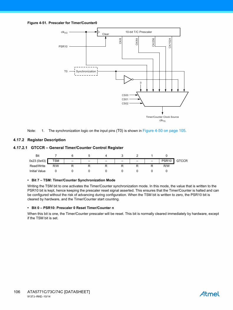
Figure 4-51. Prescaler for Timer/Counter0
Note: 1. The synchronization logic on the input pins (T0) is shown in Figure 4-50 on page 105.
4.17.2 Register Description
4.17.2.1 GTCCR – General Timer/Counter Control Register
• Bit 7 – TSM: Timer/Counter Synchronization Mode
Writing the TSM bit to one activates the Timer/Counter synchronization mode. In this mode, the value that is written to the PSR10 bit is kept, hence keeping the prescaler reset signal asserted. This ensures that the Timer/Counter is halted and can be configured without the risk of advancing during configuration. When the TSM bit is written to zero, the PSR10 bit is cleared by hardware, and the Timer/Counter start counting.
• Bit 0 – PSR10: Prescaler 0 Reset Timer/Counter n
When this bit is one, the Timer/Counter prescaler will be reset. This bit is normally cleared immediately by hardware, except if the TSM bit is set.
Timer/Counter Clock Source
clkI/O
PSR10
T0
10-bit T/C Prescaler
0
CS00
CK
/8
CK
/64
CK
/256
CK
/102
4
CS01CS02
Synchronization
Clear
clkT0
Bit 7 6 5 4 3 2 1 0
0x23 (0x43) TSM – – – – – – PSR10 GTCCR
Read/Write R/W R R R R R R R/W
Initial Value 0 0 0 0 0 0 0 0
ATA5771C/73C/74C [DATASHEET]9137J–RKE–10/14
106

4.18 USI – Universal Serial Interface
4.18.1 Features
● Two-wire synchronous data transfer (master or slave)
● Three-wire synchronous data transfer (master or slave)
● Data received interrupt
● Wakeup from idle mode
● In two-wire mode: wake-up from all sleep modes, including power-down mode
● Two-wire start condition detector with interrupt capability
4.18.2 Overview
The universal serial interface (USI), provides the basic hardware resources needed for serial communication. Combined with a minimum of control software, the USI allows significantly higher transfer rates and uses less code space than solutions based on software only. Interrupts are included to minimize the processor load.
A simplified block diagram of the USI is shown in Figure 4-52. For the actual placement of I/O pins. CPU accessible I/O Registers, including I/O bits and I/O pins, are shown in bold. The device-specific I/O Register and bit locations are listed in the Section 4.9.10 “Register Description” on page 33.
Figure 4-52. Universal Serial Interface, Block Diagram
The 8-bit shift register is directly accessible via the data bus and contains the incoming and outgoing data. The register has no buffering so the data must be read as quickly as possible to ensure that no data is lost. The most significant bit is connected to one of two output pins depending of the wire mode configuration. A transparent latch is inserted between the serial register output and output pin, which delays the change of data output to the opposite clock edge of the data input sampling. The serial input is always sampled from the Data Input (DI) pin independent of the configuration.
The 4-bit counter can be both read and written via the data bus, and can generate an overflow interrupt. Both the serial register and the counter are clocked simultaneously by the same clock source. This allows the counter to count the number of bits received or transmitted and generate an interrupt when the transfer is complete. Note that when an external clock source is selected the counter counts both clock edges. In this case the counter counts the number of edges, and not the number of bits. The clock can be selected from three different sources: The USCK pin, Timer/Counter0 compare match or from software.
The two-wire clock control unit can generate an interrupt when a start condition is detected on the two-wire bus. It can also generate wait states by holding the clock pin low after a start condition is detected, or after the counter overflows.
Q
32
10
LE
2
USIDR
D
TIM0 COMP
USCK/ SCL
Two-Wire ClockControl Unit
CLOCKHOLD
DAT
A B
US
[1]
Bit0
Bit7
US
ISIF
US
IOIF
US
IPF
US
IDC
USISR
4-bit Counter
DI/ SDA
DO (Output only)
(Input/ Open Drain))
(Input/ Open Drain))32
10
1
0
US
ISIE
US
IOIE
US
IWM
1
US
IWM
0
US
ICS
1
US
ICS
0
US
ICLK
US
ITC
USICR
107ATA5771C/73C/74C [DATASHEET]9137J–RKE–10/14

4.18.3 Functional Descriptions
4.18.3.1 Three-wire Mode
The USI three-wire mode is compliant to the serial peripheral interface (SPI) mode 0 and 1, but does not have the slave select (SS) pin functionality. However, this feature can be implemented in software if necessary. Pin names used by this mode are: DI, DO, and USCK.
Figure 4-53. Three-wire Mode Operation, Simplified Diagram
Figure 4-53 shows two USI units operating in three-wire mode, one as Master and one as slave. The two shift registers are interconnected in such way that after eight USCK clocks, the data in each register are interchanged. The same clock also increments the USI’s 4-bit counter. The counter overflow (interrupt) Flag, or USIOIF, can therefore be used to determine when a transfer is completed. The clock is generated by the Master device software by toggling the USCK pin via the PORT register or by writing a one to the USITC bit in USICR.
Figure 4-54. Three-wire Mode, Timing Diagram
The three-wire mode timing is shown in Figure 4-54. At the top of the figure is a USCK cycle reference. One bit is shifted into the USI shift register (USIDR) for each of these cycles. The USCK timing is shown for both external clock modes. In external clock mode 0 (USICS0 = 0), DI is sampled at positive edges, and DO is changed (data register is shifted by one) at negative edges. External clock mode 1 (USICS0 = 1) uses the opposite edges versus mode 0, i.e., samples data at negative and changes the output at positive edges. The USI clock modes corresponds to the SPI data mode 0 and 1.
Bit7 DI
USCK
USCK
DO
PORTxn
SLAVE
Bit6 Bit5 Bit4 Bit3 Bit2 Bit1 Bit0
Bit7 DI
DO
MASTER
Bit6 Bit5 Bit4 Bit3 Bit2 Bit1 Bit0
1 2
6MSB 5 4 3 2 1 LSB
3 4 5 6 7 8
6MSB
CYCLE (Reference)
USCK
USCK
5 4 3 2 1 LSB
A B C D E
DI
DO
ATA5771C/73C/74C [DATASHEET]9137J–RKE–10/14
108

Referring to the timing diagram (Figure 4-54), a bus transfer involves the following steps:
1. The slave device and master device sets up its data output and, depending on the protocol used, enables its out-put driver (mark A and B). The output is set up by writing the data to be transmitted to the serial data register. Enabling of the output is done by setting the corresponding bit in the port data direction register. Note that point A and B does not have any specific order, but both must be at least one half USCK cycle before point C where the data is sampled. This must be done to ensure that the data setup requirement is satisfied. The 4-bit counter is reset to zero.
2. The master generates a clock pulse by software toggling the USCK line twice (C and D). The bit value on the slave and master’s data input (DI) pin is sampled by the USI on the first edge (C), and the data output is changed on the opposite edge (D). The 4-bit counter will count both edges.
3. Step 2 is repeated eight times for a complete register (byte) transfer.
4. After eight clock pulses (i.e., 16 clock edges) the counter will overflow and indicate that the transfer is completed. The data bytes transferred must now be processed before a new transfer can be initiated. The overflow interrupt will wake up the processor if it is set to Idle mode. Depending of the protocol used the slave device can now set its output to high impedance.
4.18.3.2 SPI Master Operation Example
The following code demonstrates how to use the USI module as a SPI Master:SPITransfer:
out USIDR,r16ldi r16,(1<<USIOIF)out USISR,r16ldi r16,(1<<USIWM0)|(1<<USICS1)|(1<<USICLK)|(1<<USITC)
SPITransfer_loop:out USICR,r16in r16, USISRsbrs r16, USIOIFrjmp SPITransfer_loopin r16,USIDRret
The code is size optimized using only eight instructions (+ ret). The code example assumes that the DO and USCK pins are enabled as output in the DDRE Register. The value stored in register r16 prior to the function is called is transferred to the slave device, and when the transfer is completed the data received from the slave is stored back into the r16 register.
The second and third instructions clears the USI counter overflow flag and the USI counter value. The fourth and fifth instruction set three-wire mode, positive edge shift register clock, count at USITC strobe, and toggle USCK. The loop is repeated 16 times.
The following code demonstrates how to use the USI module as a SPI master with maximum speed (fsck = fck/4):SPITransfer_Fast:
out USIDR,r16ldi r16,(1<<USIWM0)|(0<<USICS0)|(1<<USITC)ldi r17,(1<<USIWM0)|(0<<USICS0)|(1<<USITC)|(1<<USICLK)
out USICR,r16;msBout USICR,r17out USICR,r16out USICR,r17out USICR,r16out USICR,r17out USICR,r16out USICR,r17out USICR,r16out USICR,r17out USICR,r16out USICR,r17out USICR,r16out USICR,r17
109ATA5771C/73C/74C [DATASHEET]9137J–RKE–10/14

out USICR,r16; LSBout USICR,r17
in r16,USIDRret
4.18.3.3 SPI Slave Operation Example
The following code demonstrates how to use the USI module as a SPI Slave:init:
ldi r16,(1<<USIWM0)|(1<<USICS1)out USICR,r16
...SlaveSPITransfer:
out USIDR,r16ldi r16,(1<<USIOIF)out USISR,r16
SlaveSPITransfer_loop:in r16, USISRsbrs r16, USIOIFrjmp SlaveSPITransfer_loopin r16,USIDRret
The code is size optimized using only eight instructions (+ ret). The code example assumes that the DO is configured as output and USCK pin is configured as input in the DDR register. The value stored in register r16 prior to the function is called is transferred to the master device, and when the transfer is completed the data received from the master is stored back into the r16 register.
Note that the first two instructions is for initialization only and needs only to be executed once.These instructions sets three-wire mode and positive edge shift register clock. The loop is repeated until the USI counter overflow flag is set.
ATA5771C/73C/74C [DATASHEET]9137J–RKE–10/14
110

4.18.3.4 Two-wire Mode
The USI two-wire mode is compliant to the Inter IC (TWI) bus protocol, but without slew rate limiting on outputs and input noise filtering. Pin names used by this mode are SCL and SDA.
Figure 4-55. Two-wire Mode Operation, Simplified Diagram
Figure 4-55 shows two USI units operating in two-wire mode, one as master and one as slave. It is only the physical layer that is shown since the system operation is highly dependent of the communication scheme used. The main differences between the master and slave operation at this level, is the serial clock generation which is always done by the master, and only the slave uses the clock control unit. Clock generation must be implemented in software, but the shift operation is done automatically by both devices. Note that only clocking on negative edge for shifting data is of practical use in this mode. The slave can insert wait states at start or end of transfer by forcing the SCL clock low. This means that the master must always check if the SCL line was actually released after it has generated a positive edge.
Since the clock also increments the counter, a counter overflow can be used to indicate that the transfer is completed. The clock is generated by the master by toggling the USCK pin via the PORT register.
The data direction is not given by the physical layer. A protocol, like the one used by the TWI-bus, must be implemented to control the data flow.
Figure 4-56. Two-wire Mode, Typical Timing Diagram
Bit7SDA
SCL
HOLDSCL
SLAVE
Bit6 Bit5 Bit4 Bit3 Bit2 Bit1 Bit0
Two-wireClock
Control Unit
VCC
Bit7SDA
SCL
MASTER
Bit6 Bit5 Bit4 Bit3 Bit2 Bit1 Bit0
PORTxn
1 to 7 8
S ADDRESS R/W ACK DATA ACK ACKDATA
1 to 8 9 1 to 8 99
A B C D E F
SDA
SCL
P
111ATA5771C/73C/74C [DATASHEET]9137J–RKE–10/14

Referring to the timing diagram (Figure 4-56), a bus transfer involves the following steps:
1. The a start condition is generated by the Master by forcing the SDA low line while the SCL line is high (A). SDA can be forced low either by writing a zero to bit 7 of the shift register, or by setting the corresponding bit in the PORT register to zero. Note that the data direction register bit must be set to one for the output to be enabled. The slave device’s start detector logic (Figure 4-57) detects the start condition and sets the USISIF Flag. The flag can generate an interrupt if necessary.
2. In addition, the start detector will hold the SCL line low after the master has forced an negative edge on this line (B). This allows the Slave to wake up from sleep or complete its other tasks before setting up the shift register to receive the address. This is done by clearing the start condition flag and reset the counter.
3. The master set the first bit to be transferred and releases the SCL line (C). The slave samples the data and shift it into the serial register at the positive edge of the SCL clock.
4. After eight bits are transferred containing slave address and data direction (read or write), the slave counter over-flows and the SCL line is forced low (D). If the slave is not the one the master has addressed, it releases the SCL line and waits for a new start condition.
5. If the slave is addressed it holds the SDA line low during the acknowledgment cycle before holding the SCL line low again (i.e., the counter register must be set to 14 before releasing SCL at (D)). Depending of the R/W bit the master or slave enables its output. If the bit is set, a master read operation is in progress (i.e., the slave drives the SDA line) The slave can hold the SCL line low after the acknowledge (E).
6. Multiple bytes can now be transmitted, all in same direction, until a stop condition is given by the master (F). Or a new start condition is given.
If the slave is not able to receive more data it does not acknowledge the data byte it has last received. When the master does a read operation it must terminate the operation by force the acknowledge bit low after the last byte transmitted.
Figure 4-57. Start Condition Detector, Logic Diagram
4.18.3.5 Start Condition Detector
The start condition detector is shown in Figure 4-57 on page 112. The SDA line is delayed (in the range of 50 to 300ns) to ensure valid sampling of the SCL line. The start condition detector is only enabled in two-wire mode.
The start condition detector is working asynchronously and can therefore wake up the processor from the power-down sleep mode. However, the protocol used might have restrictions on the SCL hold time. Therefore, when using this feature in this case the oscillator start-up time set by the CKSEL fuses (see Section 4.9.1 “Clock Systems and their Distribution” on page 27) must also be taken into the consideration. See the USISIF bit description in Section 4.18.5.3 “USISR – USI Status Register” on page 114 for further details.
4.18.3.6 Clock speed considerations
Maximum frequency for SCL and SCK is fCK /4. This is also the maximum data transmit and receive rate in both two- and three-wire mode. In two-wire slave mode the two-wire clock control unit will hold the SCL low until the slave is ready to receive more data. This may reduce the actual data rate in two-wire mode.
4.18.4 Alternative USI Usage
When the USI unit is not used for serial communication, it can be set up to do alternative tasks due to its flexible design.
4.18.4.1 Half-duplex Asynchronous Data Transfer
By utilizing the shift register in three-wire mode, it is possible to implement a more compact and higher performance UART than by software only.
Q
SDA
SCLWrite (USISIF)
D
CLR
QD
USISIF
CLOCKHOLD
CLR
ATA5771C/73C/74C [DATASHEET]9137J–RKE–10/14
112

4.18.4.2 4-bit Counter
The 4-bit counter can be used as a stand-alone counter with overflow interrupt. Note that if the counter is clocked externally, both clock edges will generate an increment.
4.18.4.3 12-bit Timer/Counter
Combining the USI 4-bit counter and Timer/Counter0 allows them to be used as a 12-bit counter.
4.18.4.4 Edge Triggered External Interrupt
By setting the counter to maximum value (F) it can function as an additional external interrupt. The overflow flag and interrupt enable bit are then used for the external interrupt. This feature is selected by the USICS1 bit.
4.18.4.5 Software Interrupt
The counter overflow interrupt can be used as a software interrupt triggered by a clock strobe.
4.18.5 Register Descriptions
4.18.5.1 USIBR – USI Data Buffer
4.18.5.2 USIDR – USI Data Register
The USI uses no buffering of the serial register, i.e., when accessing the data register (USIDR) the serial register is accessed directly. If a serial clock occurs at the same cycle the register is written, the register will contain the value written and no shift is performed. A (left) shift operation is performed depending of the USICS1..0 bits setting. The shift operation can be controlled by an external clock edge, by a Timer/Counter0 compare match, or directly by software using the USICLK strobe bit. Note that even when no wire mode is selected (USIWM1..0 = 0) both the external data input (DI/SDA) and the external clock input (USCK/SCL) can still be used by the Shift Register.
The output pin in use, DO or SDA depending on the wire mode, is connected via the output latch to the most significant bit (bit 7) of the data register. The output latch is open (transparent) during the first half of a serial clock cycle when an external clock source is selected (USICS1 = 1), and constantly open when an internal clock source is used (USICS1 = 0). The output will be changed immediately when a new MSB written as long as the latch is open. The latch ensures that data input is sampled and data output is changed on opposite clock edges.
Note that the corresponding data direction register to the pin must be set to one for enabling data output from the shift register.
Bit 7 6 5 4 3 2 1 0
0x10 (0x30) MSB LSB USIBR
Read/Write R R R R R R R R
Initial Value 0 0 0 0 0 0 0 0
Bit 7 6 5 4 3 2 1 0
0x0F (0x2F) MSB LSB USIDR
Read/Write R/W R/W R/W R/W R/W R/W R/W R/W
Initial Value 0 0 0 0 0 0 0 0
113ATA5771C/73C/74C [DATASHEET]9137J–RKE–10/14

4.18.5.3 USISR – USI Status Register
The status register contains interrupt flags, line status flags and the counter value.
• Bit 7 – USISIF: Start Condition Interrupt Flag
When two-wire mode is selected, the USISIF flag is set (to one) when a start condition is detected. When output disable mode or three-wire mode is selected and (USICSx = 0b11 and USICLK = 0) or (USICS = 0b10 and USICLK = 0), any edge on the SCK pin sets the flag.
An interrupt will be generated when the flag is set while the USISIE bit in USICR and the global interrupt enable flag are set. The flag will only be cleared by writing a logical one to the USISIF bit. Clearing this bit will release the start detection hold of USCL in Two-wire mode.
A start condition interrupt will wake up the processor from all sleep modes.
• Bit 6 – USIOIF: Counter Overflow Interrupt Flag
This flag is set (one) when the 4-bit counter overflows (i.e., at the transition from 15 to 0). An interrupt will be generated when the flag is set while the USIOIE bit in USICR and the global interrupt enable flag are set. The flag is cleared if a one is written to the USIOIF bit or by reading the USIBR register. clearing this bit will release the counter overflow hold of SCL in two-wire mode.
A counter overflow interrupt will wake up the processor from idle sleep mode.
• Bit 5 – USIPF: Stop Condition Flag
When two-wire mode is selected, the USIPF flag is set (one) when a stop condition is detected. The flag is cleared by writing a one to this bit. Note that this is not an interrupt flag. This signal is useful when implementing two-wire bus master arbitration.
• Bit 4 – USIDC: Data Output Collision
This bit is logical one when bit 7 in the shift register differs from the physical pin value. The flag is only valid when two-wire mode is used. This signal is useful when implementing two-wire bus master arbitration.
• Bits 3..0 – USICNT3..0: Counter Value
These bits reflect the current 4-bit counter value. The 4-bit counter value can directly be read or written by the CPU.
The 4-bit counter increments by one for each clock generated either by the external clock edge detector, by a Timer/Counter0 compare match, or by software using USICLK or USITC strobe bits. The clock source depends of the setting of the USICS1..0 bits. For external clock operation a special feature is added that allows the clock to be generated by writing to the USITC strobe bit. This feature is enabled by write a one to the USICLK bit while setting an external clock source (USICS1 = 1).
Note that even when no wire mode is selected (USIWM1..0 = 0) the external clock input (USCK/SCL) are can still be used by the counter.
Bit 7 6 5 4 3 2 1 0
0x0E (0x2E) USISIF USIOIF USIPF USIDC USICNT3 USICNT2 USICNT1 USICNT0 USISR
Read/Write R/W R/W R/W R R/W R/W R/W R/W
Initial Value 0 0 0 0 0 0 0 0
ATA5771C/73C/74C [DATASHEET]9137J–RKE–10/14
114

4.18.5.4 USICR – USI Control Register
The control register includes interrupt enable control, wire mode setting, clock select setting, and clock strobe.
• Bit 7 – USISIE: Start Condition Interrupt Enable
Setting this bit to one enables the start condition detector interrupt. If there is a pending interrupt when the USISIE and the global interrupt enable flag is set to one, this will immediately be executed. See the USISIF bit description in “USISR – USI Status Register” on page 114 for further details.
• Bit 6 – USIOIE: Counter Overflow Interrupt Enable
Setting this bit to one enables the counter overflow interrupt. If there is a pending interrupt when the USIOIE and the global interrupt enable flag is set to one, this will immediately be executed. See the USIOIF bit description in “USISR – USI Status Register” on page 114 for further details.
• Bit 5..4 – USIWM1..0: Wire Mode
These bits set the type of wire mode to be used. Basically only the function of the outputs are affected by these bits. Data and clock inputs are not affected by the mode selected and will always have the same function. The counter and Shift register can therefore be clocked externally, and data input sampled, even when outputs are disabled. The relations between USIWM1..0 and the USI operation is summarized in Table 4-45.
Bit 7 6 5 4 3 2 1 0
0x0D (0x2D) USISIE USIOIE USIWM1 USIWM0 USICS1 USICS0 USICLK USITC USICR
Read/Write R/W R/W R/W R/W R/W R/W W W
Initial Value 0 0 0 0 0 0 0 0
Table 4-45. Relations between USIWM1..0 and the USI Operation
USIWM1 USIWM0 Description
0 0 Outputs, clock hold, and start detector disabled. Port pins operates as normal.
0 1
Three-wire mode. Uses DO, DI, and USCK pins.
The Data Output (DO) pin overrides the corresponding bit in the PORT register in this mode. However, the corresponding DDR bit still controls the data direction. When the port pin is set as input the pins pull-up is controlled by the PORT bit.
The Data Input (DI) and Serial Clock (USCK) pins do not affect the normal port operation. When operating as master, clock pulses are software generated by toggling the PORT register, while the data direction is set to output. The USITC bit in the USICR register can be used for this purpose.
1 0
Two-wire mode. Uses SDA (DI) and SCL (USCK) pins(1).
The Serial Data (SDA) and the Serial Clock (SCL) pins are bi-directional and uses open-collector output drives. The output drivers are enabled by setting the corresponding bit for SDA and SCL in the DDR register.
When the output driver is enabled for the SDA pin, the output driver will force the line SDA low if the output of the shift register or the corresponding bit in the PORT register is zero. Otherwise the SDA line will not be driven (i.e., it is released). When the SCL pin output driver is enabled the SCL line will be forced low if the corresponding bit in the PORT register is zero, or by the start detector. Otherwise the SCL line will not be driven.
The SCL line is held low when a start detector detects a start condition and the output is enabled. Clearing the start condition flag (USISIF) releases the line. The SDA and SCL pin inputs is not affected by enabling this mode. Pull-ups on the SDA and SCL port pin are disabled in two-wire mode.
1 1
Two-wire mode. Uses SDA and SCL pins.Same operation as for the Two-wire mode described above, except that the SCL line is also held low when a counter overflow occurs, and is held low until the counter overflow flag (USIOIF) is cleared.
Note: 1. The DI and USCK pins are renamed to Serial Data (SDA) and Serial Clock (SCL) respectively to avoid confu-sion between the modes of operation.
115ATA5771C/73C/74C [DATASHEET]9137J–RKE–10/14

• Bit 3..2 – USICS1..0: Clock Source Select
These bits set the clock source for the shift register and counter. The data output latch ensures that the output is changed at the opposite edge of the sampling of the data input (DI/SDA) when using external clock source (USCK/SCL). When software strobe or Timer/Counter0 compare match clock option is selected, the output latch is transparent and therefore the output is changed immediately. Clearing the USICS1..0 bits enables software strobe option. When using this option, writing a one to the USICLK bit clocks both the shift register and the counter. For external clock source (USICS1 = 1), the USICLK bit is no longer used as a strobe, but selects between external clocking and software clocking by the USITC strobe bit.
Table 4-46 shows the relationship between the USICS1..0 and USICLK setting and clock source used for the shift register and the 4-bit counter.
• Bit 1 – USICLK: Clock Strobe
Writing a one to this bit location strobes the shift register to shift one step and the counter to increment by one, provided that the USICS1..0 bits are set to zero and by doing so the software clock strobe option is selected. The output will change immediately when the clock strobe is executed, i.e., in the same instruction cycle. The value shifted into the shift register is sampled the previous instruction cycle. The bit will be read as zero.
When an external clock source is selected (USICS1 = 1), the USICLK function is changed from a clock strobe to a clock select register. Setting the USICLK bit in this case will select the USITC strobe bit as clock source for the 4-bit counter (see Table 4-46).
• Bit 0 – USITC: Toggle Clock Port Pin
Writing a one to this bit location toggles the USCK/SCL value either from 0 to 1, or from 1 to 0. The toggling is independent of the setting in the data direction register, but if the PORT value is to be shown on the pin the DDRE4 must be set as output (to one). This feature allows easy clock generation when implementing master devices. The bit will be read as zero.
When an external clock source is selected (USICS1 = 1) and the USICLK bit is set to one, writing to the USITC strobe bit will directly clock the 4-bit counter. This allows an early detection of when the transfer is done when operating as a master device.
Table 4-46. Relations between the USICS1..0 and USICLK Setting
USICS1 USICS0 USICLK Shift Register Clock Source 4-bit Counter Clock Source
0 0 0 No Clock No Clock
0 0 1 Software clock strobe (USICLK) Software clock strobe (USICLK)
0 1 X Timer/Counter0 compare match Timer/Counter0 compare match
1 0 0 External, positive edge External, both edges
1 1 0 External, negative edge External, both edges
1 0 1 External, positive edge Software clock strobe (USITC)
1 1 1 External, negative edge Software clock strobe (USITC)
ATA5771C/73C/74C [DATASHEET]9137J–RKE–10/14
116

4.19 Analog Comparator
The analog comparator compares the input values on the positive pin AIN0 and negative pin AIN1. When the voltage on the positive pin AIN0 is higher than the voltage on the negative pin AIN1, the analog comparator output, ACO, is set. The comparator can trigger a separate interrupt, exclusive to the analog comparator. The user can select Interrupt triggering on comparator output rise, fall or toggle. A block diagram of the comparator and its surrounding logic is shown in Figure 4-58.
Figure 4-58. Analog Comparator Block Diagram(1)
Note: 1. See Table 4-47.
4.19.1 Analog Comparator Multiplexed Input
When the analog to digital converter (ADC) is configurated as single ended input channel, it is possible to select any of the ADC7..0 pins to replace the negative input to the analog comparator. The ADC multiplexer is used to select this input, and consequently, the ADC must be switched off to utilize this feature. If the analog comparator multiplexer enable bit (ACME in ADCSRB) is set and the ADC is switched off (ADEN in ADCSRA is zero), MUX1..0 in ADMUX select the input pin to replace the negative input to the analog comparator, as shown in Table 4-47. If ACME is cleared or ADEN is set, AIN1 is applied to the negative input to the analog comparator.
BandgapReference
InterruptSelect
AIN0
VCC
ACIS1
ADC MultiplexerOutput(1)
ACIS0 ACIC
ACO
ACIE
AnalogComparatorIRQ
ACI
To T/C1 CaptureTrigger MUX
ACBG
ACMEADEN
ACD
+
-
AIN1
Table 4-47. Analog Comparator Multiplexed Input
ACME ADEN MUX4..0 Analog Comparator Negative Input
0 x xx AIN1
1 1 xx AIN1
1 0 00000 ADC0
1 0 00001 ADC1
1 0 00010 ADC2
1 0 00011 ADC3
1 0 00100 ADC4
1 0 00101 ADC5
1 0 00110 ADC6
1 0 00111 ADC7
117ATA5771C/73C/74C [DATASHEET]9137J–RKE–10/14

4.19.2 Register Description
4.19.2.1 ADCSRB – ADC Control and Status Register B
• Bit 6 – ACME: Analog Comparator Multiplexer Enable
When this bit is written logic one and the ADC is switched off (ADEN in ADCSRA is zero), the ADC multiplexer selects the negative input to the analog comparator. When this bit is written logic zero, AIN1 is applied to the negative input of the analog comparator. For a detailed description of this bit, see Section 4.19.1 “Analog Comparator Multiplexed Input” on page 117.
4.19.2.2 ACSR – Analog Comparator Control and Status Register
• Bit 7 – ACD: Analog Comparator Disable
When this bit is written logic one, the power to the analog comparator is switched off. This bit can be set at any time to turn off the analog comparator. This will reduce power consumption in active and idle mode. When changing the ACD bit, the analog comparator Interrupt must be disabled by clearing the ACIE bit in ACSR. Otherwise an interrupt can occur when the bit is changed.
• Bit 6 – ACBG: Analog Comparator Bandgap Select
When this bit is set, a fixed bandgap reference voltage replaces the positive input to the analog comparator. When this bit is cleared, AIN0 is applied to the positive input of the analog comparator.
• Bit 5 – ACO: Analog Comparator Output
The output of the analog comparator is synchronized and then directly connected to ACO. The synchronization introduces a delay of 1 - 2 clock cycles.
• Bit 4 – ACI: Analog Comparator Interrupt Flag
This bit is set by hardware when a comparator output event triggers the interrupt mode defined by ACIS1 and ACIS0. The analog comparator interrupt routine is executed if the ACIE bit is set and the I-bit in SREG is set. ACI is cleared by hardware when executing the corresponding interrupt handling vector. Alternatively, ACI is cleared by writing a logic one to the flag.
• Bit 3 – ACIE: Analog Comparator Interrupt Enable
When the ACIE bit is written logic one and the I-bit in the status register is set, the analog comparator interrupt is activated. When written logic zero, the interrupt is disabled.
• Bit 2 – ACIC: Analog Comparator Input Capture Enable
When written logic one, this bit enables the input capture function in Timer/Counter1 to be triggered by the analog comparator. The comparator output is in this case directly connected to the input capture front-end logic, making the comparator utilize the noise canceler and edge select features of the Timer/Counter1 input capture interrupt. When written logic zero, no connection between the analog comparator and the input capture function exists. To make the comparator trigger the Timer/Counter1 input capture interrupt, the ICIE1 bit in the timer interrupt mask register (TIMSK1) must be set.
Bit 7 6 5 4 3 2 1 0
0x03 (0x23) BIN ACME – ADLAR – ADTS2 ADTS1 ADTS0 ADCSRB
Read/Write R/W R/W R R/w R R/W R/W R/W
Initial Value 0 0 0 0 0 0 0 0
Bit 7 6 5 4 3 2 1 0
0x08 (0x28) ACD ACBG ACO ACI ACIE ACIC ACIS1 ACIS0 ACSR
Read/Write R/W R/W R/W R/W R/W R/W R/W R/W
Initial Value 0 0 N/A 0 0 0 0 0
ATA5771C/73C/74C [DATASHEET]9137J–RKE–10/14
118

• Bits 1, 0 – ACIS1, ACIS0: Analog Comparator Interrupt Mode Select
These bits determine which comparator events that trigger the analog comparator interrupt. The different settings are shown in Table 4-48.
When changing the ACIS1/ACIS0 bits, the analog comparator interrupt must be disabled by clearing its interrupt enable bit in the ACSR register. Otherwise an interrupt can occur when the bits are changed.
4.19.2.3 DIDR0 – Digital Input Disable Register 0
• Bits 1, 0 – ADC0D,ADC1D: ADC 1/0 Digital input buffer disable
When this bit is written logic one, the digital input buffer on the AIN1/0 pin is disabled. The corresponding PIN register bit will always read as zero when this bit is set. When an analog signal is applied to the AIN1/0 pin and the digital input from this pin is not needed, this bit should be written logic one to reduce power consumption in the digital input buffer.
Table 4-48. ACIS1/ACIS0 Settings
ACIS1 ACIS0 Interrupt Mode
0 0 Comparator interrupt on output toggle
0 1 Reserved
1 0 Comparator interrupt on falling output edge
1 1 Comparator interrupt on rising output edge
Bit 7 6 5 4 3 2 1 0
0x01 (0x21) ADC7D ADC6D ADC5D ADC4D ADC3D ADC2D ADC1D ADC0D DIDR0
Read/Write R/W R/W R/W R/W R/W R/W R/W R/W
Initial Value 0 0 0 0 0 0 0 0
119ATA5771C/73C/74C [DATASHEET]9137J–RKE–10/14

4.20 Analog to Digital Converter
4.20.1 Features
● 10-bit resolution
● 1.0LSB integral non-linearity
● ±2 LSB absolute accuracy
● 65 - 260µs conversion time
● Up to 76kSPS at maximum resolution
● Eight multiplexed single ended input channels
● Twelve differential input channels with selectable gain (1x, 20x)
● Temperature sensor input channel
● Optional left adjustment for ADC result readout
● 0 - VCC ADC input voltage range
● 1.1V ADC reference voltage
● Free running or single conversion mode
● ADC start conversion by auto triggering on interrupt sources
● Interrupt on ADC conversion complete
● Sleep mode noise canceler
● Unipolar/bipolar input mode
● Input polarity reversal channels
4.20.2 Overview
The Atmel® ATtiny44V features a 10-bit successive approximation ADC. The ADC is connected to 8-pin port A for external sources. In addition to external sources internal temperature sensor can be measured by ADC. Analog multiplexer allows eight single-ended channels or 12 differential channels from Port A. The programmable gain stage provides amplification steps 0 dB (1x) and 26 dB (20x) for 12 differential ADC channels.
The ADC contains a sample and hold circuit which ensures that the input voltage to the ADC is held at a constant level during conversion. A block diagram of the ADC is shown in Figure 4-59 on page 121.
Internal reference voltage of nominally 1.1V is provided on-chip. Alternatively, VCC can be used as reference voltage for single ended channels. There is also an option to use an external voltage reference and turn-off the internal voltage reference.
ATA5771C/73C/74C [DATASHEET]9137J–RKE–10/14
120
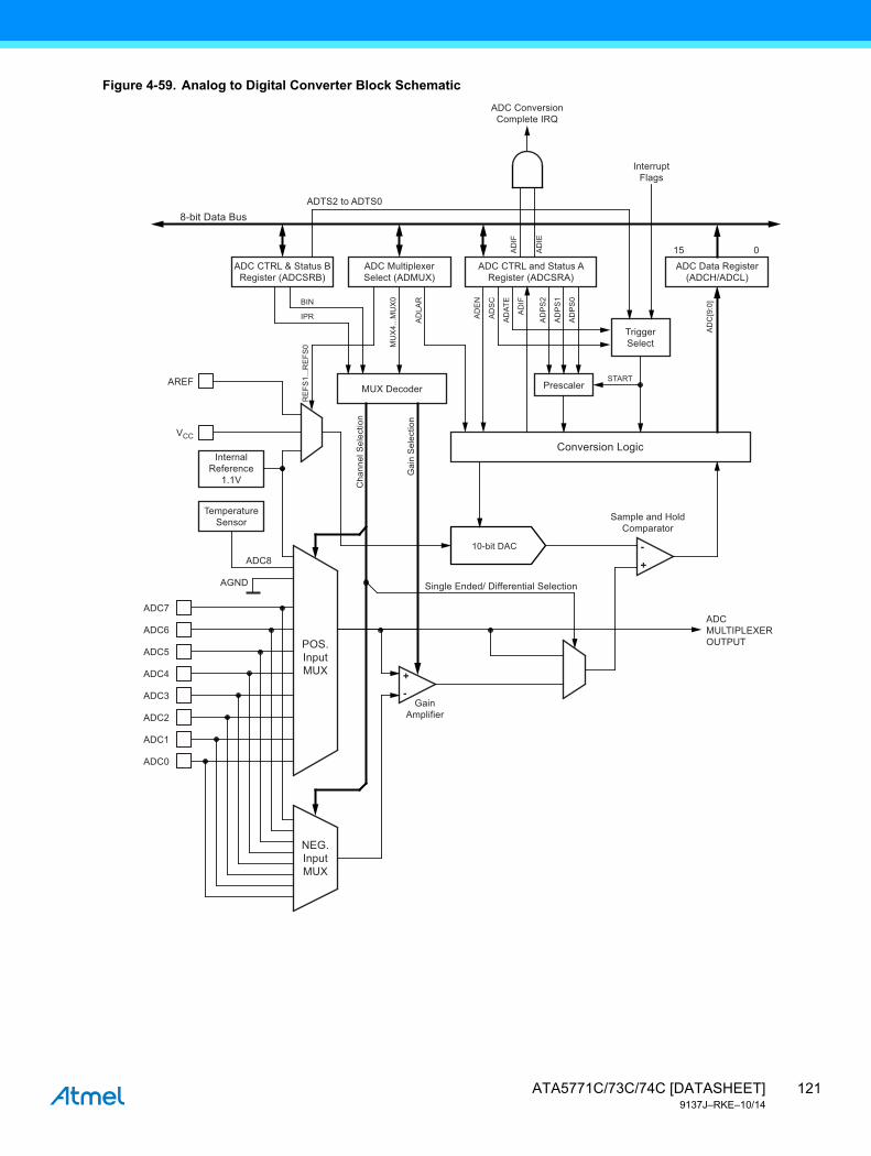
Figure 4-59. Analog to Digital Converter Block Schematic
PrescalerSTART
BIN
Single Ended/ Differential Selection
IPR
ADC8-
+
15 0
ADC MultiplexerSelect (ADMUX)
TriggerSelect
MUX Decoder
VCC
ADTS2 to ADTS0
8-bit Data Bus
InterruptFlags
AREF
10-bit DAC
Sample and HoldComparator
GainAmplifier
InternalReference
1.1V
TemperatureSensor
Conversion Logic
ADC CTRL & Status BRegister (ADCSRB)
ADC ConversionComplete IRQ
ADC CTRL and Status ARegister (ADCSRA)
ADC Data Register(ADCH/ADCL)
+-
AD
IF
AD
EN
Cha
nnel
Sel
ectio
n
Gai
n S
elec
tion
AD
SC
MU
X4.
..MU
X0
RE
FS1.
..RE
FS0
AD
LAR
AD
IF
AD
PS
2
AD
PS
1
AD
PS
0
AD
ATE
AD
IE
AD
C[9
:0]
ADCMULTIPLEXEROUTPUT
ADC7
ADC6
ADC5
ADC4
ADC3
ADC2
ADC1
ADC0
AGND
POS.InputMUX
NEG.InputMUX
121ATA5771C/73C/74C [DATASHEET]9137J–RKE–10/14

4.20.3 ADC Operation
The ADC converts an analog input voltage to a 10-bit digital value through successive approximation. The minimum value represents GND and the maximum value represents the reference voltage.The voltage reference for the ADC may be selected by writing to the REFS1..0 bits in ADMUX. The VCC supply, the AREF pin or an internal 1.1V voltage reference may be selected as the ADC voltage reference.
The analog input channel and differential gain are selected by writing to the MUX5..0 bits in ADMUX. Any of the eight ADC input pins ADC7..0 can be selected as single ended inputs to the ADC. For differential measurements all analog inputs next to each other can be selected as a input pair. Every input is also possible to measure with ADC3. These pairs of differential inputs are measured by ADC trough the differential gain amplifier.
If differential channels are selected, the differential gain stage amplifies the voltage difference between the selected input pair by the selected gain factor, 1x or 20x, according to the setting of the MUX0 bit in ADMUX. This amplified value then becomes the analog input to the ADC. If single ended channels are used, the gain amplifier is bypassed altogether.
The offset of the differential channels can be measure by selecting the same input for both negative and positive input. Offset calibration can be done for ADC0, ADC3 and ADC7. When ADC0 or ADC3 or ADC7 is selected as both the positive and negative input to the differential gain amplifier, the remaining offset in the gain stage and conversion circuitry can be measured directly as the result of the conversion. This figure can be subtracted from subsequent conversions with the same gain setting to reduce offset error to below 1 LSB.
The on-chip temperature sensor is selected by writing the code “100010” to the MUX5..0 bits in ADMUX register.
The ADC is enabled by setting the ADC Enable bit, ADEN in ADCSRA. Voltage reference and input channel selections will not go into effect until ADEN is set. The ADC does not consume power when ADEN is cleared, so it is recommended to switch off the ADC before entering power saving sleep modes.
The ADC generates a 10-bit result which is presented in the ADC data registers, ADCH and ADCL. By default, the result is presented right adjusted, but can optionally be presented left adjusted by setting the ADLAR bit in ADCSRB.
If the result is left adjusted and no more than 8-bit precision is required, it is sufficient to read ADCH. Otherwise, ADCL must be read first, then ADCH, to ensure that the content of the data registers belongs to the same conversion. Once ADCL is read, ADC access to data registers is blocked. This means that if ADCL has been read, and a conversion completes before ADCH is read, neither register is updated and the result from the conversion is lost. When ADCH is read, ADC access to the ADCH and ADCL registers is re-enabled.
The ADC has its own interrupt which can be triggered when a conversion completes. When ADC access to the data registers is prohibited between reading of ADCH and ADCL, the interrupt will trigger even if the result is lost.
4.20.4 Starting a Conversion
A single conversion is started by writing a logical one to the ADC start conversion bit, ADSC. This bit stays high as long as the conversion is in progress and will be cleared by hardware when the conversion is completed. If a different data channel is selected while a conversion is in progress, the ADC will finish the current conversion before performing the channel change.
Alternatively, a conversion can be triggered automatically by various sources. Auto triggering is enabled by setting the ADC auto trigger enable bit, ADATE in ADCSRA. The trigger source is selected by setting the ADC trigger select bits, ADTS in ADCSRB (see description of the ADTS bits for a list of the trigger sources). When a positive edge occurs on the selected trigger signal, the ADC prescaler is reset and a conversion is started. This provides a method of starting conversions at fixed intervals. If the trigger signal still is set when the conversion completes, a new conversion will not be started. If another positive edge occurs on the trigger signal during conversion, the edge will be ignored. Note that an interrupt flag will be set even if the specific interrupt is disabled or the global interrupt enable bit in SREG is cleared. A conversion can thus be triggered without causing an interrupt. However, the interrupt flag must be cleared in order to trigger a new conversion at the next interrupt event.
ATA5771C/73C/74C [DATASHEET]9137J–RKE–10/14
122
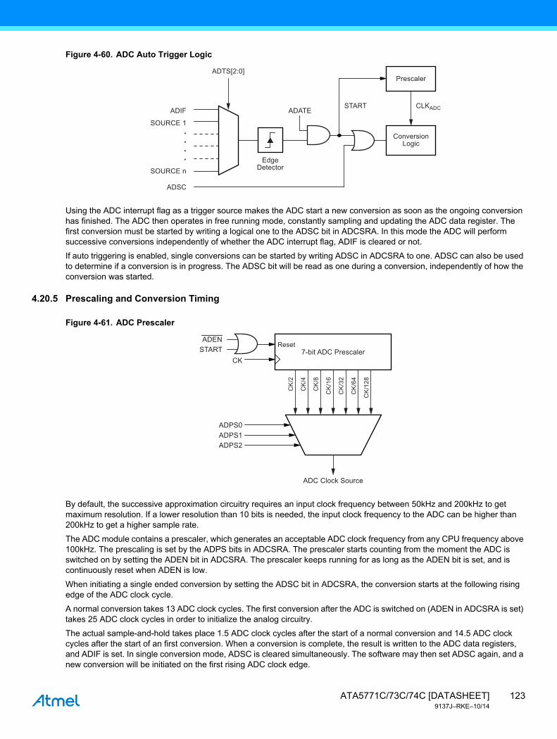
Figure 4-60. ADC Auto Trigger Logic
Using the ADC interrupt flag as a trigger source makes the ADC start a new conversion as soon as the ongoing conversion has finished. The ADC then operates in free running mode, constantly sampling and updating the ADC data register. The first conversion must be started by writing a logical one to the ADSC bit in ADCSRA. In this mode the ADC will perform successive conversions independently of whether the ADC interrupt flag, ADIF is cleared or not.
If auto triggering is enabled, single conversions can be started by writing ADSC in ADCSRA to one. ADSC can also be used to determine if a conversion is in progress. The ADSC bit will be read as one during a conversion, independently of how the conversion was started.
4.20.5 Prescaling and Conversion Timing
Figure 4-61. ADC Prescaler
By default, the successive approximation circuitry requires an input clock frequency between 50kHz and 200kHz to get maximum resolution. If a lower resolution than 10 bits is needed, the input clock frequency to the ADC can be higher than 200kHz to get a higher sample rate.
The ADC module contains a prescaler, which generates an acceptable ADC clock frequency from any CPU frequency above 100kHz. The prescaling is set by the ADPS bits in ADCSRA. The prescaler starts counting from the moment the ADC is switched on by setting the ADEN bit in ADCSRA. The prescaler keeps running for as long as the ADEN bit is set, and is continuously reset when ADEN is low.
When initiating a single ended conversion by setting the ADSC bit in ADCSRA, the conversion starts at the following rising edge of the ADC clock cycle.
A normal conversion takes 13 ADC clock cycles. The first conversion after the ADC is switched on (ADEN in ADCSRA is set) takes 25 ADC clock cycles in order to initialize the analog circuitry.
The actual sample-and-hold takes place 1.5 ADC clock cycles after the start of a normal conversion and 14.5 ADC clock cycles after the start of an first conversion. When a conversion is complete, the result is written to the ADC data registers, and ADIF is set. In single conversion mode, ADSC is cleared simultaneously. The software may then set ADSC again, and a new conversion will be initiated on the first rising ADC clock edge.
EdgeDetector
ConversionLogic
Prescaler
ADIF
ADSC
ADATESTART CLKADC
ADTS[2:0]
.
.
.
.
SOURCE 1
SOURCE n
7-bit ADC Prescaler
ADC Clock Source
ADENSTART
CK
ADPS0ADPS1ADPS2
Reset
CK
/2
CK
/4
CK
/8
CK
/16
CK
/32
CK
/64
CK
/128
123ATA5771C/73C/74C [DATASHEET]9137J–RKE–10/14

When auto triggering is used, the prescaler is reset when the trigger event occurs. This assures a fixed delay from the trigger event to the start of conversion. In this mode, the sample-and-hold takes place two ADC clock cycles after the rising edge on the trigger source signal. Three additional CPU clock cycles are used for synchronization logic.
In free running mode, a new conversion will be started immediately after the conversion completes, while ADSC remains high. For a summary of conversion times, see Table 4-49 on page 125.
Figure 4-62. ADC Timing Diagram, First Conversion (Single Conversion Mode)
Figure 4-63. ADC Timing Diagram, Single Conversion
1 2 12 13 14 15 16 17 18 19 20 21 22 23 24 25 1 2 3Cycle Number
First Conversion
Sign and MSB of Result
LSB of Result
NextConversion
MUX and REFSUpdate
ConversionComplete MUX and REFS
Update
ADC Clock
ADEN
ADSC
ADIF
ADCH
ADCL
Sample and Hold
1 2 3 4 5 6 7 8 9 10 11 12 13 1 2 3Cycle Number
One Conversion
Sign and MSB of Result
LSB of Result
Next Conversion
MUX and REFSUpdate
ConversionComplete MUX and REFS
Update
ADC Clock
ADSC
ADIF
ADCH
ADCL
Sample and Hold
ATA5771C/73C/74C [DATASHEET]9137J–RKE–10/14
124

Figure 4-64. ADC Timing Diagram, Auto Triggered Conversion
Figure 4-65. ADC Timing Diagram, Free Running Conversion
Table 4-49. ADC Conversion Time
ConditionSample and Hold (Cycles from Start of
Conversion) Conversion Time (Cycles)
First conversion 14.5 25
Normal conversions 1.5 13
Auto triggered conversions 2 13.5
1 2 3 4 5 6 7 8 9 10 11 12 13 1 2Cycle Number
One Conversion
Sign and MSB of Result
LSB of Result
Next Conversion
MUX and REFSUpdate
PrescalerReset
PrescalerReset
ConversionComplete
ADC Clock
TriggerSource
ADIF
ADATE
ADCH
ADCL
Sample and Hold
11 12 13 1 2 3 4Cycle Number
One Conversion
Sign and MSB of Result
LSB of Result
Next Conversion
MUX and REFSUpdate
ConversionComplete
ADC Clock
ADSC
ADIF
ADCH
ADCL
Sample and Hold
125ATA5771C/73C/74C [DATASHEET]9137J–RKE–10/14

4.20.6 Changing Channel or Reference Selection
The MUX5:0 and REFS1:0 bits in the ADMUX register are single buffered through a temporary register to which the CPU has random access. This ensures that the channels and reference selection only takes place at a safe point during the conversion. The channel and reference selection is continuously updated until a conversion is started. Once the conversion starts, the channel and reference selection is locked to ensure a sufficient sampling time for the ADC. Continuous updating resumes in the last ADC clock cycle before the conversion completes (ADIF in ADCSRA is set). Note that the conversion starts on the following rising ADC clock edge after ADSC is written. The user is thus advised not to write new channel or reference selection values to ADMUX until one ADC clock cycle after ADSC is written.
If auto triggering is used, the exact time of the triggering event can be indeterministic. Special care must be taken when updating the ADMUX register, in order to control which conversion will be affected by the new settings.
If both ADATE and ADEN is written to one, an interrupt event can occur at any time. If the ADMUX register is changed in this period, the user cannot tell if the next conversion is based on the old or the new settings. ADMUX can be safely updated in the following ways:
a. When ADATE or ADEN is cleared.
b. During conversion, minimum one ADC clock cycle after the trigger event.
c. After a conversion, before the Interrupt Flag used as trigger source is cleared.
When updating ADMUX in one of these conditions, the new settings will affect the next ADC conversion.
4.20.6.1 ADC Input Channels
When changing channel selections, the user should observe the following guidelines to ensure that the correct channel is selected:
In single conversion mode, always select the channel before starting the conversion. The channel selection may be changed one ADC clock cycle after writing one to ADSC. However, the simplest method is to wait for the conversion to complete before changing the channel selection.
In free running mode, always select the channel before starting the first conversion. The channel selection may be changed one ADC clock cycle after writing one to ADSC. However, the simplest method is to wait for the first conversion to complete, and then change the channel selection. Since the next conversion has already started automatically, the next result will reflect the previous channel selection. Subsequent conversions will reflect the new channel selection.
4.20.6.2 ADC Voltage Reference
The reference voltage for the ADC (VREF) indicates the conversion range for the ADC. Single ended channels that exceed VREF will result in codes close to 0x3FF. VREF can be selected as either VCC, or internal 1.1V reference, or external AREF pin. The first ADC conversion result after switching reference voltage source may be inaccurate, and the user is advised to discard this result.
4.20.7 ADC Noise Canceler
The ADC features a noise canceler that enables conversion during sleep mode to reduce noise induced from the CPU core and other I/O peripherals. The noise canceler can be used with ADC Noise Reduction and Idle mode. To make use of this feature, the following procedure should be used:
1. Make sure that the ADC is enabled and is not busy converting. Single conversion mode must be selected and the ADC conversion complete interrupt must be enabled.
2. Enter ADC noise reduction mode (or Idle mode). The ADC will start a conversion once the CPU has been halted.
3. If no other interrupts occur before the ADC conversion completes, the ADC interrupt will wake up the CPU and execute the ADC conversion complete interrupt routine. If another interrupt wakes up the CPU before the ADC conversion is complete, that interrupt will be executed, and an ADC conversion complete interrupt request will be generated when the ADC conversion completes. The CPU will remain in active mode until a new sleep command is executed.
Note that the ADC will not be automatically turned off when entering other sleep modes than Idle mode and ADC noise reduction mode. The user is advised to write zero to ADEN before entering such sleep modes to avoid excessive power consumption.
ATA5771C/73C/74C [DATASHEET]9137J–RKE–10/14
126
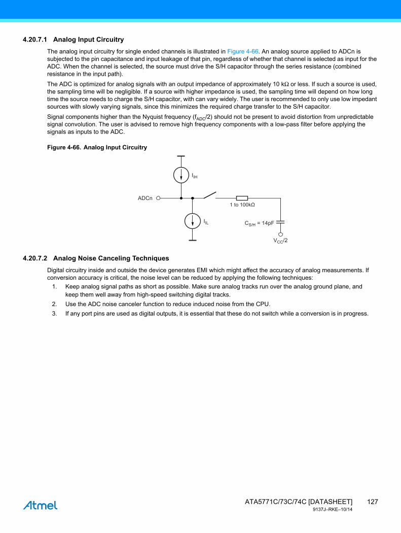
4.20.7.1 Analog Input Circuitry
The analog input circuitry for single ended channels is illustrated in Figure 4-66. An analog source applied to ADCn is subjected to the pin capacitance and input leakage of that pin, regardless of whether that channel is selected as input for the ADC. When the channel is selected, the source must drive the S/H capacitor through the series resistance (combined resistance in the input path).
The ADC is optimized for analog signals with an output impedance of approximately 10 kΩ or less. If such a source is used, the sampling time will be negligible. If a source with higher impedance is used, the sampling time will depend on how long time the source needs to charge the S/H capacitor, with can vary widely. The user is recommended to only use low impedant sources with slowly varying signals, since this minimizes the required charge transfer to the S/H capacitor.
Signal components higher than the Nyquist frequency (fADC/2) should not be present to avoid distortion from unpredictable signal convolution. The user is advised to remove high frequency components with a low-pass filter before applying the signals as inputs to the ADC.
Figure 4-66. Analog Input Circuitry
4.20.7.2 Analog Noise Canceling Techniques
Digital circuitry inside and outside the device generates EMI which might affect the accuracy of analog measurements. If conversion accuracy is critical, the noise level can be reduced by applying the following techniques:
1. Keep analog signal paths as short as possible. Make sure analog tracks run over the analog ground plane, and keep them well away from high-speed switching digital tracks.
2. Use the ADC noise canceler function to reduce induced noise from the CPU.
3. If any port pins are used as digital outputs, it is essential that these do not switch while a conversion is in progress.
IIL
VCC/2
CS/H = 14pF
IIH
ADCn1 to 100kΩ
127ATA5771C/73C/74C [DATASHEET]9137J–RKE–10/14

4.20.7.3 ADC Accuracy Definitions
An n-bit single-ended ADC converts a voltage linearly between GND and VREF in 2n steps (LSBs). The lowest code is read as 0, and the highest code is read as 2n-1.
Several parameters describe the deviation from the ideal behavior:
● Offset: The deviation of the first transition (0x000 to 0x001) compared to the ideal transition (at 0.5 LSB). Ideal value: 0 LSB.
Figure 4-67. Offset Error
● Gain Error: After adjusting for offset, the Gain Error is found as the deviation of the last transition (0x3FE to 0x3FF) compared to the ideal transition (at 1.5 LSB below maximum). Ideal value: 0 LSB
Figure 4-68. Gain Error
OffsetError
Output Code
Ideal ADC
Actual ADC
VREF Input Voltage
Output Code
Ideal ADC
Actual ADC
VREF Input Voltage
GainError
ATA5771C/73C/74C [DATASHEET]9137J–RKE–10/14
128

● Integral Non-linearity (INL): After adjusting for offset and gain error, the INL is the maximum deviation of an actual transition compared to an ideal transition for any code. Ideal value: 0 LSB.
Figure 4-69. Integral Non-linearity (INL)
● Differential Non-linearity (DNL): The maximum deviation of the actual code width (the interval between two adjacent transitions) from the ideal code width (1 LSB). Ideal value: 0 LSB.
Figure 4-70. Differential Non-linearity (DNL)
● Quantization Error: Due to the quantization of the input voltage into a finite number of codes, a range of input voltages (1 LSB wide) will code to the same value. Always ±0.5 LSB.
● Absolute Accuracy: The maximum deviation of an actual (unadjusted) transition compared to an ideal transition for any code. This is the compound effect of offset, gain error, differential error, non-linearity, and quantization error. Ideal value: ±0.5 LSB.
Output Code
Ideal ADCINL
Actual ADC
VREF Input Voltage
Output Code
0x3FF
0x000
0
1 LSB
DNL
VREF Input Voltage
129ATA5771C/73C/74C [DATASHEET]9137J–RKE–10/14

4.20.8 ADC Conversion Result
After the conversion is complete (ADIF is high), the conversion result can be found in the ADC Result Registers (ADCL, ADCH). The form of the conversion result depends on the type of the conversion as there are three types of conversions: single ended conversion, unipolar differential conversion and bipolar differential conversion.
4.20.8.1 Single Ended Conversion
For single ended conversion, the result is
where VIN is the voltage on the selected input pin and VREF the selected voltage reference (see Table 4-51 on page 131 and Table 4-52 on page 132). 0x000 represents analog ground, and 0x3FF represents the selected reference voltage minus one LSB. The result is presented in one-sided form, from 0x3FF to 0x000.
4.20.8.2 Unipolar Differential Conversion
If differential channels and an unipolar input mode are used, the result is
where VPOS is the voltage on the positive input pin, VNEG the voltage on the negative input pin, and VREF the selected voltage reference. The voltage of the positive pin must always be larger than the voltage of the negative pin or otherwise the voltage difference is saturated to zero. The result is presented in one-sided form, from 0x000 (0d) through 0x3FF (+1023d). The GAIN is either 1x or 20x.
4.20.8.3 Bipolar Differential Conversion
If differential channels and a bipolar input mode are used, the result is
where VPOS is the voltage on the positive input pin, VNEG the voltage on the negative input pin, and VREF the selected voltage reference. The result is presented in two’s complement form, from 0x200 (-512d) through 0x1FF (+511d). The GAIN is either 1x or 20x. Note that if the user wants to perform a quick polarity check of the result, it is sufficient to read the MSB of the result (ADC9 in ADCH). If the bit is one, the result is negative, and if this bit is zero, the result is positive.
As default the ADC converter operates in the unipolar input mode, but the bipolar input mode can be selected by writing the BIN bit in the ADCSRB to one. In the bipolar input mode two-sided voltage differences are allowed and thus the voltage on the negative input pin can also be larger than the voltage on the positive input pin.
4.20.9 Temperature Measurement
The temperature measurement is based on an on-chip temperature sensor that is coupled to a single ended ADC8 channel. Selecting the ADC8 channel by writing the MUX5:0 bits in ADMUX register to “100010” enables the temperature sensor. The internal 1.1V reference must also be selected for the ADC reference source in the temperature sensor measurement. When the temperature sensor is enabled, the ADC converter can be used in single conversion mode to measure the voltage over the temperature sensor. The measured voltage has a linear relationship to the temperature as described in Table 4-50. The voltage sensitivity is approximately 1mV/°C and the accuracy of the temperature measurement is ±10°C after offset calibration. Bandgap is always calibrated and its accuracy is only guaranteed between 1.0V and 1.2V.
ADCVIN 1024⋅VREF
-------------------------=
ADCVPOS VNEG–( ) 1024⋅
VREF------------------------------------------------------- GAIN⋅=
ADCVPOS VNEG–( ) 512⋅
VREF---------------------------------------------------- GAIN⋅=
Table 4-50. Temperature versus Sensor Output Voltage (Typical Case)
Temperature / °C –40°C +25°C +85°C +125°C
Voltage / mV 243mV 314mv 380mV 424mV
ATA5771C/73C/74C [DATASHEET]9137J–RKE–10/14
130

The values described in Table 4-50 on page 130 are typical values. However, due to the process variation the temperature sensor output voltage varies from one chip to another. To be capable of achieving more accurate results the temperature measurement can be calibrated in the application software. The software calibration requires that a calibration value is measured and stored in a register or EEPROM for each chip, as a part of the production test. The software calibration can be done utilizing the formula:
T = {[(ADCH << 8) | ADCL] - TOS} / k
where ADCn are the ADC data registers, k is a fixed coefficient and TOS is the temperature sensor offset value determined and stored into EEPROM as a part of the production test.To obtain best accuracy the coefficient k should be measured using two temperature calibrations. Using offset calibration, set k = 1.0, where k = (1024 × 1.07mV/°C)/1.1V~1.0 [1/°C].
4.20.10 Register Description
4.20.10.1 ADMUX – ADC Multiplexer Selection Register
• Bit 7:6 – REFS1:REFS0: Reference Selection Bits
These bits select the voltage reference for the ADC, as shown in Table 4-51 on page 131. If these bits are changed during a conversion, the change will not go in effect until this conversion is complete (ADIF in ADCSR is set).
Special care should be taken when changing differential channels. Once a differential channel has been selected, the stage may take as much as 25 ADC clock cycles to stabilize to the new value. Thus conversions should not be started within the first 13 clock cycles after selecting a new differential channel. Alternatively, conversion results obtained within this period should be discarded.
The same settling time should be observed for the first differential conversion after changing ADC reference (by changing the REFS1:0 bits in ADMUX).
If channels where differential gain is used ie. the gainstage, using VCC or an optional external AREF higher than (VCC – 1V) is not recommended, as this will affect ADC accuracy. It is not allowed to connect internal voltage reference to AREF pin, if an external voltage is being applied to it already. Internal voltage reference is connected AREF pin when REFS1:0 is set to value ‘11’.
• Bits 5:0 – MUX5:0: Analog Channel and Gain Selection Bits
The value of these bits selects which combination of analog inputs are connected to the ADC. In case of differential input, gain selection is also made with these bits. Selections on Table 4-52 show values for single ended channels and where the differential channels as well as the offset calibration selections are located. Selecting the single-ended channel ADC8 enables the temperature measurement. See Table 4-52 for details. If these bits are changed during a conversion, the change will not go into effect until this conversion is complete (ADIF in ADCSRA is set).
Bit 7 6 5 4 3 2 1 0
0x07 (0x27) REFS1 REFS0 MUX5 MUX4 MUX3 MUX2 MUX1 MUX0 ADMUX
Read/Write R/W R/W R/W R/W R/W R/W R/W R/W
Initial Value 0 0 0 0 0 0 0 0
Table 4-51. Voltage Reference Selections for ADC
REFS1 REFS0 Voltage Reference Selection
0 0 VCC used as analog reference, disconnected from PA0 (AREF)
0 1 External voltage reference at PA0 (AREF) pin, internal voltage reference turned off
1 0 Internal 1.1V voltage reference
1 1 Reserved
131ATA5771C/73C/74C [DATASHEET]9137J–RKE–10/14
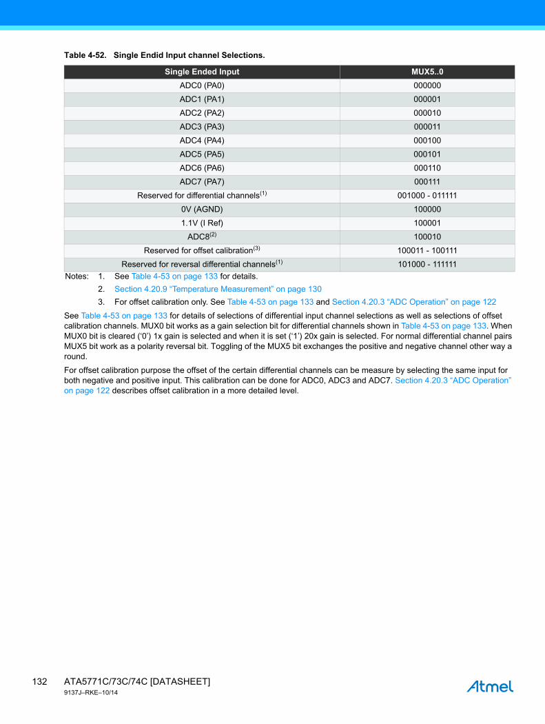
See Table 4-53 on page 133 for details of selections of differential input channel selections as well as selections of offset calibration channels. MUX0 bit works as a gain selection bit for differential channels shown in Table 4-53 on page 133. When MUX0 bit is cleared (‘0’) 1x gain is selected and when it is set (‘1’) 20x gain is selected. For normal differential channel pairs MUX5 bit work as a polarity reversal bit. Toggling of the MUX5 bit exchanges the positive and negative channel other way a round.
For offset calibration purpose the offset of the certain differential channels can be measure by selecting the same input for both negative and positive input. This calibration can be done for ADC0, ADC3 and ADC7. Section 4.20.3 “ADC Operation” on page 122 describes offset calibration in a more detailed level.
Table 4-52. Single Endid Input channel Selections.
Single Ended Input MUX5..0
ADC0 (PA0) 000000
ADC1 (PA1) 000001
ADC2 (PA2) 000010
ADC3 (PA3) 000011
ADC4 (PA4) 000100
ADC5 (PA5) 000101
ADC6 (PA6) 000110
ADC7 (PA7) 000111
Reserved for differential channels(1) 001000 - 011111
0V (AGND) 100000
1.1V (I Ref) 100001
ADC8(2) 100010
Reserved for offset calibration(3) 100011 - 100111
Reserved for reversal differential channels(1) 101000 - 111111
Notes: 1. See Table 4-53 on page 133 for details.
2. Section 4.20.9 “Temperature Measurement” on page 130
3. For offset calibration only. See Table 4-53 on page 133 and Section 4.20.3 “ADC Operation” on page 122
ATA5771C/73C/74C [DATASHEET]9137J–RKE–10/14
132

Table 4-53. Differential Input Channel Selections.
Positive Differential Input Negative Differential Input
MUX5..0
Gain 1x Gain 20x
ADC0 (PA0)
ADC0 (PA0)(1) N/A 100011
ADC1 (PA1) 001000 001001
ADC3 (PA3) 001010 001011
ADC1 (PA1)
ADC0 (PA0) 101000 101001
ADC2 (PA2) 001100 001101
ADC3 (PA3) 001110 001111
ADC2 (PA2)ADC1 (PA1) 101100 101101
ADC3 (PA3) 010000 010001
ADC3 (PA3)
ADC0 (PA0) 101010 101011
ADC1 (PA1) 101110 101111
ADC2 (PA2) 110000 110001
ADC3 (PA3)(1) 100100 100101
ADC4 (PA4 010010 010011
ADC5 (PA5) 010100 010101
ADC6 (PA6) 010110 010111
ADC7 (PA7) 011000 011001
ADC4 (PA4ADC3 (PA3) 110010 110011
ADC5 (PA5) 011010 011011
ADC5 (PA5)
ADC3 (PA3) 110100 110101
ADC4 (PA4) 111010 111011
ADC6 (PA6) 011100 011101
ADC6 (PA6)
ADC3 (PA3) 110110 110111
ADC5 (PA5) 111100 111101
ADC7 (PA7) 011110 011111
ADC7 (PA7)
ADC3 (PA3) 111000 111001
ADC6 (PA6) 111110 111111
ADC7 (PA7)(1) 100110 100111
Notes: 1. For offset calibration only. See Section 4.20.3 “ADC Operation” on page 122.
133ATA5771C/73C/74C [DATASHEET]9137J–RKE–10/14

4.20.10.2 ADCSRA – ADC Control and Status Register A
• Bit 7 – ADEN: ADC Enable
Writing this bit to one enables the ADC. By writing it to zero, the ADC is turned off. Turning the ADC off while a conversion is in progress, will terminate this conversion.
• Bit 6 – ADSC: ADC Start Conversion
In single conversion mode, write this bit to one to start each conversion. In free running mode, write this bit to one to start the first conversion. The first conversion after ADSC has been written after the ADC has been enabled, or if ADSC is written at the same time as the ADC is enabled, will take 25 ADC clock cycles instead of the normal 13. This first conversion performs initialization of the ADC.
ADSC will read as one as long as a conversion is in progress. When the conversion is complete, it returns to zero. Writing zero to this bit has no effect.
• Bit 5 – ADATE: ADC Auto Trigger Enable
When this bit is written to one, auto triggering of the ADC is enabled. The ADC will start a conversion on a positive edge of the selected trigger signal. The trigger source is selected by setting the ADC trigger select bits, ADTS in ADCSRB.
• Bit 4 – ADIF: ADC Interrupt Flag
This bit is set when an ADC conversion completes and the data registers are updated. The ADC conversion complete Interrupt is executed if the ADIE bit and the I-bit in SREG are set. ADIF is cleared by hardware when executing the corresponding interrupt handling vector. Alternatively, ADIF is cleared by writing a logical one to the flag. Beware that if doing a read-modify-write on ADCSRA, a pending interrupt can be disabled. This also applies if the SBI instruction is used.
• Bit 3 – ADIE: ADC Interrupt Enable
When this bit is written to one and the I-bit in SREG is set, the ADC conversion complete Interrupt is activated.
• Bits 2:0 – ADPS2:0: ADC Prescaler Select Bits
These bits determine the division factor between the system clock frequency and the input clock to the ADC.
Bit 7 6 5 4 3 2 1 0
0x06 (0x26) ADEN ADSC ADATE ADIF ADIE ADPS2 ADPS1 ADPS0 ADCSRA
Read/Write R/W R/W R/W R/W R/W R/W R/W R/W
Initial Value 0 0 0 0 0 0 0 0
Table 4-54. ADC Prescaler Selections
ADPS2 ADPS1 ADPS0 Division Factor
0 0 0 2
0 0 1 2
0 1 0 4
0 1 1 8
1 0 0 16
1 0 1 32
1 1 0 64
1 1 1 128
ATA5771C/73C/74C [DATASHEET]9137J–RKE–10/14
134

4.20.10.3 ADCL and ADCH – ADC Data Register
ADLAR = 0
ADLAR = 1
When an ADC conversion is complete, the result is found in these two registers.
When ADCL is read, the ADC data register is not updated until ADCH is read. Consequently, if the result is left adjusted and no more than 8-bit precision is required, it is sufficient to read ADCH. Otherwise, ADCL must be read first, then ADCH.
The ADLAR bit in ADCSRB, and the MUXn bits in ADMUX affect the way the result is read from the registers. If ADLAR is set, the result is left adjusted. If ADLAR is cleared (default), the result is right adjusted.
• ADC9:0: ADC Conversion Result
These bits represent the result from the conversion, as detailed in Section 4.20.8 “ADC Conversion Result” on page 130.
4.20.10.4 ADCSRB – ADC Control and Status Register B
• Bits 7 – BIN: Bipolar Input Mode
The gain stage is working in the unipolar mode as default, but the bipolar mode can be selected by writing the BIN bit in the ADCSRB register. In the unipolar mode only one-sided conversions are supported and the voltage on the positive input must always be larger than the voltage on the negative input. Otherwise the result is saturated to the voltage reference. In the bipolar mode two-sided conversions are supported and the result is represented in the two’s complement form. In the unipolar mode the resolution is 10 bits and the bipolar mode the resolution is 9 bits + 1 sign bit.
• Bit 6 – ACME: Analog Comparator Multiplexer Enable
See Section 4.20.10.4 “ADCSRB – ADC Control and Status Register B” on page 135.
• Bit 5 – Res: Reserved Bit
This bit is reserved bit in the Atmel® ATtiny44V and will always read as what was wrote there.
Bit 15 14 13 12 11 10 9 8
0x05 (0x25) – – – – – – ADC9 ADC8 ADCH
0x04 (0x24) ADC7 ADC6 ADC5 ADC4 ADC3 ADC2 ADC1 ADC0 ADCL
7 6 5 4 3 2 1 0
Read/Write R R R R R R R R
R R R R R R R R
Initial Value 0 0 0 0 0 0 0 0
0 0 0 0 0 0 0 0
Bit 15 14 13 12 11 10 9 8
0x05 (0x25) ADC9 ADC8 ADC7 ADC6 ADC5 ADC4 ADC3 ADC2 ADCH
0x04 (0x24) ADC1 ADC0 – – – – – – ADCL
7 6 5 4 3 2 1 0
Read/Write R R R R R R R R
R R R R R R R R
Initial Value 0 0 0 0 0 0 0 0
0 0 0 0 0 0 0 0
Bit 7 6 5 4 3 2 1 0
0x03 (0x23) BIN ACME – ADLAR – ADTS2 ADTS1 ADTS0 ADCSRB
Read/Write R/W R/W R/W R/W R/W R/W R/W R/W
Initial Value 0 0 0 0 0 0 0 0
135ATA5771C/73C/74C [DATASHEET]9137J–RKE–10/14

• Bit 4 – ADLAR: ADC Left Adjust Result
The ADLAR bit affects the presentation of the ADC conversion result in the ADC data register. Write one to ADLAR to left adjust the result. Otherwise, the result is right adjusted. Changing the ADLAR bit will affect the ADC data register immediately, regardless of any ongoing conversions. For a complete description of this bit, see Section 4.20.10.3 “ADCL and ADCH – ADC Data Register” on page 135.
• Bit 3 – Res: Reserved Bit
This bit is reserved bit in the ATtiny44V and will always read as what was wrote there.
• Bits 2:0 – ADTS2:0: ADC Auto Trigger Source
If ADATE in ADCSRA is written to one, the value of these bits selects which source will trigger an ADC conversion. If ADATE is cleared, the ADTS2:0 settings will have no effect. A conversion will be triggered by the rising edge of the selected Interrupt Flag. Note that switching from a trigger source that is cleared to a trigger source that is set, will generate a positive edge on the trigger signal. If ADEN in ADCSRA is set, this will start a conversion. Switching to free running mode (ADTS[2:0]=0) will not cause a trigger event, even if the ADC interrupt flag is set.
4.20.10.5 DIDR0 – Digital Input Disable Register 0
• Bits 7..0 – ADC7D..ADC0D: ADC7..0 Digital Input Disable
When this bit is written logic one, the digital input buffer on the corresponding ADC pin is disabled. The corresponding PIN register bit will always read as zero when this bit is set. When an analog signal is applied to the ADC7..0 pin and the digital input from this pin is not needed, this bit should be written logic one to reduce power consumption in the digital input buffer.
Table 4-55. ADC Auto Trigger Source Selections
ADTS2 ADTS1 ADTS0 Trigger Source
0 0 0 Free running mode
0 0 1 Analog comparator
0 1 0 External interrupt request 0
0 1 1 Timer/Counter0 compare match A
1 0 0 Timer/Counter0 overflow
1 0 1 Timer/Counter1 compare match B
1 1 0 Timer/Counter1 overflow
1 1 1 Timer/Counter1 capture event
Bit 7 6 5 4 3 2 1 0
0x01 (0x21) ADC7D ADC6D ADC5D ADC4D ADC3D ADC2D ADC1D ADC0D DIDR0
Read/Write R/W R/W R/W R/W R/W R/W R/W R/W
Initial Value 0 0 0 0 0 0 0 0
ATA5771C/73C/74C [DATASHEET]9137J–RKE–10/14
136

4.21 debugWIRE On-chip Debug System
4.21.1 Features
● Complete program flow control
● Emulates all on-chip functions, both digital and analog, except RESET pin
● Real-time operation
● Symbolic debugging support (both at C and assembler source level, or for other HLLs)
● Unlimited number of program break points (using software break points)
● Non-intrusive operation
● Electrical characteristics identical to real device
● Automatic configuration system
● High-speed operation
● Programming of non-volatile memories
4.21.2 Overview
The debugWIRE On-chip debug system uses a one-wire, bi-directional interface to control the program flow, execute Atmel® AVR® instructions in the CPU and to program the different non-volatile memories.
4.21.3 Physical Interface
When the debugWIRE Enable (DWEN) Fuse is programmed and Lock bits are unprogrammed, the debugWIRE system within the target device is activated. The RESET port pin is configured as a wire-AND (open-drain) bi-directional I/O pin with pull-up enabled and becomes the communication gateway between target and emulator.
Figure 4-71. The debugWIRE Setup
Figure 4-71 shows the schematic of a target MCU, with debugWIRE enabled, and the emulator connector. The system clock is not affected by debugWIRE and will always be the clock source selected by the CKSEL fuses.
When designing a system where debugWIRE will be used, the following observations must be made for correct operation:
● Pull-up resistor on the dW/(RESET) line must be in the range of 10kΩ to 20kΩ. However, the pull-up resistor is optional.
● Connecting the RESET pin directly to VCC will not work.
● Capacitors inserted on the RESET pin must be disconnected when using debugWire.
● All external reset sources must be disconnected.
GND
1.8 - 5.5V
dw
VCC
dw (RESET)
137ATA5771C/73C/74C [DATASHEET]9137J–RKE–10/14

4.21.4 Software Break Points
debugWIRE supports program memory break points by the Atmel® AVR® break instruction. Setting a break point in Atmel AVR Studio® will insert a BREAK instruction in the program memory. The instruction replaced by the BREAK instruction will be stored. When program execution is continued, the stored instruction will be executed before continuing from the program memory. A break can be inserted manually by putting the BREAK instruction in the program.
The flash must be re-programmed each time a break point is changed. This is automatically handled by AVR Studio through the debugWIRE interface. The use of break points will therefore reduce the flash data retention. Devices used for debugging purposes should not be shipped to end customers.
4.21.5 Limitations of debugWIRE
The debugWIRE communication pin (dW) is physically located on the same pin as external reset (RESET). An external reset source is therefore not supported when the debugWIRE is enabled.
The debugWIRE system accurately emulates all I/O functions when running at full speed, i.e., when the program in the CPU is running. When the CPU is stopped, care must be taken while accessing some of the I/O registers via the debugger (AVR Studio). See the debugWIRE documentation for detailed description of the limitations.
A programmed DWEN fuse enables some parts of the clock system to be running in all sleep modes. This will increase the power consumption while in sleep. Thus, the DWEN Fuse should be disabled when debugWire is not used.
4.21.6 Register Description
The following section describes the registers used with the debugWire.
4.21.6.1 DWDR – debugWire Data Register
The DWDR register provides a communication channel from the running program in the MCU to the debugger. This register is only accessible by the debugWIRE and can therefore not be used as a general purpose register in the normal operations.
4.22 Self-Programming the Flash
The device provides a self-programming mechanism for downloading and uploading program code by the MCU itself. The self-programming can use any available data interface and associated protocol to read code and write (program) that code into the program memory.
The program memory is updated in a page by page fashion. Before programming a page with the data stored in the temporary page buffer, the page must be erased. The temporary page buffer is filled one word at a time using SPM and the buffer can be filled either before the page erase command or between a page erase and a page write operation:
Alternative 1, fill the buffer before a page erase
● Fill temporary page buffer
● Perform a page erase
● Perform a page write
Alternative 2, fill the buffer after page erase
● Perform a page erase
● Fill temporary page buffer
● Perform a page write
If only a part of the page needs to be changed, the rest of the page must be stored (for example in the temporary page buffer) before the erase, and then be re-written. When using alternative 1, the boot loader provides an effective read-modify-write feature which allows the user software to first read the page, do the necessary changes, and then write back the modified data. If alternative 2 is used, it is not possible to read the old data while loading since the page is already erased. The temporary page buffer can be accessed in a random sequence. It is essential that the page address used in both the page erase and page write operation is addressing the same page.
Bit 7 6 5 4 3 2 1 0
0x27 (0x47) DWDR[7:0] DWDR
Read/Write R/W R/W R/W R/W R/W R/W R/W R/W
Initial Value 0 0 0 0 0 0 0 0
ATA5771C/73C/74C [DATASHEET]9137J–RKE–10/14
138
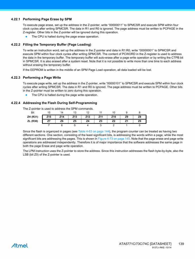
4.22.1 Performing Page Erase by SPM
To execute page erase, set up the address in the Z-pointer, write “00000011” to SPMCSR and execute SPM within four clock cycles after writing SPMCSR. The data in R1 and R0 is ignored. The page address must be written to PCPAGE in the Z-register. Other bits in the Z-pointer will be ignored during this operation.
● The CPU is halted during the page erase operation.
4.22.2 Filling the Temporary Buffer (Page Loading)
To write an instruction word, set up the address in the Z-pointer and data in R1:R0, write “00000001” to SPMCSR and execute SPM within four clock cycles after writing SPMCSR. The content of PCWORD in the Z-register is used to address the data in the temporary buffer. The temporary buffer will auto-erase after a page write operation or by writing the CTPB bit in SPMCSR. It is also erased after a system reset. Note that it is not possible to write more than one time to each address without erasing the temporary buffer.
If the EEPROM is written in the middle of an SPM Page Load operation, all data loaded will be lost.
4.22.3 Performing a Page Write
To execute page write, set up the address in the Z-pointer, write “00000101” to SPMCSR and execute SPM within four clock cycles after writing SPMCSR. The data in R1 and R0 is ignored. The page address must be written to PCPAGE. Other bits in the Z-pointer must be written to zero during this operation.
● The CPU is halted during the page write operation.
4.22.4 Addressing the Flash During Self-Programming
The Z-pointer is used to address the SPM commands.
Since the flash is organized in pages (see Table 4-63 on page 144), the program counter can be treated as having two different sections. One section, consisting of the least significant bits, is addressing the words within a page, while the most significant bits are addressing the pages. This is shown in Figure 4-73 on page 145. Note that the page erase and page write operations are addressed independently. Therefore it is of major importance that the software addresses the same page in both the page Erase and page write operation.
The LPM instruction uses the Z-pointer to store the address. Since this instruction addresses the flash byte-by-byte, also the LSB (bit Z0) of the Z-pointer is used.
Bit 15 14 13 12 11 10 9 8
ZH (R31) Z15 Z14 Z13 Z12 Z11 Z10 Z9 Z8
ZL (R30) Z7 Z6 Z5 Z4 Z3 Z2 Z1 Z0
7 6 5 4 3 2 1 0
139ATA5771C/73C/74C [DATASHEET]9137J–RKE–10/14

Figure 4-72. Addressing the Flash During SPM(1)
Note: The different variables used in Figure 4-72 are listed in Table 4-63 on page 144.
4.22.4.1 EEPROM Write Prevents Writing to SPMCSR
Note that an EEPROM write operation will block all software programming to flash. Reading the fuses and lock bits from software will also be prevented during the EEPROM write operation. It is recommended that the user checks the status bit (EEPE) in the EECR register and verifies that the bit is cleared before writing to the SPMCSR register.
4.22.4.2 Reading the Fuse and Lock Bits from Software
It is possible to read both the fuse and lock bits from software. To read the Lock bits, load the Z-pointer with 0x0001 and set the RFLB and SPMEN bits in SPMCSR. When an LPM instruction is executed within three CPU cycles after the RFLB and SPMEN bits are set in SPMCSR, the value of the Lock bits will be loaded in the destination register. The RFLB and SPMEN bits will auto-clear upon completion of reading the Lock bits or if no LPM instruction is executed within three CPU cycles or no SPM instruction is executed within four CPU cycles. When RFLB and SPMEN are cleared, LPM will work as described in the instruction set manual.
The algorithm for reading the fuse Low byte is similar to the one described above for reading the lock bits. To read the fuse low byte, load the Z-pointer with 0x0000 and set the RFLB and SPMEN bits in SPMCSR. When an LPM instruction is executed within three cycles after the RFLB and SPMEN bits are set in the SPMCSR, the value of the fuse low byte (FLB) will be loaded in the destination register as shown below. See Table 4-61 on page 144 for a detailed description and mapping of the fuse low byte.
Similarly, when reading the fuse high byte, load 0x0003 in the Z-pointer. When an LPM instruction is executed within three cycles after the RFLB and SPMEN bits are set in the SPMCSR, the value of the fuse high byte (FHB) will be loaded in the destination register as shown below. See Table 4-60 on page 143 for detailed description and mapping of the fuse high byte.
Fuse and lock bits that are programmed, will be read as zero. Fuse and lock bits that are unprogrammed, will be read as one.
BIT
PAGEMSBPCMSB
ZPAGEMSBZPCMSB 0115Z-REGISTER
PROGRAMCOUNTER
WORD ADDRESSWITHIN A PAGE
PAGE ADDRESSWITHIN THE FLASH
0
PCWORDPCPAGE
Instruction WordPage
0201
00
PAGEEND
PCWORD[PAGEMSB:0]Page
Program Memory
Bit 7 6 5 4 3 2 1 0
Rd – – – – – – LB2 LB1
Bit 7 6 5 4 3 2 1 0
Rd FLB7 FLB6 FLB5 FLB4 FLB3 FLB2 FLB1 FLB0
Bit 7 6 5 4 3 2 1 0
Rd FHB7 FHB6 FHB5 FHB4 FHB3 FHB2 FHB1 FHB0
ATA5771C/73C/74C [DATASHEET]9137J–RKE–10/14
140
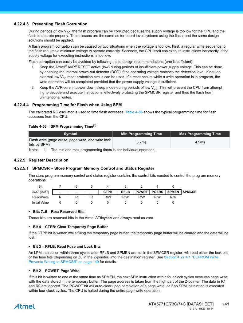
4.22.4.3 Preventing Flash Corruption
During periods of low VCC, the flash program can be corrupted because the supply voltage is too low for the CPU and the flash to operate properly. These issues are the same as for board level systems using the flash, and the same design solutions should be applied.
A flash program corruption can be caused by two situations when the voltage is too low. First, a regular write sequence to the flash requires a minimum voltage to operate correctly. Secondly, the CPU itself can execute instructions incorrectly, if the supply voltage for executing instructions is too low.
Flash corruption can easily be avoided by following these design recommendations (one is sufficient):
1. Keep the Atmel® AVR® RESET active (low) during periods of insufficient power supply voltage. This can be done by enabling the internal brown-out detector (BOD) if the operating voltage matches the detection level. If not, an external low VCC reset protection circuit can be used. If a reset occurs while a write operation is in progress, the write operation will be completed provided that the power supply voltage is sufficient.
2. Keep the AVR core in power-down sleep mode during periods of low VCC. This will prevent the CPU from attempt-ing to decode and execute instructions, effectively protecting the SPMCSR register and thus the flash from unintentional writes.
4.22.4.4 Programming Time for Flash when Using SPM
The calibrated RC oscillator is used to time flash accesses. Table 4-56 shows the typical programming time for flash accesses from the CPU.
4.22.5 Register Description
4.22.5.1 SPMCSR – Store Program Memory Control and Status Register
The store program memory control and status register contains the control bits needed to control the program memory operations.
• Bits 7..5 – Res: Reserved Bits
These bits are reserved bits in the Atmel ATtiny44V and always read as zero.
• Bit 4 – CTPB: Clear Temporary Page Buffer
If the CTPB bit is written while filling the temporary page buffer, the temporary page buffer will be cleared and the data will be lost.
• Bit 3 – RFLB: Read Fuse and Lock Bits
An LPM instruction within three cycles after RFLB and SPMEN are set in the SPMCSR register, will read either the lock bits or the fuse bits (depending on Z0 in the Z-pointer) into the destination register. See Section 4.22.4.1 “EEPROM Write Prevents Writing to SPMCSR” on page 140 for details.
• Bit 2 – PGWRT: Page Write
If this bit is written to one at the same time as SPMEN, the next SPM instruction within four clock cycles executes page write, with the data stored in the temporary buffer. The page address is taken from the high part of the Z-pointer. The data in R1 and R0 are ignored. The PGWRT bit will auto-clear upon completion of a page write, or if no SPM instruction is executed within four clock cycles. The CPU is halted during the entire page write operation.
Table 4-56. SPM Programming Time(1)
Symbol Min Programming Time Max Programming Time
Flash write (page erase, page write, and write lock bits by SPM)
3.7ms 4.5ms
Note: 1. The min and max programming times is per individual operation.
Bit 7 6 5 4 3 2 1 0
0x37 (0x57) – – – CTPB RFLB PGWRT PGERS SPMEN SPMCSR
Read/Write R R R R/W R/W R/W R/W R/W
Initial Value 0 0 0 0 0 0 0 0
141ATA5771C/73C/74C [DATASHEET]9137J–RKE–10/14

• Bit 1 – PGERS: Page Erase
If this bit is written to one at the same time as SPMEN, the next SPM instruction within four clock cycles executes page erase. The page address is taken from the high part of the Z-pointer. The data in R1 and R0 are ignored. The PGERS bit will auto-clear upon completion of a page erase, or if no SPM instruction is executed within four clock cycles. The CPU is halted during the entire page write operation.
• Bit 0 – SPMEN: Store Program Memory Enable
This bit enables the SPM instruction for the next four clock cycles. If written to one together with either CTPB, RFLB, PGWRT, or PGERS, the following SPM instruction will have a special meaning, see description above. If only SPMEN is written, the following SPM instruction will store the value in R1:R0 in the temporary page buffer addressed by the Z-pointer. The LSB of the Z-pointer is ignored. The SPMEN bit will auto-clear upon completion of an SPM instruction, or if no SPM instruction is executed within four clock cycles. During Page Erase and Page Write, the SPMEN bit remains high until the operation is completed.
Writing any other combination than “10001”, “01001”, “00101”, “00011” or “00001” in the lower five bits will have no effect.
4.23 Memory Programming
This section describes the different methods for programming the Atmel® ATtiny44V memories.
4.23.1 Program and Data Memory Lock Bits
The ATtiny44V provides two lock bits which can be left unprogrammed (“1”) or can be programmed (“0”) to obtain the additional security listed in Table 4-58. The lock bits can only be erased to “1” with the chip erase command.
Program memory can be read out via the debugWIRE interface when the DWEN fuse is programmed, even if the lock bits are set. Thus, when lock bit security is required, should always debugWIRE be disabled by clearing the DWEN fuse.
Note: 1. “1” means unprogrammed, “0” means programmed
Table 4-57. Lock Bit Byte(1)
Lock Bit Byte Bit No Description Default Value
7 – 1 (unprogrammed)
6 – 1 (unprogrammed)
5 – 1 (unprogrammed)
4 – 1 (unprogrammed)
3 – 1 (unprogrammed)
2 – 1 (unprogrammed)
LB2 1 Lock bit 1 (unprogrammed)
LB1 0 Lock bit 1 (unprogrammed)
Table 4-58. Lock Bit Protection Modes(1)(2)
Memory Lock Bits Protection Type
LB Mode LB2 LB1
1 1 1 No memory lock features enabled.
2 1 0Further programming of the flash and EEPROM is disabled in high-voltage and serial programming mode. The Fuse bits are locked in both serial and high-voltage programming mode(1). debugWire is disabled.
3 0 0Further programming and verification of the flash and EEPROM is disabled in high-voltage and serial Programming mode. The fuse bits are locked in both serial and high-voltage programming mode1). debugWire is disabled.
Notes: 1. Program the fuse bits before programming the LB1 and LB2.
2. “1” means unprogrammed, “0” means programmed
ATA5771C/73C/74C [DATASHEET]9137J–RKE–10/14
142

4.23.2 Fuse Bytes
The Atmel® ATtiny44V has three Fuse bytes. Table 4-60 to Table 4-61 on page 144 describe briefly the functionality of all the fuses and how they are mapped into the Fuse bytes. Note that the fuses are read as logical zero, “0”, if they are programmed.
Table 4-59. Fuse Extended Byte
Fuse High Byte Bit No Description Default Value
7 - 1 (unprogrammed)
6 - 1 (unprogrammed)
5 - 1 (unprogrammed)
4 - 1 (unprogrammed)
3 - 1 (unprogrammed)
2 - 1 (unprogrammed)
1 - 1 (unprogrammed)
SELFPRGEN 0 Self-programming enable 1 (unprogrammed)
Table 4-60. Fuse High Byte
Fuse High Byte Bit No Description Default Value
RSTDISBL(1) 7 External reset disable 1 (unprogrammed)
DWEN(2) 6 DebugWIRE enable 1 (unprogrammed)
SPIEN(3) 6 Enable serial program and data downloading0 (programmed, SPI prog. enabled)
WDTON(4) 4 Watchdog timer always on 1 (unprogrammed)
EESAVE 3EEPROM memory is preserved through the chip erase
1 (unprogrammed, EEPROM not preserved)
BODLEVEL2(5) 2 Brown-out detector trigger level 1 (unprogrammed)
BODLEVEL1(5) 1 Brown-out detector trigger level 1 (unprogrammed)
BODLEVEL0(5) 0 Brown-out detector trigger level 1 (unprogrammed)
Notes: 1. See Section 4.14.3.2 “Alternate Functions of Port B” on page 62 for description of RSTDISBL and DWEN fuses. When programming the RSTDISBL fuse, high-voltage serial programming has to be used to change fuses to perform further programming
2. DWEN must be unprogrammed when lock bit security is required. See Section 4.23.1 “Program and Data Memory Lock Bits” on page 142.
3. The SPIEN fuse is not accessible in SPI programming mode.
4. See Table 4-16 on page 43 for details.
5. See Table 8-4 on page 164 for BODLEVEL fuse decoding.
143ATA5771C/73C/74C [DATASHEET]9137J–RKE–10/14

Notes: 1. See Section 4.9.9 “System Clock Prescaler” on page 32 for details.
2. The default value of SUT1..0 results in maximum start-up time for the default clock source. See Table 4-9 on page 31 for details.
3. The default setting of CKSEL3..0 results in internal RC oscillator at 8.0MHz. See Table 4-8 on page 31 for details.
The status of the fuse bits is not affected by chip erase. Note that the fuse bits are locked if Lock bit1 (LB1) is programmed. Program the fuse bits before programming the lock bits.
4.23.2.1 Latching of Fuses
The fuse values are latched when the device enters programming mode and changes of the fuse values will have no effect until the part leaves programming mode. This does not apply to the EESAVE fuse which will take effect once it is programmed. The fuses are also latched on power-up in normal mode.
4.23.3 Signature Bytes
All Atmel® microcontrollers have a three-byte signature code which identifies the device. This code can be read in both serial and high-voltage programming mode, also when the device is locked. The three bytes reside in a separate address space. For the ATtiny44V the signature bytes are given in Table 4-62.
4.23.4 Calibration Byte
Signature area of the ATtiny44V has one byte of calibration data for the internal RC oscillator. This byte resides in the high byte of address 0x000. During reset, this byte is automatically written into the OSCCAL register to ensure correct frequency of the calibrated RC oscillator.
4.23.5 Page Size
Table 4-61. Fuse Low Byte
Fuse Low Byte Bit No Description Default Value
CKDIV8(1) 7 Divide clock by 8 0 (programmed)
CKOUT 6 Clock Output Enable 1 (unprogrammed)
SUT1 5 Select start-up time 1 (unprogrammed)(2
SUT0 4 Select start-up time 0 (programmed)(2
CKSEL3 3 Select Clock source 0 (programmed)(3)
CKSEL2 2 Select Clock source 0 (programmed)(3)
CKSEL1 1 Select Clock source 1 (unprogrammed)(3)
CKSEL0 0 Select Clock source 0 (programmed)(3)
Table 4-62. Device ID
Atmel Parts
Signature Bytes Address
0x000 0x001 0x002
ATtiny44V 0x1E 0x92 0x07
Table 4-63. No. of Words in a Page and No. of Pages in the Flash
Atmel Device Flash Size Page Size PCWORD No. of Pages PCPAGE PCMSB
ATtiny44V 4K bytes 32 words PC[4:0] 64 PC[10:5] 10
Table 4-64. No. of Words in a Page and No. of Pages in the EEPROM
Atmel Device EEPROM Size Page Size PCWORD No. of Pages PCPAGE EEAMSB
ATtiny44V 256 bytes 4 bytes EEA[1:0] 64 EEA[7:2] 7
ATA5771C/73C/74C [DATASHEET]9137J–RKE–10/14
144

4.23.6 Serial Downloading
Both the flash and EEPROM memory arrays can be programmed using the serial SPI bus while RESET is pulled to GND. The serial interface consists of pins SCK, MOSI (input) and MISO (output). After RESET is set low, the programming enable instruction needs to be executed first before program/erase operations can be executed. NOTE, in Table 4-65, the pin mapping for SPI programming is listed. Not all parts use the SPI pins dedicated for the internal SPI interface.
Figure 4-73. Serial Programming and Verify(1)
Note: 1. If the device is clocked by the internal oscillator, it is no need to connect a clock source to the CLKI pin.
When programming the EEPROM, an auto-erase cycle is built into the self-timed programming operation (in the serial mode ONLY) and there is no need to first execute the chip erase instruction. The chip erase operation turns the content of every memory location in both the program and EEPROM arrays into 0xFF.
Depending on CKSEL fuses, a valid clock must be present. The minimum low and high periods for the serial clock (SCK) input are defined as follows:
Low: > 2 CPU clock cycles for fck < 12 MHz, 3 CPU clock cycles for fck ≥ 12MHz
High: > 2 CPU clock cycles for fck < 12 MHz, 3 CPU clock cycles for fck ≥ 12MHz
4.23.6.1 Serial Programming Algorithm
When writing serial data to the Atmel® ATtiny44V, data is clocked on the rising edge of SCK.
When reading data from the ATtiny44V, data is clocked on the falling edge of SCK. See Figure 8-3 on page 167 and Figure 8-4 on page 167 for timing details.
To program and verify the ATtiny44V in the serial programming mode, the following sequence is recommended (see four byte instruction formats in Table 4-67 on page 147):
1. Power-up sequence:Apply power between VCC and GND while RESET and SCK are set to “0”. In some systems, the programmer can not guarantee that SCK is held low during power-up. In this case, RESET must be given a positive pulse of at least two CPU clock cycles duration after SCK has been set to “0”.
2. Wait for at least 20ms and enable serial programming by sending the programming enable serial instruction to pin MOSI.
Table 4-65. Pin Mapping Serial Programming
Symbol Pins I/O Description
MOSI PA6 I Serial data in
MISO PA5 O Serial data out
SCK PA4 I Serial clock
GND
RESET
VCC
SCK
+ 1.8 to 5.5V
MISO
MOSI
145ATA5771C/73C/74C [DATASHEET]9137J–RKE–10/14
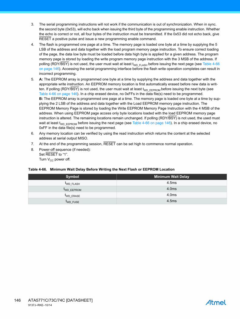
3. The serial programming instructions will not work if the communication is out of synchronization. When in sync. the second byte (0x53), will echo back when issuing the third byte of the programming enable instruction. Whether the echo is correct or not, all four bytes of the instruction must be transmitted. If the 0x53 did not echo back, give RESET a positive pulse and issue a new programming enable command.
4. The flash is programmed one page at a time. The memory page is loaded one byte at a time by supplying the 5 LSB of the address and data together with the load program memory page instruction. To ensure correct loading of the page, the data low byte must be loaded before data high byte is applied for a given address. The program memory page is stored by loading the write program memory page instruction with the 3 MSB of the address. If polling (RDY/BSY) is not used, the user must wait at least tWD_FLASH before issuing the next page (see Table 4-66 on page 146). Accessing the serial programming interface before the flash write operation completes can result in incorrect programming.
5. A: The EEPROM array is programmed one byte at a time by supplying the address and data together with the appropriate write instruction. An EEPROM memory location is first automatically erased before new data is writ-ten. If polling (RDY/BSY) is not used, the user must wait at least tWD_EEPROM before issuing the next byte (see Table 4-66 on page 146). In a chip erased device, no 0xFFs in the data file(s) need to be programmed.B: The EEPROM array is programmed one page at a time. The memory page is loaded one byte at a time by sup-plying the 2 LSB of the address and data together with the Load EEPROM memory page instruction. The EEPROM Memory Page is stored by loading the Write EEPROM Memory Page Instruction with the 4 MSB of the address. When using EEPROM page access only byte locations loaded with the load EEPROM memory page instruction is altered. The remaining locations remain unchanged. If polling (RDY/BSY) is not used, the used must wait at least tWD_EEPROM before issuing the next page (see Table 4-66 on page 146). In a chip erased device, no 0xFF in the data file(s) need to be programmed.
6. Any memory location can be verified by using the read instruction which returns the content at the selected address at serial output MISO.
7. At the end of the programming session, RESET can be set high to commence normal operation.
8. Power-off sequence (if needed):Set RESET to “1”.Turn VCC power off.
Table 4-66. Minimum Wait Delay Before Writing the Next Flash or EEPROM Location
Symbol Minimum Wait Delay
tWD_FLASH 4.5ms
tWD_EEPROM 4.0ms
tWD_ERASE 4.0ms
tWD_FUSE 4.5ms
ATA5771C/73C/74C [DATASHEET]9137J–RKE–10/14
146

4.23.6.2 Serial Programming Instruction set
Table 4-67 and Figure 4-74 on page 148 describes the Instruction set.
Notes: 1. Not all instructions are applicable for all parts.
2. a = address
3. Bits are programmed ‘0’, unprogrammed ‘1’.
4. To ensure future compatibility, unused fuses and lock bits should be unprogrammed (‘1’).
5. Refer to the corresponding section for fuse and lock bits, calibration and signature bytes and page size.
6. Instructions accessing program memory use a word address. This address may be random within the page range.
7. See http://www.atmel.com/avr for Application Notes regarding programming and programmers.
Table 4-67. Serial Programming Instruction Set
Instruction/Operation(1)
Instruction Format
Byte 1 Byte 2 Byte 3 Byte4
Programming enable $AC $53 $00 $00
Chip erase (program memory/EEPROM) $AC $80 $00 $00
Poll RDY/BSY $F0 $00 $00 data byte out
Load Instructions
Load extended address byte $4D $00 Extended adr $00
Load program memory page, high byte $48 adrmsB adr LSB high data byte in
Load program memory page, low byte $40 adrmsB adr LSB low data byte in
Load EEPROM Memory Page (page access) $C1 $00 adr LSB data byte in
Read Instructions
Read program memory, high byte $28 adrmsB adr LSB high data byte out
Read program memory, low byte $20 adrmsB adr LSB low data byte out
Read EEPROM memory $A0 $00 adr LSB data byte out
Read lock bits $58 $00 $00 data byte out
Read signature byte $30 $00 adr LSB data byte out
Read fuse bits $50 $00 $00 data byte out
Read fuse high bits $58 $08 $00 data byte out
Read extended fuse bits $50 $08 $00 data byte out
Read calibration byte $38 $00 $00 data byte out
Write Instructions(6)
Write program memory page $4C adrmsB adr LSB $00
Write EEPROM memory $C0 $00 adr LSB data byte in
Write EEPROM memory page (page access) $C2 $00 adr LSB $00
Write lock bits $AC $E0 $00 data byte in
Write fuse bits $AC $A0 $00 data byte in
Write fuse high bits $AC $A8 $00 data byte in
Write extended fuse bits $AC $A4 $00 data byte in
147ATA5771C/73C/74C [DATASHEET]9137J–RKE–10/14

If the LSB in RDY/BSY data byte out is ‘1’, a programming operation is still pending. Wait until this bit returns ‘0’ before the next instruction is carried out.
Within the same page, the low data byte must be loaded prior to the high data byte.
After data is loaded to the page buffer, program the EEPROM page, see Figure 4-74.
Figure 4-74. Serial Programming Instruction Example
4.23.7 High-voltage Serial Programming
This section describes how to program and verify flash program memory, EEPROM data memory, lock bits and fuse bits in the Atmel® ATtiny44V.
Figure 4-75. High-voltage Serial Programming
Byte 1 Byte 2 Byte 3 Byte 4
Page 0
Page 1
Page 2
Adr LBSAdr MBS
Bit 15 B 0 Bit 15 B 0
Byte 1 Byte 2 Byte 3 Byte 4
Adr LBSAdr MBS
Page N-1
Program Memory EEPROM Memory
Serial Programming Instruction
Page Buffer
Page Number
Page Offset
Load Program Memory Page (High/Low Byte)/Load EEPROM Memory Page (page access)
Write Program Memory Page/Write EEPROM Memory Page
GND
PB0
PB3 (RESET) VCC
SCI SDO
SII
SDI
+ 3.0 to 3.5V+ 11.5 to 12.5V
PA4
PA5
PA6
ATA5771C/73C/74C [DATASHEET]9137J–RKE–10/14
148

The minimum period for the serial clock input (SCI) during high-voltage serial programming is 220ns.
4.23.8 High-voltage Serial Programming Algorithm
To program and verify the Atmel® ATtiny44V in the high-voltage serial programming mode, the following sequence is recommended (see instruction formats in Table 4-71 on page 152).
4.23.8.1 Enter High-voltage Serial Programming Mode
The following algorithm puts the device in high-voltage serial programming mode:
1. Apply 4.5 to 5.5V between VCC and GND.
2. Set RESET pin to “0” and toggle SCI at least six times.
3. Set the Prog_enable pins listed in Table 4-69 on page 149 to “000” and wait at least 100ns.
4. Apply VHVRST – 5.5V to RESET. Keep the Prog_enable pins unchanged for at least tHVRST after the high-voltage has been applied to ensure the Prog_enable signature has been latched.
5. Shortly after latching the Prog_enable signature, the device will activly output data on the Prog_enable[2]/SDO pin, and the resulting drive contention may increase the power consumption. To minimize this drive contention, release the Prog_enable[2] pin after tHVRST has elapsed.
6. Wait at least 50µs before giving any serial instructions on SDI/SII.
4.23.8.2 Considerations for Efficient Programming
The loaded command and address are retained in the device during programming. For efficient programming, the following should be considered.
● The command needs only be loaded once when writing or reading multiple memory locations.
● Skip writing the data value 0xFF that is the contents of the entire EEPROM (unless the EESAVE fuse is programmed) and Flash after a chip erase.
● Address high byte needs only be loaded before programming or reading a new 256 word window in flash or 256 byte EEPROM. This consideration also applies to signature bytes reading.
Table 4-68. Pin Name Mapping
Signal Name in High-voltage Serial Programming Mode Pin Name I/O Function
SDI PA6 I Serial data input
SII PA5 I Serial instruction input
SDO PA4 O Serial data output
SCI PB0 I Serial clock input (min. 220ns period)
Table 4-69. Pin Values Used to Enter Programming Mode
Pin Symbol Value
PA0 Prog_enable[0] 0
PA1 Prog_enable[1] 0
PA2 Prog_enable[2] 0
Table 4-70. High-voltage Reset Characteristics
Supply Voltage RESET Pin High-voltage ThresholdMinimum High-voltage Period for Latching
Prog_enable
VCC VHVRST tHVRST
4.5V 11.5V 100ns
5.5V 11.5V 100ns
149ATA5771C/73C/74C [DATASHEET]9137J–RKE–10/14
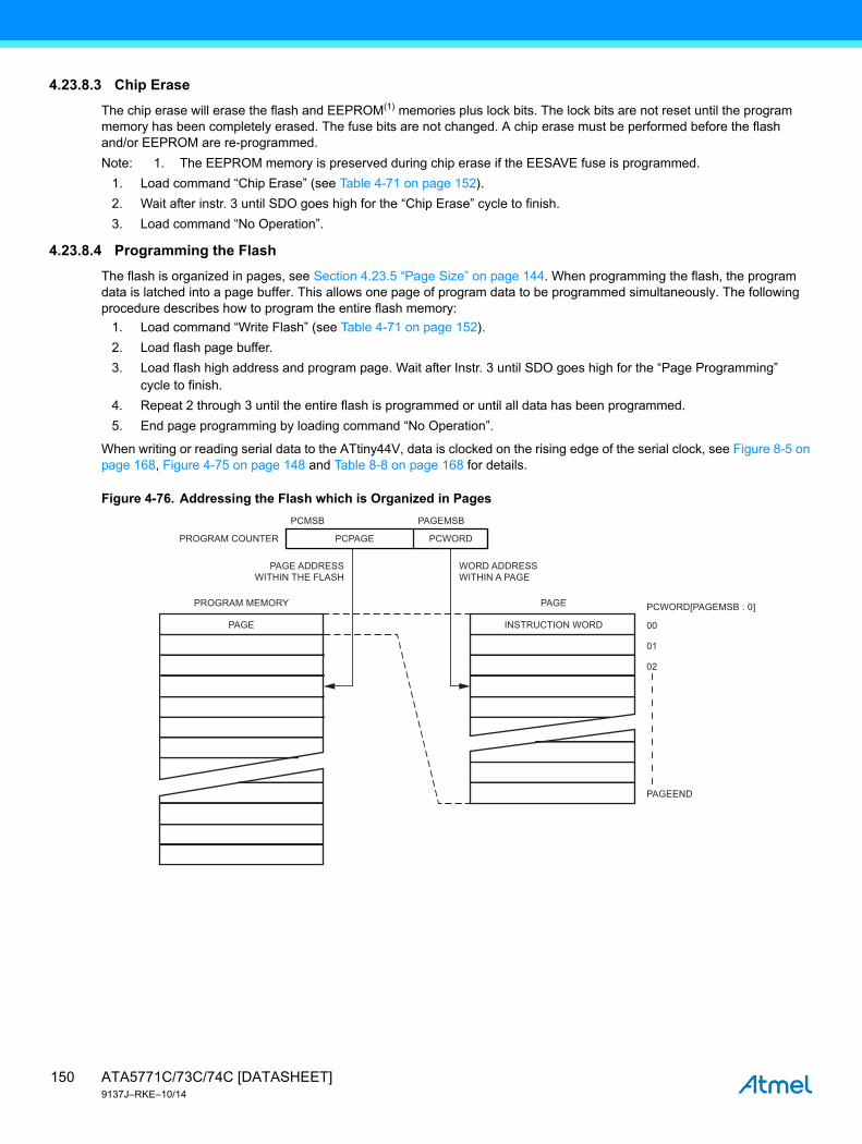
4.23.8.3 Chip Erase
The chip erase will erase the flash and EEPROM(1) memories plus lock bits. The lock bits are not reset until the program memory has been completely erased. The fuse bits are not changed. A chip erase must be performed before the flash and/or EEPROM are re-programmed.
Note: 1. The EEPROM memory is preserved during chip erase if the EESAVE fuse is programmed.
1. Load command “Chip Erase” (see Table 4-71 on page 152).
2. Wait after instr. 3 until SDO goes high for the “Chip Erase” cycle to finish.
3. Load command “No Operation”.
4.23.8.4 Programming the Flash
The flash is organized in pages, see Section 4.23.5 “Page Size” on page 144. When programming the flash, the program data is latched into a page buffer. This allows one page of program data to be programmed simultaneously. The following procedure describes how to program the entire flash memory:
1. Load command “Write Flash” (see Table 4-71 on page 152).
2. Load flash page buffer.
3. Load flash high address and program page. Wait after Instr. 3 until SDO goes high for the “Page Programming” cycle to finish.
4. Repeat 2 through 3 until the entire flash is programmed or until all data has been programmed.
5. End page programming by loading command “No Operation”.
When writing or reading serial data to the ATtiny44V, data is clocked on the rising edge of the serial clock, see Figure 8-5 on page 168, Figure 4-75 on page 148 and Table 8-8 on page 168 for details.
Figure 4-76. Addressing the Flash which is Organized in Pages
PAGEMSBPCMSB
WORD ADDRESSWITHIN A PAGE
PAGE ADDRESSWITHIN THE FLASH
PCWORDPCPAGE
PAGE INSTRUCTION WORD
PROGRAM MEMORY PAGE
PROGRAM COUNTER
02
01
00
PAGEEND
PCWORD[PAGEMSB : 0]
ATA5771C/73C/74C [DATASHEET]9137J–RKE–10/14
150
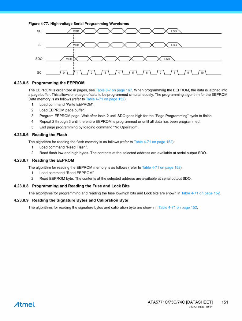
Figure 4-77. High-voltage Serial Programming Waveforms
4.23.8.5 Programming the EEPROM
The EEPROM is organized in pages, see Table 8-7 on page 167. When programming the EEPROM, the data is latched into a page buffer. This allows one page of data to be programmed simultaneously. The programming algorithm for the EEPROM Data memory is as follows (refer to Table 4-71 on page 152):
1. Load command “Write EEPROM”.
2. Load EEPROM page buffer.
3. Program EEPROM page. Wait after instr. 2 until SDO goes high for the “Page Programming” cycle to finish.
4. Repeat 2 through 3 until the entire EEPROM is programmed or until all data has been programmed.
5. End page programming by loading command “No Operation”.
4.23.8.6 Reading the Flash
The algorithm for reading the flash memory is as follows (refer to Table 4-71 on page 152):
1. Load command “Read Flash”.
2. Read flash low and high bytes. The contents at the selected address are available at serial output SDO.
4.23.8.7 Reading the EEPROM
The algorithm for reading the EEPROM memory is as follows (refer to Table 4-71 on page 152):
1. Load command “Read EEPROM”.
2. Read EEPROM byte. The contents at the selected address are available at serial output SDO.
4.23.8.8 Programming and Reading the Fuse and Lock Bits
The algorithms for programming and reading the fuse low/high bits and Lock bits are shown in Table 4-71 on page 152.
4.23.8.9 Reading the Signature Bytes and Calibration Byte
The algorithms for reading the signature bytes and calibration byte are shown in Table 4-71 on page 152.
0 1 2 3
MSB LSB
MSB LSB
MSB LSB
4 5 6 7 8 9 10
SDI
SII
SDO
SCI
151ATA5771C/73C/74C [DATASHEET]9137J–RKE–10/14

4.23.8.10 Power-off sequence
Set SCI to “0”. Set RESET to “1”. Turn VCC power off.
Table 4-71. High-voltage Serial Programming Instruction Set for Atmel ATtiny44V
Instruction
Instruction Format
Operation RemarksInstr.1/5 Instr.2/6 Instr.3/7 Instr.4
Chip erase
SDI
SII
SDO
0_1000_0000_00
0_0100_1100_00
x_xxxx_xxxx_xx
0_0000_0000_00
0_0110_0100_00
x_xxxx_xxxx_xx
0_0000_0000_00
0_0110_1100_00
x_xxxx_xxxx_xx
Wait after Instr.3 until SDO goes high for the chip erase cycle to finish.
Load “Write Flash” command
SDI
SII
SDO
0_0001_0000_00
0_0100_1100_00
x_xxxx_xxxx_xx
Enter flash programming code.
Load flash page buffer
SDI
SII
SDO
0_ bbbb_bbbb _00
0_0000_1100_00
x_xxxx_xxxx_xx
0_eeee_eeee_00
0_0010_1100_00
x_xxxx_xxxx_xx
0_0000_0000_00
0_0110_1101_00
x_xxxx_xxxx_xx
0_0000_0000_00
0_0110_1100_00
x_xxxx_xxxx_xx
Repeat after Instr. 1 - 7until the entire page buffer is filled or until all data within the page is filled. See Note 1.
SDI
SII
SDO
0_dddd_dddd_00
0_0011_1100_00
x_xxxx_xxxx_xx
0_0000_0000_00
0_0111_1101_00
x_xxxx_xxxx_xx
0_0000_0000_00
0_0111_1100_00
x_xxxx_xxxx_xx
Instr 5-7.
Load flash high address and program page
SDI
SII
SDO
0_0000_000a_00
0_0001_1100_00
x_xxxx_xxxx_xx
0_0000_0000_00
0_0110_0100_00
x_xxxx_xxxx_xx
0_0000_0000_00
0_0110_1100_00
x_xxxx_xxxx_xx
Wait after instr 3 until SDO goes high. Repeat instr. 2 - 3 for each loaded flash page until the entire flash or all data is programmed. Repeat instr. 1 for a new 256 byte page. See Note 1.
Load “Read Flash” command
SDI
SII
SDO
0_0000_0010_00
0_0100_1100_00
x_xxxx_xxxx_xx
Enter flash read mode.
Read flash low and high bytes
SDI
SII
SDO
0_bbbb_bbbb_00
0_0000_1100_00
x_xxxx_xxxx_xx
0_0000_000a_00
0_0001_1100_00
x_xxxx_xxxx_xx
0_0000_0000_00
0_0110_1000_00
x_xxxx_xxxx_xx
0_0000_0000_00
0_0110_1100_00
q_qqqq_qqqx_xx
Repeat instr. 1, 3 - 6 for each new address. Repeat instr. 2 for a new 256 byte page.
SDI
SII
SDO
0_0000_0000_00
0_0111_1000_00
x_xxxx_xxxx_xx
0_0000_0000_00
0_0111_1100_00
p_pppp_pppx_xx
Instr 5 - 6.
Load “Write EEPROM” command
SDI
SII
SDO
0_0001_0001_00
0_0100_1100_00
x_xxxx_xxxx_xx
Enter EEPROM programming mode.
a = address high bits, b = address low bits, d = data in high bits, e = data in low bits, p = data out high bits, q = data out low bits,x = don’t care, 1 = Lock Bit1, 2 = Lock Bit2, 3 = CKSEL0 Fuse, 4 = CKSEL1 Fuse, 5 = CKSEL2 Fuse, 6 = CKSEL3 Fuse, 7 = SUT0 Fuse, 8 = SUT1 Fuse, 9 = CKDIV8 Fuse, A = CKOUT Fuse, B = BODLEVEL0 Fuse, C = BODLEVEL1 Fuse, D= BODLEVEL2 Fuse, E = EESAVE Fuse, F = WDTON Fuse, G = SPIEN Fuse, H = DWEN Fuse, I = RSTDISBL Fuse
Notes: 1. For page sizes less than 256 words, parts of the address (bbbb_bbbb) will be parts of the page address.
2. For page sizes less than 256 bytes, parts of the address (bbbb_bbbb) will be parts of the page address.
3. The EEPROM is written page-wise. But only the bytes that are loaded into the page are actually written to the EEPROM. Page-wise EEPROM access is more efficient when multiple bytes are to be written to the same page. Note that auto-erase of EEPROM is not available in high-voltage serial programming, only in SPI programming.
ATA5771C/73C/74C [DATASHEET]9137J–RKE–10/14
152
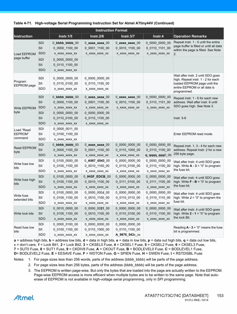
Load EEPROM page buffer
SDI
SII
SDO
0_bbbb_bbbb_00
0_0000_1100_00
x_xxxx_xxxx_xx
0_aaaa_aaaa_00
0_0001_1100_00
x_xxxx_xxxx_xx
0_eeee_eeee_00
0_0010_1100_00
x_xxxx_xxxx_xx
0_0000_0000_00
0_0110_1101_00
x_xxxx_xxxx_xx
Repeat instr. 1 - 5 until the entire page buffer is filled or until all data within the page is filled. See Note 2.
SDI
SII
SDO
0_0000_0000_00
0_0110_1100_00
x_xxxx_xxxx_xx
Program EEPROM page
SDI
SII
SDO
0_0000_0000_00
0_0110_0100_00
x_xxxx_xxxx_xx
0_0000_0000_00
0_0110_1100_00
x_xxxx_xxxx_xx
Wait after instr. 2 until SDO goes high. Repeat instr. 1 - 2 for each loaded EEPROM page until the entire EEPROM or all data is programmed.
Write EEPROM byte
SDI
SII
SDO
0_bbbb_bbbb_00
0_0000_1100_00
x_xxxx_xxxx_xx
0_aaaa_aaaa_00
0_0001_1100_00
x_xxxx_xxxx_xx
0_eeee_eeee_00
0_0010_1100_00
x_xxxx_xxxx_xx
0_0000_0000_00
0_0110_1101_00
x_xxxx_xxxx_xx
Repeat instr. 1 - 6 for each new address. Wait after instr. 6 until SDO goes high. See Note 3.
SDI
SII
SDO
0_0000_0000_00
0_0110_0100_00
x_xxxx_xxxx_xx
0_0000_0000_00
0_0110_1100_00
x_xxxx_xxxx_xx
Instr. 5-6
Load “Read EEPROM” command
SDI
SII
SDO
0_0000_0011_00
0_0100_1100_00
x_xxxx_xxxx_xx
Enter EEPROM read mode.
Read EEPROM byte
SDI
SII
SDO
0_bbbb_bbbb_00
0_0000_1100_00
x_xxxx_xxxx_xx
0_aaaa_aaaa_00
0_0001_1100_00
x_xxxx_xxxx_xx
0_0000_0000_00
0_0110_1000_00
x_xxxx_xxxx_xx
0_0000_0000_00
0_0110_1100_00
q_qqqq_qqq0_00
Repeat instr. 1, 3 - 4 for each new address. Repeat Instr. 2 for a new 256 byte page.
Write fuse low bits
SDI
SII
SDO
0_0100_0000_00
0_0100_1100_00
x_xxxx_xxxx_xx
0_A987_6543_00
0_0010_1100_00
x_xxxx_xxxx_xx
0_0000_0000_00
0_0110_0100_00
x_xxxx_xxxx_xx
0_0000_0000_00
0_0110_1100_00
x_xxxx_xxxx_xx
Wait after Instr. 4 until SDO goes high. Write A - 3 = “0” to program the fuse bit.
Write fuse high bits
SDI
SII
SDO
0_0100_0000_00
0_0100_1100_00
x_xxxx_xxxx_xx
0_IHGF_EDCB_00
0_0010_1100_00
x_xxxx_xxxx_xx
0_0000_0000_00
0_0111_0100_00
x_xxxx_xxxx_xx
0_0000_0000_00
0_0111_1100_00
x_xxxx_xxxx_xx
Wait after instr. 4 until SDO goes high. Write F - B = “0” to program the fuse bit.
Write fuse extended bits
SDI
SII
SDO
0_0100_0000_00
0_0100_1100_00
x_xxxx_xxxx_xx
0_0000_000J_00
0_0010_1100_00
x_xxxx_xxxx_xx
0_0000_0000_00
0_0110_0110_00
x_xxxx_xxxx_xx
0_0000_0000_00
0_0110_1110_00
x_xxxx_xxxx_xx
Wait after Instr. 4 until SDO goes high. Write J = “0” to program the fuse bit.
Write lock bits
SDI
SII
SDO
0_0010_0000_00
0_0100_1100_00
x_xxxx_xxxx_xx
0_0000_0021_00
0_0010_1100_00
x_xxxx_xxxx_xx
0_0000_0000_00
0_0110_0100_00
x_xxxx_xxxx_xx
0_0000_0000_00
0_0110_1100_00
x_xxxx_xxxx_xx
Wait after Instr. 4 until SDO goes high. Write 2 - 1 = “0” to program the lock Bit.
Read fuse low bits
SDI
SII
SDO
0_0000_0100_00
0_0100_1100_00
x_xxxx_xxxx_xx
0_0000_0000_00
0_0110_1000_00
x_xxxx_xxxx_xx
0_0000_0000_00
0_0110_1100_00
A_9876_543x_xx
Reading A - 3 = “0” means the fuse bit is programmed.
Table 4-71. High-voltage Serial Programming Instruction Set for Atmel ATtiny44V (Continued)
Instruction
Instruction Format
Operation RemarksInstr.1/5 Instr.2/6 Instr.3/7 Instr.4
a = address high bits, b = address low bits, d = data in high bits, e = data in low bits, p = data out high bits, q = data out low bits,x = don’t care, 1 = Lock Bit1, 2 = Lock Bit2, 3 = CKSEL0 Fuse, 4 = CKSEL1 Fuse, 5 = CKSEL2 Fuse, 6 = CKSEL3 Fuse, 7 = SUT0 Fuse, 8 = SUT1 Fuse, 9 = CKDIV8 Fuse, A = CKOUT Fuse, B = BODLEVEL0 Fuse, C = BODLEVEL1 Fuse, D= BODLEVEL2 Fuse, E = EESAVE Fuse, F = WDTON Fuse, G = SPIEN Fuse, H = DWEN Fuse, I = RSTDISBL Fuse
Notes: 1. For page sizes less than 256 words, parts of the address (bbbb_bbbb) will be parts of the page address.
2. For page sizes less than 256 bytes, parts of the address (bbbb_bbbb) will be parts of the page address.
3. The EEPROM is written page-wise. But only the bytes that are loaded into the page are actually written to the EEPROM. Page-wise EEPROM access is more efficient when multiple bytes are to be written to the same page. Note that auto-erase of EEPROM is not available in high-voltage serial programming, only in SPI programming.
153ATA5771C/73C/74C [DATASHEET]9137J–RKE–10/14

Read fuse high bits
SDI
SII
SDO
0_0000_0100_00
0_0100_1100_00
x_xxxx_xxxx_xx
0_0000_0000_00
0_0111_1010_00
x_xxxx_xxxx_xx
0_0000_0000_00
0_0111_1100_00
I_HGFE_DCBx_xx
Reading F - B = “0” means the fuse bit is programmed.
Read fuse extended bits
SDI
SII
SDO
0_0000_0100_00
0_0100_1100_00
x_xxxx_xxxx_xx
0_0000_0000_00
0_0110_1010_00
x_xxxx_xxxx_xx
0_0000_0000_00
0_0110_1110_00
x_xxxx_xxJx_xx
Reading J = “0” means the fuse bit is programmed.
Read lock bits
SDI
SII
SDO
0_0000_0100_00
0_0100_1100_00
x_xxxx_xxxx_xx
0_0000_0000_00
0_0111_1000_00
x_xxxx_xxxx_xx
0_0000_0000_00
0_0110_1100_00
x_xxxx_x21x_xx
Reading 2, 1 = “0” means the Lock bit is programmed.
Read signature bytes
SDI
SII
SDO
0_0000_1000_00
0_0100_1100_00
x_xxxx_xxxx_xx
0_0000_00bb_00
0_0000_1100_00
x_xxxx_xxxx_xx
0_0000_0000_00
0_0110_1000_00
x_xxxx_xxxx_xx
0_0000_0000_00
0_0110_1100_00
q_qqqq_qqqx_xx
Repeats instr 2 4 for each signature byte address.
Read calibration byte
SDI
SII
SDO
0_0000_1000_00
0_0100_1100_00
x_xxxx_xxxx_xx
0_0000_0000_00
0_0000_1100_00
x_xxxx_xxxx_xx
0_0000_0000_00
0_0111_1000_00
x_xxxx_xxxx_xx
0_0000_0000_00
0_0111_1100_00
p_pppp_pppx_xx
Load “No Operation” command
SDI
SII
SDO
0_0000_0000_00
0_0100_1100_00
x_xxxx_xxxx_xx
Table 4-71. High-voltage Serial Programming Instruction Set for Atmel ATtiny44V (Continued)
Instruction
Instruction Format
Operation RemarksInstr.1/5 Instr.2/6 Instr.3/7 Instr.4
a = address high bits, b = address low bits, d = data in high bits, e = data in low bits, p = data out high bits, q = data out low bits,x = don’t care, 1 = Lock Bit1, 2 = Lock Bit2, 3 = CKSEL0 Fuse, 4 = CKSEL1 Fuse, 5 = CKSEL2 Fuse, 6 = CKSEL3 Fuse, 7 = SUT0 Fuse, 8 = SUT1 Fuse, 9 = CKDIV8 Fuse, A = CKOUT Fuse, B = BODLEVEL0 Fuse, C = BODLEVEL1 Fuse, D= BODLEVEL2 Fuse, E = EESAVE Fuse, F = WDTON Fuse, G = SPIEN Fuse, H = DWEN Fuse, I = RSTDISBL Fuse
Notes: 1. For page sizes less than 256 words, parts of the address (bbbb_bbbb) will be parts of the page address.
2. For page sizes less than 256 bytes, parts of the address (bbbb_bbbb) will be parts of the page address.
3. The EEPROM is written page-wise. But only the bytes that are loaded into the page are actually written to the EEPROM. Page-wise EEPROM access is more efficient when multiple bytes are to be written to the same page. Note that auto-erase of EEPROM is not available in high-voltage serial programming, only in SPI programming.
ATA5771C/73C/74C [DATASHEET]9137J–RKE–10/14
154

5. Application
Figure 5-1 illustrates a principle application circuit using loop antenna. For the blocking measure of the power supply voltage, a capacitor value of C3 = 68nF/X7R is recommended. C1 and C2 are used to match the loop antenna to the power amplifier. Two capacitors in series should be used to achieve a better tolerance value for C2 and allowing the possibility of realizing the ZLoad,opt using standard valued capacitors.
Figure 5-1. The Principle Application Circuit Using a Loop Antenna for ASK Modulation
Together with the pins and the PCB board wires C1 forms a series resonance loop that suppress the 1st harmonic. Therefore the position of C1 on the PCB is important. Generally the best suppression is achieved when C1 is placed as close as possible to the pins ANT1 and ANT2.
The loop antenna should not exceed a width of 1.5 mm, otherwise the Q-factor of the loop antenna is too high.
The capacitor C4 should be selected that the XTO runs on the load resonance frequency of the crystal.
Atmel ATA57771/73/74
LoopAntenna
VS
VSVCC_RF
GND_RF
PA_ENABLE
ENABLE
XTO
PA
VCO
f/4 PLL
Powerup/Down
ANT1
ANT2
PXYS1
S1
S1
PXY
PXY
PXY
PXY
PXY
PXY
VDD
GND
PXY
PXY
PXY
PXY
PXY
VS
CLK
C4
C2
C1
155ATA5771C/73C/74C [DATASHEET]9137J–RKE–10/14

Figure 5-2. Typical ASK Application Atmel ATA577x
Table 5-1. Bill of Material
Component ValueType/
Manufacturer Note
315MHz 433.92MHz 868.3MHz
L1 100nH 82nH 22nHLL1608-FSL/
TOKO
L2 39nH 27nH 2.2nHLL1608-FSL/
TOKO
C1 1nF 1nF 1nFGRM1885C/
Murata
C2 3.9pF 2.7pF 1.5pFGRM1885C/
MurataThis cap must be placed as close as possible to the pin Ant1 and Ant2
C3 27pF 16pF 4.3pFGRM1885C/
Murata
On the demo board 2 capacitors in series are used to reduce the tolerance
C4 3.9pF 1.6pF 0.3pF GRM1885C/
Murata
On the demo board 2 capacitors in series are used to reduce the tolerance
C5 68nF 68nF 68nFGRM188R71C/
MurataThis cap must placed as close as possible to the VCC_RF
C6 100nF 100nF 100nFGRM188R71C /
MurataThis cap must placed as close as possible to the VDD
PB0/XTAL1
VDD
PB3/RESET
PB2
PA7ADC7
GN
D_R
F
GN
D
XTA
L
VC
C_R
F
EN
AB
LE
GN
D
PA_E
NA
BLE
GN
D
AN
T1
AN
T2
CLK
PA6
AD
C6
PB1/XTAL2
PA1/ADC1
PA0/ADC0
23
PA3/ADC3
PA4/ADC4
PA5/ADC5
PA2/ADC2
C5
VCC
VCC
VCC
L1
ATA577x
SW1
SW3
SW2
C8
Q1
C6R3
C7
R2
C4C3C2L2
C1
R1
ATA5771C/73C/74C [DATASHEET]9137J–RKE–10/14
156

Figure 5-3. Typical FSK Application Atmel ATA577x
Note: FSK Modulation is achieved by switching on and off an additional capacitor between the XTAL load capacitor and GND. This is done using a MOS switch controlled by a microcontroller output.
C7 100nF 100nF 100nFGRM188R71C/
Murata
C8 10pF 12pF 12pFGRM1885C/
Murata
Q1 9.843750MHz 13.56MHz 13.567187MHzDSX530GK/
KDS
R1 100kΩ 100kΩ 100kΩ
R2 100kΩ 100kΩ 100kΩ
R3 10kΩ 10kΩ 10kΩ
Table 5-1. Bill of Material (Continued)
Component ValueType/
Manufacturer Note
PB0/XTAL1
VDD
PB3/RESET
PB2
PA7ADC7
GN
D_R
F
GN
D
XTA
L
VC
C_R
F
EN
AB
LE
GN
D
PA_E
NA
BLE
GN
D
AN
T1
AN
T2
CLK
PA6
AD
C6
PB1/XTAL2
PA1/ADC1
PA0/ADC0
PA3/ADC3
PA4/ADC4
PA5/ADC5
PA2/ADC2
C5
VCC
VCC
VCC
ATA577x
SW1
SW3
SW2
T1
C9Q1
C8
C6C7
R3
R2 R1
C4C3C2
L1
L2
C1
157ATA5771C/73C/74C [DATASHEET]9137J–RKE–10/14
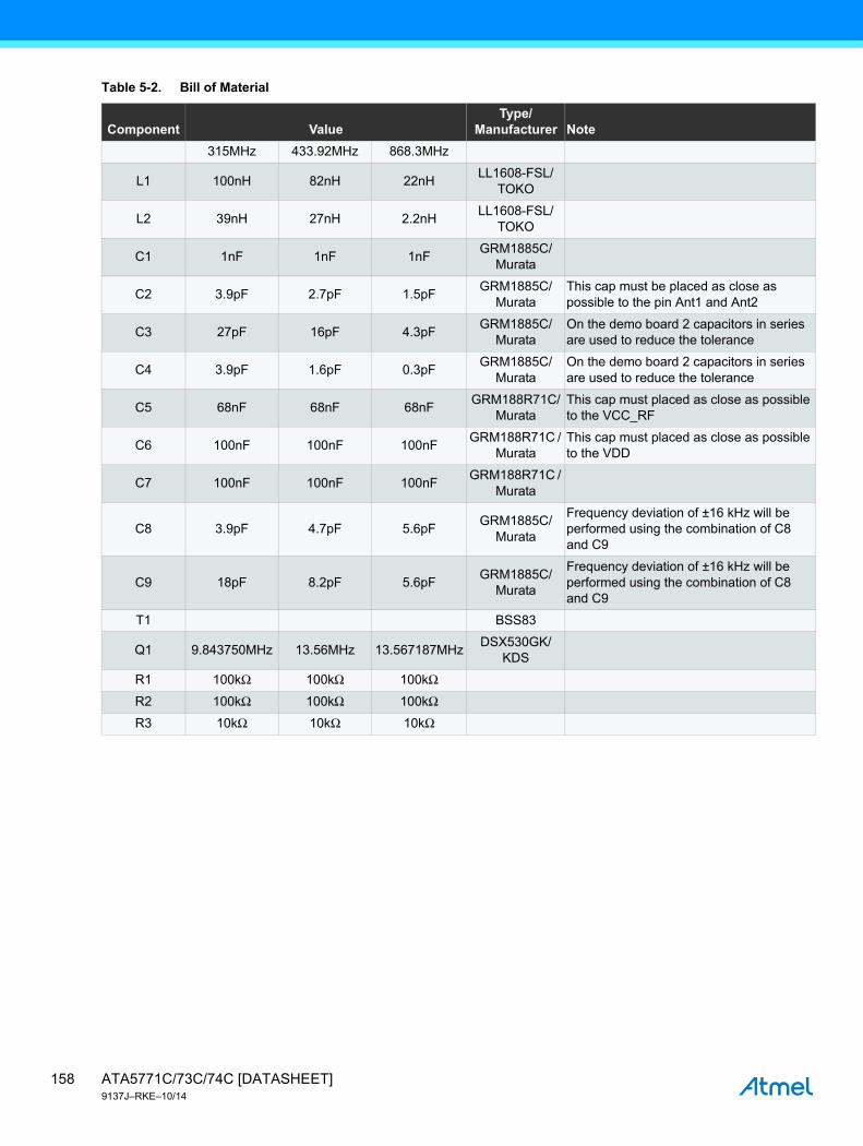
Table 5-2. Bill of Material
Component ValueType/
Manufacturer Note
315MHz 433.92MHz 868.3MHz
L1 100nH 82nH 22nHLL1608-FSL/
TOKO
L2 39nH 27nH 2.2nHLL1608-FSL/
TOKO
C1 1nF 1nF 1nFGRM1885C/
Murata
C2 3.9pF 2.7pF 1.5pFGRM1885C/
MurataThis cap must be placed as close as possible to the pin Ant1 and Ant2
C3 27pF 16pF 4.3pFGRM1885C/
MurataOn the demo board 2 capacitors in series are used to reduce the tolerance
C4 3.9pF 1.6pF 0.3pF GRM1885C/
MurataOn the demo board 2 capacitors in series are used to reduce the tolerance
C5 68nF 68nF 68nFGRM188R71C/
MurataThis cap must placed as close as possible to the VCC_RF
C6 100nF 100nF 100nFGRM188R71C /
MurataThis cap must placed as close as possible to the VDD
C7 100nF 100nF 100nFGRM188R71C /
Murata
C8 3.9pF 4.7pF 5.6pFGRM1885C/
Murata
Frequency deviation of ±16 kHz will be performed using the combination of C8 and C9
C9 18pF 8.2pF 5.6pFGRM1885C/
Murata
Frequency deviation of ±16 kHz will be performed using the combination of C8 and C9
T1 BSS83
Q1 9.843750MHz 13.56MHz 13.567187MHzDSX530GK/
KDS
R1 100kΩ 100kΩ 100kΩ
R2 100kΩ 100kΩ 100kΩ
R3 10kΩ 10kΩ 10kΩ
ATA5771C/73C/74C [DATASHEET]9137J–RKE–10/14
158

6. Absolute Maximum Ratings
Figure 6-1. ESD Protection Circuit of the Transmitter
6.1 RF Transmitter BlockStresses beyond those listed under “Absolute Maximum Ratings” may cause permanent damage to the device. This is a stress rating only and functional operation of the device at these or any other conditions beyond those indicated in the operational sections of this specification is not implied. Exposure to absolute maximum rating conditions for extended periods may affect device reliability.
Parameters Symbol Minimum Maximum Unit
Supply voltage VS 5 V
Power dissipation Ptot 100 mW
Junction temperature Tj 150 °C
Storage temperature Tstg –55 +125 °C
Ambient temperature Tamb –55 +125 °C
Input voltage VmaxPA_ENABLE –0.3 (VS + 0.3)(1) V
Note: 1. If VS + 0.3 is higher than 3.7V, the maximum voltage will be reduced to 3.7V
CLK
VS
GND
PA_ENABLE XTALANT2 ENABLE
ANT1
6.2 Microcontroller Block (Atmel ATtiny44V)Stresses beyond those listed under “Absolute Maximum Ratings” may cause permanent damage to the device. This is a stress rating only and functional operation of the device at these or any other conditions beyond those indicated in the operational sections of this specification is not implied. Exposure to absolute maximum rating conditions for extended periods may affect device reliability.
Parameters Min. Typ. Max. Unit
Operating temperature –40 +85 °C
Storage temperature –65 +175 °C
Voltage on any pin except RESET with respect to ground
–0.5 VCC + 0.5 V
Maximum operating voltage 6.0 V
Voltage on RESET with respect to ground –0.5 +13.0 V
Voltage on VCC with respect to ground –0.5 +6.0 V
DC current per I/O pin 30.0 mA
DC current VCC and GND pins 200.0 mA
Injection current at VCC = 0V to 5V(2) ±5.0 mA(1)
Notes: 1. Maximum current per port = ±30mA
2. Functional corruption may occur.
159ATA5771C/73C/74C [DATASHEET]9137J–RKE–10/14

8. Electrical Characteristics
7. Thermal Resistance
Parameters Symbol Value Unit
Junction ambient RthJA 35 K/W
8.1 The General Current Consumption Characteristic for Key Fob ApplicationVS = 2.0V to 3.6V, Tamb = –40°C to +85°C unless otherwise specified. Typical values are given at VS = 3.0V and Tamb = 25°C.
Transmitter (T5750/3/4)ATtiny44V
WDT Disabled Total
Power downTyp. < 10nA Typ. 0.2µA Typ. < 0.21µA
Max. 350nA Max. 3µA Max. 3.35µA
Active (VS = 3V; RC = 4MHz)
315MHz / 434MHz
Typ. 9mA Typ. 0.8mA Typ. 9.8mA
Max. 11.6mA Max. 2.5mA Max. 14.1mA
868MHzTyp. 8.5mA Typ. 0.8mA Typ. 9.3mA
Max. 11mA Max. 2.5mA Max. 13.5mA
Note: These values are based on the DC electrical values in Section 8.2 “RF Transmitter Block” on page 160 and Section 8.3 “Microcontroller Block” on page 162.
8.2 RF Transmitter Block VS = 2.0V to 3.6V, Tamb = –40°C to +85°C unless otherwise specified. Typical values are given at VS = 3.0V and Tamb = 25°C. All parameters are referred to GND (pin 7)
Parameters Test Conditions Symbol Min. Typ. Max. Unit
Supply current of RF transmitter block (* please take account an additional current consumption of the microcontroller block)
Power down, VENABLE < 0.25 V, –40°C to +85°CVPA-ENABLE < 0.25V, 25°C
IS_Off< 10
350 nAnA
Power up, PA off, VS = 3V,VENABLE > 1.7V, VPA-ENABLE < 0.25V315MHz/434MHz868MHz
IS3.73.6
4.8 4.6
mA
Power up, VS = 3.0V,VENABLE > 1.7V, VPA-ENABLE> 1.7V315MHz/434MHz868MHz
IS_Transmit 98.5
11.611
mA
Output power
VS = 3.0V, Tamb = 25°C,f = 315MHz, ZLoad = (255 + j192)Ωf = 433.92MHz, ZLoad = (166 + j233)Ωf = 868.3MHz, ZLoad = (166 + j226)Ω
PRef6.05.53.5
8.07.55.5
10.5108
dBm
Output power variation for the full temperature range
Tamb = –40°C to +85°C,VS = 3.0VVS = 2.0VPOut = PRef + ΔPRef
ΔPRefΔPRef
–1.5–4.0
dBdB
Achievable output-power range
Selectable by load impedance315MHz 434MHz868MHz
POut_typ00
–3
8.07.5
+5.5
dBm
Note: 1. If VS is higher than 3.6V, the maximum voltage will be reduced to 3.6V.
ATA5771C/73C/74C [DATASHEET]9137J–RKE–10/14
160
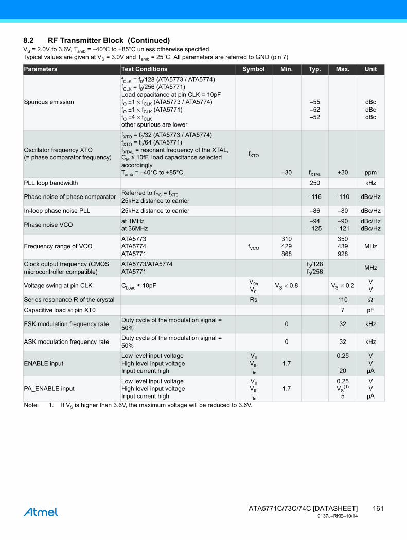
Spurious emission
fCLK = f0/128 (ATA5773 / ATA5774)fCLK = f0/256 (ATA5771)Load capacitance at pin CLK = 10pFfO ±1 × fCLK (ATA5773 / ATA5774)fO ±1 × fCLK (ATA5771)fO ±4 × fCLK other spurious are lower
–55–52–52
dBcdBcdBc
Oscillator frequency XTO (= phase comparator frequency)
fXTO = f0/32 (ATA5773 / ATA5774)fXTO = f0/64 (ATA5771)fXTAL = resonant frequency of the XTAL, CM ≤ 10fF, load capacitance selected accordingly Tamb = –40°C to +85°C
fXTO
–30 fXTAL +30 ppm
PLL loop bandwidth 250 kHz
Phase noise of phase comparatorReferred to fPC = fXT0,25kHz distance to carrier
–116 –110 dBc/Hz
In-loop phase noise PLL 25kHz distance to carrier –86 –80 dBc/Hz
Phase noise VCOat 1MHzat 36MHz
–94–125
–90–121
dBc/HzdBc/Hz
Frequency range of VCOATA5773ATA5774ATA5771
fVCO
310429868
350439928
MHz
Clock output frequency (CMOS microcontroller compatible)
ATA5773/ATA5774ATA5771
f0/128f0/256
MHz
Voltage swing at pin CLK CLoad ≤ 10pFV0hV0l
VS × 0.8 VS × 0.2VV
Series resonance R of the crystal Rs 110 Ω
Capacitive load at pin XT0 7 pF
FSK modulation frequency rateDuty cycle of the modulation signal = 50%
0 32 kHz
ASK modulation frequency rateDuty cycle of the modulation signal = 50%
0 32 kHz
ENABLE input Low level input voltageHigh level input voltageInput current high
VIlVIhIIn
1.70.25
20
VV
µA
PA_ENABLE inputLow level input voltageHigh level input voltageInput current high
VIlVIhIIn
1.70.25VS
(1)
5
VV
µA
8.2 RF Transmitter Block (Continued)VS = 2.0V to 3.6V, Tamb = –40°C to +85°C unless otherwise specified. Typical values are given at VS = 3.0V and Tamb = 25°C. All parameters are referred to GND (pin 7)
Parameters Test Conditions Symbol Min. Typ. Max. Unit
Note: 1. If VS is higher than 3.6V, the maximum voltage will be reduced to 3.6V.
161ATA5771C/73C/74C [DATASHEET]9137J–RKE–10/14
8.3 Microcontroller Block
8.3.1 DC Characteristics
TA = –40°C to +85°C, VCC = 2.0V to 3.6V (unless otherwise noted)(1)
Parameter Condition Symbol Min. Typ. Max. Unit
Input low voltage except XTAL1 and RESET pin
VCC = 1.8V to 3.6V TA = –40°C to +85°C
VIL –0.5 +0.2VCC(1) V
Input low voltage, XTAL1 pinVCC = 1.8V to 3.6VTA = –40°C to +85°C
VIL1 –0.5 +0.2VCC(1) V
Input high voltage, except XTAL1 and RESET pins
VCC = 1.8V to 3.6V TA = –40°C to +85°C
VIH 0.7VCC(1) VCC + 0.5 V
Input high voltage, XTAL1 pin
VCC = 1.8V to 3.6VTA = –40°C to +85°C
VIH1 0.9VCC(1) VCC + 0.5 V
Input low voltage, RESET pin
VCC = 1.8V to 3.6VTA = –40°C to +85°C
VIL2 –0.5 +0.2VCC(1) V
Input high voltage, RESET pin
VCC = 1.8V to 3.6VTA = –40°C to +85°C
VIH2 0.9VCC(1) VCC + 0.5 V
Output low voltage(2), I/O pin except RESET
IOL = 2mA, VCC = 1.8V VOL 0.2 V
Output high voltage(3), I/O pin except RESET
IOH = –2mA, VCC = 1.8V VOH 1.2 V
Reset pull-up resistor RRST 30 60 kΩ
I/O pin Pull-up resistor Rpu 20 50 kΩ
Power supply current
Active 4MHz, VCC = 3VTA = –40°C to +85°C
ICC
0.8 2.5 mA
Idle 4MHz, VCC = 3VTA = –40°C to +85°C
0.2 0.5 mA
Power-down modeWDT enabled, VCC = 3V 4 18 µA
WDT disabled, VCC = 3V 0.2 3 µA
Analog comparator Input offset voltage
VCC = 2.7VVin = VCC/2TA = –40°C to +85°C
VACIO < 10 40 mV
Analog comparator Input leakage current
VCC = 2.7VVin = VCC/2TA = –40°C to +85°CVCC = 1.8V to 3.6V
IACLK –50 +50 nA
Notes: 1. “Max” means the highest value where the pin is guaranteed to be read as low.
2. “Min” means the lowest value where the pin is guaranteed to be read as high.
3. Although each I/O port can sink more than the test conditions (10mA at VCC = 5V, 5mA at VCC = 3V) under steady state conditions (non-transient), the following must be observed:1] The sum of all IOL, for all ports, should not exceed 60mA.If IOL exceeds the test condition, VOL may exceed the related specification. Pins are not guaranteed to sink current greater than the listed test condition.
4. Although each I/O port can source more than the test conditions (10mA at VCC = 5V, 5mA at VCC = 3V) under steady state conditions (non-transient), the following must be observed:1] The sum of all IOH, for all ports, should not exceed 60mA.If IOH exceeds the test condition, VOH may exceed the related specification. Pins are not guaranteed to source current greater than the listed test condition. Pull up driving strength of the PB3 RESET pad is weak.
ATA5771C/73C/74C [DATASHEET]9137J–RKE–10/14
162
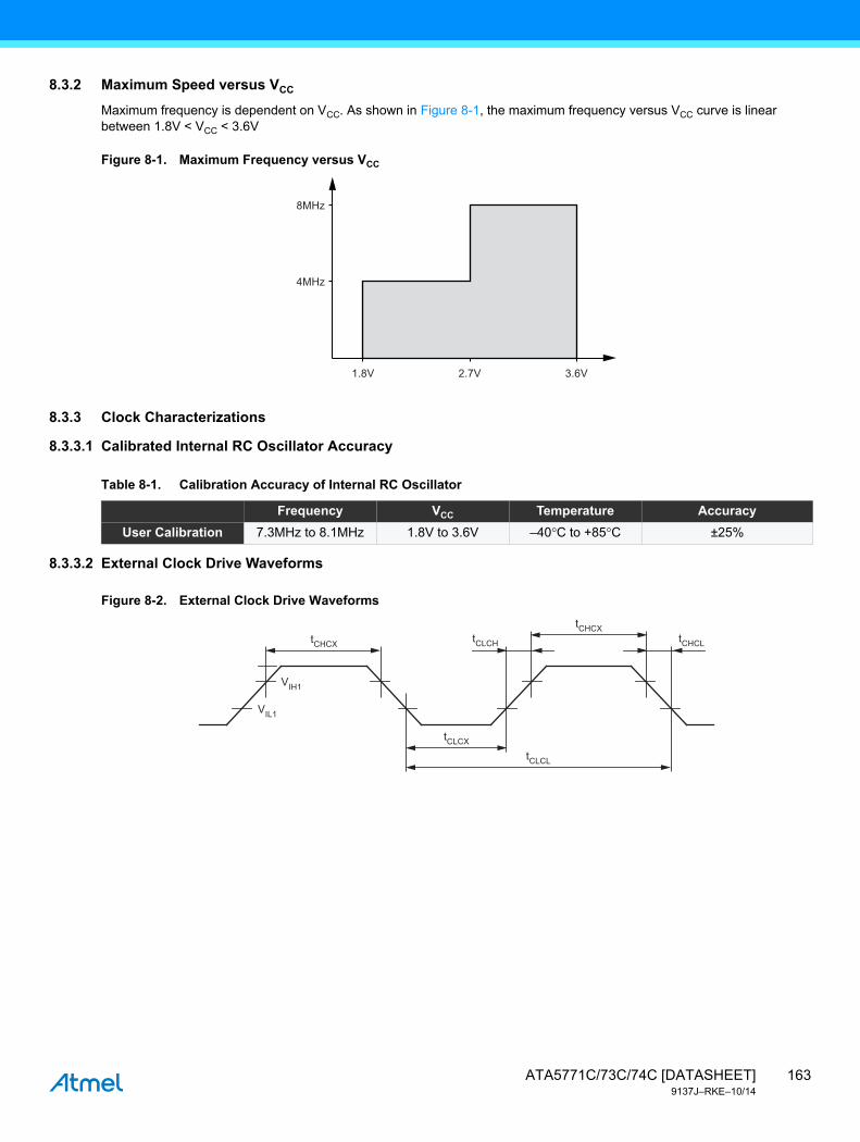
8.3.2 Maximum Speed versus VCC
Maximum frequency is dependent on VCC. As shown in Figure 8-1, the maximum frequency versus VCC curve is linear between 1.8V < VCC < 3.6V
Figure 8-1. Maximum Frequency versus VCC
8.3.3 Clock Characterizations
8.3.3.1 Calibrated Internal RC Oscillator Accuracy
8.3.3.2 External Clock Drive Waveforms
Figure 8-2. External Clock Drive Waveforms
8MHz
1.8V 2.7V 3.6V
4MHz
Table 8-1. Calibration Accuracy of Internal RC Oscillator
Frequency VCC Temperature Accuracy
User Calibration 7.3MHz to 8.1MHz 1.8V to 3.6V –40°C to +85°C ±25%
tCHCX
VIH1
VIL1
tCHCXtCLCH tCHCL
tCLCX
tCLCL
163ATA5771C/73C/74C [DATASHEET]9137J–RKE–10/14

8.3.3.3 External Clock Drive
8.3.4 System and Reset Characterizations
Table 8-2. External Clock Drive
Parameter Symbol
VCC = 2.7 - 3.6V
UnitMin. Max.
Clock frequency 1/tCLCL 0 10 MHz
Clock period tCLCL 100 ns
High time tCHCX 40 ns
Low time tCLCX 40 ns
Rise time tCLCH 1.6 µs
Fall time tCHCL 1.6 µs
Change in period from one clock cycle to the next ΔtCLCL 2 %
Table 8-3. Reset, Brown-out and Internal Voltage Reference Characteristics(1)
Parameter Condition Symbol Min Typ Max Unit
Brown-out detector hysteresis VHYST 100 250 mV
RAM retention voltage(1) VRAM(2) 50 mV
Min pulse width on brown-out reset tBOD 2 ns
Bandgap reference voltage VC C = 2.7V, TA = 25°C VBG 1.0 1.1 1.2 V
Bandgap reference start-up time VC C = 2.7V, TA = 25°C tBG 40 70 µs
Bandgap reference current consumption VC C = 2.7V, TA = 25°C IBG 10 µA
Notes: 1. Values are guidelines only.
2. This is the limit to which VDD can be lowered without losing RAM data
Table 8-4. BODLEVEL Fuse Coding(1)
BODLEVEL Min VBOT Typ VBOT Max VBOT Unit Type*
111 BOD disabled
110 1.7 1.8 2.0
V
A
001 1.7 1.9 2.1 C
000 1.8 2.0 2.2 C
010 2.0 2.2 2.4 C
011 2.1 2.3 2.5 C
101 2.5 2.7 2.9 A
*) Type means: A = 100% tested, C = Characterized on samples
Note: 1. VBOT may be below nominal minimum operating voltage for some devices. For devices where this is the case, the device is tested down to VCC = VBOT during the production test. This guarantees that a brown-out reset will occur before VCC drops to a voltage where correct operation of the microcontroller is no longer guaranteed
ATA5771C/73C/74C [DATASHEET]9137J–RKE–10/14
164

8.3.5 ADC Characteristics – Preliminary Data
Table 8-5. ADC Characteristics, Single Ended Channels. –40°C to +85°C, unless otherwise noted
Parameter Condition Symbol Min Typ Max Unit
Resolution Single ended conversion 10 Bits
Absolute accuracy (Including INL, DNL, quantization error, gain and offset error)
VCC = 1.8V, VRef = 1.8V, ADC clock = 200kHzTA = –40°C to +85°C
TUE
2 4.0 LSB
VCC = 1.8V, VRef = 1.8V, ADC clock = 200kHzNoise reduction modeTA = –40°C to +85°C
2 4.0 LSB
Integral non-linearity (INL)VCC = 1.8V, VRef = 1.8V, ADC clock = 200kHzTA = –40°C to +85°C
INL 0.5 1.5 LSB
Differential non-linearity (DNL)
VCC = 1.8V, VRef = 1.8V, ADC clock = 200kHzTA = –40°C to +85°C
DNL 0.2 0.7 LSB
Gain errorVCC = 1.8V, VRef = 1.8V, ADC clock = 200kHzTA = –40°C to +85°C
–7.0 –3.0 +5.0 LSB
Offset errorVCC = 1.8V, VRef = 1.8V, ADC clock = 200kHzTA = –40°C to +85°C
–3.5 +1.5 +3.5 LSB
Conversion time Free running conversion 65 260 µs
Clock frequency 50 200 kHz
External voltage reference TA = –40°C to +85°C Vref 1.8 AVCC V
Input voltage VIN GND VREF V
Internal voltage reference VINT 1.0 1.1 1.2 V
Analog input resistance RAIN 100 MΩ
165ATA5771C/73C/74C [DATASHEET]9137J–RKE–10/14

Table 8-6. ADC Characteristics, Differential Channels, TA = –40°C to +85°C, unless otherwise noted
Parameter Condition Symbol Min Typ Max Unit
Resolution
Differential conversion, gain = 1xBIPOLAR mode only TA = –40°C to +85°C,VCC = 1.8V to 3.6V
TUE 8 Bits
Absolute accuracy (Including INL, DNL, quantization error, gain and offset error)
Gain = 1x, VCC = 1.8V, VRef = 1.3V, ADC clock = 125kHzTA = –40°C to +85°C,
TUE 1.6 5.0 LSB
Integral Non-Linearity (INL)
Gain = 1x, VCC = 1.8V, VRef = 1.3V,ADC clock = 125kHzTA = –40°C to +85°C,
INL 0.7 2.5 LSB
Differential non-linearity (DNL)
Gain = 1x, VCC = 1.8V,VRef = 1.3V,ADC clock = 125kHzTA = –40°C to +85°C,
DNL 0.3 1.0 LSB
Gain error
Gain = 1x, VCC = 1.8V,VRef = 1.3V, ADC clock = 125kHzTA = –40°C to +85°C
–7.0 +1.50 +7.0 LSB
Offset error
Gain = 1x, VCC = 1.8V.VRef = 1.3V,ADC clock = 125kHzTA = –40°C to +85°C
–4.0 0.0 +4.0 LSB
Clock frequency 50 200 kHz
Conversion time 65 260 µs
Reference voltageTA = –40°C to +85°C, VCC = 1.8V to 3.6V
VREF 1.30 AVCC – 0.5 V
Input voltage VIN GND AVCC V
Input differential voltage VDIFF –VREF/Gain VREF/Gain V
ATA5771C/73C/74C [DATASHEET]9137J–RKE–10/14
166

8.3.6 Serial Programming Characteristics
Figure 8-3. Serial Programming Timing
Figure 8-4. Serial Programming Waveforms
Note: 1. 2 tCLCL for fck < 12MHz, 3 tCLCL for fck ≥ 12MHz
Table 8-7. Serial Programming Characteristics, TA = –40°C to +85°C, VCC = 2V to 3.6V (Unless Otherwise Noted)
Parameter Symbol Min Typ Max Unit
Oscillator frequency (Atmel ATtiny44VV) 1/tCLCL 0 4 MHz
Oscillator period (Atmel ATtiny44VV) tCLCL 250 ns
SCK pulse width high tSHSL 2 tCLCL(1) ns
SCK pulse width low tSLSH 2 tCLCL(1) ns
MOSI setup to SCK high tOVSH tCLCL ns
MOSI hold after SCK high tSHOX 2 tCLCL ns
SCK low to MISO valid tSLIV TBD TBD TBD ns
MOSI
SCK
MISO
tOVSH tSHOX
tSHSL
tSLSH
tSLIV
MSBSERIAL DATA INPUT(MOSI)
SERIAL DATA OUTPUT(MISO)
MSB
LSB
LSB
SERIAL CLOCK INPUT(SCK)
SAMPLE
167ATA5771C/73C/74C [DATASHEET]9137J–RKE–10/14

8.3.7 High-voltage Serial Programming Characteristics
Figure 8-5. High-voltage Serial Programming Timing
8.3.8 Typical Characteristics – Preliminary Data
The data contained in this section is largely based on simulations and characterization of similar devices in the same process and design methods. Thus, the data should be treated as indications of how the part will behave.
The following charts show typical behavior. These figures are not tested during manufacturing. All current consumption measurements are performed with all I/O pins configured as inputs and with internal pull-ups enabled. A sine wave generator with rail-to-rail output is used as clock source.
The power consumption in power-down mode is independent of clock selection.
The current consumption is a function of several factors such as: operating voltage, operating frequency, loading of I/O pins, switching rate of I/O pins, code executed and ambient temperature. The dominating factors are operating voltage and frequency.
The current drawn from capacitive loaded pins may be estimated (for one pin) as CL × VCC × f where CL = load capacitance, VCC = operating voltage and f = average switching frequency of I/O pin.
The parts are characterized at frequencies higher than test limits. Parts are not guaranteed to function properly at frequencies higher than the ordering code indicates.
The difference between current consumption in power-down mode with watchdog timer enabled and power-down mode with watchdog timer disabled represents the differential current drawn by the watchdog timer.
Table 8-8. High-voltage Serial Programming Characteristics TA = 25°C ± 10%, VCC = 5.0V ± 10% (Unless Otherwise Noted)
Parameter Symbol Min Typ Max Unit
SCI (PB0) pulse width high tSHSL 110 ns
SCI (PB0) pulse width Low tSLSH 110 ns
SDI (PA6), SII (PB1) valid to SCI (PB0) high tIVSH 50 ns
SDI (PA6), SII (PB1) hold after SCI (PB0) high tSHIX 50 ns
SCI (PB0) high to SDO (PA4) valid tSHOV 16 ns
Wait after instr. 3 for write fuse bits tWLWH_PFB 2.5 ms
1 CK Cycle
VCC
RESET
INTERNALRESET
RESETTime-OUT
WDTTIME-OUT
tTOUT
ATA5771C/73C/74C [DATASHEET]9137J–RKE–10/14
168

8.3.8.1 Active Supply Current
Figure 8-6. Active Supply Current versus Low Frequency (0.1 - 1.0MHz) - Temp. = 25°C
Figure 8-7. Active Supply Current versus Frequency (1 - 20MHz) - Temp. = 25°C
0 0.1 0.2 0.3 0.4 0.5 0.6 0.7 0.8 0.9 1
1.0
1.2
0.8
0.6
0.4
0.2
0
I CC (m
A)
Frequency (MHz)
5.5V
5.0V
4.5V
3.3V3.0V2.7V
25
20
15
10
5
0
I CC (m
A)
0 2 4 6 8 10 12 14 16 18 20Frequency (MHz)
5.5V5.0V4.5V
3.3V3.0V2.7V
169ATA5771C/73C/74C [DATASHEET]9137J–RKE–10/14
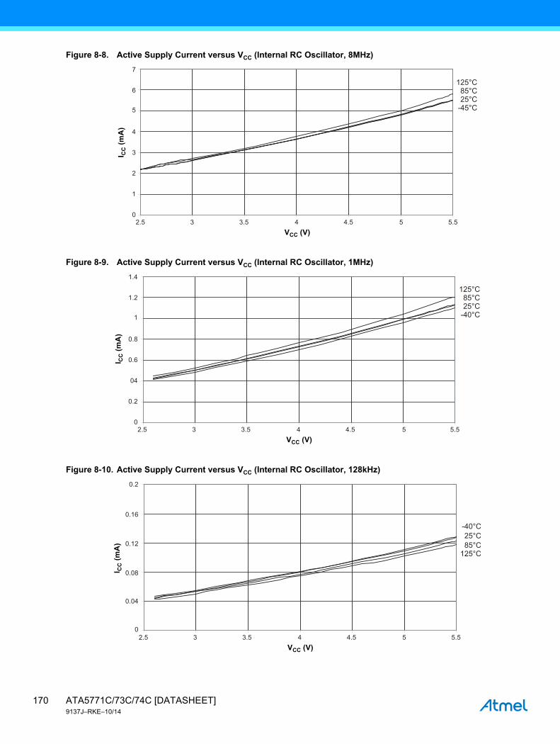
Figure 8-8. Active Supply Current versus VCC (Internal RC Oscillator, 8MHz)
Figure 8-9. Active Supply Current versus VCC (Internal RC Oscillator, 1MHz)
Figure 8-10. Active Supply Current versus VCC (Internal RC Oscillator, 128kHz)
2.5 3 3.5 4 4.5 5 5.5
5
6
7
4
3
2
1
0
I CC (m
A)
VCC (V)
125°C85°C25°C
-45°C
1
1.2
1.4
0.8
0.6
04
0.2
0
I CC (m
A)
2.5 3 3.5 4 4.5 5 5.5VCC (V)
125°C85°C25°C
-40°C
0.2
0.16
0.12
0.08
0.04
0
I CC (m
A)
2.5 3 3.5 4 4.5 5 5.5VCC (V)
-40°C25°C85°C
125°C
ATA5771C/73C/74C [DATASHEET]9137J–RKE–10/14
170

8.3.8.2 Idle Supply Current
Figure 8-11. Idle Supply Current versus VCC (Internal RC Oscillator, 8MHz)
Figure 8-12. Idle Supply Current versus VCC (Internal RC Oscillator, 1MHz)
1.0
1.2
0.8
0.6
0.4
0.2
0
I CC (m
A)
2.5 3 3.5 4 4.5 5 5.5VCC (V)
125°C85°C25°C
-40°C1.4
1.6
1.8
2.0
2.5 3 3.5 4 4.5 5 5.5VCC (V)
125°C85°C25°C
-40°C0.25
0.3
0.2
0.15
0.1
0.05
0
I CC (m
A)
0.35
171ATA5771C/73C/74C [DATASHEET]9137J–RKE–10/14

Figure 8-13. Idle Supply Current versus VCC (Internal RC Oscillator, 128kHz)
8.3.8.3 Supply Current of IO modules
The tables and formulas below can be used to calculate the additional current consumption for the different I/O modules in active and idle mode. The enabling or disabling of the I/O modules are controlled by the power reduction register. See Section 4.10.7 “Power Reduction Register” on page 36 for details.
8.3.8.4 Power-down Supply Current
Figure 8-14. Power-down Supply Current versus VCC (Watchdog Timer Disabled)
2.5 3 3.5 4 4.5 5 5.5VCC (V)
125°C85°C25°C
-40°C0.025
0.03
0.02
0.015
0.01
0.005
0
I CC (m
A)
0.035
Table 8-9. Additional Current Consumption for the Different I/O Modules (Absolute Values)
PRR Bit Typical Numbers
VCC = 2V, F = 1MHz VCC = 3V, F = 4MHz
PRTIM1 6.6µA 26µA
PRTIM0 8.7µA 35µA
PRUSI 5.5µA 22µA
PRADC 22µA 87µA
2.5 3 3.5 4 4.5 5 5.5VCC (V)
125°C
85°C
25°C-45°C
2.5
3
2
1.5
1
0.5
0
I CC (µ
A)
3.5
4
5.5
5
ATA5771C/73C/74C [DATASHEET]9137J–RKE–10/14
172

Figure 8-15. Power-down Supply Current versus VCC (Watchdog Timer Enabled)
8.3.8.5 Pin Pull-up
Figure 8-16. I/O Pin Pull-up Resistor Current versus Input Voltage (VCC = 2.7V)
2.5 3 3.5 4 4.5 5 5.5VCC (V)
5
6
4
3
2
1
0
I CC (µ
A)
7
8
9
10
125°C-45°C85°C25°C
0 0.5 1 1.5 2 2.5 3VOP (V)
-45°C25°C85°C
125°C
50
60
40
30
20
10
0
I OP
(µA
)
70
80
90
173ATA5771C/73C/74C [DATASHEET]9137J–RKE–10/14

Figure 8-17. Reset Pull-up Resistor Current versus Reset Pin Voltage (VCC = 2.7V)
8.3.8.6 Pin Driver Strength
Figure 8-18. I/O Pin Output Voltage versus Sink Current (VCC = 3V)
Figure 8-19. I/O Pin Output Voltage versus Source Current (VCC = 3V)
-40°C
125°C
0 0.5 1 1.5 2 2.5 3VRESET (V)
50
60
40
30
20
10
0
I RES
ET (µ
A)
0.05
0.06
0.04
0.03
0.02
0.01
0
V OL
(V)
0 2 4 6 8 10 12 14 16 18 20IOL (mA)
125°C
85°C25°C
-40°C
3.5
3
2.5
2
1.5
V OH (V
)
0 2 4 6 8 10 12 14 16 18 20IOH (mA)
-45°C
25°C85°C
125°C
ATA5771C/73C/74C [DATASHEET]9137J–RKE–10/14
174

8.3.8.7 Pin Threshold and Hysteresis
Figure 8-20. I/O Pin Input Threshold Voltage versus VCC (VIH, IO Pin Read as ‘1’)
Figure 8-21. I/O Pin Input threshold Voltage versus VCC (VIL, IO Pin Read as ‘0’)
2.5 3 3.5 4 4.5 5 5.5VCC (V)
125°C85°C25°C
-40°C2.5
3
2
1.5
1
0.5
0
Thre
shol
d (V
)
3.5
2.5 3 3.5 4 4.5 5 5.5VCC (V)
125°C85°C25°C
-40°C
2.5
2
1.5
1
0.5
0
Thre
shol
d (V
)
175ATA5771C/73C/74C [DATASHEET]9137J–RKE–10/14

Figure 8-22. I/O Pin Input Hysteresis versus VCC
Figure 8-23. Reset Input Threshold Voltage versus VCC (VIH, IO Pin Threshold as ‘1’)
Figure 8-24. Reset Input Threshold Voltage versus VCC (VIL, IO pin Read as ‘0’)
2.5 3 3.5 4 4.5 5 5.5VCC (V)
125°C85°C
-20°C-40°C
0.25
0.3
0.2
0.15
0.1
0.05
0
Inpu
t Hys
tere
sis
(mV) 0.35
0.4
0.45
0.5
2.5 3 3.5 4 4.5 5 5.5VCC (V)
125°C85°C25°C
-40°C2.5
3
2
1.5
1
0.5
0
Thre
shol
d (V
)
2.5 3 3.5 4 4.5 5 5.5VCC (V)
125°C85°C25°C
-45°C
2.5
3
2
1.5
1
0.5
0
Thre
shol
d (V
)
ATA5771C/73C/74C [DATASHEET]9137J–RKE–10/14
176

Figure 8-25. Reset Pin Input Hysteresis versus VCC
8.3.8.8 BOD Threshold and Analog Comparator Offset
Figure 8-26. BOD Threshold versus Temperature (BODLEVEL is 2.7V)
Figure 8-27. BOD Threshold versus Temperature (BODLEVEL is 1.8V)
2.5 3 3.5 4 4.5 5 5.5VCC (V)
125°C85°C
25°C
-40°C0.5
0.6
0.4
0.3
0.2
0.1
0
Inpu
t Hys
tere
sis
(mV) 0.7
0.8
0.9
1
2.74
2.76
2.78
2.72
2.7
2.68
2.66
2.64
Thre
shol
de (V
)
-40 -30 -20 -10 0 10 20 30 40 50 60 70 80
1
0
90 100 110 120
Temperature (°C)
1.83
1.84
1.85
1.82
1.81
1.8
1.79
1.78
Thre
shol
de (V
)
1
0
-40 -30 -20 -10 0 10 20 30 40 50 60 70 80 90 100 110 120
Temperature (°C)
177ATA5771C/73C/74C [DATASHEET]9137J–RKE–10/14

8.3.8.9 Internal Oscillator Speed
Figure 8-28. Watchdog Oscillator Frequency versus VCC
Figure 8-29. Calibrated 8MHz RC Oscillator Frequency versus VCC
114
116
118
120
122
124
112
110
108
106
104
F RC (k
Hz)
2.5 3 3.5 4 4.5 5 5.5VCC (V)
125°C
85°C
25°C
-40°C
8.5
9
8
7.5
7
6.5
6
F RC (M
Hz)
2.5 3 3.5 4 4.5 5 5.5VCC (V)
125°C85°C25°C
-40°C
ATA5771C/73C/74C [DATASHEET]9137J–RKE–10/14
178
Figure 8-30. Calibrated 8MHz RC oscillator Frequency versus Temperature
Figure 8-31. Calibrated 8MHz RC Oscillator Frequency versus OSCCAL Value
8.2
8.3
8.4
8.1
8
7.9
7.8
7.7
5V3V
-40 -30 -20 -10 0 10 20 30 40 50 60 70 80 90 100 110 120
Temperature (°C)
F RC (M
Hz)
0 16 32 48 64 80 96 112 128 144 160 176 192 208 224 240
OSCCAL (X1)
12
14
16
10
8
6
4
2
0
F RC (M
Hz)
125°C85°C25°C
-40°C
179ATA5771C/73C/74C [DATASHEET]9137J–RKE–10/14

8.3.8.10 Current Consumption of Peripheral Units
Figure 8-32. ADC Current versus VCC
Figure 8-33. Analog Comparator Current versus VCC
600
700
500
400
300
200
100
0
I CC (µ
A)
2.5 3 3.5 4 4.5 5 5.5VCC (V)
125°C85°C25°C
-40°C
90
100
80
70
60
50
40
30
20
10
0
I CC (µ
A)
2.5 3 3.5 4 4.5 5 5.5VCC (V)
-40°C25°C85°C
125°C
ATA5771C/73C/74C [DATASHEET]9137J–RKE–10/14
180

Figure 8-34. Programming Current versus VCC
Figure 8-35. Brownout Detector Current versus VCC
Figure 8-36. Watchdog Timer Current versus VCC
10000
12000
8000
6000
4000
2000
0
I CC (µ
A)
2.5 3.5 4.5 5.5VCC (V)
25°C
10
12
14
16
8
6
4
2
0
I CC (µ
A)
1.5 1.6 1.7 1.8 1.9 2 2.1 2.2 2.3 2.4 2.5VCC (V)
125°C
85°C
25°C
-40°C
25
30
20
15
10
5
0
I CC (µ
A)
2.5 3 3.5 4 4.5 5 5.5VCC (V)
-40°C25°C85°C
125°C
181ATA5771C/73C/74C [DATASHEET]9137J–RKE–10/14

8.3.8.11 Current Consumption in Reset and Reset Pulse Width
Figure 8-37. Reset Supply Current versus VCC (0.1 - 1.0MHz, excluding Current Through the Reset Pull-up)
Figure 8-38. Reset Supply Current versus VCC (1 - 20MHz, Excluding Current Through the Reset Pull-up)
Figure 8-39. Minimum Reset Pulse Width versus VCC
0.18
0.20
0.16
0.14
0.12
0.10
0.08
0.06
0.04
0.02
0
I CC (m
A)
0 0.1 0.2 0.3 0.4 0.5 0.6 0.7 0.8 0.9 1Frequency (MHz)
5.5V5.0V
4.5V
3.3V3.0V2.7V
3
2.5
2
1.5
1
0.5
0
I CC (m
A)
0 2 4 6 8 10 12 14 16 18 20Frequency (MHz)
5.5V
5.0V
4.5V
3.3V3.6V
3.0V2.7V
1000
1200
800
600
400
200
0
Puls
e W
idth
(ns)
2.5 3 3.5 4 4.5 5 5.5VCC (V)
125°C85°C25°C
-40°C
ATA5771C/73C/74C [DATASHEET]9137J–RKE–10/14
182

9. Appendix
9.1 Register Summary
Address Name Bit 7 Bit 6 Bit 5 Bit 4 Bit 3 Bit 2 Bit 1 Bit 0 Page
0x3F (0x5F) SREG I T H S V N Z C 16
0x3E (0x5E) SPH – – – – – – SP9 SP8 18
0x3D (0x5D) SPL SP7 SP6 SP5 SP4 SP3 SP2 SP1 SP0 18
0x3C (0x5C) OCR0B Timer/Counter0 – Output Compare Register B 79
0x3B (0x5B) GIMSK – INT0 PCIE1 PCIE0 – – – – 50
0x3A (0x5A GIFR – INTF0 PCIF1 PCIF0 – – – – 50
0x39 (0x59) TIMSK0 – – – – – OCIE0B OCIE0A TOIE0 79
0x38 (0x58) TIFR0 – – – – OCF0B OCF0A TOV0 80
0x37 (0x57) SPMCSR – – – CTPB RFLB PGWRT PGERS SPMEN 141
0x36 (0x56) OCR0A Timer/Counter0 – Output Compare Register A 79
0x35 (0x55) MCUCR BODS PUD SE SM1 SM0 BODSE ISC01 ISC00 49
0x34 (0x54) MCUSR – – – – WDRF BORF EXTRF PORF 44
0x33 (0x53) TCCR0B FOC0A FOC0B – – WGM02 CS02 CS01 CS00 78
0x32 (0x52) TCNT0 Timer/Counter0 79
0x31 (0x51) OSCCAL CAL7 CAL6 CAL5 CAL4 CAL3 CAL2 CAL1 CAL0 33
0x30 (0x50) TCCR0A COM0A1 COM0A0 COM0B1 COM0B0 – – WGM01 WGM00 75
0x2F (0x4F) TCCR1A COM1A1 COM1A0 COM1B1 COM1B0 – – WGM11 WGM10 99
0x2E (0x4E) TCCR1B ICNC1 ICES1 – WGM13 WGM12 CS12 CS11 CS10 101
0x2D (0x4D) TCNT1H Timer/Counter1 – Counter Register High Byte 102
0x2C (0x4C) TCNT1L Timer/Counter1 – Counter Register Low Byte 102
0x2B (0x4B) OCR1AH Timer/Counter1 – Compare Register A High Byte 102
0x2A (0x4A) OCR1AL Timer/Counter1 – Compare Register A Low Byte 102
0x29 (0x49) OCR1BH Timer/Counter1 – Compare Register B High Byte 103
0x28 (0x48) OCR1BL Timer/Counter1 – Compare Register B Low Byte 103
0x27 (0x47) DWDR DWDR[7:0] 138
0x26 (0x46) CLKPR CLKPCE – – – CLKPS3 CLKPS2 CLKPS1 CLKPS0 33
0x25 (0x45) ICR1H Timer/Counter1 - Input Capture Register High Byte 103
0x24 (0x44) ICR1L Timer/Counter1 - Input Capture Register Low Byte 103
0x23 (0x43) GTCCR TSM – – – – – – PSR10 106
0x22 (0x42) TCCR1C FOC1A FOC1B – – – – – – 102
0x21 (0x41) WDTCSR WDIF WDIE WDP3 WDCE WDE WDP2 WDP1 WDP0 44
0x20 (0x40) PCMSK1 – – – – PCINT11 PCINT10 PCINT9 PCINT8 51
0x1F (0x3F) EEARH – – – – – – – EEAR8 25
0x1E (0x3E) EEARL EEAR7 EEAR6 EEAR5 EEAR4 EEAR3 EEAR2 EEAR1 EEAR0 25
Notes: 1. For compatibility with future devices, reserved bits should be written to zero if accessed. Reserved I/O memory addresses should never be written.
2. I/O Registers within the address range 0x00 - 0x1F are directly bit-accessible using the SBI and CBI instructions. In these registers, the value of single bits can be checked by using the SBIS and SBIC instructions.
3. Some of the Status Flags are cleared by writing a logical one to them. Note that, unlike most other AVR®s, the CBI and SBI instructions will only operation the specified bit, and can therefore be used on registers containing such Status Flags. The CBI and SBI instructions work with registers 0x00 to 0x1F only
183ATA5771C/73C/74C [DATASHEET]9137J–RKE–10/14

0x1D (0x3D) EEDR EEPROM Data Register 25
0x1C (0x3C) EECR – – EEPM1 EEPM0 EERIE EEMPE EEPE EERE 25
0x1B (0x3B) PORTA PORTA7 PORTA6 PORTA5 PORTA4 PORTA3 PORTA2 PORTA1 PORTA0 64
0x1A (0x3A) DDRA DDA7 DDA6 DDA5 DDA4 DDA3 DDA2 DDA1 DDA0 64
0x19 (0x39) PINA PINA7 PINA6 PINA5 PINA4 PINA3 PINA2 PINA1 PINA0 65
0x18 (0x38) PORTB – – – – PORTB3 PORTB2 PORTB1 PORTB0 65
0x17 (0x37) DDRB – – – – DDB3 DDB2 DDB1 DDB0 65
0x16 (0x36) PINB – – – – PINB3 PINB2 PINB1 PINB0 65
0x15 (0x35) GPIOR2 General Purpose I/O Register 2 26
0x14 (0x34) GPIOR1 General Purpose I/O Register 1 27
0x13 (0x33) GPIOR0 General Purpose I/O Register 0 27
0x12 (0x32) PCMSK0 PCINT7 PCINT6 PCINT5 PCINT4 PCINT3 PCINT2 PCINT1 PCINT0 51
0x11 (0x31)) Reserved –
0x10 (0x30) USIBR USI Buffer Register 113
0x0F (0x2F) USIDR USI Data Register 113
0x0E (0x2E) USISR USISIF USIOIF USIPF USIDC USICNT3 USICNT2 USICNT1 USICNT0 114
0x0D (0x2D) USICR USISIE USIOIE USIWM1 USIWM0 USICS1 USICS0 USICLK USITC 115
0x0C (0x2C) TIMSK1 – – ICIE1 – – OCIE1B OCIE1A TOIE1 103
0x0B (0x2B) TIFR1 – – ICF1 – – OCF1B OCF1A TOV1 104
0x0A (0x2A) Reserved –
0x09 (0x29) Reserved –
0x08 (0x28) ACSR ACD ACBG ACO ACI ACIE ACIC ACIS1 ACIS0 118
0x07 (0x27) ADMUX REFS1 REFS0 MUX5 MUX4 MUX3 MUX2 MUX1 MUX0 131
0x06 (0x26) ADCSRA ADEN ADSC ADATE ADIF ADIE ADPS2 ADPS1 ADPS0 134
0x05 (0x25) ADCH ADC Data Register High Byte 135
0x04 (0x24) ADCL ADC Data Register Low Byte 135
0x03 (0x23) ADCSRB BIN ACME – ADLAR – ADTS2 ADTS1 ADTS0 118
0x02 (0x22) Reserved –
0x01 (0x21) DIDR0 ADC7D ADC6D ADC5D ADC4D ADC3D ADC2D ADC1D ADC0D 119,136
0x00 (0x20) PRR – – – – PRTIM1 PRTIM0 PRUSI PRADC 38
9.1 Register Summary
Address Name Bit 7 Bit 6 Bit 5 Bit 4 Bit 3 Bit 2 Bit 1 Bit 0 Page
Notes: 1. For compatibility with future devices, reserved bits should be written to zero if accessed. Reserved I/O memory addresses should never be written.
2. I/O Registers within the address range 0x00 - 0x1F are directly bit-accessible using the SBI and CBI instructions. In these registers, the value of single bits can be checked by using the SBIS and SBIC instructions.
3. Some of the Status Flags are cleared by writing a logical one to them. Note that, unlike most other AVR®s, the CBI and SBI instructions will only operation the specified bit, and can therefore be used on registers containing such Status Flags. The CBI and SBI instructions work with registers 0x00 to 0x1F only
ATA5771C/73C/74C [DATASHEET]9137J–RKE–10/14
184
9.2 Instruction Set Summary
Mnemonics Operands Description Operation Flags #Clocks
Arithmetic and Logic Instructions
ADD Rd, Rr Add two registers Rd ← Rd + Rr Z,C,N,V,H 1
ADC Rd, Rr Add with carry two registers Rd ← Rd + Rr + C Z,C,N,V,H 1
ADIW Rdl,K Add immediate to word Rdh:Rdl ← Rdh:Rdl + K Z,C,N,V,S 2
SUB Rd, Rr Subtract two registers Rd ← Rd – Rr Z,C,N,V,H 1
SUBI Rd, K Subtract constant from register Rd ← Rd – K Z,C,N,V,H 1
SBC Rd, Rr Subtract with carry two registers Rd ← Rd – Rr – C Z,C,N,V,H 1
SBCI Rd, K Subtract with carry constant from reg. Rd ← Rd – K – C Z,C,N,V,H 1
SBIW Rdl,K Subtract immediate from word Rdh:Rdl ← Rdh:Rdl – K Z,C,N,V,S 2
AND Rd, Rr Logical AND registers Rd ← Rd × Rr Z,N,V 1
ANDI Rd, K Logical AND register and constant Rd ← Rd × K Z,N,V 1
OR Rd, Rr Logical OR registers Rd ← Rd v Rr Z,N,V 1
ORI Rd, K Logical OR register and constant Rd ← Rd v K Z,N,V 1
EOR Rd, Rr Exclusive OR registers Rd ← Rd ⊕ Rr Z,N,V 1
COM Rd One’s complement Rd ← 0xFF – Rd Z,C,N,V 1
NEG Rd Two’s complement Rd ← 0x00 – Rd Z,C,N,V,H 1
SBR Rd,K Set Bit(s) in register Rd ← Rd v K Z,N,V 1
CBR Rd,K Clear Bit(s) in register Rd ← Rd × (0xFF - K) Z,N,V 1
INC Rd Increment Rd ← Rd + 1 Z,N,V 1
DEC Rd Decrement Rd ← Rd – 1 Z,N,V 1
TST Rd Test for zero or minus Rd ← Rd × Rd Z,N,V 1
CLR Rd Clear register Rd ← Rd ⊕ Rd Z,N,V 1
SER Rd Set register Rd ← 0xFF None 1
Branch Instructions
RJMP k Relative jump PC ← PC + k + 1 None 2
IJMP Indirect jump to (Z) PC ← Z None 2
RCALL k Relative subroutine call PC ← PC + k + 1 None 3
ICALL Indirect call to (Z) PC ← Z None 3
RET Subroutine return PC ← STACK None 4
RETI Interrupt return PC ← STACK I 4
CPSE Rd,Rr Compare, skip if equal if (Rd = Rr) PC ← PC + 2 or 3 None 1/2/3
CP Rd,Rr Compare Rd − Rr Z, N,V,C,H 1
CPC Rd,Rr Compare with carry Rd − Rr − C Z, N,V,C,H 1
CPI Rd,K Compare register with immediate Rd − K Z, N,V,C,H 1
SBRC Rr, b Skip if bit in register cleared if (Rr(b)=0) PC ← PC + 2 or 3 None 1/2/3
SBRS Rr, b Skip if bit in register is set if (Rr(b)=1) PC ← PC + 2 or 3 None 1/2/3
SBIC P, b Skip if bit in I/O register cleared if (P(b)=0) PC ← PC + 2 or 3 None 1/2/3
SBIS P, b Skip if bit in I/O register is set if (P(b)=1) PC ← PC + 2 or 3 None 1/2/3
BRBS s, k Branch if status flag setif (SREG(s) = 1) then PC ←
PC + k + 1None 1/2
BRBC s, k Branch if status flag clearedif (SREG(s) = 0) then PC ←
PC + k + 1None 1/2
BREQ k Branch if equal if (Z = 1) then PC ← PC + k + 1 None 1/2
BRNE k Branch if not equal if (Z = 0) then PC ← PC + k + 1 None 1/2
BRCS k Branch if carry set if (C = 1) then PC ← PC + k + 1 None 1/2
185ATA5771C/73C/74C [DATASHEET]9137J–RKE–10/14

BRCC k Branch if carry cleared if (C = 0) then PC ← PC + k + 1 None 1/2
BRSH k Branch if same or higher if (C = 0) then PC ← PC + k + 1 None 1/2
BRLO k Branch if lower if (C = 1) then PC ← PC + k + 1 None 1/2
BRMI k Branch if minus if (N = 1) then PC ← PC + k + 1 None 1/2
BRPL k Branch if plus if (N = 0) then PC ← PC + k + 1 None 1/2
BRGE k Branch if greater or equal, signed if (N ⊕ V= 0) then PC ← PC + k + 1 None 1/2
BRLT k Branch if less than zero, signed if (N ⊕ V= 1) then PC ← PC + k + 1 None 1/2
BRHS k Branch if half carry flag set if (H = 1) then PC ← PC + k + 1 None 1/2
BRHC k Branch if half carry flag cleared if (H = 0) then PC ← PC + k + 1 None 1/2
BRTS k Branch if T flag set if (T = 1) then PC ← PC + k + 1 None 1/2
BRTC k Branch if T flag cleared if (T = 0) then PC ← PC + k + 1 None 1/2
BRVS k Branch if overflow flag is set if (V = 1) then PC ← PC + k + 1 None 1/2
BRVC k Branch if overflow flag is cleared if (V = 0) then PC ← PC + k + 1 None 1/2
BRIE k Branch if interrupt enabled if (I = 1) then PC ← PC + k + 1 None 1/2
BRID k Branch if interrupt disabled if (I = 0) then PC ← PC + k + 1 None 1/2
Bit and Bit-test Instructions
SBI P,b Set bit in I/O register I/O(P,b) ← 1 None 2
CBI P,b Clear bit in I/O register I/O(P,b) ← 0 None 2
LSL Rd Logical shift left Rd(n+1) ← Rd(n), Rd(0) ← 0 Z,C,N,V 1
LSR Rd Logical shift right Rd(n) ← Rd(n+1), Rd(7) ← 0 Z,C,N,V 1
ROL Rd Rotate left through carryRd(0) ← C,Rd(n+1) ← Rd(n),C
←Rd(7)Z,C,N,V 1
ROR Rd Rotate right through carryRd(7) ← C,Rd(n) ← Rd(n+1),C ←
Rd(0)Z,C,N,V 1
ASR Rd Arithmetic shift right Rd(n) ← Rd(n+1), n=0..6 Z,C,N,V 1
SWAP Rd Swap nibblesRd(3..0) ← Rd(7..4),Rd(7..4) ←
Rd(3..0)None 1
BSET s Flag set SREG(s) ← 1 SREG(s) 1
BCLR s Flag clear SREG(s) ← 0 SREG(s) 1
BST Rr, b Bit store from register to T T ← Rr(b) T 1
BLD Rd, b Bit load from T to register Rd(b) ← T None 1
SEC Set carry C ← 1 C 1
CLC Clear carry C ← 0 C 1
SEN Set negative flag N ← 1 N 1
CLN Clear negative flag N ← 0 N 1
SEZ Set zero flag Z ← 1 Z 1
CLZ Clear zero flag Z ← 0 Z 1
SEI Global interrupt enable I ← 1 I 1
CLI Global interrupt disable I ← 0 I 1
SES Set signed test flag S ← 1 S 1
CLS Clear signed test flag S ← 0 S 1
SEV Set twos complement overflow. V ← 1 V 1
CLV Clear twos complement overflow V ← 0 V 1
SET Set T in SREG T ← 1 T 1
CLT Clear T in SREG T ← 0 T 1
SEH Set half carry flag in SREG H ← 1 H 1
9.2 Instruction Set Summary (Continued)
Mnemonics Operands Description Operation Flags #Clocks
ATA5771C/73C/74C [DATASHEET]9137J–RKE–10/14
186

CLH Clear Half Carry Flag in SREG H ← 0 H 1
Data Transfer Instructions
MOV Rd, Rr Move between registers Rd ← Rr None 1
MOVW Rd, Rr Copy register word Rd+1:Rd ← Rr+1:Rr None 1
LDI Rd, K Load immediate Rd ← K None 1
LD Rd, X Load indirect Rd ← (X) None 2
LD Rd, X+ Load indirect and post-inc. Rd ← (X), X ← X + 1 None 2
LD Rd, - X Load indirect and pre-dec. X ← X - 1, Rd ← (X) None 2
LD Rd, Y Load indirect Rd ← (Y) None 2
LD Rd, Y+ Load indirect and post-inc. Rd ← (Y), Y ← Y + 1 None 2
LD Rd, - Y Load indirect and pre-dec. Y ← Y - 1, Rd ← (Y) None 2
LDD Rd,Y+q Load indirect with displacement Rd ← (Y + q) None 2
LD Rd, Z Load indirect Rd ← (Z) None 2
LD Rd, Z+ Load indirect and post-inc. Rd ← (Z), Z ← Z+1 None 2
LD Rd, -Z Load indirect and pre-dec. Z ← Z - 1, Rd ← (Z) None 2
LDD Rd, Z+q Load indirect with displacement Rd ← (Z + q) None 2
LDS Rd, k Load direct from SRAM Rd ← (k) None 2
ST X, Rr Store indirect (X) ← Rr None 2
ST X+, Rr Store indirect and post-inc. (X) ← Rr, X ← X + 1 None 2
ST - X, Rr Store indirect and pre-dec. X ← X - 1, (X) ← Rr None 2
ST Y, Rr Store indirect (Y) ← Rr None 2
ST Y+, Rr Store indirect and post-inc. (Y) ← Rr, Y ← Y + 1 None 2
ST - Y, Rr Store indirect and pre-dec. Y ← Y - 1, (Y) ← Rr None 2
STD Y+q,Rr Store indirect with displacement (Y + q) ← Rr None 2
ST Z, Rr Store indirect (Z) ← Rr None 2
ST Z+, Rr Store indirect and post-inc. (Z) ← Rr, Z ← Z + 1 None 2
ST -Z, Rr Store indirect and pre-dec. Z ← Z - 1, (Z) ← Rr None 2
STD Z+q,Rr Store indirect with displacement (Z + q) ← Rr None 2
STS k, Rr Store direct to SRAM (k) ← Rr None 2
LPM Load program memory R0 ← (Z) None 3
LPM Rd, Z Load program memory Rd ← (Z) None 3
LPM Rd, Z+ Load program memory and post-inc Rd ← (Z), Z ← Z+1 None 3
SPM Store program memory (z) ← R1:R0 None
IN Rd, P In port Rd ← P None 1
OUT P, Rr Out port P ← Rr None 1
PUSH Rr Push register on stack STACK ← Rr None 2
POP Rd Pop register from stack Rd ← STACK None 2
MCU Control Instructions
NOP No operation None 1
SLEEP Sleep(see specific descr. for sleep
function)None 1
WDR Watchdog reset (see specific descr. for WDR/timer) None 1
BREAK Break For on-chip debug only None N/A
9.2 Instruction Set Summary (Continued)
Mnemonics Operands Description Operation Flags #Clocks
187ATA5771C/73C/74C [DATASHEET]9137J–RKE–10/14

11. Package Information
10. Ordering Information
Extended Type Number Package Remarks
ATA5771C-PXQW-1 QFN24 5mm x 5mm Microcontroller with UHF Tx for 868MHz to 928MHz, 6K, taped and reeled
ATA5773C-PXQW-1 QFN24 5mm x 5mm Microcontroller with UHF Tx for 310MHz to 350MHz, 6K, taped and reeled
ATA5774C-PXQW-1 QFN24 5mm x 5mm Microcontroller with UHF Tx for 429MHz to 439MHz, 6K, taped and reeled
Package Drawing Contact:[email protected]
GPC DRAWING NO. REV. TITLE
6.543-5132.02-4 1
10/18/13
Package: VQFN_5x5_24LExposed pad 3.6x3.6
COMMON DIMENSIONS(Unit of Measure = mm)
MIN NOM NOTEMAXSymbol
Dimensions in mm
specificationsaccording to DINtechnical drawings
0.035 0.050.0A1
5 5.14.9E
0.25 0.30.2b0.65e
0.4 0.450.35L3.6 3.73.5E2
3.6 3.73.5D25 5.14.9D
0.21 0.260.16A3
0.85 0.90.8A
Top ViewD
24
1
6
PIN 1 ID
E
Side View A3
A
A1
b
LZ 10:1
Bottom View
e
D2
24 19
7
1
612
13
18
E2
Z
ATA5771C/73C/74C [DATASHEET]9137J–RKE–10/14
188
12. Revision History
Please note that the following page numbers referred to in this section refer to the specific revision mentioned, not to this document.
Revision No. History
9137J-RKE-10/14• Section 10 “Ordering Information” on page 188 updated
• Section 11 “Package Information” on page 188 updated
9137I-RKE-08/14 • Put datasheet in the latest template
9137H-RKE-10/13 • Section 10 “Ordering Information” on page 189 updated
9137G-RKE-09/12 • Section 10 “Ordering Information” on page 218 updated
9137F-RKE-05/11
• Table 2-1 “Pin Description” on page 4 changed
• Section 4.10.6 “Software BOD Disable” on page 42 added
• Section 4.10.8.3 “Brown-out Detector” on page 43 changed
• Section 4.10.9.1 “MCUCR – MCU Control Register” on pages 44 to 45 changed
9137E-RKE-12/10
• Section 8.1 “The General Current Consumption Characteristics for Key Fob Application” on page 186 changed
• Section 8.2 “RF Transmitter Block” on pages 186 to 187 changed
• Section 8.3 “Microcontroller Block” on pages 188 to 212 changed
9137D-RKE-09/10
• All pages: ATtiny24 and ATtiny84 deleted
• All pages: Flash size 2k and 8k deleted
• Figures 4-7 and 4-8 changed
• Text under headings 4.2, 4.8.1, 4.8.2, 4.8.3, 4.8.5.1 and 4.8.5.2 changed
• Section 8.1 “The General Current Consumption Characteristics for Key Fob Application” on page 186 changed
• Table 8-1 “Calibration Accuracy of Internal RC Oscillator” on page 189 changed
• Table 8-4 “BODLEVEL Fuse Coding” on page 190 changed
189ATA5771C/73C/74C [DATASHEET]9137J–RKE–10/14

XX X XX XAtmel Corporation 1600 Technology Drive, San Jose, CA 95110 USA T: (+1)(408) 441.0311 F: (+1)(408) 436.4200 | www.atmel.com
© 2014 Atmel Corporation. / Rev.: 9137J–RKE–10/14
Atmel®, Atmel logo and combinations thereof, Enabling Unlimited Possibilities®, AVR®, AVR Studio®, and others are registered trademarks or trademarks of Atmel Corporation in U.S. and other countries. Other terms and product names may be trademarks of others.
DISCLAIMER: The information in this document is provided in connection with Atmel products. No license, express or implied, by estoppel or otherwise, to any intellectual property rightis granted by this document or in connection with the sale of Atmel products. EXCEPT AS SET FORTH IN THE ATMEL TERMS AND CONDITIONS OF SALES LOCATED ON THEATMEL WEBSITE, ATMEL ASSUMES NO LIABILITY WHATSOEVER AND DISCLAIMS ANY EXPRESS, IMPLIED OR STATUTORY WARRANTY RELATING TO ITS PRODUCTSINCLUDING, BUT NOT LIMITED TO, THE IMPLIED WARRANTY OF MERCHANTABILITY, FITNESS FOR A PARTICULAR PURPOSE, OR NON-INFRINGEMENT. IN NO EVENTSHALL ATMEL BE LIABLE FOR ANY DIRECT, INDIRECT, CONSEQUENTIAL, PUNITIVE, SPECIAL OR INCIDENTAL DAMAGES (INCLUDING, WITHOUT LIMITATION, DAMAGESFOR LOSS AND PROFITS, BUSINESS INTERRUPTION, OR LOSS OF INFORMATION) ARISING OUT OF THE USE OR INABILITY TO USE THIS DOCUMENT, EVEN IF ATMEL HASBEEN ADVISED OF THE POSSIBILITY OF SUCH DAMAGES. Atmel makes no representations or warranties with respect to the accuracy or completeness of the contents of thisdocument and reserves the right to make changes to specifications and products descriptions at any time without notice. Atmel does not make any commitment to update the informationcontained herein. Unless specifically provided otherwise, Atmel products are not suitable for, and shall not be used in, automotive applications. Atmel products are not intended,authorized, or warranted for use as components in applications intended to support or sustain life.
SAFETY-CRITICAL, MILITARY, AND AUTOMOTIVE APPLICATIONS DISCLAIMER: Atmel products are not designed for and will not be used in connection with any applications wherethe failure of such products would reasonably be expected to result in significant personal injury or death (“Safety-Critical Applications”) without an Atmel officer's specific writtenconsent. Safety-Critical Applications include, without limitation, life support devices and systems, equipment or systems for the operation of nuclear facilities and weapons systems.Atmel products are not designed nor intended for use in military or aerospace applications or environments unless specifically designated by Atmel as military-grade. Atmel products arenot designed nor intended for use in automotive applications unless specifically designated by Atmel as automotive-grade.