asm-2 manual - elby designs · from electronotes and has the following features:- • the frequency...
TRANSCRIPT

ASM-2 Manual
Elby Designs - Laurie Biddulph 9 Follan Close, Kariong, NSW 2250, Australia
[email protected] http://www.elby-designs.com 1 of 24
ASM-2 Manual
February 20th 2013
Please note that this document is still currently under revision and we apologise for any errors or omissions.
Readers should feel free to email any comments to me at the address given below.
ASM-2 Manual
Elby Designs - Laurie Biddulph 9 Follan Close, Kariong, NSW 2250, Australia
[email protected] http://www.elby-designs.com 2 of 24
***** NOTICE *****
This documentation is still currently in revision. It is a copy of the original ASM-1 documentation that I am currently updating to reflect the changes introduced with the release of the ASM-2. The bulk of this documentation is still fully valid as most of the ASM-2 circuits are either the same as the original ASM-1 circuits or contain enhancements over the original ASM-1 circuit. As such readers can safely refer to this document for most information relating to the various ASM-2 circuits. Component designators in some cases may be incorrect and some of the new features of the ASM-2 will not have been documented so far. I do apologise for any inconvenience that this may cause. Please feel free to email with any enquiries or concerns you may have. Readers should regular check my website for updates to this and other related documentation which I am currently working on.
ASM-2 Manual
Elby Designs - Laurie Biddulph 9 Follan Close, Kariong, NSW 2250, Australia
[email protected] http://www.elby-designs.com 3 of 24
Introduction The ASM-2 combines a set of fairly traditional analog synthesiser modules on to a single printed circuit board. The modules are:- • Two Voltage Controlled Oscillators (VCO's) – sawtooth, variable rectangular (pulse-
width modulated), triangle and psuedo-sine outputs • One Voltage Controlled State-Variable Filter (VCF) – low-pass, band-pass, high-pass
and notch outputs • One Voltage Controller Transistor-Ladder Filter • Two 2 Voltage Controlled Amplifiers (VCA's) - Linear response • Two ADSR Envelope Generators - exponential curves • Two Voltage Controlled Low Frequency Oscillators (VCLFO) - triangle and square
outputs • One Noise Source - white, variable coloured and random outputs • One CV Glide Buffer - exponential glide • One Sample & Hold circuit • One Ring Modulator • Regulated dual-rail power supply (+15, 0V, -15V at 400mA) Most of these modules are, in the most, minor variations to the Electronotes EN76 series, and have been incorporated with the relevant owners permission. These circuit sections can be considered "modules" as they are not interconnected in any way on the circuit board other than by power and ground busses. Therefore the builder has the freedom to use the ASM-2 in any type of design desired, from a small hard-wired system to a fully patchable semi-modular system. In addition to the ASM-2 board, most builders will need to supply the following additional circuit modules:- • Case and front panel. The ASM-2 should be housed in a suitable enclosure to ensure
that the unit does not get damaged. Once wired to its front panel controls there will be a large number of wires that can easily be damaged should the unit not be suitably housed.
• Panel controls (knobs, pots and switches) to allow operation of the modules and configuration of the inputs and outputs.
• Audio amplifier to allow the user to hear the sounds you create • Although the unit can be configured to play itself you will usually require an external
control source such as a MIDI keyboard and a MIDI-CV converter. Readers should see the ASMx-Genie’s which includes many of these additional items.
ASM-2 Manual
Elby Designs - Laurie Biddulph 9 Follan Close, Kariong, NSW 2250, Australia
[email protected] http://www.elby-designs.com 4 of 24
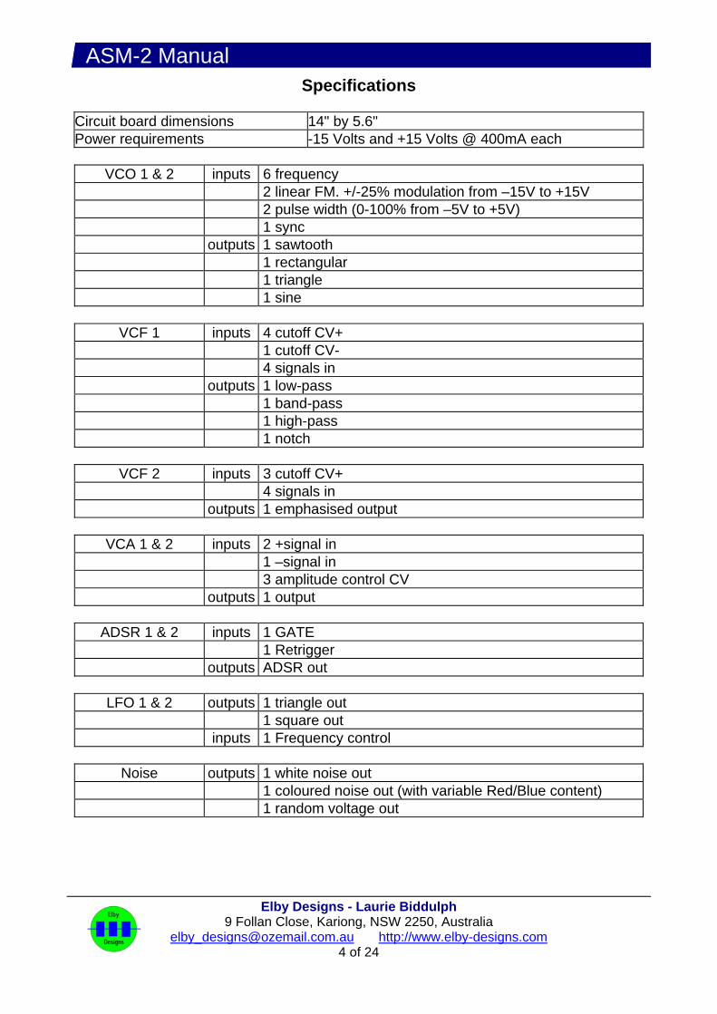
Specifications
Circuit board dimensions 14" by 5.6" Power requirements -15 Volts and +15 Volts @ 400mA each
VCO 1 & 2 inputs 6 frequency
2 linear FM. +/-25% modulation from –15V to +15V 2 pulse width (0-100% from –5V to +5V) 1 sync outputs 1 sawtooth 1 rectangular 1 triangle 1 sine
VCF 1 inputs 4 cutoff CV+
1 cutoff CV- 4 signals in outputs 1 low-pass 1 band-pass 1 high-pass 1 notch
VCF 2 inputs 3 cutoff CV+
4 signals in outputs 1 emphasised output
VCA 1 & 2 inputs 2 +signal in
1 –signal in 3 amplitude control CV outputs 1 output
ADSR 1 & 2 inputs 1 GATE
1 Retrigger outputs ADSR out
LFO 1 & 2 outputs 1 triangle out
1 square out inputs 1 Frequency control
Noise outputs 1 white noise out
1 coloured noise out (with variable Red/Blue content) 1 random voltage out
ASM-2 Manual
Elby Designs - Laurie Biddulph 9 Follan Close, Kariong, NSW 2250, Australia
[email protected] http://www.elby-designs.com 5 of 24
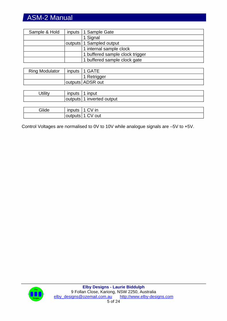
Sample & Hold inputs 1 Sample Gate
1 Signal outputs 1 Sampled output 1 internal sample clock 1 buffered sample clock trigger 1 buffered sample clock gate
Ring Modulator inputs 1 GATE
1 Retrigger outputs ADSR out
Utility inputs 1 input
outputs 1 inverted output
Glide inputs 1 CV in outputs 1 CV out
Control Voltages are normalised to 0V to 10V while analogue signals are –5V to +5V.
ASM-2 Manual
Elby Designs - Laurie Biddulph 9 Follan Close, Kariong, NSW 2250, Australia
[email protected] http://www.elby-designs.com 6 of 24
Circuit Descriptions
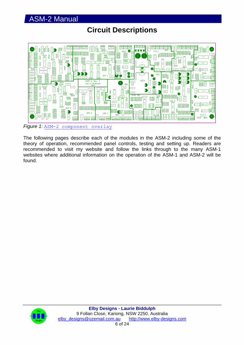
Figure 1: ASM-2 component overlay The following pages describe each of the modules in the ASM-2 including some of the theory of operation, recommended panel controls, testing and setting up. Readers are recommended to visit my website and follow the links through to the many ASM-1 websites where additional information on the operation of the ASM-1 and ASM-2 will be found.

ASM-2 Manual
Elby Designs - Laurie Biddulph 9 Follan Close, Kariong, NSW 2250, Australia
[email protected] http://www.elby-designs.com 7 of 24
VCO - Voltage Controlled Oscillator
Figure 2: Voltage controlled oscillator
The voltage controlled oscillators (VCOs) are the heart of any synthesiser. The quality of the VCOs ultimately determines the performance of the synthesiser. The two principal requirements of a synthesiser VCO are stability and good tracking. Stability means that if the control voltage applied to the VCO remains constant, then the frequency of the VCO should also remain constant and not drift. Tracking means that the VCO must follow the prescribed logarithmic 1 octave/Volt characteristic as closely as possible. In particular, where several VCOs are used they should all have similar characteristics. These parameters are particularly important in a chording instrument where a number of VCOs are used simultaneously. In a synthesiser using only one VCO slight drift or deviation from the 1 octave/Volt characteristic might not be noticed since the ear is not particularly good at judging absolute frequency, unless a person has `perfect pitch'. In any chording instrument however, even slight mis-tuning is immediately apparent due to the formation of beat notes. The VCO in the ASM-2 is an exponential sawtooth-based design substantially borrowed from Electronotes and has the following features:- • The frequency range of the VCO is from below 1Hz to above 100kHz. • The design has proved to be very stable and accurate.

ASM-2 Manual
Elby Designs - Laurie Biddulph 9 Follan Close, Kariong, NSW 2250, Australia
[email protected] http://www.elby-designs.com 8 of 24
Features: • CV (Logarithmic FM) Inputs (6) • Linear FM Inputs (2) • Sync Input • PWM Inputs (2) • Sawtooth Output, 10V p-p (centred around 0V) • Pulse Output, 10V p-p (centred around 0V) • Triangle Output, 10V p-p (centred around 0V) • Sine Output, 10V p-p (centred around 0V) How It Works: The VCO is an exponential sawtooth-based design substantially borrowed from an Electronotes design. It consists of a control voltage summing amplifier (U100A), driving an op-amp/NPN-pair exponential current source (Q101A, Q101B), which feeds a buffered-capacitor integrator (U101 and C104) with a FET discharge (Q100), controlled by a fast comparator (U102). Control Voltage summing amplifier: The control voltage amplifier is built around a virtual ground current summer based on the op-amp U100A, the resistor R108 and the pot P107. The scaling is set such that a sensitivity of 1V per Octave is achieved when sent through a 100k Ohm resistor. The actual scale over the R129/R130/R137 resistor divider needs to be slightly more than 1V/Oct, due to divider chain imperfections, and P107 is used to trim the actual gain of the summer. This is sensed as a scale trimming. The offset trimmer P100 is used to set the (externally) unmodulated tone. Waveshapers: The five-volt unipolar sawtooth is inverted (U103A, R109 and R140) and level shifted (R136/P103) to produce a ten-volt bipolar sawtooth for output. Another comparator (U100D) is used to produce a variable-width rectangular waveform from the sawtooth, with its own pulse-width control voltage summing amplifier (U100B). The ASM-2 VCO’s includes two more waveshaping circuits that generate a triangle and simple-sinewave.
ASM-2 Manual
Elby Designs - Laurie Biddulph 9 Follan Close, Kariong, NSW 2250, Australia
[email protected] http://www.elby-designs.com 9 of 24
VCF - Voltage Controlled Filter (VCF 1)
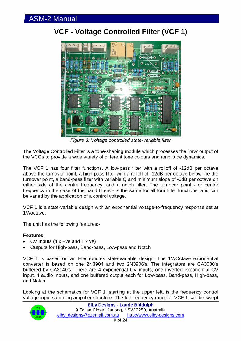
Figure 3: Voltage controlled state-variable filter The Voltage Controlled Filter is a tone-shaping module which processes the `raw' output of the VCOs to provide a wide variety of different tone colours and amplitude dynamics. The VCF 1 has four filter functions. A low-pass filter with a rolloff of -12dB per octave above the turnover point, a high-pass filter with a rolloff of -12dB per octave below the the turnover point, a band-pass filter with variable Q and minimum slope of -6dB per octave on either side of the centre frequency, and a notch filter. The turnover point - or centre frequency in the case of the band filters - is the same for all four filter functions, and can be varied by the application of a control voltage. VCF 1 is a state-variable design with an exponential voltage-to-frequency response set at 1V/octave. The unit has the following features:- Features: • CV Inputs (4 x +ve and 1 x ve) • Outputs for High-pass, Band-pass, Low-pass and Notch VCF 1 is based on an Electronotes state-variable design. The 1V/Octave exponential converter is based on one 2N3904 and two 2N3906's. The integrators are CA3080's buffered by CA3140's. There are 4 exponential CV inputs, one inverted exponential CV input, 4 audio inputs, and one buffered output each for Low-pass, Band-pass, High-pass, and Notch. Looking at the schematics for VCF 1, starting at the upper left, is the frequency control voltage input summing amplifier structure. The full frequency range of VCF 1 can be swept

ASM-2 Manual
Elby Designs - Laurie Biddulph 9 Follan Close, Kariong, NSW 2250, Australia
[email protected] http://www.elby-designs.com 10 of 24
with a control voltage from -15V to +15V (higher voltage means higher frequencies) applied to any of the CV input resistors. You can use higher resistances for inputs with less sweep range. An inverting amplifier is provided to allow positive modulation voltages to drop the VCF frequency. A 47K resistor is shown on the input to this inverter, which means that this input will have twice the "normal" sensitivity, or 0.5 volts per octave. You can put the traditional 100k value here, or any other value. The intention here is to use a panel pot as an attenuator for modulation depth control, both on the inverting modulation input as well as on one of the positive inputs. The signal input resistor can be 100K for unity gain of the VCF. However, if you run the VCO inputs straight in, the filter will distort a little, sounding like an MS-20 with the VCO's at full volume. I'd recommend putting input level controls on all four inputs - you'll be glad you did.
ASM-2 Manual
Elby Designs - Laurie Biddulph 9 Follan Close, Kariong, NSW 2250, Australia
[email protected] http://www.elby-designs.com 11 of 24
VCF - Voltage Controlled Filter (VCF 2)
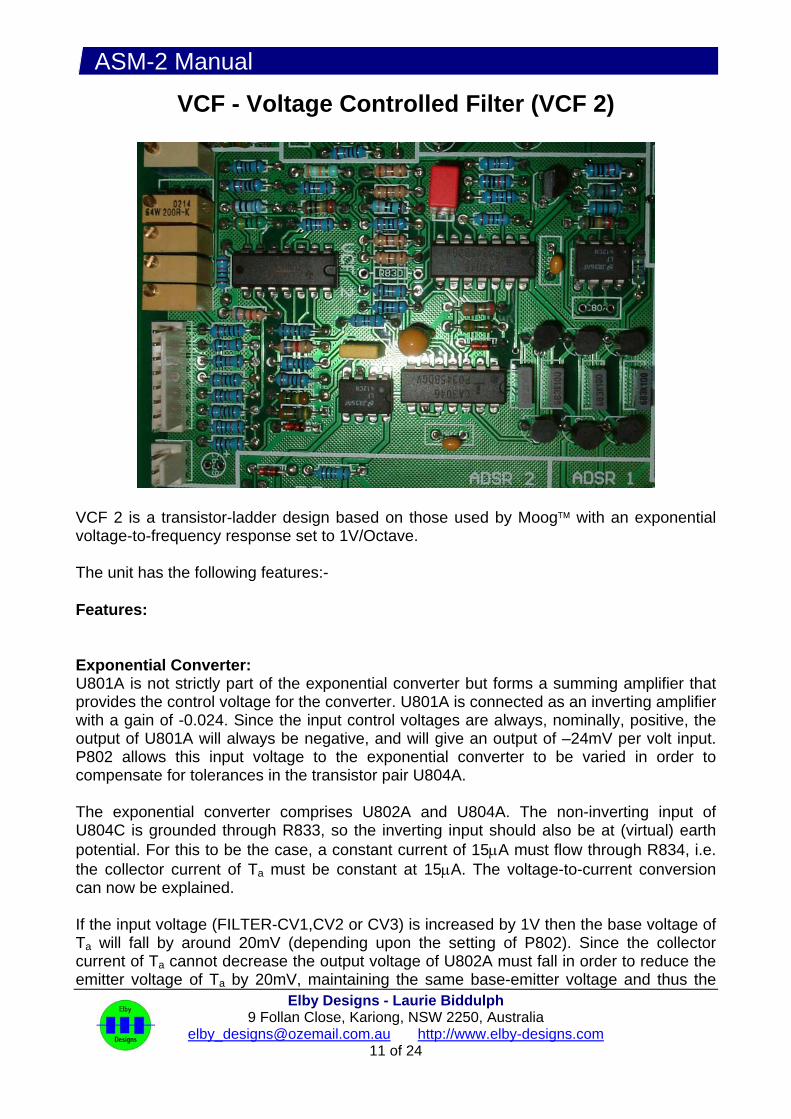
VCF 2 is a transistor-ladder design based on those used by Moog™ with an exponential voltage-to-frequency response set to 1V/Octave. The unit has the following features:- Features: Exponential Converter: U801A is not strictly part of the exponential converter but forms a summing amplifier that provides the control voltage for the converter. U801A is connected as an inverting amplifier with a gain of -0.024. Since the input control voltages are always, nominally, positive, the output of U801A will always be negative, and will give an output of –24mV per volt input. P802 allows this input voltage to the exponential converter to be varied in order to compensate for tolerances in the transistor pair U804A. The exponential converter comprises U802A and U804A. The non-inverting input of U804C is grounded through R833, so the inverting input should also be at (virtual) earth potential. For this to be the case, a constant current of 15μA must flow through R834, i.e. the collector current of Ta must be constant at 15μA. The voltage-to-current conversion can now be explained. If the input voltage (FILTER-CV1,CV2 or CV3) is increased by 1V then the base voltage of Ta will fall by around 20mV (depending upon the setting of P802). Since the collector current of Ta cannot decrease the output voltage of U802A must fall in order to reduce the emitter voltage of Ta by 20mV, maintaining the same base-emitter voltage and thus the
ASM-2 Manual
Elby Designs - Laurie Biddulph 9 Follan Close, Kariong, NSW 2250, Australia
[email protected] http://www.elby-designs.com 12 of 24
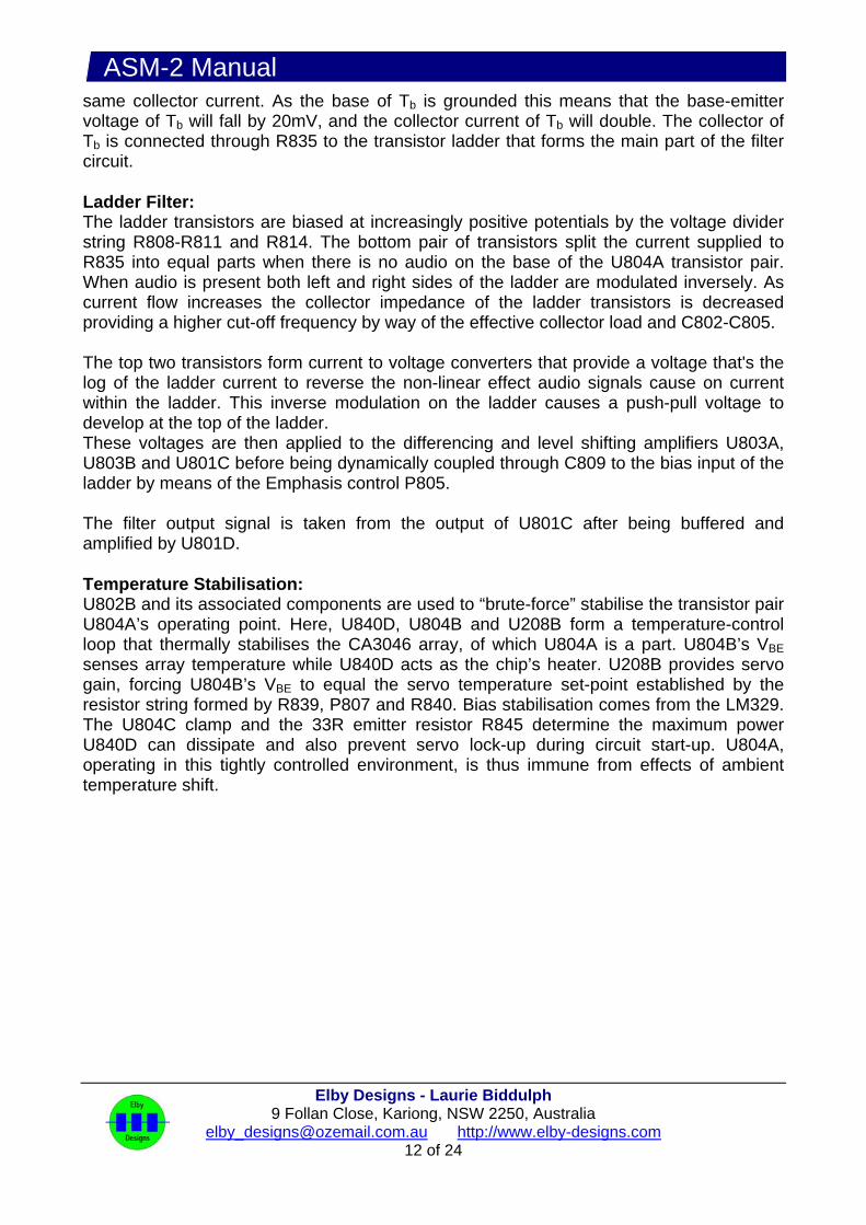
same collector current. As the base of Tb is grounded this means that the base-emitter voltage of Tb will fall by 20mV, and the collector current of Tb will double. The collector of Tb is connected through R835 to the transistor ladder that forms the main part of the filter circuit. Ladder Filter: The ladder transistors are biased at increasingly positive potentials by the voltage divider string R808-R811 and R814. The bottom pair of transistors split the current supplied to R835 into equal parts when there is no audio on the base of the U804A transistor pair. When audio is present both left and right sides of the ladder are modulated inversely. As current flow increases the collector impedance of the ladder transistors is decreased providing a higher cut-off frequency by way of the effective collector load and C802-C805. The top two transistors form current to voltage converters that provide a voltage that's the log of the ladder current to reverse the non-linear effect audio signals cause on current within the ladder. This inverse modulation on the ladder causes a push-pull voltage to develop at the top of the ladder. These voltages are then applied to the differencing and level shifting amplifiers U803A, U803B and U801C before being dynamically coupled through C809 to the bias input of the ladder by means of the Emphasis control P805. The filter output signal is taken from the output of U801C after being buffered and amplified by U801D. Temperature Stabilisation: U802B and its associated components are used to “brute-force” stabilise the transistor pair U804A’s operating point. Here, U840D, U804B and U208B form a temperature-control loop that thermally stabilises the CA3046 array, of which U804A is a part. U804B’s VBE senses array temperature while U840D acts as the chip’s heater. U208B provides servo gain, forcing U804B’s VBE to equal the servo temperature set-point established by the resistor string formed by R839, P807 and R840. Bias stabilisation comes from the LM329. The U804C clamp and the 33R emitter resistor R845 determine the maximum power U840D can dissipate and also prevent servo lock-up during circuit start-up. U804A, operating in this tightly controlled environment, is thus immune from effects of ambient temperature shift.

ASM-2 Manual
Elby Designs - Laurie Biddulph 9 Follan Close, Kariong, NSW 2250, Australia
[email protected] http://www.elby-designs.com 13 of 24
ADSR (1) (2) Envelope Generator
This ADSR (Attack, Decay, Sustain and Release) circuit was designed by Gene Stopp using a CMOS flip-flop and analog switches to charge and discharge the timing capacitor. The ADSR (Attack-Decay-Sustain-Release) module is used to control the VCF and VCA modules and thereby determine the dynamic harmonic structure and dynamic amplitude characteristic of the VCO signals.
Figure 4: Envelope Generator It is often not realised, even by musicians, how much the character of an instrument is determined by the dynamic amplitude and harmonic behaviour, rather than by the steady-state harmonic content of an instrument. If the attack and decay periods of a note are artificially modified, then the whole character of the sound is altered. For example, starting with a triangle output from the VCO, a whole range of instrument sounds can be produced simply by varying the amplitude envelope, ranging from `soft' sounds such as flute and some organ voices, to `hard' percussive sounds such as piano and xylophone. Envelope control of the harmonic content using the VCF allows even greater variation in the character of the sound. The ADSR module will generate Attack-Decay-Sustain-Release control signals upon receipt of a positive GATE signal. Irrespective of the length of the GATE signal the ADSR will always generate an Attack-Release curve. Decay and Sustain portions of the curve are dependent upon the presence of the GATE signal for a minimum time as follows:- If GateOn = Attack + Decay, then ADR = GateOn + Release. For example, if Attack is set to 2mS and Decay is set to 3mS then, if the Gate is on for more than 2mS (Attack time) and is equal to or less than 5mS (Attack + Decay) then you will get an ADR curve. If GateOn = Attack + Decay + Sustain, then ADSR = GateOn + Release. The Sustain time will be equal to the difference between the GateOn time and the total of Attack + Decay. For example, if Attack is set to 2mS and Decay is set to 3mS then, if the Gate is on for, say, 8mS then you will get an ADSR curve where the Sustain period will be 3mS (8mS – 5mS).

ASM-2 Manual
Elby Designs - Laurie Biddulph 9 Follan Close, Kariong, NSW 2250, Australia
[email protected] http://www.elby-designs.com 14 of 24
The ADSR module has the following features:- Specification: • Attack time - 1ms to 5s • Decay time - 1ms to 10s • Release time - 1ms to 10s • Sustain level - 0V to +10V Features: • Gate In • Retrigger In • Envelope Out (maximum is adjustable from 0V to +12V) How It Works: A positive going GATE signal arrives at U402 and provides both a positive and a negative logic drive signal (pins 1 and 7 respectively). The positive output (U402-pin 1) sets U403C to the DECAY/SUSTAIN position and, via a pulse generated through C402/R402, sets the flip-flop U404 causing U403B to switch to the ATTACK position (pin 15 and pin 1 closed). In this position the envelope capacitor C401 is charged via the ATTACK pot P405. Opamp U401B is a voltage follower and the exponential charge curve on C401 is presented to the ENVELOPE OUT (U401B pin 7). A portion of this signal is fed through the trimmer P406 to a `reset' pin on the flip-flop so that when the ATTACK curve reaches a predefined peak, it causes the flip-flop to reset. U403B then switches to the DECAY/SUSTAIN/RELEASE position (pin 15 and pin 2 closed) and, with U403B now in the DECAY/SUSTAIN position (pin 14 and pin 13 closed), the envelope capacitor starts to discharge through P403 and the opamp U401A. The envelope capacitor will, however, only discharge until the voltage on the capacitor equals the SUSTAIN level at the output of U401A (as set by the SUSTAIN pot P402). If the GATE is still on at this stage, the envelope capacitor will remain charged to the SUSTAIN level until the GATE is released at which point U403B returns to the RELEASE position (pin 14 and pin 12 closed) and connects the RELEASE pot P404 to the envelope capacitor. The envelope capacitor now discharges fully providing the RELEASE curve of the envelope. The above description assumes that the GATE-on time is greater than the total of the ATTACK and DECAY times added together, in which case a full ADSR envelope is achieved with the SUSTAIN-on time being equal to the sum of the GATE time minus the ATTACK + DECAY times i.e SUSTAIN(on) = GATE(on) - ATTACK(on) - DECAY(on) Releasing the GATE signal earlier will result in only a portion of the Attack-Decay-Sustain curves being completed. The RELEASE curve is ALWAYS initiated as soon as the GATE is released. Depending upon the GATE-on time the resultant envelope will be either AR, ADR or ADSR.
ASM-2 Manual
Elby Designs - Laurie Biddulph 9 Follan Close, Kariong, NSW 2250, Australia
[email protected] http://www.elby-designs.com 15 of 24
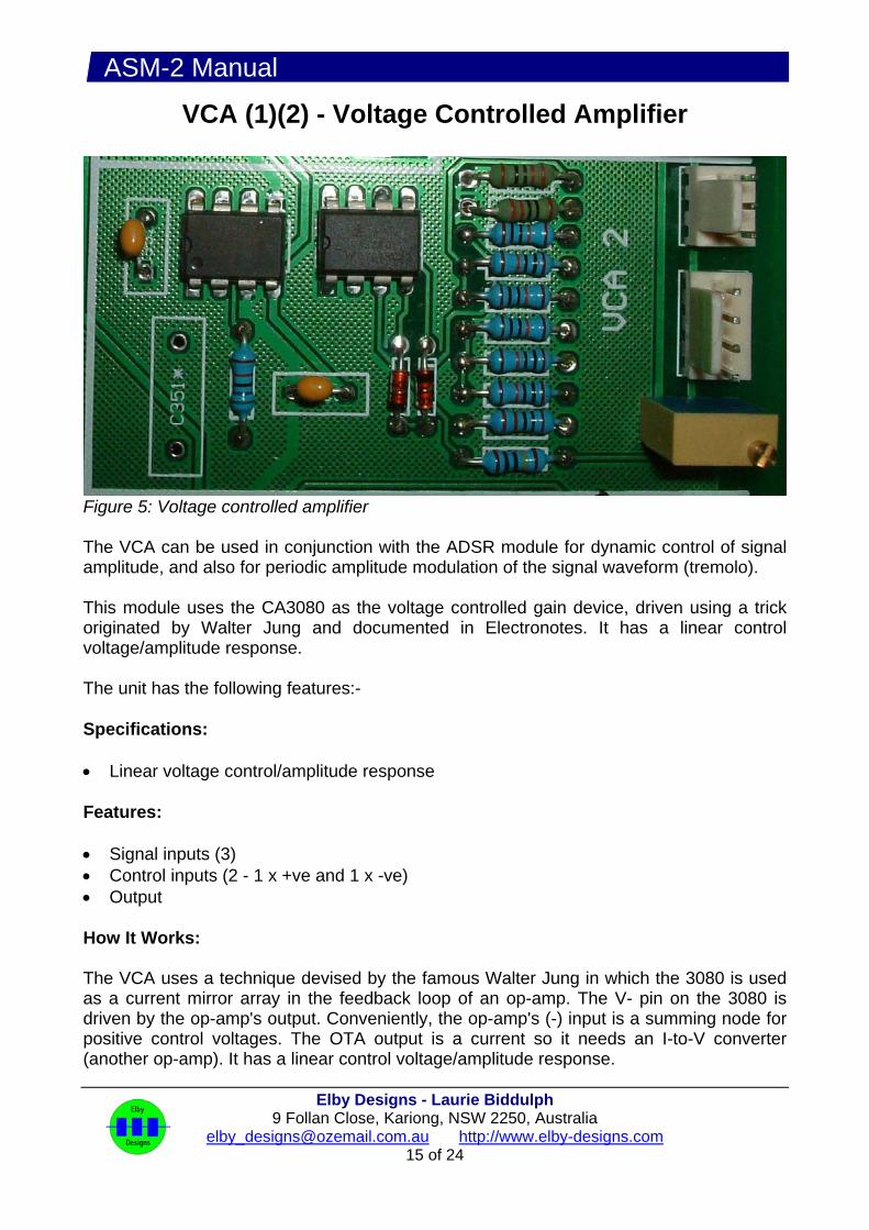
VCA (1)(2) - Voltage Controlled Amplifier
Figure 5: Voltage controlled amplifier The VCA can be used in conjunction with the ADSR module for dynamic control of signal amplitude, and also for periodic amplitude modulation of the signal waveform (tremolo). This module uses the CA3080 as the voltage controlled gain device, driven using a trick originated by Walter Jung and documented in Electronotes. It has a linear control voltage/amplitude response. The unit has the following features:- Specifications: • Linear voltage control/amplitude response Features: • Signal inputs (3) • Control inputs (2 - 1 x +ve and 1 x -ve) • Output How It Works: The VCA uses a technique devised by the famous Walter Jung in which the 3080 is used as a current mirror array in the feedback loop of an op-amp. The V- pin on the 3080 is driven by the op-amp's output. Conveniently, the op-amp's (-) input is a summing node for positive control voltages. The OTA output is a current so it needs an I-to-V converter (another op-amp). It has a linear control voltage/amplitude response.
ASM-2 Manual
Elby Designs - Laurie Biddulph 9 Follan Close, Kariong, NSW 2250, Australia
[email protected] http://www.elby-designs.com 16 of 24
Power up, Testing and Calibration Procedures: The OFFSET trimpot is adjusted for zero volts at the VCA output with one of the control inputs at +5 volts and the other two unconnected. About the VCA inputs: The (-) input on the VCA is just an extra input that happens to invert the signal as it goes through the VCA. The VCA's on most synthesisers have this capability but it's just not always brought out to a panel jack. The Moog 902 for example has two input jacks, and the upper one is (+) and the lower one is (-), and it's not even labelled on the panel! In practice for audio signals there is not much difference between the two (as long as you watch out for cancellation effects with signals that originate from the same sources within a modular system). For low frequency modulation applications, the (-) input can be used to invert the signal whose amplitude is being controlled by the VCA - therefore you can use the VCA as a voltage-controlled inverter. Problems: • There may be some high-frequency oscillation on the VCA output – if there is, add a
10pf cap across output amp gain resistor R309/R359. A space has been provided on the pcb for this component (C301 & C351).
Enhancements: It is recommended that CV3 of the VCA be connected to a 100K Linear Pot to provide an `Initial Gain’ setting. By adding a 91K resistor between CCW pad of this pot and -15V, the initial gain can be taken a little negative when you turn it down all the way. This will ensure that the VCA shuts off completely. This way you can make the turn-on voltage from another module a little higher than zero volts.

ASM-2 Manual
Elby Designs - Laurie Biddulph 9 Follan Close, Kariong, NSW 2250, Australia
[email protected] http://www.elby-designs.com 17 of 24
Noise Module
Figure 6: Noise module The Noise module provides the basic material to produce a whole spectrum of sounds that do not have a defined pitch. White noise can be used to produce sounds such as wind, rain and surf. `Coloured' noise, which is white noise with the low frequency components boosted, is used for sounds having a strong bass content, such as the rumbling of thunder. In addition to modulating the VCO signals, noise can be added to these signals to simulate wind noise in organ pipes and woodwind instruments. Connectors: • White Noise (~5V peak-to-peak) • Coloured Noise (~5V peak-to-peak) • Random Voltage (~5V peak-to-peak) How It Works: This circuit uses a reverse-biased NPN transistor as the noise source. This provides good clean wide-band white noise in its purest analog form - the only problem is that it's a really tiny signal and needs lots of amplification. The subsequent op-amp stages boost the noise level and also provide the filtering for White, Pink and Random Noise outputs.
ASM-2 Manual
Elby Designs - Laurie Biddulph 9 Follan Close, Kariong, NSW 2250, Australia
[email protected] http://www.elby-designs.com 18 of 24
The white noise is also fed into a filter constructed around U602, which has two stages:- • U602B produces a filtered `coloured' noise source in which the bass end is boosted,
and • U602A the `Coloured' noise signal is further filtered by a low-pass filter which passes
only very low frequency components to produce an extremely low frequency 'random voltage'.
The +/-15V supplies for these op-amps are filtered by a pair of RC networks (composed of the 22ohm/10uF components). The Noise module in the ASM-2 differs from the ASM-1 version by the inclusion of a dual adjustable filter stage in the `coloured noise section’ offering adjustment over the `blue’ and the `red’ content of the coloured noise. If you do not wish to have this Red/Blue filter and would like to retain the original ASM-1 Noise arrangement then you will need to make the following small adjustments to the component values:- 1. Remove P602, P603, C604, C605 and R611, 2. Replace R609, R610 and C606 with wire links, 3. Fit link LK601, 4. Fit R607 with 100K, 5. Replace C603 with 10nF, 6. Replace C607 with 1nF, 7. Replace R608 with 47K, and 8. Fit a 270K resistor across the 2 end terminations in location P603 Readers should refer to the schematic “ASM-2 Noise to ASM-1 Noise.pdf” which can be found the “The Original ASM-1” folder on the support CD.

ASM-2 Manual
Elby Designs - Laurie Biddulph 9 Follan Close, Kariong, NSW 2250, Australia
[email protected] http://www.elby-designs.com 19 of 24
VCLFO (1)(2) - Low Frequency Oscillator
Figure 7: Voltage controlled low-frequency oscillator Mention has already been made of the fact that conventional instruments exhibit more `life' and variation in tonal character than electronic instruments due to the way in which they are played. For example, string instruments and woodwind instruments can exhibit marked tremolo and/or vibrato due to variations in the bowing or blowing. The keyboard of a synthesiser provides a relatively inflexible and expressionless means of playing that does not allow these nuances to be introduced into the sound, and in order to make the sound more `lively' amplitude and frequency modulation must be introduced using LFOs and noise sources. The VCLFO module described here provides two low-frequency waveforms. Specifications: • Frequency (Square & Triangle) - 0.1Hz < frequency > 120Hz • Square and Triangle outputs - 10V peak-to-peak centred around 0V How It Works: The basic oscillator circuit consists of the two op-amps U502A and U501C connected respectively as an integrator and a Schmitt trigger. When the output of U501C is positive the positive voltage output of U501C is applied to P503, so a current (dependent on the wiper position of P503) flows in to the integrator through R508. The output of U502A ramps negative until it reaches about –5V, when the voltage on the non-inverting input of U501C will fall below the voltage on the inverting input (zero volts) and the output of

ASM-2 Manual
Elby Designs - Laurie Biddulph 9 Follan Close, Kariong, NSW 2250, Australia
[email protected] http://www.elby-designs.com 20 of 24
U501C will swing negative. The negative output voltage of U501C is applied to P503. Current will flow out of the integrator through R508, and the integrator output will ramp positive until it reaches about +5V, when the voltage on the non-inverting input of U501C will rise above zero and the output of U501C will swing positive. The whole cycle then repeats. The output from U502A is thus a triangular waveform with a peak-to-peak voltage of about 10V, while at the output of U501C a square-wave of the same frequency is available. P503 is used to adjust the frequency of the VCLFO by varying the voltage applied to the integrator input, which alters the integrator input current and hence the rate at which the integrator ramps positive or negative. The value of R507 determines the minimum integrator input voltage that can be set by P503, and hence the minimum frequency of the VCLFO. The value of R507 must not be chosen too high or the minimum frequency of the VCLFO will be too great. On the other hand it should not be chosen too low, or the minimum integrator input current at the minimum setting of P503 will be comparable with the input currents of U502A. This will result in unreliable operation of the oscillator at low frequencies. The optimum value for R507 is 47 ohms, but the user is free to experiment with this for best results. The squarewave at the output of U501C has an amplitude of +/-15 volts, so the resistor attenuator network R512/R515 has been included in the output path to provide the standard +/-5 volt level. Voltage control of the VCLFO is introduced by applying a control voltage to a half-wave rectifier circuit built around U501A and U501B and then taking the resultant output and injecting it as an offset voltage to the integrator input voltage. An LED Indicator circuit is built around U501D and provides a visual indication of the operational state of the VCLFO. The triangle output is fed to this circuit resulting in the LED intensity following the amplitude of the VCLFO output.

ASM-2 Manual
Elby Designs - Laurie Biddulph 9 Follan Close, Kariong, NSW 2250, Australia
[email protected] http://www.elby-designs.com 21 of 24
Glide Buffer
When playing up and down a scale the control voltage from a keyboard would consist of a series of discrete steps. This would give rise to equally discrete changes of pitch, the minimum change in pitch being one semitone interval on the tempered scale, as with any other keyboard instrument. However, many instruments are characterised by the ability to make continuous (smooth) changes of pitch, one example being the trombone with its slide. This style of playing is known as `portamento'.
Figure 8: Glide module The addition of this circuit between the keyboard control voltage and the VCO’s allows the user to vary the degree of glide or portamento applied. How It Works: The first buffer, built around U701A, provides a low-impedance source for the glide pot which in turn with C701 provides an RC time delay on the control voltage. The resultant voltage on the C701 is then buffered by U701B, which also provides a low-impedance source for the following modules. Power up, Testing and Calibration Procedures The Glide module does not require any setting. As long as a good quality, low-leakage component is used for the capacitor then you should get consistent results. Enhancements: The Glide circuit on the ASM-2 provides for both an exponential control and a linear control curve. Selection of the control curve is made via a set of jumpers on the pcb which can, alternatively, be wired to a DPDT switch on your front panel.

ASM-2 Manual
Elby Designs - Laurie Biddulph 9 Follan Close, Kariong, NSW 2250, Australia
[email protected] http://www.elby-designs.com 22 of 24
Ring Modulator
Figure 9: Ring Modulator A ring modulator is a simple device that can be used to create unusual sounds from an instruments output. It effectively takes two signals (each with some frequency component), and produces a signal containing the sum and differences of those frequencies. These frequencies will typically be non-harmonic, so the ring modulator can create some very dissonant sounds.
A very simple example of this affect is shown above where the two input signals (a) at 400Hz and (b) 600Hz produce the output (c) which consists of the difference frequency (200Hz) and the sum frequency (1000Hz). The output waveform can become very complex if the input waveforms themselves contain harmonics.
ASM-2 Manual
Elby Designs - Laurie Biddulph 9 Follan Close, Kariong, NSW 2250, Australia
[email protected] http://www.elby-designs.com 23 of 24
The heart of the ASM-2 Ring-Modulator is U1601, a double-balanced modulator, which is responsible for multiplying the input signals. The IC used is the LM1496N from National (or the MC1496P from Motorola). A number of external resistors are required for the IC to function satisfactorily. It is necessary to limit the amplitude of the two input signals, otherwise there is the danger that the input signals will not be sufficiently suppressed and will appear at the output. For this reason the input signals are held to a reasonable level (maximum approximately 150mVpp) with the aid of the divider networks R1601/R1603 and R1608/R1611. This has the effect of ensuring that the inputs signals are approximately 50dB down at the output. The suppression can be optimised by means of adjusting potentiometers P1601 and P1602. R1606 and R1607 set the correct DC offset voltages at pin 8 and 10 of the IC, whilst the remaining associated resistors round the IC ensure the correct DC bias currents. The output voltage of the IC is tailored to give an output level of 1.5Vpp which is then amplified and buffered, by U1602A, to match the standard ASM-2 level of 10Vpp.
ASM-2 Manual
Elby Designs - Laurie Biddulph 9 Follan Close, Kariong, NSW 2250, Australia
[email protected] http://www.elby-designs.com 24 of 24
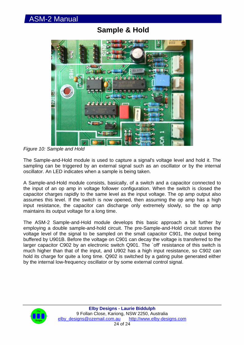
Sample & Hold
Figure 10: Sample and Hold The Sample-and-Hold module is used to capture a signal's voltage level and hold it. The sampling can be triggered by an external signal such as an oscillator or by the internal oscillator. An LED indicates when a sample is being taken. A Sample-and-Hold module consists, basically, of a switch and a capacitor connected to the input of an op amp in voltage follower configuration. When the switch is closed the capacitor charges rapidly to the same level as the input voltage. The op amp output also assumes this level. If the switch is now opened, then assuming the op amp has a high input resistance, the capacitor can discharge only extremely slowly, so the op amp maintains its output voltage for a long time. The ASM-2 Sample-and-Hold module develops this basic approach a bit further by employing a double sample-and-hold circuit. The pre-Sample-and-Hold circuit stores the voltage level of the signal to be sampled on the small capacitor C901, the output being buffered by U901B. Before the voltage on C901 can decay the voltage is transferred to the larger capacitor C902 by an electronic switch Q901. The `off’ resistance of this switch is much higher than that of the input, and U902 has a high input resistance, so C902 can hold its charge for quite a long time. Q902 is switched by a gating pulse generated either by the internal low-frequency oscillator or by some external control signal.